EP2212249B1 - Process for the production of medium and high purity silicon from metallurgical grade silicon - Google Patents
Process for the production of medium and high purity silicon from metallurgical grade silicon Download PDFInfo
- Publication number
- EP2212249B1 EP2212249B1 EP08733596.4A EP08733596A EP2212249B1 EP 2212249 B1 EP2212249 B1 EP 2212249B1 EP 08733596 A EP08733596 A EP 08733596A EP 2212249 B1 EP2212249 B1 EP 2212249B1
- Authority
- EP
- European Patent Office
- Prior art keywords
- silicon
- process according
- ingot
- mould
- melt
- Prior art date
- Legal status (The legal status is an assumption and is not a legal conclusion. Google has not performed a legal analysis and makes no representation as to the accuracy of the status listed.)
- Active
Links
- 229910052710 silicon Inorganic materials 0.000 title claims description 112
- 239000010703 silicon Substances 0.000 title claims description 111
- 238000000034 method Methods 0.000 title claims description 51
- 230000008569 process Effects 0.000 title claims description 41
- 238000004519 manufacturing process Methods 0.000 title description 11
- 238000007711 solidification Methods 0.000 claims description 83
- 230000008023 solidification Effects 0.000 claims description 83
- 239000007788 liquid Substances 0.000 claims description 78
- 239000007787 solid Substances 0.000 claims description 53
- 239000000155 melt Substances 0.000 claims description 43
- 239000012535 impurity Substances 0.000 claims description 30
- 229910052742 iron Inorganic materials 0.000 claims description 24
- 229910021420 polycrystalline silicon Inorganic materials 0.000 claims description 21
- 229910052698 phosphorus Inorganic materials 0.000 claims description 20
- OAICVXFJPJFONN-UHFFFAOYSA-N Phosphorus Chemical compound [P] OAICVXFJPJFONN-UHFFFAOYSA-N 0.000 claims description 17
- 229910052796 boron Inorganic materials 0.000 claims description 17
- 239000011574 phosphorus Substances 0.000 claims description 17
- 238000003756 stirring Methods 0.000 claims description 17
- ZOXJGFHDIHLPTG-UHFFFAOYSA-N Boron Chemical compound [B] ZOXJGFHDIHLPTG-UHFFFAOYSA-N 0.000 claims description 14
- 229910052799 carbon Inorganic materials 0.000 claims description 13
- 229910052751 metal Inorganic materials 0.000 claims description 13
- 239000002184 metal Substances 0.000 claims description 13
- OKTJSMMVPCPJKN-UHFFFAOYSA-N Carbon Chemical compound [C] OKTJSMMVPCPJKN-UHFFFAOYSA-N 0.000 claims description 11
- 229910052760 oxygen Inorganic materials 0.000 claims description 11
- 239000001301 oxygen Substances 0.000 claims description 10
- QVGXLLKOCUKJST-UHFFFAOYSA-N atomic oxygen Chemical compound [O] QVGXLLKOCUKJST-UHFFFAOYSA-N 0.000 claims description 9
- 238000009413 insulation Methods 0.000 claims description 9
- 229910052782 aluminium Inorganic materials 0.000 claims description 8
- 230000015572 biosynthetic process Effects 0.000 claims description 7
- 229910052791 calcium Inorganic materials 0.000 claims description 7
- 238000000605 extraction Methods 0.000 claims description 7
- 229910052787 antimony Inorganic materials 0.000 claims description 6
- 229910052785 arsenic Inorganic materials 0.000 claims description 6
- 229910052793 cadmium Inorganic materials 0.000 claims description 6
- 229910052804 chromium Inorganic materials 0.000 claims description 6
- 239000000356 contaminant Substances 0.000 claims description 6
- 229910052802 copper Inorganic materials 0.000 claims description 6
- 210000001787 dendrite Anatomy 0.000 claims description 6
- 229910052746 lanthanum Inorganic materials 0.000 claims description 6
- 229910052745 lead Inorganic materials 0.000 claims description 6
- 229910052749 magnesium Inorganic materials 0.000 claims description 6
- 229910052748 manganese Inorganic materials 0.000 claims description 6
- 229910052759 nickel Inorganic materials 0.000 claims description 6
- 229910052712 strontium Inorganic materials 0.000 claims description 6
- 229910052719 titanium Inorganic materials 0.000 claims description 6
- 229910052720 vanadium Inorganic materials 0.000 claims description 6
- 229910052725 zinc Inorganic materials 0.000 claims description 6
- 229910052726 zirconium Inorganic materials 0.000 claims description 6
- XLYOFNOQVPJJNP-UHFFFAOYSA-N water Substances O XLYOFNOQVPJJNP-UHFFFAOYSA-N 0.000 claims description 5
- 239000002826 coolant Substances 0.000 claims description 4
- 229910052700 potassium Inorganic materials 0.000 claims description 4
- 230000008018 melting Effects 0.000 claims description 2
- 238000002844 melting Methods 0.000 claims description 2
- XUIMIQQOPSSXEZ-UHFFFAOYSA-N Silicon Chemical compound [Si] XUIMIQQOPSSXEZ-UHFFFAOYSA-N 0.000 description 104
- XEEYBQQBJWHFJM-UHFFFAOYSA-N Iron Chemical compound [Fe] XEEYBQQBJWHFJM-UHFFFAOYSA-N 0.000 description 49
- 238000000746 purification Methods 0.000 description 10
- 238000013019 agitation Methods 0.000 description 9
- 239000011575 calcium Substances 0.000 description 9
- 238000002474 experimental method Methods 0.000 description 8
- VYPSYNLAJGMNEJ-UHFFFAOYSA-N Silicium dioxide Chemical compound O=[Si]=O VYPSYNLAJGMNEJ-UHFFFAOYSA-N 0.000 description 7
- 239000010410 layer Substances 0.000 description 7
- 210000004027 cell Anatomy 0.000 description 6
- 238000009826 distribution Methods 0.000 description 6
- 239000000523 sample Substances 0.000 description 6
- 238000005204 segregation Methods 0.000 description 6
- 238000004458 analytical method Methods 0.000 description 5
- 238000002425 crystallisation Methods 0.000 description 5
- 239000000203 mixture Substances 0.000 description 5
- 230000009467 reduction Effects 0.000 description 5
- 239000004065 semiconductor Substances 0.000 description 5
- 229910021422 solar-grade silicon Inorganic materials 0.000 description 5
- 239000003570 air Substances 0.000 description 4
- 230000008025 crystallization Effects 0.000 description 4
- 238000009792 diffusion process Methods 0.000 description 4
- 239000012452 mother liquor Substances 0.000 description 4
- 238000005070 sampling Methods 0.000 description 3
- 239000007858 starting material Substances 0.000 description 3
- 239000000725 suspension Substances 0.000 description 3
- 230000009471 action Effects 0.000 description 2
- XAGFODPZIPBFFR-UHFFFAOYSA-N aluminium Chemical compound [Al] XAGFODPZIPBFFR-UHFFFAOYSA-N 0.000 description 2
- 239000003610 charcoal Substances 0.000 description 2
- 239000003795 chemical substances by application Substances 0.000 description 2
- 229910021419 crystalline silicon Inorganic materials 0.000 description 2
- 238000010586 diagram Methods 0.000 description 2
- 238000010891 electric arc Methods 0.000 description 2
- 238000010438 heat treatment Methods 0.000 description 2
- 229910001338 liquidmetal Inorganic materials 0.000 description 2
- 238000010791 quenching Methods 0.000 description 2
- 230000000171 quenching effect Effects 0.000 description 2
- 238000007670 refining Methods 0.000 description 2
- 239000000377 silicon dioxide Substances 0.000 description 2
- 239000000126 substance Substances 0.000 description 2
- 238000004781 supercooling Methods 0.000 description 2
- 238000011282 treatment Methods 0.000 description 2
- 229910000789 Aluminium-silicon alloy Inorganic materials 0.000 description 1
- OYPRJOBELJOOCE-UHFFFAOYSA-N Calcium Chemical compound [Ca] OYPRJOBELJOOCE-UHFFFAOYSA-N 0.000 description 1
- ZAMOUSCENKQFHK-UHFFFAOYSA-N Chlorine atom Chemical compound [Cl] ZAMOUSCENKQFHK-UHFFFAOYSA-N 0.000 description 1
- 229910000831 Steel Inorganic materials 0.000 description 1
- 229910045601 alloy Inorganic materials 0.000 description 1
- 239000000956 alloy Substances 0.000 description 1
- 239000004411 aluminium Substances 0.000 description 1
- 239000012080 ambient air Substances 0.000 description 1
- 230000005587 bubbling Effects 0.000 description 1
- 239000000460 chlorine Substances 0.000 description 1
- 229910052801 chlorine Inorganic materials 0.000 description 1
- 239000003245 coal Substances 0.000 description 1
- 230000002860 competitive effect Effects 0.000 description 1
- 238000011109 contamination Methods 0.000 description 1
- 238000001816 cooling Methods 0.000 description 1
- 238000005336 cracking Methods 0.000 description 1
- 239000013078 crystal Substances 0.000 description 1
- 230000006837 decompression Effects 0.000 description 1
- 230000001419 dependent effect Effects 0.000 description 1
- 238000011161 development Methods 0.000 description 1
- 230000000694 effects Effects 0.000 description 1
- 230000004907 flux Effects 0.000 description 1
- 230000008014 freezing Effects 0.000 description 1
- 238000007710 freezing Methods 0.000 description 1
- 239000007789 gas Substances 0.000 description 1
- BHEPBYXIRTUNPN-UHFFFAOYSA-N hydridophosphorus(.) (triplet) Chemical compound [PH] BHEPBYXIRTUNPN-UHFFFAOYSA-N 0.000 description 1
- 230000006698 induction Effects 0.000 description 1
- 239000000463 material Substances 0.000 description 1
- 238000010907 mechanical stirring Methods 0.000 description 1
- 230000007246 mechanism Effects 0.000 description 1
- 238000005272 metallurgy Methods 0.000 description 1
- 238000012986 modification Methods 0.000 description 1
- 230000004048 modification Effects 0.000 description 1
- 238000005192 partition Methods 0.000 description 1
- 239000002006 petroleum coke Substances 0.000 description 1
- 238000009832 plasma treatment Methods 0.000 description 1
- 229920001296 polysiloxane Polymers 0.000 description 1
- 230000000135 prohibitive effect Effects 0.000 description 1
- 239000010453 quartz Substances 0.000 description 1
- 238000011160 research Methods 0.000 description 1
- 238000010079 rubber tapping Methods 0.000 description 1
- 239000004576 sand Substances 0.000 description 1
- 238000000926 separation method Methods 0.000 description 1
- 150000003376 silicon Chemical class 0.000 description 1
- 239000002210 silicon-based material Substances 0.000 description 1
- 239000010959 steel Substances 0.000 description 1
- 239000002344 surface layer Substances 0.000 description 1
- 235000012431 wafers Nutrition 0.000 description 1
- 238000005406 washing Methods 0.000 description 1
Images


Classifications
-
- C—CHEMISTRY; METALLURGY
- C01—INORGANIC CHEMISTRY
- C01B—NON-METALLIC ELEMENTS; COMPOUNDS THEREOF; METALLOIDS OR COMPOUNDS THEREOF NOT COVERED BY SUBCLASS C01C
- C01B33/00—Silicon; Compounds thereof
- C01B33/02—Silicon
- C01B33/037—Purification
-
- C—CHEMISTRY; METALLURGY
- C30—CRYSTAL GROWTH
- C30B—SINGLE-CRYSTAL GROWTH; UNIDIRECTIONAL SOLIDIFICATION OF EUTECTIC MATERIAL OR UNIDIRECTIONAL DEMIXING OF EUTECTOID MATERIAL; REFINING BY ZONE-MELTING OF MATERIAL; PRODUCTION OF A HOMOGENEOUS POLYCRYSTALLINE MATERIAL WITH DEFINED STRUCTURE; SINGLE CRYSTALS OR HOMOGENEOUS POLYCRYSTALLINE MATERIAL WITH DEFINED STRUCTURE; AFTER-TREATMENT OF SINGLE CRYSTALS OR A HOMOGENEOUS POLYCRYSTALLINE MATERIAL WITH DEFINED STRUCTURE; APPARATUS THEREFOR
- C30B11/00—Single-crystal growth by normal freezing or freezing under temperature gradient, e.g. Bridgman-Stockbarger method
- C30B11/006—Controlling or regulating
-
- C—CHEMISTRY; METALLURGY
- C30—CRYSTAL GROWTH
- C30B—SINGLE-CRYSTAL GROWTH; UNIDIRECTIONAL SOLIDIFICATION OF EUTECTIC MATERIAL OR UNIDIRECTIONAL DEMIXING OF EUTECTOID MATERIAL; REFINING BY ZONE-MELTING OF MATERIAL; PRODUCTION OF A HOMOGENEOUS POLYCRYSTALLINE MATERIAL WITH DEFINED STRUCTURE; SINGLE CRYSTALS OR HOMOGENEOUS POLYCRYSTALLINE MATERIAL WITH DEFINED STRUCTURE; AFTER-TREATMENT OF SINGLE CRYSTALS OR A HOMOGENEOUS POLYCRYSTALLINE MATERIAL WITH DEFINED STRUCTURE; APPARATUS THEREFOR
- C30B28/00—Production of homogeneous polycrystalline material with defined structure
- C30B28/04—Production of homogeneous polycrystalline material with defined structure from liquids
- C30B28/06—Production of homogeneous polycrystalline material with defined structure from liquids by normal freezing or freezing under temperature gradient
-
- C—CHEMISTRY; METALLURGY
- C30—CRYSTAL GROWTH
- C30B—SINGLE-CRYSTAL GROWTH; UNIDIRECTIONAL SOLIDIFICATION OF EUTECTIC MATERIAL OR UNIDIRECTIONAL DEMIXING OF EUTECTOID MATERIAL; REFINING BY ZONE-MELTING OF MATERIAL; PRODUCTION OF A HOMOGENEOUS POLYCRYSTALLINE MATERIAL WITH DEFINED STRUCTURE; SINGLE CRYSTALS OR HOMOGENEOUS POLYCRYSTALLINE MATERIAL WITH DEFINED STRUCTURE; AFTER-TREATMENT OF SINGLE CRYSTALS OR A HOMOGENEOUS POLYCRYSTALLINE MATERIAL WITH DEFINED STRUCTURE; APPARATUS THEREFOR
- C30B29/00—Single crystals or homogeneous polycrystalline material with defined structure characterised by the material or by their shape
- C30B29/02—Elements
- C30B29/06—Silicon
Definitions
- This invention relates generally to the production of silicon metal, more particularly it concerns a process of purification by crystallization that produces medium and/or high purity silicon metal for use in photovoltaic applications.
- Si silicon
- Metallurgical grade silicon is a silicon of low purity. Typically, metallurgical grade silicon that is about 98% pure silicon is produced via the reaction between carbon (coal, charcoal, pet coke) and silica (SiO 2 ) at a temperature around 1700 °C in a process known as carbothermal reduction.
- Metallurgical grade Si is diverted to the semiconductor industry for use in the production of Si wafers, etc.
- the semiconductor industry requires silicon of ultra-high purity, e.g. electronic grade silicon (EG-Si) having approximately a 99.9999999% purity (9N).
- EG-Si electronic grade silicon
- Metallurgical grade silicon must be purified to produce this electronic grade.
- the purification process is elaborate resulting in the higher cost of electronic grade silicon.
- PV photovoltaic
- US 4,094,731 discloses a process for producing crystalline silicon having an iron concentration less than about one-twentieth of the iron concentration of the mother liquor.
- Iron-contaminated silicon is introduced into a mould and the mould walls are maintained at a temperature sufficient to cause silicon crystalline growth.
- the mother liquor is agitated with a carbon rod stirrer or by bubbling a gas to wash the exposed surfaces of the growing silicon crystals and to prevent the freezing of the top surface of the mother liquor.
- a hollow crystalline silicon ingot is formed and both the inner zone centrally of the crystalline ingot and the outer zone adjacent to the mould wall are removed leaving an inner zone having an iron concentration less than one-twentieth of the iron concentration of the original mother liquor.
- neither boron nor phosphorous is removed by this process.
- An object of the present invention is to provide a process for purifying silicon metal that satisfies the above-mentioned need.
- the specification requirements for silicon are determined by the photovoltaic application and in turn by the photovoltaic cells; the specification requirements for a silicon necessary to obtain the best performances are boron ⁇ 3 ppmw, phosphorus ⁇ 10 ppmw, total metallic impurities ⁇ 300 ppmw and preferably ⁇ 150 ppmw.
- the present invention provides a process for purifying low-purity metallurgical grade silicon, containing at least one of the following contaminants Al, As, Ba, Bi, Ca, Cd, Fe, Co, Cr, Cu, Fe, K, La, Mg, Mn, Mo, Na, Ni, P, Pb, Sb, Sc, Sn, Sr, Ti, V, Zn, Zr, O, C and B, and obtaining a higher-purity solid polycrystalline silicon.
- the process includes the steps of:
- the insulated bottom wall and the insulated side walls are heated to minimize a formation of a skin of silicon on the insulated bottom wall and the insulated side walls of the mould.
- the rate of unidirectional solidification may be controlled by an insulation of the insulated bottom wall and the insulated side walls.
- the rate of unidirectional solidification may also be controlled by controlling a rate of heat extraction from the melt at the open top of the mould.
- the controlling a rate of heat extraction may include placing a cooling medium (for example, water or air) in contact with a free surface of the melt at the open top of the mould.
- the rate of unidirectional solidification may be adjusted in combination with the stirring power of the electromagnetic stirrer so as to wash the solidification interface and prevent impurity rich liquid to be trapped by dendrite formation and obtain a polycrystalline unidirectional solidification.
- the rate of unidirectional solidification is between 1x10 -4 m/s and 5x10 -6 m/s.
- Stopping of the unidirectional solidification is preferably done when 40 to 80% of the melt has solidified.
- Creating an opening in the exterior shell of the ingot includes piercing the exterior shell of the ingot.
- the piercing may be done by mechanical means or thermal lance.
- Creating an opening in the exterior shell of the ingot may be accomplished through a tap opening in the mould.
- the process may further include an additional step before step (e) of removing the ingot from the mould.
- the process may include a step (f) of melting the higher-purity solid polycrystalline silicon and repeating steps (b) to (e).
- a top portion of the higher-purity solid polycrystalline silicon may contain approximately at least 90% less metal contaminants Al, As, Ba, Bi, Ca, Cd, Co, Cr, Cu, Fe, K, La, Mg, Mn, Mo, Na, Ni, Pb, Sb, Sc, Sn, Sr, Ti, V, Zn, Zr than the low-purity metallurgical grade silicon.
- the higher-purity solid polycrystalline silicon may contain approximately at least 45% less phosphorus and approximately at least 10% less boron than the low-purity metallurgical grade silicon.
- the impurity-enriched liquid silicon contains less than 60 ppmw of carbon and less than 20 ppmw of oxygen and is a low carbon and low oxygen grade of silicon.
- the present invention relates to a process of purification by crystallization that produces medium and/or high purity silicon metal for use in photovoltaic applications.
- a process for purifying low-purity metallurgical grade silicon containing at least one of the following contaminants Al, As, Ba, Bi, Ca, Cd, Fe, Co, Cr, Cu, Fe, La, Mg, Mn, Mo, Na, Ni, P, Pb, Sb, Sc, Sn, Sr, Ti, V, Zn, Zr, and B, and obtaining a higher-purity solid polycrystalline silicon.
- Low-purity liquid metallurgical grade silicon is produced by carbothermal reduction of quartz in an electric arc furnace.
- the liquid silicon (the melt) 11 may be transferred into ladles from where it may be then outpoured into a mould 10 having an insulated bottom wall 10a, insulated side walls 10b, and an open top 10c.
- the mould 10 may have a rectangular, cylindrical, inverted-bell shape, or any other shape known to a person skilled in the art. It may also have a tap 24 provided thereon (see FIG. 1 B) .
- the side walls 10b and bottom wall 10a of the mould are insulated with an appropriate insulation, for example silica sand or some appropriate refractory lining, while the top 10c of the mould is open to allow the exposed surface of the melt to emit heat (see FIGs. 1A and 1B ). Accordingly, the solidification of the ingot along the side walls 10b and the bottom wall 10a should be negligible compared to that along the top 10c. Heating of the insulation is recommended in order to minimize the thickness of a silicon skin that may solidify and form on the walls of the mould 10.
- an appropriate insulation for example silica sand or some appropriate refractory lining
- FIGs. 1A , 1B , 2 , 3 , and 6 show a mould with an electromagnetic stirrer placed underneath the mould. Electromagnetic stirring, unlike conventional mechanical stirring, is a non-contact stirring, i.e. no part of the actual stirrer comes into contact with the molten metal.
- the rate of unidirectional solidification In order to minimize the quantity of impurity rich liquid silicon trapped by dendrite formation, the rate of unidirectional solidification must be controlled. Preferably, the rate of unidirectional solidification is less than 1x10 4 m/s or even more preferably comprised between 1x10 -4 m/s and 5x10 -6 m/s.
- the rate of unidirectional solidification may be controlled by controlling the rate of heat extraction from the open top 10c of the mould 10.
- heat extraction is understood to include heat removal and simple heat emission. This may be accomplished with the type of insulation used for the bottom and side walls as well as by placing the free surface of the melt at the open top of the mould in contact with a cooling medium 20, such as air or water.
- a cooling medium 20 such as air or water.
- the solidification can be slowed by using a light insulation or accelerated by using a water shower to cool the exposed free surface of the melt.
- the unidirectional solidification is stopped thus obtaining an ingot 19 having an exterior shell made of higher-purity solid polycrystalline silicon 18 and a center made of an impurity-enriched liquid silicon 16. Stopping the unidirectional solidification simply implies not allowing the melt to completely solidify and proceeding to the next step.
- a crack or an opening 22 is created in the exterior shell of the ingot 19 to outflow the impurity-enriched liquid silicon 16 from the center and leave behind the exterior shell of higher-purity solid polycrystalline silicon 18.
- the liquid silicon 16 may be extracted from the center of the ingot 19 by piercing the exterior shell of the ingot 19, for example by mechanical means or thermal lance, to create an opening 22 in the exterior shell of the ingot 19 through which the liquid silicon may be extracted.
- the actual extraction of the liquid silicon 16 from the ingot 19 may be done by tapping the ingot through a tap 24 found in the mould 10 (see FIG. 1 B) , either in the bottom wall 10a of the mould 10 or a side wall 10b.
- a thermal lance may be used to create an opening in the exterior shell of the ingot through the tap 24 in the mould 10 to outpour the liquid silicon 16.
- the process may further include an additional step before step (e) of removing the ingot 19 from the mould 10 (see FIG. 2 ), for example by lifting the ingot 19 out of the mould 10 using an appropriate suspension mechanism 26 (see FIG. 3 ). For example, in this way, while the ingot 19 is suspended in mid-air, the bottom portion of the ingot 19 is caused to crack, by piercing or quenching, to draw off the liquid silicon 16.
- a top portion of the higher-purity solid polycrystalline silicon thus obtained may contain approximately at least 90% less of contaminants Al, As, Ba, Bi, Ca, Cd, Co, Cr, Cu, Fe, K, La, Mg, Mn, Mo, Na, Ni, Pb, Sb, Sc, Sn, Sr, Ti, V, Zn, Zr than the silicon starting material.
- the higher-purity solid polycrystalline silicon may contain approximately at least 45% less phosphorus and approximately at least 10% less boron than the metallurgical grade silicon starting material.
- the impurity-enriched liquid silicon may contain less than 60 ppmw of carbon and less than 20 ppmw of oxygen and thus may provide a low carbon and low oxygen grade of silicon.
- step (a) to (e) - may be repeated using the higher purity solid polycrystalline silicon, a so-called medium purity silicon, as starting material to thereby obtain a final silicon material of an even higher purity, a so-called high purity silicon.
- solar grade silicon may be obtained from metallurgical grade silicon.
- Directional solidification is a common method of purification.
- Metallurgical grade silicon contains a significant level of impurities which favours structural supercooling during solidification.
- the type of solidification is dendritic, as shown in FIG. 4 .
- Dendritic solidification is a very inefficient directional solidification - a certain quantity of impurity-rich liquid (L) is trapped during solidification by the dendritic arms.
- Table 1 Element k eff Al 0.50 Ca 0.50 Co 0.50 Cr 0.50 Cu 0.50 Fe 0.50 Mg 0.50 Mn 0.50 Mo 0.50 Ni 0.50 P 0.68 Ti 0.50 V 0.50 Zr 0.50 B 0.90
- a purification efficiency of approximately 50% is obtained for a majority of the elements (except boron and phosphorus). In fact, about 30% of the phosphorus and 10% of boron can be removed by our technique of large mould segregation by directional solidification without electromagnetic stirring.
- the lower part of the ingot is typically richer in impurities than the upper part.
- An explanation for this could possibly be found in the difference in densities between the (cooler) impurity-rich liquid and that of the center of the ingot: the composition of the liquid is not homogeneous.
- the liquid may be separated from the solid by creating an opening or a crack in the shell for example by piercing the shell of the ingot (for example: by thermal lance, mechanical piercing, or other).
- the opening or crack may be obtained by solidifying the silicon in a mould provided with a closable outlet in the bottom portion. Once the liquid has solidified to the required degree, the outlet is opened and the shell pierced to draw off the liquid.
- the opening or crack can also be obtained by lifting up the shell from the mould with an appropriate suspension system. While the shell is in suspension in the air, the bottom portion is caused to crack by piercing or quenching to draw off the liquid.
- the ingot could also be completely solidified so as to then remove the portions that are of interest chemically.
- the mould may have a rectangular or cylindrical shape. It could also have the shape of upside down bell or any other shape known to a person skilled in the art. (See FIGs. 1 to 3 )
- the final silicon solid contains fewer impurities (i.e. is depleted of impurities) while the liquid at the center of the ingot is enriched in impurities.
- the quantity of liquid silicon is 5.0 mt and the composition of the liquid silicon includes 0.35% Fe.
- the dendrites trap impurity-rich liquid coming from a diffusion layer at the solid/liquid interface.
- planar solidification front may be promoted.
- a certain quantity of solute may be trapped with planar solidification, but this quantity is far less than that trapped during dendritic solidification.
- a planar directional solidification may be promoted by allowing heat to escape from a single surface of the ingot.
- the liquid should preferably be agitated, stirred.
- the walls of the mould may be insulated (as shown in FIGs. 1 to 3 ) while the top may be open to allow heat to be emitted therefrom (the solidification of the melt can be slowed by a light insulation or accelerated by a water shower). Accordingly, the solidification along the walls and the bottom should be negligible compared to that along the top of the ingot (heating of the insulation is recommended in order to minimize the thickness of the silicon skin solidified on the walls of the mould).
- Electromagnetic stirrers are known for stirring molten metal. For example, they are used to stir aluminum as it melts in a furnace.
- the electromagnetic stirrer utilizes the principle of a linear motor and differs from the conventional mechanical and decompression types as it is a non-contact stirrer in which no part touches the molten metal (see FIG. 6 ).
- a coil installed at the bottom of the mould generates a moving magnetic field (H) when a 3-phase AC voltage is applied to this coil (inductor).
- Electric power force is generated in the molten metal due to the action of the magnetic field (magnetic flux) and causes induction current (I) to flow.
- This current then acts with the magnetic field of the inductor to induce electromagnetic force (F) in the molten metal.
- the molten metal also moves. In other words, a stirring action is applied.
- this thrust has components in the horizontal direction and in the vertical direction, the molten metal flows diagonally upwards resulting in a uniform temperature and chemical composition in both the top and bottom layers of the molten metal.
- the speed of the solidification interface is fixed by the rate of heat loss.
- E is the thickess of the top solid layer of the ingot
- v is the rate of solidification at the interface
- t is the total time of solidification.
- Table 3 Element Theory k eff Experimental k eff Al 0.50 0.46 Ca 0.50 0.43 Co 0.50 0.43 Cr 0.50 0.71 Cu 0.50 0.49 Fe 0.50 0.49 Mg 0.50 0.49 Mn 0.50 0.49 Mo 0.50 0.75 Ni 0.50 0.50 P 0.68 0.70 Ti 0.50 0.48 V 0.50 0.50 Zr 0.50 0.50 B 0.90 0.92
- FIG. 10A to 10H A sample was taken from the center of the ingot, according to the diagram shown in FIG. 9 , and analyzed the results are given hereinbelow in Table 4.
- FIGs. 10A to 10H A graphical representation of the elemental impurity distribution in the ingot as a function of position in the ingot of several of the elements is shown in FIGs. 10A to 10H .
- Electromagnetic agitation had a large effect on the distribution of impurities in the silicon ingot.
- the agitation prevented the separation of impurities towards the bottom of the silicon ingot.
- there was a large increase in the segregation of impurities the surface layer is much more pure.
- a more homogeneous liquid is obtained with electromagnetic agitation (i.e., electromagnetic stirring) of the melt during solidification of the melt.
- this procedure may be capable of removing more than 50% of phosphorus and makes the method very interesting for the production of Solar Grade silicon from Metallurgic Grade silicon.
- the solidification speed may range between 10 -6 m/s and 10 -4 m/s. High solidification speeds may be achieved with this method as compared with other crystallization methods. This provides a cost effective solution for mass production of high-purity silicon.
- the outer layer (first skin of silicon) of the ingot freezes rapidly, relieving the heat in excess. Then the temperature of the liquid silicon drops to approximately 1410°C. At this moment, we obtain the minimum solubility values for carbon and oxygen.
Landscapes
- Chemical & Material Sciences (AREA)
- Organic Chemistry (AREA)
- Engineering & Computer Science (AREA)
- Crystallography & Structural Chemistry (AREA)
- Materials Engineering (AREA)
- Metallurgy (AREA)
- Inorganic Chemistry (AREA)
- Silicon Compounds (AREA)
Description
- This invention relates generally to the production of silicon metal, more particularly it concerns a process of purification by crystallization that produces medium and/or high purity silicon metal for use in photovoltaic applications.
- There are many and varied applications of silicon (Si), each application with its own particular specifications.
- Most of the world production of metallurgical grade silicon goes to the steel and automotive industries, where it is used as a crucial alloy component. Metallurgical grade silicon is a silicon of low purity. Typically, metallurgical grade silicon that is about 98% pure silicon is produced via the reaction between carbon (coal, charcoal, pet coke) and silica (SiO2) at a temperature around 1700 °C in a process known as carbothermal reduction.
- A small portion of the metallurgical grade Si is diverted to the semiconductor industry for use in the production of Si wafers, etc. However, the semiconductor industry requires silicon of ultra-high purity, e.g. electronic grade silicon (EG-Si) having approximately a 99.9999999% purity (9N). Metallurgical grade silicon must be purified to produce this electronic grade. However, the purification process is elaborate resulting in the higher cost of electronic grade silicon.
- The photovoltaic (PV) industry requires silicon of a relatively high degree of purity for the production of photovoltaic cells, i.e. solar cells. The purity requirements of silicon for best performance in solar cell applications are:
- boron (B) < 3 ppmw,
- phosphorus (P) < 10 ppmw,
- total metallic impurities < 300 ppmw and preferably < 150 ppmw.
- Although the degree of silicon purity required by the photovoltaic industry is less than that of the semiconductor industry, an intermediate grade of silicon, i.e. solar grade (SoG-Si) silicon, with the necessary low boron and low phosphorus content is not readily commercially available. One current alternative is to use expensive ultra-high purity electronic grade silicon; this yields solar cells with efficiencies close to the theoretical limit but at a prohibitive price. Another alternative is to use less expensive "scrap" or off-specification supply of electronic grade silicon from the semiconductor industry. However, improvements in silicon chip productivity have resulted in a decrease in the "scrap" supply of electronic grade silicon available to the PV industry. Moreover, parallel growth of the semiconductor and photovoltaic industries has also contributed to the general short supply of electronic grade silicon.
- Several methods of purifying low-grade silicon, i.e. raw silicon or metallurgical grade silicon, are known in the art.
- In
US 2005/0074388 it is mentioned that: - "For electronic and photovoltaic applications that require high degrees of purity, the method of producing finished products such as photoelectric cells or solar panels comprises a step to produce pure silicon from a basic material that is a silicon essentially with a low content of boron and phosphorus.
- For a long time, declassified products derived from the production of electronic silicon have formed the main source of photovoltaic quality silicon, but this source is insufficient to supply the increasing market demand so that other silicon sources are necessary such as metallurgical silicon produced by carbothermal reduction of silica in a submerged electric arc furnace, for which the quality may be improved using various secondary metallurgy refining treatments, for example, refining with chlorine described in patent
EP 0.720.967 (Pechiney Electrometallurgie). Thus, a silicon is produced satisfying specifications for example such as the following (% by weight):- Iron < 0.30%;
- Calcium < 0.10%;
- Aluminium < 0.30%;
- Boron 20 to 50 ppm;
-
Phosphorus 20 to 100 ppm.
- The phosphorus content is very dependent on the reduction agents used. With charcoal, it is easy to obtain silicon with a phosphorus content of about 50 ppm; this type of silicon is used particularly for making silicones. With fossil reduction agents, a silicon with a phosphorus content of less than 25 ppm can be produced, for which the main application is manufacturing of aluminium-silicon alloys. However, the purity level of these two grades is still very different from the purity level required for electronic and photovoltaic applications.
- Segregated solidification has been known for a long time, and can lower the contents of many impurity elements in silicon. However, this technique is not efficient in achieving the required boron and phosphorus purity levels, starting from the two grades mentioned above.
- Thus, under the pressure of the increasing market demand, a large research effort was undertaken to make a silicon with a low boron and phosphorus content starting from metallurgical silicon, particularly using purification of silicon molten under plasma. These plasma treatment techniques were designed on a laboratory scale and it is difficult to transpose them to industrial scale as a result of technical difficulties encountered in making larger fools."
- Also known in the art is
US 4,094,731 , which discloses a process for producing crystalline silicon having an iron concentration less than about one-twentieth of the iron concentration of the mother liquor. Iron-contaminated silicon is introduced into a mould and the mould walls are maintained at a temperature sufficient to cause silicon crystalline growth. The mother liquor is agitated with a carbon rod stirrer or by bubbling a gas to wash the exposed surfaces of the growing silicon crystals and to prevent the freezing of the top surface of the mother liquor. A hollow crystalline silicon ingot is formed and both the inner zone centrally of the crystalline ingot and the outer zone adjacent to the mould wall are removed leaving an inner zone having an iron concentration less than one-twentieth of the iron concentration of the original mother liquor. However, neither boron nor phosphorous is removed by this process. - Over the past years a lot of effort has been put into the development of a process for making solar grade silicon at a competitive cost and on a large-scale. However, there is still a need for a process for the production of solar grade silicon on a large-scale basis.
- An object of the present invention is to provide a process for purifying silicon metal that satisfies the above-mentioned need.
- It is also an object of the present invention to provide a process for the production of solar grade silicon directly from metallurgical grade silicon. The specification requirements for silicon are determined by the photovoltaic application and in turn by the photovoltaic cells; the specification requirements for a silicon necessary to obtain the best performances are boron < 3 ppmw, phosphorus < 10 ppmw, total metallic impurities < 300 ppmw and preferably <150 ppmw.
- Accordingly, the present invention provides a process for purifying low-purity metallurgical grade silicon, containing at least one of the following contaminants Al, As, Ba, Bi, Ca, Cd, Fe, Co, Cr, Cu, Fe, K, La, Mg, Mn, Mo, Na, Ni, P, Pb, Sb, Sc, Sn, Sr, Ti, V, Zn, Zr, O, C and B, and obtaining a higher-purity solid polycrystalline silicon. The process includes the steps of:
- (a) containing a melt of low-purity metallurgical grade silicon in a mould, the mould having an insulated bottom wall, insulated side walls, and an open top;
- (b) solidifying the melt by unidirectional solidification from the open top towards the insulated bottom wall of the mould while electromagnetically stirring the melt;
- (c) controlling a rate of the unidirectional solidification;
- (d) stopping the unidirectional solidification when the melt has partially solidified to produce an ingot having an exterior shell comprising the higher-purity solid polycrystalline silicon and a center comprising an impurity-enriched liquid silicon; and
- (e) creating an opening in the exterior shell of the ingot to outflow the impurity-enriched liquid silicon and leave the exterior shell comprising said higher-purity solid polycrystalline silicon thereby obtaining the higher-purity solid polycrystalline silicon.
- Preferably, the insulated bottom wall and the insulated side walls are heated to minimize a formation of a skin of silicon on the insulated bottom wall and the insulated side walls of the mould.
- The rate of unidirectional solidification may be controlled by an insulation of the insulated bottom wall and the insulated side walls. The rate of unidirectional solidification may also be controlled by controlling a rate of heat extraction from the melt at the open top of the mould. Preferably, the controlling a rate of heat extraction may include placing a cooling medium (for example, water or air) in contact with a free surface of the melt at the open top of the mould.
- The rate of unidirectional solidification may be adjusted in combination with the stirring power of the electromagnetic stirrer so as to wash the solidification interface and prevent impurity rich liquid to be trapped by dendrite formation and obtain a polycrystalline unidirectional solidification. Preferably, the rate of unidirectional solidification is between 1x10⁻⁴ m/s and 5x10⁻⁶ m/s.
- Stopping of the unidirectional solidification is preferably done when 40 to 80% of the melt has solidified.
- Creating an opening in the exterior shell of the ingot includes piercing the exterior shell of the ingot. The piercing may be done by mechanical means or thermal lance. Creating an opening in the exterior shell of the ingot may be accomplished through a tap opening in the mould.
- The process may further include an additional step before step (e) of removing the ingot from the mould.
- Additionally, the process may include a step (f) of melting the higher-purity solid polycrystalline silicon and repeating steps (b) to (e).
- In accordance with the process, a top portion of the higher-purity solid polycrystalline silicon may contain approximately at least 90% less metal contaminants Al, As, Ba, Bi, Ca, Cd, Co, Cr, Cu, Fe, K, La, Mg, Mn, Mo, Na, Ni, Pb, Sb, Sc, Sn, Sr, Ti, V, Zn, Zr than the low-purity metallurgical grade silicon. The higher-purity solid polycrystalline silicon may contain approximately at least 45% less phosphorus and approximately at least 10% less boron than the low-purity metallurgical grade silicon. The impurity-enriched liquid silicon contains less than 60 ppmw of carbon and less than 20 ppmw of oxygen and is a low carbon and low oxygen grade of silicon.
- The objects, advantages and other features of the present invention will become more apparent and be better understood upon reading of the following non-restrictive description of the invention, given with reference to the accompanying drawings.
-
-
FIG. 1A is a cross-sectional view of a mould containing a melt of low-purity silicon, according to one embodiment of the invention. -
FIG. 1B is a cross-sectional view of the mould ofFIG. 1A , showing partial solidification of the melt with a solid silicon exterior shell and a liquid silicon center, according to one embodiment of the invention. -
FIG. 2 is a schematic representation of a cross-sectional view of the mould and ingot ofFIG. 1B , showing removal of the ingot from the mould, according to one embodiment of the invention. -
FIG. 3 is a schematic representation of a cross-sectional view of the mould and ingot ofFIG. 1B , showing removal of the ingot from the mould and the creation of an opening in the exterior shell of the ingot, according to one embodiment of the invention. -
FIG. 4 is a schematic representation of dendritic growth during solidification of a liquid. [PRIOR ART] -
FIG. 5 is a graphical representation of the Scheil equation. [PRIOR ART] -
FIG. 6 is a cross-sectional view of a mould containing a melt and of an electromagnetic stirrer used to stir the melt. -
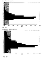
FIG. 7 is a graphical representation of the location within an ingot of samples analyzed for a solidification trial without electromagnetic stirring. -
FIGs. 8A to 8H are graphical representations for various elements of the elemental distribution as a function of the location in the ingot as depicted inFIG. 7 . -
FIG. 9 is a graphical representation of the location within an ingot of samples analyzed for a solidification trial with electromagnetic stirring. -
FIG. 10A to 10H are graphical representations for various elements of the elemental distribution as a function of the location in the ingot as depicted inFIG. 9 . - While the invention will be described in conjunction with example embodiments, it will be understood that it is not intended to limit the scope of the invention to such embodiments. On the contrary, it is intended to cover all alternatives, modifications and equivalents. The following description is to be read with reference to
FIGs. 1A to 10H . - As mentioned, the present invention relates to a process of purification by crystallization that produces medium and/or high purity silicon metal for use in photovoltaic applications.
- More specifically, in accordance with one aspect of the invention, there is provided a process for purifying low-purity metallurgical grade silicon, containing at least one of the following contaminants Al, As, Ba, Bi, Ca, Cd, Fe, Co, Cr, Cu, Fe, La, Mg, Mn, Mo, Na, Ni, P, Pb, Sb, Sc, Sn, Sr, Ti, V, Zn, Zr, and B, and obtaining a higher-purity solid polycrystalline silicon.
- The basic steps of this process are discussed more fully hereinafter with particular reference to
FIGs. 1 to 3 , andFIG. 6 . - Low-purity liquid metallurgical grade silicon is produced by carbothermal reduction of quartz in an electric arc furnace. The liquid silicon (the melt) 11 may be transferred into ladles from where it may be then outpoured into a
mould 10 having aninsulated bottom wall 10a,insulated side walls 10b, and an open top 10c. Themould 10 may have a rectangular, cylindrical, inverted-bell shape, or any other shape known to a person skilled in the art. It may also have atap 24 provided thereon (seeFIG. 1 B) . - In order to obtain a unidirectional solidification, the
side walls 10b andbottom wall 10a of the mould are insulated with an appropriate insulation, for example silica sand or some appropriate refractory lining, while the top 10c of the mould is open to allow the exposed surface of the melt to emit heat (seeFIGs. 1A and1B ). Accordingly, the solidification of the ingot along theside walls 10b and thebottom wall 10a should be negligible compared to that along the top 10c. Heating of the insulation is recommended in order to minimize the thickness of a silicon skin that may solidify and form on the walls of themould 10. - To ensure a continuous washing of the solidification interface and to dilute the concentration of impurity elements that accumulate at the solidification front, the silicon melt is stirred electromagnetically. The electromagnetic stirring may be provided by any appropriate
electromagnetic stirrer 14.FIGs. 1A ,1B ,2 ,3 , and6 show a mould with an electromagnetic stirrer placed underneath the mould. Electromagnetic stirring, unlike conventional mechanical stirring, is a non-contact stirring, i.e. no part of the actual stirrer comes into contact with the molten metal. - In order to minimize the quantity of impurity rich liquid silicon trapped by dendrite formation, the rate of unidirectional solidification must be controlled. Preferably, the rate of unidirectional solidification is less than 1x10⁴ m/s or even more preferably comprised between 1x10⁻⁴ m/s and 5x10⁻⁶ m/s.
- The rate of unidirectional solidification may be controlled by controlling the rate of heat extraction from the open top 10c of the
mould 10. It should be noted that the term "heat extraction" is understood to include heat removal and simple heat emission. This may be accomplished with the type of insulation used for the bottom and side walls as well as by placing the free surface of the melt at the open top of the mould in contact with a coolingmedium 20, such as air or water. For example, the solidification can be slowed by using a light insulation or accelerated by using a water shower to cool the exposed free surface of the melt. - When 40 to 80% of the melt has solidified, the unidirectional solidification is stopped thus obtaining an
ingot 19 having an exterior shell made of higher-purity solidpolycrystalline silicon 18 and a center made of an impurity-enrichedliquid silicon 16. Stopping the unidirectional solidification simply implies not allowing the melt to completely solidify and proceeding to the next step. - Once 40 to 80% of the melt has solidified, a crack or an
opening 22 is created in the exterior shell of theingot 19 to outflow the impurity-enrichedliquid silicon 16 from the center and leave behind the exterior shell of higher-purity solidpolycrystalline silicon 18. - The
liquid silicon 16 may be extracted from the center of theingot 19 by piercing the exterior shell of theingot 19, for example by mechanical means or thermal lance, to create anopening 22 in the exterior shell of theingot 19 through which the liquid silicon may be extracted. - The actual extraction of the
liquid silicon 16 from theingot 19 may be done by tapping the ingot through atap 24 found in the mould 10 (seeFIG. 1 B) , either in thebottom wall 10a of themould 10 or aside wall 10b. For example, a thermal lance may be used to create an opening in the exterior shell of the ingot through thetap 24 in themould 10 to outpour theliquid silicon 16. - The process may further include an additional step before step (e) of removing the
ingot 19 from the mould 10 (seeFIG. 2 ), for example by lifting theingot 19 out of themould 10 using an appropriate suspension mechanism 26 (seeFIG. 3 ). For example, in this way, while theingot 19 is suspended in mid-air, the bottom portion of theingot 19 is caused to crack, by piercing or quenching, to draw off theliquid silicon 16. - A top portion of the higher-purity solid polycrystalline silicon thus obtained may contain approximately at least 90% less of contaminants Al, As, Ba, Bi, Ca, Cd, Co, Cr, Cu, Fe, K, La, Mg, Mn, Mo, Na, Ni, Pb, Sb, Sc, Sn, Sr, Ti, V, Zn, Zr than the silicon starting material.
- The higher-purity solid polycrystalline silicon may contain approximately at least 45% less phosphorus and approximately at least 10% less boron than the metallurgical grade silicon starting material.
- Advantageously, the impurity-enriched liquid silicon may contain less than 60 ppmw of carbon and less than 20 ppmw of oxygen and thus may provide a low carbon and low oxygen grade of silicon.
- Of course, the entire process - from step (a) to (e) - may be repeated using the higher purity solid polycrystalline silicon, a so-called medium purity silicon, as starting material to thereby obtain a final silicon material of an even higher purity, a so-called high purity silicon. In this way, solar grade silicon may be obtained from metallurgical grade silicon.
- Directional solidification is a common method of purification. Metallurgical grade silicon contains a significant level of impurities which favours structural supercooling during solidification. When there is a presence of supercooling during solidification of a liquid metal, the type of solidification is dendritic, as shown in
FIG. 4 . Dendritic solidification is a very inefficient directional solidification - a certain quantity of impurity-rich liquid (L) is trapped during solidification by the dendritic arms. - With no electromagnetic agitation of the melt during solidification of the melt, 50% of the initial liquid is trapped by the dendritic arms. This gives us a purification efficiency of:


where - [El] solid : concentration of the solute in the solid metal;
- [El] liquid : concentration of the solute in the liquid metal;
- R: fraction of the impure melt trapped in the solid metal during crystallization;
- kth : segregation coefficient determined by Czochralski crystallization of silicon;
- keff : segregation coefficient determined by our new process.
- A sampling of the solidified melt of metallurgical grade silicon, taken from the surface of the ingot, yields the following information:

thus, R = 0.49 ≈ 0.50 - The constant R is valid for all elements for this particular technique.
- Some examples:


Table 1 Element keff Al 0.50 Ca 0.50 Co 0.50 Cr 0.50 Cu 0.50 Fe 0.50 Mg 0.50 Mn 0.50 Mo 0.50 Ni 0.50 P 0.68 Ti 0.50 V 0.50 Zr 0.50 B 0.90 - A purification efficiency of approximately 50% is obtained for a majority of the elements (except boron and phosphorus). In fact, about 30% of the phosphorus and 10% of boron can be removed by our technique of large mould segregation by directional solidification without electromagnetic stirring.
- The partition (segregation) coefficient (keff ) stays the same during solidification however the composition of the liquid at equilibrium with the solid increases in solute content. The Scheil equation describes well this phenomenon.
- The composition of the solid at the solidification interface is, according to the Scheil equation (diffusion and convection in the liquid, no diffusion in the solid):

- Cs : Concentration of the solute in the solid;
- Co : Initial concentration of the solute in the liquid;
- k: Segregation coefficient;
- fs : Solid fraction.
- Therefore, if the solidification is stopped at a specific moment and an analysis of the solid on average is carried out, the average concentration of the solute in the solid portion is:


- A graphical representation of the above equation is given in
FIG. 5 . - It is worth noting that depending on the solid fraction, the average efficiency of the purification is affected. The first solid formed is the most pure. When the solidification is stopped and a global chemical analysis of the solid is performed, the efficiency is slightly lower because of the increase in the concentration of the liquid in solute. This explains well the experimental results observed after complete solidification of a silicon ingot (but only the layer solidified from the upper surface of the ingot).
- It is noted that when solidification is carried out without agitation of the liquid (melt), the lower part of the ingot is typically richer in impurities than the upper part. An explanation for this could possibly be found in the difference in densities between the (cooler) impurity-rich liquid and that of the center of the ingot: the composition of the liquid is not homogeneous.
- When the melt is only partially solidified, the liquid may be separated from the solid by creating an opening or a crack in the shell for example by piercing the shell of the ingot (for example: by thermal lance, mechanical piercing, or other). The opening or crack may be obtained by solidifying the silicon in a mould provided with a closable outlet in the bottom portion. Once the liquid has solidified to the required degree, the outlet is opened and the shell pierced to draw off the liquid. As shown in the embodiments of
FIGs 1 to 3 , the opening or crack can also be obtained by lifting up the shell from the mould with an appropriate suspension system. While the shell is in suspension in the air, the bottom portion is caused to crack by piercing or quenching to draw off the liquid. The ingot could also be completely solidified so as to then remove the portions that are of interest chemically. The mould may have a rectangular or cylindrical shape. It could also have the shape of upside down bell or any other shape known to a person skilled in the art. (SeeFIGs. 1 to 3 ) - The final silicon solid contains fewer impurities (i.e. is depleted of impurities) while the liquid at the center of the ingot is enriched in impurities.
- We want to obtain the concentration of iron in the solid and in the liquid upon solidification of 70% of the silicon melt (time of solidification: 4.5 hours). The quantity of liquid silicon is 5.0 mt and the composition of the liquid silicon includes 0.35% Fe.


obtained fromFIG. 5 . - By taking into account the mass distribution we obtain:


- Therefore, after treatment, we obtain:
- ⇒ 3.5 mt of solid silicon at 0.23 %Fe
- ⇒ 1.5 mt of liquid silicon at 0.64 %Fe
- During solidification, the dendrites trap impurity-rich liquid coming from a diffusion layer at the solid/liquid interface.
- To minimize the presence of dendrites, a planar solidification front may be promoted. A certain quantity of solute may be trapped with planar solidification, but this quantity is far less than that trapped during dendritic solidification. A planar directional solidification may be promoted by allowing heat to escape from a single surface of the ingot.
- In addition, to homogenize the impurity-rich liquid and break down the diffusion layer at the solid/liquid interface, the liquid should preferably be agitated, stirred.
- In order to obtain a substantially polycrystalline unidirectional solidification, the walls of the mould may be insulated (as shown in
FIGs. 1 to 3 ) while the top may be open to allow heat to be emitted therefrom (the solidification of the melt can be slowed by a light insulation or accelerated by a water shower). Accordingly, the solidification along the walls and the bottom should be negligible compared to that along the top of the ingot (heating of the insulation is recommended in order to minimize the thickness of the silicon skin solidified on the walls of the mould). - The present invention involves the use of an electromagnetic stirrer. Electromagnetic stirrers are known for stirring molten metal. For example, they are used to stir aluminum as it melts in a furnace. The electromagnetic stirrer utilizes the principle of a linear motor and differs from the conventional mechanical and decompression types as it is a non-contact stirrer in which no part touches the molten metal (see
FIG. 6 ). - As shown in
FIG. 6 , a coil installed at the bottom of the mould generates a moving magnetic field (H) when a 3-phase AC voltage is applied to this coil (inductor). Electric power force is generated in the molten metal due to the action of the magnetic field (magnetic flux) and causes induction current (I) to flow. This current then acts with the magnetic field of the inductor to induce electromagnetic force (F) in the molten metal. As this thrust moves in the direction of the moving magnetic field, the molten metal also moves. In other words, a stirring action is applied. Furthermore, as this thrust has components in the horizontal direction and in the vertical direction, the molten metal flows diagonally upwards resulting in a uniform temperature and chemical composition in both the top and bottom layers of the molten metal. - The speed of the solidification interface is fixed by the rate of heat loss. For a surface without insulation (the upper portion of the ingot) the thickness of the solid silicon and the rate of solidification in ambient air are (from experiment):


where E is the thickess of the top solid layer of the ingot, v is the rate of solidification at the interface, and t is the total time of solidification. - A control experiment was carried out: unidirectional solidification in an insulated mould without electromagnetic stirring of the melt during solidification.
- A sample was taken from the center of the ingot, according to the diagram shown in
FIG. 7 , and analyzed the results are given hereinbelow in Table 2. A graphical representation of the elemental impurity distribution in the ingot as a function of position in the ingot of several of the elements is shown inFIGs. 8A to 8H .Table 2. Liq. 1 2 3 4 5 6 7 8 9 10 11 12 13 14 15 16 17 18 Al 0.3028 0.1689 0.1641 0.1290 0.1397 0.1476 0.1295 0.3336 0.5828 0.1969 0.2420 0.4253 0.5233 0.4394 0.2552 0.2826 0.2858 0.4562 1.6030 AS 0.0050 0.0030 0.0029 0.0025 0.0024 0.0029 0.0028 0.0038 0.0044 0.0037 0.0046 0.0078 0.0097 0.0084 0.0047 0.0044 0.0053 0.0174 0.0299 Ba 0.0011 0.0005 0.0005 0.0003 0.0005 0.0005 0.0003 0.0031 0.0084 0.0005 0.0006 0.0010 0.0012 0.0011 0.0006 0.0012 0.0013 0.0023 0.0089 Bi 0.0002 0.0003 0.0002 0.0002 0.0002 0.0001 0.0002 0.0003 0.0004 0.0003 0.0004 0.0006 0.0009 0.0009 0.0005 0.0004 0.0005 0.0016 0.0025 Ca 0.0742 0.0313 0.0321 0.0211 0.0317 0.0299 0.0187 0.2393 0.6633 0.0258 0.0314 0.0550 0.0672 0.0572 0.0334 0.0893 0.0882 0.1806 0.4187 Cd 0.0001 0.0001 0.0001 0.0001 0.0001 0.0001 0.0001 0.0001 0.0001 0.0001 0.0001 0.0001 0.0001 0.0001 0.0001 0.0001 0.0001 0.0001 0.0001 Co 0.0007 0.0006 0.0006 0.0005 0.0005 0.0005 0.0005 0.0006 0.0008 0.0006 0.0007 0.0012 0.0012 0.0010 0.0008 0.0007 0.0008 0.0021 0.0032 Cr 0.0037 0.0025 0.0022 0.0023 0.0018 0.0020 0.0020 0.0026 0.0030 0.0027 0.0034 0.0057 0.0070 0.0059 0.0035 0.0033 0.0040 0.0131 0.0209 Cu 0.0043 0.0027 0.0025 0.0020 0.0021 0.0023 0.0021 0.0031 0.0034 0.0032 0.0040 0.0071 0.0088 0.0074 0.0042 0.0038 0.0046 0.0165 0.0278 Fe 1.3665 0.8744 0.8224 0.6788 0.6707 0.7498 0.6853 0.9783 1.0696 1.0273 1.2536 2.1771 2.7017 2.2976 1.3181 1.2426 1.5025 5.1867 8.5841 La 0.0033 0.0021 0.0020 0.0017 0.0017 0.0019 0.0017 0.0026 0.0034 0.0025 0.0029 0.0050 0.0061 0.0052 0.0038 0.0030 0.0036 0.0123 0.0190 Mg 0.0010 0.0005 0.0005 0.0004 0.0004 0.0005 0.0004 0.0012 0.0026 0.0007 0.0008 0.0014 0.0015 0.0014 0.0008 0.0009 0.0012 0.0063 0.0170 Mn 0.0238 0.0174 0.0141 0.0117 0.0116 0.0136 0.0118 0.0168 0.0197 0.0181 0.0232 0.0386 0.0483 0.0405 0.0236 0.0226 0.0264 0.0930 0.1550 Mo 0.0012 0.0015 0.0020 0.0005 0.0009 0.0015 0.0013 0.0010 0.0019 0.0010 0.0010 0.0013 0.0012 0.0012 0.0011 0.0010 0.0005 0.0022 0.0029 Na 0.0001 0.0001 0.0001 0.0001 0.0001 0.0001 0.0001 0.0001 0.0001 0.0001 0.0001 0.0001 0.0001 0.0001 0.0001 0.0001 0.0001 0.0097 0.0915 Ni 0.0024 0.0015 0.0015 0.0015 0.0012 0.0013 0.0012 0.0016 0.0019 0.0018 0.0022 0.0037 0.0046 0.0038 0.0023 0.0021 0.0025 0.0093 0.0145 P 0.0047 0.0034 0.0039 0.0038 0.0033 0.0032 0.0032 0.0039 0.0045 0.0049 0.0061 0.0082 0.0084 0.0078 0.0053 0.0046 0.0047 0.0077 0.0121 Pb 0.0007 0.0004 0.0003 0.0005 0.0006 0.0002 0.0004 0.0004 0.0006 0.0004 0.0002 0.0005 0.0005 0.0004 0.0004 0.0003 0.0005 0.0009 0.0014 Sb 0.0028 0.0018 0.0015 0.0012 0.0014 0.0014 0.0013 0.0029 0.0042 0.0021 0.0023 0.0042 0.0050 0.0043 0.0027 0.0024 0.0029 0.0064 0.0148 Sc 0.0001 0.0001 0.0001 0.0001 0.0001 0.0001 0.0001 0.0001 0.0002 0.0001 0.0001 0.0002 0.0002 0.0002 0.0001 0.0001 0.0002 0.0005 0.0009 Sn 0.0006 0.0001 0.0005 0.0008 0.0002 0.0001 0.0006 0.0003 0.0007 0.0004 0.0005 0.0001 0.0006 0.0009 0.0004 0.0001 0.0005 0.0008 0.0004 Sr 0.0008 0.0003 0.0003 0.0002 0.0003 0.0003 0.0002 0.0027 0.0078 0.0002 0.0003 0.0006 0.0007 0.0006 0.0003 0.0009 0.0010 0.0020 0.0049 Ti 0.0893 0.0554 0.0536 0.0432 0.0433 0.0482 0.0440 0.0627 0.0695 0.0663 0.0811 0.1435 0.1762 0.1493 0.0848 0.0797 0.0997 0.3386 0.5625 V 0.0018 0.0011 0.0011 0.0009 0.0009 0.0010 0.0009 0.0013 0.0015 0.0013 0.0016 0.0028 0.0035 0.0029 0.0017 0.0016 0.0020 0.0078 0.0126 Zn 0.0006 0.0004 0.0004 0.0003 0.0003 0.0003 0.0003 0.0008 0.0005 0.0005 0.0004 0.0008 0.0010 0.0009 0.0005 0.0005 0.0006 0.0016 0.0031 Zr 0.0177 0.0112 0.0108 0.0089 0.0088 0.0098 0.0090 0.0125 0.0136 0.0133 0.0162 0.0279 0.0341 0.0289 0.0168 0.0159 0.0197 0.0648 0.0987 B 0.0039 0.0036 0.0036 0.0036 0.0036 0.0035 0.0036 0.0038 0.0041 0.0042 0.0045 0.0048 0.0050 0.0047 0.0044 0.0045 0.0044 0.0031 0.0024 - A sampling of the silicon at surface of the ingot yields the following information:


so, R = 0.50 - The purification efficiency should be:


Table 3 Element Theory keff Experimental keff Al 0.50 0.46 Ca 0.50 0.43 Co 0.50 0.43 Cr 0.50 0.71 Cu 0.50 0.49 Fe 0.50 0.49 Mg 0.50 0.49 Mn 0.50 0.49 Mo 0.50 0.75 Ni 0.50 0.50 P 0.68 0.70 Ti 0.50 0.48 V 0.50 0.50 Zr 0.50 0.50 B 0.90 0.92 - Experimental results show that about 50% of most of the elements may be removed from the upper part of the silicon ingot. This type of solidification may also remove about 30% of phosphorus and about 10% of boron from the upper part of the silicon ingot.
- As seen in the graphs of
FIGs. 8A to 8H , the more cool impurity-rich liquid silicon which is more dense accumulates at the bottom of the liquid found at the center of the ingot where it may be trapped by dendrite formation at the bottom of the ingot. - An experiment was carried out: unidirectional solidification in an insulated mould with electromagnetic stirring of the melt during solidification.
- A sample was taken from the center of the ingot, according to the diagram shown in
FIG. 9 , and analyzed the results are given hereinbelow in Table 4. A graphical representation of the elemental impurity distribution in the ingot as a function of position in the ingot of several of the elements is shown inFIGs. 10A to 10H .
- Electromagnetic agitation had a large effect on the distribution of impurities in the silicon ingot. The agitation prevented the separation of impurities towards the bottom of the silicon ingot. Moreover, there was a large increase in the segregation of impurities (the surface layer is much more pure).
- A sampling of the silicon at surface of the ingot yields the following information:


so, R = 0.017 ≈ 0.02 - In theory, the efficiency of the purification is:


Table 5 Element Theory keff Experimental keff Al 0.02 0.01 Ca 0.02 0.18 Co 0.02 --- Cr 0.02 0.07 Cu 0.02 --- Fe 0.02 0.02 Mg 0.02 --- Mn 0.02 0.16 Mo 0.02 --- Ni 0.02 0.05 P 0.36 0.39 Ti 0.02 0.01 V 0.02 --- Zr 0.02 --- B 0.80 0.79 - These results show that we can expect to obtain a very pure layer (approximately 30 cm thick at the top surface of the ingot) upon partial solidification of the silicon melt. This should correspond to a solidification time of approximately 4.5 hours with air-cooling at the open top of the ingot.
- The experiments conducted showed that the ingot obtained with agitation of the melt during solidification of the melt developed a lot more cracks than the ingot obtained without agitation of the melt during solidification of the melt. Each crack can lead to a small amount of contamination caused by an intrusion of impure metal into the "purified" zone. However, this cracking should be lessened by not solidifying completely the melt.
- A more homogeneous liquid is obtained with electromagnetic agitation (i.e., electromagnetic stirring) of the melt during solidification of the melt.
- According to the results obtained, this procedure may be capable of removing more than 50% of phosphorus and makes the method very interesting for the production of Solar Grade silicon from Metallurgic Grade silicon.
- The solidification speed may range between 10-6 m/s and 10-4 m/s. High solidification speeds may be achieved with this method as compared with other crystallization methods. This provides a cost effective solution for mass production of high-purity silicon.
- The outer layer (first skin of silicon) of the ingot freezes rapidly, relieving the heat in excess. Then the temperature of the liquid silicon drops to approximately 1410°C. At this moment, we obtain the minimum solubility values for carbon and oxygen.
- Analytical results of the liquid center of the ingot confirm a carbon content of less than 60 ppmw and an oxygen content of less than 20 ppmw. Analysis done by an external laboratory confirmed a carbon content of less than 20 ppmw and an oxygen content of less than 20 ppmw. Advantageously, we have now a new process that produces a grade of silicon with low-carbon and low-oxygen content.
Claims (17)
- A process for purifying low-purity metallurgical grade silicon, containing at least one of the following contaminants Al, As, Ba, Bi, Ca, Cd, Fe, Co, Cr, Cu, Fe, La, Mg, Mn, Mo, Na, Ni, P, Pb, Sb, Sc, Sn, Sr, Ti, V, Zn, Zr, and B, and obtaining a higher-purity solid polycrystalline silicon, said process comprising the steps of:(a) containing a melt of low-purity metallurgical grade silicon in a mould, said mould having an insulated bottom wall, insulated side walls, and an open top;(b) solidifying the melt by unidirectional solidification from said open top towards said insulated bottom wall of said mould while electromagnetically stirring the melt;(c) controlling a rate of said unidirectional solidification;(d) stopping said unidirectional solidification when the melt has partially solidified to produce an ingot having an exterior shell comprising said higher-purity solid polycrystalline silicon and a center comprising an impurity-enriched liquid silicon; and(e) creating an opening in said exterior shell of said ingot to outflow said impurity-enriched liquid silicon and leave the exterior shell comprising said higher-purity solid polycrystalline silicon thereby obtaining said higher-purity solid polycrystalline silicon.
- A process according to claim 1, wherein said insulated bottom wall and said insulated side walls are heated to minimize a formation of a skin of silicon on said insulated bottom wall and said insulated side walls of said mould.
- A process according to claim 1, wherein said rate of unidirectional solidification is controlled by an insulation of said insulated bottom wall and said insulated side walls.
- A process according to claim 1, wherein said rate of unidirectional solidification is controlled by controlling a rate of heat extraction from the melt at said open top of said mould.
- A process according to claim 4, wherein said controlling a rate of heat extraction comprises placing a cooling medium in contact with a free surface of the melt at said open top of said mould.
- A process according to claim 5, wherein said cooling medium is water or air.
- A process according to claim 1, wherein said rate of unidirectional solidification is determined so as to minimize dendrite formation.
- A process according to claim 7, wherein said rate of unidirectional solidification is less than 1x10⁻⁴ m/s.
- A process according to claim 7, wherein said rate of unidirectional solidification is comprised between 1x10⁻⁴ m/s and 5x10⁻⁶ m/s.
- A process according to claim 1, wherein said stopping the unidirectional solidification is done when 40 to 80% of the melt has solidified.
- A process according to claim 1, wherein said creating an opening in said exterior shell of said ingot of step (e) comprises piercing said exterior shell of said ingot by mechanical means or thermal lance.
- A process according to claim 1, wherein said creating an opening in said exterior shell of said ingot of step (e) is accomplished through a tap opening in said mould.
- A process according to claim 1, wherein said process further comprises an additional step before step (e) of removing said ingot from said mould.
- A process according to claim 1, wherein said process further comprises an additional step (f) of melting said higher-purity solid polycrystalline silicon and repeating steps (b) to (e).
- A process according to claim 1, wherein a top portion of said higher-purity solid polycrystalline silicon contains at least 90% less metal contaminants Al, As, Ba, Bi, Ca, Cd, Co, Cr, Cu, Fe, K, La, Mg, Mn, Mo, Na, Ni, Pb, Sb, Sc, Sn, Sr, Ti, V, Zn, and Zr than the low-purity metallurgical grade silicon.
- A process according to claim 1, wherein said higher-purity solid polycrystalline silicon contains approximately at least 45% less phosphorus and approximately at least 10% less boron than the low-purity metallurgical grade silicon.
- A process according to claim 1, wherein said impurity-enriched liquid silicon contains less than 60 ppm of carbon and less than 20 ppm of oxygen and is a low carbon and low oxygen grade of silicon.
Applications Claiming Priority (2)
| Application Number | Priority Date | Filing Date | Title |
|---|---|---|---|
| US96006107P | 2007-09-13 | 2007-09-13 | |
| PCT/CA2008/000492 WO2009033255A1 (en) | 2007-09-13 | 2008-03-13 | Process for the production of medium and high purity silicon from metallurgical grade silicon |
Publications (3)
| Publication Number | Publication Date |
|---|---|
| EP2212249A1 EP2212249A1 (en) | 2010-08-04 |
| EP2212249A4 EP2212249A4 (en) | 2012-08-15 |
| EP2212249B1 true EP2212249B1 (en) | 2015-01-14 |
Family
ID=40451503
Family Applications (1)
| Application Number | Title | Priority Date | Filing Date |
|---|---|---|---|
| EP08733596.4A Active EP2212249B1 (en) | 2007-09-13 | 2008-03-13 | Process for the production of medium and high purity silicon from metallurgical grade silicon |
Country Status (16)
| Country | Link |
|---|---|
| US (1) | US7727502B2 (en) |
| EP (1) | EP2212249B1 (en) |
| JP (1) | JP2010538952A (en) |
| KR (1) | KR20100061510A (en) |
| CN (1) | CN101868422B (en) |
| AU (1) | AU2008299523A1 (en) |
| BR (1) | BRPI0816972A2 (en) |
| CA (1) | CA2695393C (en) |
| EA (1) | EA017480B1 (en) |
| ES (1) | ES2530720T3 (en) |
| MX (1) | MX2010002728A (en) |
| MY (1) | MY143807A (en) |
| NO (1) | NO20100512L (en) |
| UA (1) | UA97691C2 (en) |
| WO (1) | WO2009033255A1 (en) |
| ZA (1) | ZA201000882B (en) |
Families Citing this family (15)
| Publication number | Priority date | Publication date | Assignee | Title |
|---|---|---|---|---|
| JPWO2008149985A1 (en) * | 2007-06-08 | 2010-08-26 | 信越化学工業株式会社 | Solidification method of metallic silicon |
| JP4748187B2 (en) * | 2007-12-27 | 2011-08-17 | 国立大学法人東北大学 | Method for producing Si crystal ingot |
| CN103154288A (en) | 2010-05-20 | 2013-06-12 | 道康宁公司 | Method and system for producing an aluminum-silicon alloy |
| JP2012106886A (en) * | 2010-11-17 | 2012-06-07 | Nippon Steel Materials Co Ltd | Method and apparatus for solidification refining metallic silicon |
| CN102275931B (en) * | 2011-07-05 | 2013-05-29 | 兰州大学 | Method for Purifying Metallurgical Grade Polysilicon Powder by Oxyhydrogen Flame Plasma |
| WO2013010575A1 (en) * | 2011-07-18 | 2013-01-24 | Abb Research Ltd | A method and a control system for controlling a melting process |
| CN103266350B (en) * | 2013-05-31 | 2015-08-12 | 大连理工大学 | Polycrystalline silicon ingot silicon vacuum solid-liquid separation method and separation equipment |
| CN103266349B (en) * | 2013-05-31 | 2015-07-15 | 大连理工大学 | High-purity hollow silicon material, polycrystalline silicon ingot silicon vacuum solid-liquid separation method and equipment |
| JP6401051B2 (en) * | 2014-12-26 | 2018-10-03 | 京セラ株式会社 | Method for producing polycrystalline silicon ingot |
| RU2632827C2 (en) * | 2015-12-08 | 2017-10-10 | Общество с ограниченной ответственностью "Современные химические и металлургические технологии" (ООО "СХИМТ") | Device for refining silicon |
| CN107255572B (en) * | 2017-05-12 | 2020-04-21 | 宜昌南玻硅材料有限公司 | Minority carrier lifetime sampling method of silicon ingot in semi-molten ingot casting process |
| JP6919633B2 (en) | 2018-08-29 | 2021-08-18 | 信越半導体株式会社 | Single crystal growth method |
| CN113412237B (en) * | 2019-04-30 | 2024-06-07 | 瓦克化学股份公司 | Method for refining crude silicon melt using granular media |
| CN111675222B (en) * | 2020-07-13 | 2022-08-09 | 昆明理工大学 | Method for producing industrial silicon by using low-grade silica |
| EP4082966A1 (en) | 2021-04-26 | 2022-11-02 | Ferroglobe Innovation, S.L. | Method for obtaining purified silicon metal |
Family Cites Families (59)
| Publication number | Priority date | Publication date | Assignee | Title |
|---|---|---|---|---|
| US2890139A (en) * | 1956-12-10 | 1959-06-09 | Shockley William | Semi-conductive material purification method and apparatus |
| US3012865A (en) * | 1957-11-25 | 1961-12-12 | Du Pont | Silicon purification process |
| US3752221A (en) * | 1969-10-30 | 1973-08-14 | United Aircraft Corp | Mold apparatus for casting with downward unidirectional solidification |
| US4094731A (en) * | 1976-06-21 | 1978-06-13 | Interlake, Inc. | Method of purifying silicon |
| US4298423A (en) * | 1976-12-16 | 1981-11-03 | Semix Incorporated | Method of purifying silicon |
| US4200621A (en) * | 1978-07-18 | 1980-04-29 | Motorola, Inc. | Sequential purification and crystal growth |
| US4242175A (en) * | 1978-12-26 | 1980-12-30 | Zumbrunnen Allen D | Silicon refining process |
| SE448164B (en) * | 1979-05-24 | 1987-01-26 | Aluminum Co Of America | PROCEDURE FOR PROVIDING A BED OF PURE SILICONE CRYSTALS |
| US4304703A (en) * | 1980-06-23 | 1981-12-08 | Ppg Industries, Inc. | Cationic polymer dispersions and their method of preparation |
| DE3150539A1 (en) | 1981-12-21 | 1983-06-30 | Siemens AG, 1000 Berlin und 8000 München | Process for producing silicon which can be used for semiconductor components, in particular for solar cells |
| FR2524489A1 (en) * | 1982-03-30 | 1983-10-07 | Pechiney Aluminium | PROCESS FOR PURIFYING METALS BY SEGREGATION |
| DE3220285A1 (en) | 1982-05-28 | 1983-12-01 | Siemens AG, 1000 Berlin und 8000 München | METHOD FOR PRODUCING POLYCRYSTALLINE, SUITABLE FOR SUBSEQUENT ZONE MELTING |
| NO152551C (en) * | 1983-02-07 | 1985-10-16 | Elkem As | PROCEDURE FOR THE PREPARATION OF PURE SILICONE. |
| DE3310827A1 (en) * | 1983-03-24 | 1984-09-27 | Bayer Ag, 5090 Leverkusen | METHOD FOR PRODUCING COARSE CRYSTALLINE SILICON |
| DE3323896A1 (en) | 1983-07-02 | 1985-01-17 | Leybold-Heraeus GmbH, 5000 Köln | Process and apparatus for the directed solidification of melts |
| JPH0753569B2 (en) * | 1986-08-07 | 1995-06-07 | 昭和アルミニウム株式会社 | Silicon purification method |
| JPH0696444B2 (en) | 1987-08-27 | 1994-11-30 | 川崎製鉄株式会社 | Method for producing high-purity silicon |
| DE3802531A1 (en) | 1988-01-28 | 1989-08-17 | Siemens Ag | METHOD FOR SEPARATING SOLID PARTICLES FROM MELTIC MELT |
| DE3804248A1 (en) | 1988-02-11 | 1989-08-24 | Siemens Ag | METHOD FOR SEPARATING IMPURITIES FROM A SILICONE MELT BY DIRECTIONALIZATION |
| DE3929635A1 (en) | 1989-09-06 | 1991-03-07 | Siemens Ag | Solid particle sepn. from silicon melt - by time-variable crucible rotation during directional solidification |
| JPH05124809A (en) | 1991-10-30 | 1993-05-21 | Nippon Sheet Glass Co Ltd | Solidification refining method of silicon |
| JP3263104B2 (en) | 1991-11-27 | 2002-03-04 | 川崎製鉄株式会社 | Purification method of metallic silicon |
| JPH05254817A (en) | 1992-03-12 | 1993-10-05 | Kawasaki Steel Corp | Production of polycrystal silicon ingot |
| WO1997003922A1 (en) | 1994-01-10 | 1997-02-06 | Showa Aluminum Corporation | Process for producing high-purity silicon |
| JP3140300B2 (en) | 1994-03-29 | 2001-03-05 | 川崎製鉄株式会社 | Method and apparatus for purifying silicon |
| NO180532C (en) * | 1994-09-01 | 1997-05-07 | Elkem Materials | Process for removing contaminants from molten silicon |
| JPH0873297A (en) | 1994-09-05 | 1996-03-19 | Shin Etsu Chem Co Ltd | Substrate material for solar cell and solar cell using the same |
| JPH08217436A (en) | 1995-02-17 | 1996-08-27 | Kawasaki Steel Corp | Solidification and purification of metal silicon, device therefor, and mold used for the device |
| EP0757013B1 (en) * | 1995-08-04 | 2001-11-07 | Sharp Kabushiki Kaisha | Apparatus for purifying metal |
| KR100263220B1 (en) * | 1996-10-14 | 2000-09-01 | 에모토 간지 | Method and apparatus for manufacturing polycrystalline silicon and method for manufacturing silicon substrate for solar cell |
| JPH10139415A (en) | 1996-10-30 | 1998-05-26 | Kawasaki Steel Corp | Solidification and purification of molten silicon |
| JPH10182135A (en) | 1996-12-20 | 1998-07-07 | Kawasaki Steel Corp | Solidification refining of silicon |
| JPH10182137A (en) | 1996-12-26 | 1998-07-07 | Kawasaki Steel Corp | Solidifying purification of silicon for solar cell and apparatus therefor |
| JPH10182286A (en) | 1996-12-26 | 1998-07-07 | Kawasaki Steel Corp | Continuous casting method of silicon |
| JPH10182129A (en) | 1996-12-26 | 1998-07-07 | Kawasaki Steel Corp | Refining of metal silicon |
| JP3852147B2 (en) | 1996-12-27 | 2006-11-29 | Jfeスチール株式会社 | Method for producing polycrystalline silicon ingot for solar cell |
| JPH10251008A (en) | 1997-03-14 | 1998-09-22 | Kawasaki Steel Corp | Method for solidifying and refining metal silicon |
| JPH10251009A (en) | 1997-03-14 | 1998-09-22 | Kawasaki Steel Corp | Method for solidifying and refining silicon for solar battery |
| CA2232777C (en) * | 1997-03-24 | 2001-05-15 | Hiroyuki Baba | Method for producing silicon for use in solar cells |
| JPH10273313A (en) | 1997-03-28 | 1998-10-13 | Kawasaki Steel Corp | Production of polycrystal silicon ingot |
| JPH10273311A (en) | 1997-03-28 | 1998-10-13 | Kawasaki Steel Corp | Purification of silicon for solar battery and apparatus therefor |
| JP3520957B2 (en) * | 1997-06-23 | 2004-04-19 | シャープ株式会社 | Method and apparatus for manufacturing polycrystalline semiconductor ingot |
| JP3523986B2 (en) * | 1997-07-02 | 2004-04-26 | シャープ株式会社 | Method and apparatus for manufacturing polycrystalline semiconductor |
| US5972107A (en) * | 1997-08-28 | 1999-10-26 | Crystal Systems, Inc. | Method for purifying silicon |
| JP4003271B2 (en) | 1998-01-12 | 2007-11-07 | Jfeスチール株式会社 | Silicon unidirectional solidification equipment |
| JPH11310496A (en) * | 1998-02-25 | 1999-11-09 | Mitsubishi Materials Corp | Production of silicon ingot having unidirectionally solidified texture and apparatus therefor |
| JP4365480B2 (en) | 1999-06-07 | 2009-11-18 | 昭和電工株式会社 | Manufacturing method of high purity silicon |
| JP2001278613A (en) | 2000-03-29 | 2001-10-10 | Kawasaki Steel Corp | Apparatus for unidirectional congelation of silicon |
| FR2827592B1 (en) * | 2001-07-23 | 2003-08-22 | Invensil | HIGH PURITY METALLURGICAL SILICON AND PROCESS FOR PRODUCING THE SAME |
| FR2831881B1 (en) | 2001-11-02 | 2004-01-16 | Hubert Lauvray | PROCESS FOR THE PURIFICATION OF METALLURGICAL SILICON BY INDUCTIVE PLASMA COUPLED TO DIRECTIONAL SOLIDIFICATION AND DIRECT OBTAINING OF SOLAR QUALITY SILICON |
| JP2003238137A (en) | 2002-02-21 | 2003-08-27 | Kawatetsu Techno Res Corp | Method of producing polycrystal silicon for solar cell |
| NO318092B1 (en) | 2002-05-22 | 2005-01-31 | Elkem Materials | Calcium-silicate-based slag, process for the preparation of calcium-silicate-based slag, and application for slag treatment of molten silicon |
| WO2004030044A2 (en) * | 2002-09-27 | 2004-04-08 | Astropower, Inc. | Methods and systems for purifying elements |
| CN1221470C (en) | 2002-11-26 | 2005-10-05 | 郑智雄 | High purity silicon and productive method thereof |
| CN1299983C (en) | 2003-07-22 | 2007-02-14 | 龚炳生 | Method of manufacturing a photovoltaic silicon |
| US20070202029A1 (en) | 2003-12-04 | 2007-08-30 | Gary Burns | Method Of Removing Impurities From Metallurgical Grade Silicon To Produce Solar Grade Silicon |
| NO333319B1 (en) | 2003-12-29 | 2013-05-06 | Elkem As | Silicon material for the production of solar cells |
| JP4115432B2 (en) | 2004-07-14 | 2008-07-09 | シャープ株式会社 | Metal purification method |
| MX2009002808A (en) * | 2006-09-14 | 2009-03-31 | Silicium Becancour Inc | Process and apparatus for purifying low-grade silicon material. |
-
2008
- 2008-03-13 ES ES08733596T patent/ES2530720T3/en active Active
- 2008-03-13 KR KR1020107006648A patent/KR20100061510A/en not_active Application Discontinuation
- 2008-03-13 WO PCT/CA2008/000492 patent/WO2009033255A1/en active Application Filing
- 2008-03-13 EA EA201070358A patent/EA017480B1/en not_active IP Right Cessation
- 2008-03-13 AU AU2008299523A patent/AU2008299523A1/en not_active Abandoned
- 2008-03-13 JP JP2010524312A patent/JP2010538952A/en not_active Withdrawn
- 2008-03-13 MX MX2010002728A patent/MX2010002728A/en active IP Right Grant
- 2008-03-13 UA UAA201004264A patent/UA97691C2/en unknown
- 2008-03-13 EP EP08733596.4A patent/EP2212249B1/en active Active
- 2008-03-13 US US12/047,913 patent/US7727502B2/en active Active
- 2008-03-13 CN CN200880106298.7A patent/CN101868422B/en active Active
- 2008-03-13 CA CA2695393A patent/CA2695393C/en active Active
- 2008-03-13 MY MYPI2010000616A patent/MY143807A/en unknown
- 2008-03-13 BR BRPI0816972 patent/BRPI0816972A2/en not_active IP Right Cessation
-
2010
- 2010-02-05 ZA ZA2010/00882A patent/ZA201000882B/en unknown
- 2010-04-08 NO NO20100512A patent/NO20100512L/en not_active Application Discontinuation
Also Published As
| Publication number | Publication date |
|---|---|
| CN101868422B (en) | 2013-10-09 |
| US20090074648A1 (en) | 2009-03-19 |
| UA97691C2 (en) | 2012-03-12 |
| EA017480B1 (en) | 2012-12-28 |
| MX2010002728A (en) | 2010-08-02 |
| EP2212249A4 (en) | 2012-08-15 |
| NO20100512L (en) | 2010-04-08 |
| AU2008299523A1 (en) | 2009-03-19 |
| CA2695393A1 (en) | 2009-03-19 |
| ZA201000882B (en) | 2011-04-28 |
| EA201070358A1 (en) | 2010-08-30 |
| CA2695393C (en) | 2012-01-03 |
| JP2010538952A (en) | 2010-12-16 |
| WO2009033255A1 (en) | 2009-03-19 |
| KR20100061510A (en) | 2010-06-07 |
| BRPI0816972A2 (en) | 2015-03-24 |
| CN101868422A (en) | 2010-10-20 |
| US7727502B2 (en) | 2010-06-01 |
| ES2530720T3 (en) | 2015-03-04 |
| EP2212249A1 (en) | 2010-08-04 |
| MY143807A (en) | 2011-07-15 |
Similar Documents
| Publication | Publication Date | Title |
|---|---|---|
| EP2212249B1 (en) | Process for the production of medium and high purity silicon from metallurgical grade silicon | |
| CN101423220B (en) | Method for purifying and ingot casting multi-temperature zones silicon material and apparatus thereof | |
| US7858063B2 (en) | High purity metallurgical silicon and method for preparing same | |
| US7682585B2 (en) | Silicon refining process | |
| Wu et al. | Boron removal from silicon using secondary refining techniques by metallurgical method | |
| Li et al. | Si purity control and separation from Si–Al alloy melt with Zn addition | |
| US4312849A (en) | Phosphorous removal in silicon purification | |
| CN1873062A (en) | Method for preparing polysilicon in high purity in use for solar cell | |
| Wang et al. | Control of silicon solidification and the impurities from an Al–Si melt | |
| WO2013111314A1 (en) | Silicon purification method | |
| CA1130985A (en) | Silicon purification method | |
| He et al. | A review of the process on the purification of metallurgical grade silicon by solvent refining | |
| US4246249A (en) | Silicon purification process | |
| US4312848A (en) | Boron removal in silicon purification | |
| US20100178195A1 (en) | Method of solidifying metallic silicon | |
| US4312847A (en) | Silicon purification system | |
| CN104071790B (en) | Electromagnetic agitation silicon alloy melt silicon purifying plant and method | |
| Li et al. | Bulk Si production from Si–Fe melts by directional-solidification, part II: Element distribution | |
| US4312846A (en) | Method of silicon purification | |
| Li et al. | Slag refining for separation of SiC inclusions from Si | |
| US9352970B2 (en) | Method for producing silicon for solar cells by metallurgical refining process | |
| Curtolo et al. | High-and Ultra-High-Purity Aluminum, a Review on Technical Production Methodologies. Metals 2021, 11, 1407 | |
| EP4082966A1 (en) | Method for obtaining purified silicon metal | |
| Pizzini | Solar grade silicon production from MG-Silicon | |
| Delannoy et al. | Electromagnetic Processing of Materials at SIMaP: focus on Solar Silicon elaboration |
Legal Events
| Date | Code | Title | Description |
|---|---|---|---|
| PUAI | Public reference made under article 153(3) epc to a published international application that has entered the european phase |
Free format text: ORIGINAL CODE: 0009012 |
|
| 17P | Request for examination filed |
Effective date: 20100408 |
|
| AK | Designated contracting states |
Kind code of ref document: A1 Designated state(s): AT BE BG CH CY CZ DE DK EE ES FI FR GB GR HR HU IE IS IT LI LT LU LV MC MT NL NO PL PT RO SE SI SK TR |
|
| AX | Request for extension of the european patent |
Extension state: AL BA MK RS |
|
| DAX | Request for extension of the european patent (deleted) | ||
| A4 | Supplementary search report drawn up and despatched |
Effective date: 20120712 |
|
| RIC1 | Information provided on ipc code assigned before grant |
Ipc: C01B 33/037 20060101AFI20120706BHEP |
|
| RAP1 | Party data changed (applicant data changed or rights of an application transferred) |
Owner name: SILICIO FERROSOLAR, S.L.U. |
|
| GRAP | Despatch of communication of intention to grant a patent |
Free format text: ORIGINAL CODE: EPIDOSNIGR1 |
|
| INTG | Intention to grant announced |
Effective date: 20140814 |
|
| GRAS | Grant fee paid |
Free format text: ORIGINAL CODE: EPIDOSNIGR3 |
|
| GRAA | (expected) grant |
Free format text: ORIGINAL CODE: 0009210 |
|
| AK | Designated contracting states |
Kind code of ref document: B1 Designated state(s): AT BE BG CH CY CZ DE DK EE ES FI FR GB GR HR HU IE IS IT LI LT LU LV MC MT NL NO PL PT RO SE SI SK TR |
|
| REG | Reference to a national code |
Ref country code: GB Ref legal event code: FG4D |
|
| REG | Reference to a national code |
Ref country code: CH Ref legal event code: EP |
|
| REG | Reference to a national code |
Ref country code: IE Ref legal event code: FG4D |
|
| REG | Reference to a national code |
Ref country code: AT Ref legal event code: REF Ref document number: 706939 Country of ref document: AT Kind code of ref document: T Effective date: 20150215 |
|
| REG | Reference to a national code |
Ref country code: DE Ref legal event code: R096 Ref document number: 602008036353 Country of ref document: DE Effective date: 20150226 |
|
| REG | Reference to a national code |
Ref country code: ES Ref legal event code: FG2A Ref document number: 2530720 Country of ref document: ES Kind code of ref document: T3 Effective date: 20150304 |
|
| REG | Reference to a national code |
Ref country code: NO Ref legal event code: T2 Effective date: 20150114 |
|
| REG | Reference to a national code |
Ref country code: NL Ref legal event code: VDEP Effective date: 20150114 |
|
| REG | Reference to a national code |
Ref country code: AT Ref legal event code: MK05 Ref document number: 706939 Country of ref document: AT Kind code of ref document: T Effective date: 20150114 |
|
| REG | Reference to a national code |
Ref country code: LT Ref legal event code: MG4D |
|
| PG25 | Lapsed in a contracting state [announced via postgrant information from national office to epo] |
Ref country code: SE Free format text: LAPSE BECAUSE OF FAILURE TO SUBMIT A TRANSLATION OF THE DESCRIPTION OR TO PAY THE FEE WITHIN THE PRESCRIBED TIME-LIMIT Effective date: 20150114 Ref country code: LT Free format text: LAPSE BECAUSE OF FAILURE TO SUBMIT A TRANSLATION OF THE DESCRIPTION OR TO PAY THE FEE WITHIN THE PRESCRIBED TIME-LIMIT Effective date: 20150114 Ref country code: FI Free format text: LAPSE BECAUSE OF FAILURE TO SUBMIT A TRANSLATION OF THE DESCRIPTION OR TO PAY THE FEE WITHIN THE PRESCRIBED TIME-LIMIT Effective date: 20150114 Ref country code: BG Free format text: LAPSE BECAUSE OF FAILURE TO SUBMIT A TRANSLATION OF THE DESCRIPTION OR TO PAY THE FEE WITHIN THE PRESCRIBED TIME-LIMIT Effective date: 20150414 Ref country code: HR Free format text: LAPSE BECAUSE OF FAILURE TO SUBMIT A TRANSLATION OF THE DESCRIPTION OR TO PAY THE FEE WITHIN THE PRESCRIBED TIME-LIMIT Effective date: 20150114 |
|
| PG25 | Lapsed in a contracting state [announced via postgrant information from national office to epo] |
Ref country code: PL Free format text: LAPSE BECAUSE OF FAILURE TO SUBMIT A TRANSLATION OF THE DESCRIPTION OR TO PAY THE FEE WITHIN THE PRESCRIBED TIME-LIMIT Effective date: 20150114 Ref country code: AT Free format text: LAPSE BECAUSE OF FAILURE TO SUBMIT A TRANSLATION OF THE DESCRIPTION OR TO PAY THE FEE WITHIN THE PRESCRIBED TIME-LIMIT Effective date: 20150114 Ref country code: NL Free format text: LAPSE BECAUSE OF FAILURE TO SUBMIT A TRANSLATION OF THE DESCRIPTION OR TO PAY THE FEE WITHIN THE PRESCRIBED TIME-LIMIT Effective date: 20150114 Ref country code: LV Free format text: LAPSE BECAUSE OF FAILURE TO SUBMIT A TRANSLATION OF THE DESCRIPTION OR TO PAY THE FEE WITHIN THE PRESCRIBED TIME-LIMIT Effective date: 20150114 Ref country code: GR Free format text: LAPSE BECAUSE OF FAILURE TO SUBMIT A TRANSLATION OF THE DESCRIPTION OR TO PAY THE FEE WITHIN THE PRESCRIBED TIME-LIMIT Effective date: 20150415 |
|
| REG | Reference to a national code |
Ref country code: DE Ref legal event code: R097 Ref document number: 602008036353 Country of ref document: DE |
|
| PG25 | Lapsed in a contracting state [announced via postgrant information from national office to epo] |
Ref country code: DK Free format text: LAPSE BECAUSE OF FAILURE TO SUBMIT A TRANSLATION OF THE DESCRIPTION OR TO PAY THE FEE WITHIN THE PRESCRIBED TIME-LIMIT Effective date: 20150114 Ref country code: CZ Free format text: LAPSE BECAUSE OF FAILURE TO SUBMIT A TRANSLATION OF THE DESCRIPTION OR TO PAY THE FEE WITHIN THE PRESCRIBED TIME-LIMIT Effective date: 20150114 Ref country code: SK Free format text: LAPSE BECAUSE OF FAILURE TO SUBMIT A TRANSLATION OF THE DESCRIPTION OR TO PAY THE FEE WITHIN THE PRESCRIBED TIME-LIMIT Effective date: 20150114 Ref country code: MC Free format text: LAPSE BECAUSE OF FAILURE TO SUBMIT A TRANSLATION OF THE DESCRIPTION OR TO PAY THE FEE WITHIN THE PRESCRIBED TIME-LIMIT Effective date: 20150114 Ref country code: EE Free format text: LAPSE BECAUSE OF FAILURE TO SUBMIT A TRANSLATION OF THE DESCRIPTION OR TO PAY THE FEE WITHIN THE PRESCRIBED TIME-LIMIT Effective date: 20150114 Ref country code: RO Free format text: LAPSE BECAUSE OF FAILURE TO SUBMIT A TRANSLATION OF THE DESCRIPTION OR TO PAY THE FEE WITHIN THE PRESCRIBED TIME-LIMIT Effective date: 20150114 Ref country code: LU Free format text: LAPSE BECAUSE OF FAILURE TO SUBMIT A TRANSLATION OF THE DESCRIPTION OR TO PAY THE FEE WITHIN THE PRESCRIBED TIME-LIMIT Effective date: 20150313 |
|
| REG | Reference to a national code |
Ref country code: CH Ref legal event code: PL |
|
| PLBE | No opposition filed within time limit |
Free format text: ORIGINAL CODE: 0009261 |
|
| STAA | Information on the status of an ep patent application or granted ep patent |
Free format text: STATUS: NO OPPOSITION FILED WITHIN TIME LIMIT |
|
| 26N | No opposition filed |
Effective date: 20151015 |
|
| PG25 | Lapsed in a contracting state [announced via postgrant information from national office to epo] |
Ref country code: IT Free format text: LAPSE BECAUSE OF FAILURE TO SUBMIT A TRANSLATION OF THE DESCRIPTION OR TO PAY THE FEE WITHIN THE PRESCRIBED TIME-LIMIT Effective date: 20150114 |
|
| REG | Reference to a national code |
Ref country code: IE Ref legal event code: MM4A |
|
| PG25 | Lapsed in a contracting state [announced via postgrant information from national office to epo] |
Ref country code: LI Free format text: LAPSE BECAUSE OF NON-PAYMENT OF DUE FEES Effective date: 20150331 Ref country code: CH Free format text: LAPSE BECAUSE OF NON-PAYMENT OF DUE FEES Effective date: 20150331 Ref country code: IE Free format text: LAPSE BECAUSE OF NON-PAYMENT OF DUE FEES Effective date: 20150313 |
|
| PG25 | Lapsed in a contracting state [announced via postgrant information from national office to epo] |
Ref country code: SI Free format text: LAPSE BECAUSE OF FAILURE TO SUBMIT A TRANSLATION OF THE DESCRIPTION OR TO PAY THE FEE WITHIN THE PRESCRIBED TIME-LIMIT Effective date: 20150114 |
|
| REG | Reference to a national code |
Ref country code: FR Ref legal event code: PLFP Year of fee payment: 9 |
|
| PG25 | Lapsed in a contracting state [announced via postgrant information from national office to epo] |
Ref country code: BE Free format text: LAPSE BECAUSE OF FAILURE TO SUBMIT A TRANSLATION OF THE DESCRIPTION OR TO PAY THE FEE WITHIN THE PRESCRIBED TIME-LIMIT Effective date: 20150114 |
|
| PG25 | Lapsed in a contracting state [announced via postgrant information from national office to epo] |
Ref country code: MT Free format text: LAPSE BECAUSE OF FAILURE TO SUBMIT A TRANSLATION OF THE DESCRIPTION OR TO PAY THE FEE WITHIN THE PRESCRIBED TIME-LIMIT Effective date: 20150114 |
|
| REG | Reference to a national code |
Ref country code: FR Ref legal event code: PLFP Year of fee payment: 10 |
|
| PG25 | Lapsed in a contracting state [announced via postgrant information from national office to epo] |
Ref country code: HU Free format text: LAPSE BECAUSE OF FAILURE TO SUBMIT A TRANSLATION OF THE DESCRIPTION OR TO PAY THE FEE WITHIN THE PRESCRIBED TIME-LIMIT; INVALID AB INITIO Effective date: 20080313 |
|
| PG25 | Lapsed in a contracting state [announced via postgrant information from national office to epo] |
Ref country code: CY Free format text: LAPSE BECAUSE OF FAILURE TO SUBMIT A TRANSLATION OF THE DESCRIPTION OR TO PAY THE FEE WITHIN THE PRESCRIBED TIME-LIMIT Effective date: 20150114 |
|
| PG25 | Lapsed in a contracting state [announced via postgrant information from national office to epo] |
Ref country code: PT Free format text: LAPSE BECAUSE OF FAILURE TO SUBMIT A TRANSLATION OF THE DESCRIPTION OR TO PAY THE FEE WITHIN THE PRESCRIBED TIME-LIMIT Effective date: 20150514 |
|
| PG25 | Lapsed in a contracting state [announced via postgrant information from national office to epo] |
Ref country code: TR Free format text: LAPSE BECAUSE OF FAILURE TO SUBMIT A TRANSLATION OF THE DESCRIPTION OR TO PAY THE FEE WITHIN THE PRESCRIBED TIME-LIMIT Effective date: 20150114 |
|
| REG | Reference to a national code |
Ref country code: FR Ref legal event code: PLFP Year of fee payment: 11 |
|
| REG | Reference to a national code |
Ref country code: NO Ref legal event code: CREP Representative=s name: TANDBERG INNOVATION AS, POSTBOKS 1570 VIKA, 0118 |
|
| REG | Reference to a national code |
Ref country code: DE Ref legal event code: R081 Ref document number: 602008036353 Country of ref document: DE Owner name: FERROGLOBE INNOVATION, S.L., ES Free format text: FORMER OWNER: SILICIO FERROSOLAR, S.L.U., MADRID, ES |
|
| REG | Reference to a national code |
Ref country code: ES Ref legal event code: PC2A Owner name: FERROGLOBE INNOVATION, S.L. Effective date: 20210413 |
|
| PGFP | Annual fee paid to national office [announced via postgrant information from national office to epo] |
Ref country code: IS Payment date: 20240221 Year of fee payment: 17 |
|
| PGFP | Annual fee paid to national office [announced via postgrant information from national office to epo] |
Ref country code: DE Payment date: 20240327 Year of fee payment: 17 Ref country code: GB Payment date: 20240320 Year of fee payment: 17 |
|
| PGFP | Annual fee paid to national office [announced via postgrant information from national office to epo] |
Ref country code: NO Payment date: 20240229 Year of fee payment: 17 Ref country code: FR Payment date: 20240222 Year of fee payment: 17 |
|
| PGFP | Annual fee paid to national office [announced via postgrant information from national office to epo] |
Ref country code: ES Payment date: 20240401 Year of fee payment: 17 |