EP2173571B2 - Security element - Google Patents
Security element Download PDFInfo
- Publication number
- EP2173571B2 EP2173571B2 EP08784686.1A EP08784686A EP2173571B2 EP 2173571 B2 EP2173571 B2 EP 2173571B2 EP 08784686 A EP08784686 A EP 08784686A EP 2173571 B2 EP2173571 B2 EP 2173571B2
- Authority
- EP
- European Patent Office
- Prior art keywords
- layer
- regions
- sub
- layer structure
- substrate
- Prior art date
- Legal status (The legal status is an assumption and is not a legal conclusion. Google has not performed a legal analysis and makes no representation as to the accuracy of the status listed.)
- Active
Links
Images


Classifications
-
- B—PERFORMING OPERATIONS; TRANSPORTING
- B42—BOOKBINDING; ALBUMS; FILES; SPECIAL PRINTED MATTER
- B42D—BOOKS; BOOK COVERS; LOOSE LEAVES; PRINTED MATTER CHARACTERISED BY IDENTIFICATION OR SECURITY FEATURES; PRINTED MATTER OF SPECIAL FORMAT OR STYLE NOT OTHERWISE PROVIDED FOR; DEVICES FOR USE THEREWITH AND NOT OTHERWISE PROVIDED FOR; MOVABLE-STRIP WRITING OR READING APPARATUS
- B42D25/00—Information-bearing cards or sheet-like structures characterised by identification or security features; Manufacture thereof
- B42D25/40—Manufacture
- B42D25/45—Associating two or more layers
-
- B—PERFORMING OPERATIONS; TRANSPORTING
- B42—BOOKBINDING; ALBUMS; FILES; SPECIAL PRINTED MATTER
- B42D—BOOKS; BOOK COVERS; LOOSE LEAVES; PRINTED MATTER CHARACTERISED BY IDENTIFICATION OR SECURITY FEATURES; PRINTED MATTER OF SPECIAL FORMAT OR STYLE NOT OTHERWISE PROVIDED FOR; DEVICES FOR USE THEREWITH AND NOT OTHERWISE PROVIDED FOR; MOVABLE-STRIP WRITING OR READING APPARATUS
- B42D25/00—Information-bearing cards or sheet-like structures characterised by identification or security features; Manufacture thereof
- B42D25/40—Manufacture
- B42D25/405—Marking
- B42D25/43—Marking by removal of material
-
- B—PERFORMING OPERATIONS; TRANSPORTING
- B42—BOOKBINDING; ALBUMS; FILES; SPECIAL PRINTED MATTER
- B42D—BOOKS; BOOK COVERS; LOOSE LEAVES; PRINTED MATTER CHARACTERISED BY IDENTIFICATION OR SECURITY FEATURES; PRINTED MATTER OF SPECIAL FORMAT OR STYLE NOT OTHERWISE PROVIDED FOR; DEVICES FOR USE THEREWITH AND NOT OTHERWISE PROVIDED FOR; MOVABLE-STRIP WRITING OR READING APPARATUS
- B42D25/00—Information-bearing cards or sheet-like structures characterised by identification or security features; Manufacture thereof
- B42D25/20—Information-bearing cards or sheet-like structures characterised by identification or security features; Manufacture thereof characterised by a particular use or purpose
- B42D25/29—Securities; Bank notes
-
- B—PERFORMING OPERATIONS; TRANSPORTING
- B42—BOOKBINDING; ALBUMS; FILES; SPECIAL PRINTED MATTER
- B42D—BOOKS; BOOK COVERS; LOOSE LEAVES; PRINTED MATTER CHARACTERISED BY IDENTIFICATION OR SECURITY FEATURES; PRINTED MATTER OF SPECIAL FORMAT OR STYLE NOT OTHERWISE PROVIDED FOR; DEVICES FOR USE THEREWITH AND NOT OTHERWISE PROVIDED FOR; MOVABLE-STRIP WRITING OR READING APPARATUS
- B42D25/00—Information-bearing cards or sheet-like structures characterised by identification or security features; Manufacture thereof
- B42D25/30—Identification or security features, e.g. for preventing forgery
- B42D25/328—Diffraction gratings; Holograms
-
- B—PERFORMING OPERATIONS; TRANSPORTING
- B42—BOOKBINDING; ALBUMS; FILES; SPECIAL PRINTED MATTER
- B42D—BOOKS; BOOK COVERS; LOOSE LEAVES; PRINTED MATTER CHARACTERISED BY IDENTIFICATION OR SECURITY FEATURES; PRINTED MATTER OF SPECIAL FORMAT OR STYLE NOT OTHERWISE PROVIDED FOR; DEVICES FOR USE THEREWITH AND NOT OTHERWISE PROVIDED FOR; MOVABLE-STRIP WRITING OR READING APPARATUS
- B42D25/00—Information-bearing cards or sheet-like structures characterised by identification or security features; Manufacture thereof
- B42D25/30—Identification or security features, e.g. for preventing forgery
- B42D25/355—Security threads
-
- B—PERFORMING OPERATIONS; TRANSPORTING
- B42—BOOKBINDING; ALBUMS; FILES; SPECIAL PRINTED MATTER
- B42D—BOOKS; BOOK COVERS; LOOSE LEAVES; PRINTED MATTER CHARACTERISED BY IDENTIFICATION OR SECURITY FEATURES; PRINTED MATTER OF SPECIAL FORMAT OR STYLE NOT OTHERWISE PROVIDED FOR; DEVICES FOR USE THEREWITH AND NOT OTHERWISE PROVIDED FOR; MOVABLE-STRIP WRITING OR READING APPARATUS
- B42D25/00—Information-bearing cards or sheet-like structures characterised by identification or security features; Manufacture thereof
- B42D25/30—Identification or security features, e.g. for preventing forgery
- B42D25/36—Identification or security features, e.g. for preventing forgery comprising special materials
- B42D25/373—Metallic materials
-
- B—PERFORMING OPERATIONS; TRANSPORTING
- B42—BOOKBINDING; ALBUMS; FILES; SPECIAL PRINTED MATTER
- B42D—BOOKS; BOOK COVERS; LOOSE LEAVES; PRINTED MATTER CHARACTERISED BY IDENTIFICATION OR SECURITY FEATURES; PRINTED MATTER OF SPECIAL FORMAT OR STYLE NOT OTHERWISE PROVIDED FOR; DEVICES FOR USE THEREWITH AND NOT OTHERWISE PROVIDED FOR; MOVABLE-STRIP WRITING OR READING APPARATUS
- B42D25/00—Information-bearing cards or sheet-like structures characterised by identification or security features; Manufacture thereof
- B42D25/40—Manufacture
- B42D25/405—Marking
- B42D25/43—Marking by removal of material
- B42D25/435—Marking by removal of material using electromagnetic radiation, e.g. laser
-
- B—PERFORMING OPERATIONS; TRANSPORTING
- B42—BOOKBINDING; ALBUMS; FILES; SPECIAL PRINTED MATTER
- B42D—BOOKS; BOOK COVERS; LOOSE LEAVES; PRINTED MATTER CHARACTERISED BY IDENTIFICATION OR SECURITY FEATURES; PRINTED MATTER OF SPECIAL FORMAT OR STYLE NOT OTHERWISE PROVIDED FOR; DEVICES FOR USE THEREWITH AND NOT OTHERWISE PROVIDED FOR; MOVABLE-STRIP WRITING OR READING APPARATUS
- B42D25/00—Information-bearing cards or sheet-like structures characterised by identification or security features; Manufacture thereof
- B42D25/40—Manufacture
- B42D25/405—Marking
- B42D25/43—Marking by removal of material
- B42D25/445—Marking by removal of material using chemical means, e.g. etching
-
- G—PHYSICS
- G03—PHOTOGRAPHY; CINEMATOGRAPHY; ANALOGOUS TECHNIQUES USING WAVES OTHER THAN OPTICAL WAVES; ELECTROGRAPHY; HOLOGRAPHY
- G03H—HOLOGRAPHIC PROCESSES OR APPARATUS
- G03H1/00—Holographic processes or apparatus using light, infrared or ultraviolet waves for obtaining holograms or for obtaining an image from them; Details peculiar thereto
- G03H1/0005—Adaptation of holography to specific applications
- G03H1/0011—Adaptation of holography to specific applications for security or authentication
-
- G—PHYSICS
- G03—PHOTOGRAPHY; CINEMATOGRAPHY; ANALOGOUS TECHNIQUES USING WAVES OTHER THAN OPTICAL WAVES; ELECTROGRAPHY; HOLOGRAPHY
- G03H—HOLOGRAPHIC PROCESSES OR APPARATUS
- G03H1/00—Holographic processes or apparatus using light, infrared or ultraviolet waves for obtaining holograms or for obtaining an image from them; Details peculiar thereto
- G03H1/02—Details of features involved during the holographic process; Replication of holograms without interference recording
- G03H1/024—Hologram nature or properties
- G03H1/0244—Surface relief holograms
-
- B42D2033/04—
-
- B42D2033/06—
-
- B42D2033/08—
-
- B42D2033/10—
-
- B42D2033/18—
-
- B42D2033/26—
-
- B42D2035/12—
-
- B42D2035/24—
-
- B—PERFORMING OPERATIONS; TRANSPORTING
- B42—BOOKBINDING; ALBUMS; FILES; SPECIAL PRINTED MATTER
- B42D—BOOKS; BOOK COVERS; LOOSE LEAVES; PRINTED MATTER CHARACTERISED BY IDENTIFICATION OR SECURITY FEATURES; PRINTED MATTER OF SPECIAL FORMAT OR STYLE NOT OTHERWISE PROVIDED FOR; DEVICES FOR USE THEREWITH AND NOT OTHERWISE PROVIDED FOR; MOVABLE-STRIP WRITING OR READING APPARATUS
- B42D25/00—Information-bearing cards or sheet-like structures characterised by identification or security features; Manufacture thereof
- B42D25/20—Information-bearing cards or sheet-like structures characterised by identification or security features; Manufacture thereof characterised by a particular use or purpose
-
- Y—GENERAL TAGGING OF NEW TECHNOLOGICAL DEVELOPMENTS; GENERAL TAGGING OF CROSS-SECTIONAL TECHNOLOGIES SPANNING OVER SEVERAL SECTIONS OF THE IPC; TECHNICAL SUBJECTS COVERED BY FORMER USPC CROSS-REFERENCE ART COLLECTIONS [XRACs] AND DIGESTS
- Y10—TECHNICAL SUBJECTS COVERED BY FORMER USPC
- Y10T—TECHNICAL SUBJECTS COVERED BY FORMER US CLASSIFICATION
- Y10T428/00—Stock material or miscellaneous articles
- Y10T428/24—Structurally defined web or sheet [e.g., overall dimension, etc.]
- Y10T428/24802—Discontinuous or differential coating, impregnation or bond [e.g., artwork, printing, retouched photograph, etc.]
- Y10T428/24917—Discontinuous or differential coating, impregnation or bond [e.g., artwork, printing, retouched photograph, etc.] including metal layer
Definitions
- the invention relates to a multilayer security element, a security paper and a value document with such a security element.
- the invention also relates to a method for producing such security elements and for producing security paper.
- WO 95/10420 a document of value is known in which after its production a continuous opening is punched, which is then closed on one side with a cover projecting the film on all sides. Since the cover film is transparent at least in some areas, the background appears when copying the value document through and makes the copy thus recognizable as such.
- the cover sheet may also have a security feature, such as a hologram.
- a multilayer security element comprising a first transparent layer structure (170) having first translucent portions (176) having translucent metallization and a second opaque color-shift effect
- the second layer structure comprises a layer of liquid crystal material and a dark layer and the second portions are recesses in the dark layer (see paragraph 0077), wherein the first layer structure and the second Layer structure are arranged one above the other so that the first translucent portions (176) of the first layer structure and the second transparent portions (164) of the second layer structure partially overlap.
- a method for producing a security element in which a first layer structure (170) with first translucent partial areas (176) and a second opaque, color-tilting layer structure (175, 172, 174) are provided with second transparent partial areas (164), and the first Layer structure and the second layer structure are arranged one above the other so that the first translucent portions (176) of the first layer structure and the second transparent portions (164) of the second layer structure partially overlap.
- the object of the invention is to specify a security element which has an increased security against counterfeiting compared with the prior art.
- a security paper for the production of security documents and a value document with such a security element as well as a production method for such a security element and such a value document are the subject matter of the subordinate claims. Further developments of the invention are the subject of the dependent claims.
- the security element according to the invention comprises a first transparent layer structure with first translucent subregions and a second opaque, color-shift effect layer structure with second transparent subareas.
- the first and second layer structure are arranged one above the other such that the first translucent subregions of the first layer structure and the second transparent subregions of the second layer structure partially overlap.
- translucent or “translucency” means a light transmittance of less than 90%, preferably between 80% and 20%.
- transparent or “transparency” is understood to mean a light transmittance of 90% and more, preferably 95% or more.
- opaque or “opacity” means a light transmission of less than 10%, preferably 0%.
- light is meant light from the visible range of the wavelength spectrum (VIS).
- the first subregions are provided with a translucent metallization.
- the translucent metallization can be a rasterized metal layer or a full-surface, thin metal layer. If the metal layer has a full surface, its thickness is preferably between 4 and 20 nm.
- the first subregions additionally have diffraction structures.
- a suitable structure can be embossed in a substrate or a substrate coated with an embossing lacquer layer.
- diffraction structures refraction patterns, transmission, volume or reflection holograms, but also grid structures are considered.
- Embodiments in which the translucent metallization and the diffraction structures are congruent are particularly preferred. This is the case, for example, when a diffraction structure is vapor-deposited with the translucent metal layer.
- the second opaque layer structure has a color shift effect and second transparent subregions.
- color shift effect is to be understood as a viewing angle-dependent color change.
- the color-shift effect is produced by means of multilayer thin-film construction or by means of liquid-crystal materials.
- the color shift effect of a multi-layer thin-film structure is based on interference effects due to multiple reflections in the different sub-layers of the thin-film element and is for example in the document EP 0 395 410 B1 explained in detail.
- the color impression of the thin-film element changes with the viewing angle, for example from green to blue, from blue to magenta or from magenta to green.
- the thin-film structure of the second layer structure contains an opaque reflector layer and further layers.
- the further layers are, in particular, a dielectric layer and an absorber layer.
- the dielectric layer lies between the reflector layer and the absorber layer.
- the absorber layer is typically formed by thin metal layers having a thickness of 4 nm to 20 nm.
- metals in particular chromium, iron, gold, aluminum or titanium, but also more rare metals, such as vanadium, palladium or molybdenum, in question.
- rare metals such as vanadium, palladium or molybdenum
- nickel, cobalt, tungsten, niobium, or compounds and alloys of said metals, such as nickel-chromium-iron may also be used.
- Other suitable materials for the absorber layers are in the document WO 01/03945 specified.
- Suitable materials with a refractive index less than 1.7 are, for example, silica, alumina, magnesium fluoride or SiO x , with 1 ⁇ x ⁇ 2. Also higher refractive index materials such as zirconia, zinc sulfide, titania or indium tin oxide can be used. Also for the dielectric layers, other suitable materials of the publication WO 01/03945 be removed.
- the dielectric layers typically have a layer thickness of about 100 nm to about 1000 nm, preferably from about 200 nm to about 500 nm.
- the reflector layer is formed by a metal layer.
- the reflector layer is formed from a metal of the group aluminum, silver, nickel, copper, gold, iron or chromium. The different colors of the metals used then allow attractive visual contrasts when viewing the security element.
- the reflector layer consists of aluminum. The metal layer thickness is chosen so that the layer is opaque.
- the absorber layer, the dielectric layer and the reflector layer are preferably applied to a substrate in a vacuum vapor deposition process.
- the substrate may later form part of the finished security element.
- the layers can also be produced on a substrate that merely serves as an intermediate carrier. The intermediate carrier is removed upon completion of the security element or at the latest when applying the security element to an object. If the substrate serves as an intermediate carrier, the layers to be applied are applied to the substrate in the reverse order in which they are to appear in the end product.
- the security element with substrate is referred to as a transfer element.
- Suitable evaporation methods are, for example, PVD processes, such as boat evaporation, evaporation by resistance or induction heating, AC and DC sputtering processes, electron beam or arc vapor deposition, but also CVD processes, such as sputtering in a reactive plasma, or other plasma-assisted vapor deposition processes ,
- the substrate or the intermediate carrier is preferably a transparent film, particularly preferably a PET film.
- the color shift effect can be generated by means of suitable liquid crystal materials.
- Corresponding security elements are in the EP 0 435 029 B2 described. According to the invention for this purpose, the opaque second layer structure on a - preferably full-surface - layer of liquid crystal material and a dark - preferably black - on.
- the second layer structure has transparent second subregions. As is about recesses.
- thin-film structures are recesses in the reflector, and preferably in the reflector and absorber layer.
- these are recesses in the dark layer.
- the recesses may be in any shape, preferably in the form of patterns, characters or codes.
- the recesses may be formed, for example, in the form of alphanumeric characters or numbers in positive or negative writing, but also in the form of arbitrary image representations. Such an identifier further enhances the security against forgery of the security element, which presents itself to the viewer appealing and with also for the laymen easily detectable optical effects.
- the recesses can be retrofitted by etching, by laser ablation or by washing, as in EP 1 023 499 B1 described, are generated.
- masks may be used in the vapor deposition of the layers into which recesses are introduced.
- the dark layer is preferably printed, wherein the recesses can already be considered during the printing process.
- the first and second layer structures may be on a substrate having first and second opposing substrate surfaces.
- the first and second layer structure can be present on the same substrate surface of the substrate or alternatively on the opposite substrate surfaces.
- the layer structures are also arranged so that the color shift effect of the second layer structure at Contemplation of the security element can be seen from the side of the first layer structure ago.
- the security element is thus considerably more difficult to adjust compared to known security elements.
- the proposed design is a visually appealing recognition feature that can be easily recognized by a layman and evaluated as genuine.
- the substrate is preferably a transparent film.
- PET polyethylene terephthalate
- the security element according to the invention can be used in particular wherever it can be viewed from opposite sides. Thus, it may be located in or over an opening of a security paper or a value document, or in or over a transparent area of such documents. Openings and transparent areas together are referred to below as window areas of a document.
- the security element is used as a security strip or as a security thread, such as a window security thread.
- the layer structure of such security threads is expediently protected with a laminating film.
- the security element forms a transfer element for application to a security paper, document of value and the like.
- the layers to be transferred of such a transfer element are expediently applied to the substrate over a release layer and in the reverse order in which they are to appear in the end product.
- the substrate serves as an intermediate carrier and after the transfer of the element to the object to be protected this is removed.
- Ribbon-shaped endless elements or individual elements, so-called "patches" can be used as transfer elements.
- the invention also includes a security paper for the production of value documents, such as banknotes, identity cards or the like, with a security element described above.
- the security paper may include at least one continuous window area covered with the security element so that in the window area the security element is recognizable when viewed from opposite sides.
- the invention further includes a value document, such as a banknote, an identification card or the like, which is provided with a security element described above.
- the document of value may contain at least one continuous window area which is covered with the security element, so that in the window area the security element is recognizable when viewed from opposite sides.
- the security element according to the invention or a security paper or value document provided therewith can be used, for example, to secure goods of any kind.
- the first and second layer structures are applied to opposite substrate surfaces.
- a substrate is provided with a first and a second, mutually opposite substrate surfaces.
- diffraction structures are embossed on the first surface in the first partial regions, or the substrate is provided on the first surface with a transparent embossing lacquer layer in which diffractive structures are embossed in the first partial regions.
- the embossed sections are provided with a translucent metal layer. On the second surface of the second layer structure is applied.
- a layer of liquid material - preferably over the entire surface - and this is then provided with the exception of the second portions with a dark, preferably black layer.
- the dark layer is printed only in areas, so that the second portions are not printed.
- the following layers can be vapor-deposited on the second surface of the substrate in the order of absorber, dielectric, reflector layer.
- the first and second layer structures are applied to the same substrate surface.
- a substrate with a first and a second, mutually opposite substrate surface is provided, on the first surface of the second layer structure is applied to the second layer structure applied a transparent embossing lacquer layer, are embossed into the diffraction structures in the first partial areas, and provided the embossed portions with a translucent metal layer.
- On the first surface of the substrate may be applied to the second portions of a dark layer and above a layer of liquid material - preferably over the entire surface.
- the following layers can be vapor-deposited on the first surface of the substrate in the order reflector, dielectric, absorber layer.
- a substrate having a first and a second, mutually opposite substrate surface is provided. Diffraction structures are either directly embossed into the first substrate surface in the first subregions, or the substrate is provided on the first surface with a transparent embossing lacquer layer in which diffractive structures are embossed in the first subregions.
- the embossed portions are preferably provided with a translucent metal layer and applied to the second layer structure.
- a layer of liquid crystal material is applied first, and a dark, preferably black layer, to the second subregions.
- the following layers can be vapor-deposited on the first surface of the substrate in the order of absorber, dielectric, reflector layer.
- the reflector layer in these second partial areas can not be applied or subsequently removed in order to produce the transparent second partial areas.
- the reflector layer can be removed by means of etching, laser or washing process.
- a first and a second substrate can be provided, each having a first and a second, mutually opposite substrate surface.
- the first layer structure is applied to the first side of the first substrate
- the second layer structure is applied to the first side of the second substrate
- the first and second substrates are laminated together with the second surface in each case.
- the security element can be correspondingly cut or punched and equipped in further processing steps to produce a security thread or a transfer element.
- the security element according to the invention is applied to a paper with a window area or applied to the paper, wherein the window area is covered by the security element.
- Fig. 1 1 shows a schematic representation of a banknote 10, which has a security element 11 according to the invention in the form of an approximately 10 mm wide band, which covers a circular window area 12 present in the banknote.
- the window area 12 is a hole in the paper which, for example, during papermaking according to the EP 1 468 141 A2 was incorporated or punched out after paper production.
- the security element is glued to the paper after papermaking.
- FIGS. 2a to 4b different alternative embodiments of the security element according to the invention in cross section along the line XX Fig. 1 and Fig. 5 shown.
- the areas A, B, C and D denote sections in the security element with certain visual appearances that in Fig. 5 be explained in more detail.
- a security element is shown in cross-section, in which the first and second layer structure are on opposite sides of a substrate 21.
- the first layer structure is arranged on the first substrate surface, the second layer structure on the second substrate surface.
- the substrate is a transparent film, preferably PET, onto which a transparent embossing lacquer layer 22 has been applied.
- embossing lacquer layer embossed, which represent the first sections.
- the diffraction structures can be embossed directly into the substrate, so that it is possible to dispense with an embossing lacquer layer.
- the diffraction structures are vapor-deposited with a translucent metal layer 24.
- On the second substrate surface is the second layer structure with color shift effect.
- the color-shift effect is produced by means of a thin-film structure consisting of an absorber layer 25, a dielectric layer 26 and a reflector layer 27.
- the absorber layer is first vapor-deposited onto the substrate.
- the dielectric layer and then the reflector layer is vapor-deposited on the absorber layer.
- Recesses 28 are incorporated into the reflector layer by subsequently partially removing the reflector layer again by means of etching, lasers or washing processes or already partially vapor-deposited by means of masks.
- the first and second layer structures may also be separately prepared on each of the first substrate surfaces of first and second substrates.
- the substrates provided with the layer structures can then be laminated together with the respective second substrate surfaces (not shown).
- Fig. 2b shows a security element whose structure is essentially the structure in Fig. 2a equivalent.
- the security element is different from the one in Fig. 2a shown in the second layer construction.
- the color shift effect is not generated by means of a multi-layer thin-film structure, but by means of a layer of liquid crystal material 20 and a dark layer 29 with recesses 28.
- the liquid crystal layer is first printed over the entire surface of the substrate and then printed with a dark layer.
- the remaining reference numerals correspond to those in Fig. 2a ,
- a security element is shown in cross-section, in which the first and second layer structure are on the same side of a substrate 31.
- the second layer structure is disposed on the first substrate surface, and the first layer structure is deposited on the second layer structure.
- the substrate is a transparent film, preferably PET.
- the second layer structure is applied with color shift effect.
- the color shift effect is produced by means of a thin-film structure consisting of an absorber layer 35, a dielectric layer 36 and a reflector layer 37.
- the reflector layer is vapor-deposited.
- recesses 38 are incorporated by the reflector layer by means of etching, lasers or washing process is subsequently partially removed again or already partially vapor-deposited by means of masks.
- the dielectric layer and then the absorber layer are vapor-deposited.
- a transparent embossing lacquer layer 32 is printed on this layer structure.
- Diffraction structures 33 are embossed in the embossing lacquer layer in the first subregions.
- the diffraction structures are vapor-deposited with a translucent metal layer 34.
- Fig. 3b shows a security element whose structure is essentially the structure in Fig. 3a equivalent.
- the security element is different from the one in Fig. 3a shown in the second layer construction.
- the color-shift effect is not generated by means of a multi-layer thin-film structure, but by means of a layer of liquid crystal material 30 and a dark layer 39 with recesses 38.
- the dark layer is first partially printed on the second layer structure and then provided with a full-surface layer of liquid crystal material. Again, the substrate can be removed after transfer of the security element on the object to be secured.
- the remaining reference numerals correspond to those in FIG Fig. 3a ,
- a security element is shown in cross section, in which the first and second layer structure are on the same side of a substrate 41.
- the first layer structure is arranged on the first substrate surface and the second layer structure is applied on the first layer structure.
- the substrate is a transparent film, preferably PET, onto which a transparent embossing lacquer layer 42 has been applied.
- embossing lacquer layer diffraction structures 43 are embossed in the first subregions.
- the diffraction structures can be embossed directly into the substrate, so that it is possible to dispense with an embossing lacquer layer.
- the diffraction structures are vapor-deposited with a translucent metal layer 44.
- the second layer structure with color shift effect is present on this first layer structure.
- the color shift effect is generated by means of a thin-film structure consisting of an absorber layer 45, a dielectric layer 46 and a reflector layer 47.
- the absorber layer is first vapor-deposited onto the partially embossed and metallized substrate or the partially embossed and metallized embossing lacquer layer.
- the dielectric layer and then the reflector layer is vapor-deposited on the absorber layer.
- Recesses 48 are incorporated into the reflector layer by subsequently partially removing the reflector layer again by means of etching, lasers or washing processes or already partially vapor-deposited by means of masks.
- Fig. 4b shows a security element whose structure is essentially the structure in Fig. 4a equivalent.
- the security element is different from the one in Fig. 4a shown in the second layer construction.
- the color shift effect is not produced by means of a multi-layered thin-film structure, but by means of a layer of liquid crystal material 40 and a dark layer 49 with recesses 48.
- the liquid-crystal layer is first applied to the first layer structure, for example printed, and then printed in regions with a dark layer. Again, the substrate can be removed after transfer of the security element on the object to be secured.
- the remaining reference numerals correspond to in Fig. 4a ,
- the embodiments of the Fig. 4a and 4b have the advantage that the second layer structure emulates the embossed structures. Inherited light is optimally utilized both by the layer structure exhibiting a color shift effect and by the layer structure exhibiting diffraction effects, so that the diffraction effect as well as the color shift effect appear particularly brilliant.
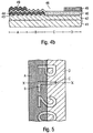
- Fig. 5 shows a security element according to the invention in plan view of the first layer structure.
- Possible layer structures of the security element are in the Fig. 2a to 4b shown.
- the in the Fig. 2a to Fig. 4b shown cross sections arise, for example, in a section along the line XX in Fig. 5 , In area A, a diffractive image with a color shift effect can be seen. In this area are translucent areas of the first layer structure and opaque areas of the second layer structure on top of each other.
- area B there is no reflector layer or no dark layer in the second layer structure, so that no color-shift effect is visible.
- the viewer therefore recognizes a translucent, diffraction-optical image.
- the diffractive-optical image can hardly be discernible due to its almost transparent properties or can be more pronounced for more reflective properties.
- the reflection may easily be e.g. be set over the layer thickness of the translucent metallization 24, 34, 44.
- region C there is no reflection layer or dark layer in the second layer structure.
- the first layer structure is transparent here, so that the viewer perceives a transparent window.
- the recesses in the reflective layer or the dark layer over their entire extent, d. h in the areas B and C, so well in the overlapping area with the translucent subregions of the first layer structure well visible in transmitted light.
- a dark or reflective layer visible.
- the layer structures are designed such that the diffraction structures of the first layer structure are imaged in the second layer structure, in particular in the reflector layer, a diffraction-optical image is visible in these areas.
- the recesses of the reflector layer or of the dark layer appear transparent in the region C and as translucent regions with a diffraction-optical image in the region B.
- the degree of translucency in turn determines the degree of visibility of the diffraction-optical image. The optically thinner the translucent layer is made, the more the diffractive image recedes compared to the transparent regions C.
- the lettering "PL20" four optically different appearing areas A, B, C, D, which can be achieved only by a precise and expensive production.
Landscapes
- Engineering & Computer Science (AREA)
- Manufacturing & Machinery (AREA)
- Physics & Mathematics (AREA)
- General Physics & Mathematics (AREA)
- Computer Security & Cryptography (AREA)
- Business, Economics & Management (AREA)
- Accounting & Taxation (AREA)
- Finance (AREA)
- Chemical & Material Sciences (AREA)
- Chemical Kinetics & Catalysis (AREA)
- General Chemical & Material Sciences (AREA)
- Health & Medical Sciences (AREA)
- Electromagnetism (AREA)
- General Health & Medical Sciences (AREA)
- Optics & Photonics (AREA)
- Toxicology (AREA)
- Credit Cards Or The Like (AREA)
- Burglar Alarm Systems (AREA)
- Laminated Bodies (AREA)
Description
Die Erfindung betrifft ein mehrschichtiges Sicherheitselement, ein Sicherheitspapier und ein Wertdokument mit einem solchen Sicherheitselement. Die Erfindung betrifft auch ein Verfahren zur Herstellung derartiger Sicherheitselemente und zur Herstellung von Sicherheitspapier.The invention relates to a multilayer security element, a security paper and a value document with such a security element. The invention also relates to a method for producing such security elements and for producing security paper.
Aus der Druckschrift
Die
Ein allgemeines Problem bei der Herstellung von Sicherheitselementen besteht darin, dass Standard-Hologramme mit einer Aluminium-Reflexionsschicht zunehmend freier verfügbar werden. Der Sicherheitsstandard derartiger Standard-Hologramme und der damit ausgestatteten Wertdokumente verringert sich daher zunehmend.A common problem in producing security features is that standard holograms with an aluminum reflective layer become increasingly more available. The safety standard of such standard holograms and the value documents equipped therewith is therefore increasingly reduced.
Ausgehend davon liegt der Erfindung die Aufgabe zugrunde, ein Sicherheitselement anzugeben, das gegenüber dem Stand der Technik eine erhöhte Fälschungssicherheit aufweist.Proceeding from this, the object of the invention is to specify a security element which has an increased security against counterfeiting compared with the prior art.
Diese Aufgabe wird durch das mehrschichtige Sicherheitselement mit den Merkmalen des Hauptanspruchs gelöst. Ein Sicherheitspapier für die Herstellung von Sicherheitsdokumenten und ein Wertdokument mit einem solchen Sicherheitselement sowie Herstellungsverfahren für ein solches Sicherheitselement und ein solches Wertdokument sind Gegenstand der nebenge-ordneten Ansprüche. Weiterbildungen der Erfindung sind Gegenstand der Unteransprüche.This object is achieved by the multilayer security element with the features of the main claim. A security paper for the production of security documents and a value document with such a security element as well as a production method for such a security element and such a value document are the subject matter of the subordinate claims. Further developments of the invention are the subject of the dependent claims.
Das erfindungsgemäße Sicherheitselement umfasst einen ersten transparenten Schichtaufbau mit ersten transluzenten Teilbereichen und einen zweiten opaken, Farbkippeffekt aufweisenden Schichtaufbau mit zweiten transparenten Teilbereichen. Der erste und zweite Schichtaufbau sind so übereinander angeordnet, dass die ersten transluzenten Teilbereiche des ersten Schichtaufbaus und die zweiten transparenten Teilbereiche des zweiten Schichtaufbaus teilweise überlappen.The security element according to the invention comprises a first transparent layer structure with first translucent subregions and a second opaque, color-shift effect layer structure with second transparent subareas. The first and second layer structure are arranged one above the other such that the first translucent subregions of the first layer structure and the second transparent subregions of the second layer structure partially overlap.
Unter "transluzent" bzw. "Transluzenz" ist im Sinne der Erfindung eine Lichtdurchlässigkeit von unter 90 %, vorzugsweise zwischen 80 % und 20 % zu verstehen.For the purposes of the invention, "translucent" or "translucency" means a light transmittance of less than 90%, preferably between 80% and 20%.
Unter "transparent" bzw. "Transparenz" ist im Sinne der Erfindung eine Lichtdurchlässigkeit von 90 % und mehr, vorzugsweise von 95 % und mehr zu verstehen.For the purposes of the invention, "transparent" or "transparency" is understood to mean a light transmittance of 90% and more, preferably 95% or more.
Unter "opak" bzw. "Opazität" ist im Sinne der Erfindung eine Lichtdurchlässigkeit von unter 10 %, vorzugsweise von 0 % zu verstehen.For the purposes of the invention, "opaque" or "opacity" means a light transmission of less than 10%, preferably 0%.
Unter "Licht" wird Licht aus dem sichtbaren Bereich des Wellenlängenspektrums (VIS) verstanden.By "light" is meant light from the visible range of the wavelength spectrum (VIS).
Im ersten Schichtaufbau sind die ersten Teilbereichen mit einer transluzenten Metallisierung versehen. Bei der transluzenten Metallisierung kann es sich um eine gerasterte Metallschicht oder um eine vollflächige, dünne Metallschicht handeln. Ist die Metallschicht vollflächig ausgeführt, liegt deren Dicke vorzugsweise zwischen 4 und 20 nm.In the first layer structure, the first subregions are provided with a translucent metallization. The translucent metallization can be a rasterized metal layer or a full-surface, thin metal layer. If the metal layer has a full surface, its thickness is preferably between 4 and 20 nm.
Die ersten Teilbereiche weisen zusätzlich Beugungsstrukturen auf. Hierzu kann in ein Substrat oder ein mit einer Prägelackschicht beschichtetes Substrat eine geeignete Struktur eingeprägt werden. Als Beugungsstrukturen kommen Refraktionsmuster, Transmissions-, Volumen- oder Reflexionshologramme, aber auch Gitterstrukturen in Betracht.The first subregions additionally have diffraction structures. For this purpose, a suitable structure can be embossed in a substrate or a substrate coated with an embossing lacquer layer. As diffraction structures refraction patterns, transmission, volume or reflection holograms, but also grid structures are considered.
Besonders bevorzugt sind Ausführungsformen, bei denen die transluzente Metallisierung und die Beugungsstrukturen deckungsgleich vorliegen. Dies ist beispielsweise dann der Fall, wenn eine Beugungsstruktur mit der transluzenten Metallschicht bedampft wird.Embodiments in which the translucent metallization and the diffraction structures are congruent are particularly preferred. This is the case, for example, when a diffraction structure is vapor-deposited with the translucent metal layer.
Der zweite opake Schichtaufbau weist einen Farbkippeffekt auf und zweite transparente Teilbereiche.The second opaque layer structure has a color shift effect and second transparent subregions.
Unter "Farbkippeffekt" ist dabei eine betrachtungswinkelabhängige Farbänderung zu verstehen.By "color shift effect" is to be understood as a viewing angle-dependent color change.
Der Farbkippeffekt wird mittels mehrschichtigem Dünnschichtaufbau oder mittels Flüssigkristallmaterialien erzeugt.The color-shift effect is produced by means of multilayer thin-film construction or by means of liquid-crystal materials.
Der Farbkippeffekt eines mehrschichtigen Dünnschichtaufbaus beruht auf Interferenzeffekten aufgrund von Mehrfachreflexionen in den verschiedenen Teilschichten des Dünnschichtelements und ist beispielsweise in der Druckschrift
Der Dünnschichtaufbau des zweiten Schichtaufbaus enthält eine opake Reflektorschicht und weitere Schichten. Bei den weiteren Schichten handelt es sich insbesondere um eine Dielektrikumsschicht und eine Absorberschicht. Vorzugsweise liegt die Dielektrikumsschicht zwischen der Reflektorschicht und der Absorberschicht.The thin-film structure of the second layer structure contains an opaque reflector layer and further layers. The further layers are, in particular, a dielectric layer and an absorber layer. Preferably, the dielectric layer lies between the reflector layer and the absorber layer.
Die Absorberschicht ist typischerweise durch dünne Metallschichten mit einer Dicke von 4 nm bis 20 nm gebildet. Als Metalle kommen insbesondere Chrom, Eisen, Gold, Aluminium oder Titan, aber auch seltenere Metalle, wie Vanadium, Palladium oder Molybdän, infrage. Darüber hinaus können beispielsweise auch Nickel, Kobalt, Wolfram, Niob oder Verbindungen und Legierungen der genannten Metalle, wie etwa Nickel-Chrom-Eisen, verwendet werden. Weitere geeignete Materialien für die Absorberschichten sind in der Druckschrift
Für die Dielektrikumsschicht kommen insbesondere aufdampfbare und durchsichtige Materialien infrage. Geeignete Materialien mit Brechungsindex kleiner 1,7 sind beispielsweise Siliziumdioxid, Aluminiumoxid, Magnesiumfluorid oder SiOx, mit 1 < x < 2. Auch Materialien mit höherem Brechungsindex, wie etwa Zirkonoxid, Zinksulfid, Titandioxid oder Indium-Zinn-Oxid, können verwendet werden. Auch für die Dielektrikumsschichten können weitere geeignete Materialien der Druckschrift
Die Dielektrikumsschichten weisen typischerweise eine Schichtdicke von etwa 100 nm bis etwa 1000 nm, bevorzugt von etwa 200 nm bis etwa 500 nm auf.The dielectric layers typically have a layer thickness of about 100 nm to about 1000 nm, preferably from about 200 nm to about 500 nm.
Bevorzugt ist die Reflektorschicht durch eine Metallschicht gebildet. In einer bevorzugten Ausgestaltung des Sicherheitselements ist die Reflektorschicht aus einem Metall der Gruppe Aluminium, Silber, Nickel, Kupfer, Gold, Eisen oder Chrom gebildet. Die verschiedenen Farben der verwendeten Metalle erlauben dann reizvolle optische Kontraste beim Betrachten des Sicherheitselements. Besonders bevorzugt besteht die Reflektorschicht aus Aluminium. Die Metallschichtdicke wird so gewählt, dass die Schicht opak ist.Preferably, the reflector layer is formed by a metal layer. In a preferred embodiment of the security element, the reflector layer is formed from a metal of the group aluminum, silver, nickel, copper, gold, iron or chromium. The different colors of the metals used then allow attractive visual contrasts when viewing the security element. Particularly preferably, the reflector layer consists of aluminum. The metal layer thickness is chosen so that the layer is opaque.
Die Absorberschicht, die Dielektrikumsschicht und die Reflektorschicht werden bevorzugt in einem Vakuumbedampfungsverfahren auf ein Substrat aufgebracht. Das Substrat kann später einen Bestandteil des fertigen Sicherheitselements bilden. Die Schichten können auch auf einem Substrat, das lediglich als Zwischenträger dient, erzeugt werden. Der Zwischenträger wird bei Fertigstellung des Sicherheitselements oder spätestens beim Aufbringen des Sicherheitselements auf einen Gegenstand entfernt. Dient das Substrat als Zwischenträger, werden die aufzubringenden Schichten in umgekehrter Reihenfolge, in der sie im Endprodukt erscheinen sollen, auf das Substrat aufgebracht. In diesem Fall wird das Sicherheitselement mit Substrat als Transferelement bezeichnet. Als Bedampfungsverfahren kommen beispielsweise PVD-Verfahren, wie Schiffchenbedampfung, Bedampfung durch Widerstands- oder Induktionsheizung, AC- und DC-Sputterverfahren, Elektronenstrahl- oder Lichtbogenbedampfung, aber auch CVD-Verfahren, wie Sputtern in einem reaktiven Plasma, oder andere plasmaunterstützte Bedampfungsverfahren, in Betracht.The absorber layer, the dielectric layer and the reflector layer are preferably applied to a substrate in a vacuum vapor deposition process. The substrate may later form part of the finished security element. The layers can also be produced on a substrate that merely serves as an intermediate carrier. The intermediate carrier is removed upon completion of the security element or at the latest when applying the security element to an object. If the substrate serves as an intermediate carrier, the layers to be applied are applied to the substrate in the reverse order in which they are to appear in the end product. In this case, the security element with substrate is referred to as a transfer element. Suitable evaporation methods are, for example, PVD processes, such as boat evaporation, evaporation by resistance or induction heating, AC and DC sputtering processes, electron beam or arc vapor deposition, but also CVD processes, such as sputtering in a reactive plasma, or other plasma-assisted vapor deposition processes ,
Das Substrat bzw. der Zwischenträger ist bevorzugt eine transparente Folie, besonders bevorzugt eine PET-Folie.The substrate or the intermediate carrier is preferably a transparent film, particularly preferably a PET film.
Alternativ kann der Farbkippeffekt mittels geeigneter Flüssigkristallmaterialien erzeugt werden. Entsprechende Sicherheitselemente sind in der
Erfindungsgemäß weist der zweite Schichtaufbau transparente zweite Teilbereiche auf. As handelt dabei um Aussparungen. Bei Verwendung von Dünnschichtaufbauten handelt es sich um Aussparungen in der Reflektor-, vorzugsweise in der Reflektor- und Absorberschicht. Bei Verwendung von Flüssigkristallmaterial handelt es sich um Aussparungen in der dunklen Schicht.According to the invention, the second layer structure has transparent second subregions. As is about recesses. When using thin-film structures are recesses in the reflector, and preferably in the reflector and absorber layer. When using liquid crystal material, these are recesses in the dark layer.
Die Aussparungen können in beliebiger Form vorliegen, vorzugsweise in Form von Mustern, Zeichen oder Codierungen. Die Aussparungen können beispielsweise in Form alphanumerischer Zeichen oder Ziffern in Positiv- oder Negativschrift, aber auch in Form beliebiger Bilddarstellungen ausgebildet sein. Eine derartige Kennung erhöht die Fälschungssicherheit des Sicherheitselements weiter, das sich dem Betrachter ansprechend und mit auch für den Laien leicht erfassbaren optischen Wirkungen präsentiert.The recesses may be in any shape, preferably in the form of patterns, characters or codes. The recesses may be formed, for example, in the form of alphanumeric characters or numbers in positive or negative writing, but also in the form of arbitrary image representations. Such an identifier further enhances the security against forgery of the security element, which presents itself to the viewer appealing and with also for the laymen easily detectable optical effects.
Die Aussparungen können nachträglich durch Ätzung, mittels Laserabtrag oder mittels Waschverfahren, wie in der
Der erste und zweite Schichtaufbau können auf einem Substrat mit einer ersten und zweiten, einander gegenüberliegenden Substratoberflächen vorliegen. Dabei können der erste und zweite Schichtaufbau auf derselben Substratoberfläche des Substrates oder alternativ auf den gegenüberliegenden Substratoberflächen vorliegen.The first and second layer structures may be on a substrate having first and second opposing substrate surfaces. In this case, the first and second layer structure can be present on the same substrate surface of the substrate or alternatively on the opposite substrate surfaces.
Die Schichtaufbauten sind zudem so angeordnet, dass der Farbkippeffekt des zweiten Schichtaufbaus bei Betrachtung des Sicherheitselementes von der Seite des ersten Schichtaufbaus her erkennbar ist.The layer structures are also arranged so that the color shift effect of the second layer structure at Contemplation of the security element can be seen from the side of the first layer structure ago.
Das Sicherheitselement ist gegenüber bekannten Sicherheitselementen somit erheblich schwerer nachstellbar. Darüber hinaus stellt die vorgeschlagene Gestaltung ein optisch ansprechendes Erkennungsmerkmal dar, das auch von einem Laien leicht erkannt und als echt bewertet werden kann.The security element is thus considerably more difficult to adjust compared to known security elements. In addition, the proposed design is a visually appealing recognition feature that can be easily recognized by a layman and evaluated as genuine.
Bei dem Substrat handelt es sich vorzugsweise um eine transparente Folie. Insbesondere eignet sich Polyethylentherephthalat (PET).The substrate is preferably a transparent film. In particular, polyethylene terephthalate (PET) is suitable.
Das erfindungsgemäße Sicherheitselement kann insbesondere überall dort sinnvoll eingesetzt werden, wo es von gegenüberliegenden Seiten her betrachtet werden kann. So kann es in oder über einer Öffnung eines Sicherheitspapiers oder eines Wertdokuments, oder in oder über einem transparenten Bereich solcher Dokumente angeordnet sein. Öffnungen und transparente Bereiche gemeinsam werden nachfolgend als Fensterbereiche eines Dokuments bezeichnet.The security element according to the invention can be used in particular wherever it can be viewed from opposite sides. Thus, it may be located in or over an opening of a security paper or a value document, or in or over a transparent area of such documents. Openings and transparent areas together are referred to below as window areas of a document.
Ebenso ist es möglich, dass das Sicherheitselement als Sicherheitsstreifen oder als Sicherheitsfaden, etwa als Fenstersicherheitsfaden eingesetzt wird. Der Schichtaufbau solcher Sicherheitsfäden wird zweckmäßig mit einer Kaschierfolie geschützt.It is also possible that the security element is used as a security strip or as a security thread, such as a window security thread. The layer structure of such security threads is expediently protected with a laminating film.
In einer anderen zweckmäßigen Ausgestaltung bildet das Sicherheitselement ein Transferelement zum Aufbringen auf ein Sicherheitspapier, Wertdokument und dergleichen. Die zu transferierenden Schichten eines solchen Transferelements sind zweckmäßig über einer Trennschicht und in umgekehrter Reihenfolge, in der sie im Endprodukt erscheinen sollen, auf das Substrat aufgebracht. Das Substrat dient als Zwischenträger und nach dem Transfer des Elements auf den zu schützenden Gegenstand wird dieses entfernt. Als Transferelemente können bandförmige Endloselemente oder Einzelelemente, sogenannte "Patches", verwendet werden.In another expedient embodiment, the security element forms a transfer element for application to a security paper, document of value and the like. The layers to be transferred of such a transfer element are expediently applied to the substrate over a release layer and in the reverse order in which they are to appear in the end product. The substrate serves as an intermediate carrier and after the transfer of the element to the object to be protected this is removed. Ribbon-shaped endless elements or individual elements, so-called "patches", can be used as transfer elements.
Die Erfindung umfasst auch ein Sicherheitspapier für die Herstellung von Wertdokumenten, wie Banknoten, Ausweiskarten oder dergleichen, mit einem oben beschriebenen Sicherheitselement. Das Sicherheitspapier kann wenigstens einen durchgehenden Fensterbereich enthalten, der mit dem Sicherheitselement bedeckt ist, so dass im Fensterbereich das Sicherheitselement bei Betrachtung von gegenüberliegenden Seiten her erkennbar ist.The invention also includes a security paper for the production of value documents, such as banknotes, identity cards or the like, with a security element described above. The security paper may include at least one continuous window area covered with the security element so that in the window area the security element is recognizable when viewed from opposite sides.
Die Erfindung enthält weiter ein Wertdokument, wie eine Banknote, eine Ausweiskarte oder dergleichen, das mit einem oben beschriebenen Sicherheitselement versehen ist. Das Wertdokument kann wenigstens einen durchgehenden Fensterbereich enthalten, der mit dem Sicherheitselement bedeckt ist, so dass im Fensterbereich das Sicherheitselement bei Betrachtung von gegenüberliegenden Seiten her erkennbar ist.The invention further includes a value document, such as a banknote, an identification card or the like, which is provided with a security element described above. The document of value may contain at least one continuous window area which is covered with the security element, so that in the window area the security element is recognizable when viewed from opposite sides.
Das erfindungsgemäße Sicherheitselement oder ein damit versehenes Sicherheitspapier oder Wertdokument können beispielsweise zur Sicherung von Waren beliebiger Art eingesetzt werden.The security element according to the invention or a security paper or value document provided therewith can be used, for example, to secure goods of any kind.
Ein Verfahren zur Herstellung eines erfindungsgemäßen Sicherheitselements für Sicherheitspapiere, Wertdokumente und dergleichen umfasst die Verfahrensschritte:
- ein erster transparenter Schichtaufbau mit ersten transluzenten Teilbereichen und
- ein zweiter opaker, Farbkippeffekt aufweisender Schichtaufbau mit zweiten transparenten Teilbereichen werden bereitgestellt,
- der erste Schichtaufbau und der zweite Schichtaufbau werden so übereinander angeordnet, dass die ersten transluzenten Teilbereiche des ersten Schichtaufbaus und die zweiten transparenten Teilbereiche des zweiten Schichtaufbaus teilweise überlappen.
- a first transparent layer structure with first translucent sections and
- a second opaque, color-shift effect layer structure with second transparent subregions is provided,
- the first layer structure and the second layer structure are arranged one above the other such that the first translucent subregions of the first layer structure and the second transparent subregions of the second layer structure partially overlap.
In einer erfindungsgemäßen Ausführungsform werden der erste und zweite Schichtaufbau auf gegenüberliegende Substratoberflächen aufgebracht. Dabei wird ein Substrat mit einer ersten und einer zweiten, einander gegenüberliegenden Substratoberflächen bereitgestellt. In das Substrat werden auf der ersten Oberfläche in den ersten Teilbereichen Beugungsstrukturen geprägt oder das Substrat wird auf der ersten Oberfläche mit einer transparenten Prägelackschicht versehen, in die in den ersten Teilbereichen Beugungsstrukturen geprägt werden. Die geprägten Teilbereiche werden mit einer transluzenten Metallschicht versehen. Auf die zweite Oberfläche wird der zweite Schichtaufbau aufgebracht.In one embodiment of the invention, the first and second layer structures are applied to opposite substrate surfaces. In this case, a substrate is provided with a first and a second, mutually opposite substrate surfaces. In the substrate, diffraction structures are embossed on the first surface in the first partial regions, or the substrate is provided on the first surface with a transparent embossing lacquer layer in which diffractive structures are embossed in the first partial regions. The embossed sections are provided with a translucent metal layer. On the second surface of the second layer structure is applied.
Auf die zweite Oberfläche des Substrates wird als zweiter Schichtaufbau eine Schicht aus Flüssigmaterial - vorzugsweise vollflächig - aufgebracht und diese anschließend bis auf die zweiten Teilbereiche mit einer dunklen, vorzugsweise schwarzen Schicht versehen wird. Vorzugsweise wird die dunkle Schicht nur bereichsweise aufgedruckt, so dass die zweiten Teilbereiche nicht bedruckt werden.On the second surface of the substrate is applied as a second layer structure, a layer of liquid material - preferably over the entire surface - and this is then provided with the exception of the second portions with a dark, preferably black layer. Preferably, the dark layer is printed only in areas, so that the second portions are not printed.
Alternativ können als zweiter Schichtaufbau auf die zweite Oberfläche des Substrates folgende Schichten in der Reihenfolge Absorber-, Dielektrikum-, Reflektorschicht aufgedampft werden.Alternatively, as second layer structure, the following layers can be vapor-deposited on the second surface of the substrate in the order of absorber, dielectric, reflector layer.
In einem weiteren erfindungsgemäßen Verfahren werden der erste und zweite Schichtaufbau auf dieselbe Substratoberfläche aufgebracht. Hierzu wird ein Substrat mit einer ersten und einer zweiten, einander gegenüberliegenden Substratoberfläche bereitgestellt, auf der ersten Oberfläche der zweite Schichtaufbau aufgebracht, auf den zweiten Schichtaufbau eine transparente Prägelackschicht aufgebracht, in die in den ersten Teilbereichen Beugungsstrukturen geprägt werden, und die geprägten Teilbereiche mit einer transluzenten Metallschicht versehen.In a further method according to the invention, the first and second layer structures are applied to the same substrate surface. For this purpose, a substrate with a first and a second, mutually opposite substrate surface is provided, on the first surface of the second layer structure is applied to the second layer structure applied a transparent embossing lacquer layer, are embossed into the diffraction structures in the first partial areas, and provided the embossed portions with a translucent metal layer.
Auf die erste Oberfläche des Substrates kann bis auf die zweiten Teilbereiche eine dunkle Schicht und darüber eine Schicht aus Flüssigmaterial - vorzugsweise vollflächig - aufgebracht werden. Alternativ können auf die erste Oberfläche des Substrates folgende Schichten in der Reihenfolge Reflektor-, Dielektrikum-, Absorberschicht aufgedampft werden.On the first surface of the substrate may be applied to the second portions of a dark layer and above a layer of liquid material - preferably over the entire surface. Alternatively, the following layers can be vapor-deposited on the first surface of the substrate in the order reflector, dielectric, absorber layer.
In einer weiteren erfindungsgemäßen Alternative wird ein Substrat mit einer ersten und einer zweiten, einander gegenüberliegenden Substratoberfläche bereitgestellt. In die erste Substratoberfläche werden in den ersten Teilbereichen entweder direkt Beugungsstrukturen geprägt oder das Substrat wird auf der ersten Oberfläche mit einer transparenten Prägelackschicht versehen, in die in den ersten Teilbereichen Beugungsstrukturen geprägt werden. Die geprägten Teilbereiche werden bevorzugt mit einer transluzenten Metallschicht versehen und darauf der zweite Schichtaufbau aufgebracht.In a further alternative according to the invention, a substrate having a first and a second, mutually opposite substrate surface is provided. Diffraction structures are either directly embossed into the first substrate surface in the first subregions, or the substrate is provided on the first surface with a transparent embossing lacquer layer in which diffractive structures are embossed in the first subregions. The embossed portions are preferably provided with a translucent metal layer and applied to the second layer structure.
Als zweiter Schichtaufbau wird zuerst eine Schicht aus Flüssigkristallmaterial und auf diese bis auf die zweiten Teilbereiche eine dunkle - vorzugsweise schwarze - Schicht aufgebracht. Alternativ können als zweiter Schichtaufbau auf die erste Oberfläche des Substrates folgende Schichten in der Reihenfolge Absorber-, Dielektrikum-, Reflektorschicht aufgedampft werden.As a second layer structure, a layer of liquid crystal material is applied first, and a dark, preferably black layer, to the second subregions. Alternatively, as a second layer structure, the following layers can be vapor-deposited on the first surface of the substrate in the order of absorber, dielectric, reflector layer.
In den Verfahrensschritten der erfindungsgemäßen Ausführungsformen, in denen die Reflektorschicht aufgebracht wird, kann zur Erzeugung der transparenten zweiten Teilbereiche die Reflektorschicht in diesen zweiten Teilbereichen nicht aufgebracht oder nachträglich entfernt werden. Insbesondere kann die Reflektorschicht mittels Ätzen, Laser oder Waschverfahren entfernt werden.In the method steps of the embodiments according to the invention, in which the reflector layer is applied, the reflector layer in these second partial areas can not be applied or subsequently removed in order to produce the transparent second partial areas. In particular, the reflector layer can be removed by means of etching, laser or washing process.
In einer weiteren Variante können ein erstes und ein zweites Substrat mit jeweils einer ersten und einer zweiten, einander gegenüberliegenden Substratoberfläche bereitgestellt werden. Auf die erste Seite des ersten Substrates wird der erste Schichtaufbau und auf die erste Seite des zweiten Substrats wird der zweite Schichtaufbau aufgebracht und das erste und zweite Substrat werden mit jeweils der zweiten Oberfläche zusammenkaschiert.In a further variant, a first and a second substrate can be provided, each having a first and a second, mutually opposite substrate surface. The first layer structure is applied to the first side of the first substrate, and the second layer structure is applied to the first side of the second substrate, and the first and second substrates are laminated together with the second surface in each case.
Das Sicherheitselement kann in weiteren Bearbeitungsschritten zur Erzeugung eines Sicherheitsfadens oder eines Transferelements entsprechend geschnitten oder gestanzt und ausgerüstet werden.The security element can be correspondingly cut or punched and equipped in further processing steps to produce a security thread or a transfer element.
Zur Herstellung eines Sicherheitspapieres wird das erfindungsgemäße Sicherheitselement in ein Papier mit einem Fensterbereich ein- oder auf das Papier aufgebracht, wobei der Fensterbereich vom Sicherheitselement überspannt wird.To produce a security paper, the security element according to the invention is applied to a paper with a window area or applied to the paper, wherein the window area is covered by the security element.
Weitere Ausführungsbeispiele sowie Vorteile der Erfindung werden nachfolgend anhand der Figuren erläutert, bei deren Darstellung auf eine maßstabs- und proportionsgetreue Wiedergabe verzichtet wurde, um die Anschaulichkeit zu erhöhen.Further exemplary embodiments and advantages of the invention are explained below with reference to the figures, in the representation of which a representation true to scale and proportion has been dispensed with in order to increase the clarity.
Es zeigen:
- Fig. 1
- eine schematische Darstellung einer Banknote mit einem erfindungsgemäßen Sicherheitselement,
- Fig. 2
- einen Querschnitt durch ein Sicherheitselement nach einem Ausführungsbeispiel der Erfindung,
- Fig. 3a, 3b und 4a, 4b
- jeweils einen Querschnitt durch ein Sicherheitselement nach einem Ausführungsbeispiel der Erfindung, und
- Fig. 5
- eine Aufsicht auf ein Sicherheitselement.
- Fig. 1
- a schematic representation of a banknote with a security element according to the invention,
- Fig. 2
- a cross section through a security element according to an embodiment of the invention,
- Fig. 3a, 3b and 4a, 4b
- in each case a cross section through a security element according to an embodiment of the invention, and
- Fig. 5
- a view of a security element.
Die Erfindung wird nachfolgend am Beispiel einer Banknote erläutert.
In den
In
Der erste und zweite Schichtaufbau können auch getrennt auf jeweils der ersten Substratoberfläche eines ersten und eines zweiten Substrats vorbereitet werden. Die mit den Schichtaufbauten ausgestatteten Substrate können dann mit den jeweils zweiten Substratoberflächen zusammenkaschiert werden (nicht gezeigt).The first and second layer structures may also be separately prepared on each of the first substrate surfaces of first and second substrates. The substrates provided with the layer structures can then be laminated together with the respective second substrate surfaces (not shown).
In
In
Die Ausführungsformen der
Im Bereich B liegt keine Reflektorschicht bzw. keine dunkle Schicht im zweiten Schichtaufbau vor, so dass kein Farbkippeffekt sichtbar ist. Im Bereich B erkennt der Betrachter also ein transluzentes, beugungsoptischen Bild. Je nach Ausgestaltung der transluzenten Eigenschaften des beugungsoptischen Bildes kann das beugungsoptische Bild aufgrund seiner fast transparenten Eigenschaften kaum erkennbar sein oder bei stärker reflektierenden Eigenschaften deutlicher hervortreten. Die Reflexion kann dabei leicht z.B. über die Schichtdicke der transluzenten Metallisierung 24, 34, 44 eingestellt werden.In area B there is no reflector layer or no dark layer in the second layer structure, so that no color-shift effect is visible. In the area B, the viewer therefore recognizes a translucent, diffraction-optical image. Depending on the configuration of the translucent properties of the diffraction-optical image, the diffractive-optical image can hardly be discernible due to its almost transparent properties or can be more pronounced for more reflective properties. The reflection may easily be e.g. be set over the layer thickness of the
Auch im Bereich C liegt keine Reflexionsschicht bzw. dunkle Schicht im zweiten Schichtaufbau vor. Der erste Schichtaufbau ist hier transparent, so dass der Betrachter ein transparentes Fenster wahrnimmt.Also in region C there is no reflection layer or dark layer in the second layer structure. The first layer structure is transparent here, so that the viewer perceives a transparent window.
Bevorzugt sind die Aussparungen in der Reflexionsschicht bzw. der dunklen Schicht über ihre gesamte Ausdehnung, d. h in den Bereichen B und C, also auch im Überlappungsbereich mit den transluzenten Teilbereichen des ersten Schichtaufbaus gut im Durchlicht erkennbar.Preferably, the recesses in the reflective layer or the dark layer over their entire extent, d. h in the areas B and C, so well in the overlapping area with the translucent subregions of the first layer structure well visible in transmitted light.
Im Bereich D liegen transparente Bereiche des ersten Schichtaufbaus und opake Bereiche des zweiten Schichtaufbaus übereinander und der Betrachter erkennt einen reinen Farbkippeffekt.In area D, transparent areas of the first layer structure and opaque areas of the second layer structure are superimposed and the viewer recognizes a pure color-shift effect.
Bei Betrachtung des Sicherheitselements von der Seite des zweiten Schichtaufbaus her ist in den Bereichen A und D (
Bei geschickter Anordnung der einzelnen Teilbereiche in den Schichtaufbauten können die verschiedensten Informationen und vielfältige Variationen davon in komplexer Form dargestellt werden. Im vorliegenden Fall weist der Schriftzug "PL20" vier optisch unterschiedlich erscheinende Bereiche A, B, C, D auf, die nur durch eine exakte und aufwendige Herstellung erzielt werden können.With skillful arrangement of the individual subregions in the layer structures, the most varied information and various variations thereof can be displayed in complex form. In the present case, the lettering "PL20" four optically different appearing areas A, B, C, D, which can be achieved only by a precise and expensive production.
Claims (15)
- A multilayer security element comprising- a first, transparent layer structure having first, translucent sub-regions, the first sub-regions exhibiting diffraction patterns (22, 33, 43) and a translucent metallization (24, 34, 44), the translucent metallization being present on the diffraction patterns (23, 33, 43), and- a second, opaque layer structure exhibiting a color-shift effect and having second, transparent sub-regions,- wherein the second layer structure is either a thin-film structure that comprises an opaque reflector layer (27, 37, 47) and further layers and wherein the second sub-regions are gaps (28, 38, 48) in the reflector layer (27, 37, 47), or comprises a layer composed of liquid crystal material (20, 30, 40) and a dark layer (29, 39, 49) and wherein the second sub-regions are gaps (28, 38, 48) in the dark layer (29, 39, 49),- wherein the first layer structure and the second layer structure are stacked on top of one another such that the first, translucent sub-regions of the first layer structure and the second, transparent sub-regions of the second layer structure partially overlap, and- wherein the further layers of the thin-film structure lie between the opaque reflector layer (27, 37, 47) and the first layer structure, or wherein the layer composed of liquid crystal material (20, 30, 40) lies between the dark layer (29, 39, 49) and the first layer structure.
- The security element according to claim 1, characterized in that the metallization is a contiguous or a screened metal layer.
- The security element according to claim 1 or 2, characterized in that the diffraction patterns are introduced into an embossing lacquer layer.
- The security element according to at least one of claims 1 to 3, characterized in that the second layer structure is a thin-film structure that comprises an opaque reflector layer and that the reflector layer consists of aluminum.
- The security element according to at least one of claims 1 to 4, characterized in that the second layer structure is a thin-film structure that comprises an opaque reflector layer and further layers and that the further layers comprise a dielectric layer and an absorber layer.
- The security element according to claim 5, characterized in that the second sub-regions are gaps in the reflector and absorber layer.
- The security element according to at least one of claims 1 to 3, characterized in that the second layer structure comprises a contiguous layer composed of liquid crystal material.
- The security element according to at least one of claims 1 to 7, characterized in that the first and second layer structure are present on a substrate having a first and a second substrate surface opposing each other.
- The security element according to claim 8, characterized in that the first and second layer structure are present on the opposing substrate surfaces of the substrate.
- A security paper having a window region and, introduced into the paper or applied to the paper, a security element according to at least one of claims 1 to 9, characterized in that the security element spans the window region (12).
- A value document comprising a security paper according to claim 10.
- A method for manufacturing a security element according to one of claims 1 to 7, in which- a first, transparent layer structure having first, translucent sub-regions and- a second, opaque layer structure exhibiting a color-shift effect and having second, transparent sub-regions are provided, and- the first layer structure and the second layer structure are stacked on top of one another such that the first, translucent sub-regions of the first layer structure and the second, transparent sub-regions of the second layer structure partially overlap,
wheretoa) a substrate having a first and a second substrate surface opposing each other is provided,b) diffraction patterns (23, 33, 43) are embossed in the substrate, in the first sub-regions on the first surface or
the substrate is provided, on the first surface, with a transparent embossing lacquer layer in which diffraction patterns (23, 33, 43) are embossed in the first sub-regions,c) the embossed sub-regions are provided with a translucent metal layer (24, 34, 44), andd) the second layer structure is applied to the second surface, whereto eitherd1) a layer composed of liquid crystal material (20, 30, 40) is applied to the second surface of the substrate, and thereafter, this layer, except for the second sub-regions, is provided with a dark layer (29, 39, 49), ord2) the following layers are vapor deposited on the second surface of the substrate in the sequence absorber layer (25, 35, 45), dielectric layer (26, 36, 46), reflector layer (27, 37, 47), and the reflector layer (27, 37, 47) is not applied in the second sub-regions, or is subsequently removed. - A method for manufacturing a security element according to one of claims 1 to 9, in which- a first, transparent layer structure having first, translucent sub-regions and- a second, opaque layer structure exhibiting a color-shift effect and having second, transparent sub-regions are provided, and- the first layer structure and the second layer structure are stacked on top of one another such that the first, translucent sub-regions of the first layer structure and the second, transparent sub-regions of the second layer structure partially overlap,
wheretoa) a substrate having a first and a second substrate surface opposing each other is provided,b) the second layer structure is applied to the first surface, whereto eitherb1) a dark layer (29, 39, 49) is applied to the first surface of the substrate except for the second sub-regions, and a layer composed of liquid crystal material (20, 30, 40) is applied over that, orb2) the following layers are vapor deposited on the first surface of the substrate in the sequence reflector layer (27, 37, 47), dielectric layer (26, 36, 46), absorber layer (25, 35, 45), and the reflector layer (27, 37, 47) is not applied in the second sub-regions, or is subsequently removed,c) a transparent embossing lacquer layer in which diffraction patterns (23, 33, 43) are embossed in the first sub-regions is applied to the second layer structure andd) the embossed sub-regions are provided with a translucent metal layer (24, 34, 44). - A method for manufacturing a security element according to one of claims 1 to 7, in which- a first, transparent layer structure having first, translucent sub-regions and- a second, opaque layer structure exhibiting a color-shift effect and having second, transparent sub-regions are provided, and- the first layer structure and the second layer structure are stacked on top of one another such that the first, translucent sub-regions of the first layer structure and the second, transparent sub-regions of the second layer structure partially overlap,
wheretoa) a substrate having a first and a second substrate surface opposing each other is provided,b) diffraction patterns (23, 33, 43) are embossed in the substrate, in the first sub-regions on the first surface or
the substrate is provided, on the first surface, with a transparent embossing lacquer layer in which diffraction patterns (23, 33, 43) are embossed in the first sub-regions,c) the embossed sub-regions are provided with a translucent metal layer (24, 34, 44), andd) the second layer structure is applied thereto, whereto eitherd1) first a layer composed of liquid crystal material (20, 30, 40) is applied, and a dark layer (29, 39, 49) is applied to that except for the second sub-regions, ord2) the following layers are vapor deposited on the first surface of the substrate in the sequence absorber layer (25, 35, 45), dielectric layer (26, 36, 46), reflector layer (27, 37, 47) and the reflector layer (27, 37, 47) is not applied in the second sub-regions, or is subsequently removed. - A method for manufacturing a security paper, characterized in that the security element according to at least one of claims 1 to 9 is introduced into a paper having a window region (12) or is applied to the paper, characterized in that the window region (12) is spanned by the security element.
Applications Claiming Priority (2)
| Application Number | Priority Date | Filing Date | Title |
|---|---|---|---|
| DE102007034716A DE102007034716A1 (en) | 2007-07-23 | 2007-07-23 | security element |
| PCT/EP2008/005624 WO2009012893A2 (en) | 2007-07-23 | 2008-07-10 | Security element |
Publications (3)
| Publication Number | Publication Date |
|---|---|
| EP2173571A2 EP2173571A2 (en) | 2010-04-14 |
| EP2173571B1 EP2173571B1 (en) | 2015-01-14 |
| EP2173571B2 true EP2173571B2 (en) | 2018-12-26 |
Family
ID=40157184
Family Applications (1)
| Application Number | Title | Priority Date | Filing Date |
|---|---|---|---|
| EP08784686.1A Active EP2173571B2 (en) | 2007-07-23 | 2008-07-10 | Security element |
Country Status (6)
| Country | Link |
|---|---|
| US (1) | US8603615B2 (en) |
| EP (1) | EP2173571B2 (en) |
| CN (1) | CN101790464B (en) |
| DE (1) | DE102007034716A1 (en) |
| RU (1) | RU2479439C2 (en) |
| WO (1) | WO2009012893A2 (en) |
Families Citing this family (51)
| Publication number | Priority date | Publication date | Assignee | Title |
|---|---|---|---|---|
| DE102005061749A1 (en) | 2005-12-21 | 2007-07-05 | Giesecke & Devrient Gmbh | Optically variable security element for making valuable objects safe has an achromatic reflecting micro-structure taking the form of a mosaic made from achromatic reflecting mosaic elements |
| GB2437939B (en) * | 2006-05-08 | 2008-03-26 | Rue De Int Ltd | Improvements in security substrates |
| DE102006058513A1 (en) | 2006-12-12 | 2008-06-19 | Giesecke & Devrient Gmbh | Drainage screen and process for its production |
| DE102007029203A1 (en) | 2007-06-25 | 2009-01-08 | Giesecke & Devrient Gmbh | security element |
| DE102007029204A1 (en) * | 2007-06-25 | 2009-01-08 | Giesecke & Devrient Gmbh | security element |
| DE102007039591A1 (en) | 2007-08-22 | 2009-02-26 | Giesecke & Devrient Gmbh | grid image |
| DE102007061827A1 (en) * | 2007-12-20 | 2009-06-25 | Giesecke & Devrient Gmbh | Security element and method for its production |
| DE102007061828A1 (en) * | 2007-12-20 | 2009-06-25 | Giesecke & Devrient Gmbh | Security element and method for its production |
| DE102007062089A1 (en) | 2007-12-21 | 2009-07-02 | Giesecke & Devrient Gmbh | Method for creating a microstructure |
| DE102007061979A1 (en) | 2007-12-21 | 2009-06-25 | Giesecke & Devrient Gmbh | security element |
| DE102008008685A1 (en) * | 2008-02-12 | 2009-08-13 | Giesecke & Devrient Gmbh | Security element and method for its production |
| DE102008009296A1 (en) * | 2008-02-15 | 2009-08-20 | Giesecke & Devrient Gmbh | Security element and method for its production |
| DE102008013167A1 (en) | 2008-03-07 | 2009-09-10 | Giesecke & Devrient Gmbh | Security element and method for its production |
| DE102008016795A1 (en) | 2008-04-02 | 2009-10-08 | Giesecke & Devrient Gmbh | Method for producing a micro-optical moiré magnification arrangement |
| DE102008028187A1 (en) | 2008-06-12 | 2009-12-17 | Giesecke & Devrient Gmbh | Security element with optically variable element. |
| DE102008027952A1 (en) * | 2008-06-12 | 2009-12-17 | Giesecke & Devrient Gmbh | Security element with screened layer of raster elements |
| DE102008029638A1 (en) | 2008-06-23 | 2009-12-24 | Giesecke & Devrient Gmbh | security element |
| DE102008031325A1 (en) | 2008-07-02 | 2010-01-07 | Giesecke & Devrient Gmbh | Security element and method for its production |
| DE102008032224A1 (en) * | 2008-07-09 | 2010-01-14 | Giesecke & Devrient Gmbh | security element |
| DE102008046511A1 (en) | 2008-09-10 | 2010-03-11 | Giesecke & Devrient Gmbh | representation arrangement |
| DE102009035413A1 (en) | 2009-07-31 | 2011-02-03 | Giesecke & Devrient Gmbh | Identification document with a personalized visual identification and method for its production |
| DE102009041583A1 (en) | 2009-09-15 | 2011-03-17 | Giesecke & Devrient Gmbh | Thin-film element with interference layer structure |
| DE102009042022A1 (en) | 2009-09-21 | 2011-03-24 | Giesecke & Devrient Gmbh | Elongated security element with machine-readable magnetic areas |
| EP2322356A1 (en) * | 2009-11-13 | 2011-05-18 | Gemalto SA | Identification document and a method of producing |
| CH701875A3 (en) * | 2011-01-18 | 2011-11-30 | Trueb Ag | Method for producing a multilayer data carrier and data carrier produced by this method. |
| JP5929013B2 (en) * | 2011-05-25 | 2016-06-01 | 凸版印刷株式会社 | Colored anti-counterfeit structure and colored anti-counterfeit medium |
| CN102644216B (en) * | 2012-03-29 | 2015-02-25 | 西安印钞有限公司 | Safety line and anti-counterfeiting paper thereof |
| US9279927B2 (en) * | 2013-02-15 | 2016-03-08 | Opsec Security Group, Inc. | Security device having optically variable device portion and method of making the same |
| GB201316348D0 (en) * | 2013-09-13 | 2013-10-30 | Andrews & Wykeham Ltd | Security laminate/foil |
| GB201400910D0 (en) | 2014-01-20 | 2014-03-05 | Rue De Int Ltd | Security elements and methods of their manufacture |
| USD780463S1 (en) * | 2014-03-31 | 2017-03-07 | Giesecke & Devrient Gmbh | Sheet document with security element |
| USD769000S1 (en) * | 2014-03-31 | 2016-10-18 | Giesecke & Devrient Gmbh | Sheet document with security element |
| US10086638B2 (en) | 2014-10-07 | 2018-10-02 | Morphotrust Usa, Llc | System and method for laser writing |
| FR3033735B1 (en) * | 2015-03-16 | 2022-03-04 | Arjowiggins Security | SECURITY ELEMENT AND SECURE DOCUMENT |
| DE102015003665A1 (en) * | 2015-03-20 | 2016-09-22 | Giesecke & Devrient Gmbh | security element |
| DE102015010811A1 (en) * | 2015-08-21 | 2017-02-23 | Veridos Gmbh | Multi-layered data carrier with a flat see-through window |
| JP6187611B2 (en) * | 2016-01-18 | 2017-08-30 | 凸版印刷株式会社 | Colored anti-counterfeit structure and colored anti-counterfeit medium |
| GB2555491B (en) | 2016-11-01 | 2019-03-27 | De La Rue Int Ltd | Security devices and methods of manufacture thereof |
| GB2563187B (en) | 2017-02-03 | 2020-07-22 | De La Rue Int Ltd | Method of forming a security sheet substrate |
| GB2562699B (en) | 2017-02-03 | 2020-07-22 | De La Rue Int Ltd | Method of forming a security device |
| WO2018169441A1 (en) * | 2017-03-11 | 2018-09-20 | Andrey Karasev | Security ovd |
| DE102018103236A1 (en) * | 2018-02-14 | 2019-08-14 | Leonhard Kurz Stiftung & Co. Kg | Security element and method for producing a security element |
| DE102018005447A1 (en) * | 2018-07-09 | 2020-01-09 | Giesecke+Devrient Currency Technology Gmbh | Optically variable security element with reflective surface area |
| DE102018005454A1 (en) * | 2018-07-09 | 2020-01-09 | Giesecke+Devrient Currency Technology Gmbh | Optically variable security element with reflective surface area |
| WO2020217254A1 (en) | 2019-04-20 | 2020-10-29 | Shilpan Patel | Robust colour shift security film with wide spectrum complex spectral values and security thread made therefrom |
| DE102019003945A1 (en) * | 2019-06-06 | 2020-12-10 | Giesecke+Devrient Currency Technology Gmbh | Optically variable security element with multicolored reflective surface area |
| CN112572018B (en) * | 2019-09-29 | 2022-06-14 | 中钞特种防伪科技有限公司 | Multilayer optical anti-counterfeiting element and manufacturing method thereof |
| JP7181908B2 (en) * | 2020-04-15 | 2022-12-01 | 株式会社バンダイ | model parts |
| WO2022002366A1 (en) * | 2020-06-30 | 2022-01-06 | Fase S.R.L. | Multifunction security element |
| CN111923621B (en) * | 2020-07-23 | 2022-04-19 | 深圳市嘉大嘉智能包装有限公司 | Enamel color manufacturing process |
| DE102020006902A1 (en) | 2020-11-10 | 2022-05-12 | Giesecke+Devrient Currency Technology Gmbh | Optically variable security element and method for producing an optically variable security element |
Citations (12)
| Publication number | Priority date | Publication date | Assignee | Title |
|---|---|---|---|---|
| EP0201323A2 (en) † | 1985-05-07 | 1986-11-12 | Dai Nippon Insatsu Kabushiki Kaisha | Article incorporating a transparent hologramm |
| EP0328086A2 (en) † | 1988-02-12 | 1989-08-16 | American Bank Note Holographics, Inc. | Articles incorporating non-continuous holographs and methods of making them |
| WO1995010420A1 (en) † | 1993-10-13 | 1995-04-20 | Leonhard Kurz Gmbh & Co. | Security document with window |
| WO2001053113A1 (en) † | 2000-01-21 | 2001-07-26 | Flex Products, Inc. | Optically variable security devices |
| WO2002000445A1 (en) † | 2000-06-28 | 2002-01-03 | De La Rue International Limited | Optically variable security device |
| WO2003054297A2 (en) † | 2001-12-21 | 2003-07-03 | Giesecke & Devrient Gmbh | Security paper and method and device for producing the same |
| WO2003091042A2 (en) † | 2002-04-26 | 2003-11-06 | Giesecke & Devrient Gmbh | Security element comprising metallic layers |
| WO2003095227A1 (en) † | 2002-05-14 | 2003-11-20 | Leonhard Kurz Gmbh & Co. Kg | Optically variable element comprising a partially transparent element |
| WO2003095228A1 (en) † | 2002-05-14 | 2003-11-20 | Leonhard Kurz Gmbh & Co. Kg | Optically variable element comprising a sequence of thin-film layers |
| WO2004095090A1 (en) † | 2003-04-17 | 2004-11-04 | Leonhard Kurz Gmbh & Co. Kg | Film and optical anti-counterfeiting element |
| WO2005026848A2 (en) † | 2003-09-18 | 2005-03-24 | Jds Uniphase Corporation | Patterned reflective optical micro-structures |
| WO2006002756A2 (en) † | 2004-07-05 | 2006-01-12 | Giesecke & Devrient Gmbh | Security element with a color shift tilt effect |
Family Cites Families (43)
| Publication number | Priority date | Publication date | Assignee | Title |
|---|---|---|---|---|
| US5278590A (en) | 1989-04-26 | 1994-01-11 | Flex Products, Inc. | Transparent optically variable device |
| DE3942663A1 (en) | 1989-12-22 | 1991-06-27 | Gao Ges Automation Org | DATA CARRIER WITH A LIQUID CRYSTAL SECURITY ELEMENT |
| DE19739193B4 (en) | 1997-09-08 | 2006-08-03 | Giesecke & Devrient Gmbh | Method for producing security films for securities |
| US6761959B1 (en) * | 1999-07-08 | 2004-07-13 | Flex Products, Inc. | Diffractive surfaces with color shifting backgrounds |
| DE10202035B4 (en) * | 2002-01-18 | 2018-10-18 | Giesecke+Devrient Currency Technology Gmbh | Security element with color shift effect and magnetic properties, article with such a security element and method for producing the security element and the article. |
| GB0201767D0 (en) * | 2002-01-25 | 2002-03-13 | Rue De Int Ltd | Improvements in methods of manufacturing substrates |
| DE10206357A1 (en) * | 2002-02-14 | 2003-08-28 | Giesecke & Devrient Gmbh | Security element and security document with such a security element |
| DE10319232A1 (en) | 2003-04-28 | 2004-11-18 | Giesecke & Devrient Gmbh | Flat security element and manufacturing method for the same |
| AT501356A1 (en) * | 2003-06-18 | 2006-08-15 | Hueck Folien Gmbh | SAFETY ELEMENTS AND SAFETY FEATURES WITH COLOR EFFECTS |
| DE10351129B4 (en) * | 2003-11-03 | 2008-12-24 | Ovd Kinegram Ag | Diffractive security element with a halftone image |
| EP2749430B1 (en) * | 2004-04-14 | 2016-02-17 | Dai Nippon Printing Co., Ltd. | Authentication medium |
| DE102004039355A1 (en) * | 2004-08-12 | 2006-02-23 | Giesecke & Devrient Gmbh | Security element and method for its production |
| US20070211238A1 (en) | 2004-04-30 | 2007-09-13 | Giesecke & Devrient Gmbh | Security Element and Methods for the Production Thereof |
| DE102004021247A1 (en) | 2004-04-30 | 2005-11-24 | Giesecke & Devrient Gmbh | Security element and method for its production |
| DE102004021246A1 (en) | 2004-04-30 | 2005-11-24 | Giesecke & Devrient Gmbh | Security element and method for its production |
| US7808605B2 (en) | 2004-04-30 | 2010-10-05 | Giesecke & Devrient Gmbh | Sheeting and methods for the production thereof |
| BRPI0510502B1 (en) * | 2004-04-30 | 2015-07-21 | Syngenta Participations Ag | Process for the production of cyclic diketones, as well as their intermediates |
| DE102004022080A1 (en) | 2004-05-05 | 2005-11-24 | Giesecke & Devrient Gmbh | Value document with visually recognizable markings |
| DE102004022079A1 (en) * | 2004-05-05 | 2005-11-24 | Giesecke & Devrient Gmbh | Value document with serial number |
| DE102004035979A1 (en) | 2004-07-14 | 2006-02-02 | Giesecke & Devrient Gmbh | Security element and method for its production |
| DE102004038542A1 (en) | 2004-08-06 | 2006-02-23 | Giesecke & Devrient Gmbh | Data carrier with security element and method for its production |
| ES2428360T5 (en) | 2004-08-12 | 2019-04-16 | Giesecke & Devrient Currency Technology Gmbh | Security element with support |
| DE102004049118A1 (en) | 2004-10-07 | 2006-04-13 | Giesecke & Devrient Gmbh | Security element and method for its production |
| DE102004056553B4 (en) | 2004-11-23 | 2013-03-14 | Giesecke & Devrient Gmbh | Security arrangement for security documents and method for producing the security documents |
| DE102004063217A1 (en) | 2004-12-29 | 2006-07-13 | Giesecke & Devrient Gmbh | Security feature for value documents |
| DE102005028162A1 (en) | 2005-02-18 | 2006-12-28 | Giesecke & Devrient Gmbh | Security element for protecting valuable objects, e.g. documents, includes focusing components for enlarging views of microscopic structures as one of two authenication features |
| DE102005045566A1 (en) | 2005-03-23 | 2006-09-28 | Giesecke & Devrient Gmbh | Multi-layer security paper |
| DE102005022018A1 (en) | 2005-05-12 | 2006-11-16 | Giesecke & Devrient Gmbh | Security paper and process for its production |
| DE102005025095A1 (en) | 2005-06-01 | 2006-12-07 | Giesecke & Devrient Gmbh | Data carrier and method for its production |
| DE102005032815A1 (en) | 2005-07-12 | 2007-01-18 | Giesecke & Devrient Gmbh | Method for producing a security paper, paper screen and forming element for paper screen |
| DE102005032997A1 (en) | 2005-07-14 | 2007-01-18 | Giesecke & Devrient Gmbh | Lattice image and method for its production |
| DE102005061749A1 (en) | 2005-12-21 | 2007-07-05 | Giesecke & Devrient Gmbh | Optically variable security element for making valuable objects safe has an achromatic reflecting micro-structure taking the form of a mosaic made from achromatic reflecting mosaic elements |
| DE102005062132A1 (en) | 2005-12-23 | 2007-07-05 | Giesecke & Devrient Gmbh | Security unit e.g. seal, for e.g. valuable document, has motive image with planar periodic arrangement of micro motive units, and periodic arrangement of lens for moire magnified observation of motive units |
| DE102006015023A1 (en) | 2006-03-31 | 2007-10-04 | Giesecke & Devrient Gmbh | Security element for security papers, value documents, has relief structure, which is formed on basis of cholesteric, liquid crystalline polymer material and top layer contains reflecting or high-refracting layer |
| GB2438383B (en) | 2006-05-26 | 2008-10-08 | Rue De Int Ltd | Improvements in substrates |
| DE102006029852A1 (en) | 2006-06-27 | 2008-01-03 | Giesecke & Devrient Gmbh | Method of applying a microstructure, mold and microstructured article |
| DE102006029850A1 (en) | 2006-06-27 | 2008-01-03 | Giesecke & Devrient Gmbh | security element |
| DE102006039305A1 (en) | 2006-07-21 | 2008-01-24 | Giesecke & Devrient Gmbh | Security thread with optically variable security feature |
| DE102006050047A1 (en) | 2006-10-24 | 2008-04-30 | Giesecke & Devrient Gmbh | Transparent security element for security papers, data carrier, particularly valuable documents such as bank note, identification card and for falsification of goods, has transparent substrate and marking layer applied on substrate |
| DE102006055680A1 (en) | 2006-11-23 | 2008-05-29 | Giesecke & Devrient Gmbh | Security element with metallization |
| DE102006058513A1 (en) | 2006-12-12 | 2008-06-19 | Giesecke & Devrient Gmbh | Drainage screen and process for its production |
| DE102007029204A1 (en) | 2007-06-25 | 2009-01-08 | Giesecke & Devrient Gmbh | security element |
| DE102007029203A1 (en) | 2007-06-25 | 2009-01-08 | Giesecke & Devrient Gmbh | security element |
-
2007
- 2007-07-23 DE DE102007034716A patent/DE102007034716A1/en not_active Withdrawn
-
2008
- 2008-07-10 WO PCT/EP2008/005624 patent/WO2009012893A2/en not_active Ceased
- 2008-07-10 US US12/669,838 patent/US8603615B2/en not_active Expired - Fee Related
- 2008-07-10 CN CN200880025683.9A patent/CN101790464B/en active Active
- 2008-07-10 EP EP08784686.1A patent/EP2173571B2/en active Active
- 2008-07-10 RU RU2010105631/12A patent/RU2479439C2/en not_active IP Right Cessation
Patent Citations (12)
| Publication number | Priority date | Publication date | Assignee | Title |
|---|---|---|---|---|
| EP0201323A2 (en) † | 1985-05-07 | 1986-11-12 | Dai Nippon Insatsu Kabushiki Kaisha | Article incorporating a transparent hologramm |
| EP0328086A2 (en) † | 1988-02-12 | 1989-08-16 | American Bank Note Holographics, Inc. | Articles incorporating non-continuous holographs and methods of making them |
| WO1995010420A1 (en) † | 1993-10-13 | 1995-04-20 | Leonhard Kurz Gmbh & Co. | Security document with window |
| WO2001053113A1 (en) † | 2000-01-21 | 2001-07-26 | Flex Products, Inc. | Optically variable security devices |
| WO2002000445A1 (en) † | 2000-06-28 | 2002-01-03 | De La Rue International Limited | Optically variable security device |
| WO2003054297A2 (en) † | 2001-12-21 | 2003-07-03 | Giesecke & Devrient Gmbh | Security paper and method and device for producing the same |
| WO2003091042A2 (en) † | 2002-04-26 | 2003-11-06 | Giesecke & Devrient Gmbh | Security element comprising metallic layers |
| WO2003095227A1 (en) † | 2002-05-14 | 2003-11-20 | Leonhard Kurz Gmbh & Co. Kg | Optically variable element comprising a partially transparent element |
| WO2003095228A1 (en) † | 2002-05-14 | 2003-11-20 | Leonhard Kurz Gmbh & Co. Kg | Optically variable element comprising a sequence of thin-film layers |
| WO2004095090A1 (en) † | 2003-04-17 | 2004-11-04 | Leonhard Kurz Gmbh & Co. Kg | Film and optical anti-counterfeiting element |
| WO2005026848A2 (en) † | 2003-09-18 | 2005-03-24 | Jds Uniphase Corporation | Patterned reflective optical micro-structures |
| WO2006002756A2 (en) † | 2004-07-05 | 2006-01-12 | Giesecke & Devrient Gmbh | Security element with a color shift tilt effect |
Also Published As
| Publication number | Publication date |
|---|---|
| EP2173571A2 (en) | 2010-04-14 |
| DE102007034716A1 (en) | 2009-01-29 |
| WO2009012893A2 (en) | 2009-01-29 |
| WO2009012893A8 (en) | 2009-03-12 |
| WO2009012893A3 (en) | 2009-12-30 |
| CN101790464B (en) | 2016-01-20 |
| RU2010105631A (en) | 2011-08-27 |
| US20100196587A1 (en) | 2010-08-05 |
| EP2173571B1 (en) | 2015-01-14 |
| CN101790464A (en) | 2010-07-28 |
| US8603615B2 (en) | 2013-12-10 |
| RU2479439C2 (en) | 2013-04-20 |
Similar Documents
| Publication | Publication Date | Title |
|---|---|---|
| EP2173571B2 (en) | Security element | |
| EP1476315B1 (en) | Security element and security document with one such security element | |
| EP1478520B1 (en) | Security document and security element for a security document | |
| EP1458575B2 (en) | Security element for security papers and valuable documents | |
| EP1620602B1 (en) | Planar security element and method for the production thereof | |
| EP3337674B1 (en) | Valuable document | |
| DE102004032565A1 (en) | Security element with color shift effect | |
| DE10202035A1 (en) | Authenticity security mark for financial instruments combines color shift with magnetic and reflective layers | |
| EP2147156B1 (en) | Security paper | |
| EP3260302A1 (en) | Optically variable security element | |
| EP3212430B1 (en) | Security element with colourshifting thin film | |
| EP4311683A1 (en) | Security element and valuable document equipped with the security element | |
| EP1547807A2 (en) | Security element having a diffraction structure and method of manufacturing said element | |
| WO2022033653A1 (en) | Elongate security element and method for producing an elongate security element | |
| EP3606766B1 (en) | Security element and method for the production thereof | |
| WO2017025175A1 (en) | Security element |
Legal Events
| Date | Code | Title | Description |
|---|---|---|---|
| PUAI | Public reference made under article 153(3) epc to a published international application that has entered the european phase |
Free format text: ORIGINAL CODE: 0009012 |
|
| AK | Designated contracting states |
Kind code of ref document: A2 Designated state(s): AT BE BG CH CY CZ DE DK EE ES FI FR GB GR HR HU IE IS IT LI LT LU LV MC MT NL NO PL PT RO SE SI SK TR |
|
| AX | Request for extension of the european patent |
Extension state: AL BA MK RS |
|
| 17P | Request for examination filed |
Effective date: 20100630 |
|
| RBV | Designated contracting states (corrected) |
Designated state(s): AT BE BG CH CY CZ DE DK EE ES FI FR GB GR HR HU IE IS IT LI LT LU LV MC MT NL NO PL PT RO SE SI SK TR |
|
| 17Q | First examination report despatched |
Effective date: 20100803 |
|
| DAX | Request for extension of the european patent (deleted) | ||
| REG | Reference to a national code |
Ref country code: DE Ref legal event code: R079 Ref document number: 502008012613 Country of ref document: DE Free format text: PREVIOUS MAIN CLASS: B44F0001120000 Ipc: B42D0025300000 |
|
| GRAP | Despatch of communication of intention to grant a patent |
Free format text: ORIGINAL CODE: EPIDOSNIGR1 |
|
| RIC1 | Information provided on ipc code assigned before grant |
Ipc: B42D 25/328 20140101ALN20140730BHEP Ipc: B42D 25/373 20140101ALN20140730BHEP Ipc: B42D 25/30 20140101AFI20140730BHEP |
|
| RIC1 | Information provided on ipc code assigned before grant |
Ipc: B42D 25/30 20140101AFI20140811BHEP Ipc: B42D 25/373 20140101ALN20140811BHEP Ipc: B42D 25/328 20140101ALN20140811BHEP |
|
| INTG | Intention to grant announced |
Effective date: 20140829 |
|
| GRAS | Grant fee paid |
Free format text: ORIGINAL CODE: EPIDOSNIGR3 |
|
| GRAA | (expected) grant |
Free format text: ORIGINAL CODE: 0009210 |
|
| AK | Designated contracting states |
Kind code of ref document: B1 Designated state(s): AT BE BG CH CY CZ DE DK EE ES FI FR GB GR HR HU IE IS IT LI LT LU LV MC MT NL NO PL PT RO SE SI SK TR |
|
| REG | Reference to a national code |
Ref country code: GB Ref legal event code: FG4D Free format text: NOT ENGLISH |
|
| REG | Reference to a national code |
Ref country code: CH Ref legal event code: EP |
|
| REG | Reference to a national code |
Ref country code: IE Ref legal event code: FG4D Free format text: LANGUAGE OF EP DOCUMENT: GERMAN |
|
| REG | Reference to a national code |
Ref country code: CH Ref legal event code: NV Representative=s name: RENTSCH PARTNER AG, CH |
|
| REG | Reference to a national code |
Ref country code: AT Ref legal event code: REF Ref document number: 706812 Country of ref document: AT Kind code of ref document: T Effective date: 20150215 |
|
| REG | Reference to a national code |
Ref country code: DE Ref legal event code: R096 Ref document number: 502008012613 Country of ref document: DE Effective date: 20150305 |
|
| REG | Reference to a national code |
Ref country code: NL Ref legal event code: VDEP Effective date: 20150114 |
|
| REG | Reference to a national code |
Ref country code: LT Ref legal event code: MG4D |
|
| REG | Reference to a national code |
Ref country code: FR Ref legal event code: PLFP Year of fee payment: 8 |
|
| PG25 | Lapsed in a contracting state [announced via postgrant information from national office to epo] |
Ref country code: SE Free format text: LAPSE BECAUSE OF FAILURE TO SUBMIT A TRANSLATION OF THE DESCRIPTION OR TO PAY THE FEE WITHIN THE PRESCRIBED TIME-LIMIT Effective date: 20150114 Ref country code: HR Free format text: LAPSE BECAUSE OF FAILURE TO SUBMIT A TRANSLATION OF THE DESCRIPTION OR TO PAY THE FEE WITHIN THE PRESCRIBED TIME-LIMIT Effective date: 20150114 Ref country code: LT Free format text: LAPSE BECAUSE OF FAILURE TO SUBMIT A TRANSLATION OF THE DESCRIPTION OR TO PAY THE FEE WITHIN THE PRESCRIBED TIME-LIMIT Effective date: 20150114 Ref country code: FI Free format text: LAPSE BECAUSE OF FAILURE TO SUBMIT A TRANSLATION OF THE DESCRIPTION OR TO PAY THE FEE WITHIN THE PRESCRIBED TIME-LIMIT Effective date: 20150114 Ref country code: ES Free format text: LAPSE BECAUSE OF FAILURE TO SUBMIT A TRANSLATION OF THE DESCRIPTION OR TO PAY THE FEE WITHIN THE PRESCRIBED TIME-LIMIT Effective date: 20150114 Ref country code: NO Free format text: LAPSE BECAUSE OF FAILURE TO SUBMIT A TRANSLATION OF THE DESCRIPTION OR TO PAY THE FEE WITHIN THE PRESCRIBED TIME-LIMIT Effective date: 20150414 Ref country code: BG Free format text: LAPSE BECAUSE OF FAILURE TO SUBMIT A TRANSLATION OF THE DESCRIPTION OR TO PAY THE FEE WITHIN THE PRESCRIBED TIME-LIMIT Effective date: 20150414 |
|
| PG25 | Lapsed in a contracting state [announced via postgrant information from national office to epo] |
Ref country code: IS Free format text: LAPSE BECAUSE OF FAILURE TO SUBMIT A TRANSLATION OF THE DESCRIPTION OR TO PAY THE FEE WITHIN THE PRESCRIBED TIME-LIMIT Effective date: 20150514 Ref country code: LV Free format text: LAPSE BECAUSE OF FAILURE TO SUBMIT A TRANSLATION OF THE DESCRIPTION OR TO PAY THE FEE WITHIN THE PRESCRIBED TIME-LIMIT Effective date: 20150114 Ref country code: GR Free format text: LAPSE BECAUSE OF FAILURE TO SUBMIT A TRANSLATION OF THE DESCRIPTION OR TO PAY THE FEE WITHIN THE PRESCRIBED TIME-LIMIT Effective date: 20150415 Ref country code: NL Free format text: LAPSE BECAUSE OF FAILURE TO SUBMIT A TRANSLATION OF THE DESCRIPTION OR TO PAY THE FEE WITHIN THE PRESCRIBED TIME-LIMIT Effective date: 20150114 Ref country code: PL Free format text: LAPSE BECAUSE OF FAILURE TO SUBMIT A TRANSLATION OF THE DESCRIPTION OR TO PAY THE FEE WITHIN THE PRESCRIBED TIME-LIMIT Effective date: 20150114 |
|
| REG | Reference to a national code |
Ref country code: DE Ref legal event code: R026 Ref document number: 502008012613 Country of ref document: DE |
|
| PLBI | Opposition filed |
Free format text: ORIGINAL CODE: 0009260 |
|
| PG25 | Lapsed in a contracting state [announced via postgrant information from national office to epo] |
Ref country code: RO Free format text: LAPSE BECAUSE OF FAILURE TO SUBMIT A TRANSLATION OF THE DESCRIPTION OR TO PAY THE FEE WITHIN THE PRESCRIBED TIME-LIMIT Effective date: 20150114 Ref country code: DK Free format text: LAPSE BECAUSE OF FAILURE TO SUBMIT A TRANSLATION OF THE DESCRIPTION OR TO PAY THE FEE WITHIN THE PRESCRIBED TIME-LIMIT Effective date: 20150114 Ref country code: EE Free format text: LAPSE BECAUSE OF FAILURE TO SUBMIT A TRANSLATION OF THE DESCRIPTION OR TO PAY THE FEE WITHIN THE PRESCRIBED TIME-LIMIT Effective date: 20150114 Ref country code: SK Free format text: LAPSE BECAUSE OF FAILURE TO SUBMIT A TRANSLATION OF THE DESCRIPTION OR TO PAY THE FEE WITHIN THE PRESCRIBED TIME-LIMIT Effective date: 20150114 Ref country code: CZ Free format text: LAPSE BECAUSE OF FAILURE TO SUBMIT A TRANSLATION OF THE DESCRIPTION OR TO PAY THE FEE WITHIN THE PRESCRIBED TIME-LIMIT Effective date: 20150114 |
|
| PLAX | Notice of opposition and request to file observation + time limit sent |
Free format text: ORIGINAL CODE: EPIDOSNOBS2 |
|
| 26 | Opposition filed |
Opponent name: LEONHARD KURZ STIFTUNG & CO. KG Effective date: 20151013 |
|
| PG25 | Lapsed in a contracting state [announced via postgrant information from national office to epo] |
Ref country code: SI Free format text: LAPSE BECAUSE OF FAILURE TO SUBMIT A TRANSLATION OF THE DESCRIPTION OR TO PAY THE FEE WITHIN THE PRESCRIBED TIME-LIMIT Effective date: 20150114 Ref country code: MC Free format text: LAPSE BECAUSE OF FAILURE TO SUBMIT A TRANSLATION OF THE DESCRIPTION OR TO PAY THE FEE WITHIN THE PRESCRIBED TIME-LIMIT Effective date: 20150114 |
|
| PLAF | Information modified related to communication of a notice of opposition and request to file observations + time limit |
Free format text: ORIGINAL CODE: EPIDOSCOBS2 |
|
| PG25 | Lapsed in a contracting state [announced via postgrant information from national office to epo] |
Ref country code: LU Free format text: LAPSE BECAUSE OF FAILURE TO SUBMIT A TRANSLATION OF THE DESCRIPTION OR TO PAY THE FEE WITHIN THE PRESCRIBED TIME-LIMIT Effective date: 20150710 |
|
| REG | Reference to a national code |
Ref country code: IE Ref legal event code: MM4A |
|
| PLBB | Reply of patent proprietor to notice(s) of opposition received |
Free format text: ORIGINAL CODE: EPIDOSNOBS3 |
|
| REG | Reference to a national code |
Ref country code: FR Ref legal event code: PLFP Year of fee payment: 9 |
|
| PG25 | Lapsed in a contracting state [announced via postgrant information from national office to epo] |
Ref country code: IE Free format text: LAPSE BECAUSE OF NON-PAYMENT OF DUE FEES Effective date: 20150710 |
|
| PG25 | Lapsed in a contracting state [announced via postgrant information from national office to epo] |
Ref country code: MT Free format text: LAPSE BECAUSE OF FAILURE TO SUBMIT A TRANSLATION OF THE DESCRIPTION OR TO PAY THE FEE WITHIN THE PRESCRIBED TIME-LIMIT Effective date: 20150114 |
|
| PG25 | Lapsed in a contracting state [announced via postgrant information from national office to epo] |
Ref country code: HU Free format text: LAPSE BECAUSE OF FAILURE TO SUBMIT A TRANSLATION OF THE DESCRIPTION OR TO PAY THE FEE WITHIN THE PRESCRIBED TIME-LIMIT; INVALID AB INITIO Effective date: 20080710 |
|
| PG25 | Lapsed in a contracting state [announced via postgrant information from national office to epo] |
Ref country code: CY Free format text: LAPSE BECAUSE OF FAILURE TO SUBMIT A TRANSLATION OF THE DESCRIPTION OR TO PAY THE FEE WITHIN THE PRESCRIBED TIME-LIMIT Effective date: 20150114 |
|
| REG | Reference to a national code |
Ref country code: FR Ref legal event code: PLFP Year of fee payment: 10 |
|
| PG25 | Lapsed in a contracting state [announced via postgrant information from national office to epo] |
Ref country code: BE Free format text: LAPSE BECAUSE OF NON-PAYMENT OF DUE FEES Effective date: 20150731 |
|
| REG | Reference to a national code |
Ref country code: DE Ref legal event code: R081 Ref document number: 502008012613 Country of ref document: DE Owner name: GIESECKE+DEVRIENT CURRENCY TECHNOLOGY GMBH, DE Free format text: FORMER OWNER: GIESECKE & DEVRIENT GMBH, 81677 MUENCHEN, DE |
|
| PG25 | Lapsed in a contracting state [announced via postgrant information from national office to epo] |
Ref country code: TR Free format text: LAPSE BECAUSE OF FAILURE TO SUBMIT A TRANSLATION OF THE DESCRIPTION OR TO PAY THE FEE WITHIN THE PRESCRIBED TIME-LIMIT Effective date: 20150114 |
|
| REG | Reference to a national code |
Ref country code: CH Ref legal event code: PCAR Free format text: NEW ADDRESS: BELLERIVESTRASSE 203 POSTFACH, 8034 ZUERICH (CH) |
|
| REG | Reference to a national code |
Ref country code: CH Ref legal event code: PUE Owner name: GIESECKE+DEVRIENT CURRENCY TECHNOLOGY GMBH, DE Free format text: FORMER OWNER: GIESECKE AND DEVRIENT GMBH, DE |
|
| REG | Reference to a national code |
Ref country code: GB Ref legal event code: 732E Free format text: REGISTERED BETWEEN 20180118 AND 20180124 |
|
| RAP2 | Party data changed (patent owner data changed or rights of a patent transferred) |
Owner name: GIESECKE+DEVRIENT CURRENCY TECHNOLOGY GMBH |
|
| RDAF | Communication despatched that patent is revoked |
Free format text: ORIGINAL CODE: EPIDOSNREV1 |
|
| STAA | Information on the status of an ep patent application or granted ep patent |
Free format text: STATUS: THE PATENT HAS BEEN GRANTED |
|
| REG | Reference to a national code |
Ref country code: AT Ref legal event code: PC Ref document number: 706812 Country of ref document: AT Kind code of ref document: T Owner name: GIESECKE+DEVRIENT CURRENCY TECHNOLOGY GMBH, DE Effective date: 20180426 |
|
| PG25 | Lapsed in a contracting state [announced via postgrant information from national office to epo] |
Ref country code: PT Free format text: LAPSE BECAUSE OF FAILURE TO SUBMIT A TRANSLATION OF THE DESCRIPTION OR TO PAY THE FEE WITHIN THE PRESCRIBED TIME-LIMIT Effective date: 20150114 |
|
| REG | Reference to a national code |
Ref country code: FR Ref legal event code: TP Owner name: GIESECKE+DEVRIENT CURRENCY TECHNOLOGY GMBH, DE Effective date: 20180530 |
|
| REG | Reference to a national code |
Ref country code: FR Ref legal event code: PLFP Year of fee payment: 11 |
|
| RDAE | Information deleted related to despatch of communication that patent is revoked |
Free format text: ORIGINAL CODE: EPIDOSDREV1 |
|
| PUAH | Patent maintained in amended form |
Free format text: ORIGINAL CODE: 0009272 |
|
| STAA | Information on the status of an ep patent application or granted ep patent |
Free format text: STATUS: PATENT MAINTAINED AS AMENDED |
|
| REG | Reference to a national code |
Ref country code: CH Ref legal event code: AELC |
|
| 27A | Patent maintained in amended form |
Effective date: 20181226 |
|
| AK | Designated contracting states |
Kind code of ref document: B2 Designated state(s): AT BE BG CH CY CZ DE DK EE ES FI FR GB GR HR HU IE IS IT LI LT LU LV MC MT NL NO PL PT RO SE SI SK TR |
|
| REG | Reference to a national code |
Ref country code: DE Ref legal event code: R102 Ref document number: 502008012613 Country of ref document: DE |
|
| RDAF | Communication despatched that patent is revoked |
Free format text: ORIGINAL CODE: EPIDOSNREV1 |
|
| RDAE | Information deleted related to despatch of communication that patent is revoked |
Free format text: ORIGINAL CODE: EPIDOSDREV1 |
|
| PGFP | Annual fee paid to national office [announced via postgrant information from national office to epo] |
Ref country code: CH Payment date: 20200724 Year of fee payment: 13 |
|
| REG | Reference to a national code |
Ref country code: CH Ref legal event code: PL |
|
| PG25 | Lapsed in a contracting state [announced via postgrant information from national office to epo] |
Ref country code: LI Free format text: LAPSE BECAUSE OF NON-PAYMENT OF DUE FEES Effective date: 20210731 Ref country code: CH Free format text: LAPSE BECAUSE OF NON-PAYMENT OF DUE FEES Effective date: 20210731 |
|
| PGFP | Annual fee paid to national office [announced via postgrant information from national office to epo] |
Ref country code: GB Payment date: 20220725 Year of fee payment: 15 |
|
| P01 | Opt-out of the competence of the unified patent court (upc) registered |
Effective date: 20230520 |
|
| GBPC | Gb: european patent ceased through non-payment of renewal fee |
Effective date: 20230710 |
|
| PG25 | Lapsed in a contracting state [announced via postgrant information from national office to epo] |
Ref country code: GB Free format text: LAPSE BECAUSE OF NON-PAYMENT OF DUE FEES Effective date: 20230710 |
|
| PGFP | Annual fee paid to national office [announced via postgrant information from national office to epo] |
Ref country code: FR Payment date: 20240724 Year of fee payment: 17 |
|
| PGFP | Annual fee paid to national office [announced via postgrant information from national office to epo] |
Ref country code: IT Payment date: 20240731 Year of fee payment: 17 |
|
| PGFP | Annual fee paid to national office [announced via postgrant information from national office to epo] |
Ref country code: DE Payment date: 20250722 Year of fee payment: 18 |
|
| PGFP | Annual fee paid to national office [announced via postgrant information from national office to epo] |
Ref country code: AT Payment date: 20250721 Year of fee payment: 18 |