EP2117094A2 - Commutation de surveillance et procédé de contrôle d'une commutation - Google Patents
Commutation de surveillance et procédé de contrôle d'une commutation Download PDFInfo
- Publication number
- EP2117094A2 EP2117094A2 EP09005080A EP09005080A EP2117094A2 EP 2117094 A2 EP2117094 A2 EP 2117094A2 EP 09005080 A EP09005080 A EP 09005080A EP 09005080 A EP09005080 A EP 09005080A EP 2117094 A2 EP2117094 A2 EP 2117094A2
- Authority
- EP
- European Patent Office
- Prior art keywords
- voltage
- vdd
- circuit
- output
- potential
- Prior art date
- Legal status (The legal status is an assumption and is not a legal conclusion. Google has not performed a legal analysis and makes no representation as to the accuracy of the status listed.)
- Granted
Links
- 238000000034 method Methods 0.000 title claims abstract description 19
- 238000012544 monitoring process Methods 0.000 title claims description 52
- 238000004088 simulation Methods 0.000 claims description 32
- 238000012360 testing method Methods 0.000 claims description 22
- 239000004065 semiconductor Substances 0.000 claims description 3
- 230000008901 benefit Effects 0.000 description 7
- 230000008859 change Effects 0.000 description 6
- 238000011161 development Methods 0.000 description 3
- 230000018109 developmental process Effects 0.000 description 3
- 230000007423 decrease Effects 0.000 description 2
- 238000010586 diagram Methods 0.000 description 2
- 230000007257 malfunction Effects 0.000 description 2
- 238000005259 measurement Methods 0.000 description 2
- 230000000903 blocking effect Effects 0.000 description 1
- 230000001419 dependent effect Effects 0.000 description 1
- 238000001514 detection method Methods 0.000 description 1
- 230000010354 integration Effects 0.000 description 1
- 230000007246 mechanism Effects 0.000 description 1
- 230000004044 response Effects 0.000 description 1
- 230000001960 triggered effect Effects 0.000 description 1
Images

Classifications
-
- H—ELECTRICITY
- H02—GENERATION; CONVERSION OR DISTRIBUTION OF ELECTRIC POWER
- H02H—EMERGENCY PROTECTIVE CIRCUIT ARRANGEMENTS
- H02H3/00—Emergency protective circuit arrangements for automatic disconnection directly responsive to an undesired change from normal electric working condition with or without subsequent reconnection ; integrated protection
- H02H3/02—Details
- H02H3/04—Details with warning or supervision in addition to disconnection, e.g. for indicating that protective apparatus has functioned
- H02H3/044—Checking correct functioning of protective arrangements, e.g. by simulating a fault
-
- G—PHYSICS
- G01—MEASURING; TESTING
- G01R—MEASURING ELECTRIC VARIABLES; MEASURING MAGNETIC VARIABLES
- G01R19/00—Arrangements for measuring currents or voltages or for indicating presence or sign thereof
- G01R19/165—Indicating that current or voltage is either above or below a predetermined value or within or outside a predetermined range of values
- G01R19/16566—Circuits and arrangements for comparing voltage or current with one or several thresholds and for indicating the result not covered by subgroups G01R19/16504, G01R19/16528, G01R19/16533
- G01R19/1659—Circuits and arrangements for comparing voltage or current with one or several thresholds and for indicating the result not covered by subgroups G01R19/16504, G01R19/16528, G01R19/16533 to indicate that the value is within or outside a predetermined range of values (window)
-
- H—ELECTRICITY
- H02—GENERATION; CONVERSION OR DISTRIBUTION OF ELECTRIC POWER
- H02H—EMERGENCY PROTECTIVE CIRCUIT ARRANGEMENTS
- H02H3/00—Emergency protective circuit arrangements for automatic disconnection directly responsive to an undesired change from normal electric working condition with or without subsequent reconnection ; integrated protection
- H02H3/20—Emergency protective circuit arrangements for automatic disconnection directly responsive to an undesired change from normal electric working condition with or without subsequent reconnection ; integrated protection responsive to excess voltage
- H02H3/207—Emergency protective circuit arrangements for automatic disconnection directly responsive to an undesired change from normal electric working condition with or without subsequent reconnection ; integrated protection responsive to excess voltage also responsive to under-voltage
-
- G—PHYSICS
- G01—MEASURING; TESTING
- G01R—MEASURING ELECTRIC VARIABLES; MEASURING MAGNETIC VARIABLES
- G01R19/00—Arrangements for measuring currents or voltages or for indicating presence or sign thereof
- G01R19/165—Indicating that current or voltage is either above or below a predetermined value or within or outside a predetermined range of values
- G01R19/16533—Indicating that current or voltage is either above or below a predetermined value or within or outside a predetermined range of values characterised by the application
- G01R19/16538—Indicating that current or voltage is either above or below a predetermined value or within or outside a predetermined range of values characterised by the application in AC or DC supplies
- G01R19/16552—Indicating that current or voltage is either above or below a predetermined value or within or outside a predetermined range of values characterised by the application in AC or DC supplies in I.C. power supplies
-
- G—PHYSICS
- G01—MEASURING; TESTING
- G01R—MEASURING ELECTRIC VARIABLES; MEASURING MAGNETIC VARIABLES
- G01R35/00—Testing or calibrating of apparatus covered by the other groups of this subclass
Definitions
- the invention relates to the monitoring of a voltage.
- the invention relates to a circuit arrangement for monitoring a voltage and to a method for checking a circuit arrangement.
- the supply voltage of certain electronic devices may only have a relatively small deviation from a set point to ensure the correct functioning of the devices. Therefore, monitoring circuits are often used, which check whether the voltage is within a predetermined interval around the setpoint. In the event of under or overvoltage, the devices are put into a safe state by means of the monitoring circuit. As a rule, this means that the devices or outputs controlled by the devices are switched off.
- a monitoring circuit is usually a central part of the wiring of control devices with safety-critical control tasks. For example, it serves to prevent damage that could be caused by improper control due to insufficient or too high supply voltage. To ensure reliable voltage monitoring, it must be ensured that the monitoring circuit itself operates without interference.
- From the EP 1 042 679 A1 shows a monitoring circuit for an electrical voltage in which disturbances of the monitoring circuit are detected in a self-test mode.
- the circuit comprises two comparators, each comparing a lower and an upper potential derived from the voltage to be monitored by means of a voltage divider with a reference potential. An undervoltage is detected when the lower potential falls below the reference potential, and an overvoltage is detected when the upper potential exceeds the reference potential.
- a voltage above a limit is applied to a comparator instead of the upper potential to simulate an overvoltage.
- the other comparator is connected to ground potential instead of the lower potential to simulate undervoltage.
- an undervoltage is simulated using the ground potential, which usually corresponds to a very large deviation from the lower voltage limit. Very large deviations are rare. Often it is much lower undervoltages, in which the error must be triggered.
- the supply voltage In the simulation of the overvoltage, there is the problem that the supply voltage must either be chosen very large in order to reliably simulate an overvoltage, so that only the case of a very high overvoltage is tested, or that the supply voltage can be set relatively accurately to a lower value must, which is associated with a high additional expenditure.
- the input stage of the monitoring circuit to which the voltage to be monitored is bypassed in the self-test mode and therefore can not be tested for errors.
- the DE 101 27 054 A1 describes a voltage monitor in which a supply voltage is compared with an upper and a lower limit.
- a comparator circuit is used, the voltages are supplied, which are derived by means of a voltage divider from the supply voltage. These voltages are each compared by the comparator circuit with a reference voltage. To the voltage monitoring To test, the limits are warped, so that an error is displayed.
- a comparator circuit for monitoring a supply voltage to a lower and an upper limit For example, a comparator circuit for monitoring a supply voltage to a lower and an upper limit. By a voltage divider partial voltages are obtained from the supply voltage, which are compared with a reference voltage. A change in the limits can be made by integration of resistors in the voltage divider.
- the DE 199 27 389 A1 describes a circuit for detecting an excessively high current in a bridge circuit with two transistors. For this purpose, the voltage occurring at the connection point of the transistors is compared with a comparison voltage. This is tapped on a voltage divider and can be changed by switching on a resistor within the voltage divider.
- a circuit arrangement for monitoring a voltage comprises a comparator circuit, with which at least one potential derived from the voltage to be monitored is comparable to a reference potential, to detect a fault voltage, wherein one of the potentials is tapped at a voltage divider comprising a series circuit of at least two resistors.
- the circuit arrangement is characterized in that a resistor within the voltage divider is variable such that a fault voltage can be simulated.
- a method for testing a circuit arrangement with a comparator circuit, with which at least one potential derived from a voltage to be monitored is compared with a reference potential to determine a fault voltage, wherein one of the potentials comprises at least two resistors Tension divider is tapped.
- the method is characterized in that a resistance within the voltage divider is changed in such a way that a fault voltage is simulated.
- An advantage of the invention is that a fault voltage, i. an overvoltage in which the voltage to be monitored is above a limit value, or an undervoltage at which the voltage to be monitored is below a limit value, can be simulated by the change of a resistance within the voltage divider.
- the potential or the reference potential to be compared with the reference potential, which is derived from the voltage to be monitored is changed in such a way that an overvoltage or undervoltage is detected when the circuit arrangement operates without interference.
- the invention makes it possible by a suitably chosen change in the resistance within the voltage divider to simulate low fault voltages. In this way, it can be checked whether even a low fault voltage is reported, resulting in greater safety during voltage monitoring and leads to an even more realistic simulation of a fault voltage.
- the resistance within the voltage divider can be changed by closing a current path which is connected electrically in parallel to a resistor of the voltage divider and comprising a further resistor by a switching element.
- An advantage of this embodiment is that the resistance within the voltage divider can be changed particularly easily, since only one current path with a switching element and a resistor is required. These are also unproblematic components, so that the circuit operates with high reliability and can be easily implemented.
- the voltage divider comprises at least three resistors connected in series, and the resistance within the voltage divider can be changed by bridging at least one resistor of the voltage divider by means of a switching element.
- This embodiment also has the aforementioned advantages.
- the bridging can take place, for example, by closing a current path connected in parallel with the resistor by means of the switching element.
- the proposed circuit arrangement is suitable for monitoring whether the voltage lies between two predetermined limit values, that is, within a predetermined interval.
- An embodiment of the circuit arrangement and the method is characterized in that, with the comparator circuit, two potentials derived from the voltage to be monitored are comparable to a reference potential in order to monitor whether the voltage lies between two limit values, wherein the potentials derived from the voltage to be monitored each tapped at a voltage divider comprising a series circuit of at least two resistors, and wherein within at least one voltage divider, a resistor is variable such that a fault voltage can be simulated.
- Such a configuration of the circuit arrangement allows a particularly simple check as to whether the voltage to be monitored lies between two limit values, in particular between a lower and an upper limit value.
- An embodiment of the circuit arrangement and the method includes that a lower potential derived from the voltage to be monitored can be tapped off at a first voltage divider and is comparable to the reference potential in order to check whether there is an undervoltage in which the lower potential is smaller than the reference potential is.
- the resistance of the first voltage divider is variable such that the lower potential is smaller than the reference potential, even if the voltage to be monitored is between the limit values.
- the aforementioned embodiments have the advantage that an undervoltage can be determined and simulated in a targeted manner as the basis of a fault voltage.
- the lower potential is set by a suitable change in the resistance of the first voltage divider so that it is smaller than the reference potential, even if the voltage to be monitored is between the limit values. This ensures that an undervoltage can be simulated independently of the present value of the voltage to be monitored.
- a further embodiment of the circuit arrangement and the method is characterized in that an upper potential derived from the voltage to be monitored can be tapped off at a second voltage divider and is comparable to the reference potential in order to check whether an overvoltage is present at which the upper potential greater than the reference potential.
- An associated embodiment of the circuit arrangement and the method is characterized in that the resistance of the second voltage divider is variable such that the upper potential is smaller than the reference potential, even if the voltage to be monitored is between the limits.
- the aforementioned embodiments have the advantage that an overvoltage can be determined and simulated in a targeted manner as a further sub-case of a fault voltage.
- the lower potential is adjusted by a suitable change in the resistance of the first voltage divider so that it is greater than the reference potential, even if the voltage to be monitored between the limits. This will ensure that an overvoltage can be simulated independently of the present value of the voltage to be monitored.
- a first control switching element in a control circuit can be controlled, with a power supply for controlling an output of a control unit can be interrupted, and wherein a tap is provided in which an interruption of the power supply can be detected when simulating a fault voltage.
- This refinement has the special feature that in the simulation of a faulty voltage, a power supply for a control switching element for switching an output of a control device can be detected, which is to be influenced in the event of a faulty voltage.
- the power supply in the case of a fault voltage can be switched off, so that the output of the control unit is also switched off and thus brought into a safe state.
- a further embodiment of the circuit arrangement and the method is characterized in that in the case of a fault voltage via an output of the comparator circuit, a first control switching element in a control circuit of a relay is switched off, with the relay, a first output of a control unit is switchable, and that the control circuit is connected to a measuring device with which a control current of the relay in simulation of a fault voltage can be detected.
- the control current of the relay in the simulation of a fault voltage, can be detected, which influences in the event of a fault voltage shall be.
- the control current of the relay at a fault voltage can be switched off, so that the switched from the relay output of the controller is also switched off and thus brought into a safe state.
- a second control switching element for driving a semiconductor switch can be switched off, with which a supply voltage for controlling a second output of the control unit is controllable, and that a tap is provided, on which the control voltage in the simulation of a fault voltage can be detected.
- a semiconductor switch such as a transistor, is provided to control a voltage for controlling an output of the controller.
- the power supply for controlling the output is switched off in particular so that the output is switched off and thus brought into a safe state.
- the control voltage of the output is detected in the aforementioned embodiment. In this way it can likewise be ensured that further components can be tested beyond the monitoring or comparator circuit.
- the control current of the relay or the control voltage of the output is evaluated for example by means of a microcontroller of the controller to check whether the relay or the output is switched to a safe state in the simulation of a fault voltage. If this is not the case, a fault of the circuit arrangement is detected.
- a further embodiment of the circuit arrangement and the method includes that the comparator circuit comprises two comparators, which Have open collector outputs which are linked in an open-collector circuit which generates an output voltage of the comparator circuit.
- the comparator's open-collector outputs are connected to an output of the comparator circuit and to a potential through a resistor.
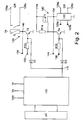
- FIG. 1 For example, a monitoring circuit 100 for monitoring a voltage Vdd by means of a comparator circuit is shown.
- the voltage Vdd is applied across a first voltage divider 102, which is formed by a series connection of the resistors R1 and R2, and is divided at the voltage divider 102 such that the electric potential V + is present at a tap 106 between the two resistors R1, R2.
- a second voltage divider 104 is connected, which comprises a series connection of the resistors R4 and R5.
- the voltage Vdd is divided so that at a tap 108 between the resistors R4, R5 the electrical potential becomes V-.
- the comparator circuit comprises two comparators CP1 and CP2 whose outputs can assume the states "high” and “low” and which are connected in the manner of a window comparator.
- the inverting input of the comparator CP1 is connected to the tap 106 of the voltage divider 102, so that the electrical potential V + is present there.
- the non-inverting input is connected via a resistor R7 to the point 110 at which a reference potential Vref is present.
- the output of the comparator CP1 is fed back via a resistor R8 to the non-inverting input.
- a positive feedback is achieved, which leads to a switching hysteresis.
- the switching hysteresis is determined by the resistors R7 and R8 and prevents a constant swinging of the comparator CP1 when the potential V + oscillates with small excursions by the value of the reference potential Vref.
- the inverting input of the second comparator CP2 is connected to the point 112, at which the reference potential Vref is likewise present.
- the non-inverting input is connected to the tap 108 of the voltage divider 104, at which the electrical potential V- is present.
- a positive feedback is achieved in that the output of the comparator CP2 is fed back via a resistor R9 to the non-inverting input. This also results in the comparator CP2 a switching hysteresis, which is determined by the resistor R9. The switching hysteresis prevents the comparator CP2 from continuously swinging when the potential V- shifts with small excursions by the value of the reference potential Vref.
- the switching hysteresis in the comparator CP1 and / or in the comparator CP2 can be dispensed with without impairing the operating principle of the monitoring circuit 100 as such.
- the feedback branch with the resistor R8 drops off when the hysteresis is omitted.
- the feedback branch with resistor R9 drops off when no hysteresis is desired.
- the reference potential Vref is derived in the illustrated embodiment of the monitoring circuit 100 by means of a Zener diode D1 as accurate as possible from a supply voltage Vs. In a simple manner, this ensures that the reference potential Vref can be set to a predetermined value with high accuracy even when the supply voltage Vs fluctuates. This means that the supply voltage Vs may be subject to fluctuations without affecting the functions or reliability of the monitoring circuit 100.
- the supply voltage Vs is applied across a series circuit of the zener diode D1 and a resistor R10, wherein the zener diode D1 is connected between the resistor R10 and ground potential. This is present at points 110 and 112 between zener diode D1 and resistor R10 Reference potential Vref thus corresponds to the voltage drop across the zener diode D1.
- the output of the comparator CP1 is switched to "high” as long as the potential V + is less than the reference potential Vref.
- the comparator CP1 switches the output to "low” when the potential V + exceeds the value of the reference potential Vref. This is the case when the voltage Vdd to be monitored is the value Vdd .
- H 1 + R ⁇ 1 R ⁇ 2 ⁇ Vref exceeds.
- the state "high” is present at the output of the comparator CP2 as long as the potential V- is greater than the reference potential Vref.
- the output of the comparator CP2 switches to the state "low” when the potential V- falls below the value of the reference potential Vref. It is calculated that this is the case when the voltage to be monitored Vdd is the value Vdd .
- L 1 + R ⁇ 4 R ⁇ 5 ⁇ Vref below.
- the value to be undershot is lower and additionally depends on the resistance R9. The greater the resistance R9, the smaller the deviation from the value Vdd, L indicated in equation (2), and thus also the switching hysteresis.
- the outputs of the two comparators CP1, CP2 are switched to "high" as long as the monitored voltage Vdd is between the values Vdd, L and Vdd, H. These correspond to the intended Limits of the voltage Vdd and are set by a suitable choice of the resistors R1, R2, R4, R5 and the reference potential Vref. Vdd, L is the lower limit and Vdd, H is the upper limit. If there is a faulty voltage, then one of the comparators CP1, CP2 switches the output to "low". In the case of an overvoltage this is the comparator CP1 and in the case of undervoltage the comparator CP2.
- an open-collector circuit 114 is provided, in which so-called open-collector outputs of the comparators CP1, CP2 are used. In the “low” state, these outputs are connected to ground potential; in the "high” state, the connection to the ground potential is interrupted.
- the outputs of the comparators CP1, CP2 are connected to a potential Vt via a pull-up resistor. This is preferably positive and may for example correspond to the voltage Vdd to be monitored or the supply voltage Vs, so that no further voltage has to be generated. However, another potential could also be provided here.
- the outputs of the comparators CP1, CP2 are connected to the output 116 of the monitoring circuit 100. Between the output 116 of the monitoring circuit 100 and the ground potential, an output voltage Ua of the monitoring circuit 100 can be detected.
- the output voltage Ua is different from zero.
- the output voltage Ua is in the "high” state, in which there is a positive electrical potential at the output of the monitoring circuit 100.
- the output voltage Ua decreases State “low”, in which the output 116 of the monitoring circuit in the illustrated embodiment is at ground potential.
- the illustrated monitoring circuit 100 may be operated in a test mode to detect disturbances.
- a resistance of the voltage divider 102 may be changed to give a changed upper limit value Vdd, Htest, which exceeds the voltage Vdd even when no overvoltage exists.
- Vdd upper limit value
- Htest higher limit value
- a resistance of the voltage divider 104 may be changed to give a modified lower limit Vdd, Ltest, which is less than the voltage Vdd even when there is no undervoltage.
- Vdd lower limit
- Ltest lower limit
- a current path 118 is connected in parallel to the resistor R1.
- the current path 118 includes the series connection of a resistor R3 and a controllable switching element T1, with which the current path 118 can be closed.
- the switching element T1 is controlled by a microcontroller .mu.C.
- the switching element T1 is a transistor whose control terminal corresponds to the base terminal, which is driven via a series resistor R12.
- the microcontroller ⁇ C closes the current path 118 by means of the switching element T1, as a result of which the electrical potential V + at the point 106 changes. Without taking into account the switching hysteresis of the comparator CP1 and neglecting the voltage drop across the switching element T1, this results in the changed upper limit value Vdd .
- H - R ⁇ 1 2 R ⁇ 2 ⁇ R ⁇ 1 + R ⁇ 3 ⁇ Vref which is less than Vdd, H and is also referred to below as the upper test threshold.
- the resistor R3 is dimensioned such that the voltage Vdd exceeds the upper test threshold Vdd, Htest even if it is within the allowable range, ie, between the upper limit value Vdd, H and the lower limit value Vdd, L.
- a current path 120 is connected, which comprises a series connection of a resistor R6 and a controllable switching element T2.
- the switching element T2 is likewise controlled by the microcontroller .mu.C and, in the illustrated embodiment, is shown as a transistor with a control connection designed as a base. The control takes place in the illustrated embodiment via a series resistor R13.
- other known to those skilled switching elements can be used instead of a transistor.
- the switching element T2 is closed by the microcontroller .mu.C, so that the resistor R6 is connected in parallel to the resistor R5 of the voltage divider 104 and the electrical Potential V- changed at point 108. Without taking into account the switching hysteresis of the comparator CP2 and neglecting the voltage drop across the switching element T2, this results in the changed lower limit Vdd .
- L + R ⁇ 4 R ⁇ 6 ⁇ Vref which is greater than Vdd, L and is also referred to below as the lower test threshold.
- the resistor R6 is dimensioned such that the voltage Vdd falls below the lower test threshold Vdd, Ltest even if they are within the permitted range.
- the resistors in the voltage dividers 102 and 104 are thus changed by the parallel connection of the current paths 118 and 120 to resistors R1 and R5 to simulate fault voltages.
- the voltage dividers 102, 104 each comprise at least three resistors, wherein at least one resistor can be bridged by means of a switching element. As a result, the corresponding resistance is reduced and the resistance within the voltage divider is changed accordingly.
- Overvoltage and undervoltage are successively simulated in one embodiment. Starting from the normal operation of the circuit, a type of faulty voltage is first simulated and subsequently the other, wherein in each case it is checked whether the circuit reports a faulty voltage.
- the upper test threshold Vdd, Htest is preferably set by suitable dimensioning of the resistor R3 to have approximately the value of the lower limit value Vdd, L.
- the upper test threshold Vdd, Htest can be set to be no greater than the lower limit Vdd, L, and preferably just below the lower limit Vdd, L. This ensures that the output of the comparator CP1 provided for monitoring the upper limit value is set to "low". switches if no faulty voltage was reported before the simulation. In this case, the voltage Vdd is greater than the lower limit Vdd, L, provided that the circuit operates smoothly.
- the lower test threshold Vdd, Ltest is set by an appropriate dimensioning of the resistor R6 to be approximately equal to the upper limit value Vdd, H.
- the lower test threshold Vdd, Ltest can be set to be not less than the upper limit Vdd, H and preferably just above the upper limit Vdd, H.
- test thresholds Vdd, Htest and Vdd, Ltest in this case may have approximately the same value, wherein the upper test threshold Vdd, Htest should not be greater than the lower test threshold Vdd, Ltest, thus ensuring that the voltage Vdd is either greater when the upper test threshold Vdd, Htest or less than the lower test threshold Vdd, Ltest and the output of one of the comparators CP1, CP2 switches to "low", unless the circuit is disturbed.
- a simultaneous simulation of an overvoltage and undervoltage can be carried out when the outputs of the comparators CP1, CP2 are monitored independently of one another, which is also possible in an alternative embodiment of the circuit arrangement, which is not illustrated in the figures.
- FIG. 2 illustrates the use of the above-described monitoring circuit 100 in a controller with safe outputs QR and QS and to control equipment or devices, such as motors.
- the outputs are controlled by one or more microcontrollers to perform control tasks.
- One of the microcontrollers may be the microcontroller ⁇ C provided for the simulation of fault voltages.
- further microcontroller may be provided, which are not shown in the figure.
- the voltage Vdd to be monitored can be, for example, the supply voltage of the microcontroller contained in the control unit. Usually, this must be between 4.5 V and 5.5 V for microcontrollers, for example, in order to ensure perfect functioning of the microcontroller.
- the terminals 126a and 126b of the output QR can be connected to a load circuit which can be controlled by means of a relay S, in particular switched on and off.
- the relay S is controlled by a controllable switching element T3, which is connected in series with the relay S within a control circuit 130, wherein the supply voltage Vs of the control unit is applied across the series circuit.
- the switching element T3 in the illustrated embodiment is again a transistor. However, other controllable switching elements known to those skilled in the art can also be used.
- the switching element T3 As long as the switching element T3 is turned on, a current flows through the relay S, so that the load circuit is closed at the output QR.
- control current When switching off the switching element T3 of the current flowing through the relay S control current is interrupted, so that the relay S is turned off.
- the output QR is turned off, that is, the load circuit is interrupted.
- the switching element T3 can be acted upon via a series resistor R15 with a control signal which is provided via a terminal 122. This is connected to the microcontrollers of the controller to perform the intended control tasks.
- the output QS is controlled by means of an output driver 132, which in the illustrated embodiment has two output terminals 128a, 128b. In general, any number of output ports can be provided; In particular, four output terminals are customary.
- the output driver 132 is controlled via control terminals 129a, b by the microcontrollers of the controller to perform the intended control tasks.
- the power supply of the output driver 132 is provided via the supply circuit 142.
- the supply circuit 142 includes a supply transistor T, which is, for example, a MOSFET. Via the supply transistor T, a supply voltage is supplied to the output driver 132, which can also be the supply voltage Vs of the control unit.
- the supply transistor T When the supply transistor T is turned off, the power supply of the output driver 132 is interrupted and the output QS is turned off.
- the supply transistor T is controlled by a switching element T4, wherein the terminal of the supply transistor T, that is, when using a MOSFET whose gate terminal is connected via a resistor R14 to the supply voltage Vs and via the switching element T4 to ground potential.
- the switching element T4 is again designed as a transistor in the illustrated embodiment; however, other controllable switching elements known to those skilled in the art can equally be used.
- the supply transistor T is a p-channel MOSFET.
- the switching element T4 As long as the switching element T4 is turned on, there is a voltage between the gate terminal and the source contact, so that the supply transistor T is turned on.
- the output driver 132 When switched on, the output driver 132 is supplied with energy via the supply transistor T.
- the switching element T4 As soon as the switching element T4 is switched off, the voltage between the gate terminal and the source contact decreases, and the supply transistor T goes into the blocking state.
- the power supply of the output driver 132 is interrupted, so that the output QS and the output terminals 128a, b are turned off Switching element T3, the switching element T4 can be supplied via a series resistor R16 with a control signal which is provided via a terminal 136 which is connected to the microcontrollers of the control unit to switch the output QS.
- the outputs QR and QS are switched off.
- the control terminals of the switching elements T3 and T4 are connected via an output stage to the output 116 of FIG FIG. 1 shown monitoring circuit 100 connected. Via the output stage, the switching elements T3 and T4 are switched off when a fault voltage is present, that is, when the output 116 of the monitoring circuit 100 is switched to "low”. If the output 116 of the monitoring circuit 100 is switched to "high”, then there is no influence on the control of the switching elements T3 and T4.
- an output stage is shown which comprises diodes D2 and D3, via which the control terminals of the switching elements T3 and T4 are connected to the output 116 of the monitoring circuit 100.
- diodes D2, D3 By a suitable polarity of the diodes D2, D3 is thereby achieved that the diodes D2, D3 go into the conductive state when the output 116 of the monitoring circuit 100 is in the "low” state, and that the diodes D2, D3 are in the off state when the output 116 of the monitoring circuit 100 is in the "high” state.
- the control terminals of the switching elements T3 and T4 are thus set to a low potential, in particular to ground potential, so that the switching elements T3 and T4 are switched off.
- the diode forward voltages are small enough so that the switching elements T3 and T4 can be safely switched off.
- the output stage can also be constructed in other ways, in particular by means of transistors, in order to carry out the function described above.
- a tap 134 for detecting the control voltage of the output driver 132 is provided.
- the microcontroller .mu.C is connected to the tap 134 and measures the control voltage of the output driver 132 during the simulation of a fault of the voltage to be monitored Vdd.
- the microcontroller .mu.C checks whether the voltage supply of the output driver 132 during the simulation of an overvoltage and during the simulation of an undervoltage is interrupted. If this is the case, then the monitoring circuit 100 operates properly. However, if the voltage supply of the output driver 132 is not interrupted, then the microcontroller .mu.C detects a malfunction of the monitoring circuit 100.
- the output driver 132 turns off the output QS during the simulation of a fault voltage.
- the microcontroller ⁇ C checks whether the load circuit at the output QS is interrupted. A fault in the monitoring circuit 100 is detected in this embodiment, if during the simulation of a fault voltage no interruption of the load circuit is detected.
- the microcontroller .mu.C controls the control current through the relay S during a simulation of a fault of the voltage to be monitored Vdd detectable. If this is interrupted during the simulation of a faulty voltage, then the monitoring circuit 100 operates trouble-free. However, if no interruption of the control current is detected, then the microcontroller .mu.C recognizes a malfunction of the monitoring circuit 100.
- the detection of the control current of the relay takes place by means of a current measuring circuit, which in FIG. 2 with reference to the tap 140 and the terminal 138 schematically is illustrated.
- the actual current measuring circuit can be realized in a manner known to those skilled in the art.
- a voltage measurement may be provided instead of a current measurement to determine an interruption of the power supply of the relay.
- it may also be provided at the relay output QR that a supply transistor is used for the purpose of interrupting the voltage.
- the interruption of the control current can be determined analogously as in the transistor output QS.
- the simulation of a fault voltage is preferably made periodically to continuously monitor the correct operation of the monitoring circuit 100.
- the duration of the simulation is predetermined and is preferably chosen not greater than 1 ms.
Landscapes
- Physics & Mathematics (AREA)
- General Physics & Mathematics (AREA)
- Emergency Protection Circuit Devices (AREA)
- Tests Of Electronic Circuits (AREA)
- Measurement Of Current Or Voltage (AREA)
Applications Claiming Priority (1)
| Application Number | Priority Date | Filing Date | Title |
|---|---|---|---|
| DE102008018642.2A DE102008018642B4 (de) | 2008-04-11 | 2008-04-11 | Überwachungsschaltung und Verfahren zum Prüfen der Schaltung |
Publications (3)
| Publication Number | Publication Date |
|---|---|
| EP2117094A2 true EP2117094A2 (fr) | 2009-11-11 |
| EP2117094A3 EP2117094A3 (fr) | 2014-01-08 |
| EP2117094B1 EP2117094B1 (fr) | 2022-08-24 |
Family
ID=40831385
Family Applications (1)
| Application Number | Title | Priority Date | Filing Date |
|---|---|---|---|
| EP09005080.8A Active EP2117094B1 (fr) | 2008-04-11 | 2009-04-07 | Commutation de surveillance et procédé de contrôle d'une commutation |
Country Status (3)
| Country | Link |
|---|---|
| EP (1) | EP2117094B1 (fr) |
| DE (1) | DE102008018642B4 (fr) |
| PL (1) | PL2117094T3 (fr) |
Cited By (3)
| Publication number | Priority date | Publication date | Assignee | Title |
|---|---|---|---|---|
| DE102016106531A1 (de) | 2016-04-08 | 2017-10-12 | Eaton Electrical Ip Gmbh & Co. Kg | Busteilnehmer und Verfahren zum Betreiben eines Busteilnehmers |
| EP3657288A1 (fr) * | 2018-11-26 | 2020-05-27 | Pilz GmbH & Co. KG | Surveillance sécurisée de la tension |
| CN112969930A (zh) * | 2018-11-08 | 2021-06-15 | 标致雪铁龙汽车股份有限公司 | 设备电流输出端的具有经监测漏电的开关元件的抑制装置 |
Citations (4)
| Publication number | Priority date | Publication date | Assignee | Title |
|---|---|---|---|---|
| EP1042679A1 (fr) | 1997-12-23 | 2000-10-11 | Thomson-Csf Sextant | Circuit electronique de surveillance de tension electrique |
| DE19927389A1 (de) | 1999-06-16 | 2000-12-28 | Bosch Gmbh Robert | Schaltung zum Detektieren eines unzulässig hohen Stromes in einer Endstufe |
| DE10127054A1 (de) | 2001-06-02 | 2002-12-19 | Bosch Gmbh Robert | Verfahren zur Überwachung einer Spannungsversorgung eines Steuergeräts in einem Kraftfahrzeug |
| DE10142011A1 (de) | 2001-08-28 | 2003-04-03 | Infineon Technologies Ag | Spannungssensor, Schaltungsanordnung mit einem Spannungssensor, sowie Verfahren zum Konfigurieren und Betreiben einer derartigen Schaltungsanordnung |
Family Cites Families (4)
| Publication number | Priority date | Publication date | Assignee | Title |
|---|---|---|---|---|
| JPS5725012A (en) * | 1980-07-22 | 1982-02-09 | Toshiba Corp | Overvoltage detecting circuit |
| JP3292359B2 (ja) * | 1995-04-19 | 2002-06-17 | 河村電器産業株式会社 | 単相3線式回路遮断器 |
| DE29721675U1 (de) * | 1997-11-26 | 1998-03-05 | Siemens AG, 80333 München | Vorrichtung für die Überprüfung der Funktion einer ein elektromagnetisches Schaltelement aufweisenden elektrischen Schaltung |
| US20030007300A1 (en) * | 2001-07-06 | 2003-01-09 | George Mazereeuw | Voltage controller |
-
2008
- 2008-04-11 DE DE102008018642.2A patent/DE102008018642B4/de active Active
-
2009
- 2009-04-07 EP EP09005080.8A patent/EP2117094B1/fr active Active
- 2009-04-07 PL PL09005080.8T patent/PL2117094T3/pl unknown
Patent Citations (4)
| Publication number | Priority date | Publication date | Assignee | Title |
|---|---|---|---|---|
| EP1042679A1 (fr) | 1997-12-23 | 2000-10-11 | Thomson-Csf Sextant | Circuit electronique de surveillance de tension electrique |
| DE19927389A1 (de) | 1999-06-16 | 2000-12-28 | Bosch Gmbh Robert | Schaltung zum Detektieren eines unzulässig hohen Stromes in einer Endstufe |
| DE10127054A1 (de) | 2001-06-02 | 2002-12-19 | Bosch Gmbh Robert | Verfahren zur Überwachung einer Spannungsversorgung eines Steuergeräts in einem Kraftfahrzeug |
| DE10142011A1 (de) | 2001-08-28 | 2003-04-03 | Infineon Technologies Ag | Spannungssensor, Schaltungsanordnung mit einem Spannungssensor, sowie Verfahren zum Konfigurieren und Betreiben einer derartigen Schaltungsanordnung |
Cited By (8)
| Publication number | Priority date | Publication date | Assignee | Title |
|---|---|---|---|---|
| DE102016106531A1 (de) | 2016-04-08 | 2017-10-12 | Eaton Electrical Ip Gmbh & Co. Kg | Busteilnehmer und Verfahren zum Betreiben eines Busteilnehmers |
| WO2017174338A1 (fr) | 2016-04-08 | 2017-10-12 | Eaton Electrical Ip Gmbh & Co. Kg | Élément de bus et procédé de fonctionnement d'un élément de bus |
| US11372796B2 (en) | 2016-04-08 | 2022-06-28 | Eaton Intelligent Power Limited | Bus subscriber and method for operating a bus subscriber |
| CN112969930A (zh) * | 2018-11-08 | 2021-06-15 | 标致雪铁龙汽车股份有限公司 | 设备电流输出端的具有经监测漏电的开关元件的抑制装置 |
| CN112969930B (zh) * | 2018-11-08 | 2024-02-20 | 标致雪铁龙汽车股份有限公司 | 设备电流输出端的具有经监测漏电的开关元件的抑制装置 |
| EP3657288A1 (fr) * | 2018-11-26 | 2020-05-27 | Pilz GmbH & Co. KG | Surveillance sécurisée de la tension |
| CN111220841A (zh) * | 2018-11-26 | 2020-06-02 | 皮尔茨公司 | 安全的电压监测 |
| US11005360B2 (en) | 2018-11-26 | 2021-05-11 | Pilz Gmbh & Co. Kg | Apparatus and method for monitoring a safety function of a machine or technical installation |
Also Published As
| Publication number | Publication date |
|---|---|
| PL2117094T3 (pl) | 2022-11-28 |
| EP2117094A3 (fr) | 2014-01-08 |
| DE102008018642B4 (de) | 2017-02-23 |
| EP2117094B1 (fr) | 2022-08-24 |
| DE102008018642A1 (de) | 2009-10-15 |
Similar Documents
| Publication | Publication Date | Title |
|---|---|---|
| DE102018217116B3 (de) | Hochvoltsystem und Verfahren zur Überwachung von Isolationsfehlern in einem Hochvoltsystem | |
| DE102018119727A1 (de) | Prüfen von MOS-Leistungsschaltern | |
| DE4441070C2 (de) | Sicherheitsschalteranordnung | |
| DE102007046483A1 (de) | Schaltungsanordnung zur Überwachung einer elektrischen Isolation | |
| DE102019103144A1 (de) | Einrichtung und Verfahren zur Überwachung der Zuverlässigkeit einer Zellenimpedanzmessung einer Batteriezelle | |
| EP0413938B1 (fr) | Circuit pour surveiller l'état de commutation d'un transistor de puissance | |
| EP2546852B1 (fr) | Relais de sécurité bistable | |
| EP0775332B1 (fr) | Ensemble commutateur de securite | |
| WO2009124884A1 (fr) | Procédé et dispositif de détection d'un dysfonctionnement dans un circuit de puissance en pont | |
| EP2117094B1 (fr) | Commutation de surveillance et procédé de contrôle d'une commutation | |
| DE10127054B4 (de) | Verfahren zur Überwachung einer Spannungsversorgung eines Steuergeräts in einem Kraftfahrzeug | |
| EP1032519B1 (fr) | Cablage pour un composant de reglage, et procede de controle de ce cablage de composant de reglage | |
| DE3836690C1 (en) | Device for the interrogation of a sensor in a motor vehicle | |
| DE19508841C2 (de) | Sicherheitsschalteranordnung | |
| DE4232720C1 (de) | Anordnung zur Funktionsüberwachung und Meßwertauswertung von Füllstands-Sensoren, insbesondere Vibrations-Füllstands-Grenzschaltern | |
| EP2876509B1 (fr) | Commande de sécurité | |
| EP1329731B1 (fr) | Circuit d'attaque | |
| DE102020131060A1 (de) | Intelligenter elektronischer schalter | |
| DE102019113139A1 (de) | Vorrichtung und Verfahren zur Stromsteuerung eines Aktuators | |
| DE10034866C2 (de) | Schaltungsanordnung | |
| DE102020210339B4 (de) | Schaltungsanordnung und Verfahren zur Fehlererkennung | |
| DE10244534B4 (de) | Schaltungsanordnung sowie Verfahren zur Erkennung von Fehlersituationen in gekoppelten Systemen | |
| DE4402017C2 (de) | Verfahren zum fehlersicheren Überwachen einer Versorgungsspannung und Einrichtung zur Durchführung des Verfahrens | |
| DE102008029679B4 (de) | System, Verfahren und elektronische Schaltung für mindestens eine elektronische Schaltungseinheit | |
| DE4242936A1 (de) | Sicherheitseinrichtung mit Mikroprozessor |
Legal Events
| Date | Code | Title | Description |
|---|---|---|---|
| PUAI | Public reference made under article 153(3) epc to a published international application that has entered the european phase |
Free format text: ORIGINAL CODE: 0009012 |
|
| AK | Designated contracting states |
Kind code of ref document: A2 Designated state(s): AT BE BG CH CY CZ DE DK EE ES FI FR GB GR HR HU IE IS IT LI LT LU LV MC MK MT NL NO PL PT RO SE SI SK TR |
|
| RAP1 | Party data changed (applicant data changed or rights of an application transferred) |
Owner name: EATON INDUSTIES GMBH |
|
| RAP1 | Party data changed (applicant data changed or rights of an application transferred) |
Owner name: EATON INDUSTRIES GMBH |
|
| PUAL | Search report despatched |
Free format text: ORIGINAL CODE: 0009013 |
|
| AK | Designated contracting states |
Kind code of ref document: A3 Designated state(s): AT BE BG CH CY CZ DE DK EE ES FI FR GB GR HR HU IE IS IT LI LT LU LV MC MK MT NL NO PL PT RO SE SI SK TR |
|
| AX | Request for extension of the european patent |
Extension state: AL BA RS |
|
| RIC1 | Information provided on ipc code assigned before grant |
Ipc: H02H 3/04 20060101AFI20131202BHEP Ipc: H02H 3/20 20060101ALI20131202BHEP Ipc: G01R 19/165 20060101ALI20131202BHEP |
|
| 17P | Request for examination filed |
Effective date: 20140911 |
|
| RBV | Designated contracting states (corrected) |
Designated state(s): AT BE BG CH CY CZ DE DK EE ES FI FR GB GR HR HU IE IS IT LI LT LU LV MC MK MT NL NO PL PT RO SE SI SK TR |
|
| RAP1 | Party data changed (applicant data changed or rights of an application transferred) |
Owner name: EATON ELECTRICAL IP GMBH & CO. KG |
|
| 17Q | First examination report despatched |
Effective date: 20160803 |
|
| STAA | Information on the status of an ep patent application or granted ep patent |
Free format text: STATUS: EXAMINATION IS IN PROGRESS |
|
| RAP1 | Party data changed (applicant data changed or rights of an application transferred) |
Owner name: EATON INTELLIGENT POWER LIMITED |
|
| STAA | Information on the status of an ep patent application or granted ep patent |
Free format text: STATUS: EXAMINATION IS IN PROGRESS |
|
| STAA | Information on the status of an ep patent application or granted ep patent |
Free format text: STATUS: EXAMINATION IS IN PROGRESS |
|
| GRAP | Despatch of communication of intention to grant a patent |
Free format text: ORIGINAL CODE: EPIDOSNIGR1 |
|
| STAA | Information on the status of an ep patent application or granted ep patent |
Free format text: STATUS: GRANT OF PATENT IS INTENDED |
|
| RIC1 | Information provided on ipc code assigned before grant |
Ipc: G01R 35/00 20060101ALI20220318BHEP Ipc: G01R 19/165 20060101ALI20220318BHEP Ipc: H02H 3/20 20060101ALI20220318BHEP Ipc: H02H 3/04 20060101AFI20220318BHEP |
|
| INTG | Intention to grant announced |
Effective date: 20220408 |
|
| GRAS | Grant fee paid |
Free format text: ORIGINAL CODE: EPIDOSNIGR3 |
|
| GRAA | (expected) grant |
Free format text: ORIGINAL CODE: 0009210 |
|
| STAA | Information on the status of an ep patent application or granted ep patent |
Free format text: STATUS: THE PATENT HAS BEEN GRANTED |
|
| AK | Designated contracting states |
Kind code of ref document: B1 Designated state(s): AT BE BG CH CY CZ DE DK EE ES FI FR GB GR HR HU IE IS IT LI LT LU LV MC MK MT NL NO PL PT RO SE SI SK TR |
|
| REG | Reference to a national code |
Ref country code: GB Ref legal event code: FG4D Free format text: NOT ENGLISH |
|
| REG | Reference to a national code |
Ref country code: CH Ref legal event code: EP |
|
| REG | Reference to a national code |
Ref country code: IE Ref legal event code: FG4D Free format text: LANGUAGE OF EP DOCUMENT: GERMAN |
|
| REG | Reference to a national code |
Ref country code: AT Ref legal event code: REF Ref document number: 1514320 Country of ref document: AT Kind code of ref document: T Effective date: 20220915 Ref country code: DE Ref legal event code: R096 Ref document number: 502009016433 Country of ref document: DE |
|
| REG | Reference to a national code |
Ref country code: NL Ref legal event code: FP |
|
| REG | Reference to a national code |
Ref country code: LT Ref legal event code: MG9D |
|
| PG25 | Lapsed in a contracting state [announced via postgrant information from national office to epo] |
Ref country code: SE Free format text: LAPSE BECAUSE OF FAILURE TO SUBMIT A TRANSLATION OF THE DESCRIPTION OR TO PAY THE FEE WITHIN THE PRESCRIBED TIME-LIMIT Effective date: 20220824 Ref country code: PT Free format text: LAPSE BECAUSE OF FAILURE TO SUBMIT A TRANSLATION OF THE DESCRIPTION OR TO PAY THE FEE WITHIN THE PRESCRIBED TIME-LIMIT Effective date: 20221226 Ref country code: NO Free format text: LAPSE BECAUSE OF FAILURE TO SUBMIT A TRANSLATION OF THE DESCRIPTION OR TO PAY THE FEE WITHIN THE PRESCRIBED TIME-LIMIT Effective date: 20221124 Ref country code: LV Free format text: LAPSE BECAUSE OF FAILURE TO SUBMIT A TRANSLATION OF THE DESCRIPTION OR TO PAY THE FEE WITHIN THE PRESCRIBED TIME-LIMIT Effective date: 20220824 Ref country code: LT Free format text: LAPSE BECAUSE OF FAILURE TO SUBMIT A TRANSLATION OF THE DESCRIPTION OR TO PAY THE FEE WITHIN THE PRESCRIBED TIME-LIMIT Effective date: 20220824 Ref country code: FI Free format text: LAPSE BECAUSE OF FAILURE TO SUBMIT A TRANSLATION OF THE DESCRIPTION OR TO PAY THE FEE WITHIN THE PRESCRIBED TIME-LIMIT Effective date: 20220824 Ref country code: ES Free format text: LAPSE BECAUSE OF FAILURE TO SUBMIT A TRANSLATION OF THE DESCRIPTION OR TO PAY THE FEE WITHIN THE PRESCRIBED TIME-LIMIT Effective date: 20220824 |
|
| PG25 | Lapsed in a contracting state [announced via postgrant information from national office to epo] |
Ref country code: IS Free format text: LAPSE BECAUSE OF FAILURE TO SUBMIT A TRANSLATION OF THE DESCRIPTION OR TO PAY THE FEE WITHIN THE PRESCRIBED TIME-LIMIT Effective date: 20221224 Ref country code: HR Free format text: LAPSE BECAUSE OF FAILURE TO SUBMIT A TRANSLATION OF THE DESCRIPTION OR TO PAY THE FEE WITHIN THE PRESCRIBED TIME-LIMIT Effective date: 20220824 Ref country code: GR Free format text: LAPSE BECAUSE OF FAILURE TO SUBMIT A TRANSLATION OF THE DESCRIPTION OR TO PAY THE FEE WITHIN THE PRESCRIBED TIME-LIMIT Effective date: 20221125 |
|
| PG25 | Lapsed in a contracting state [announced via postgrant information from national office to epo] |
Ref country code: RO Free format text: LAPSE BECAUSE OF FAILURE TO SUBMIT A TRANSLATION OF THE DESCRIPTION OR TO PAY THE FEE WITHIN THE PRESCRIBED TIME-LIMIT Effective date: 20220824 Ref country code: DK Free format text: LAPSE BECAUSE OF FAILURE TO SUBMIT A TRANSLATION OF THE DESCRIPTION OR TO PAY THE FEE WITHIN THE PRESCRIBED TIME-LIMIT Effective date: 20220824 Ref country code: CZ Free format text: LAPSE BECAUSE OF FAILURE TO SUBMIT A TRANSLATION OF THE DESCRIPTION OR TO PAY THE FEE WITHIN THE PRESCRIBED TIME-LIMIT Effective date: 20220824 |
|
| REG | Reference to a national code |
Ref country code: DE Ref legal event code: R097 Ref document number: 502009016433 Country of ref document: DE |
|
| PG25 | Lapsed in a contracting state [announced via postgrant information from national office to epo] |
Ref country code: SK Free format text: LAPSE BECAUSE OF FAILURE TO SUBMIT A TRANSLATION OF THE DESCRIPTION OR TO PAY THE FEE WITHIN THE PRESCRIBED TIME-LIMIT Effective date: 20220824 Ref country code: EE Free format text: LAPSE BECAUSE OF FAILURE TO SUBMIT A TRANSLATION OF THE DESCRIPTION OR TO PAY THE FEE WITHIN THE PRESCRIBED TIME-LIMIT Effective date: 20220824 |
|
| P01 | Opt-out of the competence of the unified patent court (upc) registered |
Effective date: 20230521 |
|
| PLBE | No opposition filed within time limit |
Free format text: ORIGINAL CODE: 0009261 |
|
| STAA | Information on the status of an ep patent application or granted ep patent |
Free format text: STATUS: NO OPPOSITION FILED WITHIN TIME LIMIT |
|
| 26N | No opposition filed |
Effective date: 20230525 |
|
| PG25 | Lapsed in a contracting state [announced via postgrant information from national office to epo] |
Ref country code: SI Free format text: LAPSE BECAUSE OF FAILURE TO SUBMIT A TRANSLATION OF THE DESCRIPTION OR TO PAY THE FEE WITHIN THE PRESCRIBED TIME-LIMIT Effective date: 20220824 |
|
| PG25 | Lapsed in a contracting state [announced via postgrant information from national office to epo] |
Ref country code: LU Free format text: LAPSE BECAUSE OF NON-PAYMENT OF DUE FEES Effective date: 20230407 |
|
| REG | Reference to a national code |
Ref country code: BE Ref legal event code: MM Effective date: 20230430 |
|
| PG25 | Lapsed in a contracting state [announced via postgrant information from national office to epo] |
Ref country code: MC Free format text: LAPSE BECAUSE OF FAILURE TO SUBMIT A TRANSLATION OF THE DESCRIPTION OR TO PAY THE FEE WITHIN THE PRESCRIBED TIME-LIMIT Effective date: 20220824 |
|
| PG25 | Lapsed in a contracting state [announced via postgrant information from national office to epo] |
Ref country code: MC Free format text: LAPSE BECAUSE OF FAILURE TO SUBMIT A TRANSLATION OF THE DESCRIPTION OR TO PAY THE FEE WITHIN THE PRESCRIBED TIME-LIMIT Effective date: 20220824 |
|
| REG | Reference to a national code |
Ref country code: IE Ref legal event code: MM4A |
|
| PG25 | Lapsed in a contracting state [announced via postgrant information from national office to epo] |
Ref country code: BE Free format text: LAPSE BECAUSE OF NON-PAYMENT OF DUE FEES Effective date: 20230430 |
|
| PG25 | Lapsed in a contracting state [announced via postgrant information from national office to epo] |
Ref country code: IE Free format text: LAPSE BECAUSE OF NON-PAYMENT OF DUE FEES Effective date: 20230407 |
|
| PGFP | Annual fee paid to national office [announced via postgrant information from national office to epo] |
Ref country code: NL Payment date: 20240320 Year of fee payment: 16 |
|
| PG25 | Lapsed in a contracting state [announced via postgrant information from national office to epo] |
Ref country code: IE Free format text: LAPSE BECAUSE OF NON-PAYMENT OF DUE FEES Effective date: 20230407 |
|
| PGFP | Annual fee paid to national office [announced via postgrant information from national office to epo] |
Ref country code: GB Payment date: 20240320 Year of fee payment: 16 |
|
| PGFP | Annual fee paid to national office [announced via postgrant information from national office to epo] |
Ref country code: PL Payment date: 20240323 Year of fee payment: 16 Ref country code: IT Payment date: 20240320 Year of fee payment: 16 Ref country code: FR Payment date: 20240320 Year of fee payment: 16 |
|
| REG | Reference to a national code |
Ref country code: AT Ref legal event code: MM01 Ref document number: 1514320 Country of ref document: AT Kind code of ref document: T Effective date: 20230407 |
|
| PGFP | Annual fee paid to national office [announced via postgrant information from national office to epo] |
Ref country code: DE Payment date: 20240320 Year of fee payment: 16 |
|
| PGFP | Annual fee paid to national office [announced via postgrant information from national office to epo] |
Ref country code: CH Payment date: 20240501 Year of fee payment: 16 |
|
| PG25 | Lapsed in a contracting state [announced via postgrant information from national office to epo] |
Ref country code: AT Free format text: LAPSE BECAUSE OF NON-PAYMENT OF DUE FEES Effective date: 20230407 |
|
| PG25 | Lapsed in a contracting state [announced via postgrant information from national office to epo] |
Ref country code: AT Free format text: LAPSE BECAUSE OF NON-PAYMENT OF DUE FEES Effective date: 20230407 |
|
| PG25 | Lapsed in a contracting state [announced via postgrant information from national office to epo] |
Ref country code: BG Free format text: LAPSE BECAUSE OF FAILURE TO SUBMIT A TRANSLATION OF THE DESCRIPTION OR TO PAY THE FEE WITHIN THE PRESCRIBED TIME-LIMIT Effective date: 20220824 |
|
| PG25 | Lapsed in a contracting state [announced via postgrant information from national office to epo] |
Ref country code: BG Free format text: LAPSE BECAUSE OF FAILURE TO SUBMIT A TRANSLATION OF THE DESCRIPTION OR TO PAY THE FEE WITHIN THE PRESCRIBED TIME-LIMIT Effective date: 20220824 |