EP2101279A2 - Adjustable circuit and RFID reader unit - Google Patents
Adjustable circuit and RFID reader unit Download PDFInfo
- Publication number
- EP2101279A2 EP2101279A2 EP09003451A EP09003451A EP2101279A2 EP 2101279 A2 EP2101279 A2 EP 2101279A2 EP 09003451 A EP09003451 A EP 09003451A EP 09003451 A EP09003451 A EP 09003451A EP 2101279 A2 EP2101279 A2 EP 2101279A2
- Authority
- EP
- European Patent Office
- Prior art keywords
- signal
- path
- input
- oscillator
- circuit according
- Prior art date
- Legal status (The legal status is an assumption and is not a legal conclusion. Google has not performed a legal analysis and makes no representation as to the accuracy of the status listed.)
- Withdrawn
Links
Images


Classifications
-
- H—ELECTRICITY
- H04—ELECTRIC COMMUNICATION TECHNIQUE
- H04B—TRANSMISSION
- H04B1/00—Details of transmission systems, not covered by a single one of groups H04B3/00 - H04B13/00; Details of transmission systems not characterised by the medium used for transmission
- H04B1/38—Transceivers, i.e. devices in which transmitter and receiver form a structural unit and in which at least one part is used for functions of transmitting and receiving
- H04B1/40—Circuits
- H04B1/50—Circuits using different frequencies for the two directions of communication
- H04B1/52—Hybrid arrangements, i.e. arrangements for transition from single-path two-direction transmission to single-direction transmission on each of two paths or vice versa
- H04B1/525—Hybrid arrangements, i.e. arrangements for transition from single-path two-direction transmission to single-direction transmission on each of two paths or vice versa with means for reducing leakage of transmitter signal into the receiver
-
- G—PHYSICS
- G06—COMPUTING OR CALCULATING; COUNTING
- G06K—GRAPHICAL DATA READING; PRESENTATION OF DATA; RECORD CARRIERS; HANDLING RECORD CARRIERS
- G06K7/00—Methods or arrangements for sensing record carriers, e.g. for reading patterns
- G06K7/10—Methods or arrangements for sensing record carriers, e.g. for reading patterns by electromagnetic radiation, e.g. optical sensing; by corpuscular radiation
- G06K7/10009—Methods or arrangements for sensing record carriers, e.g. for reading patterns by electromagnetic radiation, e.g. optical sensing; by corpuscular radiation sensing by radiation using wavelengths larger than 0.1 mm, e.g. radio-waves or microwaves
-
- G—PHYSICS
- G01—MEASURING; TESTING
- G01S—RADIO DIRECTION-FINDING; RADIO NAVIGATION; DETERMINING DISTANCE OR VELOCITY BY USE OF RADIO WAVES; LOCATING OR PRESENCE-DETECTING BY USE OF THE REFLECTION OR RERADIATION OF RADIO WAVES; ANALOGOUS ARRANGEMENTS USING OTHER WAVES
- G01S7/00—Details of systems according to groups G01S13/00, G01S15/00, G01S17/00
- G01S7/02—Details of systems according to groups G01S13/00, G01S15/00, G01S17/00 of systems according to group G01S13/00
- G01S7/03—Details of HF subsystems specially adapted therefor, e.g. common to transmitter and receiver
- G01S7/038—Feedthrough nulling circuits
-
- H—ELECTRICITY
- H04—ELECTRIC COMMUNICATION TECHNIQUE
- H04B—TRANSMISSION
- H04B5/00—Near-field transmission systems, e.g. inductive or capacitive transmission systems
- H04B5/70—Near-field transmission systems, e.g. inductive or capacitive transmission systems specially adapted for specific purposes
- H04B5/77—Near-field transmission systems, e.g. inductive or capacitive transmission systems specially adapted for specific purposes for interrogation
Definitions
- the present invention relates to an adjustable circuit for filtering a transmission channel of an RFID signal and for suppressing a carrier signal in the reception path between an input port and an output port.
- the invention relates to an RFID reader unit with a circuit according to the invention.
- RFID systems are used in many different areas of automatic identification. Particularly in the field of industrial automation, the use of RFID systems is advantageous.
- the growing demands of quality management and quality assurance in automated production can be easily realized with RFID systems.
- Production and measurement data can easily be stored and carried along in the production on the object itself. They are thus available and documented at any time on any object. This also makes the flexibilization of production possible.
- Production parameters can be stored on the object and directly read out in the respective street. Objects can be taken out of the series at any time and added later without confusion.
- a failure of the central computer also poses no problem with regard to the unambiguous identification and localization of the objects by the decentralized storage of the data on RFID tags ( Klaus Finkenzeller: RFID Handbook, 3rd edition, Carl Hanser Verlag, Münch s).
- RFID systems distinguish between coupled and microwave systems.
- coupled systems data is exchanged between the reader unit and the tag through capacitive or inductive coupling.
- These systems typically operate at the frequencies of 135 kHz or 13.56 MHz.
- microwave systems a feedback-free, electromagnetic coupling takes place via the far field of an antenna.
- the frequency ranges 860 - 930 MHz, 2.45 GHz and 5.8 GHz are used.
- the reader unit sends a constant, sinusoidal carrier signal (English: continuous wave , CW), which supplies the day with energy. Furthermore, part of the carrier signal is reflected during the day.
- the tag modulates the data to be transmitted onto the carrier signal, the data then being recognizable in the frequency spectrum as sidebands around the signal.
- a maximum transmission power of 2 W ERP ( equivalent radiated power ) and the modulation methods to be used are specified here.
- the backscatter method simultaneously sends the carrier signal and receives the tag response (duplex mode).
- This can be realized by the use of a circulator, as for example in connection with Fig. 1 described is.
- a crosstalk may occur between the transmit port and the receive path, which increases with decreasing isolation between transmit path and receive path.
- the height of the crosstalk or the isolation is an important system property and contributes greatly to the system dynamics.
- the crosstalk is in the range of 20 to 30 dB.
- a crosstalk may also result from reflections of the transmission signal at the common transmitting / receiving antenna, which are passed on by the circulator task according to the reception path. Such reflections may be due, for example, to slight antenna mismatches.
- crosstalk which can also be called crosstalk
- tag responses may be superimposed so that they are no longer error-free to demodulate. Therefore, measures to reduce the crosstalk have been considered.
- Known approaches for reducing the carrier signal level in the receive path are limited primarily to the suppression of the crosstalk between the transmit and the receive path. These include the use of two separate antennas for transmitting and receiving instead of a circulator and a combined transmit / receive antenna. This can be further improved by an optimal alignment of the individual antennas and by using damping elements at appropriate locations of the respective antenna housing, the crosstalk between the transmit and the receive path. Practical values are around - 40 dB.
- a disadvantage of this approach is the sensitivity of the crosstalk with respect to environmental influences in the vicinity of the system or the tag. These include, for example, larger reflecting surfaces, which lead to a large transmission factor between the transmitting and the receiving antenna, which can superimpose the weak tag response as an interference signal.
- the circuit can be extended by a fixed, parallel-connected component which, together with the equivalent switching parameter of the crosstalk, forms a resonant circuit with a resonant frequency at the operating frequency.
- the crosstalk for the operating frequency can be compensated by a few decades depending on the quality of the element used. This approach can be realized with the use of a few SMD components and is inexpensive.
- a disadvantage of this approach is first in the invariant frequency position of the compensation, whereby the use is limited to a single frequency.
- the compensation is still relatively inflexible with respect to changes to the transmitting and / or the receiving antenna.
- the compensation is narrowband, whereby a strong dependence of the absolute frequency position of the compensation of the manufacturing tolerances arises. As a result, the improvement in insulation actually achievable at the operating frequency can vary widely.
- variable values such as varactor diodes
- an effective suppression of the carrier signal for individual channels can be undertaken solely by the use of digital signal processing.
- the filtering requirements of a single operating channel are so high (the relative bandwidth of UHF RFID is 0.23 ⁇ , for example) that, in turn, only digital signal processing allows reliable filtering of a single operating channel.
- Circulators, directional couplers and variable phase shifters are described in US Pat. No. 6,603,391 B1 .
- WO 2006/088583 A2 US 2006/0098765 A1 respectively US 2008/0081551 A1 ,
- an object of the invention can be considered to provide an adjustable circuit for filtering a transmission channel of an RFID signal and for suppressing a carrier signal in the receiving path between an input port and an output port, in which a very good suppression of the carrier signal with low-cost means is possible.
- an RFID reader unit is to be created in which the carrier signal is effectively suppressed by inexpensive means.
- An adjustable circuit for filtering a transmission channel of an RFID signal and for suppressing a carrier signal in the receiving path between an input port and an output port comprises at least one adjustable oscillator for generating an oscillator signal. Furthermore, at least one input mixer stage cooperating with the oscillator is provided for mixing an input signal with the aid of the oscillator signal to an intermediate frequency. Finally, the circuit according to the invention has a blocking device arranged downstream of the input mixer stage or the input mixer stages for suppressing the carrier signal at the intermediate frequency.
- Another core idea of the invention can be considered to pre-allocate an especially high-quality blocking device for suppressing a carrier signal to an input mixer stage with which an input signal can be set to be mixed to an intermediate frequency.
- a significant advantage is that the high-quality barrier means a particularly good suppression of the carrier signal is achieved and that also the intermediate frequency with the help of the adjustable oscillator and the input mixer stage is suitable and suitable tuned to the locking device.
- the locking device in particular high-quality, band-stop filter on.
- a bandpass filter can be arranged upstream or downstream of this bandstop filter.
- the bandpass filter and the band rejection filter are suitably matched to each other.
- bandpass filters can be present, between which can be switched back and forth. Also possible is a plurality of band reject filters and to provide associated bandpass filters, which can be switched between the individual pairs.
- the signal filtered by the blocking device that is to say, for example, by the band-stop filter
- the signal filtered by the blocking device can be evaluated at the intermediate frequency.
- at least one output mixer stage is preferably arranged downstream of the band-stop filter.
- the blocking device in addition to or as an alternative to the bandstop filter, has a first bandpass filter for filtering a first sideband of the input signal and a second bandpass filter for filtering a second sideband of the input signal.
- a power divider is expediently provided for dividing an input signal between a first path and a second path.
- a power divider is provided for dividing an input signal between a first path and a second path, that at least one first adjustable oscillator is provided for generating a first oscillator signal that in the first path with the first oscillator cooperating first input mixer stage is present for mixing the input signal by means of the first oscillator signal to a first intermediate frequency that the first input mixer stage of the first bandpass filter for filtering the first sideband of the input signal at the first intermediate frequency is arranged downstream, that in the second path one with the first oscillator or a second oscillator cooperating second input mixer stage is present for mixing the input signal by means of the oscillator signal to a second intermediate frequency and that of the second input mixer stage of the second bandpass filter for filtering the second sideband of the input signal at the second intermediate frequency is arranged downstream.
- a high-quality band rejection filter can then be dispensed with in principle.
- the first bandpass filter has a first output mixer stage is arranged downstream and the second bandpass filter is followed by a second output mixer stage.
- the first bandpass filter and the second bandpass filter can be matched to one another such that they pass the corresponding sidebands of the signal as required, but block the carrier signal.
- the use of the adjustable oscillators and the input mixer stages also makes it possible, as a further advantageous variant, that the first bandpass filter and the second bandpass filter are identical components, for which purpose the corresponding oscillator frequencies must be suitably set.
- the input mixer stages and the output mixer stages are matched to the filter components, that is to say for example the bandstop filter and the bandpass filters, or to a downstream evaluation circuit.
- the input mixer stages are down-mixer stages and / or the output mixer stages are upstream mixer stages.
- At least one amplifying element in particular at least one separate amplifier, may be present between the input mixer stage or the input mixer stages and the blocking means.
- amplifying stages may also be present in the band elimination filter and / or the bandpass filters.
- each mixer stage is connected to a separate adjustable oscillator.
- the output mixer stage or the output mixer stages act together with the same oscillator as the input mixer stage or stages arranged in the same path.
- Another important aspect in the sizing of a transmission / reception system is the calculation of the input noise power N, which is directly proportional to the system bandwidth ⁇ f .
- Commercially available systems typically use surface acoustic filters (SAW filters) which pass the operating band.
- SAW filters surface acoustic filters
- the effective filter bandwidth can be reduced from the bandwidth of the operating channel to the effective channel bandwidth.
- the input noise can be reduced by a factor between 10 and 100 for each RFID systems at 868 MHz and 2.45 GHz.
- the reduction of the filter bandwidth from the SAW filter for the operating band to the frequency selective channel filter results in an improvement of the input noise by a factor between 10 and 100, depending on whether the RFID system is at 868 MHz or at 2.45 GHz with a respective channel bandwidth of works up to 500 kHz.
- the use of the highest quality channel filter for the operating band reduces the input noise power of the receiver in proportion to the ratio between the SAW filter for the operating band used in the prior art and the bandwidth of the operating channel according to this invention.
- the operating band is 3 MHz in Europe and 28 MHz in the USA, while the bandwidth of an operating channel is 200 kHz and 500 kHz, respectively a factor of 15 or 56 can be achieved.
- the invention can be realized with commercially available components and is much cheaper in terms of cost and personnel investment as a realization by means of digital signal processing. Only with a disproportionate high investment in computing power, for example, in a frequency-selective filtering by digital signal processing, a reaction time in a comparable order of magnitude possible as in the electrical channel filter described here.
- a compensation circuit for suppressing the crosstalk between a transmission path and a reception path of the RFID reader unit comprising means for coupling a signal component of a carrier signal from the transmission path in a compensation path, wherein the compensation path at least one variable phase shifter and at least a variable attenuator for varying the signal component in the phase or in the amplitude, a device for coupling the varied in phase and in amplitude signal component from the compensation path to the receiving path, a unit for determining the present in the receiving path crosstalk, and a control unit for the variable phase shifter and the variable attenuator, which is in signal communication with the existing crosstalk determination unit.
- the suppression of the crosstalk, ie the crosstalk, the carrier signal can be improved on the receiving path, so that a higher system Dynamics are enabled, resulting in a higher range or in a lower bit error rate at the same distance between the reader unit and the tag.
- the compensation path branches according to the invention at the device for decoupling from the transmission path and terminates at the device for coupling into the reception path.
- the unit for determining the existing crosstalk is also provided on the reception path.
- the variable phase shifter is suitably connected upstream of the variable attenuator, i. arranged closer to the transmission path than the attenuator.
- control unit can be set up such that it controls the variable phase shifter and the variable attenuator as a function of the existing crosstalk, but preferably also as a function of the carrier signal, for example its frequency.
- control unit can control the variable phase shifter and the variable attenuator so that the existing crosstalk is minimal.
- the unit for determining the crosstalk present in the receiving path expediently has a detector.
- the frequency-selective suppression of the crosstalk allows this circuit to be used in systems with multiple transmission channels.
- the compensation circuit according to the invention employs an analog and dynamic adaptation of the transmission characteristics of a parallel transmission path by means of the control unit, whereby independence of both manufacturing tolerances and discrete values of the possibly used SMD components can be achieved.
- Fast dynamic compensation can be achieved through the dynamic adjustment of the compensation path between read operations, which makes it possible to dynamically compensate for environmental influences such as larger reflective surfaces near the system or the tag during operation.
- the compensation circuit can also be used to improve the isolation between the transmitting and receiving antennas of a two or more antenna array.
- Another significant advantage of the circuit described is the improved noise characteristic of the receiver, which is based on the fact that, in suppressing the carrier signal, the noise caused by this strong signal is equally suppressed.
- the transmission path and the reception path can be coupled via a circulator to a common antenna. Accordingly, it is advantageous that a circulator is provided between the transmission path and the reception path, which leads to at least one transmission / reception antenna, the transmission path being between a transmission connection and the circulator and the reception path between the circulator and a reception connection.
- the transmission path and the reception path can be coupled via a directional coupler with a common antenna. Accordingly, it is advantageous for a directional coupler to be provided between the transmission path and the reception path, which leads to at least one transmission / reception antenna, the transmission path between a transmission connection and the directional coupler and the reception path between the directional coupler and a reception connection.
- an arrangement with two antennas can be provided, which can further reduce the crosstalk. Accordingly, it is in accordance with the invention that at least one transmitting antenna is provided at the transmitting path and at least one receiving antenna at the receiving path, the transmitting path being between a transmitting port and the transmitting antenna and the receiving path between the receiving antenna and a receiving port.
- the device for decoupling a signal component in particular with a defined power, to be a coupler or unbalanced power divider, and / or for the device to couple in the signal component varied in phase and in amplitude Coupler or unbalanced power divider is.
- the unit for determining the crosstalk present in the receiving path comprises a further coupler or unbalanced power divider and / or a power detector.
- the unit for determining the existing crosstalk, in particular its coupler or unbalanced power divider, is expediently arranged on the reception path, preferably between the device for coupling in the signal portion varied in phase and in amplitude, and the reception terminal.
- the production cost can be further reduced by the fact that at least one of the coupler or unbalanced power divider is constructed by coupled lines or the use of SMD components.
- At least one fixed phase shifter and / or at least one fixed attenuator is arranged in the compensation path.
- These fixed elements can be used to adapt the phase or the amplitude of the decoupled signal component to the dynamic range of the variable phase shifter and / or the variable attenuator.
- the fixed modules are conveniently connected upstream of the variable modules, i. they are arranged between the device for decoupling the signal component and the variable modules in the compensation path.
- At least one amplifier unit is arranged in the compensation path.
- This amplifier unit can serve to compensate for changes in the amplitude of the decoupled carrier signal, which arise, for example, by the coupling factors of the coupler.
- the amplifier unit is expediently arranged between the variable elements and the means for coupling the phase-and-amplitude varied signal component in the compensation path.
- the control unit preferably also serves to control the amplifier unit in the compensation path.
- a further advantageous embodiment of the invention is that an amplifier unit, optionally with an integrated regulation of the gain (Automatic Gain Control), is used in front of the power detector. This can increase the dynamic range of the power detector.
- This amplifier unit is part of the unit for determining the existing crosstalk and / or is between the coupler or power divider of this unit and the power detector of this unit.
- the power detector is formed by a semiconductor integrated circuit (so-called integrated circuit, IC).
- IC integrated circuit
- control unit is set up so that it adapts the compensation path, that is to say in particular the variable phase shifter and the variable damping element, if appropriate also the amplifier unit of the compensation path, between individual read operations of the RFID reader unit.
- control unit is set up so that the variable phase shifter and the variable attenuator iteratively through different combinations of attenuation and phase values, wherein after a pass, the value range of attenuation and phase to a determined in the run best value for the crosstalk is restricted and / or a discretization of the attenuation and phase values is refined.
- the invention also relates to an RFID reader unit with a compensation circuit according to the invention.
- the compensation circuit according to the invention can also be used in other transmitter / receiver circuits.
- a dynamic matching network for use in RFID systems, in particular with an electrical circulator, for generating a frequency-selective suppression of the crosstalk, which is produced via the circulator described.
- This frequency-selective suppression of the crosstalk causes the sidebands in the frequency spectrum surrounding the carrier signal, which contain the tag response, to be no longer overshadowed by the strong crosstalk, which in turn leads to an increase in the system dynamics by the additionally achieved suppression.
- This additionally achieved system dynamics in turn results in an increased range or alternatively in an improved signal-to-noise ratio (or a lower bit error rate) with the same range.
- the compensation circuit can be used to compensate for environmental influences on the antenna input reflection except for compensating for the resulting over the circulator crosstalk between the transmission and the reception path, for example, by larger, highly reflective surfaces in the vicinity of the operating unit, and also to a Restrict the system dynamics.
- the compensation circuit can also be used in systems where two separate antennas are used for transmission and reception.
- a compensating circuit for suppressing the crosstalk between the transmitting terminal and the receiving terminal can be provided via a circulator leading to at least one transmitting / receiving antenna, consisting of a coupler or unbalanced power divider for coupling a defined power of the carrier signal between the transmitting terminal and the circulator, a compensation path consisting of at least one variable phase shifter and a variable attenuator, a coupler or unbalanced power divider for coupling the amplitude and phase in the compensation path signal component of the carrier signal to the path between the circulator and the receiving terminal, a unit for determining the existing crosstalk, which may consist of another coupler or unbalanced power divider and a power detector, and a control unit.
- a compensation circuit for suppressing the crosstalk between the transmitting terminal and the receiving terminal can be provided via at least one transmitting antenna and at least one receiving antenna, consisting of a coupler or unbalanced power divider for coupling a defined power of the carrier signal between the transmitting terminal and the transmitting antenna Compensation path consisting of at least one variable phase shifter and a variable attenuator, a coupler or unbalanced power divider for coupling the amplitude and phase in the compensation path signal component of the carrier signal on the path between the receiving antenna and the receiving terminal, a unit for determining the existing crosstalk, the may consist of a further coupler or unbalanced power divider and a power detector, and a control unit.
- coupler or unbalanced power dividers are constructed by coupled lines or the use of SMD components.
- At least one fixed phase shifter and / or a fixed attenuator is used in the compensation path for adapting the phase or the amplitude of the coupled-out carrier signal to the dynamic range of the variable phase shifter or the variable attenuator.
- a further aspect of the invention lies in the fact that an amplifier unit is used in the compensation path in order to compensate for the changes in the amplitude of the coupled-out carrier signal which arise, for example, from the coupling factors of the couplers.
- an amplifier unit in a compensation circuit according to the invention for suppressing the crosstalk between the transmitting terminal and the receiving terminal, can be used in front of the power detector in order to increase the dynamic measuring range of the detector.
- the detector can be replaced by a semiconductor integrated circuit (so-called Integrated Circuits, IC).
- variable attenuator and an amplifier can also be realized in a simple variant by a variable gain amplifier.
- Fig. 1 shows a schematic representation of a circuit according to the prior art for the realization of a transmission / reception path for a backscatter method necessary duplex operation using a circulator.
- the reader arrangement shown there has a transmitting terminal 10, an antenna 14, a receiving terminal 12 and a circulator 16, which is arranged between the transmitting terminal 10 and the receiving terminal 12.
- the supply of the second mixer stage by the oscillator 314 via the signal divider 316 can be dispensed with or it can be replaced by a second oscillator.
- Fig. 2 shows schematically the structure of an embodiment of the electrically tunable channel filter according to the invention.
- This includes as essential components at least one adjustable oscillator 314, at least one signal divider 316 and at least two mixer stages 318 and 320.
- the input signal from the input terminal 310 is down-converted to an intermediate frequency by an oscillator signal of the variable oscillator 314 at a down-converter stage 318 and at the up-converter stage 320 mixed up again to the operating frequency.
- the carrier signal is suppressed by a high frequency band stop filter 322 and the respective operating channel is filtered by a band pass filter 324.
- amplification of the signal may be performed by an amplifier stage 326.
- the employed band rejection filter 322 and bandpass filter 324 have fixed frequencies.
- the task of the mixer stages is to mix the individual operating channels to the intermediate frequency and to mix the filtered signals from the intermediate frequency back to the original frequency position.
- the order of filtering and amplification is basically interchangeable. However, it is recommended to use a low-noise amplifier according to the amplification FIG. 2 This is preferable because it reduces the resulting chain noise figure and thus improves the signal-to-noise ratio.
- a further embodiment of the invention is to dispense with the second mixing stage and to carry out the further evaluation of the tag response at the intermediate frequency.
- either the supplies of the second mixer stages of the respective signal paths through the oscillators 414 and 416 via the signal dividers 438 and 440 can be dispensed with or they can be replaced by additional oscillators in each case.
- a separate filtering of the two sidebands of the tag response between the input port 410 and the output port 412 takes place.
- the input signal is divided by at least one signal divider 430 between the two signal paths.
- the oscillator signal in the first signal path in which, for example, the lower sideband can be filtered at a down-conversion stage 418 and an up-conversion stage 426 for the mixture, is provided by an oscillator 414 via a signal divider 438.
- the filtering of the first sideband is performed by the high-pass band pass filter 422, where the signal level can be optionally raised by a (low-noise) amplifier stage 434.
- filtering of the second sideband by the high-pass filter 424 with optional amplification by a (low-noise) amplifier stage 436 occurs on the second signal path.
- the oscillator signal required at the down-conversion stage 420 and the up-conversion stage 428 is provided by an oscillator 416 via a signal divider 440 generated.
- the merging of the two filtered sidebands from the two signal paths to a signal divider 432 produces a signal which essentially consists of the two sidebands or the tag response.
- the filters of the respective sidebands can be made at the same intermediate frequency, whereby the same electrical components can be used for the first and the second path.
- an evaluation of the tag response at any intermediate frequency can be performed by the use of additional oscillators for the second mixing stage of the respective sideband.
- Fig. 4 a schematically simplified construction of an embodiment of a compensation circuit 100 according to the invention is shown.
- This embodiment comprises at least one coupler 118, which decouples a defined power component of the carrier signal between the transmission port 110 and at least one circulator 116 to a parallel compensation path. It also comprises at least one coupler 118 ', which serves for coupling a defined power component of the signal manipulated in amplitude and phase from the compensation path to the reception path between the circulator 116 leading to the transmitting and receiving antenna 114 and the receiving port 112.
- a unit consisting of at least one coupler 118 ", which decouples a defined portion of the power between the coupler 118 'and the receiving port 112, and at least one further component, for example a detector 130, to determine the achieved suppression on the basis of the existing Power, wherein the further component forwards the determined power level to a control unit 132.
- the unwanted crosstalk is superimposed by an amplitude-equal, but shifted by 180 ° signal.
- a defined portion of the carrier signal originating from the transmitting terminal 110 coupled via the coupler 118 is varied in amplitude and phase by at least one variable phase shifter 124, at least one variable attenuator 126 and at least one amplifier unit 128 such that the superposition of this signal via the coupler 118 'with the existing over the circulator 116 and the transmitting / receiving antenna 114 crosstalk extinguished the crosstalk or at least compensated to a value below the sensitivity of the receiving unit.
- the couplers or asymmetrical power dividers 118, 118 'and 118 can be realized with concentrated components or so-called SMDs (Surface Mounted Devices)
- An alternative implementation of this coupler can be effected by distributed elements or coupled conductor segments.
- variable phase shifter 124 which may consist of both switchable discrete-value components and, for example, voltage-controlled chips with analog values
- at least one fixed phase shifter 120 may also be employed to adjust the phase response of the decoupled signal component to the dynamic range of the variable phase shifter.
- Such solid phase shifters 120 may be constructed as finished chips, as SMD components or as line elements.
- variable attenuator 126 which may be comprised of both discrete-value switchable components and analog-value voltage-controlled chips
- at least one fixed attenuator 122 may also be employed to adjust the amplitude of the coupled signal component to the dynamic range of the variable Attenuator 126 adapt.
- Such fixed attenuators 122 may be constructed, for example, as individual chips or as SMD components.
- the task of the control unit 132 is to evaluate the crosstalk detected by the power detector 130 and to set the phase and amplitude parameters required for the suppression in the individual modules 124, 126 on the compensation path.
- One possible algorithm for determining a good suppression of the crosstalk from the carrier signal to the receive path is to iterate through the different combinations of attenuation and phase values from the variable phase shifter 124 and the variable attenuator 126, with each pass through the range of values of the respective variable being set by the limited value and the discretization is refined.
- an amplifier unit 134 consisting of at least one amplifier, optionally with a self-regulating gain (so-called automatic gain control) can be used.
- Fig. 5 represents an alternative embodiment of the invention.
- the circulator and the combined transmitting / receiving antenna which are used in the front-end to implement the backscatter duplex operation necessary, by an antenna arrangement consisting of two separate antennas 214 ', 214 "for the Send or receive signal replaced.
- the crosstalk between the two antennas 214 ', 214 is comparable to the crosstalk over the circulator and can be equally suppressed by the use of the electrical compensation circuit described in this document.
- a directional coupler 116 ' may be used instead of a circulator.
- the input signal is applied to a first terminal 141 of the directional coupler 116 ', from where it is coupled to a second terminal 142 with a low loss of -0.3 dB. With a loss of -10 dB, the input signal is also coupled from the first terminal 141 to a third terminal 143 terminated with a terminating resistor to ground so that no reflections occur there. Finally, in the example shown, the signal coming from the antenna 114 is coupled with -10 dB loss to a fourth terminal 144 of the directional coupler 116 '.
- this embodiment is constructed as well as the variants described above. For clarity, the other ingredients in Fig. 6 omitted. In all figures, equivalent components are given the same reference numerals.
- Fig. 7 schematically shows an RFID reader unit 500 according to the invention.
- the RFID reader unit 500 includes a filter circuit 300 according to the invention, which is connected to the output 12 of the circulator 16.
- a compensation circuit 100 is connected in parallel with the circulator 16.
- a tunable in the frequency position filter circuit for suppressing a present in the RFID backscatter method carrier signal which simultaneously allows filtering of the operating channel by a highest quality band pass filter.
- the range of the RFID system can be increased more than 8 times, or at a constant distance, the bit error rate can be improved.
- the circuit described herein can be used in multi-channel RFID systems.
- the frequency position of the carrier signal can be changed dynamically to allow a greater frequency offset to other adjacent system or interferers.
- the analog circuit design based on components of the mass electronics ensures fast signal processing and cost-effective implementation.
- the electrically tunable carrier depressed channel filter described in this patent combines frequency selective analog carrier suppression with operational channel filtering and, in addition to the approaches described above, may be used for improved carrier suppression in the receive path.
- the improvement in carrier suppression results in a proportional improvement in system dynamics and, consequently, in increased range and / or bit error rate.
- the input noise is reduced, thus improving receiver sensitivity and signal-to-noise ratio.
- the invention described in this document allows a suppression of the crosstalk from the carrier signal in the input path combined with a simultaneous frequency-selective filtering of the operating channel, which is particularly necessary in a multi-reader environment.
- the system dynamics is increased by the suppression of the carrier signal caused thereby, resulting in an increase in the range or to improve the bit error rate at the same distance.
Landscapes
- Engineering & Computer Science (AREA)
- Toxicology (AREA)
- Physics & Mathematics (AREA)
- Health & Medical Sciences (AREA)
- General Physics & Mathematics (AREA)
- General Health & Medical Sciences (AREA)
- Artificial Intelligence (AREA)
- Computer Vision & Pattern Recognition (AREA)
- Electromagnetism (AREA)
- Theoretical Computer Science (AREA)
- Computer Networks & Wireless Communication (AREA)
- Signal Processing (AREA)
- Transceivers (AREA)
- Cable Transmission Systems, Equalization Of Radio And Reduction Of Echo (AREA)
- Transmitters (AREA)
- Noise Elimination (AREA)
Abstract
Description
Die vorliegende Erfindung betrifft in einem ersten Aspekt eine einstellbare Schaltung zum Filtern eines Übertragungskanals eines RFID-Signals und zum Unterdrücken eines Trägersignals im Empfangspfad zwischen einem Eingangstor und einem Ausgangstor. In einem zweiten Gesichtspunkt bezieht sich die Erfindung auf eine RFID-Readereinheit mit einer erfindungsgemäßen Schaltung.In a first aspect, the present invention relates to an adjustable circuit for filtering a transmission channel of an RFID signal and for suppressing a carrier signal in the reception path between an input port and an output port. In a second aspect, the invention relates to an RFID reader unit with a circuit according to the invention.
RFID-Systeme werden in unterschiedlichsten Bereichen der automatischen Identifikation eingesetzt. Besonders im Bereich der Industrieautomation ist der Einsatz von RFID-Systemen vorteilhaft. Die wachsenden Anforderungen des Qualitätsmanagements und der Qualitätssicherung in der automatischen Fertigung lassen sich mit RFID-Systemen gut realisieren. Fertigungs- und Messdaten können in der Produktion einfach am Objekt selbst hinterlegt und mitgeführt werden. Sie sind so zu jeder Zeit an jedem Objekt verfügbar und dokumentierbar. Dies ermöglicht auch die Flexibilisierung der Fertigung. Fertigungsparameter können am Objekt gespeichert und in der jeweiligen Straße direkt ausgelesen werden. Objekte können zu beliebigen Zeiten der Serie entnommen und später wieder hinzugefügt werden, ohne dass Verwechselungen entstehen. Ein Ausfall des Zentralrechners stellt im Bezug auf die eindeutige Identifizierung und Lokalisierung der Objekte durch die dezentrale Speicherung der Daten auf RFID-Tags ebenfalls kein Problem dar (
Prinzipiell unterschiedet man bei RFID-Systemen zwischen gekoppelten und Mikrowellen-Systemen. Bei den gekoppelten Systemen erfolgt der Datenaustausch zwischen der Readereinheit und dem Tag durch kapazitive bzw. induktive Kopplung. Diese Systeme arbeiten in der Regel bei den Frequenzen 135 kHz oder 13,56 MHz. Bei den Mikrowellensystemen erfolgt eine rückwirkungsfreie, elektromagnetische Kopplung über das Fernfeld einer Antenne. Hierbei werden die Frequenzbereiche 860 - 930 MHz, 2,45 GHz sowie 5,8 GHz eingesetzt.In principle, RFID systems distinguish between coupled and microwave systems. In the coupled systems, data is exchanged between the reader unit and the tag through capacitive or inductive coupling. These systems typically operate at the frequencies of 135 kHz or 13.56 MHz. In the microwave systems, a feedback-free, electromagnetic coupling takes place via the far field of an antenna. Here the frequency ranges 860 - 930 MHz, 2.45 GHz and 5.8 GHz are used.
Ein wesentlicher Teil der verfügbaren RFID-Systeme funktioniert nach dem so genannten Backscatter- (bzw. Rückstreuungs-) Verfahren. Bei diesen Systemen sendet die Readereinheit ein konstantes, sinusförmiges Trägersignal (engl. continuous wave, CW), welches den Tag mit Energie versorgt. Weiterhin wird ein Teil des Trägersignals am Tag reflektiert. Über eine Änderung der Antennen-Rückstreueigenschaften moduliert der Tag die zu übertragenden Daten auf das Trägersignal, wobei die Daten dann im Frequenzspektrum als Seitenbänder um das Signal erkennbar sind.An essential part of the available RFID systems works according to the so-called backscatter method. In these systems, the reader unit sends a constant, sinusoidal carrier signal (English: continuous wave , CW), which supplies the day with energy. Furthermore, part of the carrier signal is reflected during the day. By changing the antenna backscatter characteristics, the tag modulates the data to be transmitted onto the carrier signal, the data then being recognizable in the frequency spectrum as sidebands around the signal.
Anhand der bekannten Gleichungen für die Feldausbreitung können die wesentlichen Empfangs- und Sendeleistungen einer Übertragungsstrecke wie folgt beschrieben werden:
- 1. Funkfelddämpfung


- 2. Empfangsleistung nach der Tagantenne


- 3. Sendeleistung des Tags


- 4. Empfangsleistung an der Readereinheit


- 1. Radio field attenuation
- 2. Reception power after the tag antenna
- 3. Transmitting power of the tag
- 4. Receiving power at the reader unit
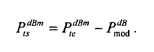
Weiterhin kann eine für die Entfernung erforderliche Systemdynamik D in Dezibel über die Differenz zwischen der Sendeleistung ![]()
![]()

![]()
![]()
In den Normen ISO-IEC 18000-6C sowie ETSI EN 302 208-1 sind die UHF RFID-Systeme im Frequenzbereich 860 MHz - 930 MHz reglementiert. Hierin werden beispielsweise eine maximale Sendeleistung von 2 W ERP (equivalent radiated power) sowie die einzusetzenden Modulationsverfahren vorgegeben.The ISO-IEC 18000-6C and ETSI EN 302 208-1 standards regulate the UHF RFID systems in the 860 MHz - 930 MHz frequency range. For example, a maximum transmission power of 2 W ERP ( equivalent radiated power ) and the modulation methods to be used are specified here.
Für eine Strecke von einem Meter ergibt sich hierdurch eine Funkfelddämpfung von ca. 31,2 dB, die sich bei jeder Verdopplung der Übertragungsstrecke um einen Faktor von 6 dB erhöht. Unter realistischen Bedingungen:
- ■ Sendeleistung 2 W ERP,
- ■ Betriebsfrequenz 866,5 MHz,
- ■ Antennengewinne der Readerantenne und der Tagantenne von jeweils 6 dBi und 1 dBi,
- ■ Modulationsverluste von 6 dB
- ■ sowie Reflexionsverluste von 0,5 dB
- ■ transmission power 2 W ERP,
- ■ operating frequency 866.5 MHz,
- Antenna gains of the reader antenna and the tag antenna of 6 dBi and 1 dBi each,
- ■ Modulation losses of 6 dB
- ■ and reflection losses of 0.5 dB
Beim Backscatter-Verfahren wird gleichzeitig das Trägersignal gesendet und die Tag-Antwort empfangen (Duplexbetrieb). Dies kann durch den Einsatz eines Zirkulators realisiert werden, wie er beispielsweise im Zusammenhang mit
Ein Übersprecher kann sich auch durch Reflexionen des Sendesignals an der gemeinsamen Sende-/Empfangsantenne ergeben, welche durch den Zirkulator aufgabengemäß an den Empfangspfad weitergegeben werden. Solche Reflexionen können beispielsweise auf geringfügigen Fehlanpassungen der Antenne beruhen.A crosstalk may also result from reflections of the transmission signal at the common transmitting / receiving antenna, which are passed on by the circulator task according to the reception path. Such reflections may be due, for example, to slight antenna mismatches.
Durch den Übersprecher, der auch als Crosstalk bezeichnet werden kann, können unter Umständen Tag-Antworten überlagert werden, so dass sie nicht mehr fehlerfrei zu demodulieren sind. Es sind daher Maßnahmen zur Reduzierung des Übersprechers erwogen worden.Due to the crosstalk, which can also be called crosstalk, tag responses may be superimposed so that they are no longer error-free to demodulate. Therefore, measures to reduce the crosstalk have been considered.
Bekannte Ansätze zur Reduzierung des Trägersignalpegels im Empfangspfad beschränken sich primär auf die Unterdrückung des Übersprechers zwischen dem Sende- und dem Empfangspfad. Hierzu zählt zunächst der Einsatz von zwei getrennten Antennen zum Senden und Empfangen anstelle eines Zirkulators und einer kombinierten Sende-/Empfangsantenne. Hierbei kann durch eine optimale Ausrichtung der einzelnen Antennen sowie durch Einsatz von Dämpfungselementen an geeigneten Stellen der jeweiligen Antennengehäuse der Übersprecher zwischen dem Sende-und dem Empfangspfad weiter verbessert werden. Praktische Werte liegen hierbei um - 40 dB.Known approaches for reducing the carrier signal level in the receive path are limited primarily to the suppression of the crosstalk between the transmit and the receive path. These include the use of two separate antennas for transmitting and receiving instead of a circulator and a combined transmit / receive antenna. This can be further improved by an optimal alignment of the individual antennas and by using damping elements at appropriate locations of the respective antenna housing, the crosstalk between the transmit and the receive path. Practical values are around - 40 dB.
Nachteilig bei dieser Vorgehensweise ist die Empfindlichkeit des Übersprechers bezüglich Umwelteinflüssen in der Nähe des Systems oder des Tags. Hierzu zählen zum Beispiel größere reflektierende Flächen, die zu einem großen Übertragungsfaktor zwischen der Sende- und der Empfangsantenne führen, der als Störsignal die schwache Tag-Antwort überlagern kann.A disadvantage of this approach is the sensitivity of the crosstalk with respect to environmental influences in the vicinity of the system or the tag. These include, for example, larger reflecting surfaces, which lead to a large transmission factor between the transmitting and the receiving antenna, which can superimpose the weak tag response as an interference signal.
Weiterhin kann die Schaltung durch ein festes, parallel geschaltetes Bauelement, das zusammen mit dem Ersatzschaltparameter des Übersprechers einen Resonanzkreis mit einer Resonanzfrequenz bei der Betriebsfrequenz bildet, erweitert werden. Dadurch kann der Übersprecher für die Betriebsfrequenz in Abhängigkeit der Güte des eingesetzten Elements um einige Dekaden kompensiert werden. Dieser Ansatz kann mit dem Einsatz von wenigen SMD-Komponenten realisiert werden und ist kostengünstig.Furthermore, the circuit can be extended by a fixed, parallel-connected component which, together with the equivalent switching parameter of the crosstalk, forms a resonant circuit with a resonant frequency at the operating frequency. As a result, the crosstalk for the operating frequency can be compensated by a few decades depending on the quality of the element used. This approach can be realized with the use of a few SMD components and is inexpensive.
Ein Nachteil dieses Vorgehens besteht zunächst in der invarianten Frequenzlage der Kompensation, wodurch der Einsatz auf eine einzige Frequenz beschränkt wird. Außerdem kann wegen der diskreten Werte der verfügbaren Komponenten nur ein geringes Maß an Kompensation erreicht werden. Die Kompensation ist im Hinblick auf Änderungen an der Sende- und/oder der Empfangsantenne weiterhin vergleichsweise unflexibel. Schließlich ist die Kompensation schmalbandig, wodurch eine starke Abhängigkeit der absoluten Frequenzlage der Kompensation von den Fertigungstoleranzen entsteht. Dies führt dazu, dass die tatsächlich bei der Betriebsfrequenz erreichbare Verbesserung der Isolation stark variieren kann.A disadvantage of this approach is first in the invariant frequency position of the compensation, whereby the use is limited to a single frequency. In addition, due to the discrete values of the available components, only a small amount of compensation can be achieved. The compensation is still relatively inflexible with respect to changes to the transmitting and / or the receiving antenna. Finally, the compensation is narrowband, whereby a strong dependence of the absolute frequency position of the compensation of the manufacturing tolerances arises. As a result, the improvement in insulation actually achievable at the operating frequency can vary widely.
Durch den Einsatz von Komponenten mit variablen Werten, wie beispielsweise Varaktordioden, kann eine gewisse Flexibilität bezüglich der Frequenzlage und der Kompensation eingeführt werden. Praktische Werte liegen hierbei um -35 dB.By using components with variable values, such as varactor diodes, some flexibility in terms of frequency position and compensation can be introduced. Practical values are -35 dB.
Es gibt weiterhin wenige Ansätze, um eine Unterdrückung des Trägersignals im Empfangspfad vorzunehmen: Durch den Einsatz einer digitalen Signalverarbeitung beispielsweise durch DSPs (Digital Signal Processors) ist eine schmalbandige Unterdrückung von bis zu - 80 dB möglich. Weiterhin können bei diesem Ansatz frequenzselektive Filter mit unterschiedlichen Bandbreiten realisiert werden.Furthermore, there are few approaches to suppression of the carrier signal in the receive path: By using digital signal processing, for example by DSPs (Digital Signal Processors), a narrowband suppression of up to -80 dB is possible. Furthermore, in this approach, frequency-selective filters with different bandwidths can be realized.
Nachteilig bei einer digitalen Signalverarbeitung ist einerseits der höhere Investitionsbedarf, sowohl für die Hardwareanschaffung als auch für die bei der Software-Erstellung benötigte Entwicklungszeit und die zugehörigen Kosten. Andererseits beansprucht die Hardware relativ viel Platz und ist, abhängig von den zu realisierenden Anforderungen, wesentlich langsamer als eine analoge Schaltung.A disadvantage of a digital signal processing on the one hand, the higher investment needs, both for the hardware purchase and for the development time required in the software development and the associated costs. On the other hand, the hardware takes up a relatively large amount of space and, depending on the requirements to be realized, is much slower than an analog circuit.
Eine weitere Möglichkeit zur Realisierung einer verbesserten Unterdrückung des Trägersignals im Empfangspfad wird in "System combining radio frequency transmitter and receiver using circulator and method for cancelling transmission signal thereof' (
Gemäß dem Stand der Technik kann allein durch den Einsatz einer digitalen Signalverarbeitung eine effektive Unterdrückung des Trägersignals für einzelne Kanäle vorgenommen werden. Die Anforderungen an einer Filterung eines einzelnen Betriebskanals sind so hoch (die relative Bandbreite bei UHF RFID beträgt beispielsweise 0,23 ‰), dass wiederum einzig eine digitale Signalverarbeitung eine zuverlässige Filterung eines einzigen Betriebskanals ermöglicht.According to the prior art, an effective suppression of the carrier signal for individual channels can be undertaken solely by the use of digital signal processing. The filtering requirements of a single operating channel are so high (the relative bandwidth of UHF RFID is 0.23 ‰, for example) that, in turn, only digital signal processing allows reliable filtering of a single operating channel.
Zirkulatoren, Richtkoppler und variable Phasenschieber sind beschrieben in
Als eine Aufgabe der Erfindung kann angesehen werden, eine einstellbare Schaltung zum Filtern eines Übertragungskanals eines RFID-Signals und zum Unterdrücken eines Trägersignals im Empfangspfad zwischen einem Eingangstor und einem Ausgangstor zu schaffen, bei dem eine sehr gute Unterdrückung des Trägersignals mit kostengünstigen Mitteln möglich ist. Außerdem soll eine RFID-Readereinheit geschaffen werden, bei der das Trägersignal mit kostengünstigen Mitteln effektiv unterdrückt wird.As an object of the invention can be considered to provide an adjustable circuit for filtering a transmission channel of an RFID signal and for suppressing a carrier signal in the receiving path between an input port and an output port, in which a very good suppression of the carrier signal with low-cost means is possible. In addition, an RFID reader unit is to be created in which the carrier signal is effectively suppressed by inexpensive means.
Diese Aufgabe wird erfindungsgemäß durch die einstellbare Schaltung mit den Merkmalen des Anspruchs 1 und durch eine RFID-Readereinheit gemäß Anspruch 13, bei welcher eine solche Schaltung eingesetzt wird, gelöst.This object is achieved by the adjustable circuit with the features of claim 1 and by an RFID reader unit according to claim 13, in which such a circuit is used, solved.
Bevorzugte Ausführungsbeispiele der erfindungsgemäßen Schaltung werden im Folgenden, insbesondere im Bezug auf die abhängigen Ansprüche und die Figuren, beschrieben.Preferred embodiments of the circuit according to the invention are described below, in particular with reference to the dependent claims and the figures.
Eine einstellbare Schaltung zum Filtern eines Übertragungskanals eines RFID-Signals und zum Unterdrücken eines Trägersignals im Empfangspfad zwischen einem Eingangstor und einem Ausgangstor weist erfindungsgemäß mindestens einen einstellbaren Oszillator zum Erzeugen eines Oszillatorsignals auf. Weiterhin ist mindestens eine mit dem Oszillator zusammenwirkende Eingangsmischerstufe zum Mischen eines Eingangssignals mit Hilfe des Oszillatorsignals auf eine Zwischenfrequenz vorhanden. Schließlich weist die erfindungsgemäße Schaltung eine der Eingangsmischerstufe oder den Eingangsmischerstufen nachgeordnete Sperreinrichtung zum Unterdrücken des Trägersignals bei der Zwischenfrequenz auf.An adjustable circuit for filtering a transmission channel of an RFID signal and for suppressing a carrier signal in the receiving path between an input port and an output port according to the invention comprises at least one adjustable oscillator for generating an oscillator signal. Furthermore, at least one input mixer stage cooperating with the oscillator is provided for mixing an input signal with the aid of the oscillator signal to an intermediate frequency. Finally, the circuit according to the invention has a blocking device arranged downstream of the input mixer stage or the input mixer stages for suppressing the carrier signal at the intermediate frequency.
Als ein erster Kerngedanke der Erfindung kann angesehen werden, zum Unterdrükken eines Trägersignals bei einer RFID-Einrichtung mit kostengünstigen Mitteln, nicht mehr, wie im Stand der Technik, Komponenten vorzusehen, welche für eine bestimmte Frequenz eingerichtet sind, sondern eine prinzipiell einstellbare Schaltung vorzusehen. Auf diese Weise wird eine deutlich erhöhte Flexibilität erreicht.As a first central idea of the invention, it can be considered, for suppressing a carrier signal in an RFID device with cost-effective means, not to provide, as in the prior art, components which are set up for a specific frequency, but to provide a circuit which can be set in principle. In this way, a significantly increased flexibility is achieved.
Als weiterer Kerngedanke der Erfindung kann erachtet werden, einer insbesondere qualitativ hochwertigen Sperreinrichtung zum Unterdrücken eines Trägersignals eine Eingangsmischerstufe vorzuordnen, mit welcher ein Eingangssignal einstellbar auf eine Zwischenfrequenz gemischt werden kann. Ein wesentlicher Vorteil ist dabei, dass durch die qualitativ hochwertige Sperreinrichtung eine besonders gute Unterdrückung des Trägersignals erreicht wird und dass außerdem die Zwischenfrequenz mit Hilfe des einstellbaren Oszillators und der Eingangsmischerstufe geeignet und passend auf die Sperreinrichtung abstimmbar ist.Another core idea of the invention can be considered to pre-allocate an especially high-quality blocking device for suppressing a carrier signal to an input mixer stage with which an input signal can be set to be mixed to an intermediate frequency. A significant advantage is that the high-quality barrier means a particularly good suppression of the carrier signal is achieved and that also the intermediate frequency with the help of the adjustable oscillator and the input mixer stage is suitable and suitable tuned to the locking device.
Bei einer besonders bevorzugten Ausführungsvariante der erfindungsgemäßen Schaltung weist die Sperreinrichtung ein, insbesondere hochgütiges, Bandsperrfilter auf.In a particularly preferred embodiment of the circuit according to the invention, the locking device, in particular high-quality, band-stop filter on.
Diesem Bandsperrfilter kann gemäß einer weiteren vorteilhaften Variante zum Filtern des Übertragungskanals bei der Zwischenfrequenz ein Bandpassfilter vor- oder nachgeordnet sein. Hierbei sind der Bandpassfilter und der Bandsperrfilter zweckmäßig aufeinander abgestimmt.According to a further advantageous variant for filtering the transmission channel at the intermediate frequency, a bandpass filter can be arranged upstream or downstream of this bandstop filter. Here, the bandpass filter and the band rejection filter are suitably matched to each other.
Prinzipiell können auch mehrere Bandpassfilter vorhanden sein, zwischen denen hin-und hergeschaltet werden kann. Ebenso ist möglich, eine Mehrzahl von Bandsperrfiltern und zugeordneten Bandpassfiltern vorzusehen, wobei zwischen den einzelnen Paaren umgeschaltet werden kann.In principle, several bandpass filters can be present, between which can be switched back and forth. Also possible is a plurality of band reject filters and to provide associated bandpass filters, which can be switched between the individual pairs.
Grundsätzlich kann das durch die Sperreinrichtung, also beispielsweise durch den Bandsperrfilter, gefilterte Signal bei der Zwischenfrequenz ausgewertet werden. Um jedoch auf kommerziell erhältliche Komponenten zur Auswertung der von den RFID-Tags gesendeten Informationen zurückgreifen zu können, ist es bevorzugt, das Ausgangssignal auf eine definierte Frequenz zu setzen. Hierzu ist bevorzugt dem Bandsperrfilter mindestens eine Ausgangsmischerstufe nachgeordnet.In principle, the signal filtered by the blocking device, that is to say, for example, by the band-stop filter, can be evaluated at the intermediate frequency. However, in order to be able to resort to commercially available components for evaluating the information sent by the RFID tags, it is preferable to set the output signal to a defined frequency. For this purpose, at least one output mixer stage is preferably arranged downstream of the band-stop filter.
Bei einer weiteren Variante der erfindungsgemäßen Schaltung weist die Sperreinrichtung ergänzend oder alternativ zu dem Bandsperrfilter ein erstes Bandpassfilter zum Filtern eines ersten Seitenbands des Eingangssignals und ein zweites Bandpassfilter zum Filtern eines zweiten Seitenbands des Eingangssignals auf. Zweckmäßig ist hierzu ein Leistungsteiler vorhanden zum Teilen eines Eingangssignals zwischen einem ersten Pfad und einem zweiten Pfad.In a further variant of the circuit according to the invention, the blocking device, in addition to or as an alternative to the bandstop filter, has a first bandpass filter for filtering a first sideband of the input signal and a second bandpass filter for filtering a second sideband of the input signal. For this purpose, a power divider is expediently provided for dividing an input signal between a first path and a second path.
Eine vorteilhafte Weiterentwicklung dieser Variante ist dadurch gekennzeichnet, dass ein Leistungsteiler vorhanden ist zum Teilen eines Eingangssignals zwischen einem ersten Pfad und einem zweiten Pfad, dass mindestens ein erster einstellbarer Oszillator vorhanden ist zum Erzeugen eines ersten Oszillatorsignals, dass im ersten Pfad eine mit dem ersten Oszillator zusammenwirkende erste Eingangsmischerstufe vorhanden ist zum Mischen des Eingangssignals mit Hilfe des ersten Oszillatorsignals auf eine erste Zwischenfrequenz, dass der ersten Eingangsmischerstufe der erste Bandpassfilter zum Filtern des ersten Seitenbands des Eingangssignals bei der ersten Zwischenfrequenz nachgeordnet ist, dass im zweiten Pfad eine mit dem ersten Oszillator oder einem zweiten Oszillator zusammenwirkende zweite Eingangsmischerstufe vorhanden ist zum Mischen des Eingangssignals mit Hilfe des Oszillatorsignals auf eine zweite Zwischenfrequenz und dass der zweiten Eingangsmischerstufe der zweite Bandpassfilter zum Filtern des zweiten Seitenbands des Eingangssignals bei der zweiten Zwischenfrequenz nachgeordnet ist. Auf ein hochgütiges Bandsperrfilter kann dann prinzipiell verzichtet werden.An advantageous development of this variant is characterized in that a power divider is provided for dividing an input signal between a first path and a second path, that at least one first adjustable oscillator is provided for generating a first oscillator signal that in the first path with the first oscillator cooperating first input mixer stage is present for mixing the input signal by means of the first oscillator signal to a first intermediate frequency that the first input mixer stage of the first bandpass filter for filtering the first sideband of the input signal at the first intermediate frequency is arranged downstream, that in the second path one with the first oscillator or a second oscillator cooperating second input mixer stage is present for mixing the input signal by means of the oscillator signal to a second intermediate frequency and that of the second input mixer stage of the second bandpass filter for filtering the second sideband of the input signal at the second intermediate frequency is arranged downstream. On a high-quality band rejection filter can then be dispensed with in principle.
Um auch bei dieser Variante möglichst auf kommerziell erhältliche Komponenten zum Auswerten des von dem RFID-Tag zurückgesandten Signals zurückgreifen zu können, ist auch hier zweckmäßig, wenn dem ersten Bandpassfilter eine erste Ausgangsmischerstufe nachgeordnet ist und dem zweiten Bandpassfilter eine zweite Ausgangsmischerstufe nachgeordnet ist.In order to be able to use commercially available components for evaluating the signal sent back from the RFID tag in this variant, it is also expedient here if the first bandpass filter has a first output mixer stage is arranged downstream and the second bandpass filter is followed by a second output mixer stage.
Grundsätzlich können das erste Bandpassfilter und das zweite Bandpassfilter so aufeinander abgestimmt werden, dass sie die entsprechenden Seitenbänder des Signals anforderungsgemäß durchlassen, das Trägersignal jedoch abblocken. Der Einsatz der einstellbaren Oszillatoren und der Eingangsmischerstufen ermöglicht jedoch auch als weitere vorteilhafte Variante, dass das erste Bandpassfilter und das zweite Bandpassfilter baugleiche Komponenten sind, wobei hierzu die entsprechenden Oszillatorfrequenzen geeignet eingestellt werden müssen.In principle, the first bandpass filter and the second bandpass filter can be matched to one another such that they pass the corresponding sidebands of the signal as required, but block the carrier signal. However, the use of the adjustable oscillators and the input mixer stages also makes it possible, as a further advantageous variant, that the first bandpass filter and the second bandpass filter are identical components, for which purpose the corresponding oscillator frequencies must be suitably set.
Grundsätzlich kommt es bei den Eingangsmischerstufen und den Ausgangsmischerstufen nur darauf an, dass die jeweiligen Zwischenfrequenzen auf die Filterkomponenten, also beispielsweise das Bandsperrfilter und die Bandpassfilter, beziehungsweise auf eine nachgeordnete Auswerteschaltung abgestimmt sind. Im Hinblick auf kommerziell erhältliche Komponenten sind jedoch Ausführungsvarianten bevorzugt, bei denen die Eingangsmischerstufen Abwärtsmischerstufen sind und/oder die Ausgangsmischerstufen Aufwärtsmischerstufen sind.Basically, it is only important for the input mixer stages and the output mixer stages that the respective intermediate frequencies are matched to the filter components, that is to say for example the bandstop filter and the bandpass filters, or to a downstream evaluation circuit. However, with regard to commercially available components, embodiments are preferred in which the input mixer stages are down-mixer stages and / or the output mixer stages are upstream mixer stages.
Um für die letztendlich auszuwertenden Seitenbänder des RFID-Signals eine gewünschte Intensität zu erreichen, kann zwischen der Eingangsmischerstufe oder den Eingangsmischerstufen und der Sperreinrichtung mindestens ein verstärkendes Element, insbesondere mindestens ein separater Verstärker, vorhanden sein.In order to achieve a desired intensity for the sidebands of the RFID signal to be finally evaluated, at least one amplifying element, in particular at least one separate amplifier, may be present between the input mixer stage or the input mixer stages and the blocking means.
Prinzipiell können auch in dem Bandsperrfilter und/oder den Bandpassfiltern verstärkende Stufen vorhanden sein.In principle, amplifying stages may also be present in the band elimination filter and / or the bandpass filters.
Um die Intensität des Trägersignals bereits vor Eintritt in die Verstärkerstufen zu reduzieren, sind außerdem Weiterbildungen der erfindungsgemäßen Schaltung bevorzugt, bei der vor den verstärkenden Elementen, insbesondere vor den separaten Verstärkern, jeweils mindestens ein Eingangsfilter, insbesondere mindestens ein Quarz, zum Herausfiltern des Trägersignals, vorhanden ist. Beispielsweise sind bei einer bevorzugten Variante drei Quarze hintereinander geschaltet.In order to reduce the intensity of the carrier signal even before entering the amplifier stages, further developments of the circuit according to the invention are preferred in which in front of the amplifying elements, in particular in front of the separate amplifiers, in each case at least one input filter, in particular at least one quartz, for filtering out the carrier signal, is available. For example, in a preferred variant, three quartzes are connected in series.
Eine besonders große Variabilität der jeweils einstellbaren Zwischenfrequenzen wird erreicht, wenn jede Mischerstufe mit einem separaten einstellbaren Oszillator verbunden ist.A particularly large variability of each adjustable intermediate frequencies is achieved when each mixer stage is connected to a separate adjustable oscillator.
Bei einer bevorzugten Ausführungsvariante der Erfindung wirkt aber die Ausgangsmischerstufe oder wirken die Ausgangsmischerstufen mit demselben Oszillator zusammen, wie die in demselben Pfad angeordnete Eingangsmischerstufe oder Eingangsmischerstufen.In a preferred embodiment of the invention, however, the output mixer stage or the output mixer stages act together with the same oscillator as the input mixer stage or stages arranged in the same path.
Ein weiterer wichtiger Aspekt bei der Dimensionierung eines Sende-/ Empfangssystems ist die Berechnung der Eingangsrauschleistung N, die direkt proportional zur Systembandbreite Δf ist. Bei kommerziell verfügbaren Systemen werden in der Regel akustische Oberflächenfilter (SAW-Filter) eingesetzt, die das Betriebsband durchlassen.Another important aspect in the sizing of a transmission / reception system is the calculation of the input noise power N, which is directly proportional to the system bandwidth Δ f . Commercially available systems typically use surface acoustic filters (SAW filters) which pass the operating band.
Durch den Einsatz der in dieser Schrift beschriebenen Erfindung kann die effektive Filter-Bandbreite von der Bandbreite des Betriebskanals auf die effektive KanalBandbreite reduziert werden. Hierdurch kann die Eingangsrauschleitung um einen Faktor zwischen 10 und 100 für jeweils RFID-Systeme bei 868 MHz bzw. 2,45 GHz reduziert werden.By using the invention described in this document, the effective filter bandwidth can be reduced from the bandwidth of the operating channel to the effective channel bandwidth. As a result, the input noise can be reduced by a factor between 10 and 100 for each RFID systems at 868 MHz and 2.45 GHz.
Die Reduzierung der Filterbandbreite vom SAW-Filter fürs Betriebsband auf das frequenzselektive Kanalfilter resultiert in eine Verbesserung der Eingangsrauschleitung um einen Faktor zwischen 10 und 100, abhängig davon, ob das RFID-System bei 868 MHz oder bei 2,45 GHz mit einem jeweiligen Kanalbandbreite von bis zu 500 kHz arbeitet.The reduction of the filter bandwidth from the SAW filter for the operating band to the frequency selective channel filter results in an improvement of the input noise by a factor between 10 and 100, depending on whether the RFID system is at 868 MHz or at 2.45 GHz with a respective channel bandwidth of works up to 500 kHz.
Durch den Einsatz des Kanalfilters höchster Güte fürs Betriebsband reduziert sich die Eingangsrauschleistung des Empfängers proportional zum Verhältnis zwischen dem gemäß dem Stand der Technik eingesetzten SAW-Filter fürs Betriebsband und der Bandbreite des Betriebskanals gemäß dieser Erfindung. Bei RFID-Systemen für den UHF-Bereich beträgt das Betriebsband beispielsweise 3 MHz in Europa und 28 MHz in den USA, während die Bandbreite eines Betriebskanals jeweils 200 kHz bzw. 500 kHz beträgt, so dass hierbei eine Verbesserung der Eingangsrauschleistung und damit der Systemdynamik um einen Faktor 15 bzw. 56 zu erzielen ist.The use of the highest quality channel filter for the operating band reduces the input noise power of the receiver in proportion to the ratio between the SAW filter for the operating band used in the prior art and the bandwidth of the operating channel according to this invention. For UHF RFID systems, for example, the operating band is 3 MHz in Europe and 28 MHz in the USA, while the bandwidth of an operating channel is 200 kHz and 500 kHz, respectively a factor of 15 or 56 can be achieved.
Durch den Einsatz des hier beschriebenen elektrischen Kanalfilters kann zusätzlich zu den bekannten Möglichkeiten zur Unterdrückung des Übersprechers zwischen dem Sende- und dem Empfangspfad eine frequenzselektive Unterdrückung des Trägersignals im Empfangspfad erreicht werden. Praktische Werte hierfür liegen bei über 40 dB, was zu einer mehr als achtfachen Erhöhung der Reichweite eines RFID-Systems nach dem Backscatter-Verfahren führen kann.Through the use of the electrical channel filter described here, in addition to the known possibilities for suppressing the crosstalk between the transmission and the reception path, a frequency-selective suppression of the carrier signal in the reception path can be achieved. Practical values for this are over 40 dB, which can lead to a more than eightfold increase in the range of an RFID system according to the backscatter method.
Aufgrund der Frequenzselektivität der Erfindung ist es möglich, Systeme mit einem Multikanal-Betrieb zu bedienen, bzw. die Betriebsfrequenz eines Systems mit einem einzelnen Betriebskanal dynamisch zu variieren, um den Frequenzversatz zu Störern und/oder benachbarten Systemen möglichst groß zu halten.Due to the frequency selectivity of the invention, it is possible to operate systems with a multi-channel operation, or to dynamically vary the operating frequency of a system with a single operating channel in order to keep the frequency offset to interferers and / or adjacent systems as large as possible.
Die Erfindung kann mit kommerziell verfügbaren Komponenten realisiert werden und ist im Hinblick auf preisliche und personelle Investitionen wesentlich günstiger als eine Realisierung mittels digitaler Signalverarbeitung. Nur mit einer unproportionalen hohen Investition in der Rechenleistung ist beispielsweise bei einer frequenzselektiven Filterung durch eine digitale Signalverarbeitung eine Reaktionszeit in einer vergleichbaren Größenordnung möglich wie bei dem hier beschriebenen elektrischen Kanalfilter.The invention can be realized with commercially available components and is much cheaper in terms of cost and personnel investment as a realization by means of digital signal processing. Only with a disproportionate high investment in computing power, for example, in a frequency-selective filtering by digital signal processing, a reaction time in a comparable order of magnitude possible as in the electrical channel filter described here.
Gemäß einer bevorzugten Weiterbildung der Erfindung ist eine Kompensationsschaltung zur Unterdrückung des Übersprechers zwischen einem Sendepfad und einem Empfangspfad der RFID-Readereinheit vorgesehen, mit einer Einrichtung zur Auskopplung eines Signalanteils eines Trägersignals aus dem Sendepfad in einen Kompensationspfad, wobei der Kompensationspfad mindestens einen variablen Phasenschieber und mindestens ein variables Dämpfungsglied zum Variieren des Signalanteils in der Phase beziehungsweise in der Amplitude aufweist, einer Einrichtung zur Einkopplung des in der Phase und in der Amplitude variierten Signalanteils aus dem Kompensationspfad auf den Empfangspfad, einer Einheit zur Bestimmung des im Empfangspfad vorhandenen Übersprechers, sowie einer Steuereinheit für den variablen Phasenschieber und das variable Dämpfungsglied, welche mit der Einheit zur Bestimmung des vorhandenen Übersprechers in Signalverbindung steht.According to a preferred embodiment of the invention, a compensation circuit for suppressing the crosstalk between a transmission path and a reception path of the RFID reader unit is provided, comprising means for coupling a signal component of a carrier signal from the transmission path in a compensation path, wherein the compensation path at least one variable phase shifter and at least a variable attenuator for varying the signal component in the phase or in the amplitude, a device for coupling the varied in phase and in amplitude signal component from the compensation path to the receiving path, a unit for determining the present in the receiving path crosstalk, and a control unit for the variable phase shifter and the variable attenuator, which is in signal communication with the existing crosstalk determination unit.
Mit dieser Kompensationsschaltung für die RFID-Readereinheit kann beim Backscatter-Verfahren in RFID-Systemen in besonders einfacher, vielseitiger, zuverlässiger und effektiver Weise die Unterdrückung des Übersprechers, d.h. des Crosstalk, des Trägersignals auf den Empfangspfad verbessert werden, so dass eine höhere System-Dynamik ermöglicht wird, was in einer höheren Reichweite bzw. in einer niedrigeren Bit Error Rate bei gleicher Entfernung zwischen der Readereinheit und dem Tag resultiert.With this compensation circuit for the RFID reader unit backscatter method in RFID systems in a particularly simple, versatile, reliable and effective way, the suppression of the crosstalk, ie the crosstalk, the carrier signal can be improved on the receiving path, so that a higher system Dynamics are enabled, resulting in a higher range or in a lower bit error rate at the same distance between the reader unit and the tag.
Der Kompensationspfad zweigt erfindungsgemäß an der Einrichtung zur Auskopplung vom Sendepfad ab und mündet an der Einrichtung zur Einkopplung in den Empfangspfad ein. Die Einheit zur Bestimmung des vorhandenen Übersprechers ist ebenfalls am Empfangspfad vorgesehen. Der variable Phasenschieber ist zweckmäßigerweise dem variablen Dämpfungsglied vorgeschaltet, d.h. näher am Sendepfad angeordnet als das Dämpfungsglied.The compensation path branches according to the invention at the device for decoupling from the transmission path and terminates at the device for coupling into the reception path. The unit for determining the existing crosstalk is also provided on the reception path. The variable phase shifter is suitably connected upstream of the variable attenuator, i. arranged closer to the transmission path than the attenuator.
Die Steuereinheit kann erfindungsgemäß so eingerichtet sein, dass sie den variablen Phasenschieber und das variable Dämpfungsglied in Abhängigkeit vom vorhandenen Übersprecher, aber vorzugsweise auch in Abhängigkeit vom Trägersignal, beispielsweise seiner Frequenz, steuert. Insbesondere kann die Steuereinheit den variablen Phasenschieber und das variable Dämpfungsglied so steuern, dass der vorhandene Übersprecher minimal wird. Die Einheit zur Bestimmung des im Empfangspfad vorhandenen Übersprechers weist zweckmäßigerweise einen Detektor auf.According to the invention, the control unit can be set up such that it controls the variable phase shifter and the variable attenuator as a function of the existing crosstalk, but preferably also as a function of the carrier signal, for example its frequency. In particular, the control unit can control the variable phase shifter and the variable attenuator so that the existing crosstalk is minimal. The unit for determining the crosstalk present in the receiving path expediently has a detector.
Durch den Einsatz der in dieser Schrift beschriebenen elektrischen Kompensationsschaltung kann eine frequenzselektive Unterdrückung des Übersprechers zwischen dem Sende- und dem Empfangspfad eines Systems über einen Zirkulator oder über zwei Antennen erreicht werden, die zu einer Erhöhung der Systemdynamik und einer verbesserten Unterdrückung bzw. Isolation führen kann. Realisierbare Werte für die Verbesserung der Isolation liegen bei über 50 dB.By using the electrical compensation circuit described in this document, a frequency-selective suppression of the crosstalk between the transmission and the reception path of a system via a circulator or two antennas can be achieved, which can lead to an increase in system dynamics and improved suppression or isolation , Realizable values for the improvement of the insulation are more than 50 dB.
Durch die frequenzselektive Unterdrückung des Übersprechers kann diese Schaltung bei Systemen mit mehreren Übertragungskanälen eingesetzt werden.The frequency-selective suppression of the crosstalk allows this circuit to be used in systems with multiple transmission channels.
Die erfindungsgemäße Kompensationsschaltung setzt eine analoge und dynamische Anpassung der übertragungseigenschaften eines parallelen Übertragungspfads mittels der Steuereinheit ein, wodurch eine Unabhängigkeit sowohl von Fertigungstoleranzen als auch von diskreten Werten der unter Umständen eingesetzten SMD-Komponenten erreicht werden kann.The compensation circuit according to the invention employs an analog and dynamic adaptation of the transmission characteristics of a parallel transmission path by means of the control unit, whereby independence of both manufacturing tolerances and discrete values of the possibly used SMD components can be achieved.
Durch die dynamische, zwischen einzelnen Lesevorgängen durchführbare Anpassung des Kompensationspfads kann eine schnelle Kompensation erreicht werden, wodurch es möglich wird, umweltbedingte Einflüsse, wie beispielsweise größere reflektierende Flächen in der Nähe des Systems oder des Tags, dynamisch während des Betriebs auszugleichen.Fast dynamic compensation can be achieved through the dynamic adjustment of the compensation path between read operations, which makes it possible to dynamically compensate for environmental influences such as larger reflective surfaces near the system or the tag during operation.
Die Kompensationsschaltung kann auch zur Verbesserung der Isolation zwischen den Sende- und Empfangsantennen einer Anordnung mit zwei oder mehr Antennen eingesetzt werden.The compensation circuit can also be used to improve the isolation between the transmitting and receiving antennas of a two or more antenna array.
Ein weiterer wesentlicher Vorteil der beschriebenen Schaltung besteht in der verbesserten Rauscheigenschaft des Empfängers, die darauf beruht, dass bei der Unterdrückung des Trägersignals auch das durch dieses starke Signal verursachte Rauschen im gleichen Maße unterdrückt wird.Another significant advantage of the circuit described is the improved noise characteristic of the receiver, which is based on the fact that, in suppressing the carrier signal, the noise caused by this strong signal is equally suppressed.
In besonders einfacher Weise können der Sendepfad und der Empfangspfad über einen Zirkulator mit einer gemeinsamen Antenne gekoppelt sein. Demgemäß ist es vorteilhaft, dass zwischen dem Sendepfad und dem Empfangspfad ein Zirkulator vorgesehen ist, welcher zu mindestens einer Sende-/Empfangsantenne führt, wobei der Sendepfad zwischen einem Sendeanschluss und dem Zirkulator und der Empfangspfad zwischen dem Zirkulator und einem Empfangsanschluss gegeben ist.In a particularly simple manner, the transmission path and the reception path can be coupled via a circulator to a common antenna. Accordingly, it is advantageous that a circulator is provided between the transmission path and the reception path, which leads to at least one transmission / reception antenna, the transmission path being between a transmission connection and the circulator and the reception path between the circulator and a reception connection.
Bei einer weiteren besonders bevorzugten Ausgestaltung der Erfindung können der Sendepfad und der Empfangspfad über einen Richtkoppler mit einer gemeinsamen Antenne gekoppelt sein. Demgemäß ist es vorteilhaft, dass zwischen dem Sendepfad und dem Empfangspfad ein Richtkoppler vorgesehen ist, welcher zu mindestens einer Sende-/Empfangsantenne führt, wobei der Sendepfad zwischen einem Sendeanschluss und dem Richtkoppler und der Empfangspfad zwischen dem Richtkoppler und einem Empfangsanschluss gegeben ist.In a further particularly preferred embodiment of the invention, the transmission path and the reception path can be coupled via a directional coupler with a common antenna. Accordingly, it is advantageous for a directional coupler to be provided between the transmission path and the reception path, which leads to at least one transmission / reception antenna, the transmission path between a transmission connection and the directional coupler and the reception path between the directional coupler and a reception connection.
Alternativ kann auch eine Anordnung mit zwei Antennen vorgesehen sein, was den Übersprecher weiter reduzieren kann. Demgemäß ist es erfindungsgemäß, dass am Sendepfad mindestens eine Sendeantenne und am Empfangspfad mindestens eine Empfangsantenne vorgesehen ist, wobei der Sendepfad zwischen einem Sendeanschluss und der Sendeantenne und der Empfangspfad zwischen der Empfangsantenne und einem Empfangsanschluss gegeben ist.Alternatively, an arrangement with two antennas can be provided, which can further reduce the crosstalk. Accordingly, it is in accordance with the invention that at least one transmitting antenna is provided at the transmitting path and at least one receiving antenna at the receiving path, the transmitting path being between a transmitting port and the transmitting antenna and the receiving path between the receiving antenna and a receiving port.
Im Hinblick auf den Schaltungsaufwand besonders bevorzugt ist es, dass die Einrichtung zur Auskopplung eines Signalanteils, insbesondere mit einer definierten Leistung, ein Koppler oder unsymmetrischer Leistungssteiler ist, und/oder dass die Einrichtung zur Einkopplung des in der Phase und in der Amplitude variierten Signalanteils ein Koppler oder unsymmetrischer Leistungssteiler ist.With regard to the circuit complexity, it is particularly preferred for the device for decoupling a signal component, in particular with a defined power, to be a coupler or unbalanced power divider, and / or for the device to couple in the signal component varied in phase and in amplitude Coupler or unbalanced power divider is.
Weiterhin ist es bevorzugt, dass die Einheit zur Bestimmung des im Empfangspfad vorhandenen Übersprechers einen weiteren Koppler oder unsymmetrischen Leistungssteiler und/oder einen Leistungsdetektor aufweist. Zweckmäßigerweise ist die Einheit zur Bestimmung des vorhandenen Übersprechers, insbesondere ihr Koppler oder unsymmetrischer Leistungssteiler, am Empfangspfad angeordnet, und zwar vorzugsweise zwischen der Einrichtung zur Einkopplung des in der Phase und in der Amplitude variierten Signalanteils und dem Empfangsanschluss.Furthermore, it is preferred that the unit for determining the crosstalk present in the receiving path comprises a further coupler or unbalanced power divider and / or a power detector. The unit for determining the existing crosstalk, in particular its coupler or unbalanced power divider, is expediently arranged on the reception path, preferably between the device for coupling in the signal portion varied in phase and in amplitude, and the reception terminal.
Der Herstellungsaufwand kann weiter dadurch reduziert werden, dass zumindest einer der Koppler oder unsymmetrischen Leistungssteiler durch gekoppelte Leitungen oder den Einsatz von SMD-Komponenten aufgebaut ist.The production cost can be further reduced by the fact that at least one of the coupler or unbalanced power divider is constructed by coupled lines or the use of SMD components.
Insbesondere zur noch besseren Unterdrückung von Übersprechern bei niedrigem Herstellungsaufwand kann vorgesehen sein, dass im Kompensationspfad mindestens ein fester Phasenschieber und/oder mindestens ein festes Dämpfungsglied angeordnet ist. Diese festen Elemente können zur Anpassung der Phase bzw. der Amplitude des ausgekoppelten Signalanteils an den Dynamikbereich des variablen Phasenschiebers und/oder des variablen Dämpfungsglieds dienen. Die festen Module sind zweckmäßigerweise den variablen Modulen vorgeschaltet, d.h. sie sind zwischen der Einrichtung zur Auskopplung des Signalanteils und den variablen Modulen im Kompensationspfad angeordnet.In particular, for even better suppression of crosstalkers with low production costs, it can be provided that at least one fixed phase shifter and / or at least one fixed attenuator is arranged in the compensation path. These fixed elements can be used to adapt the phase or the amplitude of the decoupled signal component to the dynamic range of the variable phase shifter and / or the variable attenuator. The fixed modules are conveniently connected upstream of the variable modules, i. they are arranged between the device for decoupling the signal component and the variable modules in the compensation path.
Weiterhin ist es zweckmäßig, dass im Kompensationspfad mindestens eine Verstärkereinheit angeordnet ist. Diese Verstärkereinheit kann dazu dienen, Änderungen in der Amplitude des ausgekoppelten Trägersignals, die beispielsweise durch die Koppelfaktoren der Koppler entstehen, zu kompensieren. Die Verstärkereinheit ist zweckmäßigerweise zwischen den variablen Elementen und der Einrichtung zur Einkopplung des in der Phase und in der Amplitude variierten Signalanteils im Kompensationspfad angeordnet. Die Steuereinheit dient vorzugsweise auch zum Steuern der Verstärkereinheit im Kompensationspfad.Furthermore, it is expedient that at least one amplifier unit is arranged in the compensation path. This amplifier unit can serve to compensate for changes in the amplitude of the decoupled carrier signal, which arise, for example, by the coupling factors of the coupler. The amplifier unit is expediently arranged between the variable elements and the means for coupling the phase-and-amplitude varied signal component in the compensation path. The control unit preferably also serves to control the amplifier unit in the compensation path.
Eine weitere vorteilhafte Ausgestaltung der Erfindung besteht darin, dass eine Verstärkereinheit, optional mit einer integrierten Regulierung der Verstärkung (Automatic Gain Control), vor dem Leistungsdetektor eingesetzt wird. Hierdurch kann der dynamische Messbereich des Leistungsdetektors erhöht werden. Diese Verstärkereinheit ist Teil der Einheit zur Bestimmung des vorhandenen Übersprechers und/oder ist zwischen dem Koppler bzw. Leistungsteiler dieser Einheit und dem Leistungsdetektor dieser Einheit angeordnet.A further advantageous embodiment of the invention is that an amplifier unit, optionally with an integrated regulation of the gain (Automatic Gain Control), is used in front of the power detector. This can increase the dynamic range of the power detector. This amplifier unit is part of the unit for determining the existing crosstalk and / or is between the coupler or power divider of this unit and the power detector of this unit.
Zweckmäßigerweise ist der Leistungsdetektor durch eine integrierte Halbleiterschaltung (so genannter Integrated Circuit, IC) gebildet.Conveniently, the power detector is formed by a semiconductor integrated circuit (so-called integrated circuit, IC).
Besonders vorteilhaft ist es, dass die Steuereinheit so eingerichtet ist, dass sie den Kompensationspfad, das heißt insbesondere den variablen Phasenschieber und das variable Dämpfungselement, gegebenenfalls auch die Verstärkereinheit des Kompensationspfades, zwischen einzelnen Lesevorgängen der RFID-Readereinheit anpasst. Eine weitere Ausgestaltung der Erfindung liegt darin, dass die Steuereinheit so eingerichtet ist, dass der variable Phasenschieber und das variable Dämpfungsglied unter-schiedliche Kombinationen von Dämpfungs- und Phasenwerten iterativ durchlaufen, wobei nach einem Durchlauf der Wertebereich von Dämpfung und Phase um einen im Durchlauf ermittelten besten Wert für den Übersprecher eingeschränkt wird und/oder eine Diskretisierung der Dämpfungs- und Phasenwerte verfeinert wird.It is particularly advantageous that the control unit is set up so that it adapts the compensation path, that is to say in particular the variable phase shifter and the variable damping element, if appropriate also the amplifier unit of the compensation path, between individual read operations of the RFID reader unit. A further embodiment of the invention is that the control unit is set up so that the variable phase shifter and the variable attenuator iteratively through different combinations of attenuation and phase values, wherein after a pass, the value range of attenuation and phase to a determined in the run best value for the crosstalk is restricted and / or a discretization of the attenuation and phase values is refined.
Die Erfindung betrifft auch eine RFID-Readereinheit mit einer erfindungsgemäßen Kompensationsschaltung. Grundsätzlich kann die erfindungsgemäße Kompensationsschaltung aber auch in anderen Sender/Empfängerschaltungen zum Einsatz kommen.The invention also relates to an RFID reader unit with a compensation circuit according to the invention. In principle, however, the compensation circuit according to the invention can also be used in other transmitter / receiver circuits.
In dieser Anmeldung wird ein dynamisches Anpassnetzwerk zum Einsatz in RFID-Systemen, insbesondere mit elektrischem Zirkulator, zur Erzeugung einer frequenzselektiven Unterdrückung des Übersprechers, der über den Zirkulator entsteht, beschrieben. Diese frequenzselektive Unterdrückung des Übersprechers führt dazu, dass die im Frequenzspektrum um das Trägersignai iiegenden Seitenbänder, die die Tag-Antwort beinhalten, nicht mehr durch den starken Übersprecher überschattet werden, was wiederum zu einer Erhöhung der Systemdynamik um die zusätzlich erreichte Unterdrückung führt. Diese zusätzlich erreichte Systemdynamik resultiert ihrerseits in einer erhöhten Reichweite oder alternativ in einem verbesserten Signal-Rausch-Abstand (oder einer niedrigeren Bit Error Rate) bei gleicher Reichweite.In this application, a dynamic matching network for use in RFID systems, in particular with an electrical circulator, for generating a frequency-selective suppression of the crosstalk, which is produced via the circulator described. This frequency-selective suppression of the crosstalk causes the sidebands in the frequency spectrum surrounding the carrier signal, which contain the tag response, to be no longer overshadowed by the strong crosstalk, which in turn leads to an increase in the system dynamics by the additionally achieved suppression. This additionally achieved system dynamics in turn results in an increased range or alternatively in an improved signal-to-noise ratio (or a lower bit error rate) with the same range.
Die frequenzselektive Unterdrückung erfolgt durch eine destruktive Überlagerung des Übersprechers mit einem ausgekoppelten Anteil des Sendesignals, dessen Amplitude und Phase über
- □ feste und/oder variable Phasenschieber,
- □ feste und/oder variable Dämpfungsglieder
- □ sowie eine optionale Verstärkereinheit
- □ fixed and / or variable phase shifters,
- □ fixed and / or variable attenuators
- □ and an optional amplifier unit
Die Kompensationsschaltung kann außer zum Ausgleichen des über den Zirkulator entstehenden Übersprechers zwischen dem Sende- und dem Empfangspfad auch zum Ausgleichen von Umwelteinflüssen auf die Antenneneingangsreflexion eingesetzt werden, die beispielsweise durch größere, stark reflektierende Oberflächen in der Nähe der Betriebseinheit entstehen, und die ebenfalls zu einer Einschränkung der Systemdynamik führen können.The compensation circuit can be used to compensate for environmental influences on the antenna input reflection except for compensating for the resulting over the circulator crosstalk between the transmission and the reception path, for example, by larger, highly reflective surfaces in the vicinity of the operating unit, and also to a Restrict the system dynamics.
Die Kompensationsschaltung kann auch in Systemen eingesetzt werden, in denen zwei getrennte Antennen zum Senden und Empfangen verwendet werden.The compensation circuit can also be used in systems where two separate antennas are used for transmission and reception.
Nach der Erfindung kann eine Kompensationsschaltung zur Unterdrückung des Übersprechers zwischen dem Sendeanschluss und dem Empfangsanschluss über einen zu mindestens einer Sende/Empfangsantenne führenden Zirkulator vorgesehen sein, bestehend aus einem Koppler oder unsymmetrischen Leistungssteiler zur Auskopplung einer definierten Leistung des Trägersignals zwischen dem Sendeanschluss und dem Zirkulator, einem Kompensationspfad, bestehend aus mindestens einem variablen Phasenschieber und einem variablen Dämpfungsglied, einem Koppler oder unsymmetrischen Leistungssteiler zur Einkopplung des im Kompensationspfad in Amplitude und Phase variierten Signalanteils vom Trägersignal auf den Pfad zwischen dem Zirkulator und dem Empfangsanschluss, einer Einheit zur Bestimmung des vorhandenen Übersprechers, die aus einem weiteren Koppler oder unsymmetrischen Leistungssteiler und einem Leistungsdetektor bestehen kann, sowie einer Steuereinheit.According to the invention, a compensating circuit for suppressing the crosstalk between the transmitting terminal and the receiving terminal can be provided via a circulator leading to at least one transmitting / receiving antenna, consisting of a coupler or unbalanced power divider for coupling a defined power of the carrier signal between the transmitting terminal and the circulator, a compensation path consisting of at least one variable phase shifter and a variable attenuator, a coupler or unbalanced power divider for coupling the amplitude and phase in the compensation path signal component of the carrier signal to the path between the circulator and the receiving terminal, a unit for determining the existing crosstalk, which may consist of another coupler or unbalanced power divider and a power detector, and a control unit.
Nach der Erfindung kann ferner eine Kompensationsschaltung zur Unterdrückung des Übersprechers zwischen dem Sendeanschluss und dem Empfangsanschluss über mindestens einer Sendeantenne und mindestens einer Empfangsantenne vorgesehen sein, bestehend aus einem Koppler oder unsymmetrischen Leistungssteiler zur Auskopplung einer definierten Leistung des Trägersignals zwischen dem Sendeanschluss und der Sendeantenne, einem Kompensationspfad bestehend aus mindestens einem variablen Phasenschieber und einem variablen Dämpfungsglied, einem Koppler oder unsymmetrischen Leistungssteiler zur Einkopplung des im Kompensationspfad in Amplitude und Phase variierten Signalanteils vom Trägersignal auf den Pfad zwischen der Empfangsantenne und dem Empfangsanschluss, einer Einheit zur Bestimmung des vorhandenen Übersprechers, die aus einem weiteren Koppler oder unsymmetrischen Leistungssteiler und einem Leistungsdetektor bestehen kann, sowie einer Steuereinheit.According to the invention, a compensation circuit for suppressing the crosstalk between the transmitting terminal and the receiving terminal can be provided via at least one transmitting antenna and at least one receiving antenna, consisting of a coupler or unbalanced power divider for coupling a defined power of the carrier signal between the transmitting terminal and the transmitting antenna Compensation path consisting of at least one variable phase shifter and a variable attenuator, a coupler or unbalanced power divider for coupling the amplitude and phase in the compensation path signal component of the carrier signal on the path between the receiving antenna and the receiving terminal, a unit for determining the existing crosstalk, the may consist of a further coupler or unbalanced power divider and a power detector, and a control unit.
Ein weiterer Erfindungsgedanke liegt darin, dass die Koppler oder unsymmetrischen Leistungssteiler durch gekoppelten Leitungen oder den Einsatz von SMD-Komponenten aufgebaut werden.Another inventive concept is that the coupler or unbalanced power dividers are constructed by coupled lines or the use of SMD components.
Ferner ist es erfindungsgemäß, dass im Kompensationspfad mindestens ein fester Phasenschieber und/oder ein festes Dämpfungsglied zur Anpassung der Phase bzw. der Amplitude des ausgekoppelten Trägersignals an den Dynamikbereich des variablen Phasenschiebers bzw. des variablen Dämpfungsglieds eingesetzt wird.Furthermore, it is according to the invention that at least one fixed phase shifter and / or a fixed attenuator is used in the compensation path for adapting the phase or the amplitude of the coupled-out carrier signal to the dynamic range of the variable phase shifter or the variable attenuator.
Ein weiterer Erfindungsaspekt liegt darin, dass im Kompensationspfad eine Verstärkereinheit eingesetzt wird, um die Änderungen in der Amplitude des ausgekoppelten Trägersignals, die beispielsweise durch die Koppelfaktoren der Koppler entstehen, zu kompensieren.A further aspect of the invention lies in the fact that an amplifier unit is used in the compensation path in order to compensate for the changes in the amplitude of the coupled-out carrier signal which arise, for example, from the coupling factors of the couplers.
Bei einer erfindungsgemäßen Kompensationsschaltung zur Unterdrückung des Übersprechers zwischen dem Sendeanschluss und dem Empfangsanschluss kann überdies eine Verstärkereinheit, optional mit einer integrierten Regulierung der Verstärkung (Automatic Gain Control), vor dem Leistungsdetektor eingesetzt werden, um den dynamischen Messbereich des Detektors zu erhöhen. Überdies kann der Detektor durch eine integrierte Halbleiterschaltung (so genanntes Integrated Circuits, IC) ersetzt werden.Moreover, in a compensation circuit according to the invention for suppressing the crosstalk between the transmitting terminal and the receiving terminal, an amplifier unit, optionally with an integrated gain control (automatic gain control), can be used in front of the power detector in order to increase the dynamic measuring range of the detector. Moreover, the detector can be replaced by a semiconductor integrated circuit (so-called Integrated Circuits, IC).
Die Kombination eines variablen Dämpfungsglieds und einem Verstärker kann auch in einer einfachen Variante durch einen Verstärker mit variabler Verstärkung verwirklicht werden.The combination of a variable attenuator and an amplifier can also be realized in a simple variant by a variable gain amplifier.
Weitere Vorteile und Merkmale der Erfindung werden nachstehend mit Bezug auf die beigefügten schematischen Figuren beschrieben. Hierin zeigt:
- Fig. 1
- einen Zirkulator, wie er bevorzugt zusammen mit der erfindungs- gemäßen Schaltung zum Einsatz kommt;
- Fig. 2
- ein erstes Ausführungsbeispiel einer erfindungsgemäßen Schal- tung;
- Fig. 3
- ein zweites Ausführungsbeispiel einer erfindungsgemäßen Schal- tung;
- Fig. 4
- die Architektur einer erfindungsgemäßen elektrischen Kompensa- tionsschaltung bestehend aus Koppelelementen, festen und varia- blen Phasenschiebern sowie Dämpfungsgliedern, einer Verstär- kereinheit, einem Detektor zur Messung des gesamten Überspre- chers sowie einer zentralen Steuereinheit zur Unterdrückung des Übersprechers vom Sendesignal über einen Zirkulator und der Sende-/ Empfangsantenne auf den Empfangspfad;
- Fig. 5
- die Architektur einer erfindungsgemäßen elektrischen Kompensa- tionsschaltung bestehend aus Koppelelementen, festen und varia- blen Phasenschiebern sowie Dämpfungsgliedern, einer Verstär- kereinheit, einem Detektor zur Messung des gesamten Überspre- chers sowie einer zentralen Steuereinheit zur Unterdrückung des Übersprechers zwischen einer Sendeantenne und einer Emp- fangsantenne auf den Empfangspfad;
- Fig. 6
- eine Teilansicht einer Architektur eines alternativen Ausführungs- beispiels der Erfindung unter Einsatz eines Richtkopplers; und
- Fig. 7
- in schematischer Ansicht ein Ausführungsbeispiel einer erfin- dungsgemäßen RFID-Readereinheit.
- Fig. 1
- a circulator, as preferably used together with the circuit according to the invention;
- Fig. 2
- a first embodiment of a circuit according to the invention;
- Fig. 3
- a second embodiment of a circuit according to the invention;
- Fig. 4
- the architecture of an electrical compensation circuit according to the invention consisting of coupling elements, fixed and variable phase shifters and attenuators, an amplifier unit, a detector for measuring the entire Überspre- chers and a central control unit for suppressing the crosstalk from the transmission signal via a circulator and the Transmit / receive antenna on the receive path;
- Fig. 5
- the architecture of an electrical compensation circuit according to the invention consisting of coupling elements, fixed and variable phase shifters and attenuators, an amplifier unit, a detector for measuring the entire Überspre chers and a central control unit for suppressing the crosstalk between a transmitting antenna and an Emp catch antenna on the reception path;
- Fig. 6
- a partial view of an architecture of an alternative embodiment of the invention using a directional coupler; and
- Fig. 7
- a schematic view of an embodiment of an inventive RFID reader unit.
In
- a.
mindestens einem Oszillator 314 zur Erzeugung eines für die Mischvorgänge benötigten Signals, - b.
mindestens einem Leistungsteiler 316 zur Teilung des Oszillatorsignals, - c.
mindestens zwei Mischerstufen 318 und 320,wobei die Abwärtsmischerstufe 318 das Eingangssignal auf eine Zwischenfrequenz untermischt und dieAufwärtsmischerstufe 320 das gefilterte Signal von der Zwischenfrequenz auf die ursprüngliche Frequenzlage aufmischt, d. einem Bandsperrfilter 322 mit höchster Güte zur Unterdrückung des Trägersignals bei der Zwischenfrequenz,- e. einem Bandpassfilter 324 mit höchster Güte zur Filterung des Betriebskanals bei der Zwischenfrequenz
- f. sowie einer optionalen rauscharmen Verstärkerstufe 326, die die Kettenrauschzahl der Schaltung verbessert und die bei den Mischvorgängen entstehenden Konversionsverluste kompensiert, wobei die Reihenfolge der Filterungen durch
das Bandsperrfilter 322und das Bandpassfilter 324 vertauschbar sind.
- a. at least one
oscillator 314 for generating a signal required for the mixing operations, - b. at least one
power divider 316 for dividing the oscillator signal, - c. at least two
mixer stages downmixer stage 318 mixing the input signal to an intermediate frequency and theupmixer stage 320 mixing the filtered signal from the intermediate frequency to the original frequency position, - d. a highest-quality
band stop filter 322 for suppressing the carrier signal at the intermediate frequency, - e. a highest quality
band pass filter 324 for filtering the operating channel at the intermediate frequency - f. and an optional low
noise amplifier stage 326 which improves the track noise figure of the circuit and compensates for the conversion losses resulting from the mixing operations, with the order of filtering by thebandstop filter 322 and thebandpass filter 324 being interchangeable.
Auf die Versorgung der zweiten Mischerstufe durch den Oszillator 314 über den Signalteiler 316 kann verzichtet werden oder diese kann durch einen zweiten Oszillator ersetzt werden.The supply of the second mixer stage by the
Das eingesetzte Bandsperrfilter 322 und das Bandpassfilter 324 weisen feste Frequenzen auf. Die Aufgabe der Mischstufen besteht darin, die einzelnen Betriebskanäle auf die Zwischenfrequenz unterzumischen und die gefilterten Signale von der Zwischenfrequenz wieder auf die ursprüngliche Frequenzlage aufzumischen.The employed
Die Reihenfolge der Filterungen und der Verstärkung ist grundsätzlich vertauschbar. Es ist jedoch empfehlenswert, die Verstärkung durch einen rauscharmen Verstärker gemäß
Eine weitere Ausgestaltung der Erfindung besteht darin, auf die zweite Mischstufe zu verzichten und die weitere Auswertung der Tag-Antwort bei der Zwischenfrequenz durchzuführen.A further embodiment of the invention is to dispense with the second mixing stage and to carry out the further evaluation of the tag response at the intermediate frequency.
Weiterhin ist es möglich, ein zweites Oszillatorsignal an die zweite Mischstufe zu führen, um das Signal am Ausgang der Schaltung auf eine weitere, beliebige Zwischenfrequenz zu mischen. Die weitere Auswertung der Tag-Antwort kann dann auf dieser zweiten Zwischenfrequenz vorgenommen werden.Furthermore, it is possible to pass a second oscillator signal to the second mixing stage in order to mix the signal at the output of the circuit to another arbitrary intermediate frequency. The further evaluation of the tag response can then be made on this second intermediate frequency.
- a. mindestens einem Leistungsteiler 430 zur Teilung der Eingangsleistung zwischen den zwei Pfaden zur Filtern der einzelnen Seitenbänder,
- b.
mindestens einem Oszillator 414 zur Erzeugung eines für die Mischvorgänge bei dem ersten (beispielsweise oberen) Seitenband benötigten Signals, - c.
mindestens einem Leistungsteiler 438 zur Teilung desOszillatorsignals vom Oszillator 414 zwischen den Mischerstufen für das erste (beispielsweise obere) Seitenband, - d.
mindestens zwei Mischerstufen 418 und 426 zur Versetzung des ersten Signalanteils auf die Zwischenfrequenz und zurück in die Frequenzlage des Eingangssignals, - e.
mindestens einem Bandpassfilter 422 höchster Güte um das erste (beispielsweise obere) Seitenband zu filtern, - f. einer optionalen rauscharmen Verstärkerstufe 434 zur Reduzierung der Kettenrauschzahl der Schaltung sowie zur Kompensation der bei den Mischvorgängen entstehenden Konversionsverluste bei der Verarbeitung des ersten (beispielsweise oberen) Seitenbands,
- g.
mindestens einem Oszillator 416 zur Erzeugung eines für die Mischvorgängen bei dem zweiten (beispielsweise unteren) Seitenband benötigten Signals, - h.
mindestens einem Leistungsteiler 440 zur Teilung desOszillatorsignals vom Oszillator 416 zwischen den Mischerstufen für das zweite (beispielsweise untere) Seitenband, - i.
mindestens zwei Mischerstufen 420 und 428 zur Versetzung des zweiten Signalanteils auf die Zwischenfrequenz und zurück in die Frequenzlage des Eingangssignals, - j.
mindestens einem Bandpassfilter 424 höchster Güte um das zweite (beispielsweise untere) Seitenband zufiltern, - k. einer optionalen rauscharmen Verstärkerstufe 436 zur Reduzierung der Kettenrauschzahl der Schaltung sowie zur Kompensation der bei den Mischvorgängen entstehenden Konversionsverluste bei der Verarbeitung des zweiten (beispielsweise unteren) Seitenbands
- l. sowie
mindestens einem Leistungsteiler 432, der die zwei gefilterten Seitenbänder, die sich bei der Frequenzlage des Eingangssignals befinden, zusammenführt.
- a. at least one power divider 430 for dividing the input power between the two paths for filtering the individual sidebands,
- b. at least one
oscillator 414 for generating a signal required for the mixing operations in the first (eg upper) sideband, - c. at least one
power divider 438 for dividing the oscillator signal from theoscillator 414 between the mixer stages for the first (eg upper) sideband, - d. at least two
mixer stages - e. at least one highest quality
band pass filter 422 to filter the first (eg upper) sideband, - f. an optional low
noise amplifier stage 434 for reducing the chain noise figure of the circuit as well as compensating for the conversion losses arising during the mixing operations during the processing of the first (eg upper) sideband, - G. at least one
oscillator 416 for generating a signal required for the mixing operations in the second (for example, lower) sideband, - H. at least one
power divider 440 for dividing the oscillator signal from theoscillator 416 between the mixer stages for the second (eg lower) sideband, - i. at least two
mixer stages 420 and 428 for shifting the second signal component to the intermediate frequency and back into the frequency position of the input signal, - j. at least one highest quality
band pass filter 424 around the second (e.g. lower) sideband, - k. an optional low
noise amplifier stage 436 for reducing the track noise figure of the circuit as well as for compensating for the conversion losses arising during the mixing operations when processing the second (e.g. lower) sideband - l. and at least one
power divider 432 which merges the two filtered sidebands located at the frequency position of the input signal.
Bei dem in
Bei der in
Nach dem gleichen Prinzip erfolgt auf dem zweiten Signalpfad eine Filterung des zweiten Seitenbands durch das hochgütige Filter 424 mit einer optionalen Verstärkung durch eine (rauscharmen) Verstärkerstufe 436. Das bei der Abwärtsmischstufe 420 und der Aufwärtsmischstufe 428 benötigte Oszillatorsignal wird durch einen Oszillator 416 über einen Signalteiler 440 erzeugt. Durch das Zusammenführen der zwei gefilterten Seitenbänder aus den zwei Signalpfaden an einem Signalteiler 432 entsteht ein Signal, das wesentlich aus den zwei Seitenbändern, bzw. der Tag-Antwort, besteht.By the same principle, filtering of the second sideband by the high-
Bei dieser Ausführung können die Filterungen der jeweiligen Seitenbänder bei der gleichen Zwischenfrequenz erfolgen, wodurch die gleichen elektrischen Komponenten für den ersten und den zweiten Pfad eingesetzt werden können.In this embodiment, the filters of the respective sidebands can be made at the same intermediate frequency, whereby the same electrical components can be used for the first and the second path.
Auch bei dieser Realisierung kann durch den Einsatz von weiteren Oszillatoren für die zweite Mischstufe des jeweiligen Seitenbands eine Auswertung der Tag-Antwort bei einer beliebigen Zwischenfrequenz durchgeführt werden.Also in this realization, an evaluation of the tag response at any intermediate frequency can be performed by the use of additional oscillators for the second mixing stage of the respective sideband.
In
Gemäß dieser Ausführungsform des elektrischen Zirkulators wird der unerwünschte Übersprecher durch ein amplitudengleiches, jedoch um 180° verschobenes Signals überlagert. Hierfür wird ein über den Koppler 118 ausgekoppelter, definierten Anteil des vom Sendeanschluss 110 stammenden Trägersignals durch mindestens einen variablen Phasenschieber 124, mindestens ein variables Dämpfungsglied 126 sowie mindestens eine Verstärkereinheit 128 in der Amplitude und Phase so variiert, dass die Überlagerung dieses Signals über den Koppler 118' mit dem über den Zirkulator 116 und der Sende /Empfangsantenne 114 vorhandenen Übersprecher den Übersprecher auslöscht oder zumindest bis auf einen Wert unterhalb der Empfindlichkeit der Empfangseinheit kompensiert.According to this embodiment of the electric circulator, the unwanted crosstalk is superimposed by an amplitude-equal, but shifted by 180 ° signal. For this purpose, a defined portion of the carrier signal originating from the transmitting
Die Koppler bzw. unsymmetrischen Leistungsteiler 118, 118' und 118" können mit konzentrierten Komponenten bzw. so genannten SMDs (Surface Mounted Devices) realisiert werden. Eine alternative Realisierung dieser Koppler kann durch verteilte Elementen bzw. gekoppelte Leitersegmente erfolgen.The couplers or
Zusätzlich zum variablen Phasenschieber 124, der sowohl aus schaltbaren Komponenten mit diskreten Werten als auch aus beispielsweise spannungsgesteuerten Chips mit analogen Werten bestehen kann, kann auch mindestens ein fester Phasenschieber 120 eingesetzt werden, um die Phasenlage des ausgekoppelten Signalanteils auf den Dynamikbereich des variablen Phasenschiebers anzupassen. Solche feste Phasenschieber 120 können als fertige Chips, als SMD-Komponenten oder als Leitungselemente aufgebaut sein.In addition to the
In ähnlicher Weise kann zusätzlich zum variablen Dämpfungsglied 126, das sowohl aus schaltbaren Komponenten mit diskreten Werten als auch aus beispielsweise Spannungsgesteuerten Chips mit analogen Werten bestehen kann, auch mindestens ein festes Dämpfungsglied 122 eingesetzt werden, um die Amplitudenlage des ausgekoppelten Signalanteils auf den Dynamikbereich des variablen Dämpfungsglieds 126 anzupassen. Solche feste Dämpfungsglieder 122 können beispielsweise als einzelne Chips bzw. als SMD-Komponenten aufgebaut sein.Similarly, in addition to the
Die Aufgabe der Steuereinheit 132 besteht in der Auswertung des durch den Leistungsdetektor 130 ermittelten Übersprechers sowie der Einstellung der für die Unterdrückung notwendigen Parameter bezüglich Phase und Amplitude in den einzelnen Module 124, 126 auf dem Kompensationspfad. Ein möglicher Algorithmus zur Ermittlung einer guten Unterdrückung des Übersprechers vom Trägersignal auf den Empfangspfad besteht in einem iterativen Durchlaufen der unterschiedlichen Kombinationen von Dämpfungs- und Phasenwerten vom variablen Phasenschieber 124 und vom variablen Dämpfungsglied 126, wobei bei jedem Durchlauf der Wertebereich der jeweils einstellbaren Variablen um den besten Wert eingeschränkt und die Diskretisierung verfeinert wird.The task of the
Um den Dynamikbereich des Leistungsdetektors 130 zu erweitern, kann eine Verstärkereinheit 134 bestehend aus mindestens einem Verstärker, optional mit einer selbst-regulierenden Verstärkung (so genanntes Automatic Gain Control), eingesetzt werden.In order to expand the dynamic range of the
In diesem Fall ist der Übersprecher zwischen den beiden Antennen 214', 214" vergleichbar mit dem Übersprecher über den Zirkulator und kann auf gleiche Weise durch den Einsatz der in dieser Schrift beschriebenen elektrischen Kompensationsschaltung unterdrückt werden.In this case, the crosstalk between the two
In
In allen Figuren sind äquivalente Komponenten mit denselben Bezugszeichen versehen.In all figures, equivalent components are given the same reference numerals.
In dieser Schrift wird eine in der Frequenzlage verstimmbare Filterschaltung zur Unterdrückung eines beim RFID Backscatter-Verfahren vorhandenen Trägersignals vorgestellt, die gleichzeitig eine Filterung des Betriebskanals durch ein Bandpassfilter höchster Güte ermöglicht.In this document, a tunable in the frequency position filter circuit for suppressing a present in the RFID backscatter method carrier signal which simultaneously allows filtering of the operating channel by a highest quality band pass filter.
Durch die Unterdrückung des Trägersignals bei bis zu 40 dB kann die Reichweite des RFID-Systems um mehr als das 8-fache erhöht, bzw. bei einer konstanten Entfernung die Bitfehlerrate verbessert werden.By suppressing the carrier signal at up to 40 dB, the range of the RFID system can be increased more than 8 times, or at a constant distance, the bit error rate can be improved.
Wegen der Frequenzselektivität der Filterung kann die hier beschriebene Schaltung in RFID-Systemen mit einem Mehrkanalbetrieb eingesetzt werden. Bei Systemen mit einem einzelnen Betriebskanal kann die Frequenzlage des Trägersignals dynamisch geändert werden, um einen größeren Frequenzversatz zu anderen benachbarten System bzw. eventuellen Störern zu ermöglichen.Because of the frequency selectivity of the filtering, the circuit described herein can be used in multi-channel RFID systems. For systems with a single operating channel, the frequency position of the carrier signal can be changed dynamically to allow a greater frequency offset to other adjacent system or interferers.
Der analoge Schaltungsaufbau basierend auf Komponenten der Massenelektronik sichert eine schnelle Signalverarbeitung sowie ein kostengünstige Realisierung.The analog circuit design based on components of the mass electronics ensures fast signal processing and cost-effective implementation.
Das in dieser Patentschrift beschriebene elektrisch verstimmbare Kanalfilter mit Trägerunterdrückung kombiniert eine frequenzselektive analoge Trägerunterdrückung mit einer Filterung des Betriebkanals und kann zusätzlich zu den oben beschriebenen Ansätzen zu einer verbesserten Trägerunterdrückung im Empfangspfad eingesetzt werden. Die Verbesserung der Trägerunterdrückung führt zu einer proportionalen Verbesserung der Systemdynamik und folglich zu einer erhöhten Reichweite und/oder eine verbesserte Bitfehlerrate. Gleichzeitig wird die Eingangsrauschleitung reduziert und somit die Empfängerempfindlichkeit und das Signal-Rausch-Verhältnis verbessert.The electrically tunable carrier depressed channel filter described in this patent combines frequency selective analog carrier suppression with operational channel filtering and, in addition to the approaches described above, may be used for improved carrier suppression in the receive path. The improvement in carrier suppression results in a proportional improvement in system dynamics and, consequently, in increased range and / or bit error rate. At the same time, the input noise is reduced, thus improving receiver sensitivity and signal-to-noise ratio.
Die in dieser Schrift beschriebene Erfindung ermöglicht eine Unterdrückung des Übersprechers vom Trägersignal im Eingangspfad kombiniert mit einer gleichzeitigen frequenzselektiven Filterung des Betriebskanals, die insbesondere bei einer Multireader-Umgebung notwendig ist. Hierdurch wird die Systemdynamik um die hierbei hervorgerufene Unterdrückung des Trägersignals erhöht, was in eine Erhöhung der Reichweite oder zu Verbesserung der Bitfehlerrate bei gleicher Entfernung resultiert.The invention described in this document allows a suppression of the crosstalk from the carrier signal in the input path combined with a simultaneous frequency-selective filtering of the operating channel, which is particularly necessary in a multi-reader environment. As a result, the system dynamics is increased by the suppression of the carrier signal caused thereby, resulting in an increase in the range or to improve the bit error rate at the same distance.
- 1010
- Tx-AnschlussTx port
- 1212
- Rx-AnschlussRx connector
- 1414
- Sende- /EmpfangsantenneTransceiver antenna
- 1616
- Zirkulatorcirculator
- 100100
- Kompensationsschaltungcompensation circuit
- 110110
- Tx-AnschlussTx port
- 112112
- Rx-AnschlussRx connector
- 114114
- Sende- /EmpfangsantenneTransceiver antenna
- 114'114 '
- Sendeantennetransmitting antenna
- 114"114 '
- Empfangsantennereceiving antenna
- 116116
- Zirkulatorcirculator
- 116'116 '
- Richtkopplerdirectional coupler
- 118118
- Koppler oder unsymmetrischer LeistungssteilerCoupler or unbalanced power divider
- 118'118 '
- Koppler oder unsymmetrischer LeistungssteilerCoupler or unbalanced power divider
- 118"118 '
- Koppler oder unsymmetrischer LeistungssteilerCoupler or unbalanced power divider
- 120120
- fester Phasenschiebersolid phase shifter
- 122122
- fester Dämpfungsgliedsolid attenuator
- 124124
- variabler Phasenschiebervariable phase shifter
- 126126
- variabler Dämpfungsgliedvariable attenuator
- 128128
- Verstärkereinheitamplifier unit
- 130130
- Leistungsdetektor oder EmpfangsmischerPower detector or receiver mixer
- 132132
- Steuereinheitcontrol unit
- 134134
- Verstärkereinheitamplifier unit
- 141141
- erster Anschluss des Richtkopplersfirst connection of the directional coupler
- 142142
- zweiter Anschluss des Richtkopplerssecond connection of the directional coupler
- 143143
- dritter Anschluss des Richtkopplersthird connection of the directional coupler
- 144144
- vierter Anschluss des Richtkopplersfourth connection of the directional coupler
- 210210
- Tx-AnschlussTx port
- 212212
- Rx-AnschlussRx connector
- 214'214 '
- Sendeantennetransmitting antenna
- 214"214 '
- Empfangsantennereceiving antenna
- 218218
- Koppler oder unsymmetrischer LeistungssteilerCoupler or unbalanced power divider
- 218'218 '
- Koppler oder unsymmetrischer LeistungssteilerCoupler or unbalanced power divider
- 218"218 '
- Koppler oder unsymmetrischer LeistungssteilerCoupler or unbalanced power divider
- 220220
- fester Phasenschiebersolid phase shifter
- 222222
- fester Dämpfungsgliedsolid attenuator
- 224224
- variabler Phasenschiebervariable phase shifter
- 226226
- variabler Dämpfungsgliedvariable attenuator
- 228228
- Verstärkereinheitamplifier unit
- 230230
- Leistungsdetektor oder EmpfangsmischerPower detector or receiver mixer
- 232232
- Steuereinheitcontrol unit
- 234234
- Verstärkereinheitamplifier unit
- 300300
- Filterschaltungfilter circuit
- 310310
- Eingangsport der SchaltungInput port of the circuit
- 312312
- Ausgangsport der SchaltungOutput port of the circuit
- 314314
- Oszillatoroscillator
- 316316
- Signalteilersignal splitter
- 318318
- erste Mischerstufefirst mixer stage
- 320320
- zweite Mischerstufesecond mixer stage
- 322322
- Bandsperre bei der ZwischenfrequenzBand stop at the intermediate frequency
- 324324
- Bandpassfilter bei der ZwischenfrequenzBandpass filter at the intermediate frequency
- 326326
- optionale Verstärkerstufe bei der Zwischenfrequenzoptional amplifier stage at the intermediate frequency
- 410410
- Eingangsport der SchaltungInput port of the circuit
- 412412
- Ausgangsport der SchaltungOutput port of the circuit
- 414414
- Oszillator fürs erste SeitenbandOscillator for the first sideband
- 416416
- Oszillator fürs zweite SeitenbandOscillator for the second sideband
- 418418
- erste Mischerstufe für das erste Seitenbandfirst mixer stage for the first sideband
- 420420
- erste Mischerstufe für das zweite Seitenbandfirst mixer stage for the second sideband
- 422422
- Bandpassfilter des ersten Seitenbands bei der ZwischenfrequenzBand pass filter of the first sideband at the intermediate frequency
- 424424
- Bandpassfilter des zweiten Seitenbands bei der ZwischenfrequenzBand pass filter of the second sideband at the intermediate frequency
- 426426
- zweite Mischerstufe fürs erste Seitenbandsecond mixer stage for the first sideband
- 428428
- zweite Mischerstufe fürs zweite Seitenbandsecond mixer stage for the second sideband
- 430430
- erste Signalteilerstufefirst signal divider stage
- 432432
- zweite Signalteilerstufesecond signal divider stage
- 434434
- optionale Verstärkerstufe des ersten Seitenbandsoptional amplifier stage of the first sideband
- 436436
- optionale Verstärkerstufe des zweiten Seitenbandsoptional amplifier stage of the second sideband
- 438438
- Signalteiler für das erste OszillatorsignalSignal divider for the first oscillator signal
- 440440
- Signalteiler für das zweite OszillatorsignalSignal divider for the second oscillator signal
- 500500
- RFID-ReadereinheitRFID reader unit
Claims (17)
mit mindestens einem einstellbaren Oszillator (314; 414, 416) zum Erzeugen eines Oszillatorsignals,
mit mindestens einer mit dem Oszillator (314) zusammenwirkenden Eingangsmischerstufe (318; 418, 420) zum Mischen eines Eingangssignals mit Hilfe des Oszillatorsignals auf eine Zwischenfrequenz und
mit einem der Eingangsmischerstufe (318) oder den Eingangsmischerstufen (418, 420) nachgeordneten Sperreinrichtung (322; 422, 424) zum Unterdrükken des Trägersignals bei der Zwischenfrequenz.An adjustable circuit for filtering a transmission channel of an RFID signal and for suppressing a carrier signal in the reception path between an input port (310; 410) and an output port (312; 412),
at least one adjustable oscillator (314; 414, 416) for generating an oscillator signal,
at least one input mixer stage (318; 418, 420) cooperating with the oscillator (314) for mixing an input signal with the aid of the oscillator signal to an intermediate frequency and
with one of the input mixer stage (318) or the input mixer stages (418, 420) downstream locking means (322, 422, 424) for suppressing the carrier signal at the intermediate frequency.
dadurch gekennzeichnet,
dass die Sperreinrichtung ein Bandsperrfilter (322) aufweist.Circuit according to claim 1,
characterized,
in that the blocking device has a band-stop filter (322).
dadurch gekennzeichnet,
dass zum Filtern des Übertragungskanals bei der Zwischenfrequenz ein Bandpassfilter (324) vorhanden ist, welcher insbesondere dem Bandsperrfilter (322) nachgeordnet ist.A circuit according to claim 1 or 2,
characterized,
in that for filtering the transmission channel at the intermediate frequency a bandpass filter (324) is present, which is in particular arranged after the band-stop filter (322).
dadurch gekennzeichnet,
dass dem Bandsperrfilter (322) mindestens eine Ausgangsmischerstufe (320) nachgeordnet ist.A circuit according to claim 2 or 3,
characterized,
in that at least one output mixer stage (320) is arranged downstream of the band rejection filter (322).
dadurch gekennzeichnet,
dass die Sperreinrichtung ein erstes Bandpassfilter (422) zum Filtern eines ersten Seitenbands des Eingangssignals und ein zweites Bandpassfilter (424) zum Filtern eines zweiten Seitenbands des Eingangssignals aufweist.Circuit according to one of Claims 1 to 4,
characterized,
in that the blocking device has a first bandpass filter (422) for filtering a first sideband of the input signal and a second bandpass filter (424) for filtering a second sideband of the input signal.
dadurch gekennzeichnet,
dass ein Leistungsteiler (430) vorhanden ist zum Teilen eines Eingangssignals zwischen einem ersten Pfad und einem zweiten Pfad,
dass mindestens ein erster einstellbarer Oszillator (414) vorhanden ist zum Erzeugen eines ersten Oszillatorsignals,
dass im ersten Pfad eine mit dem ersten Oszillator (414) zusammenwirkende erste Eingangsmischerstufe (418) vorhanden ist zum Mischen des Eingangssignals mit Hilfe des ersten Oszillatorsignals auf eine erste Zwischenfrequenz, dass der ersten Eingangsmischerstufe (418) der erste Bandpassfilter (422) zum Filtern des ersten Seitenbands des Eingangssignals bei der ersten Zwischenfrequenz nachgeordnet ist,
dass im zweiten Pfad eine mit dem ersten Oszillator (414) oder einem zweiten Oszillator (416) zusammenwirkende zweite Eingangsmischerstufe (420) vorhanden ist zum Mischen des Eingangssignals mit Hilfe des Oszillatorsignals auf eine zweite Zwischenfrequenz und
dass der zweiten Eingangsmischerstufe (420) der zweite Bandpassfilter (424) zum Filtern des zweiten Seitenbands des Eingangssignals bei der zweiten Zwischenfrequenz nachgeordnet ist.Circuit according to Claim 5,
characterized,
that a power divider (430) is provided for dividing an input signal between a first path and a second path,
that at least a first adjustable oscillator (414) is provided for generating a first oscillator signal,
in that a first input mixer stage (418) cooperating with the first oscillator (414) is provided in the first path for mixing the input signal to a first intermediate frequency using the first oscillator signal, the first bandpass filter (422) filtering the first input mixer stage (418) first sideband of the input signal is arranged downstream at the first intermediate frequency,
in that a second input mixer stage (420) cooperating with the first oscillator (414) or a second oscillator (416) is provided in the second path for mixing the input signal with the aid of the oscillator signal to a second intermediate frequency and
that the second input of mixer stage (420), the second band pass filter (424) is arranged downstream for filtering the second sideband of the input signal at the second intermediate frequency.
dadurch gekennzeichnet,
dass dem ersten Bandpassfilter (422) eine erste Ausgangsmischerstufe (426) nachgeordnet ist und
dass dem zweiten Bandpassfilter (424) eine zweite Ausgangsmischerstufe (428) nachgeordnet ist.A circuit according to claim 5 or 6,
characterized,
that the first bandpass filter (422) is followed by a first output mixer stage (426) and
in that a second output mixer stage (428) is arranged downstream of the second bandpass filter (424).
dadurch gekennzeichnet,
dass das erste Bandpassfilter (422) und das zweite Bandpassfilter (424) baugleich sind.Circuit according to one of claims 5 to 7,
characterized,
that the first band-pass filter (422) and the second band-pass filter (424) are identical.
dadurch gekennzeichnet,
dass zwischen der Eingangsmischerstufe (318) oder den Eingangsmischerstufen (418, 420) und der Sperreinrichtung (322; 422, 424) mindestens ein verstärkendes Element, insbesondere mindestens ein separater Verstärker (326; 434, 436), vorhanden ist.Circuit according to one of claims 1 to 8,
characterized,
in that at least one amplifying element, in particular at least one separate amplifier (326; 434, 436), is present between the input mixer stage (318) or the input mixer stages (418, 420) and the blocking means (322; 422, 424).
dadurch gekennzeichnet,
dass die Eingangsmischerstufen Abwärtsmischerstufen (318; 418, 420) sind und/oder
dass die Ausgangsmischerstufen Aufwärtsmischerstufen (320; 426, 428) sind.Circuit according to one of claims 1 to 9,
characterized,
that the input mixer stages down mixer stages (318; 418, 420) and / or
in that the output mixer stages are up-mixer stages (320; 426, 428).
dadurch gekennzeichnet,
dass vor den verstärkenden Elementen, insbesondere vor den separaten Verstärkern (326; 434, 436), jeweils mindestens ein Eingangsfilter, insbesondere mindestens ein Quarz, zum Herausfiltern des Trägersignals vorhanden ist.A circuit according to claim 9 or 10,
characterized,
in that at least one input filter, in particular at least one quartz, for filtering out the carrier signal is present in front of the amplifying elements, in particular in front of the separate amplifiers (326; 434, 436).
dadurch gekennzeichnet,
dass die Ausgangsmischerstufen (320; 426, 428) mit demselben Oszillator (314; 414, 416) zusammenwirken wie die in demselben Pfad angeordneten Eingangsmischerstufen (318; 418, 420).Circuit according to one of Claims 4 to 11,
characterized,
that the output mixer stages (320; 426, 428) with the same oscillator (314; 414, 416) cooperate as arranged in the same path input mixer stages (318; 418, 420).
gekennzeichnet durch eine Kompensationsschaltung zur Unterdrückung des Übersprechers zwischen dem Sendepfad und dem Empfangspfad, mit
characterized by a compensation circuit for suppressing the crosstalk between the transmission path and the reception path, with
dadurch gekennzeichnet,
dass zwischen dem Sendepfad und dem Empfangspfad ein Zirkulator (116) oder ein Richtkoppler (116') vorgesehen ist, welcher zu mindestens einer Sende-/Empfangsantenne (114) führt, wobei der Sendepfad zwischen einem Sendeanschluss (110) und dem Zirkulator (116) oder dem Richtkoppler (116') und der Empfangspfad zwischen dem Zirkulator (116) oder dem Richtkoppler (116') und einem Empfangsanschluss (112) gegeben ist.RFID reader unit according to claim 14,
characterized,
in that a circulator (116) or a directional coupler (116 ') is provided between the transmission path and the reception path, which leads to at least one transmission / reception antenna (114), the transmission path between a transmission connection (110) and the circulator (116). or the directional coupler (116 ') and the receiving path between the circulator (116) or the directional coupler (116') and a receiving port (112) is given.
dadurch gekennzeichnet,
dass am Sendepfad mindestens eine Sendeantenne (214') und am Empfangspfad mindestens eine Empfangsantenne (214") vorgesehen ist, wobei der Sendepfad zwischen einem Sendeanschluss (210) und der Sendeantenne (214') und der Empfangspfad zwischen der Empfangsantenne (214") und einem Empfangsanschluss (212) gegeben ist.RFID reader unit according to claim 14,
characterized,
that at least one transmitting antenna (214 ') and on the receive path at least one reception antenna (214 ") is provided, wherein the transmission path between a transmitting terminal (210) and the transmitting antenna (214') and the receive path between the receiving antenna (214" on the transmission path), and a reception port (212) is given.
dadurch gekennzeichnet,
dass die Steuereinheit (132; 232) so eingerichtet ist, dass sie den Kompensationspfad zwischen einzelnen Lesevorgängen der RFID-Readereinheit anpasst, und
dass die Steuereinheit (132; 232) so eingerichtet ist, dass der variable Phasenschieber (124; 224) und das variable Dämpfungsglied (126; 226) unter-schiedliche Kombinationen von Dämpfungs- und Phasenwerten iterativ durchlaufen, wobei nach einem Durchlauf der Wertebereich von Dämpfung und Phase um einen im Durchlauf ermittelten besten Wert für den Übersprecher eingeschränkt wird und eine Diskretisierung der Dämpfungs- und Phasenwerte verfeinert wird.RFID reader unit according to one of claims 14 to 16,
characterized,
in that the control unit (132; 232) is set up to adapt the compensation path between individual read operations of the RFID reader unit, and
in that the control unit (132; 232) is arranged such that the variable phase shifter (124; 224) and the variable attenuator (126; 226) iteratively pass through different combinations of attenuation and phase values, wherein after a sweep the range of values of attenuation and phase is constrained by a best value for the crosstalk determined in the pass and a discretization of the attenuation and phase values is refined.
Applications Claiming Priority (2)
| Application Number | Priority Date | Filing Date | Title |
|---|---|---|---|
| DE200810013469 DE102008013469A1 (en) | 2008-03-10 | 2008-03-10 | Adjustable filtering circuit for use in radio frequency identification reader device, has band-stop filter arranged in downstream side of one of the mixing stages, for suppressing carrier signal in intermediate frequency signal |
| DE200810013468 DE102008013468A1 (en) | 2008-03-10 | 2008-03-10 | Adjustable filtering circuit for use in radio frequency identification reader device, has band-stop filter arranged in downstream side of one of the mixing stages, for suppressing carrier signal in intermediate frequency signal |
Publications (2)
| Publication Number | Publication Date |
|---|---|
| EP2101279A2 true EP2101279A2 (en) | 2009-09-16 |
| EP2101279A3 EP2101279A3 (en) | 2013-04-03 |
Family
ID=40627101
Family Applications (2)
| Application Number | Title | Priority Date | Filing Date |
|---|---|---|---|
| EP09003451A Withdrawn EP2101279A3 (en) | 2008-03-10 | 2009-03-10 | Adjustable circuit and RFID reader unit |
| EP09003450A Withdrawn EP2101278A3 (en) | 2008-03-10 | 2009-03-10 | Compensation circuit for an RFID reader unit and RFID reader unit |
Family Applications After (1)
| Application Number | Title | Priority Date | Filing Date |
|---|---|---|---|
| EP09003450A Withdrawn EP2101278A3 (en) | 2008-03-10 | 2009-03-10 | Compensation circuit for an RFID reader unit and RFID reader unit |
Country Status (2)
| Country | Link |
|---|---|
| US (2) | US8285214B2 (en) |
| EP (2) | EP2101279A3 (en) |
Families Citing this family (27)
| Publication number | Priority date | Publication date | Assignee | Title |
|---|---|---|---|---|
| KR20110104510A (en) * | 2008-12-01 | 2011-09-22 | 노오텔 네트웍스 리미티드 | Frequency-variable Filter Using Digital Filter and Band Stop Filtering |
| SK288555B6 (en) | 2009-11-14 | 2018-05-02 | Smk Corporation | A method and system for transferring data from a transponder to a reader, especially for payment applications with a mobile communication device |
| CN106160674A (en) * | 2009-12-21 | 2016-11-23 | 大力系统有限公司 | For improving the system of the isolation between transmitter and receiver |
| US8766775B2 (en) * | 2010-06-11 | 2014-07-01 | Intelleflex Corporation | Devices employing delay matching to mitigate local oscillator noise and methods thereof |
| FR2973885B1 (en) * | 2011-04-11 | 2013-05-10 | Thales Sa | METHOD AND DEVICE FOR COHERENT OPTICAL DELETION OF OPTICAL CROSSTALK. |
| GB2491883B (en) * | 2011-06-16 | 2013-10-02 | Cambridge Silicon Radio | A near field communications receiver |
| GB2492362B (en) | 2011-06-29 | 2013-12-11 | Cambridge Silicon Radio Ltd | A near field communications transmitter |
| GB2492775B (en) | 2011-07-11 | 2013-08-28 | Cambridge Silicon Radio Ltd | Near field communications apparatus |
| GB2493000B (en) | 2011-07-20 | 2013-07-10 | Cambridge Silicon Radio Ltd | A power supply module |
| US9590761B2 (en) | 2011-09-23 | 2017-03-07 | Commscope Technologies Llc | Detective passive RF components using radio frequency identification tags |
| CN104123571B (en) * | 2013-04-23 | 2017-09-08 | 深圳市华士精成科技有限公司 | A kind of carrier cancellation circuit and RFID reader based on RFID reader |
| US9954604B2 (en) * | 2013-05-31 | 2018-04-24 | Aruba Networks, Inc. | System and methods for enabling simultaneous transmit and receive in the same WiFi band within a device |
| US10601473B2 (en) | 2013-05-31 | 2020-03-24 | Hewlett Packard Enterprise Development Lp | System and methods for enabling simultaneous transmit and receive in the same WiFi band within a device |
| CN105324942B (en) * | 2013-11-07 | 2017-06-06 | 华为技术有限公司 | A self-interference cancellation method and device |
| US9325184B2 (en) | 2013-12-19 | 2016-04-26 | Qualcomm Technologies International, Ltd. | Apparatus for wirelessly charging a rechargeable battery |
| CN103870784B (en) * | 2014-04-02 | 2017-03-22 | 广东顺德中山大学卡内基梅隆大学国际联合研究院 | Method for detecting signal intensity of IQ circuit in RFID reader |
| CN105447429A (en) * | 2015-07-23 | 2016-03-30 | 上海易码信息科技有限公司 | Light pulse communication method and system |
| EP3367595B1 (en) * | 2015-10-21 | 2021-03-10 | LG Electronics Inc. | Method for controlling self-interference duplication signal for removing self-interference in environment supporting full-duplex radio (fdr) communication, and apparatus therefor |
| EP3203641B1 (en) * | 2016-02-08 | 2018-12-05 | Bayerische Motoren Werke Aktiengesellschaft | A filter and a method for isolating terminals in a transceiver front end |
| US20170017874A1 (en) * | 2016-05-06 | 2017-01-19 | Qualcomm Incorporated | Radio frequency identification (rfid) reader with frequency adjustment of continuous radio frequency (rf) wave |
| FR3052312B1 (en) | 2016-06-06 | 2019-08-02 | Airbus Ds Slc | DELAY CIRCUIT FOR TIME SHIFTING OF A RADIO FREQUENCY SIGNAL AND INTERFERENCE REDUCTION DEVICE USING SAID CIRCUIT |
| CN110692200A (en) | 2017-06-30 | 2020-01-14 | 英特尔Ip公司 | Antenna isolation enhancement |
| JP6958625B2 (en) * | 2017-09-22 | 2021-11-02 | 日本電気株式会社 | Interference signal generator and interference signal generation method |
| US10090944B1 (en) | 2018-02-12 | 2018-10-02 | Humatics Corporation | Wide band radio-frequency localization devices and associated systems and methods |
| CN108595994B (en) * | 2018-04-25 | 2024-07-30 | 昆明联诚科技股份有限公司 | Ultrahigh frequency radio frequency identification tag signal demodulation device |
| US10972151B2 (en) | 2018-11-27 | 2021-04-06 | Geissler Companies, Llc | Tag reader transmitter with high-Q antenna |
| US10956692B2 (en) | 2018-11-27 | 2021-03-23 | Geissler Companies, Llc | Tag reader receiver with high-Q antenna |
Citations (5)
| Publication number | Priority date | Publication date | Assignee | Title |
|---|---|---|---|---|
| US6567648B1 (en) | 1999-11-23 | 2003-05-20 | Telwave, Inc. | System combining radio frequency transmitter and receiver using circulator and method for canceling transmission signal thereof |
| US6603391B1 (en) | 1999-03-09 | 2003-08-05 | Micron Technology, Inc. | Phase shifters, interrogators, methods of shifting a phase angle of a signal, and methods of operating an interrogator |
| US20060098765A1 (en) | 2004-11-05 | 2006-05-11 | Impinj, Inc. | Interference cancellation in RFID systems |
| WO2006088583A2 (en) | 2005-02-14 | 2006-08-24 | Intelleflex Corporation | Adaptive coherent rfid reader carrier cancellation |
| US20080081551A1 (en) | 2006-09-26 | 2008-04-03 | Joshua Posamentier | Radio frequency identification apparatus, system and method adapted for self-jammer cancellation |
Family Cites Families (13)
| Publication number | Priority date | Publication date | Assignee | Title |
|---|---|---|---|---|
| JPS5631209A (en) * | 1979-08-22 | 1981-03-30 | Hitachi Ltd | Television tuner |
| DE4220228B4 (en) * | 1992-06-20 | 2004-10-14 | Robert Bosch Gmbh | Circuit arrangement for the suppression of narrowband interference signals |
| JP2000031876A (en) * | 1998-07-15 | 2000-01-28 | Kokusai Electric Co Ltd | Wireless relay amplifier |
| EP0992931B1 (en) * | 1998-10-05 | 2006-12-06 | Eidgenössische Technische Hochschule Zürich | Microwave tagging system |
| CA2413714C (en) * | 2001-12-07 | 2011-11-15 | Ecole De Technologie Superieure | Adjustable electronic duplexer |
| US7058368B2 (en) * | 2002-06-27 | 2006-06-06 | Nortel Networks Limited | Adaptive feedforward noise cancellation circuit |
| US7202916B2 (en) * | 2003-12-15 | 2007-04-10 | Realtek Semiconductor Corp. | Television tuner and method of processing a received RF signal |
| US7787837B2 (en) * | 2005-09-14 | 2010-08-31 | Neology, Inc. | Systems and methods for an RF nulling scheme in RFID |
| US7664461B2 (en) * | 2006-03-02 | 2010-02-16 | Broadcom Corporation | RFID reader architecture |
| JP2007293403A (en) * | 2006-04-21 | 2007-11-08 | Matsushita Electric Ind Co Ltd | Inductive reader |
| US7894779B2 (en) * | 2006-06-22 | 2011-02-22 | Honeywell International Inc. | Apparatus and method for transmitting and receiving multiple radio signals over a single antenna |
| FI119083B (en) * | 2006-08-24 | 2008-07-15 | Idesco Oy | RFID reader to compensate for antenna mismatch |
| US20080079547A1 (en) * | 2006-09-29 | 2008-04-03 | Sensormatic Electronics Corporation | Radio frequency identification reader having a signal canceller and method thereof |
-
2009
- 2009-03-09 US US12/400,183 patent/US8285214B2/en not_active Expired - Fee Related
- 2009-03-09 US US12/400,311 patent/US20090227213A1/en not_active Abandoned
- 2009-03-10 EP EP09003451A patent/EP2101279A3/en not_active Withdrawn
- 2009-03-10 EP EP09003450A patent/EP2101278A3/en not_active Withdrawn
Patent Citations (5)
| Publication number | Priority date | Publication date | Assignee | Title |
|---|---|---|---|---|
| US6603391B1 (en) | 1999-03-09 | 2003-08-05 | Micron Technology, Inc. | Phase shifters, interrogators, methods of shifting a phase angle of a signal, and methods of operating an interrogator |
| US6567648B1 (en) | 1999-11-23 | 2003-05-20 | Telwave, Inc. | System combining radio frequency transmitter and receiver using circulator and method for canceling transmission signal thereof |
| US20060098765A1 (en) | 2004-11-05 | 2006-05-11 | Impinj, Inc. | Interference cancellation in RFID systems |
| WO2006088583A2 (en) | 2005-02-14 | 2006-08-24 | Intelleflex Corporation | Adaptive coherent rfid reader carrier cancellation |
| US20080081551A1 (en) | 2006-09-26 | 2008-04-03 | Joshua Posamentier | Radio frequency identification apparatus, system and method adapted for self-jammer cancellation |
Non-Patent Citations (1)
| Title |
|---|
| "Klaus Finkenzeller: RFID-Handbuch", CARL HANSER VERLAG |
Also Published As
| Publication number | Publication date |
|---|---|
| US20090227213A1 (en) | 2009-09-10 |
| EP2101279A3 (en) | 2013-04-03 |
| US20090224887A1 (en) | 2009-09-10 |
| EP2101278A2 (en) | 2009-09-16 |
| US8285214B2 (en) | 2012-10-09 |
| EP2101278A3 (en) | 2013-03-27 |
Similar Documents
| Publication | Publication Date | Title |
|---|---|---|
| EP2101279A2 (en) | Adjustable circuit and RFID reader unit | |
| EP2118812B1 (en) | Device and method for suppressing a transmitted signal in a receiver of an rfid writing/reading device | |
| DE102019135473A1 (en) | FMCW RADAR WITH FREQUENCY JUMPING | |
| EP0806849A2 (en) | Circuit arrangement for performance check of mobile broadcast reception systems | |
| DE102010020022A1 (en) | Driver assistance device for a vehicle, vehicle and method for operating a radar device | |
| EP0790660A2 (en) | Directional coupler for high frequency range | |
| DE102022210946A1 (en) | AUTOMATIC INTERFERENCE DETECTION AND PREVENTION IN RADAR TRANSMITTER/RECEIVER SYSTEMS | |
| DE10249866A1 (en) | Method and device for determining the position of at least one second transmitting and receiving device with respect to a first transmitting and receiving device operating in a GHz range passive access control system | |
| EP1155501B1 (en) | Frequency multiplex transmitter and method for eliminating crosstalk | |
| EP2438459B1 (en) | Radar sensor with interference signal compensation | |
| DE102017215603A1 (en) | Method for automatically controlling a transmission operation of an aircraft and aircraft with a device for automatic control of a transmission operation of the aircraft | |
| DE69314276T2 (en) | METHOD FOR SETTING AN HF BAND PASS FILTER | |
| EP2293096A2 (en) | Method and device for providing a reflection signal | |
| DE102008013468A1 (en) | Adjustable filtering circuit for use in radio frequency identification reader device, has band-stop filter arranged in downstream side of one of the mixing stages, for suppressing carrier signal in intermediate frequency signal | |
| EP3171291B1 (en) | Method and inquiring device for requesting data from a passive element | |
| EP2011054B1 (en) | High-sensitivity rfid read/write station | |
| DE102012218730A1 (en) | Gain measurement circuit, gain measurement method and communication device | |
| EP1932246B1 (en) | Transmitting-receiving circuit for overlapping transmitting and receiving channels | |
| DE10121535A1 (en) | Output coupler for preset position of HF output signal, using directional coupler | |
| EP2603972B1 (en) | Method and device for processing signals on the basis of a transmission mixer, frequency multiplier, and subharmonic mixing | |
| DE69838212T3 (en) | mobile phone | |
| DE102008013469A1 (en) | Adjustable filtering circuit for use in radio frequency identification reader device, has band-stop filter arranged in downstream side of one of the mixing stages, for suppressing carrier signal in intermediate frequency signal | |
| DE102016205649A1 (en) | Active antenna, in particular RFID antenna | |
| EP1565962B1 (en) | System for operating a plurality of terminals on a common antenna, and method for operating such a system | |
| EP2992615B1 (en) | Receiver, arrangement, and method for ultra-broadband transmission |
Legal Events
| Date | Code | Title | Description |
|---|---|---|---|
| PUAI | Public reference made under article 153(3) epc to a published international application that has entered the european phase |
Free format text: ORIGINAL CODE: 0009012 |
|
| AK | Designated contracting states |
Kind code of ref document: A2 Designated state(s): AT BE BG CH CY CZ DE DK EE ES FI FR GB GR HR HU IE IS IT LI LT LU LV MC MK MT NL NO PL PT RO SE SI SK TR |
|
| AX | Request for extension of the european patent |
Extension state: AL BA RS |
|
| PUAL | Search report despatched |
Free format text: ORIGINAL CODE: 0009013 |
|
| AK | Designated contracting states |
Kind code of ref document: A3 Designated state(s): AT BE BG CH CY CZ DE DK EE ES FI FR GB GR HR HU IE IS IT LI LT LU LV MC MK MT NL NO PL PT RO SE SI SK TR |
|
| AX | Request for extension of the european patent |
Extension state: AL BA RS |
|
| RIC1 | Information provided on ipc code assigned before grant |
Ipc: H04B 1/10 20060101ALI20130228BHEP Ipc: H04B 1/12 20060101ALI20130228BHEP Ipc: H04B 1/52 20060101ALI20130228BHEP Ipc: G06K 7/10 20060101AFI20130228BHEP |
|
| AKY | No designation fees paid | ||
| REG | Reference to a national code |
Ref country code: DE Ref legal event code: R108 |
|
| REG | Reference to a national code |
Ref country code: DE Ref legal event code: R108 Effective date: 20131211 |
|
| STAA | Information on the status of an ep patent application or granted ep patent |
Free format text: STATUS: THE APPLICATION IS DEEMED TO BE WITHDRAWN |
|
| 18D | Application deemed to be withdrawn |
Effective date: 20131005 |