EP2075910A1 - Instrumentation amplification with input offset adjustment - Google Patents
Instrumentation amplification with input offset adjustment Download PDFInfo
- Publication number
- EP2075910A1 EP2075910A1 EP07025219A EP07025219A EP2075910A1 EP 2075910 A1 EP2075910 A1 EP 2075910A1 EP 07025219 A EP07025219 A EP 07025219A EP 07025219 A EP07025219 A EP 07025219A EP 2075910 A1 EP2075910 A1 EP 2075910A1
- Authority
- EP
- European Patent Office
- Prior art keywords
- amplifier
- inverting input
- impedance
- input
- amplifier circuit
- Prior art date
- Legal status (The legal status is an assumption and is not a legal conclusion. Google has not performed a legal analysis and makes no representation as to the accuracy of the status listed.)
- Withdrawn
Links
- 230000003321 amplification Effects 0.000 title description 3
- 238000003199 nucleic acid amplification method Methods 0.000 title description 3
- 238000004891 communication Methods 0.000 claims description 73
- 238000000034 method Methods 0.000 claims description 17
- 230000001419 dependent effect Effects 0.000 claims description 6
- 230000008859 change Effects 0.000 abstract description 13
- 239000007789 gas Substances 0.000 description 44
- 238000004817 gas chromatography Methods 0.000 description 25
- 230000000875 corresponding effect Effects 0.000 description 20
- 239000012159 carrier gas Substances 0.000 description 8
- 238000010586 diagram Methods 0.000 description 8
- 230000000694 effects Effects 0.000 description 6
- 238000005259 measurement Methods 0.000 description 3
- 239000003990 capacitor Substances 0.000 description 2
- 230000002596 correlated effect Effects 0.000 description 2
- 230000005284 excitation Effects 0.000 description 2
- 238000010438 heat treatment Methods 0.000 description 2
- 239000001307 helium Substances 0.000 description 2
- 229910052734 helium Inorganic materials 0.000 description 2
- SWQJXJOGLNCZEY-UHFFFAOYSA-N helium atom Chemical compound [He] SWQJXJOGLNCZEY-UHFFFAOYSA-N 0.000 description 2
- 239000001257 hydrogen Substances 0.000 description 2
- 229910052739 hydrogen Inorganic materials 0.000 description 2
- 125000004435 hydrogen atom Chemical class [H]* 0.000 description 2
- 239000000203 mixture Substances 0.000 description 2
- 230000008569 process Effects 0.000 description 2
- 238000012545 processing Methods 0.000 description 2
- 102000004589 Solute Carrier Proteins Human genes 0.000 description 1
- 108010042650 Solute Carrier Proteins Proteins 0.000 description 1
- 239000012491 analyte Substances 0.000 description 1
- 238000009530 blood pressure measurement Methods 0.000 description 1
- 230000003750 conditioning effect Effects 0.000 description 1
- 230000008878 coupling Effects 0.000 description 1
- 238000010168 coupling process Methods 0.000 description 1
- 238000005859 coupling reaction Methods 0.000 description 1
- 238000013461 design Methods 0.000 description 1
- 238000005516 engineering process Methods 0.000 description 1
- -1 etc.) Substances 0.000 description 1
- 230000001747 exhibiting effect Effects 0.000 description 1
- 238000001914 filtration Methods 0.000 description 1
- 230000001939 inductive effect Effects 0.000 description 1
- 230000003287 optical effect Effects 0.000 description 1
- 230000001151 other effect Effects 0.000 description 1
- 230000004044 response Effects 0.000 description 1
- 230000006903 response to temperature Effects 0.000 description 1
- 239000000126 substance Substances 0.000 description 1
- 238000012876 topography Methods 0.000 description 1
Images


Classifications
-
- H—ELECTRICITY
- H03—ELECTRONIC CIRCUITRY
- H03F—AMPLIFIERS
- H03F3/00—Amplifiers with only discharge tubes or only semiconductor devices as amplifying elements
- H03F3/45—Differential amplifiers
- H03F3/45071—Differential amplifiers with semiconductor devices only
- H03F3/45479—Differential amplifiers with semiconductor devices only characterised by the way of common mode signal rejection
- H03F3/45928—Differential amplifiers with semiconductor devices only characterised by the way of common mode signal rejection using IC blocks as the active amplifying circuit
- H03F3/45968—Differential amplifiers with semiconductor devices only characterised by the way of common mode signal rejection using IC blocks as the active amplifying circuit by offset reduction
-
- G—PHYSICS
- G01—MEASURING; TESTING
- G01N—INVESTIGATING OR ANALYSING MATERIALS BY DETERMINING THEIR CHEMICAL OR PHYSICAL PROPERTIES
- G01N30/00—Investigating or analysing materials by separation into components using adsorption, absorption or similar phenomena or using ion-exchange, e.g. chromatography or field flow fractionation
- G01N30/02—Column chromatography
- G01N30/62—Detectors specially adapted therefor
- G01N30/64—Electrical detectors
- G01N30/66—Thermal conductivity detectors
-
- H—ELECTRICITY
- H03—ELECTRONIC CIRCUITRY
- H03F—AMPLIFIERS
- H03F2200/00—Indexing scheme relating to amplifiers
- H03F2200/261—Amplifier which being suitable for instrumentation applications
-
- H—ELECTRICITY
- H03—ELECTRONIC CIRCUITRY
- H03F—AMPLIFIERS
- H03F2203/00—Indexing scheme relating to amplifiers with only discharge tubes or only semiconductor devices as amplifying elements covered by H03F3/00
- H03F2203/45—Indexing scheme relating to differential amplifiers
- H03F2203/45138—Two or more differential amplifiers in IC-block form are combined, e.g. measuring amplifiers
Definitions
- This invention generally relates to electrical signal amplifiers and associated instrumentation. More particularly, the invention relates to signal amplifiers in which the adjustment of input offset is desirable. Such signal amplifiers may receive an output of a sensor, detector or transducer in an analytical or measuring instrument, with an undesired sensor offset being associated with the output.
- Electronic instruments typically employ a sensor (or detector, transducer, etc.) to detect or measure a particular physical parameter or stimulus (e.g., sound, temperature, weight, force, pressure, thermal conductivity, etc.) and to convert the physical parameter to an electrical signal indicative of a value of the physical parameter.
- Sensors typically generate rather low electrical signals that are typically amplified in an input stage of the instrument.
- Amplifiers are also typically powered by a DC power supply that provides both a positive and a negative bias, VDC and V-DC.
- the input signal V in is zero, and the output signal V out is also zero.
- an input signal is sensed it is amplified to generate the output signal V out in both the positive and negative directions.
- the DC positive and negative biases, VDC and V-DC, are the maximum signal levels (positive and negative) of the amplifier output V out .
- a sensor offset In a thermal conductivity detector, the sensor offset may be caused by mismatches in the nominal resistances of the sensing elements (filaments, wires, etc.).
- a sensor offset at the input stage amplifier is amplified and produces a non-zero signal output, V out . The effect is to reduce the available output range of the amplifier.
- Amplifiers may advantageously be provided with a programmable gain.
- a programmable gain allows the user to select a gain that is optimal for the signal being generated by the sensor.
- a user may want to focus on a selected range of input signal levels. By selecting an appropriate gain, the user may obtain meaningful output signal levels through the entire output range of the amplifier.
- a programmable gain does not, however, account for the sensor offset. Once the desired gain is set, the user may still need to account for the sensor offset.
- a thermal conductivity detector is an example of a sensor commonly employed to measure changes in the thermal conductivity of a gas stream and thus is useful in a variety of applications such as, for example, gas chromatography (GC).
- a TCD may include a four-element bridge circuit, often arranged as a Wheatstone bridge, in which the elements are temperature-sensitive (thermal-sensing) elements such as resistive filaments or semiconducting thermistors (generally, resistors). The resistances of the sensing elements vary in response to temperature changes. The temperature of each sensing element in turn depends on the thermal conductivity of the gas flowing around the sensing element.
- At least one resistor may serve as a sample resistor, and at least one resistor (or one pair of resistors) may serve as a reference resistor.
- a reference voltage is sensed at both the sample and reference resistors in the presence of the carrier (reference) gas (e.g., hydrogen, helium, etc.), and a sample voltage is sensed at the sample resistor(s) in the presence of the GC column effluent containing both the carrier gas and analyte molecules (peaks).
- the carrier gas e.g., hydrogen, helium, etc.
- This change in the signal level may be correlated to the temperature change and further with the concentration of the sample gas.
- the TCD may be arranged such that the effect of thermal conductivity of the carrier gas is canceled, and may be structured such that other effects such as variations in flow rate, pressure and electrical power are minimized.
- TCDs are also subject to sensor offset.
- One source of sensor offset in a TCD may be caused by mismatches in the nominal resistances of the sensing elements (filaments, wires, etc.).
- Known technology has not adequately addressed this type of sensor offset.
- an amplifier circuit includes an amplifier including a non-inverting input, an inverting input, and an amplifier output, a feedback network in signal communication with the amplifier output and the inverting input, and a current source in signal communication with the inverting input.
- the current source is adjustable to a plurality of selectable input offsets to generate a plurality of corresponding voltage offsets at the inverting input.
- the feedback network is adjustable to a plurality of gain settings of the amplifier circuit.
- the feedback network is configured such that the impedance at the inverting input is equal for all gain settings, whereby the plurality of selectable input offsets and the plurality of corresponding voltage offsets are independent of the plurality of gain settings.
- the amplifier circuit includes a first amplifier, a second amplifier, a feedback network, and a current source.
- the first amplifier includes a first non-inverting input, a first inverting input, and a first amplifier output.
- the second amplifier includes a second non-inverting input, a second inverting input, and a second amplifier output.
- the feedback network is in signal communication with the first amplifier output, the first inverting input, the second amplifier output, and the second inverting input.
- the current source is in signal communication with the inverting input.
- the current source is adjustable to a plurality of selectable input offsets to generate a plurality of corresponding voltage offsets at the inverting input.
- the feedback network is adjustable to a plurality of gain settings of the amplifier circuit.
- the feedback network is configured such that the impedance between the first and second inverting inputs is equal for all gain settings, whereby the plurality of selectable input offsets and the plurality of corresponding voltage offsets are independent of the plurality of gain settings.
- the current source includes a first current source in signal communication with the first inverting input, and a second current source in signal communication with the first inverting input and with the second inverting input. At least one of the first and second current sources is adjustable to the plurality of selectable input offsets to generate a plurality of corresponding voltage offsets at the first and second inverting inputs.
- an amplifier circuit further includes a device or circuitry for adjusting the feedback network to a plurality of gain settings of the amplifier circuit.
- the impedance at the inverting input is equal for all gain settings, whereby the plurality of selectable input offsets and the plurality of corresponding voltage offsets are independent of the plurality of gain settings.
- the amplifier circuit includes an amplifier including a non-inverting input, an inverting input, and an amplifier output, a feedback network in signal communication with the output and the inverting input, and a device or circuitry for driving an adjustable current into the inverting input.
- the adjustable current is adjustable to a plurality of selectable input offsets to generate a plurality of corresponding voltage offsets at the inverting input.
- At least one amplifier may be in signal communication with a gas detector.
- the gas detector may be in flow communication with a chromatographic column.
- the gas detector may be a thermal conductivity detector (TCD).
- At least one amplifier may be in signal communication with a bridge output of a bridge circuit.
- the bridge circuit may include at least two temperature-sensitive resistive elements, one of the resistive elements communicating with a first gas source and the other resistive element communicating with a second gas source.
- a method for adjusting an input offset at an input of an amplifier circuit is provided.
- An input signal is amplified in a differential amplifier to generate an output signal.
- the output signal is fed back to an inverting input of the differential amplifier through a feedback network.
- An adjustable current is driven into the inverting input.
- the adjustable current is adjustable to a plurality of selectable input offsets to generate a plurality of corresponding voltage offsets at the inverting input.
- the method further includes adjusting the feedback network to a selected one of a plurality of selectable gain settings of the amplifier circuit, wherein the impedance at the inverting input is equal for any gain setting selected, whereby adjustment of the current is independent of the selected gain setting.
- the method further includes receiving an input signal at a non-inverting input of the differential amplifier from a gas detector.
- the input signal may be indicative of a concentration of a gas flowed from a chromatographic column.
- the gas detector may be a thermal conductivity detector
- the term “communicate” for example, a first component "communicates with” or “is in communication with” a second component
- communicate for example, a first component "communicates with” or “is in communication with” a second component
- communicate is used herein to indicate a structural, functional, mechanical, electrical, optical, magnetic, ionic or fluidic relationship between two or more components or elements.
- the fact that one component is said to communicate with a second component is not intended to exclude the possibility that additional components may be present between, and/or operatively associated or engaged with, the first and second components.
- the phrase "in signal communication” refers to any means for passing and/or communicating a signal or information from a first device or component to a second device or component or to more than one other device or component.
- Examples of such means include, but are not limited to, connecting, electromagnetically coupling, transmitting and receiving wired or wirelessly, and passing after processing, filtering, converting, or modifying a signal or information.
- the term “impedance” or “impedance element” may refer to a resistance (or resistive) element such as a resistor, a capacitance (or capacitive) element such as a capacitor, an inductance (or inductive) element such as an inductor, combinations of more than one of the foregoing elements, combinations of one or more types of the foregoing elements, or devices or circuit portions exhibiting impedance.
- resistors, capacitors, inductors, amplifiers, and the like may constitute one or more discrete components or portions of solid-state or integrated circuits (ICs).
- thermal conductivity detectors as may be employed in gas chromatography as an example of a sensor that may be placed in signal communication with an input stage amplifier.
- the TCD or other sensor may be employed in an instrument such as a gas chromatographic (GC) system.
- GC gas chromatographic
- examples consistent with the present invention may be utilized with any suitable sensor in any suitable application (weigh scales, pressure measurement, etc.).
- sensors, including TCDs may be powered by either direct current (DC) or alternating current (AC).
- implementations of the invention may be provided in discrete component form, in ICs, or in combination.
- FIG. 1 is a schematic diagram of an example of an operating environment or system in which implementations of the invention may be practiced.
- Figure 1 illustrates a gas chromatograph (GC) system 100 that may include a GC apparatus 104, a detector 108, a detector amplifier 112, and a readout/display device 116.
- GC gas chromatograph
- Any type of GC apparatus 104 may be provided, the basic design and operating principles of which are known and need not be described in detail here. More generally, any apparatus providing a flow of gas to be analyzed may be provided, the illustrated GC apparatus 104 being but one example.
- the detector 108 may be any suitable detector such as a thermal conductivity detector (TCD).
- An input 120 of sample gas and an input 124 of reference (carrier) gas are provided to the GC apparatus 104.
- An injector (not shown) is typically employed to combine the sample gas and the carrier gas such that the carrier gas carries the components of the sample gas through a chromatographic column (not shown) of the GC apparatus 104.
- the GC apparatus 104 may include an oven in which the column is located to heat the solute-carrier gas mixture flowing through the column, or alternatively (or additionally) may include a device or means for directly heating the column.
- the effluent (SAMPLE + REF) 128 from the GC column may be input into the detector 108.
- a portion 132 of the carrier (REF) gas flow may be diverted or split from the main carrier gas input 124 and directed separately to the detector 108.
- the detector 108 produces an output (measurement) signal 136 indicative of the concentration of the sample gas as the peaks are eluted from the column, such as may be correlated from measured thermal conductivity in the case of a TCD.
- the detector amplifier 112 amplifies the measurement signal 136 and outputs an amplified signal 140.
- the amplified signal 140 may be transmitted to additional signal conditioning and processing circuitry (not shown) as needed.
- the readout/display device 116 may be utilized to receive the amplified signal 140 and produce a chromatogram of peaks constituting user-interpretable results of the operation of the GC apparatus 104, for example TCD output response as a function of time.
- FIG 2 is a schematic diagram of an example of a detector or detector circuitry 200 such as may be utilized in an analytical instrument system such as the GC system 100 illustrated in Figure 1 .
- the detector 200 may include a sensor portion 204 arranged as a four-element bridge circuit housed in a suitable detector cell structure (not shown) in flow communication with a suitable gas source such as a GC apparatus.
- the legs or arms of the bridge circuit include an opposing pair of sample resistors 208 and 212 and an opposing pair of reference resistors 216 and 220.
- sample resistors 208 and 212 are exposed to a mixed flow 224 of sample and carrier gas, for example, the effluent from a GC column.
- sample and carrier gas for example, the effluent from a GC column.
- reference resistors 216 and 220 are exposed to a flow 228 of reference gas only, which is separate from the carrier-sample effluent flow 224.
- the carrier gas employed for GC e.g., helium, hydrogen, etc.
- a power source 232 supplies an excitation voltage to input nodes 236 and 240 of the bridge circuit.
- One or both output nodes 244 and 248 may be connected in signal communication with a suitable instrument amplifier (IA) 252.
- IA instrument amplifier
- each gas flow 224 and 228 contains only reference gas (e.g., before sample peaks are eluted from a GC column)
- the respective temperatures of the four resistors 208, 212, 216, 220 of the bridge circuit should be the same and at a known value for the reference gas.
- the bridge circuit should be balanced and produce an output at some zero-level or baseline level indicative of the absence of sample gas.
- the thermal conductivity of a gas stream is dependent on the chemical composition of the gas. In most cases, the thermal conductivities of sample gas components are appreciably lower than the thermal conductivity of the reference gas.
- the resulting thermal conductivity of the mixed flow 224 is lower than the thermal conductivity of the reference-only flow 228.
- the thermal conductivity of the mixed flow 224 changes relative to the thermal conductivity of the reference-only flow 228 as different peaks elute from the column. Consequently, the temperature(s) of the resistor(s) 208 and/or 224 in thermal contact with the mixed flow 224 change and likewise their resistance value(s) change, while the temperature(s) and resistance(s) of the resistor(s) 216 and/or 220 in thermal contact with the reference-only flow 228 remain constant.
- the power source 232 and/or a separate heating device may be operated to initially heat the resistors 208, 212, 216, 220 to an equilibrium temperature, determined by the flow rate and thermal conductivity of the reference gas and the current through the resistors 208, 212, 216, 220, after which time heat is carried away from the resistors 208, 212, 216, 220 by the flowing gases.
- the presence of sample components in the mixed flow 224 causes an imbalance in the bridge circuit, which typically represents the difference in thermal conductivity between the sample gas and the reference gas. This difference is reflected in the output level of the bridge circuit as a measurement signal, which is then amplified by the instrument amplifier 252.
- a constant voltage may be applied across the bridge circuit.
- a constant current may be applied to the bridge circuit.
- the output signal of the bridge circuit is a function of the voltage imbalance appearing at the midpoint of the bridge circuit.
- the output signal of the bridge circuit is utilized as a feedback voltage control to maintain the bridge circuit in a balanced state. In this case, the heat required to keep the temperature of the bridge elements constant is measured, instead of measuring the increase in temperature resulting from sample components.
- the bridge circuit is connected within a second bridge circuit and feedback control, in which case the output signal is the voltage imbalance across the inner bridge. Implementations of the present invention may be configured to operate with all such types of the bridge circuits.
- FIG. 3 is a schematic diagram of an example of an amplifier circuit 300 consistent with the present invention.
- the amplifier circuit 300 receives an input signal 302 and produces a corresponding output signal 304.
- the amplifier circuit 300 may include an amplifier element (generally referred to simply as an "amplifier") 306, a feedback network 308, a current source 310, and a compensating impedance element 312.
- the feedback network 308 may include a first feedback impedance element 314 and a second feedback impedance element 316.
- the amplifier circuit 300 in Figure 3 is a single-ended (current) signal instrumentation amplifier.
- a sensor (not shown), such as a bridge circuit operating as a TCD, may be in signal communication with the amplifier circuit 300 so as to provide the input signal 302.
- the input signal 302 may be indicative of changes in thermal conductivity of a sample gas being measured.
- impedances simply as "impedances.”
- the amplifier 306 in the amplifier circuit 300 is a differential amplifier having differential inputs, i.e., an inverting input 318 and a non-inverting input 320.
- the amplifier 306 may be considered as having a "programmable gain" in that it may be programmed by selecting a suitable impedance value for the second feedback impedance 316.
- the amplifier 306 may be an operational amplifier generally known as an "op-amp.”
- the amplifier circuit 300 is in an inverting configuration where compensating impedance 312 is in signal communication with the non-inverting input 320 of the amplifier 306 and the feedback network 308 is in signal communication with both the output 322 of the amplifier 306 and the inverting input 318 of the amplifier 306.
- the current source 310 is also in signal communication with the inverting input 318 of the amplifier 306.
- the first impedance 314 is in signal communication with both the output 322 of the amplifier 306 and the inverting input 318 of the amplifier 306, and the second impedance 316 is in signal communication with the inverting input 318 of the amplifier 306 and a signal ground 324.
- the current source 310 is in signal communication with the negative input node 318 to inject current into the input impedance Z in 326 of the feedback network 308 formed by the first and second feedback impedances 314 and 316.
- the current injected by the current source 310 is a constant offset current, I offset 328, which forms an offset voltage, V offset 330, at the negative input node 318.
- the first feedback impedance 314 may be set to a resistive value of (g-1)*R where " g " is the gain of the amplifier 306, and the second feedback impedance 316 may be set to a resistive value of R where R is a resistance selected to program the gain of the amplifier 306.
- the compensating impedance 312 may be inserted in series with the non-inverting input 320 of the amplifier element 340.
- the value of the compensating impedance 312 may be, in general, the value of the impedance of the parallel combination of the first and second feedback impedances 314 and 316 (i.e., the input impedance Z in 326). That is, the value of the compensating impedance 312 in the example described above may be equal to g - 1 ⁇ R g .
- the amplifier circuit 300 illustrated in Figure 3 provides a user with the ability to control the current source 310 to inject a desired offset current, I offset 328, to create a V offset 330 that offsets the sensor offset contribution to the input signal 302.
- the current source 310 simplifies the process of sensor offset compensation by providing the user with just one parameter to adjust: I offset .
- the user may set up a sensor to generate a 'zero' signal.
- the input offset adjustment may be controlled by the single-ended current input.
- a differential input or ground reference is not required.
- the user may configure a sensor to generate a signal that is selected to represent a zero level.
- the senor may be configured to provide a balanced signal level at the sensor output leads. That is, the sensor may be subjected to a temperature at which all of the resistor filaments should be of equal value. The user may then adjust the current source 310 to generate an I offset 328 that applies a V offset 330 at the inverting input 318 of the amplifier 306, and which generates an output signal 304 having a signal value representative of a zero level of sample gas.
- FIG. 4 is a schematic diagram of an example of a differential instrumentation amplifier circuit 400 consistent with the present invention.
- the amplifier circuit 400 may include first and second current sources 402 and 404, a feedback network 406, a first amplifier 408, a second amplifier 410, a first compensating impedance 412, and a second compensating impedance 414.
- the first amplifier 408 and second amplifier 410 are differential amplifiers such as, for example, op-amps.
- the first compensating impedance 412 is in signal communication with a non-inverting input 416 of the first amplifier 408 and the second compensating impedance 414 is in signal communication with a non-inverting input 418 of the second amplifier 410.
- the first current source 402 is in signal communication with an inverting input 422 of the first amplifier 408 and the second current source 404 is signal communication with both the inverting input 422 of the first amplifier 408 and an inverting input 424 of the second amplifier 410.
- the first current source 402 is also in signal communication with a signal ground 423.
- the first and second current sources 402 and 404 inject respective currents I S-offset 426 and I D-offset 428 directly into a first negative input node, which corresponds to the inverting input 422 of the first amplifier 408.
- a sensor such as the TCD in the bridge circuit described above may be connected with one lead from the bridge circuit to be in signal communication with a positive signal input 430 of the amplifier circuit 400 and the other lead connected in signal communication with a negative signal input 432 of the amplifier circuit 400.
- a positive input signal 434 injected into the positive signal input 430 passes through the first compensating impedance 412 to the non-inverting input 416 of the first amplifier 408.
- a negative input signal 436 injected into the negative signal input 432 passes through the second compensating impedance 414 into the non-inverting input 418 of the second amplifier 410.
- the amplifier circuit 400 includes a positive differential output 440 corresponding to the output of the first amplifier 408 and a negative differential output 442 corresponding to the output of the second amplifier 410.
- the feedback network 406 is in signal communication with both the outputs 440 and 442 of the first and second amplifiers 408 and 410 and both the inverting inputs 422 and 424 of the first and second amplifiers 408 and 410.
- the feedback network 406 may include a first feedback impedance 444, second feedback impedance 446, and a gain impedance 448.
- the amplifier circuit 400 may be considered as having "programmable gain” capabilities implemented by selecting a suitable impedance value for a selected gain impedance 448.
- the operating characteristics of the first and second amplifiers 408 and 410 may be balanced. Accordingly, the first and second amplifiers 408 and 410 may have substantially the same specifications, the first and second feedback impedances 444 and 446 may be of the same impedance value, and the first and second compensating impedances 412 and 414 may be set to the same compensating impedance value.
- the gain impedance 448 provides the "programmable gain” capabilities in that the value of the gain impedance 448 may be varied or selected to achieve a desired gain for the amplifier circuit 400.
- the values of the first feedback impedance 444, the second feedback impedance 446, and the gain impedance 448 may depend on achieving a desired range of offset voltages at the negative input nodes that correspond to the inverting inputs 422 and 424 of the first and second amplifiers 406 and 410, respectively.
- the desired range of offset voltages may depend on the range of sensor offsets expected from a selected sensor and on the current level of the input offset current.
- the impedance values may be selected as follows: the first and second feedback impedances 444 and 446 may be each set to an impedance value of (g-1) * R where " g " is the gain of each amplifier 408 and 410, and the gain impedance 448 may be correspondingly set to 2R, where " R " is a resistance value (i.e., a "real" impedance value) that a user may set depending on specific implementations according to a desired total gain.
- V offset g - 1 ⁇ R g ⁇ I S - offset + 2 ⁇ R ⁇ g - 1 ⁇ R g ⁇ I D - offset .
- the voltage offset V offset may be adjusted to compensate for sensor offset by adjusting either, or both, of the offset currents, I S-offset 426 and I D-offset 428.
- the amplifier circuit 400 illustrated in Figure 4 provides a user with the ability to control the current sources 402 and/or 404 to inject the offset currents I S-offset 426 and I D-offset 428 at desired current levels to create a voltage offset V offset that offsets the sensor offset contribution to the input signal.
- the current sources 402 and 404 simplify the process of sensor offset compensation by providing the user with one or two parameters to adjust: I V-offset 426 and/or I S-offset 428.
- the user may set up a sensor to generate a 'zero' signal.
- the user may configure a sensor to generate a signal that is selected to represent a zero level.
- the senor may be configured to provide a balanced signal level at the sensor output leads. That is, the sensor may be subjected to a temperature at which all of the resistor filaments should be of equal value. The user may then adjust the current source(s) 402 and/or 404 to generate an I D-offset 426 and/or I S-offset 428 that applies a V offset at the inverting inputs 422 and 424, which generates an output representative of a zero level of sample gas at the positive and negative outputs 440 and 442.
- FIG. 5 is a schematic diagram of another example of a single-ended, programmable gain amplifier circuit 500 consistent with the present invention.
- the amplifier circuit 500 may include an amplifier 502, a feedback network 504, a current source 506, a compensating impedance 508, and a plurality of switches such as four switches 510a, 510b, 510c and 510d.
- the feedback network 504 may include an R2R impedance ladder network formed by series ladder impedances 512a, 512b, 512c and 512d, and parallel ladder impedances 514a, 514b, 514c and 514d, which are utilized as feedback for the amplifier 502.
- An input signal 516 may be received via signal input 518, which is in signal communication with a non-inverting input 520 of the amplifier 502 via the compensating impedance 508.
- the amplifier 502 outputs an amplified signal 522 at a signal output 524 of the amplifier 502 relative to signal ground 526.
- the plurality of switches 510a, 510b, 510c, 510d may be a switch-bank that allows a user to select from a set of a plurality of gain settings.
- the switch Sg3 510d may be selected to set the gain of the amplifier circuit 500 to a gain value of 3.
- the switch Sg6 510c may be selected to set the gain to a gain value of 6
- the switch Sg12 510b may be selected to set the gain to a gain value of 12
- the switch Sg24 510a may be selected to set the gain to a gain value of 24.
- the gain settings are dependent on the configuration of the impedance elements in the R2R feedback network 504 for each switch setting.
- the switch Sg3 510d is illustrated in a closed state, leaving the impedance element 512d as the lone feedback impedance element in signal communication with the negative input (i.e., an inverting input 528 of the amplifier 502) and the output 524 of the amplifier 502.
- the configuration of the R2R feedback network 504 changes to provide an increased feedback impedance relative to the impedance between the negative input node 528 of the inverting input of the amplifier 502 and signal ground 526.
- the values of the impedances may be selected such that the gain is thereby effectively doubled (i.e., to a gain value of 6).
- opening the switch Sg6 510c and closing the switch Sg12 510b raises the gain to a gain value of 12
- opening the switch Sg12 510b and closing the switch Sg24 510a raises the gain to a gain value of 24.
- the current source 506 may be adjusted to control the input offset at the negative amplifier input (i.e., the inverting input 528) of the amplifier 502.
- the negative input node impedance of the feedback network 504 as seen at the inverting input 528 does not change when a different gain is selected.
- the impedance values may be selected as follows: the series ladder impedances 512a, 512b and 512c and the parallel ladder impedance 514a may each be set of an impedance value of R , where R is a resistance value; and the parallel ladder impedances 514b, 514c and 514d and the series ladder impedance 512d may each be set to an impedance value of 2 R .
- the user may set the voltage offset V offset to compensate for a determined sensor offset by adjusting the offset current I offset generated by the current source 506.
- the amplifier circuit 500 illustrated in Figure 5 provides a user with the ability to control the current source 506 to inject the offset current I offset to create a voltage offset V offset that offsets the sensor offset contribution to the input signal 516.
- the gain may also be programmed using the switches 510a, 510b, 510c, 510d in a manner that does not change the negative input node impedance of the feedback network 504 as seen at the inverting input 528 of the amplifier circuit 500, thereby eliminating the effect that changing the gain would otherwise have on the input offset adjustment.
- FIG. 6 is a schematic diagram of another example of a differential instrumentation, programmable gain amplifier circuit 600 consistent with the present invention.
- the amplifier circuit 600 may include first and second current sources 602 and 604, a feedback network 606, a first amplifier 608, a second amplifier 610, a first compensating impedance 612, a second compensating impedance 614, a first plurality of switches such as four switches 616a, 616b, 616c, 616d and a second plurality of switches such as four switches 618a, 618b, 618c, 618d.
- the first amplifier 608 and second amplifier 610 are differential amplifiers such as, for example, op-amps.
- the first compensating impedance 614 is in signal communication with a non-inverting input 620 of the first amplifier 608 and the second compensating impedance 614 is in signal communication with a non-inverting input 622 of the second amplifier 610.
- the first current source 602 is in signal communication with an inverting input 624 of the first amplifier 608.
- the second current source 604 is signal communication with both the inverting input 624 of the first amplifier 608 and an inverting input 626 of the second amplifier 610.
- the first current source 602 is also in signal communication with a signal ground 627. In operation, the first and second current sources 602 and 604 inject respective currents I S-offset 628 and I V-offset 630 directly into a first negative input node, which corresponds to the inverting input 624 of the first amplifier 608.
- the feedback network 606 may include an R2R impedance ladder network formed by first (i.e., "upper”) series ladder impedances 632a, 632b, 632c and 632d; second (i.e. "lower”) series ladder impedances 634a, 634b, 634c and 634d; and parallel ladder impedances 636a, 636b, 636c and 636d, which are utilized as feedback for both amplifiers 608 and 610.
- first i.e., "upper” series ladder impedances 632a, 632b, 632c and 632d
- second i.e. "lower” series ladder impedances 634a, 634b, 634c and 634d
- parallel ladder impedances 636a, 636b, 636c and 636d which are utilized as feedback for both amplifiers 608 and 610.
- a first input signal 638 may be received via a signal input 640 (e.g., the positive signal input), which is in signal communication with the non-inverting input 620 of the first amplifier 608 via the first compensating impedance 612.
- the first amplifier 608 outputs a first amplified signal 642 at a signal output 644 of the first amplifier 608 relative to signal ground 627.
- a second input signal 642 may be received via a signal input 644 (e.g., the negative signal input), which is in signal communication with the non-inverting input 622 of the second amplifier 610 via the second compensating impedance 614.
- the second amplifier 610 outputs a second amplified signal 646 at a signal output 648 of the second amplifier 610 relative to signal ground 627.
- a sensor may be put in signal communication with the differential positive and negative signal inputs 640 and 644.
- the inverting amplifier input 624 of the first amplifier 608 is in signal communication with the feedback network 606 via the first switch-bank 616a-d at a first node that corresponds to the inverting input 624 to the first amplifier 608.
- the inverting amplifier input 626 of the second amplifier 610 is in signal communication with the feedback network 606 via the second switch-bank 618a-d at a second node that corresponds to the inverting input 626 to the second amplifier 610.
- the R2R impedance ladder network within the feedback network 606 is formed by the parallel ladder impedances 636a-d, upper series ladder impedances 632a-d, and lower series ladder impedances 634a-d.
- the settings of the first and second switch-banks 616a-d and 618a-d switch the configuration of the impedances in the feedback network 606 to adjust the impedance values to obtain a desired gain.
- the switch Sg3 616d in the first switch-bank 616a-d and the switch Sg3 618d in the second switch-bank 618a-d may be selected to set the gain of the amplifier circuit 600 to a gain value of 3.
- the switches Sg6 616c and 618c in each switch-bank 616a-d and 618a-d may be selected to set the gain to gain value of 6
- the switches Sg12 616b and 618b in each switch-bank 616a-d and 618a-d may be selected to set the gain to gain value of 12
- the switches Sg24 616a and 618a in each switch-bank 616a-d and 618a-d may be selected to set the gain to a gain value of 24.
- the gains are dependent on the impedance of the R2R impedance ladder network, within the feedback network 606, corresponding to the switch or switches that are closed.
- the first current source 602 injects a current, I S-offset 628, at the first node corresponding to the inverting input 624 of the first amplifier 608.
- the current, I S-offset 628 generates a voltage offset at the inverting input 624 relative to signal ground 627.
- the second current source 604 injects a current, I D-offset 630 into the R2R impedance ladder network to create a constant voltage drop across the R2R impedance ladder network between nodes corresponding to the inverting input 624 of first amplifier 608 and the inverting input 626 of the second amplifier 610.
- the first and second current sources 602 and 604 may be adjusted to generate a voltage offset, V offset , to compensate for a sensor offset at the signal inputs 640 and 644.
- the impedance values may be selected as follows: upper series impedances 632a, 632b, and 632c and lower impedances 634a, 634b, and 634c have individual impedance values set to a resistance value of R ; upper series impedance 632d and lower series impedance 634d have individual impedance values set to a resistance value of 2 R ; parallel impedances 636b, 636c, and 636d have individual impedance values set to a resistance value of 4 R ; and parallel impedance 636a has an impedance value set to a resistance value of 2 R .
- the amplifier circuit 600 illustrated in Figure 6 provides a user with the ability to control the current sources 602 and/or 604 to inject the offset current to create a voltage offset V offset that offsets the sensor offset contribution to the input signal.
- the gain may also be programmed using the switches 616a, 616b, 616c, 616d and 618a, 618b, 618c, 618d in a manner that does not change the impedance at the differential input (i.e., the input impedances of the feedback network 606 at the inverting inputs 624 and 626 of first and second amplifiers 608 and 610, respectively) of the amplifier circuit 600, thereby eliminating the effect that changing the gain would otherwise have on the input offset adjustment.
- FIG. 7 is a schematic diagram of another example of a single-ended, programmable gain amplifier circuit 700 consistent with the present invention.
- the amplifier circuit 700 receives an input signal 702 at a signal input 704, which is in signal communication with a non-inverting input 706 of an amplifier 708 via a compensating impedance 710.
- the amplifier circuit 700 may include a feedback network 712 that has an R2R feedback network forming a voltage divider.
- the feedback network 712 may include a first feedback impedance network 714 and a second feedback impedance network 716.
- the first feedback impedance network 714 may include series-connected impedances 718a, 718b, and 718c.
- a first gain switch-bank that includes switches Sg10 720a and Sg100 720b is capable of adjusting the impedance of the first feedback impedance network 714 by switching in/out the series-connected impedances 718a, 718b, and 718c corresponding to the switch settings.
- the second feedback impedance network 716 includes parallel-connected impedances 722a, 722b, and 722c.
- a second gain switch-bank that includes switches Sg1000 724a and Sg100,000 724b is capable of adjusting the impedance of the second feedback impedance network 716 by switching in/out the parallel-connected impedances 722a, 722b, and 722c corresponding to the switch settings.
- switch Sg10 720a sets the gain of the single-ended programmable gain amplifier circuit 700 to a gain value of 10 when it is closed.
- switch Sg100 720b sets the gain to a gain value of 100
- switch Sg1000 724a sets the gain to a gain value of 1000
- switch Sg100,000 724b sets the gain to a gain value of 100,000.
- the gain at each switch setting is determined by the impedance at each branch (i.e., the first feedback impedance network 714 and the second feedback impedance network 716) of the voltage divider formed by the R2R feedback network of the feedback network 712.
- the amplifier circuit 700 has the property that the impedance of the negative input node corresponding to an inverting input 726 of the amplifier element 708 is constant regardless of the gain selected.
- the impedance values of the impedances may be selected as follows: the impedance 718a has a resistance value of 9 R , the impedance 718b has a resistance value of 81 R , the impedance 718c has a resistance value of 810 R , the impedance 722a has a resistance value of 100 R , the impedance 722b has a resistance value of 10 R , the impedance 722c has a resistance value of R, and the compensating impedance 710 has a resistance value of 9 10 ⁇ R .
- the impedance at a node corresponding to the inverting input 726, of the amplifier 708, is 9 10 ⁇ R .
- a current source 728 injects a constant offset current, I offset 730 into node 726 to generate a constant offset voltage V offset .
- the voltage offset V offset may be obtained utilizing the following relationship: V offset ⁇ 9 10 ⁇ RI offset .
- the amplifier circuit 700 illustrated in Figure 7 provides a user with the ability to control the current source 728 to inject the offset current I offset to create a voltage offset V offset that offsets the sensor offset contribution to the input signal 702.
- the gain may also be programmed using the switches 720a, 720b and 724a, 724b in a manner that does not change the impedance at the input of the amplifier circuit 700, thereby eliminating the effect that changing the gain would otherwise have on the input offset adjustment.
- FIG. 8 is a schematic diagram of another example of a differential instrumentation programmable gain amplifier circuit 800 consistent with the present invention.
- the amplifier circuit 800 may include a feedback network 802 with switch-selectable impedance levels for both the gain impedance and the feedback impedance.
- a sensor may be in signal communication with the differential positive and negative inputs 804 and 806, at which first and second input signals 805 and 807 may be respectively received from the sensor.
- the positive signal input 804 is in signal communication with the non-inverting amplifier input 808 of a first amplifier 810 via a first compensating impedance 812.
- the negative signal input 806 is in signal communication with the non-inverting amplifier input 814 of a second amplifier 816 via a second compensating impedance 818.
- the first amplifier 810 outputs a first amplified signal 850 at a signal output 852 of the first amplifier 810.
- the second amplifier 816 outputs a second amplified signal 860 at a signal output 862 of the second amplifier
- An inverting amplifier input 820 of the first amplifier 810 is in signal communication with a gain impedance network 822 and to a first feedback impedance network 824.
- the first feedback impedance network 824 forms a branch of series-connected feedback impedances 826a, 826b and 826c communicating with a first switch-bank of switches 828a and 828b.
- the gain impedance network 822 forms a branch of parallel-connected gain impedances 830a, 830b and 830c between nodes 820 and 832 corresponding to the inverting inputs of the first and second amplifiers 810 and 816, respectively.
- Node 820 is in signal communication with the first feedback impedance network 824 and node 832 is in signal communication with a second feedback impedance network 834.
- the second feedback impedance network 834 may form a branch of series-connected feedback impedances 836a, 836b and 836c communicating with a second switch-bank of switches 838a and 838b.
- the impedances 830a-c of the gain impedance network 822 are in signal communication with a third switch bank of switches 840a and 840b.
- the gain may be set by selecting one of switches Sg10 828a and 838a, Sg100 828b and 838b, Sg1000 840a, or Sg100,000 840b.
- Switches Sg10 828a and 838a, and Sg100 828b and 838b, in the respective first and second switch-banks adjust the impedance of first and second feedback impedance networks 824 and 834 by switching in/out the series-connected impedances 826a-c and 836a-c in each branch to connect with the impedance 830c in the gain impedance network 822.
- Switches Sg1000 840a and Sg100,000 840b of the third switch-bank adjust the impedance of the gain impedance network 822 by switching in/out the parallel-connected impedances 830a-c to connect with the impedances of the first and second feedback impedance networks 824 and 834.
- a first current source 842 injects a current I S-offset 844 at node 820 at the inverting input of the first amplifier 810.
- the current I S-offset 844 generates a voltage offset relative to signal ground 846 at the node 820.
- a second current source 848 injects a current I D-offset 850 into the gain impedance network 822 to create a constant voltage drop across the gain impedance network 822 between nodes 820 and 832.
- the first and/or second current sources 842 and 848 may be adjusted to generate a total voltage offset, V offset , to compensate for a sensor offset at the signal inputs 804 and 806.
- the impedance values may be selected as follows: the impedances 826a and 836a are set to a resistance value of 9 R , the impedances 826b and 836b are set to a resistance value of 81 R , the impedances 826c and 836c are set to a resistance value of 810 R , the impedance 830a is set to a resistance value of 200 R , the impedance 830b is set to a resistance value of 20 R , and the impedance 830c is set to a resistance value of 2 R .
- the amplifier circuit 800 illustrated in Figure 8 provides a user with the ability to control the current sources 842 and/or 848 to inject the offset current to create a voltage offset V offset that offsets the sensor offset contribution to the input signal.
- the gain may also be programmed using the switches 828a-b, 838a-b and 840a-b in a manner that does not change the impedance at the differential input (i.e., the input impedances of the feedback network 802 at the inverting inputs 820 and 832 of first and second amplifiers 810 and 816, respectively) of the amplifier circuit 800, thereby eliminating the effect that changing the gain would otherwise have on the input offset adjustment.
- a TCD in a bridge circuit may have one lead from the bridge circuit in signal communication with the single-ended input and the other lead grounded.
- the single-ended amplifier circuit may be configured and set to operate in the presence of the reference gas only.
- the input offset may be adjusted by adjusting the current source in the single-ended amplifier circuit until the output of the single-ended amplifier circuit is zero. Consequently, in the presence of a sample gas, the entire output gain range is available during operation.
- the leads of the bridge circuit of the TCD may be in signal communication with the differential inputs of the differential instrumentation amplifier circuits.
- the input offset may then be adjusted by adjusting the current(s) generated by the current source(s) in the differential instrumentation amplifier circuits with the TCD in the presence of a reference gas.
- the programmable gain amplifier circuits such as the amplifier circuits 500, 600, 700 and 800 in Figures 5 , 6 , 7 and 8 enable the user to easily program the gain.
- the gain may be programmed by setting switches as described above or other suitable gain-adjusting devices or means.
- the switches may be implemented using any type of switch ( e.g . a set of dipswitches, or electronic switches that may be controlled by software). Equal node impedances are provided for all gains, such that the required input offset adjustment is equal for all gains of the amplifier circuit.
- One or more implementations may be configured such that the input offset adjustment is proportional to the bi-directional (positive or negative) offset input current.
- a ratio-metric input offset adjustment can be realized by driving the offset adjustment current from a digital to analog converter with the bridge excitation as a reference.
- the impedance networks described by example above may be implemented using a variety of topographies that provide a constant impedance at the negative input of the amplifier elements regardless of the overall gain selected for the circuit.
- specific impedances, gain settings, resistances, current and voltage offsets, and other values have been provided for purposes of illustration and example and thus are not limiting.
- the foregoing description is for the purpose of illustration only, and not for the purpose of limitation-the invention being defined by the claims.
Landscapes
- Physics & Mathematics (AREA)
- Health & Medical Sciences (AREA)
- Life Sciences & Earth Sciences (AREA)
- Chemical & Material Sciences (AREA)
- Analytical Chemistry (AREA)
- Biochemistry (AREA)
- General Health & Medical Sciences (AREA)
- General Physics & Mathematics (AREA)
- Immunology (AREA)
- Pathology (AREA)
- Engineering & Computer Science (AREA)
- Power Engineering (AREA)
- Amplifiers (AREA)
- Control Of Amplification And Gain Control (AREA)
Abstract
In a single-ended or differential instrument amplifier (306), an input offset may be adjusted by driving current (IOffset) into the impedance (314, 316) of a feedback network (308) of the amplifier. The amplifier may be provided with programmable gain capability. The impedance does not change with different gain settings, such that the input offset adjustment is equal for all gains. The amplifier may receive the output (302) of a sensor such as, for example, a gas detector such as a thermal conductivity detector. The gas detector may be utilized to measure a gas flowing from a gas source such as, for example, a chromatographic column.
Description
- This invention generally relates to electrical signal amplifiers and associated instrumentation. More particularly, the invention relates to signal amplifiers in which the adjustment of input offset is desirable. Such signal amplifiers may receive an output of a sensor, detector or transducer in an analytical or measuring instrument, with an undesired sensor offset being associated with the output.
- Electronic instruments typically employ a sensor (or detector, transducer, etc.) to detect or measure a particular physical parameter or stimulus (e.g., sound, temperature, weight, force, pressure, thermal conductivity, etc.) and to convert the physical parameter to an electrical signal indicative of a value of the physical parameter. Sensors typically generate rather low electrical signals that are typically amplified in an input stage of the instrument. An input stage amplifier is typically characterized by a gain,

- One problem with many sensors is that they are not ideal and tend to generate some signal level in operation even without any stimulus from the physical parameter they are intended to measure. This is known as a sensor offset. In a thermal conductivity detector, the sensor offset may be caused by mismatches in the nominal resistances of the sensing elements (filaments, wires, etc.). A sensor offset at the input stage amplifier is amplified and produces a non-zero signal output, Vout . The effect is to reduce the available output range of the amplifier. With a sensor output, the maximum input signal that may be detected is a signal level plus sensor offset that generates the signal output, Vout = VDC or V-DC. Thus, to allow for large amplification and maintain the full output range of the amplifier, it is desirable to provide an input offset adjustment.
- Amplifiers may advantageously be provided with a programmable gain. A programmable gain allows the user to select a gain that is optimal for the signal being generated by the sensor. A user may want to focus on a selected range of input signal levels. By selecting an appropriate gain, the user may obtain meaningful output signal levels through the entire output range of the amplifier. A programmable gain does not, however, account for the sensor offset. Once the desired gain is set, the user may still need to account for the sensor offset.
- A thermal conductivity detector (TCD) is an example of a sensor commonly employed to measure changes in the thermal conductivity of a gas stream and thus is useful in a variety of applications such as, for example, gas chromatography (GC). A TCD may include a four-element bridge circuit, often arranged as a Wheatstone bridge, in which the elements are temperature-sensitive (thermal-sensing) elements such as resistive filaments or semiconducting thermistors (generally, resistors). The resistances of the sensing elements vary in response to temperature changes. The temperature of each sensing element in turn depends on the thermal conductivity of the gas flowing around the sensing element. At least one resistor (or one pair of resistors) may serve as a sample resistor, and at least one resistor (or one pair of resistors) may serve as a reference resistor. In a GC application, a reference voltage is sensed at both the sample and reference resistors in the presence of the carrier (reference) gas (e.g., hydrogen, helium, etc.), and a sample voltage is sensed at the sample resistor(s) in the presence of the GC column effluent containing both the carrier gas and analyte molecules (peaks). As the sample gas is introduced, a temperature change is sensed by the sample resistors and the resulting change in resistance causes a change in the signal level at the sample resistors. This change in the signal level may be correlated to the temperature change and further with the concentration of the sample gas. The TCD may be arranged such that the effect of thermal conductivity of the carrier gas is canceled, and may be structured such that other effects such as variations in flow rate, pressure and electrical power are minimized.
- TCDs are also subject to sensor offset. One source of sensor offset in a TCD may be caused by mismatches in the nominal resistances of the sensing elements (filaments, wires, etc.). Known technology has not adequately addressed this type of sensor offset.
- In view of the foregoing, there is a need for an amplifier circuit and a method that provide signal amplification and input offset adjustment, including in amplifiers capable of programmable gain.
- The invention is defined in claims 1 and 17, respectively.
- Particular embodiments are set out in the dependent claims.
- According to the invention, an amplifier circuit includes an amplifier including a non-inverting input, an inverting input, and an amplifier output, a feedback network in signal communication with the amplifier output and the inverting input, and a current source in signal communication with the inverting input. The current source is adjustable to a plurality of selectable input offsets to generate a plurality of corresponding voltage offsets at the inverting input.
- According to an embodiment, the feedback network is adjustable to a plurality of gain settings of the amplifier circuit. The feedback network is configured such that the impedance at the inverting input is equal for all gain settings, whereby the plurality of selectable input offsets and the plurality of corresponding voltage offsets are independent of the plurality of gain settings.
- According to an embodiment, the amplifier circuit includes a first amplifier, a second amplifier, a feedback network, and a current source. The first amplifier includes a first non-inverting input, a first inverting input, and a first amplifier output. The second amplifier includes a second non-inverting input, a second inverting input, and a second amplifier output. The feedback network is in signal communication with the first amplifier output, the first inverting input, the second amplifier output, and the second inverting input. The current source is in signal communication with the inverting input. The current source is adjustable to a plurality of selectable input offsets to generate a plurality of corresponding voltage offsets at the inverting input.
- According to an embodiment, the feedback network is adjustable to a plurality of gain settings of the amplifier circuit. The feedback network is configured such that the impedance between the first and second inverting inputs is equal for all gain settings, whereby the plurality of selectable input offsets and the plurality of corresponding voltage offsets are independent of the plurality of gain settings.
- According to an embodiment, the current source includes a first current source in signal communication with the first inverting input, and a second current source in signal communication with the first inverting input and with the second inverting input. At least one of the first and second current sources is adjustable to the plurality of selectable input offsets to generate a plurality of corresponding voltage offsets at the first and second inverting inputs.
- According to an embodiment, an amplifier circuit further includes a device or circuitry for adjusting the feedback network to a plurality of gain settings of the amplifier circuit. The impedance at the inverting input is equal for all gain settings, whereby the plurality of selectable input offsets and the plurality of corresponding voltage offsets are independent of the plurality of gain settings.
- According to an embodiment, the amplifier circuit includes an amplifier including a non-inverting input, an inverting input, and an amplifier output, a feedback network in signal communication with the output and the inverting input, and a device or circuitry for driving an adjustable current into the inverting input. The adjustable current is adjustable to a plurality of selectable input offsets to generate a plurality of corresponding voltage offsets at the inverting input.
- According to an embodiment, in the amplifier circuit, at least one amplifier may be in signal communication with a gas detector. In some implementations, the gas detector may be in flow communication with a chromatographic column. In some implementations, the gas detector may be a thermal conductivity detector (TCD).
- According to an embodiment, in the amplifier circuit, at least one amplifier may be in signal communication with a bridge output of a bridge circuit. The bridge circuit may include at least two temperature-sensitive resistive elements, one of the resistive elements communicating with a first gas source and the other resistive element communicating with a second gas source.
- According to the invention, a method is provided for adjusting an input offset at an input of an amplifier circuit is provided. An input signal is amplified in a differential amplifier to generate an output signal. The output signal is fed back to an inverting input of the differential amplifier through a feedback network. An adjustable current is driven into the inverting input. The adjustable current is adjustable to a plurality of selectable input offsets to generate a plurality of corresponding voltage offsets at the inverting input.
- According to an embodiment, the method further includes adjusting the feedback network to a selected one of a plurality of selectable gain settings of the amplifier circuit, wherein the impedance at the inverting input is equal for any gain setting selected, whereby adjustment of the current is independent of the selected gain setting.
- According to an embodiment, the method further includes receiving an input signal at a non-inverting input of the differential amplifier from a gas detector. In some implementations, the input signal may be indicative of a concentration of a gas flowed from a chromatographic column. In some implementations, the gas detector may be a thermal conductivity detector
- The above embodiments of the amplifier circuit and method can be combined in any way, i.e. two or more embodiments may form a further embodiment of the invention.
- Other devices, apparatus, systems, methods, features and/or advantages of the invention will be or will become apparent to one with skill in the art upon examination of the following figures and detailed description. It is intended that all such additional devices, apparatus, devices, systems, methods, features and/or advantages be included within this description, be within the scope of the invention, and be protected by the accompanying claims.
- The invention can be better understood by referring to the following figures. The components in the figures are not necessarily to scale, emphasis instead being placed upon illustrating the principles of the invention. In the figures, like reference numerals designate corresponding parts throughout the different views.
- Figure 1
- is a schematic view of an example of an analytical instrument or system in which implementations of the invention may be practiced.
- Figure 2
- is a schematic view of an example of a detector and amplifier with which implementations of the invention may be practiced.
- Figure 3
- is a schematic view of an example of a single-ended instrumentation amplifier circuit with input offset adjustment according to one implementation.
- Figure 4
- is a schematic view of an example of a differential instrumentation amplifier circuit with input offset adjustment according to another implementation.
- Figure 5
- is a schematic view of another example of a single-ended instrumentation amplifier circuit with input offset adjustment according to another implementation.
- Figure 6
- is a schematic view of another example of a differential instrumentation amplifier circuit with input offset adjustment according to another implementation.
- Figure 7
- is a schematic view of another example of a single-ended instrumentation amplifier circuit with input offset adjustment according to another implementation.
- Figure 8
- is a schematic view of another example of a differential instrumentation amplifier circuit with input offset adjustment consistent with the present invention.
- In general, the term "communicate" (for example, a first component "communicates with" or "is in communication with" a second component) is used herein to indicate a structural, functional, mechanical, electrical, optical, magnetic, ionic or fluidic relationship between two or more components or elements. As such, the fact that one component is said to communicate with a second component is not intended to exclude the possibility that additional components may be present between, and/or operatively associated or engaged with, the first and second components.
- In general, the phrase "in signal communication" refers to any means for passing and/or communicating a signal or information from a first device or component to a second device or component or to more than one other device or component. Examples of such means include, but are not limited to, connecting, electromagnetically coupling, transmitting and receiving wired or wirelessly, and passing after processing, filtering, converting, or modifying a signal or information.
- In general, unless otherwise indicated or evident from the context, the term "impedance" or "impedance element" may refer to a resistance (or resistive) element such as a resistor, a capacitance (or capacitive) element such as a capacitor, an inductance (or inductive) element such as an inductor, combinations of more than one of the foregoing elements, combinations of one or more types of the foregoing elements, or devices or circuit portions exhibiting impedance. As appreciated by persons skilled in the art, resistors, capacitors, inductors, amplifiers, and the like may constitute one or more discrete components or portions of solid-state or integrated circuits (ICs).
- The description below refers to thermal conductivity detectors (TCDs) as may be employed in gas chromatography as an example of a sensor that may be placed in signal communication with an input stage amplifier. By way of example, the TCD or other sensor may be employed in an instrument such as a gas chromatographic (GC) system. Despite the foregoing, persons skilled in the art will appreciate that examples consistent with the present invention may be utilized with any suitable sensor in any suitable application (weigh scales, pressure measurement, etc.). In addition, such sensors, including TCDs, may be powered by either direct current (DC) or alternating current (AC). In addition, implementations of the invention may be provided in discrete component form, in ICs, or in combination.
-
Figure 1 is a schematic diagram of an example of an operating environment or system in which implementations of the invention may be practiced.Figure 1 illustrates a gas chromatograph (GC)system 100 that may include aGC apparatus 104, adetector 108, adetector amplifier 112, and a readout/display device 116. Any type ofGC apparatus 104 may be provided, the basic design and operating principles of which are known and need not be described in detail here. More generally, any apparatus providing a flow of gas to be analyzed may be provided, the illustratedGC apparatus 104 being but one example. - The
detector 108 may be any suitable detector such as a thermal conductivity detector (TCD). Aninput 120 of sample gas and aninput 124 of reference (carrier) gas are provided to theGC apparatus 104. An injector (not shown) is typically employed to combine the sample gas and the carrier gas such that the carrier gas carries the components of the sample gas through a chromatographic column (not shown) of theGC apparatus 104. TheGC apparatus 104 may include an oven in which the column is located to heat the solute-carrier gas mixture flowing through the column, or alternatively (or additionally) may include a device or means for directly heating the column. The effluent (SAMPLE + REF) 128 from the GC column may be input into thedetector 108. Additionally, at some point ahead of the sample injector of theGC apparatus 104, aportion 132 of the carrier (REF) gas flow may be diverted or split from the maincarrier gas input 124 and directed separately to thedetector 108. Thedetector 108 produces an output (measurement) signal 136 indicative of the concentration of the sample gas as the peaks are eluted from the column, such as may be correlated from measured thermal conductivity in the case of a TCD. Thedetector amplifier 112 amplifies themeasurement signal 136 and outputs an amplifiedsignal 140. The amplifiedsignal 140 may be transmitted to additional signal conditioning and processing circuitry (not shown) as needed. The readout/display device 116 may be utilized to receive the amplifiedsignal 140 and produce a chromatogram of peaks constituting user-interpretable results of the operation of theGC apparatus 104, for example TCD output response as a function of time. -
Figure 2 is a schematic diagram of an example of a detector ordetector circuitry 200 such as may be utilized in an analytical instrument system such as theGC system 100 illustrated inFigure 1 . The illustrated example is useful, for example, when thedetector 200 is configured as a TCD. Accordingly, thedetector 200 may include a sensor portion 204 arranged as a four-element bridge circuit housed in a suitable detector cell structure (not shown) in flow communication with a suitable gas source such as a GC apparatus. The legs or arms of the bridge circuit include an opposing pair ofsample resistors reference resistors sample resistors mixed flow 224 of sample and carrier gas, for example, the effluent from a GC column. One (or both) of thereference resistors flow 228 of reference gas only, which is separate from the carrier-sample effluent flow 224. As an example, the carrier gas employed for GC (e.g., helium, hydrogen, etc.) may serve as the reference gas. Apower source 232 supplies an excitation voltage to inputnodes output nodes - In a typical operation, when each
gas flow resistors gas flow 224 includes sample components, the resulting thermal conductivity of themixed flow 224 is lower than the thermal conductivity of the reference-only flow 228. Moreover, in the case of GC operation, the thermal conductivity of themixed flow 224 changes relative to the thermal conductivity of the reference-only flow 228 as different peaks elute from the column. Consequently, the temperature(s) of the resistor(s) 208 and/or 224 in thermal contact with themixed flow 224 change and likewise their resistance value(s) change, while the temperature(s) and resistance(s) of the resistor(s) 216 and/or 220 in thermal contact with the reference-only flow 228 remain constant. For example, thepower source 232 and/or a separate heating device may be operated to initially heat theresistors resistors resistors mixed flow 224 causes an imbalance in the bridge circuit, which typically represents the difference in thermal conductivity between the sample gas and the reference gas. This difference is reflected in the output level of the bridge circuit as a measurement signal, which is then amplified by theinstrument amplifier 252. - It will be noted that there are several ways to configure and power the bridge circuit illustrated in
Figure 2 , including the following four examples. First, in a constant voltage method, a constant voltage may be applied across the bridge circuit. Second, in a constant current method, a constant current may be applied to the bridge circuit. In either of these two cases, the output signal of the bridge circuit is a function of the voltage imbalance appearing at the midpoint of the bridge circuit. Third, in a constant-temperature method, the output signal of the bridge circuit is utilized as a feedback voltage control to maintain the bridge circuit in a balanced state. In this case, the heat required to keep the temperature of the bridge elements constant is measured, instead of measuring the increase in temperature resulting from sample components. Fourth, in a constant mean temperature method, the bridge circuit is connected within a second bridge circuit and feedback control, in which case the output signal is the voltage imbalance across the inner bridge. Implementations of the present invention may be configured to operate with all such types of the bridge circuits. -
Figure 3 is a schematic diagram of an example of anamplifier circuit 300 consistent with the present invention. Theamplifier circuit 300 receives aninput signal 302 and produces a corresponding output signal 304. Theamplifier circuit 300 may include an amplifier element (generally referred to simply as an "amplifier") 306, afeedback network 308, acurrent source 310, and a compensatingimpedance element 312. Thefeedback network 308 may include a firstfeedback impedance element 314 and a secondfeedback impedance element 316. In this example, theamplifier circuit 300 inFigure 3 is a single-ended (current) signal instrumentation amplifier. A sensor (not shown), such as a bridge circuit operating as a TCD, may be in signal communication with theamplifier circuit 300 so as to provide theinput signal 302. In one example, theinput signal 302 may be indicative of changes in thermal conductivity of a sample gas being measured. For convenience, the ensuing description will refer to schematically illustrated impedance elements simply as "impedances." - In the example illustrated in
Figure 3 , theamplifier 306 in theamplifier circuit 300 is a differential amplifier having differential inputs, i.e., an invertinginput 318 and anon-inverting input 320. As such, theamplifier 306 may be considered as having a "programmable gain" in that it may be programmed by selecting a suitable impedance value for thesecond feedback impedance 316. As an example, theamplifier 306 may be an operational amplifier generally known as an "op-amp." - Utilizing an op-amp for the
amplifier 306, theamplifier circuit 300 is in an inverting configuration where compensatingimpedance 312 is in signal communication with thenon-inverting input 320 of theamplifier 306 and thefeedback network 308 is in signal communication with both theoutput 322 of theamplifier 306 and the invertinginput 318 of theamplifier 306. Thecurrent source 310 is also in signal communication with the invertinginput 318 of theamplifier 306. In this example, thefirst impedance 314 is in signal communication with both theoutput 322 of theamplifier 306 and the invertinginput 318 of theamplifier 306, and thesecond impedance 316 is in signal communication with the invertinginput 318 of theamplifier 306 and asignal ground 324. - In this example, the
current source 310 is in signal communication with thenegative input node 318 to inject current into theinput impedance Z in 326 of thefeedback network 308 formed by the first andsecond feedback impedances current source 310 is a constant offset current, Ioffset 328, which forms an offset voltage,V offset 330, at thenegative input node 318. In the example shown, thefirst feedback impedance 314 may be set to a resistive value of (g-1)*R where "g" is the gain of theamplifier 306, and thesecond feedback impedance 316 may be set to a resistive value of R where R is a resistance selected to program the gain of theamplifier 306. With these values for the first andsecond feedback impedances voltage V offset 330 is:

- The compensating
impedance 312 may be inserted in series with thenon-inverting input 320 of the amplifier element 340. The value of the compensatingimpedance 312 may be, in general, the value of the impedance of the parallel combination of the first andsecond feedback impedances 314 and 316 (i.e., the input impedance Zin 326). That is, the value of the compensatingimpedance 312 in the example described above may be equal to
- The
amplifier circuit 300 illustrated inFigure 3 provides a user with the ability to control thecurrent source 310 to inject a desired offset current, Ioffset 328, to create aV offset 330 that offsets the sensor offset contribution to theinput signal 302. Thecurrent source 310 simplifies the process of sensor offset compensation by providing the user with just one parameter to adjust: Ioffset. In one example of using theamplifier circuit 300, the user may set up a sensor to generate a 'zero' signal. The input offset adjustment may be controlled by the single-ended current input. A differential input or ground reference is not required. Thus, in setting the input offset adjustment, the user may configure a sensor to generate a signal that is selected to represent a zero level. In the case of a TCD employed with a GC, the sensor may be configured to provide a balanced signal level at the sensor output leads. That is, the sensor may be subjected to a temperature at which all of the resistor filaments should be of equal value. The user may then adjust thecurrent source 310 to generate anI offset 328 that applies aV offset 330 at the invertinginput 318 of theamplifier 306, and which generates an output signal 304 having a signal value representative of a zero level of sample gas. -
Figure 4 is a schematic diagram of an example of a differentialinstrumentation amplifier circuit 400 consistent with the present invention. Theamplifier circuit 400 may include first and secondcurrent sources feedback network 406, afirst amplifier 408, asecond amplifier 410, a first compensatingimpedance 412, and a second compensatingimpedance 414. In this example, thefirst amplifier 408 andsecond amplifier 410 are differential amplifiers such as, for example, op-amps. The first compensatingimpedance 412 is in signal communication with anon-inverting input 416 of thefirst amplifier 408 and the second compensatingimpedance 414 is in signal communication with anon-inverting input 418 of thesecond amplifier 410. The firstcurrent source 402 is in signal communication with an invertinginput 422 of thefirst amplifier 408 and the secondcurrent source 404 is signal communication with both the invertinginput 422 of thefirst amplifier 408 and an invertinginput 424 of thesecond amplifier 410. The firstcurrent source 402 is also in signal communication with asignal ground 423. In operation, the first and secondcurrent sources input 422 of thefirst amplifier 408. - A sensor such as the TCD in the bridge circuit described above may be connected with one lead from the bridge circuit to be in signal communication with a
positive signal input 430 of theamplifier circuit 400 and the other lead connected in signal communication with anegative signal input 432 of theamplifier circuit 400. In this example, apositive input signal 434 injected into thepositive signal input 430 passes through the first compensatingimpedance 412 to thenon-inverting input 416 of thefirst amplifier 408. Similarly, anegative input signal 436 injected into thenegative signal input 432 passes through the second compensatingimpedance 414 into thenon-inverting input 418 of thesecond amplifier 410. Theamplifier circuit 400 includes a positivedifferential output 440 corresponding to the output of thefirst amplifier 408 and a negativedifferential output 442 corresponding to the output of thesecond amplifier 410. Thefeedback network 406 is in signal communication with both theoutputs second amplifiers inputs second amplifiers feedback network 406 may include afirst feedback impedance 444,second feedback impedance 446, and again impedance 448. - The
amplifier circuit 400 may be considered as having "programmable gain" capabilities implemented by selecting a suitable impedance value for a selectedgain impedance 448. In general, the operating characteristics of the first andsecond amplifiers second amplifiers second feedback impedances impedances gain impedance 448 provides the "programmable gain" capabilities in that the value of thegain impedance 448 may be varied or selected to achieve a desired gain for theamplifier circuit 400. - In this example, the values of the
first feedback impedance 444, thesecond feedback impedance 446, and thegain impedance 448 may depend on achieving a desired range of offset voltages at the negative input nodes that correspond to the invertinginputs second amplifiers second feedback impedances amplifier gain impedance 448 may be correspondingly set to 2R, where "R" is a resistance value (i.e., a "real" impedance value) that a user may set depending on specific implementations according to a desired total gain. With these values for the first andsecond feedback impedances gain impedance 408, the offset voltage Voffset may be adjusted using the following relationship: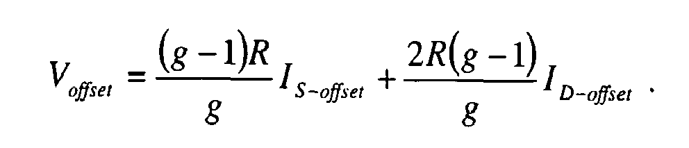
- Once a user has achieved a desired gain from the
amplifier circuit 400, the voltage offset Voffset may be adjusted to compensate for sensor offset by adjusting either, or both, of the offset currents, IS-offset 426 and ID-offset 428. - Accordingly, the
amplifier circuit 400 illustrated inFigure 4 provides a user with the ability to control thecurrent sources 402 and/or 404 to inject the offset currents IS-offset 426 and ID-offset 428 at desired current levels to create a voltage offset Voffset that offsets the sensor offset contribution to the input signal. Thecurrent sources I S-offset 428. In one example, the user may set up a sensor to generate a 'zero' signal. Thus, in setting the input offset adjustment, the user may configure a sensor to generate a signal that is selected to represent a zero level. In the case of a TCD employed with a GC, the sensor may be configured to provide a balanced signal level at the sensor output leads. That is, the sensor may be subjected to a temperature at which all of the resistor filaments should be of equal value. The user may then adjust the current source(s) 402 and/or 404 to generate anI D-offset 426 and/or IS-offset 428 that applies a Voffset at the invertinginputs negative outputs -
Figure 5 is a schematic diagram of another example of a single-ended, programmablegain amplifier circuit 500 consistent with the present invention. Theamplifier circuit 500 may include anamplifier 502, afeedback network 504, acurrent source 506, a compensatingimpedance 508, and a plurality of switches such as fourswitches feedback network 504 may include an R2R impedance ladder network formed byseries ladder impedances parallel ladder impedances amplifier 502. It is appreciated by those skilled in the art that while fourswitches 510a-d, fourseries ladder impedances 512a-d, and fourparallel impedances 512a-d are shown, this number is an example and any number of these components may be utilized without departing from the scope of this invention. Aninput signal 516 may be received viasignal input 518, which is in signal communication with anon-inverting input 520 of theamplifier 502 via the compensatingimpedance 508. Theamplifier 502 outputs an amplifiedsignal 522 at asignal output 524 of theamplifier 502 relative to signalground 526. - The plurality of
switches switch Sg3 510d may be selected to set the gain of theamplifier circuit 500 to a gain value of 3. Similarly, theswitch Sg6 510c may be selected to set the gain to a gain value of 6, theswitch Sg12 510b may be selected to set the gain to a gain value of 12, and theswitch Sg24 510a may be selected to set the gain to a gain value of 24. The gain settings are dependent on the configuration of the impedance elements in theR2R feedback network 504 for each switch setting. For example, theswitch Sg3 510d is illustrated in a closed state, leaving theimpedance element 512d as the lone feedback impedance element in signal communication with the negative input (i.e., an invertinginput 528 of the amplifier 502) and theoutput 524 of theamplifier 502. By opening theswitch Sg3 510d and closing theswitch Sg6 510c, the configuration of theR2R feedback network 504 changes to provide an increased feedback impedance relative to the impedance between thenegative input node 528 of the inverting input of theamplifier 502 andsignal ground 526. The values of the impedances may be selected such that the gain is thereby effectively doubled (i.e., to a gain value of 6). Similarly, opening theswitch Sg6 510c and closing theswitch Sg12 510b raises the gain to a gain value of 12, and opening theswitch Sg12 510b and closing theswitch Sg24 510a raises the gain to a gain value of 24. - The
current source 506 may be adjusted to control the input offset at the negative amplifier input (i.e., the inverting input 528) of theamplifier 502. In this example, the negative input node impedance of thefeedback network 504 as seen at the invertinginput 528 does not change when a different gain is selected. In this example, the impedance values may be selected as follows: theseries ladder impedances parallel ladder impedance 514a may each be set of an impedance value of R, where R is a resistance value; and theparallel ladder impedances series ladder impedance 512d may each be set to an impedance value of 2R. Given the impedance values indicated in this example, the voltage offset Voffset at the invertinginput 528 of theamplifier 502 may be determined according to:
- The user may set the voltage offset Voffset to compensate for a determined sensor offset by adjusting the offset current Ioffset generated by the
current source 506. - The
amplifier circuit 500 illustrated inFigure 5 provides a user with the ability to control thecurrent source 506 to inject the offset current Ioffset to create a voltage offset Voffset that offsets the sensor offset contribution to theinput signal 516. The gain may also be programmed using theswitches feedback network 504 as seen at the invertinginput 528 of theamplifier circuit 500, thereby eliminating the effect that changing the gain would otherwise have on the input offset adjustment. -
Figure 6 is a schematic diagram of another example of a differential instrumentation, programmablegain amplifier circuit 600 consistent with the present invention. Theamplifier circuit 600 may include first and secondcurrent sources feedback network 606, afirst amplifier 608, asecond amplifier 610, a first compensatingimpedance 612, a second compensatingimpedance 614, a first plurality of switches such as fourswitches switches first amplifier 608 andsecond amplifier 610 are differential amplifiers such as, for example, op-amps. The first compensatingimpedance 614 is in signal communication with anon-inverting input 620 of thefirst amplifier 608 and the second compensatingimpedance 614 is in signal communication with anon-inverting input 622 of thesecond amplifier 610. The firstcurrent source 602 is in signal communication with an invertinginput 624 of thefirst amplifier 608. The secondcurrent source 604 is signal communication with both the invertinginput 624 of thefirst amplifier 608 and an invertinginput 626 of thesecond amplifier 610. The firstcurrent source 602 is also in signal communication with asignal ground 627. In operation, the first and secondcurrent sources input 624 of thefirst amplifier 608. - The
feedback network 606 may include an R2R impedance ladder network formed by first (i.e., "upper")series ladder impedances series ladder impedances parallel ladder impedances amplifiers first switches 616a-d, foursecond switches 618a-d, four firstseries ladder impedances 632a-d, four secondseries ladder impedances 634a-d and fourparallel impedances 636a-d are shown, this number is an example and any number of these components may be utilized without departing from the scope of this invention. - A
first input signal 638 may be received via a signal input 640 (e.g., the positive signal input), which is in signal communication with thenon-inverting input 620 of thefirst amplifier 608 via the first compensatingimpedance 612. Thefirst amplifier 608 outputs a first amplifiedsignal 642 at asignal output 644 of thefirst amplifier 608 relative to signalground 627. Similarly, asecond input signal 642 may be received via a signal input 644 (e.g., the negative signal input), which is in signal communication with thenon-inverting input 622 of thesecond amplifier 610 via the second compensatingimpedance 614. Thesecond amplifier 610 outputs a second amplifiedsignal 646 at asignal output 648 of thesecond amplifier 610 relative to signalground 627. As an example, a sensor may be put in signal communication with the differential positive andnegative signal inputs - The inverting
amplifier input 624 of thefirst amplifier 608 is in signal communication with thefeedback network 606 via the first switch-bank 616a-d at a first node that corresponds to the invertinginput 624 to thefirst amplifier 608. The invertingamplifier input 626 of thesecond amplifier 610 is in signal communication with thefeedback network 606 via the second switch-bank 618a-d at a second node that corresponds to the invertinginput 626 to thesecond amplifier 610. The R2R impedance ladder network within thefeedback network 606 is formed by theparallel ladder impedances 636a-d, upperseries ladder impedances 632a-d, and lowerseries ladder impedances 634a-d. - The settings of the first and second switch-
banks 616a-d and 618a-d switch the configuration of the impedances in thefeedback network 606 to adjust the impedance values to obtain a desired gain. For example, theswitch Sg3 616d in the first switch-bank 616a-d and theswitch Sg3 618d in the second switch-bank 618a-d may be selected to set the gain of theamplifier circuit 600 to a gain value of 3. Similarly, theswitches Sg6 bank 616a-d and 618a-d may be selected to set the gain to gain value of 6, the switches Sg12 616b and 618b in each switch-bank 616a-d and 618a-d may be selected to set the gain to gain value of 12, and theswitches Sg24 bank 616a-d and 618a-d may be selected to set the gain to a gain value of 24. In these examples, the gains are dependent on the impedance of the R2R impedance ladder network, within thefeedback network 606, corresponding to the switch or switches that are closed. - As an example of operation, the first
current source 602 injects a current, IS-offset 628, at the first node corresponding to the invertinginput 624 of thefirst amplifier 608. The current, IS-offset 628, generates a voltage offset at the invertinginput 624 relative to signalground 627. The secondcurrent source 604 injects a current, ID-offset 630 into the R2R impedance ladder network to create a constant voltage drop across the R2R impedance ladder network between nodes corresponding to the invertinginput 624 offirst amplifier 608 and the invertinginput 626 of thesecond amplifier 610. The first and secondcurrent sources signal inputs upper series impedances lower impedances upper series impedance 632d andlower series impedance 634d have individual impedance values set to a resistance value of 2R;parallel impedances parallel impedance 636a has an impedance value set to a resistance value of 2R. Given the impedance values indicated in this example, the voltage offset Voffset may be determined by: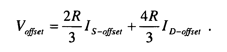
- The
amplifier circuit 600 illustrated inFigure 6 provides a user with the ability to control thecurrent sources 602 and/or 604 to inject the offset current to create a voltage offset Voffset that offsets the sensor offset contribution to the input signal. The gain may also be programmed using theswitches feedback network 606 at the invertinginputs second amplifiers amplifier circuit 600, thereby eliminating the effect that changing the gain would otherwise have on the input offset adjustment. -
Figure 7 is a schematic diagram of another example of a single-ended, programmablegain amplifier circuit 700 consistent with the present invention. Theamplifier circuit 700 receives aninput signal 702 at asignal input 704, which is in signal communication with anon-inverting input 706 of anamplifier 708 via a compensatingimpedance 710. Theamplifier circuit 700 may include afeedback network 712 that has an R2R feedback network forming a voltage divider. Thefeedback network 712 may include a firstfeedback impedance network 714 and a secondfeedback impedance network 716. The firstfeedback impedance network 714 may include series-connectedimpedances switches Sg10 720a andSg100 720b is capable of adjusting the impedance of the firstfeedback impedance network 714 by switching in/out the series-connectedimpedances feedback impedance network 716 includes parallel-connected impedances switches Sg1000 724a and Sg100,000 724b is capable of adjusting the impedance of the secondfeedback impedance network 716 by switching in/out the parallel-connected impedances Sg10 720a sets the gain of the single-ended programmablegain amplifier circuit 700 to a gain value of 10 when it is closed. Likewise, switchSg100 720b sets the gain to a gain value of 100, switchSg1000 724a sets the gain to a gain value of 1000, and switch Sg100,000 724b sets the gain to a gain value of 100,000. The gain at each switch setting is determined by the impedance at each branch (i.e., the firstfeedback impedance network 714 and the second feedback impedance network 716) of the voltage divider formed by the R2R feedback network of thefeedback network 712. - In this example, the
amplifier circuit 700 has the property that the impedance of the negative input node corresponding to an invertinginput 726 of theamplifier element 708 is constant regardless of the gain selected. As an example, the impedance values of the impedances may be selected as follows: theimpedance 718a has a resistance value of 9R, theimpedance 718b has a resistance value of 81R, theimpedance 718c has a resistance value of 810R, theimpedance 722a has a resistance value of 100R, theimpedance 722b has a resistance value of 10R, theimpedance 722c has a resistance value of R, and the compensatingimpedance 710 has a resistance value of
input 726, of theamplifier 708, is
current source 728 injects a constant offset current, Ioffset 730 intonode 726 to generate a constant offset voltage Voffset. Based on the impedance values of this example, the voltage offset Voffset may be obtained utilizing the following relationship:
- The
amplifier circuit 700 illustrated inFigure 7 provides a user with the ability to control thecurrent source 728 to inject the offset current Ioffset to create a voltage offset Voffset that offsets the sensor offset contribution to theinput signal 702. The gain may also be programmed using theswitches amplifier circuit 700, thereby eliminating the effect that changing the gain would otherwise have on the input offset adjustment. -
Figure 8 is a schematic diagram of another example of a differential instrumentation programmablegain amplifier circuit 800 consistent with the present invention. Theamplifier circuit 800 may include afeedback network 802 with switch-selectable impedance levels for both the gain impedance and the feedback impedance. A sensor may be in signal communication with the differential positive andnegative inputs positive signal input 804 is in signal communication with thenon-inverting amplifier input 808 of afirst amplifier 810 via a first compensatingimpedance 812. Thenegative signal input 806 is in signal communication with thenon-inverting amplifier input 814 of asecond amplifier 816 via a second compensatingimpedance 818. Thefirst amplifier 810 outputs a first amplifiedsignal 850 at asignal output 852 of thefirst amplifier 810. Thesecond amplifier 816 outputs a second amplifiedsignal 860 at asignal output 862 of thesecond amplifier 816. - An inverting
amplifier input 820 of thefirst amplifier 810 is in signal communication with again impedance network 822 and to a firstfeedback impedance network 824. The firstfeedback impedance network 824 forms a branch of series-connectedfeedback impedances switches gain impedance network 822 forms a branch of parallel-connectedgain impedances nodes second amplifiers Node 820 is in signal communication with the firstfeedback impedance network 824 andnode 832 is in signal communication with a secondfeedback impedance network 834. The secondfeedback impedance network 834 may form a branch of series-connectedfeedback impedances switches impedances 830a-c of thegain impedance network 822 are in signal communication with a third switch bank ofswitches switches Sg10 Sg100 Sg1000 840a, or Sg100,000 840b. SwitchesSg10 Sg100 feedback impedance networks impedances 826a-c and 836a-c in each branch to connect with theimpedance 830c in thegain impedance network 822. SwitchesSg1000 840a and Sg100,000 840b of the third switch-bank adjust the impedance of thegain impedance network 822 by switching in/out the parallel-connected impedances 830a-c to connect with the impedances of the first and secondfeedback impedance networks - A first
current source 842 injects acurrent I S-offset 844 atnode 820 at the inverting input of thefirst amplifier 810. Thecurrent I S-offset 844 generates a voltage offset relative to signalground 846 at thenode 820. A secondcurrent source 848 injects acurrent I D-offset 850 into thegain impedance network 822 to create a constant voltage drop across thegain impedance network 822 betweennodes current sources signal inputs impedances impedances impedances impedance 830a is set to a resistance value of 200R, theimpedance 830b is set to a resistance value of 20R, and theimpedance 830c is set to a resistance value of 2R. Given these values, the voltage offset, Voffset , may be determined by:
- The
amplifier circuit 800 illustrated inFigure 8 provides a user with the ability to control thecurrent sources 842 and/or 848 to inject the offset current to create a voltage offset Voffset that offsets the sensor offset contribution to the input signal. The gain may also be programmed using theswitches 828a-b, 838a-b and 840a-b in a manner that does not change the impedance at the differential input (i.e., the input impedances of thefeedback network 802 at the invertinginputs second amplifiers amplifier circuit 800, thereby eliminating the effect that changing the gain would otherwise have on the input offset adjustment. - The examples of amplifier circuits described with reference to
Figures 3-8 allow a user to set an input offset to compensate for a sensor offset. For the single-ended amplifier circuits such as theamplifier circuits Figures 3 ,5 , and7 , a TCD in a bridge circuit may have one lead from the bridge circuit in signal communication with the single-ended input and the other lead grounded. In a GC application, the single-ended amplifier circuit may be configured and set to operate in the presence of the reference gas only. The input offset may be adjusted by adjusting the current source in the single-ended amplifier circuit until the output of the single-ended amplifier circuit is zero. Consequently, in the presence of a sample gas, the entire output gain range is available during operation. - Similarly, for the differential instrumentation amplifier circuits such as the
amplifier circuits Figures 4 ,6 and8 , the leads of the bridge circuit of the TCD may be in signal communication with the differential inputs of the differential instrumentation amplifier circuits. The input offset may then be adjusted by adjusting the current(s) generated by the current source(s) in the differential instrumentation amplifier circuits with the TCD in the presence of a reference gas. - The programmable gain amplifier circuits such as the
amplifier circuits Figures 5 ,6 ,7 and8 enable the user to easily program the gain. The gain may be programmed by setting switches as described above or other suitable gain-adjusting devices or means. The switches may be implemented using any type of switch (e.g. a set of dipswitches, or electronic switches that may be controlled by software). Equal node impedances are provided for all gains, such that the required input offset adjustment is equal for all gains of the amplifier circuit. - One or more implementations may be configured such that the input offset adjustment is proportional to the bi-directional (positive or negative) offset input current. For a bridge circuit, a ratio-metric input offset adjustment can be realized by driving the offset adjustment current from a digital to analog converter with the bridge excitation as a reference.
- It will be understood that various aspects or details of the invention may be changed without departing from the scope of the invention. For example, the impedance networks described by example above may be implemented using a variety of topographies that provide a constant impedance at the negative input of the amplifier elements regardless of the overall gain selected for the circuit. Moreover, specific impedances, gain settings, resistances, current and voltage offsets, and other values have been provided for purposes of illustration and example and thus are not limiting. Furthermore, the foregoing description is for the purpose of illustration only, and not for the purpose of limitation-the invention being defined by the claims.
Claims (20)
- An amplifier circuit (300, 400, 500, 600, 700, 800), comprising:an amplifier (306; 408, 410; 502; 608, 610; 708; 810, 816), having a non-inverting input (320; 416, 418; 520; 620, 622; 706; 808, 814), an inverting input (318; 422, 424; 528; 624, 626; 726; 820, 832), and an amplifier output (322; 440, 442; 524; 644, 646; 852, 862);a feedback network (308, 406, 504, 606, 712, 802) in signal communication with the amplifier output (322; 440, 442; 524; 644, 646; 852, 862) and the inverting input (318; 422, 424; 528; 624, 626; 726; 820, 832); andat least one current source (310; 402, 404; 506; 602, 604; 728; 842, 848) in signal communication with the inverting input (318; 422, 424; 528; 624, 626; 726; 820, 832), the one or at least one of the current sources being adjustable to a plurality of selectable input offsets to generate a plurality of corresponding voltage offsets at the inverting input.
- The amplifier circuit of claim 1, wherein the feedback network (308, 406, 504, 606, 712, 802) includes a first feedback impedance element (314; 444, 446; 512a-d; 632a-d, 634a-d; 718a-c; 826a-c, 836a-c) in signal communication with the amplifier output and the inverting input, and a second feedback impedance element (316; 448; 514a-d; 636a-d; 722a-b; 830a-c) in signal communication with the inverting input.
- The amplifier circuit of claim 2, wherein the first feedback impedance element (314; 444, 446; 512a-d; 632a-d, 634a-d; 718a-c; 826a-c, 836a-c) has an impedance value dependent on the gain of the amplifier.
- The amplifier circuit of claim 1, 2 or 3, wherein the feedback network (504, 606, 712, 802) is adjustable to a plurality of gain settings of the amplifier circuit, and the feedback network is configured such that an impedance of the feedback network at the inverting input (528; 624, 626; 726; 820, 832) is equal for all gain settings, whereby in particular the plurality of selectable input offsets and the plurality of corresponding voltage offsets are independent of the plurality of gain settings.
- The amplifier circuit of claim 1, 2 or 3, wherein:the feedback network (504, 606, 712, 802) includes a plurality of impedance elements in signal communication with the inverting input (528; 624, 626; 726; 820, 832), and a plurality of switches (510a-d; 616a-d, 618a-d; 720a-b, 722a-b; 828a-b, 838a-b, 840a-b) adjustable to a plurality of gain settings of the amplifier circuit; andthe feedback network is configured such that the impedance of the feedback network at the inverting input (528; 624, 626; 726; 820, 832) is equal for all gain settings, whereby in particular the plurality of selectable input offsets and the plurality of corresponding voltage offsets are independent of the plurality of gain settings.
- The amplifier circuit of claim 5, wherein the plurality of impedance elements includes a plurality of series-connected impedance elements (512a-d; 632a-d, 634a-d; 718a-c; 826a-c, 836a-c) in signal communication with the inverting input (528; 624, 626; 726; 820, 832) and the amplifier output (528; 624, 626; 726; 820, 832), and a plurality of parallel-connected impedance elements (514a-d; 636a-d; 722a-b; 830a-c) in signal communication with the inverting input.
- The amplifier circuit of claim 1, wherein:the amplifier is a first amplifier (408; 608; 810), the non-inverting input is a first non-inverting input, the inverting input is a first inverting input, and the amplifier output is a first amplifier output;the amplifier circuit further includes a second amplifier (410; 610; 816) having a second non-inverting input, a second inverting input, and a second amplifier output; andthe feedback network (406, 606, 802) is in signal communication with the second amplifier output and the second inverting input, in addition to the first amplifier output and the first inverting input.
- The amplifier circuit of claim 7, wherein:the current source includes a first current source (402; 602; 842) in signal communication with the first inverting input (422; 624; 820), and a second current source (404; 604; 848) in signal communication with the first inverting input (408; 608; 810) and with the second inverting input (424; 626; 832); andat least one of the first and second current sources (402, 404; 602, 604; 842, 848) is adjustable to the plurality of selectable input offsets to generate a plurality of corresponding voltage offsets at the first and second inverting inputs.
- The amplifier circuit of claim 7 or 8, wherein the feedback network (406, 606, 802) includes a first feedback impedance element (444; 632a-d; 826a-c) in signal communication with the first amplifier output (440; 644; 852) and the first inverting input (408; 608; 810), a second feedback impedance element (446; 634a-d; 836a-c) in signal communication with the second amplifier output (442; 646; 862) and the second inverting input (424; 626; 832), and a gain impedance element (448; 636a-d; 830a-c) in signal communication with the first inverting input and the second inverting input.
- The amplifier circuit of claim 9, wherein the first feedback impedance element (444; 632a-d; 826a-c) and the second feedback impedance element (446; 634a-d; 836a-c) each have an impedance value dependent on the gain of each of the first and second amplifiers.
- The amplifier circuit according to any of claims 7 to 10, wherein the feedback network (406, 606, 802) is adjustable to a plurality of gain settings of the amplifier circuit, and the feedback network is configured such that the impedance between the first and second inverting inputs is equal for all gain settings, whereby in particular the plurality of selectable input offsets and the plurality of corresponding voltage offsets are independent of the plurality of gain settings.
- The amplifier circuit according to any of claims 7 to 11, wherein:the feedback network (606, 802) includes a plurality of impedance elements (632a-b, 634a-b, 636a-d; 826a-b, 836a-b, 830a-c) in signal communication with the first and/or second inverting inputs (624, 626; 820, 832), and a plurality of switches (616a-d, 618a-d; 828a-b, 838a-b, 840a-b) adjustable to a plurality of gain settings of the amplifier circuit; andthe feedback network is configured such that the impedance between the first and second inverting inputs is equal for all gain settings, whereby in particular the plurality of selectable input offsets and the plurality of corresponding voltage offsets are independent of the plurality of gain settings.
- The amplifier circuit of claim 12, wherein the plurality of impedance elements includes:a plurality of first series-connected impedance elements (632a-d; 826a-c) in signal communication with the first inverting input and the first amplifier output;a plurality of second series-connected impedance elements (634a-d; 836a-c) in signal communication with the second inverting input and the second amplifier output; anda plurality of parallel-connected impedance elements (636a-d; 830a-c) in signal communication with the first and second inverting inputs.
- The amplifier circuit of any of claims 1-13, wherein at least one amplifier (306; 408, 410; 502; 608, 610; 708; 810, 816) is in signal communication with a gas detector (108).
- The amplifier circuit of any of claims 1-14, wherein at least one amplifier (306; 408, 410; 502; 608, 610; 708; 810, 816) is in signal communication with a bridge output of a bridge circuit (200), and the bridge circuit includes at least two temperature-sensitive resistive elements (208-220), one of the resistive elements communicating with a first gas source (120) and the other resistive element communicating with a second gas source (124).
- The amplifier circuit of any of claims 1-15, wherein at least one amplifier (306; 408, 410; 502; 608, 610; 708; 810, 816) is in signal communication with a gas detector (108), and the gas detector is in flow communication with a chromatographic column (104).
- A method for adjusting an input offset at an input of an amplifier circuit (300, 400, 500, 600, 700, 800), comprising:amplifying an input signal in a differential amplifier (306; 408, 410; 502; 608, 610; 708; 810, 816) to generate an output signal;feeding back the output signal through a feedback network (308, 406, 504, 606, 712, 802) to an inverting input of the differential amplifier; anddriving an adjustable current into the inverting input, the adjustable current being adjustable to a plurality of selectable input offsets to generate a plurality of corresponding voltage offsets at the inverting input.
- The method of claim 17, further including adjusting the feedback network (504, 606, 712, 802) to a selected one of a plurality of selectable gain settings of the amplifier circuit, wherein the impedance at the inverting input is equal for any gain setting selected and adjustment of the current is independent of the selected gain setting.
- The method of claim 17 or 18, further including receiving an input signal at a non-inverting input of the differential amplifier from a gas detector (108).
- The method of any of claims 17-19, wherein the input signal is indicative of a concentration of a gas flowed from a chromatographic column (104).
Priority Applications (3)
| Application Number | Priority Date | Filing Date | Title |
|---|---|---|---|
| EP07025219A EP2075910A1 (en) | 2007-12-28 | 2007-12-28 | Instrumentation amplification with input offset adjustment |
| JP2008325813A JP2009165121A (en) | 2007-12-28 | 2008-12-22 | Amplifier circuit and offset adjustment method |
| US12/342,614 US20090167432A1 (en) | 2007-12-28 | 2008-12-23 | Instrumentation amplification with input offset adjustment |
Applications Claiming Priority (1)
| Application Number | Priority Date | Filing Date | Title |
|---|---|---|---|
| EP07025219A EP2075910A1 (en) | 2007-12-28 | 2007-12-28 | Instrumentation amplification with input offset adjustment |
Publications (1)
| Publication Number | Publication Date |
|---|---|
| EP2075910A1 true EP2075910A1 (en) | 2009-07-01 |
Family
ID=39430180
Family Applications (1)
| Application Number | Title | Priority Date | Filing Date |
|---|---|---|---|
| EP07025219A Withdrawn EP2075910A1 (en) | 2007-12-28 | 2007-12-28 | Instrumentation amplification with input offset adjustment |
Country Status (3)
| Country | Link |
|---|---|
| US (1) | US20090167432A1 (en) |
| EP (1) | EP2075910A1 (en) |
| JP (1) | JP2009165121A (en) |
Cited By (3)
| Publication number | Priority date | Publication date | Assignee | Title |
|---|---|---|---|---|
| EP2852055A1 (en) * | 2013-09-20 | 2015-03-25 | Honeywell International Inc. | Programmable-gain instrumentation amplifier |
| WO2019151992A1 (en) * | 2018-01-30 | 2019-08-08 | Power Integrations, Inc. | Signal amplifier with calibrated reference |
| GB2604707A (en) * | 2020-12-30 | 2022-09-14 | Analog Devices Inc | Amplifier input offset compensation |
Families Citing this family (29)
| Publication number | Priority date | Publication date | Assignee | Title |
|---|---|---|---|---|
| KR20100129575A (en) * | 2009-06-01 | 2010-12-09 | 삼성전자주식회사 | Non-inverting amplifier and voltage supply circuit including it |
| CN102667465B (en) * | 2009-11-25 | 2014-09-17 | 西门子公司 | Method and apparatus for gas chromatographic analysis of gas samples |
| US8779796B2 (en) * | 2010-09-29 | 2014-07-15 | Taiwan Semiconductor Manufacturing Co., Ltd. | Method and apparatus for device parameter measurement |
| KR101419806B1 (en) * | 2010-11-19 | 2014-07-17 | 한국전자통신연구원 | Variable gain amplifier with fixed bandwidth |
| CN106877685B (en) | 2011-02-24 | 2019-01-01 | 克兰电子公司 | AC/DC power conversion system and its manufacturing method |
| US8890630B2 (en) | 2011-07-18 | 2014-11-18 | Crane Electronics, Inc. | Oscillator apparatus and method with wide adjustable frequency range |
| US8885308B2 (en) | 2011-07-18 | 2014-11-11 | Crane Electronics, Inc. | Input control apparatus and method with inrush current, under and over voltage handling |
| US8866551B2 (en) | 2012-09-10 | 2014-10-21 | Crane Electronics, Inc. | Impedance compensation for operational amplifiers used in variable environments |
| US9525388B1 (en) | 2013-07-03 | 2016-12-20 | Avnera Corporation | On-chip resistor divider compensation with a 2Vrms input |
| US9362874B2 (en) * | 2013-07-10 | 2016-06-07 | Fairchild Semiconductor Corporation | Differential measurements with a large common mode input voltage |
| US9831768B2 (en) | 2014-07-17 | 2017-11-28 | Crane Electronics, Inc. | Dynamic maneuvering configuration for multiple control modes in a unified servo system |
| US9041378B1 (en) | 2014-07-17 | 2015-05-26 | Crane Electronics, Inc. | Dynamic maneuvering configuration for multiple control modes in a unified servo system |
| US9230726B1 (en) | 2015-02-20 | 2016-01-05 | Crane Electronics, Inc. | Transformer-based power converters with 3D printed microchannel heat sink |
| US9160228B1 (en) | 2015-02-26 | 2015-10-13 | Crane Electronics, Inc. | Integrated tri-state electromagnetic interference filter and line conditioning module |
| US9293999B1 (en) | 2015-07-17 | 2016-03-22 | Crane Electronics, Inc. | Automatic enhanced self-driven synchronous rectification for power converters |
| US9780635B1 (en) | 2016-06-10 | 2017-10-03 | Crane Electronics, Inc. | Dynamic sharing average current mode control for active-reset and self-driven synchronous rectification for power converters |
| US9742183B1 (en) | 2016-12-09 | 2017-08-22 | Crane Electronics, Inc. | Proactively operational over-voltage protection circuit |
| US9735566B1 (en) | 2016-12-12 | 2017-08-15 | Crane Electronics, Inc. | Proactively operational over-voltage protection circuit |
| US9979285B1 (en) | 2017-10-17 | 2018-05-22 | Crane Electronics, Inc. | Radiation tolerant, analog latch peak current mode control for power converters |
| US10651797B2 (en) * | 2018-04-09 | 2020-05-12 | Infineon Technologies Austria Ag | Amplifier offset and compensation |
| CN108880547A (en) * | 2018-08-21 | 2018-11-23 | 中国船舶重工集团公司第七0四研究所 | Bridge circuit zero offset on-line correction method based on electric current injection |
| US10505403B1 (en) | 2018-08-31 | 2019-12-10 | Apple Inc. | Wireless charging system with temperature sensing |
| US10658878B2 (en) | 2018-08-31 | 2020-05-19 | Apple Inc. | Wireless charging system with temperature sensor array |
| US10425080B1 (en) | 2018-11-06 | 2019-09-24 | Crane Electronics, Inc. | Magnetic peak current mode control for radiation tolerant active driven synchronous power converters |
| US10944368B2 (en) * | 2019-02-28 | 2021-03-09 | Advanced Micro Devices, Inc. | Offset correction for pseudo differential signaling |
| EP4004604B1 (en) | 2019-07-29 | 2025-07-02 | Shenzhen Xpectvision Technology Co., Ltd. | Amplifier for dark noise compensation |
| WO2022035730A1 (en) | 2020-08-13 | 2022-02-17 | Owlet Baby Care, Inc. | Multi-channel common-mode coupled ac gain amplifier |
| US12160212B2 (en) | 2021-01-21 | 2024-12-03 | Maxim Integrated Products, Inc. | Offset voltage compensation |
| KR102827261B1 (en) * | 2022-12-23 | 2025-07-01 | (주)나노아이오닉스코리아 | Method and device for compensating hydrogen sensor offset |
Citations (8)
| Publication number | Priority date | Publication date | Assignee | Title |
|---|---|---|---|---|
| US5146788A (en) * | 1990-10-25 | 1992-09-15 | Becton, Dickinson And Company | Apparatus and method for a temperature compensation of a catheter tip pressure transducer |
| US5379630A (en) * | 1993-06-28 | 1995-01-10 | Hewlett-Packard Company | Thermal conductivity detector |
| US20050265422A1 (en) * | 2004-05-28 | 2005-12-01 | Honeywell International Inc. | Differetial thermal sensors |
| US7095275B2 (en) | 2003-06-25 | 2006-08-22 | Renesas Technology Corp. | BTL amplifier capable of providing stability of offset compensation |
| US7117714B2 (en) * | 2004-12-16 | 2006-10-10 | Oki Electric Industry Co., Ltd. | Output amplifier circuit and sensor device using the same |
| US20070115047A1 (en) | 2003-09-26 | 2007-05-24 | D Abramo Paolo | Differential amplifier arrangement |
| US20070241813A1 (en) | 2004-05-18 | 2007-10-18 | Koninklijke Philips Electronics, N.V. | Amplifier Circuit with Automatic Gain Correction |
| US7304534B2 (en) | 2005-02-18 | 2007-12-04 | Infineon Technologies Ag | Amplifier arrangement, and method for compensating for an offset |
Family Cites Families (5)
| Publication number | Priority date | Publication date | Assignee | Title |
|---|---|---|---|---|
| US4881047A (en) * | 1988-06-20 | 1989-11-14 | Waller Jr James K | Automatic gain expansion system |
| US6956439B1 (en) * | 2003-12-12 | 2005-10-18 | National Semiconductor Corporation | Transimpedance amplifier with controllable noise reduction |
| US7154331B2 (en) * | 2004-06-29 | 2006-12-26 | Intel Corporation | Adapting operational amplifier frequency response respective to closed loop gain |
| US7319220B2 (en) * | 2006-03-29 | 2008-01-15 | Mindspeed Technologies, Inc. | Trans-impedance amplifier with offset current |
| TWI418802B (en) * | 2008-07-09 | 2013-12-11 | Analog Devices Inc | Comprehensive front-end for instrumentation system |
-
2007
- 2007-12-28 EP EP07025219A patent/EP2075910A1/en not_active Withdrawn
-
2008
- 2008-12-22 JP JP2008325813A patent/JP2009165121A/en active Pending
- 2008-12-23 US US12/342,614 patent/US20090167432A1/en not_active Abandoned
Patent Citations (8)
| Publication number | Priority date | Publication date | Assignee | Title |
|---|---|---|---|---|
| US5146788A (en) * | 1990-10-25 | 1992-09-15 | Becton, Dickinson And Company | Apparatus and method for a temperature compensation of a catheter tip pressure transducer |
| US5379630A (en) * | 1993-06-28 | 1995-01-10 | Hewlett-Packard Company | Thermal conductivity detector |
| US7095275B2 (en) | 2003-06-25 | 2006-08-22 | Renesas Technology Corp. | BTL amplifier capable of providing stability of offset compensation |
| US20070115047A1 (en) | 2003-09-26 | 2007-05-24 | D Abramo Paolo | Differential amplifier arrangement |
| US20070241813A1 (en) | 2004-05-18 | 2007-10-18 | Koninklijke Philips Electronics, N.V. | Amplifier Circuit with Automatic Gain Correction |
| US20050265422A1 (en) * | 2004-05-28 | 2005-12-01 | Honeywell International Inc. | Differetial thermal sensors |
| US7117714B2 (en) * | 2004-12-16 | 2006-10-10 | Oki Electric Industry Co., Ltd. | Output amplifier circuit and sensor device using the same |
| US7304534B2 (en) | 2005-02-18 | 2007-12-04 | Infineon Technologies Ag | Amplifier arrangement, and method for compensating for an offset |
Cited By (7)
| Publication number | Priority date | Publication date | Assignee | Title |
|---|---|---|---|---|
| EP2852055A1 (en) * | 2013-09-20 | 2015-03-25 | Honeywell International Inc. | Programmable-gain instrumentation amplifier |
| US9065400B2 (en) | 2013-09-20 | 2015-06-23 | Honeywell International Inc. | Programmable-gain instrumentation amplifier |
| WO2019151992A1 (en) * | 2018-01-30 | 2019-08-08 | Power Integrations, Inc. | Signal amplifier with calibrated reference |
| US11095263B2 (en) | 2018-01-30 | 2021-08-17 | Power Integrations, Inc. | Signal amplifier with calibrated reference |
| GB2604707A (en) * | 2020-12-30 | 2022-09-14 | Analog Devices Inc | Amplifier input offset compensation |
| US11626847B2 (en) | 2020-12-30 | 2023-04-11 | Analog Devices, Inc. | Amplifier input offset compensation |
| GB2604707B (en) * | 2020-12-30 | 2024-04-17 | Analog Devices Inc | Amplifier input offset compensation |
Also Published As
| Publication number | Publication date |
|---|---|
| US20090167432A1 (en) | 2009-07-02 |
| JP2009165121A (en) | 2009-07-23 |
Similar Documents
| Publication | Publication Date | Title |
|---|---|---|
| EP2075910A1 (en) | Instrumentation amplification with input offset adjustment | |
| JP5815519B2 (en) | Wide dynamic range electrometer with fast response | |
| EP0733201B1 (en) | System for measuring properties of materials | |
| US8587330B2 (en) | Electrical resonance detection of particles and analytes in microfluidic channels | |
| US10126277B2 (en) | Method and thermal conductivity detector | |
| CN113970693A (en) | Apparatus and method for smart sensor applications | |
| US20160112037A1 (en) | Control circuit for use with a sensor, and measurement system including such a control circuit | |
| Sen et al. | An improved lead wire compensation technique for conventional four wire resistance temperature detectors (RTDs) | |
| Ahmed et al. | Integrated CMOS-MEMS flow sensor with high sensitivity and large flow range | |
| Pradhan et al. | An improved lead compensation technique for three-wire resistance temperature detectors | |
| Hijazi et al. | Time-based calibration-less read-out circuit for interfacing wide range MOX gas sensors | |
| Hu et al. | Calibration of an AC zero potential circuit for two-dimensional impedimetric sensor matrices | |
| RU2586084C1 (en) | Multi-channel converter of resistance of resistive sensors into voltage | |
| US7268711B1 (en) | Method and circuit for amplitude compensation in a digital-to-analog converter | |
| KR19980076201A (en) | Temperature measuring device using RTD | |
| WO2012053992A1 (en) | Current source with active common mode rejection | |
| JPH03503684A (en) | Improved set point control circuit for infrared gas analyzer | |
| Wani et al. | Dual-Range Multi-Mode Signal Conditioning Circuits for Resistive Sensors | |
| Munoz et al. | Generalized impedance converter as a new sensor signal conditioning circuit | |
| CZ2021146A3 (en) | Connection with current mirrors, method of impedance measurement and method of current to voltage conversion in this connection | |
| Mariscotti | A low cost capacitive bridge based on voltage drop balance | |
| CN117724378A (en) | A programmable resistor and a resistance strain gauge calibration method based on the programmable resistor | |
| Keskin | Operational Amplifiers | |
| Woodward et al. | Sensor Circuits and Digitally Controlled Potentiometers | |
| Acosta | National Monthly Product Training for January/2009 |
Legal Events
| Date | Code | Title | Description |
|---|---|---|---|
| PUAI | Public reference made under article 153(3) epc to a published international application that has entered the european phase |
Free format text: ORIGINAL CODE: 0009012 |
|
| AK | Designated contracting states |
Kind code of ref document: A1 Designated state(s): AT BE BG CH CY CZ DE DK EE ES FI FR GB GR HU IE IS IT LI LT LU LV MC MT NL PL PT RO SE SI SK TR |
|
| AX | Request for extension of the european patent |
Extension state: AL BA HR MK RS |
|
| AKX | Designation fees paid | ||
| STAA | Information on the status of an ep patent application or granted ep patent |
Free format text: STATUS: THE APPLICATION IS DEEMED TO BE WITHDRAWN |
|
| 18D | Application deemed to be withdrawn |
Effective date: 20100105 |
|
| REG | Reference to a national code |
Ref country code: DE Ref legal event code: 8566 |