EP2069776B1 - Method and apparatus for analyzing solutions - Google Patents
Method and apparatus for analyzing solutions Download PDFInfo
- Publication number
- EP2069776B1 EP2069776B1 EP07813900.3A EP07813900A EP2069776B1 EP 2069776 B1 EP2069776 B1 EP 2069776B1 EP 07813900 A EP07813900 A EP 07813900A EP 2069776 B1 EP2069776 B1 EP 2069776B1
- Authority
- EP
- European Patent Office
- Prior art keywords
- test
- test element
- light
- radiation
- aqueous solution
- Prior art date
- Legal status (The legal status is an assumption and is not a legal conclusion. Google has not performed a legal analysis and makes no representation as to the accuracy of the status listed.)
- Active
Links
- 238000000034 method Methods 0.000 title description 33
- 238000012360 testing method Methods 0.000 claims description 183
- 230000005855 radiation Effects 0.000 claims description 148
- 239000007864 aqueous solution Substances 0.000 claims description 80
- 239000000758 substrate Substances 0.000 claims description 25
- 239000000126 substance Substances 0.000 claims description 14
- 230000004044 response Effects 0.000 claims description 5
- 238000009736 wetting Methods 0.000 claims description 4
- 230000005540 biological transmission Effects 0.000 claims description 2
- 230000000875 corresponding effect Effects 0.000 description 44
- 238000001514 detection method Methods 0.000 description 40
- 230000008569 process Effects 0.000 description 28
- ZAMOUSCENKQFHK-UHFFFAOYSA-N Chlorine atom Chemical compound [Cl] ZAMOUSCENKQFHK-UHFFFAOYSA-N 0.000 description 26
- 229910052801 chlorine Inorganic materials 0.000 description 26
- 239000000460 chlorine Substances 0.000 description 26
- 239000000463 material Substances 0.000 description 17
- XLYOFNOQVPJJNP-UHFFFAOYSA-N water Substances O XLYOFNOQVPJJNP-UHFFFAOYSA-N 0.000 description 17
- 230000004913 activation Effects 0.000 description 15
- 238000001994 activation Methods 0.000 description 15
- 238000005259 measurement Methods 0.000 description 14
- 230000006870 function Effects 0.000 description 13
- 230000001276 controlling effect Effects 0.000 description 12
- WKBOTKDWSSQWDR-UHFFFAOYSA-N Bromine atom Chemical compound [Br] WKBOTKDWSSQWDR-UHFFFAOYSA-N 0.000 description 11
- GDTBXPJZTBHREO-UHFFFAOYSA-N bromine Substances BrBr GDTBXPJZTBHREO-UHFFFAOYSA-N 0.000 description 11
- 229910052794 bromium Inorganic materials 0.000 description 11
- 239000008280 blood Substances 0.000 description 9
- 210000004369 blood Anatomy 0.000 description 9
- 230000008859 change Effects 0.000 description 9
- 239000012491 analyte Substances 0.000 description 7
- 239000000243 solution Substances 0.000 description 7
- 239000010432 diamond Substances 0.000 description 6
- 238000004519 manufacturing process Methods 0.000 description 6
- 239000003086 colorant Substances 0.000 description 5
- 239000000203 mixture Substances 0.000 description 5
- 230000003287 optical effect Effects 0.000 description 5
- 238000012545 processing Methods 0.000 description 4
- 238000009826 distribution Methods 0.000 description 3
- 230000000694 effects Effects 0.000 description 3
- 238000002834 transmittance Methods 0.000 description 3
- 0 *CCC1C*CC1 Chemical compound *CCC1C*CC1 0.000 description 2
- QGZKDVFQNNGYKY-UHFFFAOYSA-N Ammonia Chemical compound N QGZKDVFQNNGYKY-UHFFFAOYSA-N 0.000 description 2
- WQZGKKKJIJFFOK-GASJEMHNSA-N Glucose Natural products OC[C@H]1OC(O)[C@H](O)[C@@H](O)[C@@H]1O WQZGKKKJIJFFOK-GASJEMHNSA-N 0.000 description 2
- KFSLWBXXFJQRDL-UHFFFAOYSA-N Peracetic acid Chemical compound CC(=O)OO KFSLWBXXFJQRDL-UHFFFAOYSA-N 0.000 description 2
- 230000009471 action Effects 0.000 description 2
- 238000004458 analytical method Methods 0.000 description 2
- 238000006243 chemical reaction Methods 0.000 description 2
- 238000004587 chromatography analysis Methods 0.000 description 2
- 239000011248 coating agent Substances 0.000 description 2
- 238000000576 coating method Methods 0.000 description 2
- 230000002596 correlated effect Effects 0.000 description 2
- 230000009849 deactivation Effects 0.000 description 2
- 238000010586 diagram Methods 0.000 description 2
- 239000008103 glucose Substances 0.000 description 2
- 238000005534 hematocrit Methods 0.000 description 2
- 230000001105 regulatory effect Effects 0.000 description 2
- 239000004065 semiconductor Substances 0.000 description 2
- 238000001228 spectrum Methods 0.000 description 2
- 230000008961 swelling Effects 0.000 description 2
- 210000002700 urine Anatomy 0.000 description 2
- QDHHCQZDFGDHMP-UHFFFAOYSA-N Chloramine Chemical compound ClN QDHHCQZDFGDHMP-UHFFFAOYSA-N 0.000 description 1
- 229920004142 LEXAN™ Polymers 0.000 description 1
- 229910002651 NO3 Inorganic materials 0.000 description 1
- NHNBFGGVMKEFGY-UHFFFAOYSA-N Nitrate Chemical compound [O-][N+]([O-])=O NHNBFGGVMKEFGY-UHFFFAOYSA-N 0.000 description 1
- IOVCWXUNBOPUCH-UHFFFAOYSA-M Nitrite anion Chemical compound [O-]N=O IOVCWXUNBOPUCH-UHFFFAOYSA-M 0.000 description 1
- 239000004677 Nylon Substances 0.000 description 1
- 239000004793 Polystyrene Substances 0.000 description 1
- 229910021529 ammonia Inorganic materials 0.000 description 1
- 239000006117 anti-reflective coating Substances 0.000 description 1
- 230000003667 anti-reflective effect Effects 0.000 description 1
- 230000004888 barrier function Effects 0.000 description 1
- 230000008901 benefit Effects 0.000 description 1
- 230000000903 blocking effect Effects 0.000 description 1
- 239000003054 catalyst Substances 0.000 description 1
- 239000003153 chemical reaction reagent Substances 0.000 description 1
- 238000004891 communication Methods 0.000 description 1
- 238000004590 computer program Methods 0.000 description 1
- 239000000470 constituent Substances 0.000 description 1
- 238000012937 correction Methods 0.000 description 1
- 238000005286 illumination Methods 0.000 description 1
- 239000004973 liquid crystal related substance Substances 0.000 description 1
- 238000012986 modification Methods 0.000 description 1
- 230000004048 modification Effects 0.000 description 1
- 239000002991 molded plastic Substances 0.000 description 1
- 238000012544 monitoring process Methods 0.000 description 1
- 230000007935 neutral effect Effects 0.000 description 1
- 229920001778 nylon Polymers 0.000 description 1
- 239000004431 polycarbonate resin Substances 0.000 description 1
- 229920005668 polycarbonate resin Polymers 0.000 description 1
- 229920002223 polystyrene Polymers 0.000 description 1
- 230000001737 promoting effect Effects 0.000 description 1
- 230000001681 protective effect Effects 0.000 description 1
- 238000002310 reflectometry Methods 0.000 description 1
- 238000001429 visible spectrum Methods 0.000 description 1
- 238000003466 welding Methods 0.000 description 1
Images


Classifications
-
- G—PHYSICS
- G01—MEASURING; TESTING
- G01N—INVESTIGATING OR ANALYSING MATERIALS BY DETERMINING THEIR CHEMICAL OR PHYSICAL PROPERTIES
- G01N21/00—Investigating or analysing materials by the use of optical means, i.e. using sub-millimetre waves, infrared, visible or ultraviolet light
- G01N21/75—Systems in which material is subjected to a chemical reaction, the progress or the result of the reaction being investigated
- G01N21/77—Systems in which material is subjected to a chemical reaction, the progress or the result of the reaction being investigated by observing the effect on a chemical indicator
- G01N21/78—Systems in which material is subjected to a chemical reaction, the progress or the result of the reaction being investigated by observing the effect on a chemical indicator producing a change of colour
-
- G—PHYSICS
- G01—MEASURING; TESTING
- G01N—INVESTIGATING OR ANALYSING MATERIALS BY DETERMINING THEIR CHEMICAL OR PHYSICAL PROPERTIES
- G01N21/00—Investigating or analysing materials by the use of optical means, i.e. using sub-millimetre waves, infrared, visible or ultraviolet light
- G01N21/01—Arrangements or apparatus for facilitating the optical investigation
-
- G—PHYSICS
- G01—MEASURING; TESTING
- G01N—INVESTIGATING OR ANALYSING MATERIALS BY DETERMINING THEIR CHEMICAL OR PHYSICAL PROPERTIES
- G01N21/00—Investigating or analysing materials by the use of optical means, i.e. using sub-millimetre waves, infrared, visible or ultraviolet light
- G01N21/84—Systems specially adapted for particular applications
- G01N21/8483—Investigating reagent band
-
- G—PHYSICS
- G01—MEASURING; TESTING
- G01N—INVESTIGATING OR ANALYSING MATERIALS BY DETERMINING THEIR CHEMICAL OR PHYSICAL PROPERTIES
- G01N31/00—Investigating or analysing non-biological materials by the use of the chemical methods specified in the subgroup; Apparatus specially adapted for such methods
- G01N31/22—Investigating or analysing non-biological materials by the use of the chemical methods specified in the subgroup; Apparatus specially adapted for such methods using chemical indicators
-
- G—PHYSICS
- G01—MEASURING; TESTING
- G01N—INVESTIGATING OR ANALYSING MATERIALS BY DETERMINING THEIR CHEMICAL OR PHYSICAL PROPERTIES
- G01N33/00—Investigating or analysing materials by specific methods not covered by groups G01N1/00 - G01N31/00
- G01N33/18—Water
-
- G—PHYSICS
- G01—MEASURING; TESTING
- G01N—INVESTIGATING OR ANALYSING MATERIALS BY DETERMINING THEIR CHEMICAL OR PHYSICAL PROPERTIES
- G01N21/00—Investigating or analysing materials by the use of optical means, i.e. using sub-millimetre waves, infrared, visible or ultraviolet light
- G01N21/75—Systems in which material is subjected to a chemical reaction, the progress or the result of the reaction being investigated
- G01N21/77—Systems in which material is subjected to a chemical reaction, the progress or the result of the reaction being investigated by observing the effect on a chemical indicator
-
- Y—GENERAL TAGGING OF NEW TECHNOLOGICAL DEVELOPMENTS; GENERAL TAGGING OF CROSS-SECTIONAL TECHNOLOGIES SPANNING OVER SEVERAL SECTIONS OF THE IPC; TECHNICAL SUBJECTS COVERED BY FORMER USPC CROSS-REFERENCE ART COLLECTIONS [XRACs] AND DIGESTS
- Y10—TECHNICAL SUBJECTS COVERED BY FORMER USPC
- Y10T—TECHNICAL SUBJECTS COVERED BY FORMER US CLASSIFICATION
- Y10T436/00—Chemistry: analytical and immunological testing
- Y10T436/14—Heterocyclic carbon compound [i.e., O, S, N, Se, Te, as only ring hetero atom]
- Y10T436/142222—Hetero-O [e.g., ascorbic acid, etc.]
- Y10T436/143333—Saccharide [e.g., DNA, etc.]
- Y10T436/144444—Glucose
-
- Y—GENERAL TAGGING OF NEW TECHNOLOGICAL DEVELOPMENTS; GENERAL TAGGING OF CROSS-SECTIONAL TECHNOLOGIES SPANNING OVER SEVERAL SECTIONS OF THE IPC; TECHNICAL SUBJECTS COVERED BY FORMER USPC CROSS-REFERENCE ART COLLECTIONS [XRACs] AND DIGESTS
- Y10—TECHNICAL SUBJECTS COVERED BY FORMER USPC
- Y10T—TECHNICAL SUBJECTS COVERED BY FORMER US CLASSIFICATION
- Y10T436/00—Chemistry: analytical and immunological testing
- Y10T436/25—Chemistry: analytical and immunological testing including sample preparation
- Y10T436/2575—Volumetric liquid transfer
Definitions
- the present invention relates generally to analyzing solutions to determine concentrations of constituent solutes, and more specifically to a method and apparatus for determining one or more characteristics of an aqueous solution, and in one embodiment to a portable, hand-held, self-calibrating electronic device and associated test element for determining chemical characteristics of pool or spa water.
- test elements for analyzing aqueous solutions typically include three chemically treated pads arranged on a substrate; one for measuring free chlorine or bromine concentration, one for measuring pH level and one for measuring total alkalinity of the pool or spa water.
- a test element is typically exposed to the pool or spa water, and a chemical reaction then takes place between the chemicals on each of the pads and the pool or spa water. This causes each of the pads to change to a color that is indicative of the corresponding pool or spa water characteristic.
- the colors of the pads are then typically compared visually to a color chart that maps pad color to a corresponding pool or spa water characteristic.
- Test elements are also known for analyzing blood and urine samples.
- United States patent 5,304,468 describes a test strip and apparatus for determining blood glucose levels by measuring the reflectance of the test strip. The test strip is placed in a detector and a removable cover is then closed to shield the assembly from ambient light. The test strip is illuminated by an LED and the reflectance is measured and correlated to a blood glucose level. The device is calibrated for variations in LED brightness by placing the test into the device prior to it being wetted with blood, and adjusting power to the LED if the reflectance is different than a predetermined value. Because the red color of blood can interfere with the accuracy of the measurement, measurements are taken at two wavelengths in order to permit a first order subtraction of the background color of the blood.
- two wavelength readings permit a second order correction to eliminate chromatography effects resulting from variations in the hematocrit levels among various blood samples.
- Such devices are inconvenient to use and may be prone to inaccurate results if the cover becomes inoperative or if the user elects not to take the time to perform the pre-wetting calibration step.
- United States patent 6,979,571 describes another test strip reader wherein a protective shroud is used to separate the test strip from the optics of the device.
- the shroud is provided with a hood, camming members and fingers for guiding the test strip into a groove formed in the shroud to align the test strip with the device optics.
- Such devices are expensive to manufacture, inconvenient to use, and vulnerable to mechanical failure due to the precision location necessary for the fingers and camming members.
- the electronic device 10 includes a housing 12 defining a test element receiving port 14 configured to receive a test element 16 that has been exposed to an aqueous solution.
- the housing 12 defines an opening 36 that is sized to expose an electronic display unit 18 that forms part of the electrical circuitry carried by the housing 12.
- a switch pad or switch member 20 is positioned on one side of the housing 12, and a number of switches 22, 24 and 26 extend from the housing 12 through the switch pad or member 20.
- the housing 12 may be formed from a conventional molded plastic material, although other materials and/or material compositions are contemplated.
- FIG. 1B a cross-sectional view of the test element 16 of FIG. 1A , as viewed along section lines 1B-1B, is shown.
- the test element 16 is formed of a flexible substrate 28 having a number of pads attached thereto.
- three such pads 30, 32 and 34 are attached to one side of the flexible substrate 28, although more or fewer such pads may alternatively be attached to the substrate 28.
- Each of the pads 30, 32 and 34 is chemically treated in a conventional manner and with respective chemical reagent such that each of the pads 30, 32 and 34 react with an aqueous solution when exposed thereto and change to a color that is indicative of a corresponding characteristic of the aqueous solution.
- the test element 16 is a test strip that may be used to test the chlorine or bromine concentration, the pH level and total alkalinity of pool or spa water.
- one of the chemically treated pads, e.g., pad 30, is chemically treated such that it will change color, when exposed to an aqueous solution that is indicative of chlorine or bromine concentration of the aqueous solution.
- the pads 32 and 34 are likewise chemically treated such that one of the pads, e.g., pad 32 will change, when exposed to an aqueous solution, to a color that is indicative of a pH level of the aqueous solution, and the other pad, e.g., pad 34, will change, when exposed to the aqueous solution, to a color that is indicative of the total alkalinity of the aqueous solution.
- the test element 16 is typically exposed to the pool or spa water, and a chemical reaction then takes place between the chemicals on each of the pads 30, 32 and 34 and the pool or spa water. This causes each of the pads to change to a color that is indicative of the corresponding pool or spa water characteristic, as just described.
- the colors of the pads 30, 32 and 34 are then typically compared visually to a color chart that maps pad color to a corresponding pool or spa water characteristic.
- the color chart may, for example, be imprinted on, or attached to, a container or vessel in which the test elements are supplied.
- Typical ideal ranges for pools and spas are 1-3 ppm of chlorine (or 3-6 ppm of bromine), 80-120 ppm total alkalinity, and 7.2-7.6 pH, and in this exemplary embodiment the pads 30, 32 and 34 are chemically treated in a conventional manner and with conventional chemical compositions to provide for detection of chlorine or bromine, total alkalinity and pH in these ranges. It will be appreciated, however, that the pads may alternatively or additionally be chemically treated to provide for detection of such characteristics in other ranges.
- the pads themselves may be formed of any bibulous material, and one example of such a bibulous material that may be used to form the pads 30, 32 and 34 is, but should not be limited to, filter paper.
- the test elements 16 just described are conventionally provided with a substrate 28 that is white in color to provide a neutral background for visually comparing the colors of the pads 30, 32 and 34 to a color chart as just described.
- the test element 16 differs from such conventional test elements in that the substrate 28 is configured to control (minimize, or at least reduce) radiation reflection and transmittance during interrogation of the test pads 30, 32, 34 to facilitate analysis of the test element 16 by the electronic device 10.
- the substrate 28 may be opaque.
- opaque is used herein to include material that is effectively opaque even though it may allow the transmittance of a small amount of radiation of interest; i.e.
- the substrate 28 may be formed of a material that is sufficiently thick to be opaque, or a non-opaque material may be coated on one or both sides with an opaque coating. At least one surface 28NR of the substrate may be a non-reflective surface, either having a sufficiently dark color and/or being made of an anti-reflective material and/or having an anti-reflective coating applied to the surface 28NR.
- non-reflective means reflecting an amount of incident radiation that is no more than 10% of the amount of incident radiation that is reflected from a white (fully reflective) background in the wavelengths of interest (typically the full visible light spectrum).
- the substrate 28 is black polystyrene.
- the electronic device 10 will be described herein as being configured to determine the colors of the pads 30, 32 and 34 of the test element 16 illustrated in FIGS. 1A and 1B , and to determine and display on the display unit 18 numerical values of the corresponding chlorine (or bromine), alkalinity and pH levels of an aqueous solution to which the test element 16 has been exposed. It will be understood, however, that the test element 16 may alternatively have more or fewer such pads attached thereto, and/or be chemically treated with alternative chemical compositions configured to change color as a function of one or more different characteristics the aqueous solution.
- Examples of such alternative characteristics of the aqueous solution to which at least one pad arranged on the substrate 28 may be sensitive to include, but are not limited to, ammonia concentration, nitrite concentration, nitrate concentration, solution hardness, peracetic acid concentration, and chloramine concentration.
- the housing 12 is shown as having a top portion or cover 12A and a bottom portion 12B.
- the top portion or cover 12A defines the opening 36 through which the display unit 18 is visible and further defines a slot 14A that defines, in part, the test element receiving port 14 of FIG. 1A .
- a test element placement member 14B is configured to be attached to the underside of the top portion or cover 12A of the housing 12, and juxtaposed with the slot 14A such that a test element 16 received in the slot 14A is received on the test element placement member 14B with the bibulous material of the pads 30, 32, 34 positioned against the test element placement member 14B. Together, the slot 14A and the test element placement member 14B define the test element receiving port 14.
- the bottom portion 12B of the housing 12 is sized to receive therein a circuit board 40 having the electronic display unit 18, as well as a number of additional electrical components, mounted thereto.
- the additional electrical components include, for example, a number of conventional radiation detection circuits and a corresponding number of conventional radiation sources.
- the number of radiation sources and radiation detection circuits will correspond to the number of pads arranged on the test element 16.
- the test element 16 has three such pads 30, 32 and 34 mounted thereto
- the circuit board 40 in this embodiment accordingly has three radiation sources 42 1 -42 3 mounted thereto and three corresponding radiation detection circuits 44 1 -44 3 also mounted thereto.
- a radiation guide structure 46 defines three corresponding radiation guides members 48 1 -48 3 , wherein the radiation guide structure 46 is configured to be received on the circuit board 40 such that each radiation guide member 48 1 -48 3 is aligned with a corresponding pair of the radiation sources 42 1 -42 3 and radiation detection circuits 44 1 -44 3 , and such that the top surfaces of all of the radiation guide members 48 1 -48 3 are juxtaposed with a bottom surface of the test element placement member 14B when the top portion or cover 12A engages the bottom portion 12B.
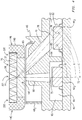
- FIG. 3 an assembled view of the bottom portion 12B of the housing 12 is shown with the circuit board 40 mounted thereto and with the radiation guide structure 46 positioned over the radiation sources 42 1 -42 3 and radiation detection circuits 44 1 -44 3 .
- the test element placement member 14B is shown in FIG. 3 as being juxtaposed over the radiation guide structure 46 as it would be when the top portion or cover 12A of the housing 12 is mounted to the bottom portion 12B.
- a test element 16 is superimposed onto FIG. 3 to illustrate that when the test element 16 is received on the test element placement member 14B with the illustrated and predefined orientation, the pads 30, 32 and 34 arranged on the test element 16 are juxtaposed over corresponding ones of the radiation guide members 48 1 -48 3 .
- Radiation emitted by the radiation sources 42 1 -42 3 is guided by corresponding ones of the radiation guide members 48 1 -48 3 to direct the emitted radiation to corresponding ones of the pads 30, 32 and 34 of the test element 16, and to also direct the resulting radiation reflected by each of the pads 30, 32 and 34 to corresponding ones of the radiation detection circuits 44 1 -44 3 .
- Signals produced by the radiation detection circuits 44 1 -44 3 in response to the reflected radiation are then used to determine the different colors of the pads 30, 32 and 34 that result from exposure of the test element 16 to an aqueous solution, as will b described in greater detail hereinafter.
- FIG. 4 a cross-section of the radiation guide structure 46, the test element placement member 14B and the test element 16 is shown as viewed along section lines 4-4 of FIG. 3 .
- the radiation source 42 2 and the radiation detection circuit 44 2 are shown as being mounted to the circuit board 40.
- the radiation guide member 48 2 defines a first cavity 60 and a second cavity 62 with a wall 64 defined between the two cavities 60 and 62.
- the cavities 60 and 62 are sized to receive the radiation source 42 2 and the radiation detection circuit 44 2 respectively therein when the radiation guide structure 46 is positioned on the circuit board 40 as illustrated in FIGS. 2 and 3 .
- the wall 64 separates the cavities 60 and 62 to minimize radiation transmission therebetween.
- An outer wall 65 surrounds and encloses the cavities 60 and 62 to define the radiation guide member 48 2 .
- the radiation guide member 48 2 defines a radiation guide in the form of a passageway 68 that extends between the cavity 60 and a top portion 66 of the radiation guide member 48 2 .
- the passageway 68 is an open passageway having one end open to the cavity 60 and an opposite end defining an opening in the top portion 66 of the radiation guide member 48 2 .
- the radiation guide member 48 2 defines another radiation guide 70 therethrough in the form of another passageway extending between the top portion 66 of the radiation guide member 48 2 and the cavity 62.
- the passageway 70 is an open passageway having one end open to the cavity 62 and an opposite end defining an opening in the top portion 66 of the radiation guide member 48 2 .
- the radiation guides 68 and 70 are circular in cross-section, although other cross-sectional shapes of the radiation guides 68 and 70 are contemplated.
- the radiation guide 68 defines a longitudinal axis 72 extending centrally therethrough.
- the longitudinal axis 72 defined by the radiation guide 68 extends through approximately a central portion of the radiation source 42 2 and also through approximately a central portion of the test element placement member 14B at a location corresponding to a center point 74 of the pad 32 of a test element 16 when the test element 16 is received on the test element placement member 14B with the predefined orientation relative to the test element placement member 14B.
- the radiation guide 70 similarly defines a longitudinal axis 76 extending centrally therethrough.
- the longitudinal axis 76 defined by the radiation guide 70 extends through approximately a central portion of the radiation detection circuit 44 2 and also through the test element placement member 14B at a location such that the longitudinal axis 76 bisects the axis 72 at approximately the center point 74 of the pad 32 of the test element 16. It will be appreciated that the radiation guides 68 and 70 may be alternatively positioned relative to the test element placement member 14B, or vice versa, such that the bisection point of the longitudinal axes 72 and 76 is positioned at any desired location of the pad 32.
- either or both of the radiation guides 68 and 70 may be alternatively positioned relative to the cavities 60 and 62 respectively such that the axis 72 extends non-centrally through the radiation source 42 2 and/or that the axis 76 extends non-centrally through the radiation detection circuit 44 2 .
- the side wall of the radiation guide 70 defines boundary axes 80 and 82 extending from the bisection point of the axes 72 and 76 to opposing locations of the side wall at the opening of the radiation guide 70 adjacent to the cavity 62, as illustrated in FIG. 4 .
- the longitudinal axes 72 and 76 define an angle, A, therebetween, the longitudinal axis 72 and the boundary axis 80 of the radiation guide 70 define another angle, B, therebetween, and the longitudinal axis 72 and the other boundary axis 82 of the radiation guide 70 define yet another angle, C, therebetween.
- the angles A, B and C are typically selected such that the longitudinal axis 72 defined through the radiation guide 68 extends through a substantially central point 75 defined on the top surface of the radiation source 42 2 , the longitudinal axis 76 defined through the radiation guide 70 extends through a substantially central point 78 defined on the top surface of the radiation detection circuit 44 2 , and the boundary axes 80 and 82, extend through a top portion of the radiation detection circuit 44 2 adjacent to the sides of the radiation detection circuit 44 2 .
- radiation emitted by the radiation source 42 2 extends through the radiation guide 68 to the pad 32 of the test element 16, and is reflected from the pad 32 of the test element 16 through the radiation guide 70 and onto the top surface of the radiation detection circuit 44 2 .
- the angle, A is approximately 45°
- the angle, B is approximately 37.73°
- the angle, C is approximately 50.804°, although other angles of A, B and C are contemplated.
- the test element placement member 14B is accordingly formed of a material that is radiation transmissive, particularly in the frequency range of the radiation source 44 2 , and that is chemically inert to the aqueous solution and the test pad chemical compositions.
- the radiation guide member 48 2 is conversely formed of a material that does not transmit radiation therethrough so that the radiation may be confined by the radiation guides 68 and 70.
- the radiation guide structure 46 is formed of pigmented nylon and the test element placement member 14B is formed of polycarbonate resin such as sold under the registered trademark LEXAN® although other materials and/or material compositions are contemplated for either structure.
- any additional radiation guide members defined by the radiation guide structure 46 e.g., radiation guide members 48 1 and 48 3 , operate identically with respect to corresponding pairs of radiation sources and radiation detection circuits.
- FIG. 5 a schematic diagram is shown of one illustrative embodiment of some of the electrical circuitry 100 mounted to the circuit board 40 illustrated in FIGS. 2 and 3 .
- the electrical circuitry 100 generally manages the overall operation of the electronic device 10, including determining one or more characteristics of an aqueous solution to which a test element 16 has been exposed.
- a control circuit 102 is configured to control operation of the electronic device 10.
- the control circuit 102 has, or has access to, a memory unit 115.
- the memory unit 115 has stored therein one or more software processes that are executable by the control circuit 102 to determine one or more characteristics of an aqueous solution to which the test element 16 has been exposed, as a function of measurement signals produced by one or more corresponding radiation detection circuits.
- three such radiation detection circuits 44 1 -44 3 are shown, and in this embodiment the electronic device 10 is configured to determine three characteristics of an aqueous solution to which the test element 16 has been exposed. It will be understood, however, that the electronic device 10 may include more or fewer such radiation detection circuits and the control circuit 102 may be configured as described herein to control any such number of radiation detection circuits to determine any corresponding number of characteristics of an aqueous solution to which the test element 16 has been exposed.
- the control circuit 102 includes a VCC input receiving a regulated voltage, V2, produced at an output of a conventional voltage regulator circuit 104, and a GND terminal that is connected to a reference potential, e.g., ground potential.
- the voltage regulator circuit 104 has an input receiving a voltage, V1, produced at an output of a conventional voltage up-converter circuit 106.
- the voltage up-converter circuit 106 has an input receiving a battery voltage, V BATT produced by any number, N, of conventional batteries 108 1 -108 N , wherein N may be any positive integer.
- the number N of batteries may be provided in the form of one or more conventional dry-cell batteries that may or may not rechargeable in a conventional manner.
- the circuit 100 may include two or more conventional dry-cell batteries connected to produce a battery voltage, V BATT , of about 3.0 volts.
- the voltage up-converter circuit 106 may be, for example, a conventional step-up DC-DC converter configured to step-up the battery voltage, V BATT , of approximately 3.0 volts to an output voltage, V1, of approximately 5.0 volts.
- the voltage up-converter circuit may be a MAX1674EUA step-up DC-DC converter circuit produced by Maxim Integrated Products.
- the voltage regulator circuit 104 in this exemplary embodiment, may be, for example, a SP6201EM5-L-3.3/TR voltage regulator produced by Sipex Corporation.
- the battery voltage, V BATT is approximately 3.0 volts nominal
- the up-converter voltage V1 is approximately 5.0 volts
- the regulated voltage V2 is also about 5.0 volts, although it will be understood that the present disclosure contemplates other values of V BATT , V1 and V2 and any conventional electronic circuitry necessary to produce such voltages.
- the circuitry 100 further includes a conventional display device 18, as described hereinabove, having a number, M, of inputs that are electrically connected to a corresponding number, M, of outputs of the control circuit 102, where M may be any positive integer.
- the display device 18 is provided in the form of a conventional liquid crystal display (LCD), one example of which is a conventional 67 segment, 3-MUX LCD unit having 24 data inputs and three control inputs. It will be understood, however, that the display device 18 may be provided in the form of other conventional LCD display units or alternatively in the form of one or more other conventional display units including, but not limited to, one or more LED display units, one or more vacuum-fluorescent display units, or the like.
- the control circuit 102 further has an on/off input that is electrically connected to one terminal of the switch 22 and also to one end of a resister, R4, having an opposite end electrically connected to ground potential. Another terminal of the switch 22 is electrically connected to one end of a resister, R1, the opposite end of which is electrically connected to the potential V2. Yet another terminal of the switch is connected to ground potential.
- the control circuit 102 is response to the "on" state of the switch 22, e.g., when the ends of the resistors R1 and R4 are electrically connected together by the switch 22, to power up to an operational state and to activate at least some of the electrical components of the electrical circuitry 100.
- the control circuit is responsive to the "off' state of the switch 22, e.g., when the end of the resistor R4 is connected by the switch 22 to ground potential, to power down or enter a conventional low-power "sleep” mode, and to deactivate at least some of the electrical components of the electronic circuitry 100.
- the control circuit 102 further includes a scroll input which is electrically connected to one terminal of the switch 24 and also to one end of a resister, R5, having an opposite end that is electrically connected to ground potential. Another terminal of the switch 24 is electrically connected to one end of a resister, R2, having an opposite end electrically connected to the potential V2. Yet another terminal of the switch 24 is electrically connected to ground potential.
- the control circuit 102 is responsive to a first activation of the "on" state of the scroll switch 24, e.g., when the two ends of the resistors R2 and R5 are electrically connected together by the switch 24, to display on the display unit 18 a previous set of aqueous solution characteristics that is stored in the memory unit 115, as will be described in greater detail hereinafter.
- the control circuit 102 is further responsive to successive activations of the "on" state of the scroll switch 24 within predefined time periods of each other to display on the display unit 18 previous sets of aqueous solution characteristics that have been stored in the memory unit 115, as will also be described hereinafter.
- the control circuit 102 is illustratively configured to take no action when the switch 24 is in the "off” state, e.g., when the resistor R2 is electrically connected by the switch 24 to ground potential.
- the control circuit 102 further includes a START input that is electrically connected to one terminal of the switch 26 and also to one end of a resister, R6, having an opposite end that is electrically connected to ground potential. Another terminal of the switch 26 is electrically connected to one end of a resister, R3, having an opposite end that is electrically connected to the potential V2. Yet another terminal of the switch 26 is electrically connected to ground potential.
- the control circuit 102 is responsive to the "on" state of the switch 26, e.g., when the resistors R3 and R6 are electrically connected together by the switch 26, to begin processing a test element 16 that has been received on the test element placement member 14B to determine one or more characteristics of an aqueous solution to which the test element 16 has been exposed, as will be described in greater detail hereinafter.
- the control circuit 102 is illustratively configured to take no action when the switch 26 is in the "off" state, e.g., when the resistor R3 is electrically connected by the switch 26 to ground potential.
- the electrical circuitry 100 further includes a number of radiation sources, as well as circuitry that is controllable by the control circuit 102 to activate and deactivate such radiation sources.
- the radiation sources are implemented in the form of three light emitting diodes (LEDs) that are each electrically connected to a conventional LED driver circuit 110 that is itself electrically connected to the control circuit 102.
- the LED driver circuit 110 may be provided in the form of a CAT3604-channel white LED driver manufactured by Catalyst Semi-Conductor, Inc., and each of the radiation emitting diodes 42 1 -42 3 are provided in the form of conventional LEDs configured to produce white light. It will be understood, however, that other radiation sources configured to produce radiation in any desired frequency range are contemplated, as well as any supporting circuitry that may be necessary to drive any such alternative radiation sources.
- LED outputs, L1-L3, of the control circuit 102 are each electrically connected to corresponding control inputs, C0-C2, of the LED driver circuit 110.
- a supply voltage input, V IN , of the LED driver circuit 110 receives the voltage V1 produced by the up-converter circuit 106.
- the LED driver circuit 110 includes a charge pump that boosts the voltage V1 to an output voltage, V out , suitable for achieving a nominal LED current.
- the output, V OUT , of the LED driver circuit 110 is electrically connected to the anodes of each of the LEDs, 42 1 -42 3 , and the cathodes of each of the LEDs, 42 1 -42 3 , are electrically connected to corresponding LED inputs, LED1-LED3, of the LED driver circuit 110.
- the LED driver circuit 110 includes a number of dedicated current sink regulators each connected to a corresponding one of the LED inputs, LED1-LED3, and each of which are controllable according to the activation state of the control inputs C0-C2, to thereby control activation and deactivation of the LEDs, 42 1 -42 3 .
- all of the LEDs, 42 1 -42 3 are in the off (non-illuminating) states when each of the control inputs, C0-C2, are controlled to a logic high state.
- the first LED, 42 1 may be activated (illuminated) by controlling either or both of the inputs C0 and C1 to a logic low state and the input C2 to a logic high state or by controlling both of the inputs C0 and C1 to logic low states and the input C2 to a logic low state
- the second LED, 42 2 can be activated (illuminated) by controlling either or both of the inputs C0 and C1 to a logic low state and the input C2 to a logic high state or by controlling the input C0 to a high logic high state, controlling the input C1 to a logic low state and controlling the input C2 to a logic low state
- the third LED, 42 3 can be activated (illuminated) by controlling either, but not both, of the inputs C0 and C1
- LED driver circuits can be used to control operation of the LEDs, 42 1 -42 3 , via the control circuit 102.
- one or more of the radiation sources 42 1 -42 3 may be configured to emit radiation in other visible frequency ranges and/or in non-visible frequency ranges.
- the driver circuit 110 will, in any such case, be provided in the form of one or more conventional driver circuits configured to control activation and deactivation of the one or more radiation sources based on any number of control signals provided thereto by the control circuit 102.
- the electronic circuitry 100 further includes a number of radiation detection circuits as described hereinabove with respect to FIGS. 1A and 2-4 .
- three such radiation detection circuits, 44 1 -44 3 are provided in the form of conventional radiation detection circuits each configured to produce a number of measurement signals corresponding to radiation reflected thereon from one of the chemically treated pads 30, 32 or 34 of the test element 16 as a result of being irradiated by a corresponding one of the radiation sources.
- the radiation detection circuits 44 1 -44 3 are each provided in the form of a TCS230D TR color light-to-frequency converter circuit manufactured by Texas Advanced Optical Electronic Solutions, Inc.
- select outputs S0/1, S2 and S3 of the control circuit 102 are each electrically connected to corresponding select inputs, S0/1, S2 and S3 of each of the radiation-to-frequency converter circuits 44 1 -44 3 , where S0/1 denotes two inputs S0 and S1 that are connected together externally to the circuits 44 1 -44 3 .
- three enable outputs, E1-E3, of the control circuit 102 are connected to output enable inputs, OE, of a different one of each of the light-to-frequency converter circuits 44 1 -44 3 .
- Outputs, OUT, of each of the light-to-frequency converter circuits, 44 1 -44 3 are electrically connected to corresponding measurement signal inputs, M1-M3, of the control circuit 102.
- Each of the light-to-frequency converter circuits, 44 1 -44 3 includes an array of photodiodes arranged on the top surface thereof, and a current-to-frequency converter configured to produce an output signal in the form of a square wave signal having a frequency that is directly proportional to the intensity of radiation detected by the array of photodiodes.
- the array of photodiodes includes 16 photodiodes having blue filters, 16 photodiodes having green filters, 16 photodiodes having red filters, and 16 photodiodes having no filters, e.g., that are clear. All photodiodes of the same color are electrically connected in parallel, and can be separately activated as a function of logic states of the selection inputs S2 and S3.
- the red photo diodes are active, with S2 in the low logic state and S3 in the high logic state, the blue photo diodes are active, with S2 in the high logic state and S3 in the low logic state, the clear (no filter) photo diodes are active, and with S2 and S3 both in the logic high state, the green photo diodes are active.
- the light-to-frequency converter circuits, 44 1 -44 3 are in a powered down state when the S0/1 inputs are both in a logic low state, and are configured to provide full-scale (100%) output frequency when the SO/1 inputs are both in a logic high state.
- the light-to-frequency converter circuits, 44 1 -44 3 may be individually selected for operation by controlling the logic state of each of the output enable inputs thereof.
- the control circuit 102 is configured to control each of the light-to-frequency converter circuits, 44 1 -44 3 , to capture red, green, blue and white light frequency measurement signals during illumination of a corresponding chemically-treated pad 30, 32 or 34 of the test element 16.
- the control circuit 102 is further configured to pulse-accumulate or integrate each of the red, green, blue and white frequency signals to produce corresponding R, G, B and W signals each corresponding to the exposure, or the amount of light captured, over a given time period.
- the control circuit 102 is then configured as will be described in greater detail hereinafter, to process the R, G, B and W signals produced by each of the light-to-frequency converter circuits 44 1 -44 3 according to a different model to determine a corresponding characteristic of the aqueous solution to which the test element 16 was exposed.
- the number of radiation detection circuits, 44 1 -44 3 may alternatively be configured to detect radiation in other visible and/or non-visible frequency ranges, in a manner consistent with alternate embodiments of the radiation sources, 42 1 -42 3 , described hereinabove. It will further be appreciated that one or more of the radiation detection circuits, 44 1 -44 3 , may be provided in the form of a conventional radiation-to-frequency converter, a radiation-to-voltage converter, a radiation-to-count converter, or the like.
- the electrical circuitry 100 illustrated in FIG. 5 represents major functional portions of a more detailed electrical circuit that will typically be mounted to the circuit board 40 of FIGS. 2 and 3 .
- One example of such a more detailed electrical circuit is illustrated in U.S. Provisional Patent Application No. 60/836,322 which has been incorporated herein by reference.
- the process 120 is stored in the memory unit 115 of the control circuit 102 in the form of instructions that are executable by the control circuit 102 to control operation of the device 10. It will be understood that one or more additional processes may be stored in the memory unit 115 and may be executable by the control circuit 102 to monitor, calibrate, test, and/or control other features and/or operation of the electronic device 10, including, for example, but not limited to, a low battery voltage monitoring function, one or more device calibrations, or the like. In any case, the process 120 will be described herein as being executed by the control circuit 102 pursuant to instructions stored in the memory unit 115.
- the process 120 begins after the electronic device 10 has concluded a power-up operation resulting from activation of the on/off switch 22 when the electronic device 10 was previously in its off state.
- the process 120 begins at step 122 where the control circuit 102 is operable to monitor the status of the on/off button 22 to determine whether the on/off button 22 has been activated. If so, the switch 22 has been activated to power down the electronic device 10, and the process execution accordingly advances to step 124 where the control circuit 102 is operable to power down a display unit 18 to deactivate all clock functions and to enter a power-safe "sleep" mode in a conventional manner. Thereafter at step 126, the process 120 stops until the device 10 is powered up again via activation of the on/off switch 22.
- step 122 the control circuit 102 determines that the on/off switch has not been activated (following power up of the device 10)
- process execution advances to step 128 where the control circuit 102 is operable to determine whether the START switch 124 has been activated. If so, process execution advances to subroutine A. If not, process execution advances to step 130 where the control circuit 102 is operable to determine wither the SCROLL switch 24 has been activated. If so, process execution advances to subroutine B, and otherwise process execution loops back to step 122.
- Subroutine A defines a process for processing a test element 16 received by the electronic device 10 to determine one or more characteristics of an aqueous solution to which the test element 16 has been exposed.
- Subroutine A begins at step 140 where a count value, CNT, is set equal to one.
- the control circuit 102 is operable to activate the radiation source corresponding to CNT.
- embodiments of the electronic device 10 configured to determine multiple characteristics of an aqueous solution, corresponding radiation source and radiation detection circuit pairs can be activated in any desired sequence to correspondingly determine the multiple characteristics of the aqueous solution in any desired sequence. Accordingly, the numbering of the various radiation source and radiation detection circuit pairs may be random.
- the subroutine A advances from step 142 to step 144 where the resulting set of measurement signals produced by the "CNT" radiation detection circuit in response to irradiation of an appropriate portion of the test element 16 by a corresponding radiation source, as described hereinabove, are captured by the control circuit 102. Thereafter at step 146, the "CNT" radiation source is deactivated by the control circuit 102 as described hereinabove with respect to FIG. 5 . Following step 146, subroutine advances to step 148 where the control circuit 102 is operable to process the set of measurement signals just captured according to a "CNT" model that is stored in the memory unit 115 to determine a corresponding "CNT" characteristic of the aqueous solution to which the test element 16 was exposed.
- the count value, CNT is compared to a predefined integer value, K, wherein K corresponds to the total number of characteristics of the aqueous solution to which the test element 16 was exposed that are to be determined by the electronic device 10 pursuant to activation of the START switch 26.
- K a predefined integer value
- K 3
- the aqueous solution may correspond to pool or spa water
- the test element 16 may have three chemically-treated pads 30, 32 and 34 for determining chlorine (or bromine) concentration, total alkalinity, and pH of the pool or spa water, respectively.
- radiation detection circuit 44 1 characteristic 1 may correspond to chlorine (or bromine) concentration
- model 1 may correspond to a chlorine (or bromine) model that is stored in the memory unit 115 and that is configured to map the R, G, B and W signals resulting from operation of the radiation source 42 1 and the radiation detection circuit 44 1 to a corresponding chlorine (or bromine) concentration value.
- the subroutine A advances from the "YES" branch of step 150 to step 154 where the control circuit 102 is operable to store the current set of aqueous solution characteristics in the memory unit 115.
- the set of aqueous solution characteristics correspond to chlorine (or bromine), alkalinity and pH values of pool or spa water, although it will be understood that a set of one or more aqueous solution characteristics may correspond to one or more additional or alternative aqueous solution characteristics of the type described herein. Additionally, although not specifically illustrated in FIG.
- control circuit 102 may be further operable at step 154 to store date and/or time values along with the set of aqueous solution characteristics in the memory unit 115, corresponding to the calendar date and/or time of day at which the set of aqueous solution characteristics were determined.
- step 156 the control circuit 102 is operable to control the display unit 18 to display the current set of aqueous solution characteristics for a predetermined time period, T DISPLAY , and to then display a default display.
- T DISPLAY may be any desired time period
- the default display may be any desired display including, for example, but not limited to, a conventional power-saving display, a conventional screen-saver display, a company logo display or the like.
- execution of the subroutine A advances from step 156 to step 158 where the subroutine A is returned to step 128 of the process 120 of FIG. 6 .
- the memory unit 115 of the control circuit 102 may be configured to store any number of sets of aqueous solution characteristics that may be scrolled through via successive activations of the scroll switch 24, and the control circuit 102 is operable to control such scrolling, in one embodiment, in accordance with the subroutine B of FIG. 8 .
- the subroutine B begins at step 170 where the control circuit 102 is operable to control the display unit 18 to display the most recently stored set of aqueous solution characteristics.
- the control circuit 102 is operable to determine whether the scroll switch 24 has been activated within a time period, T SCROLL , of the most recent activation of the scroll switch 26.
- T SCROLL may be any desired time period, and if the control circuit 102 determines at step 172 that the scroll switch 24 has not been activated within T SCROLL of the most recent activation of the scroll switch 24, execution of the subroutine B advances to step 174 where the control circuit 102 is operable to control the display unit 18 to display the default screen as described hereinabove.
- execution of the subroutine B is returned to step 130 of the process 120 of FIG. 6 .
- step 172 the control circuit 102 determines that the scroll switch 24 has been activated within T SCROLL of the most recent activation of the scroll switch 24
- execution of the subroutine B advances to step 178 where the control circuit 102 is operable to determine whether the current set of aqueous solution characteristics being displayed on the display unit 18 corresponds to the oldest set of aqueous solution characteristics stored in the memory unit 115. If so, execution of the subroutine B loops back to step 170 to display the most recently stored set of aqueous solution characteristics.
- step 178 If, however, the control circuit 102 determines at step 178 that the set of aqueous solution characteristics currently being displayed is not the oldest set of aqueous solution characteristics stored in the memory unit 115, execution of the subroutine B advances to step 180 where the control circuit 102 is operable to control the display unit 18 to display the next most recently stored set of aqueous solution characteristics. From step 180, execution of the subroutine B loops back to step 172.
- the memory unit 115 is configured to store L sets of aqueous solution characteristics, where L may be any positive integer.
- L may be any positive integer.
- the memory unit 115 As new sets of aqueous solution characteristics are stored in the memory unit 115, the last, or oldest, sets of aqueous solution characteristics are overwritten so as to maintain only the most recent L sets aqueous solution characteristics stored in the memory unit 115.
- L 9, although other values of L are contemplated.
- the memory unit 115 may alternatively be configured to store more or fewer sets of aqueous solution characteristics, and/or that the subroutine B may be modified to accomplish other scrolling strategies. Any such modifications to the subroutine B would be a mechanical step for a skilled programmer.
- step 148 of the subroutine A comprises processing the set of measurement signals according to a particular model stored in the memory unit 115 to determine a corresponding characteristic of the aqueous solution to which a test element 16 has been exposed.
- a model may be provided in the form of one or more equations, graphs, tables or the like, and in one exemplary embodiment of the electronic device 10, three such models are provided with each such model comprising multiple equations.
- a plot 200 is shown of reflectance values vs. actual free chlorine concentration for a number of control samples each having a different known free chlorine concentration value.
- the plot 200 illustrates the measurement signals produced by one of the radiation detection circuits described hereinabove in the form of Red, Green, Blue and White frequency components.
- the Red, or R, frequency component of the number of aqueous solution samples is represented by small diamonds having a curve 202 approximately fitted thereto.
- the White, or W, frequency component is illustrated by small x's having a curve 204 approximately fitted thereto.
- the Green, or G, frequency components are illustrated by small squares having a curve 206 approximately fitted thereto, and the Blue, or B, frequency components are represented by small triangles having a curve 208 approximately fitted thereto.
- the R, G, B and W values represent ratios of frequency count values of the measured signals relative to a corresponding frequency count value of a calibration strip.
- the R values represent ratios of measured R frequency values, in units of Hz, and an R frequency value, in units of Hz, of a calibration strip, e.g., a white calibration strip.
- the G, B and W values in the plot 200 of FIG. 9 represent similar ratios.
- the data in the plot 200 is used to form a 2-equation model for chlorine as a function of R, G, B and W.
- the processor 102 is operable to process each set of R, G, B and W signals produced by the radiation detection circuit(s) according to the foregoing model to determine the free chlorine value of the aqueous solution to which the test element 16 has been exposed, and to display the result on the display unit 18.
- MFCI free chlorine values
- the first and second equations of the above free chlorine model define one embodiment of the free chlorine model that is stored in the memory unit 115. It will be understood that the forms of these first and second equations, as well as the example values of the various constants in these equations, are provided only for illustrative purposes, and alternate forms of the first and second equations and of any constants used therein are contemplated by this disclosure.
- a plot 220 is shown of reflectance values vs. actual pH for a number of control samples each having a different known pH value.
- the plot 220 illustrates the measurement signals produced by one of the radiation detection circuits described hereinabove in the form of Red, Green, Blue and White frequency components.
- the Red, or R, frequency component of the number of aqueous solution samples is represented by small diamonds having a curve 222 approximately fitted thereto.
- the White, or W, frequency component is illustrated by small x's having a curve 224 approximately fitted thereto.
- the Green, or G, frequency components are illustrated by small squares having a curve 226 approximately fitted thereto, and the Blue, or B, frequency components are represented by small triangles having a curve 228 approximately fitted thereto.
- the R, G, B and W values represent ratios of frequency count values of the measured signals relative to a corresponding frequency count value of a calibration strip, as described hereinabove with respect to FIG. 9 .
- the data in the plot 220 is used to form a 2-equation model for pH as a function of R, G, B and W.
- w -1.4315
- x 3.0284
- y 0.1661
- z 6.2109.
- the processor 102 is operable to process each set of R, G, B and W signals produced by the radiation detection circuit(s) according to the foregoing model to determine the pH value of the aqueous solution to which the test element 16 has been exposed, and to display the result on the display unit 18.
- FIG. 12 is a plot 230 of the measured pH values, MpH, resulting from the pH model, as measured by the device 10 of FIGS. 1A and 2-5 , vs. the corresponding actual pH values of the various aqueous solution control samples.
- the MpH values are represented by small diamonds having a curve 232 approximately fitted thereto.
- the first and second equations of the above pH model define one embodiment of the pH model that is stored in the memory unit 115. It will be understood that the forms of these first and second equations, as well as the example values of the various constants in these equations, are provided only for illustrative purposes, and alternate forms of the first and second equations and of any constants used therein are contemplated by this disclosure.
- a plot 240 is shown of reflectance values vs. actual total alkalinity for a number of control samples each having a different known alkalinity value.
- the plot 240 illustrates the measurement signals produced by one of the radiation detection circuits described hereinabove in the form of Red, Green, Blue and White frequency components.
- the Red, or R, frequency component of the number of aqueous solution samples is represented by small diamonds having a curve 242 approximately fitted thereto.
- the Green, or G, frequency component is illustrated by small squares having a curve 244 approximately fitted thereto.
- the white, or W, frequency components are illustrated by small x's having a curve 246 approximately fitted thereto, and the Blue, or B, frequency components are represented by small triangles having a curve 248 approximately fitted thereto.
- the R, G, B and W values represent ratios of frequency count values of the measured signals relative to a corresponding frequency count value of a calibration strip, as described hereinabove with respect to FIG. 9 .
- the data in the plot 240 is used to form a 2-equation model for total alkalinity as a function of R, G, B and W.
- a -1.88019
- b 0.202251
- c 1.188813
- d -0.70284
- e -2.06506
- f -0.05257
- g 1.885299
- h -0.73126.
- x -2367.2
- y -5822.9
- z -3290.9.
- the processor 102 is operable to process each set of R, G, B and W signals produced by the radiation detection circuit(s) according to the foregoing model to determine the total alkalinity value of the aqueous solution to which the test element 16 has been exposed, and to display the result on the display unit 18.
- FIG. 14 is a plot 250 of the measured total alkalinity values, MALK, resulting from the total alkalinity model, as measured by the device 10 of FIGS. 1A and 2-5 , vs. the corresponding actual total alkalinity values of the various aqueous solution control samples.
- the MALK values are represented by small diamonds having a curve 252 approximately fitted thereto.
- the first and second equations of the above pH model define one embodiment of the pH model that is stored in the memory unit 115. It will be understood that the forms of these first and second equations, as well as the example values of the various constants in these equations, are provided only for illustrative purposes, and alternate forms of the first and second equations and of any constants used therein are contemplated by this disclosure.
- testing variables may include variations in the intensity of the light produced by the radiation sources (LED's), variations in the degree of wetness of the test pad from test to test, dye leakage, etc.
- Prior art automatic blood and urine analyzers utilized only a single radiation frequency or narrow frequency band to obtain reflectance data, although a second frequency was known to be used to filter out blood color and chromatography effects due to varying hematocrit levels.
- Embodiments of the present invention may gather reflectance data in four wavelength ranges; i.e.
- a red color range may include peak responsivity at about 690 nm and extending with reduced responsivity from about 600-800 nm; a green color range may include peak responsivity at about 540 nm and extending with reduced responsivity from about 450-625 nm; a blue color range may include peak responsivity at about 480 nm and extending with reduced responsivity from about 390-570 nm; and white color range may include peak responsivity at about 680 nm and extending with reduced responsivity across the entire visible spectrum and perhaps into the infrared ranges such as from about 300-800 nm.
- Collecting reflectance data across the spectrum in multiple wavelength ranges not only enables the analysis of multi-analyte solutions, but it also enables the calibration of the reflectance values as described above to account for process variables, thereby enabling the production of a self-calibrating electronic device 10 for analyzing various solutions. While the specific embodiment described above is provided for the purpose of illustration, one skilled in the art will appreciate that it is now possible on a more general basis to manipulate reflectance data gathered at a plurality of wavelength ranges to determine a characteristic of the analyzed solution without the necessity for separate radiation-intensity measuring and compensating steps. Reflectance values (e.g. counts) may be determined at the factory for each of a plurality of wavelength ranges (e.g.
- red, green, blue and white ranges when operating the electronic device 10 against both a white background (R CW , G CW , B CW and W CW ) and against a dark (black) background (R CD , G CD , B CD and W CD ).
- R CW , G CW , B CW and W CW a white background
- R CD , G CD , B CD and W CD dark background
- the reflectance values are obtained for each of the red (R t ), green (G t ), blue (B t ) and white (W t ) ranges and are converted to a relative reflectance value for each of the measured ranges (e.g. 0-100%) as follows:
- R rel R t ⁇ R CD / R CW ⁇ R CD
- G rel G t ⁇ G CD / G CW ⁇ G CD
- B rel B t ⁇ B CD / B CW ⁇ B CD
- W rel W t ⁇ W CD / W CW ⁇ W CD
- the algorithm functions to compare the intensity levels of each of the relative count values to each other to extract information regarding their relative values independent of the absolute reflectivity intensity values.
- the ratio of intensity of red to green may vary as a function of the concentration of a analyte according to a first relationship
- the ratio of intensity of green to blue may vary as a function of the concentration of the analyte according to a second relationship
- the ratio of intensity of blue to white may vary as a function of the concentration of the analyte according to a third relationship, etc.
- An appropriate algorithm such as the ALG equations described above may be developed as a best fit to empirical data gathered over the analyte concentrations of interest by using techniques and software codes that are known and are commercially available, for example MATLAB® software by The Mathworks, Inc.
- the ALG values described above are unique numeric values or ratios that represent the measured analyte value, as converted into desired units by the M equations also described above.
- the coefficients of the algorithm are selected to provide a maximum difference in the calculated numeric value between different analyte concentration values.
- the test element receiving port 14 includes upwardly extending walls 14W that cooperate with the opaque/non-reflective material of the test strip substrate 28 to block ambient light and to control reflections during the interrogation of the test element 16 without the need for any separate overlying structure.
- the walls 14W may be disposed at right angles to the surface of the test element placement member 14B (i.e.
- a width of the opaque substrate 28 is no less than about 0.5 mm less than the distance between the opposed walls 14W of an associated tester 10 in order to minimize the amount of ambient light passing around the substrate 28 toward the test pads, yet allowing for manufacturing tolerances and for possible swelling of a water-soaked test pad.
- the gap between the sides of the substrate 28 and the walls 14W of the test element receiving port 14 is large enough to facilitate unobstructed placement of the test pads onto the test element placement member 14b while minimizing the area for stray light entry into the device 10.
- the test pads 30, 32, 34 are thus exposed to the interrogating radiation traveling through the transparent test element placement member 14B while being isolated from ambient light.
- the side of the substrate attached to the test pads 30, 32, 34 may present a dark color, such as black, brown or gray for example, to be non-reflective in order to avoid optical color noise when the test element is illuminated by the LED 42.
- opposed perimeter or edge portions 14E of the test element placement member 14B may be made effectively opaque, such as by being constructed of an opaque material or by being masked with an opaque coating, and may optionally wrap around the sides of the test strip 32 such as shown in FIG. 4 .
- the walls 14W may abut the top of the upwardly turned sides of the edge portions 14E or they may extend downward along the inside surface of the edge portions 14E (not illustrated) to make contact with the same surface as the test pad 32.
- the walls 14W may be attached to the test element placement member 14B such as by ultrasonic welding.
- edge portions 32E of the test pad 32 and the opaque edge portion 14E of the test element placement member 14B and the opaque substrate 28 cooperate to provide a further barrier to the ingress of ambient light onto the more centrally located test portion 32T of the test pad 32 that is being interrogated by the radiation produced by radiation source 42.
- a width of the opaque substrate 28 of the test element 16 is greater than a width of the transmissive central portion 14T of the test element placement member 14B, thereby requiring any intruding ambient light to traverse a serpentine path before it impinges on the interrogated surface or progresses into the transmissive portion 14T of the test element placement member 14B.
- a length of the opaque substrate may be greater than a length of the transmissive central portion 14T of the test element placement member 14B so that an entire transmissive area 14A of the test element placement member 14B is effectively shielded from ambient radiation.
- An overall length of the test element 16 is longer than a length of the test element receiving port of the tester so as to project beyond the port to form an extension that can be gripped by a user to place the test element 16 into and out of the test element receiving port 14.
- test pad 32 against the test element placement member 14B, as illustrated in FIG. 4 , provides the further advantage that it evens out variations in the reflectance that may result from variations in the degree of wetness of the test pad 32.
- the light reflected from the test pad 32 is more directly correlated to the color of the pad with less variation due to any gloss or matte effect resulting from degrees of wetness of the pad 32.
- any variation in the flatness of the test pad 32 due to manufacturing or handling problems, or due to swelling of the wetted pad material does not change the optical distance between the surface being interrogated and the optics elements 42, 44, thereby eliminating such variations as a source of measurement error.
- any such resulting program, having computer-readable code means may be embodied or provided within one or more computer-readable media, thereby making a computer program product, i.e., an article of manufacture, according to the invention.
- the computer readable media may be, for example, a fixed (hard) drive, diskette, optical disk, magnetic tape, semiconductor memory such as read-only memory (ROM), etc., or any transmitting/receiving medium such as the Internet or other communication network or link.
- the article of manufacture containing the computer code may be made and/or used by executing the code directly from one medium, by copying the code from one medium to another medium, or by transmitting the code over a network.
- One skilled in the art of computer science will be able to combine the software created as described with appropriate general purpose or special purpose computer hardware, such as a microprocessor, to create a computer system or computer sub-system embodying the method of the invention.
Landscapes
- Life Sciences & Earth Sciences (AREA)
- Health & Medical Sciences (AREA)
- Chemical & Material Sciences (AREA)
- Physics & Mathematics (AREA)
- Pathology (AREA)
- Immunology (AREA)
- General Physics & Mathematics (AREA)
- Analytical Chemistry (AREA)
- Biochemistry (AREA)
- General Health & Medical Sciences (AREA)
- Engineering & Computer Science (AREA)
- Molecular Biology (AREA)
- Chemical Kinetics & Catalysis (AREA)
- Plasma & Fusion (AREA)
- Food Science & Technology (AREA)
- Medicinal Chemistry (AREA)
- Biophysics (AREA)
- Investigating Or Analysing Materials By The Use Of Chemical Reactions (AREA)
- Investigating Or Analysing Materials By Optical Means (AREA)
Description
- The present invention relates generally to analyzing solutions to determine concentrations of constituent solutes, and more specifically to a method and apparatus for determining one or more characteristics of an aqueous solution, and in one embodiment to a portable, hand-held, self-calibrating electronic device and associated test element for determining chemical characteristics of pool or spa water.
- Test elements for analyzing aqueous solutions are generally known. For example, test elements for analyzing pool or spa water typically include three chemically treated pads arranged on a substrate; one for measuring free chlorine or bromine concentration, one for measuring pH level and one for measuring total alkalinity of the pool or spa water. To analyze the pool or spa water, such a test element is typically exposed to the pool or spa water, and a chemical reaction then takes place between the chemicals on each of the pads and the pool or spa water. This causes each of the pads to change to a color that is indicative of the corresponding pool or spa water characteristic. The colors of the pads are then typically compared visually to a color chart that maps pad color to a corresponding pool or spa water characteristic.
- Test elements are also known for analyzing blood and urine samples. United States patent
5,304,468 describes a test strip and apparatus for determining blood glucose levels by measuring the reflectance of the test strip. The test strip is placed in a detector and a removable cover is then closed to shield the assembly from ambient light. The test strip is illuminated by an LED and the reflectance is measured and correlated to a blood glucose level. The device is calibrated for variations in LED brightness by placing the test into the device prior to it being wetted with blood, and adjusting power to the LED if the reflectance is different than a predetermined value. Because the red color of blood can interfere with the accuracy of the measurement, measurements are taken at two wavelengths in order to permit a first order subtraction of the background color of the blood. Furthermore, two wavelength readings permit a second order correction to eliminate chromatography effects resulting from variations in the hematocrit levels among various blood samples. Such devices are inconvenient to use and may be prone to inaccurate results if the cover becomes inoperative or if the user elects not to take the time to perform the pre-wetting calibration step. - United States patent
6,979,571 describes another test strip reader wherein a protective shroud is used to separate the test strip from the optics of the device. The shroud is provided with a hood, camming members and fingers for guiding the test strip into a groove formed in the shroud to align the test strip with the device optics. Such devices are expensive to manufacture, inconvenient to use, and vulnerable to mechanical failure due to the precision location necessary for the fingers and camming members. -
-
FIG. 1A is a top plan view of an electronic device for analyzing aqueous solutions to which a test element has been exposed. -
FIG. 1B is a cross-sectional view of the test element ofFIG. 1A as viewed alongsection lines 1B-1B. -
FIG. 2 is a partial assembly view of the device shown inFIG. 1A for analyzing aqueous solutions. -
FIG. 3 is an assembled view of a portion of the device shownFIG. 2 further illustrated with a test element operatively received by the device. -
FIG. 4 is a cross-sectional view of a portion of the device ofFIG. 3 viewed along section lines 4-4. -
FIG. 5 is a schematic diagram illustrating some of the electrical circuitry mounted to the circuit board ofFIGS. 2 and3 . -
FIG. 6 is a flowchart of one illustrative embodiment of a process for controlling operation of the electronic device ofFIGS. 1A and2-5 . -
FIG. 7 is a flowchart of one illustrative embodiment of a subroutine that may be called by the process ofFIG. 6 , for processing information relating to the test element. -
FIG. 8 is a flowchart of one illustrative embodiment of data scrolling subroutine that may be called by the process ofFIG. 7 . -
FIG. 9 is plot of reflectance values vs. free chlorine values illustrating a typical distribution of four color components of a free chlorine test portion of the test element ofFIG. 1B over a range of free chlorine values as measured by the device ofFIGS. 1A and2-5 . -
FIG. 10 is a plot of free chlorine values measured by the device ofFIGS. 1A and2-5 vs. actual free chlorine values of a number of aqueous solutions each having known chlorine concentration. -
FIG. 11 is plot of reflectance values vs. relative pH values illustrating a typical distribution of four color components of a pH test portion of the test element ofFIG. 1B over a range of relative pH values as measured by the device ofFIGS. 1 and3-5 . -
FIG. 12 is a plot of relative pH values measured by the device ofFIGS. 1A and2-5 vs. actual pH values of a number of controlled aqueous solutions each having known pH values. -
FIG. 13 is plot of reflectance values vs. total alkalinity values illustrating a typical distribution of four color components of an alkalinity test portion of the test element ofFIG. 1B over a range of total alkalinity values as measured by the device ofFIGS. 1A and2-5 . -
FIG. 14 is a plot of total alkalinity values measured by the device ofFIGS. 1A and2-5 vs. actual total alkalinity values of a number of aqueous solutions each having known total alkalinity values. - For the purposes of promoting an understanding of the principles of the invention, reference will now be made to a number of illustrative embodiments shown in the attached drawings and specific language will be used to describe the same.
- Referring now to
FIG. 1A , a top plan view of anelectronic device 10 is shown for analyzing aqueous solutions. In the illustrated embodiment, theelectronic device 10 includes ahousing 12 defining a testelement receiving port 14 configured to receive atest element 16 that has been exposed to an aqueous solution. Thehousing 12 defines anopening 36 that is sized to expose anelectronic display unit 18 that forms part of the electrical circuitry carried by thehousing 12. A switch pad orswitch member 20 is positioned on one side of thehousing 12, and a number ofswitches housing 12 through the switch pad ormember 20. Thehousing 12 may be formed from a conventional molded plastic material, although other materials and/or material compositions are contemplated. - Referring now to
FIG. 1B , a cross-sectional view of thetest element 16 ofFIG. 1A , as viewed alongsection lines 1B-1B, is shown. Thetest element 16 is formed of aflexible substrate 28 having a number of pads attached thereto. In the illustrated embodiment, threesuch pads flexible substrate 28, although more or fewer such pads may alternatively be attached to thesubstrate 28. Each of thepads pads test element 16 is a test strip that may be used to test the chlorine or bromine concentration, the pH level and total alkalinity of pool or spa water. In this example, one of the chemically treated pads, e.g.,pad 30, is chemically treated such that it will change color, when exposed to an aqueous solution that is indicative of chlorine or bromine concentration of the aqueous solution. Thepads pad 32 will change, when exposed to an aqueous solution, to a color that is indicative of a pH level of the aqueous solution, and the other pad, e.g.,pad 34, will change, when exposed to the aqueous solution, to a color that is indicative of the total alkalinity of the aqueous solution. - To analyze the pool or spa water, the
test element 16 is typically exposed to the pool or spa water, and a chemical reaction then takes place between the chemicals on each of thepads pads pads pads - The
test elements 16 just described are conventionally provided with asubstrate 28 that is white in color to provide a neutral background for visually comparing the colors of thepads FIGS. 1A and 1B , thetest element 16 differs from such conventional test elements in that thesubstrate 28 is configured to control (minimize, or at least reduce) radiation reflection and transmittance during interrogation of thetest pads test element 16 by theelectronic device 10. Thesubstrate 28 may be opaque. The term opaque is used herein to include material that is effectively opaque even though it may allow the transmittance of a small amount of radiation of interest; i.e. its transmittance of radiation in the wavelengths detected by thedevice 10 is sufficiently low so as not to change the output reading of the device for a given test sample between readings made in darkness and readings made in outdoor sunlight conditions. Thesubstrate 28 may be formed of a material that is sufficiently thick to be opaque, or a non-opaque material may be coated on one or both sides with an opaque coating. At least one surface 28NR of the substrate may be a non-reflective surface, either having a sufficiently dark color and/or being made of an anti-reflective material and/or having an anti-reflective coating applied to the surface 28NR. The term non-reflective as used herein means reflecting an amount of incident radiation that is no more than 10% of the amount of incident radiation that is reflected from a white (fully reflective) background in the wavelengths of interest (typically the full visible light spectrum). In one embodiment, thesubstrate 28 is black polystyrene. - For purposes of this disclosure, the
electronic device 10 will be described herein as being configured to determine the colors of thepads test element 16 illustrated inFIGS. 1A and 1B , and to determine and display on thedisplay unit 18 numerical values of the corresponding chlorine (or bromine), alkalinity and pH levels of an aqueous solution to which thetest element 16 has been exposed. It will be understood, however, that thetest element 16 may alternatively have more or fewer such pads attached thereto, and/or be chemically treated with alternative chemical compositions configured to change color as a function of one or more different characteristics the aqueous solution. Examples of such alternative characteristics of the aqueous solution to which at least one pad arranged on thesubstrate 28 may be sensitive to include, but are not limited to, ammonia concentration, nitrite concentration, nitrate concentration, solution hardness, peracetic acid concentration, and chloramine concentration. - Referring now to
FIG. 2 , a partial assembly view of theelectronic device 10 for analyzing aqueous solutions is shown. In the illustrated embodiment, thehousing 12 is shown as having a top portion or cover 12A and abottom portion 12B. The top portion orcover 12A defines theopening 36 through which thedisplay unit 18 is visible and further defines aslot 14A that defines, in part, the testelement receiving port 14 ofFIG. 1A . A testelement placement member 14B is configured to be attached to the underside of the top portion or cover 12A of thehousing 12, and juxtaposed with theslot 14A such that atest element 16 received in theslot 14A is received on the testelement placement member 14B with the bibulous material of thepads element placement member 14B. Together, theslot 14A and the testelement placement member 14B define the testelement receiving port 14. - The
bottom portion 12B of thehousing 12 is sized to receive therein acircuit board 40 having theelectronic display unit 18, as well as a number of additional electrical components, mounted thereto. The additional electrical components include, for example, a number of conventional radiation detection circuits and a corresponding number of conventional radiation sources. Generally, the number of radiation sources and radiation detection circuits will correspond to the number of pads arranged on thetest element 16. In the embodiment illustrated in the attached drawings, for example, thetest element 16 has threesuch pads circuit board 40 in this embodiment accordingly has three radiation sources 421-423 mounted thereto and three corresponding radiation detection circuits 441-443 also mounted thereto. Aradiation guide structure 46 defines three corresponding radiation guides members 481-483, wherein theradiation guide structure 46 is configured to be received on thecircuit board 40 such that each radiation guide member 481-483 is aligned with a corresponding pair of the radiation sources 421-423 and radiation detection circuits 441-443, and such that the top surfaces of all of the radiation guide members 481-483 are juxtaposed with a bottom surface of the testelement placement member 14B when the top portion orcover 12A engages thebottom portion 12B. - Referring now to
FIG. 3 , an assembled view of thebottom portion 12B of thehousing 12 is shown with thecircuit board 40 mounted thereto and with theradiation guide structure 46 positioned over the radiation sources 421-423 and radiation detection circuits 441-443. The testelement placement member 14B is shown inFIG. 3 as being juxtaposed over theradiation guide structure 46 as it would be when the top portion or cover 12A of thehousing 12 is mounted to thebottom portion 12B. Atest element 16 is superimposed ontoFIG. 3 to illustrate that when thetest element 16 is received on the testelement placement member 14B with the illustrated and predefined orientation, thepads test element 16 are juxtaposed over corresponding ones of the radiation guide members 481-483. Radiation emitted by the radiation sources 421-423 is guided by corresponding ones of the radiation guide members 481-483 to direct the emitted radiation to corresponding ones of thepads test element 16, and to also direct the resulting radiation reflected by each of thepads pads test element 16 to an aqueous solution, as will b described in greater detail hereinafter. - Referring now to
FIG. 4 , a cross-section of theradiation guide structure 46, the testelement placement member 14B and thetest element 16 is shown as viewed along section lines 4-4 ofFIG. 3 . In the illustrated embodiment, the radiation source 422 and theradiation detection circuit 442 are shown as being mounted to thecircuit board 40. The radiation guide member 482 defines afirst cavity 60 and asecond cavity 62 with awall 64 defined between the twocavities cavities radiation detection circuit 442 respectively therein when theradiation guide structure 46 is positioned on thecircuit board 40 as illustrated inFIGS. 2 and3 . Thewall 64 separates thecavities outer wall 65 surrounds and encloses thecavities - The radiation guide member 482 defines a radiation guide in the form of a
passageway 68 that extends between thecavity 60 and atop portion 66 of the radiation guide member 482. Thepassageway 68 is an open passageway having one end open to thecavity 60 and an opposite end defining an opening in thetop portion 66 of the radiation guide member 482. The radiation guide member 482 defines another radiation guide 70 therethrough in the form of another passageway extending between thetop portion 66 of the radiation guide member 482 and thecavity 62. Thepassageway 70 is an open passageway having one end open to thecavity 62 and an opposite end defining an opening in thetop portion 66 of the radiation guide member 482. In the illustrated embodiment, the radiation guides 68 and 70 are circular in cross-section, although other cross-sectional shapes of the radiation guides 68 and 70 are contemplated. - The
radiation guide 68 defines a longitudinal axis 72 extending centrally therethrough. In the illustrated embodiment, the longitudinal axis 72 defined by theradiation guide 68 extends through approximately a central portion of the radiation source 422 and also through approximately a central portion of the testelement placement member 14B at a location corresponding to acenter point 74 of thepad 32 of atest element 16 when thetest element 16 is received on the testelement placement member 14B with the predefined orientation relative to the testelement placement member 14B. The radiation guide 70 similarly defines alongitudinal axis 76 extending centrally therethrough. In the illustrated embodiment, thelongitudinal axis 76 defined by theradiation guide 70 extends through approximately a central portion of theradiation detection circuit 442 and also through the testelement placement member 14B at a location such that thelongitudinal axis 76 bisects the axis 72 at approximately thecenter point 74 of thepad 32 of thetest element 16. It will be appreciated that the radiation guides 68 and 70 may be alternatively positioned relative to the testelement placement member 14B, or vice versa, such that the bisection point of thelongitudinal axes 72 and 76 is positioned at any desired location of thepad 32. Likewise, either or both of the radiation guides 68 and 70 may be alternatively positioned relative to thecavities axis 76 extends non-centrally through theradiation detection circuit 442. - The side wall of the
radiation guide 70 defines boundary axes 80 and 82 extending from the bisection point of theaxes 72 and 76 to opposing locations of the side wall at the opening of theradiation guide 70 adjacent to thecavity 62, as illustrated inFIG. 4 . Thelongitudinal axes 72 and 76 define an angle, A, therebetween, the longitudinal axis 72 and theboundary axis 80 of theradiation guide 70 define another angle, B, therebetween, and the longitudinal axis 72 and theother boundary axis 82 of theradiation guide 70 define yet another angle, C, therebetween. The angles A, B and C are typically selected such that the longitudinal axis 72 defined through theradiation guide 68 extends through a substantiallycentral point 75 defined on the top surface of the radiation source 422, thelongitudinal axis 76 defined through theradiation guide 70 extends through a substantiallycentral point 78 defined on the top surface of theradiation detection circuit 442, and the boundary axes 80 and 82, extend through a top portion of theradiation detection circuit 442 adjacent to the sides of theradiation detection circuit 442. With this arrangement, radiation emitted by the radiation source 422 extends through theradiation guide 68 to thepad 32 of thetest element 16, and is reflected from thepad 32 of thetest element 16 through theradiation guide 70 and onto the top surface of theradiation detection circuit 442. In one exemplary embodiment, the angle, A, is approximately 45°, the angle, B, is approximately 37.73°, and the angle, C, is approximately 50.804°, although other angles of A, B and C are contemplated. - Radiation emitted by the radiation source 422 passes through the
radiation guide 68, through the testelement placement member 14B and strikes the surface of thepad 32 that is arranged on thesubstrate 28 of thetest element 16. Radiation is then reflected from the surface of thepad 32 and extends through theradiation guide 70 through thetop surface 78 of theradiation detection circuit 442. The testelement placement member 14B is accordingly formed of a material that is radiation transmissive, particularly in the frequency range of theradiation source 442, and that is chemically inert to the aqueous solution and the test pad chemical compositions. The radiation guide member 482 is conversely formed of a material that does not transmit radiation therethrough so that the radiation may be confined by the radiation guides 68 and 70. In one illustrative embodiment, theradiation guide structure 46 is formed of pigmented nylon and the testelement placement member 14B is formed of polycarbonate resin such as sold under the registered trademark LEXAN® although other materials and/or material compositions are contemplated for either structure. - It will be understood that while operation of the
radiation guide structure 46 was described hereinabove with respect to the radiation guide member 482, any additional radiation guide members defined by theradiation guide structure 46, e.g., radiation guide members 481 and 483, operate identically with respect to corresponding pairs of radiation sources and radiation detection circuits. - Referring now to
FIG. 5 , a schematic diagram is shown of one illustrative embodiment of some of theelectrical circuitry 100 mounted to thecircuit board 40 illustrated inFIGS. 2 and3 . Theelectrical circuitry 100 generally manages the overall operation of theelectronic device 10, including determining one or more characteristics of an aqueous solution to which atest element 16 has been exposed. In the illustrated embodiment, acontrol circuit 102 is configured to control operation of theelectronic device 10. Thecontrol circuit 102 has, or has access to, amemory unit 115. Thememory unit 115 has stored therein one or more software processes that are executable by thecontrol circuit 102 to determine one or more characteristics of an aqueous solution to which thetest element 16 has been exposed, as a function of measurement signals produced by one or more corresponding radiation detection circuits. In the illustrated embodiment, three such radiation detection circuits 441-443 are shown, and in this embodiment theelectronic device 10 is configured to determine three characteristics of an aqueous solution to which thetest element 16 has been exposed. It will be understood, however, that theelectronic device 10 may include more or fewer such radiation detection circuits and thecontrol circuit 102 may be configured as described herein to control any such number of radiation detection circuits to determine any corresponding number of characteristics of an aqueous solution to which thetest element 16 has been exposed. - The
control circuit 102 includes a VCC input receiving a regulated voltage, V2, produced at an output of a conventionalvoltage regulator circuit 104, and a GND terminal that is connected to a reference potential, e.g., ground potential. Thevoltage regulator circuit 104 has an input receiving a voltage, V1, produced at an output of a conventional voltage up-converter circuit 106. The voltage up-converter circuit 106 has an input receiving a battery voltage, VBATT produced by any number, N, of conventional batteries 1081-108N, wherein N may be any positive integer. Illustratively, the number N of batteries may be provided in the form of one or more conventional dry-cell batteries that may or may not rechargeable in a conventional manner. In one exemplary embodiment, for example, thecircuit 100 may include two or more conventional dry-cell batteries connected to produce a battery voltage, VBATT, of about 3.0 volts. In this embodiment, the voltage up-converter circuit 106 may be, for example, a conventional step-up DC-DC converter configured to step-up the battery voltage, VBATT, of approximately 3.0 volts to an output voltage, V1, of approximately 5.0 volts. In one specific embodiment, for example, the voltage up-converter circuit may be a MAX1674EUA step-up DC-DC converter circuit produced by Maxim Integrated Products. Thevoltage regulator circuit 104, in this exemplary embodiment, may be, for example, a SP6201EM5-L-3.3/TR voltage regulator produced by Sipex Corporation. In this exemplary embodiment, the battery voltage, VBATT, is approximately 3.0 volts nominal, the up-converter voltage V1, is approximately 5.0 volts, and the regulated voltage V2, is also about 5.0 volts, although it will be understood that the present disclosure contemplates other values of VBATT, V1 and V2 and any conventional electronic circuitry necessary to produce such voltages. - The
circuitry 100 further includes aconventional display device 18, as described hereinabove, having a number, M, of inputs that are electrically connected to a corresponding number, M, of outputs of thecontrol circuit 102, where M may be any positive integer. In the illustrated embodiment, thedisplay device 18 is provided in the form of a conventional liquid crystal display (LCD), one example of which is a conventional 67 segment, 3-MUX LCD unit having 24 data inputs and three control inputs. It will be understood, however, that thedisplay device 18 may be provided in the form of other conventional LCD display units or alternatively in the form of one or more other conventional display units including, but not limited to, one or more LED display units, one or more vacuum-fluorescent display units, or the like. - The
control circuit 102 further has an on/off input that is electrically connected to one terminal of theswitch 22 and also to one end of a resister, R4, having an opposite end electrically connected to ground potential. Another terminal of theswitch 22 is electrically connected to one end of a resister, R1, the opposite end of which is electrically connected to the potential V2. Yet another terminal of the switch is connected to ground potential. Thecontrol circuit 102 is response to the "on" state of theswitch 22, e.g., when the ends of the resistors R1 and R4 are electrically connected together by theswitch 22, to power up to an operational state and to activate at least some of the electrical components of theelectrical circuitry 100. The control circuit is responsive to the "off' state of theswitch 22, e.g., when the end of the resistor R4 is connected by theswitch 22 to ground potential, to power down or enter a conventional low-power "sleep" mode, and to deactivate at least some of the electrical components of theelectronic circuitry 100. - The
control circuit 102 further includes a scroll input which is electrically connected to one terminal of theswitch 24 and also to one end of a resister, R5, having an opposite end that is electrically connected to ground potential. Another terminal of theswitch 24 is electrically connected to one end of a resister, R2, having an opposite end electrically connected to the potential V2. Yet another terminal of theswitch 24 is electrically connected to ground potential. Thecontrol circuit 102 is responsive to a first activation of the "on" state of thescroll switch 24, e.g., when the two ends of the resistors R2 and R5 are electrically connected together by theswitch 24, to display on the display unit 18 a previous set of aqueous solution characteristics that is stored in thememory unit 115, as will be described in greater detail hereinafter. Thecontrol circuit 102 is further responsive to successive activations of the "on" state of thescroll switch 24 within predefined time periods of each other to display on thedisplay unit 18 previous sets of aqueous solution characteristics that have been stored in thememory unit 115, as will also be described hereinafter. Thecontrol circuit 102 is illustratively configured to take no action when theswitch 24 is in the "off" state, e.g., when the resistor R2 is electrically connected by theswitch 24 to ground potential. - The
control circuit 102 further includes a START input that is electrically connected to one terminal of theswitch 26 and also to one end of a resister, R6, having an opposite end that is electrically connected to ground potential. Another terminal of theswitch 26 is electrically connected to one end of a resister, R3, having an opposite end that is electrically connected to the potential V2. Yet another terminal of theswitch 26 is electrically connected to ground potential. Thecontrol circuit 102 is responsive to the "on" state of theswitch 26, e.g., when the resistors R3 and R6 are electrically connected together by theswitch 26, to begin processing atest element 16 that has been received on the testelement placement member 14B to determine one or more characteristics of an aqueous solution to which thetest element 16 has been exposed, as will be described in greater detail hereinafter. Thecontrol circuit 102 is illustratively configured to take no action when theswitch 26 is in the "off" state, e.g., when the resistor R3 is electrically connected by theswitch 26 to ground potential. - The
electrical circuitry 100 further includes a number of radiation sources, as well as circuitry that is controllable by thecontrol circuit 102 to activate and deactivate such radiation sources. In the embodiment illustrated inFIG. 5 , the radiation sources are implemented in the form of three light emitting diodes (LEDs) that are each electrically connected to a conventionalLED driver circuit 110 that is itself electrically connected to thecontrol circuit 102. Illustratively, theLED driver circuit 110 may be provided in the form of a CAT3604-channel white LED driver manufactured by Catalyst Semi-Conductor, Inc., and each of the radiation emitting diodes 421-423 are provided in the form of conventional LEDs configured to produce white light. It will be understood, however, that other radiation sources configured to produce radiation in any desired frequency range are contemplated, as well as any supporting circuitry that may be necessary to drive any such alternative radiation sources. - In the embodiment illustrated in
FIG. 5 , LED outputs, L1-L3, of thecontrol circuit 102 are each electrically connected to corresponding control inputs, C0-C2, of theLED driver circuit 110. A supply voltage input, VIN, of theLED driver circuit 110 receives the voltage V1 produced by the up-converter circuit 106. TheLED driver circuit 110 includes a charge pump that boosts the voltage V1 to an output voltage, Vout, suitable for achieving a nominal LED current. The output, VOUT, of theLED driver circuit 110 is electrically connected to the anodes of each of the LEDs, 421-423, and the cathodes of each of the LEDs, 421-423, are electrically connected to corresponding LED inputs, LED1-LED3, of theLED driver circuit 110. In this embodiment, theLED driver circuit 110 includes a number of dedicated current sink regulators each connected to a corresponding one of the LED inputs, LED1-LED3, and each of which are controllable according to the activation state of the control inputs C0-C2, to thereby control activation and deactivation of the LEDs, 421-423. In the illustrated embodiment, for example, all of the LEDs, 421-423, are in the off (non-illuminating) states when each of the control inputs, C0-C2, are controlled to a logic high state. The first LED, 421, may be activated (illuminated) by controlling either or both of the inputs C0 and C1 to a logic low state and the input C2 to a logic high state or by controlling both of the inputs C0 and C1 to logic low states and the input C2 to a logic low state, the second LED, 422, can be activated (illuminated) by controlling either or both of the inputs C0 and C1 to a logic low state and the input C2 to a logic high state or by controlling the input C0 to a high logic high state, controlling the input C1 to a logic low state and controlling the input C2 to a logic low state, and the third LED, 423, can be activated (illuminated) by controlling either, but not both, of the inputs C0 and C1 to a logic low state and the input C2 to a logic high state or by controlling the input C0 to a logic low state, the input C1 to a logic high state and controlling the input C2 to a logic low state. - It will be appreciated that other conventional LED driver circuits can be used to control operation of the LEDs, 421-423, via the
control circuit 102. It will further be appreciated that one or more of the radiation sources 421-423 may be configured to emit radiation in other visible frequency ranges and/or in non-visible frequency ranges. Thedriver circuit 110 will, in any such case, be provided in the form of one or more conventional driver circuits configured to control activation and deactivation of the one or more radiation sources based on any number of control signals provided thereto by thecontrol circuit 102. - The
electronic circuitry 100 further includes a number of radiation detection circuits as described hereinabove with respect toFIGS. 1A and2-4 . In the embodiment illustrated inFIG. 5 , three such radiation detection circuits, 441-443, are provided in the form of conventional radiation detection circuits each configured to produce a number of measurement signals corresponding to radiation reflected thereon from one of the chemically treatedpads test element 16 as a result of being irradiated by a corresponding one of the radiation sources. In one specific embodiment wherein the one or more radiation sources are provided in the form of LEDs configured to irradiate visible light, e.g., white light, the radiation detection circuits 441-443 are each provided in the form of a TCS230D TR color light-to-frequency converter circuit manufactured by Texas Advanced Optical Electronic Solutions, Inc. In this embodiment, select outputs S0/1, S2 and S3 of thecontrol circuit 102 are each electrically connected to corresponding select inputs, S0/1, S2 and S3 of each of the radiation-to-frequency converter circuits 441-443, where S0/1 denotes two inputs S0 and S1 that are connected together externally to the circuits 441-443. Additionally, three enable outputs, E1-E3, of thecontrol circuit 102 are connected to output enable inputs, OE, of a different one of each of the light-to-frequency converter circuits 441-443. Outputs, OUT, of each of the light-to-frequency converter circuits, 441-443, are electrically connected to corresponding measurement signal inputs, M1-M3, of thecontrol circuit 102. Each of the light-to-frequency converter circuits, 441-443, includes an array of photodiodes arranged on the top surface thereof, and a current-to-frequency converter configured to produce an output signal in the form of a square wave signal having a frequency that is directly proportional to the intensity of radiation detected by the array of photodiodes. Illustratively, the array of photodiodes includes 16 photodiodes having blue filters, 16 photodiodes having green filters, 16 photodiodes having red filters, and 16 photodiodes having no filters, e.g., that are clear. All photodiodes of the same color are electrically connected in parallel, and can be separately activated as a function of logic states of the selection inputs S2 and S3. For example, with S2 and S3 both in a logic low state, the red photo diodes are active, with S2 in the low logic state and S3 in the high logic state, the blue photo diodes are active, with S2 in the high logic state and S3 in the low logic state, the clear (no filter) photo diodes are active, and with S2 and S3 both in the logic high state, the green photo diodes are active. - The light-to-frequency converter circuits, 441-443, are in a powered down state when the S0/1 inputs are both in a logic low state, and are configured to provide full-scale (100%) output frequency when the SO/1 inputs are both in a logic high state. The light-to-frequency converter circuits, 441-443, may be individually selected for operation by controlling the logic state of each of the output enable inputs thereof. The
control circuit 102 is configured to control each of the light-to-frequency converter circuits, 441-443, to capture red, green, blue and white light frequency measurement signals during illumination of a corresponding chemically-treatedpad test element 16. Thecontrol circuit 102 is further configured to pulse-accumulate or integrate each of the red, green, blue and white frequency signals to produce corresponding R, G, B and W signals each corresponding to the exposure, or the amount of light captured, over a given time period. Thecontrol circuit 102 is then configured as will be described in greater detail hereinafter, to process the R, G, B and W signals produced by each of the light-to-frequency converter circuits 441-443 according to a different model to determine a corresponding characteristic of the aqueous solution to which thetest element 16 was exposed. - It will be appreciated that the number of radiation detection circuits, 441-443, may alternatively be configured to detect radiation in other visible and/or non-visible frequency ranges, in a manner consistent with alternate embodiments of the radiation sources, 421-423, described hereinabove. It will further be appreciated that one or more of the radiation detection circuits, 441-443, may be provided in the form of a conventional radiation-to-frequency converter, a radiation-to-voltage converter, a radiation-to-count converter, or the like.
- It will further be appreciated that the
electrical circuitry 100 illustrated inFIG. 5 represents major functional portions of a more detailed electrical circuit that will typically be mounted to thecircuit board 40 ofFIGS. 2 and3 . One example of such a more detailed electrical circuit is illustrated inU.S. Provisional Patent Application No. 60/836,322 which has been incorporated herein by reference. - Referring now to
FIG. 6 , a flow chart is shown of one illustrative embodiment of aprocess 120 for controlling operation of theelectronic device 10 ofFIGS. 1A and2-5 . In the illustrated embodiment, theprocess 120 is stored in thememory unit 115 of thecontrol circuit 102 in the form of instructions that are executable by thecontrol circuit 102 to control operation of thedevice 10. It will be understood that one or more additional processes may be stored in thememory unit 115 and may be executable by thecontrol circuit 102 to monitor, calibrate, test, and/or control other features and/or operation of theelectronic device 10, including, for example, but not limited to, a low battery voltage monitoring function, one or more device calibrations, or the like. In any case, theprocess 120 will be described herein as being executed by thecontrol circuit 102 pursuant to instructions stored in thememory unit 115. - In the illustrated embodiment, the
process 120 begins after theelectronic device 10 has concluded a power-up operation resulting from activation of the on/offswitch 22 when theelectronic device 10 was previously in its off state. Theprocess 120 begins atstep 122 where thecontrol circuit 102 is operable to monitor the status of the on/offbutton 22 to determine whether the on/offbutton 22 has been activated. If so, theswitch 22 has been activated to power down theelectronic device 10, and the process execution accordingly advances to step 124 where thecontrol circuit 102 is operable to power down adisplay unit 18 to deactivate all clock functions and to enter a power-safe "sleep" mode in a conventional manner. Thereafter atstep 126, theprocess 120 stops until thedevice 10 is powered up again via activation of the on/offswitch 22. - If, at
step 122, thecontrol circuit 102 determines that the on/off switch has not been activated (following power up of the device 10), process execution advances to step 128 where thecontrol circuit 102 is operable to determine whether theSTART switch 124 has been activated. If so, process execution advances to subroutine A. If not, process execution advances to step 130 where thecontrol circuit 102 is operable to determine wither theSCROLL switch 24 has been activated. If so, process execution advances to subroutine B, and otherwise process execution loops back tostep 122. - Referring now to
FIG. 7 , a flowchart of one illustrative embodiment of the subroutine A that was called from the "YES" branch ofstep 128 of theprocess 120 ofFIG. 6 , is shown. Subroutine A defines a process for processing atest element 16 received by theelectronic device 10 to determine one or more characteristics of an aqueous solution to which thetest element 16 has been exposed. Subroutine A begins atstep 140 where a count value, CNT, is set equal to one. Thereafter atstep 142, thecontrol circuit 102 is operable to activate the radiation source corresponding to CNT. It will be understood that embodiments of theelectronic device 10 configured to determine multiple characteristics of an aqueous solution, corresponding radiation source and radiation detection circuit pairs can be activated in any desired sequence to correspondingly determine the multiple characteristics of the aqueous solution in any desired sequence. Accordingly, the numbering of the various radiation source and radiation detection circuit pairs may be random. - In any case, the subroutine A advances from
step 142 to step 144 where the resulting set of measurement signals produced by the "CNT" radiation detection circuit in response to irradiation of an appropriate portion of thetest element 16 by a corresponding radiation source, as described hereinabove, are captured by thecontrol circuit 102. Thereafter atstep 146, the "CNT" radiation source is deactivated by thecontrol circuit 102 as described hereinabove with respect toFIG. 5 . Followingstep 146, subroutine advances to step 148 where thecontrol circuit 102 is operable to process the set of measurement signals just captured according to a "CNT" model that is stored in thememory unit 115 to determine a corresponding "CNT" characteristic of the aqueous solution to which thetest element 16 was exposed. Thereafter atstep 150, the count value, CNT, is compared to a predefined integer value, K, wherein K corresponds to the total number of characteristics of the aqueous solution to which thetest element 16 was exposed that are to be determined by theelectronic device 10 pursuant to activation of theSTART switch 26. In the specific embodiment used throughout this document, for example, K = 3. If, atstep 150, the count value, CNT, is not equal to K, execution of subroutine A advances to step 152 where the count value, CNT, is incremented by one, and the subroutine A then loops back tostep 142. - In the specific example implementation of the
electronic device 10 that has been described herein, the aqueous solution may correspond to pool or spa water, and thetest element 16 may have three chemically-treatedpads radiation detection circuit 441, characteristic 1 may correspond to chlorine (or bromine) concentration, andmodel 1 may correspond to a chlorine (or bromine) model that is stored in thememory unit 115 and that is configured to map the R, G, B and W signals resulting from operation of the radiation source 421 and theradiation detection circuit 441 to a corresponding chlorine (or bromine) concentration value. CNT=2 and CNT=3 may likewise correspond to like structures and models for determining corresponding alkalinity and pH values. - The subroutine A advances from the "YES" branch of
step 150 to step 154 where thecontrol circuit 102 is operable to store the current set of aqueous solution characteristics in thememory unit 115. In the example implementation just described, the set of aqueous solution characteristics correspond to chlorine (or bromine), alkalinity and pH values of pool or spa water, although it will be understood that a set of one or more aqueous solution characteristics may correspond to one or more additional or alternative aqueous solution characteristics of the type described herein. Additionally, although not specifically illustrated inFIG. 7 , thecontrol circuit 102 may be further operable atstep 154 to store date and/or time values along with the set of aqueous solution characteristics in thememory unit 115, corresponding to the calendar date and/or time of day at which the set of aqueous solution characteristics were determined. - From
step 154, the subroutine A advances to step 156 where thecontrol circuit 102 is operable to control thedisplay unit 18 to display the current set of aqueous solution characteristics for a predetermined time period, TDISPLAY, and to then display a default display. TDISPLAY may be any desired time period, and the default display may be any desired display including, for example, but not limited to, a conventional power-saving display, a conventional screen-saver display, a company logo display or the like. In any case, execution of the subroutine A advances fromstep 156 to step 158 where the subroutine A is returned to step 128 of theprocess 120 ofFIG. 6 . - Referring now to
FIG. 8 , a flowchart of one illustrative embodiment of the subroutine B that was called from the "YES" branch ofstep 130 of theprocess 120 ofFIG. 6 is shown. Thememory unit 115 of thecontrol circuit 102 may be configured to store any number of sets of aqueous solution characteristics that may be scrolled through via successive activations of thescroll switch 24, and thecontrol circuit 102 is operable to control such scrolling, in one embodiment, in accordance with the subroutine B ofFIG. 8 . The subroutine B begins atstep 170 where thecontrol circuit 102 is operable to control thedisplay unit 18 to display the most recently stored set of aqueous solution characteristics. Thereafter atstep 172, thecontrol circuit 102 is operable to determine whether thescroll switch 24 has been activated within a time period, TSCROLL, of the most recent activation of thescroll switch 26. The time period TSCROLL may be any desired time period, and if thecontrol circuit 102 determines atstep 172 that thescroll switch 24 has not been activated within TSCROLL of the most recent activation of thescroll switch 24, execution of the subroutine B advances to step 174 where thecontrol circuit 102 is operable to control thedisplay unit 18 to display the default screen as described hereinabove. Thereafter atstep 176, execution of the subroutine B is returned to step 130 of theprocess 120 ofFIG. 6 . - If, at
step 172, thecontrol circuit 102 determines that thescroll switch 24 has been activated within TSCROLL of the most recent activation of thescroll switch 24, execution of the subroutine B advances to step 178 where thecontrol circuit 102 is operable to determine whether the current set of aqueous solution characteristics being displayed on thedisplay unit 18 corresponds to the oldest set of aqueous solution characteristics stored in thememory unit 115. If so, execution of the subroutine B loops back to step 170 to display the most recently stored set of aqueous solution characteristics. If, however, thecontrol circuit 102 determines atstep 178 that the set of aqueous solution characteristics currently being displayed is not the oldest set of aqueous solution characteristics stored in thememory unit 115, execution of the subroutine B advances to step 180 where thecontrol circuit 102 is operable to control thedisplay unit 18 to display the next most recently stored set of aqueous solution characteristics. Fromstep 180, execution of the subroutine B loops back tostep 172. - In one illustrative implementation of the
electronic device 10, thememory unit 115 is configured to store L sets of aqueous solution characteristics, where L may be any positive integer. By successive activations of thescroll switch 24, each within the time period TSCROLL of the last activation of thescroll switch 24, the L sets of aqueous solution characteristics stored in thememory unit 115 are sequentially displayed beginning with the most recently stored set of aqueous solution characteristics and stepping sequentially to the oldest stored set of aqueous solution characteristics. When the last, or oldest, set of aqueous solution characteristics is displayed, the next activation of thescroll switch 24 will cause the most recently stored set of aqueous solution characteristics to be displayed. As new sets of aqueous solution characteristics are stored in thememory unit 115, the last, or oldest, sets of aqueous solution characteristics are overwritten so as to maintain only the most recent L sets aqueous solution characteristics stored in thememory unit 115. In one exemplary embodiment, L=9, although other values of L are contemplated. It will be appreciated that thememory unit 115 may alternatively be configured to store more or fewer sets of aqueous solution characteristics, and/or that the subroutine B may be modified to accomplish other scrolling strategies. Any such modifications to the subroutine B would be a mechanical step for a skilled programmer. - Referring again to
FIG. 7 , step 148 of the subroutine A comprises processing the set of measurement signals according to a particular model stored in thememory unit 115 to determine a corresponding characteristic of the aqueous solution to which atest element 16 has been exposed. Such a model may be provided in the form of one or more equations, graphs, tables or the like, and in one exemplary embodiment of theelectronic device 10, three such models are provided with each such model comprising multiple equations. - Referring now to
FIG. 9 , aplot 200 is shown of reflectance values vs. actual free chlorine concentration for a number of control samples each having a different known free chlorine concentration value. Theplot 200 illustrates the measurement signals produced by one of the radiation detection circuits described hereinabove in the form of Red, Green, Blue and White frequency components. The Red, or R, frequency component of the number of aqueous solution samples is represented by small diamonds having acurve 202 approximately fitted thereto. The White, or W, frequency component is illustrated by small x's having acurve 204 approximately fitted thereto. The Green, or G, frequency components are illustrated by small squares having acurve 206 approximately fitted thereto, and the Blue, or B, frequency components are represented by small triangles having acurve 208 approximately fitted thereto. In theplot 200 ofFIG. 9 , the R, G, B and W values represent ratios of frequency count values of the measured signals relative to a corresponding frequency count value of a calibration strip. Thus, for example, the R values represent ratios of measured R frequency values, in units of Hz, and an R frequency value, in units of Hz, of a calibration strip, e.g., a white calibration strip. The G, B and W values in theplot 200 ofFIG. 9 represent similar ratios. - In the illustrated embodiment, the data in the
plot 200 is used to form a 2-equation model for chlorine as a function of R, G, B and W. A first equation is of the form ALG = (a*R + b*G + c*B + d*W) * Re* Gf* Bg * Wh, where a - h are constants. For the example data illustrated inFIG. 9 , a = -0.281240, b = -1.454026, c = -0.20798, d = 1.906914, e = -0.83526, f = 1.829174, g = -1.78626 and h = 0.653039. A second equation is of the form MFCI = w*ALG3 + x*ALG2 + y*ALG + z, where w-z are constants. For the example data illustrated inFIG. 9 , w = 0.006304, x = -0.064922, y = 0.422585 and z = 0.483674. In the operation of thesystem 10, theprocessor 102 is operable to process each set of R, G, B and W signals produced by the radiation detection circuit(s) according to the foregoing model to determine the free chlorine value of the aqueous solution to which thetest element 16 has been exposed, and to display the result on thedisplay unit 18.FIG. 10 is aplot 210 of the measured free chlorine values, MFCI, resulting from the free chlorine model, as measured by thedevice 10 ofFIGS. 1A and2-5 , vs. the corresponding actual free chlorine values of the various aqueous solution control samples. The MFCI values are represented by small diamonds having acurve 212 approximately fitted thereto. - The first and second equations of the above free chlorine model define one embodiment of the free chlorine model that is stored in the
memory unit 115. It will be understood that the forms of these first and second equations, as well as the example values of the various constants in these equations, are provided only for illustrative purposes, and alternate forms of the first and second equations and of any constants used therein are contemplated by this disclosure. - Referring now to
FIG. 11 , aplot 220 is shown of reflectance values vs. actual pH for a number of control samples each having a different known pH value. Theplot 220 illustrates the measurement signals produced by one of the radiation detection circuits described hereinabove in the form of Red, Green, Blue and White frequency components. The Red, or R, frequency component of the number of aqueous solution samples is represented by small diamonds having acurve 222 approximately fitted thereto. The White, or W, frequency component is illustrated by small x's having acurve 224 approximately fitted thereto. The Green, or G, frequency components are illustrated by small squares having acurve 226 approximately fitted thereto, and the Blue, or B, frequency components are represented by small triangles having acurve 228 approximately fitted thereto. In theplot 220 ofFIG. 11 , the R, G, B and W values represent ratios of frequency count values of the measured signals relative to a corresponding frequency count value of a calibration strip, as described hereinabove with respect toFIG. 9 . - In the illustrated embodiment, the data in the
plot 220 is used to form a 2-equation model for pH as a function of R, G, B and W. A first equation is of the form ALG = (a*R + b*G + c*B + d*W) * Re * Gf * Bg * Wh, where a - h are constants. For the example data illustrated inFIG. 11 , a = 0.531448, b = -1.9864, c = 1.20228, d = 0.52574, e = -3, f = -2, g = 2 and h = 0.574138. A second equation is of the form MpH = w* (ALG * 105)3 + x*(ALG * 105)2 + y*(ALG * 105) + z, where w-z are constants. For the example data illustrated inFIG. 11 , w = -1.4315, x = 3.0284, y = 0.1661 and z = 6.2109. In the operation of thesystem 10, theprocessor 102 is operable to process each set of R, G, B and W signals produced by the radiation detection circuit(s) according to the foregoing model to determine the pH value of the aqueous solution to which thetest element 16 has been exposed, and to display the result on thedisplay unit 18.FIG. 12 is aplot 230 of the measured pH values, MpH, resulting from the pH model, as measured by thedevice 10 ofFIGS. 1A and2-5 , vs. the corresponding actual pH values of the various aqueous solution control samples. The MpH values are represented by small diamonds having acurve 232 approximately fitted thereto. - The first and second equations of the above pH model define one embodiment of the pH model that is stored in the
memory unit 115. It will be understood that the forms of these first and second equations, as well as the example values of the various constants in these equations, are provided only for illustrative purposes, and alternate forms of the first and second equations and of any constants used therein are contemplated by this disclosure. - Referring now to
FIG. 13 , aplot 240 is shown of reflectance values vs. actual total alkalinity for a number of control samples each having a different known alkalinity value. Theplot 240 illustrates the measurement signals produced by one of the radiation detection circuits described hereinabove in the form of Red, Green, Blue and White frequency components. The Red, or R, frequency component of the number of aqueous solution samples is represented by small diamonds having acurve 242 approximately fitted thereto. The Green, or G, frequency component is illustrated by small squares having acurve 244 approximately fitted thereto. The white, or W, frequency components are illustrated by small x's having acurve 246 approximately fitted thereto, and the Blue, or B, frequency components are represented by small triangles having acurve 248 approximately fitted thereto. In theplot 240 ofFIG. 13 , the R, G, B and W values represent ratios of frequency count values of the measured signals relative to a corresponding frequency count value of a calibration strip, as described hereinabove with respect toFIG. 9 . - In the illustrated embodiment, the data in the
plot 240 is used to form a 2-equation model for total alkalinity as a function of R, G, B and W. A first equation is of the form ALG = (a*W + b*R + c*G + d*B) * We * Rf * Gg * Bh, where a - h are constants. For the example data illustrated inFIG. 13 , a = -1.88019, b = 0.202251, c = 1.188813, d = -0.70284, e = -2.06506, f = -0.05257, g = 1.885299 and h = -0.73126. A second equation is of the form MALK = x*ALG2 + y*ALG + z, where x-z are constants. For the example data illustrated inFIG. 11 , x = -2367.2, y = -5822.9 and z = -3290.9. In the operation of thesystem 10, theprocessor 102 is operable to process each set of R, G, B and W signals produced by the radiation detection circuit(s) according to the foregoing model to determine the total alkalinity value of the aqueous solution to which thetest element 16 has been exposed, and to display the result on thedisplay unit 18.FIG. 14 is aplot 250 of the measured total alkalinity values, MALK, resulting from the total alkalinity model, as measured by thedevice 10 ofFIGS. 1A and2-5 , vs. the corresponding actual total alkalinity values of the various aqueous solution control samples. The MALK values are represented by small diamonds having acurve 252 approximately fitted thereto. - The first and second equations of the above pH model define one embodiment of the pH model that is stored in the
memory unit 115. It will be understood that the forms of these first and second equations, as well as the example values of the various constants in these equations, are provided only for illustrative purposes, and alternate forms of the first and second equations and of any constants used therein are contemplated by this disclosure. - It is now possible, according to aspects of the present invention, to compensate for testing variables without the necessity for the interrogation of a pre-wetted test strip and subsequent adjustment of the power supplied to the LEDs, as is required in prior art patent
5,304,468 electronic device 10 for analyzing various solutions. While the specific embodiment described above is provided for the purpose of illustration, one skilled in the art will appreciate that it is now possible on a more general basis to manipulate reflectance data gathered at a plurality of wavelength ranges to determine a characteristic of the analyzed solution without the necessity for separate radiation-intensity measuring and compensating steps. Reflectance values (e.g. counts) may be determined at the factory for each of a plurality of wavelength ranges (e.g. the red, green, blue and white ranges) when operating theelectronic device 10 against both a white background (RCW, GCW, BCW and WCW) and against a dark (black) background (RCD, GCD, BCD and WCD). These values may be determined at the factory for each specificelectronic device 10 or general values may be used to avoid the necessity for factory determination for each device. These values are then stored in amemory 115 as code (hardware or software or firmware) in thedevice 10. When an actual wetted test strip is interrogated, the reflectance values are obtained for each of the red (Rt), green (Gt), blue (Bt) and white (Wt) ranges and are converted to a relative reflectance value for each of the measured ranges (e.g. 0-100%) as follows:


- It may be appreciated that ambient light will interfere with the accuracy and repeatability of the measurements obtained with any such optical instrument. Unlike prior art devices that rely upon removable caps or complicated shrouds for blocking ambient light, embodiments of the present invention may provide for the control of ambient light in a simple and cost effective manner. The test
element receiving port 14 includes upwardly extendingwalls 14W that cooperate with the opaque/non-reflective material of thetest strip substrate 28 to block ambient light and to control reflections during the interrogation of thetest element 16 without the need for any separate overlying structure. Thewalls 14W may be disposed at right angles to the surface of the testelement placement member 14B (i.e. vertical) or they may be sloped to form a tapered width that widens at the top to facilitate placement of the test strip while providing a small or essentially no gap along the edges of the test strip when it is in place on the testelement placement member 14B. In one embodiment, a width of theopaque substrate 28 is no less than about 0.5 mm less than the distance between theopposed walls 14W of an associatedtester 10 in order to minimize the amount of ambient light passing around thesubstrate 28 toward the test pads, yet allowing for manufacturing tolerances and for possible swelling of a water-soaked test pad. The gap between the sides of thesubstrate 28 and thewalls 14W of the testelement receiving port 14 is large enough to facilitate unobstructed placement of the test pads onto the test element placement member 14b while minimizing the area for stray light entry into thedevice 10. Thetest pads element placement member 14B while being isolated from ambient light. Further, the side of the substrate attached to thetest pads - Furthermore, opposed perimeter or
edge portions 14E of the testelement placement member 14B may be made effectively opaque, such as by being constructed of an opaque material or by being masked with an opaque coating, and may optionally wrap around the sides of thetest strip 32 such as shown inFIG. 4 . Thewalls 14W may abut the top of the upwardly turned sides of theedge portions 14E or they may extend downward along the inside surface of theedge portions 14E (not illustrated) to make contact with the same surface as thetest pad 32. Thewalls 14W may be attached to the testelement placement member 14B such as by ultrasonic welding. In this manner, theedge portions 32E of thetest pad 32 and theopaque edge portion 14E of the testelement placement member 14B and theopaque substrate 28 cooperate to provide a further barrier to the ingress of ambient light onto the more centrally locatedtest portion 32T of thetest pad 32 that is being interrogated by the radiation produced by radiation source 42. In one embodiment as illustrated inFIG. 4 , a width of theopaque substrate 28 of thetest element 16 is greater than a width of the transmissivecentral portion 14T of the testelement placement member 14B, thereby requiring any intruding ambient light to traverse a serpentine path before it impinges on the interrogated surface or progresses into thetransmissive portion 14T of the testelement placement member 14B. Similarly, a length of the opaque substrate may be greater than a length of the transmissivecentral portion 14T of the testelement placement member 14B so that anentire transmissive area 14A of the testelement placement member 14B is effectively shielded from ambient radiation. An overall length of thetest element 16 is longer than a length of the test element receiving port of the tester so as to project beyond the port to form an extension that can be gripped by a user to place thetest element 16 into and out of the testelement receiving port 14. - The placement of the
test pad 32 against the testelement placement member 14B, as illustrated inFIG. 4 , provides the further advantage that it evens out variations in the reflectance that may result from variations in the degree of wetness of thetest pad 32. Thus, the light reflected from thetest pad 32 is more directly correlated to the color of the pad with less variation due to any gloss or matte effect resulting from degrees of wetness of thepad 32. Furthermore, any variation in the flatness of thetest pad 32 due to manufacturing or handling problems, or due to swelling of the wetted pad material, does not change the optical distance between the surface being interrogated and theoptics elements 42, 44, thereby eliminating such variations as a source of measurement error. - Based on the foregoing specification, the methods and functions described may be implemented using known computer programming or engineering techniques including computer software, firmware, hardware, circuitry or any combination or subset thereof. Any such resulting program, having computer-readable code means, may be embodied or provided within one or more computer-readable media, thereby making a computer program product, i.e., an article of manufacture, according to the invention. The computer readable media may be, for example, a fixed (hard) drive, diskette, optical disk, magnetic tape, semiconductor memory such as read-only memory (ROM), etc., or any transmitting/receiving medium such as the Internet or other communication network or link. The article of manufacture containing the computer code may be made and/or used by executing the code directly from one medium, by copying the code from one medium to another medium, or by transmitting the code over a network. One skilled in the art of computer science will be able to combine the software created as described with appropriate general purpose or special purpose computer hardware, such as a microprocessor, to create a computer system or computer sub-system embodying the method of the invention.
- While the invention has been illustrated and described in detail in the foregoing drawings and description, the same is to be considered as illustrative and not restrictive in character.
Claims (5)
- A testing system for testing a chemical characteristic of an aqueous solution, the system comprising:a portable, hand-held instrument (10) comprising a housing (12);a display (18) on the housing;a slot (14A) formed in the housing at an outer surface thereof;a test element placement member (14B) attached to the housing and defining a central surface of the slot, with the slot (14A) and test element placement member (14B) defining a test element receiving port (14);a test element (16) comprising a substrate (28) supporting at least one test pad (30; 32; 34) responsive in color to the chemical characteristic of the aqueous solution wetting the test pad, the test element configured for receipt within the test element receiving port with the at least one test pad disposed against the test element placement member (14B) and with the substrate (28) covering the at least one test pad within the slot (14A);a color detector for detecting the color of the at least one test pad, the color detector comprising a light generating element (421; 422; 423) and a light receiving element (441; 442; 443) disposed within the housing to direct light from the light generating element, through the test element placement member, to be reflected from the at least one test pad in response to the color of the test pad, back through the test element placement member and onto the light receiving element;circuitry (102) disposed within the housing and associated with the light receiving element for determining the chemical characteristic of the aqueous solution in response to the reflected light received by the light receiving element; andthe display (18) being associated with the circuitry and displaying an indication responsive to the determined chemical characteristic of the aqueous solution;the test element placement member (14B) effective to isolate the circuitry from the aqueous solution wetting the test pad while permitting the generated light to pass out of the housing and the reflected light to pass back into the housing;characterized in that the test element placement member closes the slot and in that the substrate is opaque and the substrate's surface supporting the at least one test pad is non-reflective.
- The system of claim 1, further comprising:a radiation guide member (481; 482; 483) disposed between the test element placement member and the light generating and receiving elements;wherein the radiation guide member directs light along a first path (68) from the light generating element (421; 422; 423) toward the at least one test pad and along a second path (70) from the at least one test pad toward the light receiving element (441; 442; 443), andwherein the radiation guide member minimizes light transmission between the first and second paths.
- The system of claim 1, further comprising:the light generating element and the light receiving element are disposed on a single circuit board (40) disposed within the housing (12) generally adjacent the test element placement member (14B);the test element comprises a plurality of test pads (30, 32, 34), each test pad responsive in color to a respective chemical characteristic of the aqueous solution;a plurality of light generating elements (421, 422, 423) and light receiving elements (441, 442, 443), one set of light generating and light receiving elements associated with each test pad for receiving light reflected from each respective test pad for interrogation of all of the test pads when the test element is placed into the test element receiving port (14);the sets of light generating and receiving elements being mounted on the single circuit board generally adjacent the test element placement member;the circuitry (102) being associated with the light receiving elements for determining the respective chemical characteristics of the aqueous solution; andthe display (18) operative to display respective indications responsive to the respective determined chemical characteristics.
- The system of claim 1, wherein:the test element placement member (14B) is radiation-transmissive.
- The system of claim 4, further comprising:a plurality of light generating elements (421, 422, 423) and a respective plurality of associated light receiving elements (441, 442, 443) disposed on a single printed circuit board (40) proximate the radiation-transmissive test element placement member (14B); anda plurality of test pads (30, 32, 34) corresponding to the respective plurality of light generating elements and light receiving elements attached to and covered by the substrate (28) when disposed on the test element placement member (14B) within the test element receiving port (14);the circuitry (102) effective to generate a display indicative of a plurality of chemical characteristics of the aqueous solution wetting the test pads.
Applications Claiming Priority (4)
| Application Number | Priority Date | Filing Date | Title |
|---|---|---|---|
| US83632206P | 2006-08-08 | 2006-08-08 | |
| US11/623,199 US8703057B2 (en) | 2006-08-08 | 2007-01-15 | Electronic device for analyzing aqueous solutions |
| US11/835,567 US8142722B2 (en) | 2006-08-08 | 2007-08-08 | Test element and tester for analyzing solutions |
| PCT/US2007/075489 WO2008021888A2 (en) | 2006-08-08 | 2007-08-08 | Method and apparatus for analyzing solutions |
Publications (3)
| Publication Number | Publication Date |
|---|---|
| EP2069776A2 EP2069776A2 (en) | 2009-06-17 |
| EP2069776A4 EP2069776A4 (en) | 2014-04-02 |
| EP2069776B1 true EP2069776B1 (en) | 2017-12-13 |
Family
ID=56291004
Family Applications (1)
| Application Number | Title | Priority Date | Filing Date |
|---|---|---|---|
| EP07813900.3A Active EP2069776B1 (en) | 2006-08-08 | 2007-08-08 | Method and apparatus for analyzing solutions |
Country Status (2)
| Country | Link |
|---|---|
| EP (1) | EP2069776B1 (en) |
| WO (1) | WO2008021888A2 (en) |
Citations (1)
| Publication number | Priority date | Publication date | Assignee | Title |
|---|---|---|---|---|
| US6979571B2 (en) * | 1999-11-24 | 2005-12-27 | Home Diagnostics, Inc. | Method of using a protective test strip platform for optical meter apparatus |
Family Cites Families (6)
| Publication number | Priority date | Publication date | Assignee | Title |
|---|---|---|---|---|
| DE3407754A1 (en) * | 1984-03-02 | 1985-09-12 | Boehringer Mannheim Gmbh, 6800 Mannheim | DEVICE FOR DETERMINING THE DIFFUSION REFLECTIVITY OF A SAMPLE AREA OF SMALL DIMENSIONS |
| ATE209355T1 (en) * | 1994-09-08 | 2001-12-15 | Lifescan Inc | ANALYTE DETECTION STRIP WITH A STANDARD ON THE STRIP |
| AU702209B2 (en) * | 1996-07-16 | 1999-02-18 | Roche Diagnostics Gmbh | Analytical system with means for detecting too small sample volumes |
| US6009632A (en) * | 1997-12-12 | 2000-01-04 | Mercury Diagnostics, Inc. | Alignment system for optical analyte testing meter components |
| WO1999035487A1 (en) * | 1998-01-06 | 1999-07-15 | Skyline Venture Partners, L.P. | Methods and apparatus for accurate analysis of bodily fluid constituents |
| US6602469B1 (en) * | 1998-11-09 | 2003-08-05 | Lifestream Technologies, Inc. | Health monitoring and diagnostic device and network-based health assessment and medical records maintenance system |
-
2007
- 2007-08-08 WO PCT/US2007/075489 patent/WO2008021888A2/en active Application Filing
- 2007-08-08 EP EP07813900.3A patent/EP2069776B1/en active Active
Patent Citations (1)
| Publication number | Priority date | Publication date | Assignee | Title |
|---|---|---|---|---|
| US6979571B2 (en) * | 1999-11-24 | 2005-12-27 | Home Diagnostics, Inc. | Method of using a protective test strip platform for optical meter apparatus |
Also Published As
| Publication number | Publication date |
|---|---|
| EP2069776A2 (en) | 2009-06-17 |
| EP2069776A4 (en) | 2014-04-02 |
| WO2008021888A3 (en) | 2008-12-18 |
| WO2008021888A2 (en) | 2008-02-21 |
Similar Documents
| Publication | Publication Date | Title |
|---|---|---|
| US8142722B2 (en) | Test element and tester for analyzing solutions | |
| KR100219252B1 (en) | Analytical system with very small sample detection means | |
| US7397547B2 (en) | Method and apparatus for a liquid chemical concentration analysis system | |
| EP1447658B1 (en) | Multiwavelength readhead for use in the determination of analytes in body fluids | |
| US6541266B2 (en) | Method for determining concentration of an analyte in a test strip | |
| US11733169B2 (en) | Multiple analyte detection systems and methods of detecting multiple analytes | |
| KR100540849B1 (en) | Device for quantitative analysis of biomaterials | |
| US6525330B2 (en) | Method of strip insertion detection | |
| US10203287B2 (en) | Aquatic environment water parameter testing systems | |
| DE19958930A1 (en) | Optic alignment and calibration system | |
| US20050057753A1 (en) | Instrument and method for testing fluid characteristics | |
| JPS591977B2 (en) | Analysis method using color test paper | |
| CA2552752A1 (en) | A handheld device with a disposable element for chemical analysis of multiple analytes | |
| US8852514B2 (en) | Electronic device for analyzing aqueous solutions | |
| CN105044087A (en) | Rapid urine examination apparatus and rapid urine examination method | |
| EP2069776B1 (en) | Method and apparatus for analyzing solutions | |
| WO1999035487A1 (en) | Methods and apparatus for accurate analysis of bodily fluid constituents | |
| Nayeem et al. | Towards development of a simple technique based on wavelength specific absorption for quality measurement of flowing water | |
| CN205580978U (en) | Chlorine dioxide short -term test appearance | |
| Hussain | Design of smartphone platform sensing systems for affordable water quality monitoring and optical interferometric based metrological applications | |
| JP2018124133A (en) | Photochromic detection device | |
| WO2006037985A2 (en) | Sensing device | |
| Devarayan | Progress in Development of Portable Colorimeters for On-Site Analyses |
Legal Events
| Date | Code | Title | Description |
|---|---|---|---|
| PUAI | Public reference made under article 153(3) epc to a published international application that has entered the european phase |
Free format text: ORIGINAL CODE: 0009012 |
|
| 17P | Request for examination filed |
Effective date: 20090216 |
|
| AK | Designated contracting states |
Kind code of ref document: A2 Designated state(s): AT BE BG CH CY CZ DE DK EE ES FI FR GB GR HU IE IS IT LI LT LU LV MC MT NL PL PT RO SE SI SK TR |
|
| AX | Request for extension of the european patent |
Extension state: AL BA HR MK RS |
|
| DAX | Request for extension of the european patent (deleted) | ||
| REG | Reference to a national code |
Ref country code: DE Ref legal event code: R079 Ref document number: 602007053404 Country of ref document: DE Free format text: PREVIOUS MAIN CLASS: G01N0033000000 Ipc: G01N0021840000 |
|
| A4 | Supplementary search report drawn up and despatched |
Effective date: 20140304 |
|
| RIC1 | Information provided on ipc code assigned before grant |
Ipc: G01N 21/84 20060101AFI20140226BHEP Ipc: G01N 33/18 20060101ALI20140226BHEP Ipc: G01N 21/78 20060101ALI20140226BHEP |
|
| 17Q | First examination report despatched |
Effective date: 20160914 |
|
| GRAP | Despatch of communication of intention to grant a patent |
Free format text: ORIGINAL CODE: EPIDOSNIGR1 |
|
| INTG | Intention to grant announced |
Effective date: 20170623 |
|
| GRAS | Grant fee paid |
Free format text: ORIGINAL CODE: EPIDOSNIGR3 |
|
| GRAA | (expected) grant |
Free format text: ORIGINAL CODE: 0009210 |
|
| AK | Designated contracting states |
Kind code of ref document: B1 Designated state(s): AT BE BG CH CY CZ DE DK EE ES FI FR GB GR HU IE IS IT LI LT LU LV MC MT NL PL PT RO SE SI SK TR |
|
| REG | Reference to a national code |
Ref country code: GB Ref legal event code: FG4D |
|
| REG | Reference to a national code |
Ref country code: AT Ref legal event code: REF Ref document number: 954865 Country of ref document: AT Kind code of ref document: T Effective date: 20171215 Ref country code: CH Ref legal event code: EP |
|
| REG | Reference to a national code |
Ref country code: IE Ref legal event code: FG4D |
|
| REG | Reference to a national code |
Ref country code: DE Ref legal event code: R096 Ref document number: 602007053404 Country of ref document: DE |
|
| REG | Reference to a national code |
Ref country code: NL Ref legal event code: MP Effective date: 20171213 |
|
| REG | Reference to a national code |
Ref country code: LT Ref legal event code: MG4D |
|
| PG25 | Lapsed in a contracting state [announced via postgrant information from national office to epo] |
Ref country code: LT Free format text: LAPSE BECAUSE OF FAILURE TO SUBMIT A TRANSLATION OF THE DESCRIPTION OR TO PAY THE FEE WITHIN THE PRESCRIBED TIME-LIMIT Effective date: 20171213 Ref country code: FI Free format text: LAPSE BECAUSE OF FAILURE TO SUBMIT A TRANSLATION OF THE DESCRIPTION OR TO PAY THE FEE WITHIN THE PRESCRIBED TIME-LIMIT Effective date: 20171213 Ref country code: SE Free format text: LAPSE BECAUSE OF FAILURE TO SUBMIT A TRANSLATION OF THE DESCRIPTION OR TO PAY THE FEE WITHIN THE PRESCRIBED TIME-LIMIT Effective date: 20171213 |
|
| REG | Reference to a national code |
Ref country code: AT Ref legal event code: MK05 Ref document number: 954865 Country of ref document: AT Kind code of ref document: T Effective date: 20171213 |
|
| PG25 | Lapsed in a contracting state [announced via postgrant information from national office to epo] |
Ref country code: LV Free format text: LAPSE BECAUSE OF FAILURE TO SUBMIT A TRANSLATION OF THE DESCRIPTION OR TO PAY THE FEE WITHIN THE PRESCRIBED TIME-LIMIT Effective date: 20171213 Ref country code: GR Free format text: LAPSE BECAUSE OF FAILURE TO SUBMIT A TRANSLATION OF THE DESCRIPTION OR TO PAY THE FEE WITHIN THE PRESCRIBED TIME-LIMIT Effective date: 20180314 Ref country code: BG Free format text: LAPSE BECAUSE OF FAILURE TO SUBMIT A TRANSLATION OF THE DESCRIPTION OR TO PAY THE FEE WITHIN THE PRESCRIBED TIME-LIMIT Effective date: 20180313 |
|
| PG25 | Lapsed in a contracting state [announced via postgrant information from national office to epo] |
Ref country code: NL Free format text: LAPSE BECAUSE OF FAILURE TO SUBMIT A TRANSLATION OF THE DESCRIPTION OR TO PAY THE FEE WITHIN THE PRESCRIBED TIME-LIMIT Effective date: 20171213 |
|
| PG25 | Lapsed in a contracting state [announced via postgrant information from national office to epo] |
Ref country code: CZ Free format text: LAPSE BECAUSE OF FAILURE TO SUBMIT A TRANSLATION OF THE DESCRIPTION OR TO PAY THE FEE WITHIN THE PRESCRIBED TIME-LIMIT Effective date: 20171213 Ref country code: ES Free format text: LAPSE BECAUSE OF FAILURE TO SUBMIT A TRANSLATION OF THE DESCRIPTION OR TO PAY THE FEE WITHIN THE PRESCRIBED TIME-LIMIT Effective date: 20171213 Ref country code: SK Free format text: LAPSE BECAUSE OF FAILURE TO SUBMIT A TRANSLATION OF THE DESCRIPTION OR TO PAY THE FEE WITHIN THE PRESCRIBED TIME-LIMIT Effective date: 20171213 Ref country code: EE Free format text: LAPSE BECAUSE OF FAILURE TO SUBMIT A TRANSLATION OF THE DESCRIPTION OR TO PAY THE FEE WITHIN THE PRESCRIBED TIME-LIMIT Effective date: 20171213 Ref country code: CY Free format text: LAPSE BECAUSE OF FAILURE TO SUBMIT A TRANSLATION OF THE DESCRIPTION OR TO PAY THE FEE WITHIN THE PRESCRIBED TIME-LIMIT Effective date: 20171213 |
|
| REG | Reference to a national code |
Ref country code: FR Ref legal event code: PLFP Year of fee payment: 12 |
|
| PG25 | Lapsed in a contracting state [announced via postgrant information from national office to epo] |
Ref country code: IT Free format text: LAPSE BECAUSE OF FAILURE TO SUBMIT A TRANSLATION OF THE DESCRIPTION OR TO PAY THE FEE WITHIN THE PRESCRIBED TIME-LIMIT Effective date: 20171213 Ref country code: PL Free format text: LAPSE BECAUSE OF FAILURE TO SUBMIT A TRANSLATION OF THE DESCRIPTION OR TO PAY THE FEE WITHIN THE PRESCRIBED TIME-LIMIT Effective date: 20171213 Ref country code: AT Free format text: LAPSE BECAUSE OF FAILURE TO SUBMIT A TRANSLATION OF THE DESCRIPTION OR TO PAY THE FEE WITHIN THE PRESCRIBED TIME-LIMIT Effective date: 20171213 Ref country code: RO Free format text: LAPSE BECAUSE OF FAILURE TO SUBMIT A TRANSLATION OF THE DESCRIPTION OR TO PAY THE FEE WITHIN THE PRESCRIBED TIME-LIMIT Effective date: 20171213 Ref country code: IS Free format text: LAPSE BECAUSE OF FAILURE TO SUBMIT A TRANSLATION OF THE DESCRIPTION OR TO PAY THE FEE WITHIN THE PRESCRIBED TIME-LIMIT Effective date: 20180413 |
|
| REG | Reference to a national code |
Ref country code: DE Ref legal event code: R097 Ref document number: 602007053404 Country of ref document: DE |
|
| PLBE | No opposition filed within time limit |
Free format text: ORIGINAL CODE: 0009261 |
|
| STAA | Information on the status of an ep patent application or granted ep patent |
Free format text: STATUS: NO OPPOSITION FILED WITHIN TIME LIMIT |
|
| 26N | No opposition filed |
Effective date: 20180914 |
|
| PG25 | Lapsed in a contracting state [announced via postgrant information from national office to epo] |
Ref country code: DK Free format text: LAPSE BECAUSE OF FAILURE TO SUBMIT A TRANSLATION OF THE DESCRIPTION OR TO PAY THE FEE WITHIN THE PRESCRIBED TIME-LIMIT Effective date: 20171213 |
|
| PG25 | Lapsed in a contracting state [announced via postgrant information from national office to epo] |
Ref country code: SI Free format text: LAPSE BECAUSE OF FAILURE TO SUBMIT A TRANSLATION OF THE DESCRIPTION OR TO PAY THE FEE WITHIN THE PRESCRIBED TIME-LIMIT Effective date: 20171213 |
|
| PG25 | Lapsed in a contracting state [announced via postgrant information from national office to epo] |
Ref country code: MC Free format text: LAPSE BECAUSE OF FAILURE TO SUBMIT A TRANSLATION OF THE DESCRIPTION OR TO PAY THE FEE WITHIN THE PRESCRIBED TIME-LIMIT Effective date: 20171213 |
|
| REG | Reference to a national code |
Ref country code: CH Ref legal event code: PL |
|
| PG25 | Lapsed in a contracting state [announced via postgrant information from national office to epo] |
Ref country code: LU Free format text: LAPSE BECAUSE OF NON-PAYMENT OF DUE FEES Effective date: 20180808 Ref country code: CH Free format text: LAPSE BECAUSE OF NON-PAYMENT OF DUE FEES Effective date: 20180831 Ref country code: LI Free format text: LAPSE BECAUSE OF NON-PAYMENT OF DUE FEES Effective date: 20180831 |
|
| REG | Reference to a national code |
Ref country code: BE Ref legal event code: MM Effective date: 20180831 |
|
| REG | Reference to a national code |
Ref country code: IE Ref legal event code: MM4A |
|
| PG25 | Lapsed in a contracting state [announced via postgrant information from national office to epo] |
Ref country code: IE Free format text: LAPSE BECAUSE OF NON-PAYMENT OF DUE FEES Effective date: 20180808 |
|
| PG25 | Lapsed in a contracting state [announced via postgrant information from national office to epo] |
Ref country code: BE Free format text: LAPSE BECAUSE OF NON-PAYMENT OF DUE FEES Effective date: 20180831 |
|
| PG25 | Lapsed in a contracting state [announced via postgrant information from national office to epo] |
Ref country code: MT Free format text: LAPSE BECAUSE OF NON-PAYMENT OF DUE FEES Effective date: 20180808 |
|
| PG25 | Lapsed in a contracting state [announced via postgrant information from national office to epo] |
Ref country code: TR Free format text: LAPSE BECAUSE OF FAILURE TO SUBMIT A TRANSLATION OF THE DESCRIPTION OR TO PAY THE FEE WITHIN THE PRESCRIBED TIME-LIMIT Effective date: 20171213 |
|
| PG25 | Lapsed in a contracting state [announced via postgrant information from national office to epo] |
Ref country code: PT Free format text: LAPSE BECAUSE OF FAILURE TO SUBMIT A TRANSLATION OF THE DESCRIPTION OR TO PAY THE FEE WITHIN THE PRESCRIBED TIME-LIMIT Effective date: 20171213 Ref country code: HU Free format text: LAPSE BECAUSE OF FAILURE TO SUBMIT A TRANSLATION OF THE DESCRIPTION OR TO PAY THE FEE WITHIN THE PRESCRIBED TIME-LIMIT; INVALID AB INITIO Effective date: 20070808 |
|
| PGFP | Annual fee paid to national office [announced via postgrant information from national office to epo] |
Ref country code: FR Payment date: 20220609 Year of fee payment: 16 |
|
| PG25 | Lapsed in a contracting state [announced via postgrant information from national office to epo] |
Ref country code: FR Free format text: LAPSE BECAUSE OF NON-PAYMENT OF DUE FEES Effective date: 20230831 |
|
| PGFP | Annual fee paid to national office [announced via postgrant information from national office to epo] |
Ref country code: DE Payment date: 20240821 Year of fee payment: 18 |
|
| PGFP | Annual fee paid to national office [announced via postgrant information from national office to epo] |
Ref country code: GB Payment date: 20240823 Year of fee payment: 18 |