EP2057589B1 - Tag device, reader device, and rfid system - Google Patents
Tag device, reader device, and rfid system Download PDFInfo
- Publication number
- EP2057589B1 EP2057589B1 EP08766171.6A EP08766171A EP2057589B1 EP 2057589 B1 EP2057589 B1 EP 2057589B1 EP 08766171 A EP08766171 A EP 08766171A EP 2057589 B1 EP2057589 B1 EP 2057589B1
- Authority
- EP
- European Patent Office
- Prior art keywords
- signal
- processing means
- output
- signal processing
- modulator
- Prior art date
- Legal status (The legal status is an assumption and is not a legal conclusion. Google has not performed a legal analysis and makes no representation as to the accuracy of the status listed.)
- Ceased
Links
Images


Classifications
-
- G—PHYSICS
- G06—COMPUTING OR CALCULATING; COUNTING
- G06K—GRAPHICAL DATA READING; PRESENTATION OF DATA; RECORD CARRIERS; HANDLING RECORD CARRIERS
- G06K19/00—Record carriers for use with machines and with at least a part designed to carry digital markings
- G06K19/06—Record carriers for use with machines and with at least a part designed to carry digital markings characterised by the kind of the digital marking, e.g. shape, nature, code
- G06K19/067—Record carriers with conductive marks, printed circuits or semiconductor circuit elements, e.g. credit or identity cards also with resonating or responding marks without active components
- G06K19/07—Record carriers with conductive marks, printed circuits or semiconductor circuit elements, e.g. credit or identity cards also with resonating or responding marks without active components with integrated circuit chips
- G06K19/0723—Record carriers with conductive marks, printed circuits or semiconductor circuit elements, e.g. credit or identity cards also with resonating or responding marks without active components with integrated circuit chips the record carrier comprising an arrangement for non-contact communication, e.g. wireless communication circuits on transponder cards, non-contact smart cards or RFIDs
-
- G—PHYSICS
- G06—COMPUTING OR CALCULATING; COUNTING
- G06K—GRAPHICAL DATA READING; PRESENTATION OF DATA; RECORD CARRIERS; HANDLING RECORD CARRIERS
- G06K7/00—Methods or arrangements for sensing record carriers, e.g. for reading patterns
- G06K7/0008—General problems related to the reading of electronic memory record carriers, independent of its reading method, e.g. power transfer
Definitions
- Embodiments relate to a tag device and a reader device.
- Ubiquitous network technology means technology allowing a natural access to various networks without limitation in time and space.
- Examples of the ubiquitous network technology comprise RFID technology.
- the RFID technology comprises a tag device and a reader device.
- the tag device is attached on an object such as goods to record detail information of the object.
- the reader device performs RF communication with the tag device to obtain the information of the object from the tag device.
- This RFID technology provides an infrastructure on which distribution/circulation management such as distribution, assembly, price change, and selling can be efficiently processed.
- an autonomous sensing device comprising a receiver with an envelope detector.
- the envelope detector may include suitable log amplifiers and/or suitable diode and RC circuits.
- US 5 850 416 A discloses a battery-less informative device, wherein RF waves received by an antenna are passed through a bandpass filter in a receiver and then through a logarithmic amplifier.
- US 2006/238308 A1 discloses a transponder apparatus with a receiver, a power source, a processing unit, a buffer device to receive an information signal based on an RF signal from said receiver, to determine whether said information signal includes said identifier and to cause said processing unit to move from said inactive state to said active state.
- Embodiments provide a tag device and a reader device can decode a received high frequency signal without using an intermediate frequency.
- Embodiments provide a tag device that can efficiently use power by providing various modulation methods and operating in a passive mode modulation method or an active mode modulation method depending on the kind of power.
- Embodiments provide a reader device and an RFID system that can separate transmission signals modulated in various methods into signals of the same phase and orthogonal signals to transmit the signals in the form of circularly polarized waves.
- Embodiments provide a tag device that can stably recover received signals regardless of a phenomenon chat the phase and the energy delivery position of a signal change depending on position movement.
- Embodiments provide a tag device and a reader device that can change a high frequency signal in a direct current (DC) level without using a related an demolulation method that uses a superheterodyne method, a sequential low frequency method, an intermediate frequency synthesis method.
- DC direct current
- Embodiments provide a reader device that can stably supply tag energy and improving a signal recognition rate by using various modulation methods and differently processing a signal with consideration of a reception angle.
- the invention provides a tag device comprising the features of clam 1 and a reader device according to claim 8. Further embodiments of the invention are described in the dependent claims.
- Embodiments can decode a received high frequency signal without using an in termediate frequency (IF), low IF, zero IF to reduce the number of parts of a tag device and a reader device, and realize a simple circuit.
- IF in termediate frequency
- Embodiments can efficiently use power of a tag device.
- Embodiments can provide various modulation methods to a tag device and/or a reader device to maintain stabile communication according to an electromagnetic wave environment.
- Embodiments can improve the signal recognition rates of a tag device and a reader device, and improve reception sensitivity and a signal recognition distance.
- Embodiments can modulate a transmission signal in various modulation methods, and transmit the transmission signal in a circularly polarized component in a reader device, and provide a reader device that can stably communicate with a tag device.
- Fig. 1 is a construction view of an RFID system according to the first embodiment
- Fig. 2 is a construction view of the tag device of Fig. 1 .
- the RFID system 300 comprises a tag (or transponder) device 100 and a reader (or interrogator) device 200.
- the reader device 200 communicates with the tag device 100 through wireless short distance communication in order to collect information of the tag device 100.
- the reader device 200 can collect the information of the tag device 100 by transmitting an information request signal to the tag device 100, and receiving object detailed information from the tag device 100.
- the reader device 200 transmits/receives the collected information to/from a middle ware or other nodes.
- the tag device 100 has various shapes and sizes, and is classified into an active tag and a passive tag depending on whether power is supplied, classified into a low frequency system and a high frequency system depending on a frequency in use.
- the tag device 100 is attached to persons, automobiles, goods, livestock, and buildings, and contains detailed information of a corresponding object. Also, the tag device 100 can be mounted on a smart card to perform user authentication and electronic payment. The tag device 100 can be attached or function in cooperation with another device to provide various services.
- the RF frequency tag of the RFID system 300 can be classified into a low frequency (LF) tag of 124-134 kHz used for access control and animal management, a high frequency (HF) tag of 13.56 MHz used for an integrated circuit (IC) card and an identification card, an ultra HF (UHF) tag of 400-915 MHz used for identification of containers in distribution and circulation, and a microwave tag of 2.45 GHz. Also, a 5.8 GHz tag can be used for telematics. These communication bands are provided for an exemplary purpose, and can change within the technical scope of the embodiments.
- the tag device 100 can operate in an active mode driven by power supplied from a power unit 155, and a passive mode not requiring power. That is, the tag device 100 can operate in a semi-active mode.
- the tag device 100 when the tag device 100 is mounted on a terminal such as a mobile terminal, the tag device 100 can use the battery power of the mobile terminal as the power unit 155.
- the tag device 100 comprises a first reception module 110, a first transmission module 130, a voltage generator 150, and a first controller 170.
- the first reception module 110 can decode high frequency signals received through a reception antenna 101, and the decoded signals are delivered to the first controller 170.
- the first reception module 110 converts high frequency signals into digital signals using a log amplifier and a comparator. Since the first reception module 110 does not use general a superheterodyne method, a sequential low frequency method, an intermediate frequency synthesis method, the number of parts can be reduced and a circuit size can be minimized.
- the controller 170 controls a drive in the active mode or a passive mode depending on whether power is supplied.
- the tag device 100 is driven by the power unit 155 during the active mode, and driven by a voltage generated by the voltage generator 150 during the passive mode.
- the active mode and the passive mode can be changed depending on whether power is supplied from the power unit 155, or can be switched from the passive mode to the active mode when power is supplied to the power unit 155.
- One of the active mode and the passive mode can be changed to the other according to a manipulation signal of an operator.
- the voltage generator 150 receives a scale signal corresponding to a high frequency signal processed by the first reception module 110 to generate a voltage necessary for the tag device.
- the voltage generator 150 supplies a generated voltage to each part through a logic board or the first controller 170 of the tag device 100, so that the tag device 100 can operate in the passive mode.
- the voltage generator 150 is a voltage oscillation circuit or a voltage multiplier circuit, and can be realized using a plurality of detection diodes and capacitors connected in multiple steps.
- the first transmission module 130 transmits a transmission signal through a transmission antenna 103 in a backscatter method.
- the first transmission module 130 uses different modulation methods.
- the first transmission module 130 can use amplitude shift keying (ASK) during the passive mode, and can selectively use frequency shift keying (FSK), quadrature phase shift keying (QPSK), and phase shift keying (PSK) during the active mode.
- ASK amplitude shift keying
- FSK frequency shift keying
- QPSK quadrature phase shift keying
- PSK phase shift keying
- Fig. 2 is a construction view of the tag device of Fig. 1 .
- the tag device 100 comprises the first reception module 110, the first transmission module 130, and the voltage generator 150.
- the first reception module 110 comprises a first signal processor 111, a first filter 113, a second signal processor 115, a third signal processor 117, and a fourth signal processor 119.
- the first to fourth signal processors 111, 115, 117, and 119 decode a high frequency signal into a digital signal.
- the first signal processor 111 filters RF signals in a predetermined frequency band from RF signals received through an reception antenna 101, amplifies a gain of the RF signals, and processes the RF signals into DC level analog signals.
- the first signal processor 111 outputs the high frequency signals into baseband signals using a log amplifier.
- the log amplifier is applied to a system requiring long distance communication and high sensitivity. An embodiment is described to use the log amplifier.
- the first controller 170 outputs a control signal to the first signal processor 111, and the control signal controls the gain of the first signal processor 111.
- the first filter 113 removes a noise component comprised in a signal processed by the first signal processor 111.
- the first filter 113 can be realized using passive elements such as a resistor and a capacitor, and removes a ripple of a signal output from the first signal processor 111. That is, when a ripple is not sufficiently removed from a reception signal, a difference is generated to the scale of a carrier signal by a direct decoding method. Therefore, the filter 113 removes the ripple of a reception signal.
- the first signal processor 111 can rectify an RF signal into a DC to use the DC as a voltage generation source.
- the second signal processor 115 controls the gain of the first filter 113 and amplifies a signal, and the amplified signal is input to the fourth signal processor 119.
- the output of the third signal processor 117 changes depending on a reference voltage of the first controller 170, and the changed output is output to the fourth signal processor 119.
- the second signal processor 115 controls a signal output from the first signal processor 111 using a signal fed back from the third signal processor 117.
- the amplification gain of the second signal processor 115 is compensated for according to various reference voltages of the first controller 170.
- the fourth signal processor 119 compares an amplified signal of the second signal processor 115 with an output signal of the third signal processor 117 to output a digital signal as a result of the comparison. That is, the fourth signal processor 119 serves as an analog-to-digital converter. A digital signal of the fourth signal processor 119 changes depending on the output level of the third signal processor 117, and is input to the first controller 170.
- the first controller 170 controls the gain of the first signal processor 111 depending on a received signal state, and controls the reference voltage of the third signal processor 117. Accordingly, the first controller 170 can control the sensitivity of a digital signal output to the fourth signal processor 119. Also, the first controller 170 delivers synchronization information to the fourth signal processor 119 to control a comparison operation.
- the first controller 170 can store tag information.
- the first controller 170 can comprise a memory (not shown), or the tag information can be separately stored.
- the first controller 170 has a communication protocol to control radio communication with the reader device 200, and provides tag information when an information request signal is received from the reader device 200. Also, the first controller 170 analyzes codes of signals decoded by the first to fourth signal processors 113, 115, 117, and 119, and generates transmission data.
- the first transmission module 130 comprises a first phase synchronization circuit 131, a first signal separator 133, a first modulator 135, a first power amplifier 137, a second modulator 139, a second power amplifier 141, and a first coupler 143.
- the first phase synchronization circuit 131 generates a reference signal under control of the first controller 170.
- the first signal separator 133 outputs the reference signal to the first modulator 135 and the second modulator 139.
- the first signal separator 133 can be realized using a switch device such as a single pole double throw (SPDT) or a coupler, but is not limited thereto.
- SPDT single pole double throw
- the first controller 170 delivers a digital transmission signal to the first modulator 135 and/or the second modulator 139 of the first transmission module 130.
- the first modulator 135 operates.
- the second modulator 139 operates.
- an interface 160 is connected to a mobile terminal, for example, to receive manipulation signals of the active mode and the passive mode and deliver the signals to the first controller 170.
- the first controller 170 can select the active mode or the passive mode depending on the manipulation signal. That is, during the passive mode, the first controller 170 can output a digital transmission signal to the first modulator 135, and during the active mode, the first controller 170 can output a digital transmission signal to the second modulator 139.
- Embodiments may not use the power unit 155 and the interface 160. Since the construction of the tag device may change depending on an installation environment or application service, the embodiments are not limited to using the power unit 155 and the interface 160.
- the voltage generator 150 receives an analog signal from the first signal processor 111 to multiply the signal in order to generate a voltage.
- the generated voltage is supplied to each part through the first controller 170 of the tag device 100. That is, a voltage for the passive mode is supplied.
- the voltage generator 150 can be realized using a voltage oscillation circuit or a voltage multiplier circuit, for example.
- the voltage generator 150 can comprise a plurality of detection diodes and capacitors connected in a multiple steps.
- the power unit 155 can be realized in a battery and a voltage control circuit and supplies power to each part through the first controller 170.
- the powers of the voltage generator 150 and the power unit 155 have been described to be supplied through the first controller 170, this is only one example, the powers can be supplied through a logic board of the device.
- the first modulator 135 modulates a digital transmission signal into a first analog signal using ASK.
- the first modulator 135 can comprise a rectifying filter, a low pass filter, and a level detector, and is not limited to thereto.
- the first power amplifier 137 amplifies a signal modulated by the first modulator 135 to a transmission level, and the amplified signal passes through the first coupler 143 and is transmitted through the transmission antenna 103.
- the second modulator 139 modulates a digital transmission signal into a second analog signal.
- the second modulator 139 can modulate a signal using FSK or QPSK for example.
- the second modulator 139 can comprise a plurality of mixers, adders, and orthogonal signal conversion circuits.
- the second modulator 139 can change the phase of a transmission signal by 90° to convert a signal in the form in which four signals I + , I - , Q + and Q - are added.
- the first modulator 135 exemplarily uses ASK modulation
- the second modulator 139 exemplarily uses QPSK modulation
- the first modulator 135 and the second modulator 139 can use one of ASK, FSK, and QPSK modulations.
- the first and second modulators 135 and 139 use different modulation.
- a signal modulated by the second modulator 139 is amplified by the second power amplifier 141, and the amplified signal is coupled to the first coupler 143 and transmitted through the transmission antenna 103.
- elements on the transmission path using the first modulator 135 and the transmission path using the second modulator 139 can change depending on a transmission frequency. For example, the power amplifier on one of the paths can be removed.
- the above-described first transmission module 130 can operate in the active mode and the passive mode by the power of the voltage generator 150 and the power unit 155. Also, the first transmission module 130 can be set to switch to the active mode when power is supplied through the power unit 155 with the passive mode set as a default. The setting of the passive mode and the active mode can change and is not limited thereto.
- the transmission antenna 103 is connected to the first power amplifier 137 or the second power amplifier 141 through the first coupler 143.
- the tag device 100 can comprise a reception antenna 101 and the transmission antenna 103, or transmit/receive signals using one antenna and a duplexer. There is no limitation in the structure and the number of the antennas.
- the tag device 100 Since the tag device 100 according to the first embodiment transmits signals modulated in various modulation methods, it can stably maintain communication according to an electromagnetic wave environment. Also, the tag device 100 can improve the signal recognition rate of the reader device, and improve reception sensitivity and signal recognition distance.
- Fig. 3 is a construction view of the first signal processor of Fig. 2 .
- the first signal processor 111 comprises a second filter 111A, a first log amplifier 111B, resistors R1 and R2.
- the second filter 111A is connected to the reception antenna 101.
- the positive terminal (+) of the first log amplifier 111B is connected to the second filter 111A, and the negative terminal (-) of the log amplifier 111B is connected to the second resistor R2 of a negative feedback circuit.
- the output terminal of the first log amplifier 111B is connected to the first filter 113 through the first resistor R1.
- the second filter 111A filters signals in a predetermined frequency band from received signals of a mixed noise component.
- the first log amplifier 111B converts a signal output to the second filter 111A into a log scale. That is, the first log amplifier 111B converts a high frequency signal into a scale size to output a DC level analog signal, i.e., a baseband signal.
- the first log amplifier 111B can comprise at least one of a gain amplification circuit, a power amplification circuit, and a signal conversion circuit.
- the gain amplification circuit amplifies a signal according to a voltage gain to output an unstable high frequency signal in a state easy to recover.
- a reception signal whose gain has been amplified by the gain amplification circuit has a reduced bit error rate and has a high recognition rate even under a fading environment. Such a reception signal can be recovered to a stable signal even in a section where a reception level is about -90 dBm.
- the power amplification circuit secondarily amplifies and outputs the power of a signal whose gain has been amplified by the gain amplification circuit.
- the signal conversion circuit converts an RF signal amplified by the power amplification circuit, for example, a signal in a band of 900 MHz into a DC level analog signal proportional to a decibel value.
- the amplification gain of the first log amplifier 111B can be controlled by the first resistor R1 and the second resistor R2.
- the second resistor R2 has fixed resistance, and the first resistor R1 is a variable resistor whose resistance is varied by the first controller 170.
- the second resistor R2 can be connected between the output terminal of the first log amplifier 111B and a connection point of the negative feedback circuit, or between the first resistor R1 and the first filter 113.
- the first resistor R1 and the second resistor R2 connected to the first log amplifier 111B can serve as a gain control circuit of the first log amplifier 111B.
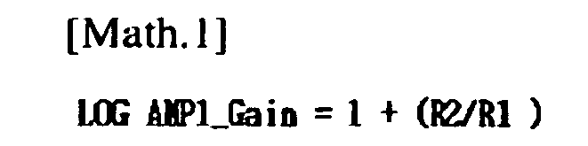
- the amplification gain of the first log amplifier 111B can be controlled by math figure 1 below.
- the amplification gain of the first log amplifier 111B is controlled within the range of about 0 dB-20 dB according to a numerical value of the first resistor R1.
- Fig. 4 is a view illustrating another example of the voltage generator according to the first embodiment.
- the voltage generator 150 can generate a voltage Vo using the electromagnetic energy of a high frequency signal received from the reception antenna 101. That is, the voltage generator 150 is a voltage oscillation circuit or a voltage multiplier circuit; and can be realized using a plurality of detection diodes and capacitors connected in multiple steps. The voltage generator 150 sequentially repeatedly rectifies an RF signal received through the reception antenna 101 into a DC voltage to increase the rectified DC voltage. The voltage generated by the voltage generator 150 is supplied to each part through a logic board.
- Fig. 5 is a construction view of the second to fourth signal processors of Fig. 2 .
- the second signal processor 115 comprises a first operation amplifier 116 and a fourth resistor R4.
- the third signal processor 117 comprises a second operation amplifier 118, a fifth resistor R5, and a third resistor R3.
- the fourth signal processor 119 comprises a first comparator 120, a sixth resistor R6, and a seventh resistor R7.
- the first filter 113 is connected to the positive terminal (+) of the first operation amplifier 116, and the fourth resistor R4 and the third resistor R3 of the negative feedback circuit are connected to the negative terminal (-) of the first operation amplifier 116 in parallel.
- a reference voltage of the first controller 170 is input to the positive terminal (+) of the second operation amplifier 118, and a fifth resistor R5 of the negative feedback circuit is connected to the negative terminal (-) of the second operation amplifier 118.
- the third resistor R3 is connected between the negative terminal (-) of the first operation amplifier 116 and the negative terminal (-) of the second operation amplifier 118.
- the output terminal of the first operation amplifier 116 is connected to the positive terminal (+) of the first comparator 120 through the sixth resistor R6, and connected to the fourth resistor R4 in parallel.
- the output terminal of the second operation amplifier 118 is connected to the negative terminal (-) of the first comparator 120 through the seventh resistor R7.
- the positive terminal (+) and negative terminal (-) of the first comparator 120 can be mutually changed and is not limited thereto.
- the first operation amplifier 116 amplifies the gain of a signal that has passed through the first filter 113 to output the same. At this point, the gain is controlled by the fourth resistor R4 of a first feedback circuit of the first operation amplifier 116.
- the second operation amplifier 118 amplifies the reference voltage of the first controller 170 input to the positive terminal (+) of the second operation amplifier 118 to output the same.
- An output signal of the second operation amplifier 118 controls the level of a signal input to the negative terminal (-) of the first operation amplifier 116 through the fifth resistor R5 of a second feedback circuit, the third resistor R3, which is a feedback circuit, and the fourth resistor R4 of the first feedback circuit.
- the output signal of the second operation amplifier 118 changes according to the reference voltage of the first controller 170.
- the amplification gain of the first operation amplifier 116 is controlled by a change in the output signal of the second operation amplifier 118. That is, the amplification gains of the second operation amplifier 118 and the first operation amplifier 116 are controlled using the reference voltage of the first controller 170, so that the sensitivity of a reception signal output to the first operation amplifier 116 can be controlled.
- the output signals of them can have an inverted phase.
- a signal processed by the first and second operation amplifiers 116 and 118 is a DC level analog signal.
- the output signal of the first operation amplifier 116 is a high level
- the output signal of the second operation amplifier 118 becomes a low level.
- the first comparator 120 of the fourth signal processor 119 compares the output signal of the first operation amplifier 116 with the output signal of the second operation amplifier 118, and outputs a digital signal to the first controller 170 according to the comparison result.
- the first controller 170 can recover a digital signal more completely by delivering synchronization information to the fourth signal processor 119.
- the digital signal of the fourth signal processor 119 is input to the first controller 170 as a tiansistor-transistor logic (TTL)/complementary metal oxide semiconductor (CMOS) signal.
- TTL tiansistor-transistor logic
- CMOS complementary metal oxide semiconductor
- Fig. 6 is a view illustrating a modified example of an antenna of a tag device 100 according to the first embodiment.
- the tag device 100 comprises an IC chip 100B and a single antenna 105.
- the IC chip can comprise the first reception module 110, the first transmission module 130, the first controller 170, and the voltage generator 150 of Fig. 1 .
- the antenna 105 is a transmission/reception antenna, and is formed in a closed loop type, for example, and has a structure in which the IC chip 100B has been mounted between two sides facing each other.
- the IC chip 100B can transmit or receive a signal through the antenna 105, there is no limitation in the structure of the antenna.
- a second embodiment is described with reference to Figs. 7 to 10 .
- Fig. 7 is a construction view of an RFID system according to a second embodiment.
- the RFID system 300A comprises a tag device 100A and a reader device 200A.
- the reader device 200A communicates with the tag device 100A through wireless short distance communication in order to collect information of the tag device 100A.
- the reader device 200A can collect data of the tag device 100A by transmitting an information request signal to the tag device 100A, and receiving object detailed information from the tag device 100A.
- the reader device 200A transmits/ receives the collected information to/from a middle ware or other nodes.
- the RFID system 300A performs communication through at least one RF frequency of an LF of 124-134 kHz, 13.56 MHz, 400-915 MHz, 2.45 GHz, and 5.8 GHz.
- the tag device 100A can operate in at least one of a passive mode, an active mode, and a semi-active mode.
- the tag device 100A can operate in the semi-active mode, that is, in the passive mode and the active mode depending on whether power is supplied as in the tag device of the first embodiment.
- the reader device 200A comprises a second reception module 210, a second transmission module 230, and a second controller 250.
- the second reception module 210 decodes a high frequency signal received through a reception antenna 201 into a digital signal. That is, the reader device 200A decodes a high frequency signal into a digital signal, not using general superheterodyne method, sequential low frequency method, intermediate frequency synthesis method. Accordingly, the circuit of the second reception module 210 can be minimized.
- the second transmission module 230 modulates a digital transmission signal using different modulation methods, separates the modulated signal into an I signal and a Q signal, and transmits the signals through a plurality of transmission antennas 203 and 205. That is, the I signal is transmitted in the form of left hand circular polarization (LHCP) by the first transmission antenna 203, and the Q signal is transmitted in the form of right hand circular polarization (RHCP) by the second transmission antenna 205.
- the transmission antennas 203 and 205 comprise a circularly polarization antenna.
- the second transmission module 230 can use at least two of ASK, FSK, and QPSK.
- the reader device 200A transmits a signal modulated in different modulation methods in the form of the LHCP and the RHCP.
- the modulated signal transmitted from the reader device 200A is received in the tag device 100A.
- the tag device 100A can receive signals having various reception angles, a signal recognition rate can be improved in comparison with the case of receiving one signal.
- the second controller 250 communicates with the tag device 100A through a communication protocol, controls the operations of the second reception module 210 and the second transmission module 230, transmits a periodic information request signal through the second transmission module 230, and stores and analyzes tag information received through the second reception module 210.
- Fig. 8 is a construction view of the reader device of Fig. 7 .
- the reader device 200 comprises the second reception module 210, the second transmission module 230, and the second controller 250.
- the second reception module 210 comprises a fifth signal processor 211, a third filter 213, a sixth signal processor 215, a seventh signal processor 217, and an eighth signal processor 219.
- the fifth to eighth signal processors 211, 215, 217, and 219 decode a received high frequency signal into a digital signal.
- the fifth signal processor 211 filters RF signals in a predetermined frequency band from RF signals received through a reception antenna 201, gain-amplifies the signals, and processes the signals into DC-level analog signals. That is, a received high frequency signal is converted into a log scale by the fifth signal processor 211 and output as a baseband signal.
- the second controller 250 outputs a control signal to the fifth signal processor 211, and the control signal controls the signal gain of the fifth signal processor 211.
- the third filter 213 removes a noise component comprised in the signal processed by the fifth signal processor 211.
- the third filter 213 can be realized using passive devices such as a resistor and a capacitor to remove a ripple of a signal output from the fifth signal processor 211. That is, when a ripple is not sufficiently removed from a reception signal, a difference is generated to the scale of a carrier signal by a direct decoding method. Therefore, the third filter 213 removes the ripple of a reception signal.
- the sixth signal processor 215 controls the gain of the output signal of the third filter 213 to amplify a signal, and the amplified signal is input to the eighth signal processor 219.
- the output of the seventh signal processor 217 changes depending on the reference voltage of the second controller 250, and the changed output is input to the eighth signal processor 219.
- the output signal of the seventh signal processor 217 controls the amplification gain of the sixth signal processor 215, it compensates for the gain of a reception signal according to the various reference voltages of the second controller 250.
- the eighth signal processor 219 compares the amplified signal of the sixth signal processor 215 with the output signal of the seventh signal processor 217 to output a digital signal as a comparison result.
- the digital signal of the eighth signal processor 219 is input to the second controller 250.
- the second controller 250 controls the gain of the fifth signal processor 211 and controls the reference voltage of the seventh signal processor 217 according to the state of a received signal. Accordingly, the second controller 250 can control the sensitivity of a digital signal output to the eighth signal processor 219. Also, the second controller 250 delivers synchronization information to the eighth signal processor 219 to control the comparison operation.
- the second controller 250 collects and stores tag information from the tag device 100A. Also, the second controller 250 can analyze a reception signal decoded by the fifth to eighth signal processors 211, 215, 217, and 219, and communicate with an external interface or other nodes.
- the second transmission module 230 comprises a second phase synchronization circuit 231, a second signal separator 233, a third modulator 235, a third power amplifier 237, a fourth modulator 239, a fourth power amplifier 241, a second coupler 243, and a third signal separator 245.
- the second phase synchronization circuit 231 generates a reference signal to output the same to the second signal separator 233 in response to a control signal of the second controller 250.
- the second signal separator 233 outputs the reference signal to the third modulator 235 and the fourth modulator 239.
- the second signal separator 233 can be realized using a switch device such as a single pole double throw (SPDT) or a coupler, but is not limited thereto.
- the second controller 250 outputs a digital transmission signal, for example, a tag information request signal to the third modulator 235 and/or the fourth modulator 239 of the second transmission module 230. Also, the second controller 250 can send the tag information request signal to the third modulator 235 or the fourth modulator 239, or to the third modulator 235 and the fourth modulator 239 simultaneously, or to the third modulator 235 and the fourth modulator 239 sequentially.
- a digital transmission signal for example, a tag information request signal to the third modulator 235 and/or the fourth modulator 239 of the second transmission module 230.
- the second controller 250 can send the tag information request signal to the third modulator 235 or the fourth modulator 239, or to the third modulator 235 and the fourth modulator 239 simultaneously, or to the third modulator 235 and the fourth modulator 239 sequentially.
- the second controller 250 delivers the tag information request signal to the third modulator 235 and the fourth modulator 239 of the second reception module 230.
- the third modulator 235 modulates a digital transmission signal into a first analog signal using ASK, for example.
- the third modulator 235 can selectively comprise a rectifying filter, a low pass filter, and a level detector, and is not limited to thereto.
- the third power amplifier 237 amplifies the first analog signal modulated by the third modulator 235 to a transmission level, and the amplified signal passes through the second coupler 243 and is delivered to the third signal separator 245.
- the fourth modulator 239 modulates a digital transmission signal into a second analog signal.
- the fourth modulator 239 can modulate a signal using FSK or QPSK for example.
- the fourth modulator 239 can selectively comprise a plurality of mixers, adders, and orthogonal signal conversion circuits.
- the third modulator 235 exemplarily uses ASK modulation
- the fourth modulator 239 exemplarily uses FSK or QPSK modulation
- the third modulator 235 and the fourth modulator 239 can use one of ASK, FSK, and QPSK modulations.
- the third and fourth modulators 235 and 239 use different modulation.
- elements on a transmission path using the third modulator 235 and a transmission path using the fourth modulator 239 can change depending on a transmission frequency. For example, the power amplifier on one of the paths can be removed, and there is no limitation.
- a second analog signal modulated by the fourth modulator 239 is amplified by the fourth power amplifier 241, and the amplified second analog signal is coupled at the second coupler 243, and delivered to the third signal separator 245.
- the second coupler 243 can be connected to one of two input lines, and can couple and output signals input through the two lines.
- the location of the second coupler 243 can change, and can be comprised in the third signal separator 245 and is not limited thereto.
- the second coupler 243 can output a first analog signal or a second analog signal, or couple the first analog signal and the second analog signal to output the same. That is, the form of an analog signal output to the second coupler 243 changes depending on whether the third modulator 235 and the fourth modulator 239 operate.
- the third signal separator 245 can be realized in various circuits such as a circulator, a balloon circuit, a coupler, and polarization diversity, and can be realized using a branch line coupler having an excellent signal separation function or a balloon circuit, for example.
- the third signal separator 245 separates an input first signal into and/or a second analog signal into two signals having a predetermined phase difference (ex: 90°). That is, the first analog signal is separated into a first I signal and a first Q signal. The second analog signal is separated into a second I signal and a second Q signal.
- the I (In-phase) signal and the Q (Quadrature-phase) signal have a phase difference of 90° with respect to each other. For example, when the I signal has a phase of 0°, the Q signal has a phase of 90°.
- a first I signal and/or a second I signal separated by the third signal separator 245 are transmitted through the first transmission antenna 203.
- a first Q signal and/or a second Q signal are transmitted through the second transmission antenna 205.
- the first I signal and the second I signal, the first Q signal and the second Q signal are simultaneously transmitted, or only I/Q signals of one of analog signals can be transmitted, or I/Q signals of the analog signals can be sequentially transmitted.
- the transmission antennas 203 and 205 comprise a plurality of circularly polarized antennas, and transmit different circularly polarized waves.
- the first transmission antenna 203 transmits a first I signal and a second I signal in the form of LHCP
- the second transmission antenna 205 transmits a first Q signal and a second Q signal in the form of RHCP.
- the LHCP and the RHCP do not interfere with each other and form a bean pattern.
- the transmission antennas 203 and 205 can be formed in a dual type patch antenna.
- the reader device 200A can transmit a signal modulated in at least one modulation method in the form of the LHCP and the RHCP, or transmit I and Q signals modulated in different methods in the form of the LHCP and the RHCP.
- a modulation signal transmitted from the reader device 200A is received in the tag device.
- the tag device can receive signals having various reception angles, a signal recognition rate can be improved in comparison with the case of receiving one signal.
- the reader device 200A can remove a phase change by movement of a tag device and remove recognition reduction by an energy delivery position. Also, the second embodiment improves a signal recognition distance, improves an energy supply to the tag device, and improves the reception sensitivity of the tag device by removing a reason why the intensity of a signal reduces as a distance between the reader device 200A and the tag device increases.
- the reader device can stably communicate with the tag device on the whole.
- Fig. 9 is a construction view of the fifth signal processor of Fig. 8 .
- the fifth signal processor 211 comprises a fourth filter 211A, a second log amplifier 211 B, an eleventh resistor R11 and a twelfth resistor R12.
- the fourth filter 211A is connected to the reception antenna 201.
- the positive terminal (+) of the second log amplifier 211B is connected to the fourth filter 211A, and the negative terminal (-) of the log amplifier 211B is connected to the twelfth resistor R 12 of a negative feedback circuit.
- the output terminal of the second log amplifier 211B is connected to the third filter 213 through the eleventh resistor R 11.
- the fourth filter 211A filters signals in a predetermined frequency band from received signals of a mixed noise component.
- the second log amplifier 211B converts a signal output to the fourth filter 211A into a log scale to output the signal into a DC level analog signal, i.e., a baseband signal.
- the second log amplitier 211B can comprise at least one of a gain amplification circuit, a power amplification circuit, and a signal conversion circuit.
- the gain amplification circuit amplifies a signal according to a voltage gain to output an unstable high frequency signal in a state easy to recover.
- a reception signal whose gain has been amplified by the gain amplification circuit has a reduced bit error rate and has a high recognition rate even under a fading environment, so that such a reception signal can be recovered to a stable signal.
- the power amplification circuit secondarily amplifies and outputs the power of a signal whose gain has been amplified by the gain amplification circuit.
- the signal conversion circuit converts an RF signal amplified by the power amplification circuit, for example, a signal in a band of 900 MHz into a DC level analog signal proportional to a decibel value.
- the amplification gain of the second log amplifier 211B can be controlled by the eleventh resistor R11 and the twelfth resistor R12.
- the twelfth resistor R12 has fixed resistance, and the eleventh resistor R11 is a variable resistor whose resistance is varied by the second controller 250.
- the twelfth resistor R12 can be connected between the output terminal of the second log amplifier 211B and a connection point of the negative feedback circuit, or between a connection point of the output terminal of the second log amplifier 211B and the negative feedback circuit, and the third filter 213.
- the eleventh resistor R11 and the twelfth resistor R12 can serve as.a gain control circuit of the second log amplifier 211B.
- the amplification gain of the second log amplifier 211 B can be controlled by math figure 2 below.
- the amplification gain of the second log amplifier 211B is controlled within the range of about 0 dB-20 dB according to a numerical value of the eleventh resistor R11.
- Fig. 10 is a construction view of the sixth to eighth signal processors of Fig. 8 .
- the sixth signal processor 215 comprises a third operation amplifier 216 and a fourteenth resistor R 14.
- the seventh signal processor 217 comprises a fourth operation amplifier 218, a fifteenth resistor R15, and a thirteenth resistor R13.
- the eighth signal processor 219 comprises a second comparator 220, a sixteenth resistor R16, and a seventeenth resistor R17.
- the third filter 213 is connected to the positive terminal (+) of the third operation amplifier 216, and the fourteenth resistor R14 of a third feedback circuit is connected to the negative terminal (-) of the third operation amplifier 216.
- a reference voltage of the second controller 250 is input to the positive terminal (+) of the fourth operation amplifier 218, and the fifteenth resistor R15 of a fourth feedback circuit is connected to the negative terminal (-) of the fourth operation amplifier 218.
- the thirteenth resistor R13 is a feedback circuit, and is connected to the third feedback circuit of the third operation amplifier 216 and to the fourth feedback circuit of the fourth operation amplifier 218.
- the thirteen resistor R13 is disposed in parallel to the fourteenth resistor R14 and the fifteenth resistor R15.
- the output terminal of the third operation amplifier 216 is connected to the positive terminal (+) of the second comparator 220 through the sixteenth resistor R16, and the output terminal of the fourth operation amplifier 218 is connected to the negative terminal (-) of the second comparator 220 through the seventeenth resistor R17.
- the positive terminal (+) and negative terminal (-) of the second comparator 220 can be mutually changed and is not limited thereto.
- the third operation amplifier 216 amplifies the gain of a signal that has passed through the third filter 213 to output the same. At this point, the gain is controlled by the fourteenth resistor R14 of the third feedback circuit of the third operation amplifier 216.
- the output level of the fourth operation amplifier 218 is controlled by the reference voltage of the second controller 250 input to the positive terminal (+) of the fourth operation amplifier 218.
- the output level of the fourth operation amplifier 218 controls the level of the negative terminal (-) of the third operation amplifier 216 through the fifteenth resistor R15, which is the fourth feedback circuit, the thirteenth resistor R13, which is a feedback circuit, and the fourteenth resistor R14, which is the third feedback circuit.
- the amplification gain of the output signal of the third operation amplifier 216 can be controlled according to the reference voltage of the second controller 250 input to the negative terminal (-) of the fourth operation amplifier 218. That is, the amplification gains of the fourth operation amplifier 218 and the third operation amplifier 216 are controlled using the reference voltage of the second controller 250, so that the sensitivity of a reception signal output to the third operation amplifier 216 can be controlled.
- the output signals of them can have an inverted phase.
- a signal processed by the third and fourth operation amplifiers 216 and 218 is a DC level analog signal. Therefore, when the output signal of the third operation amplifier 216 is a high level, the output signal of the fourth operation amplifier 218 becomes a low level.
- the second comparator 220 of the eighth signal processor 219 compares the output signal of the third operation amplifier 216 with the output signal of the fourth operation amplifier 218, and outputs a digital signal to the second controller 250 according to the comparison result.
- the second controller 250 can recover a digital signal more completely by delivering synchronization information to the eighth signal processor 219. That is, the digital signal of the eighth signal processor 219 is input to the second controller 250 as a TTL/CMOS signal.
- the reader device decodes a high frequency signal, and can improve the recognition rate of the tag device by transmitting signals in different modulation methods when modulating a tag request signal.
- the tag device 100 of Fig. 1 described in the first embodiment can be applied as the tag device 100A of Fig. 7 described in the second embodiment
- the reader device 200A of Fig. 7 described in the second embodiment can be applied as the reader device 200 of Fig. 1 described in the first embodiment.
- the elements and the descriptions of the first embodiment, and the elements and the descriptions of the second embodiment are not limited to the relevant embodiment but can be applied to the other embodiment.
- Embodiments decode a received high frequency signal without using an intermediate frequency (IF), low IF, zero IF, so that the number of parts of tag device and the reader device is reduced, and thus the tag device and the reader device can be realized in a simple circuit.
- IF intermediate frequency
- Embodiments can efficiently use the power of the tag device.
- the system can stably maintain communication according to an electromagnetic wave environment.
- Embodiments can improve the signal recognition rates of the tag device and the reader device, and improve reception sensitivity and signal recognition distance.
- Embodiments can modulate transmission signals in various mediation methods, and transmit the signals in a circularly polarized component to provide the reader device that can stably communicate with the tag device.
Landscapes
- Engineering & Computer Science (AREA)
- Physics & Mathematics (AREA)
- General Physics & Mathematics (AREA)
- Theoretical Computer Science (AREA)
- Artificial Intelligence (AREA)
- Computer Vision & Pattern Recognition (AREA)
- Computer Networks & Wireless Communication (AREA)
- Computer Hardware Design (AREA)
- Microelectronics & Electronic Packaging (AREA)
- Near-Field Transmission Systems (AREA)
- Digital Transmission Methods That Use Modulated Carrier Waves (AREA)
Description
- Embodiments relate to a tag device and a reader device.
- Ubiquitous network technology means technology allowing a natural access to various networks without limitation in time and space. Examples of the ubiquitous network technology comprise RFID technology.
- Generally, the RFID technology comprises a tag device and a reader device. The tag device is attached on an object such as goods to record detail information of the object.
- The reader device performs RF communication with the tag device to obtain the information of the object from the tag device. This RFID technology provides an infrastructure on which distribution/circulation management such as distribution, assembly, price change, and selling can be efficiently processed.
- From
WO 2006/059331A2 it is known an autonomous sensing device comprising a receiver with an envelope detector. The envelope detector may include suitable log amplifiers and/or suitable diode and RC circuits. -
US 5 850 416 A discloses a battery-less informative device, wherein RF waves received by an antenna are passed through a bandpass filter in a receiver and then through a logarithmic amplifier. -
US 2006/238308 A1 discloses a transponder apparatus with a receiver, a power source, a processing unit, a buffer device to receive an information signal based on an RF signal from said receiver, to determine whether said information signal includes said identifier and to cause said processing unit to move from said inactive state to said active state. - From "A 0,1 to 2,5 GHZ Lograrythmic Amplifier for RF Detection", Microwave Journal, Horizon House Publications, Norwood, MA, US, vol. 41, no. 7, 1 July 1998, XP000849007, ISSN: 0192-6225 it is known a logarithmic amplifier for radio frequency detection.
- Embodiments provide a tag device and a reader device can decode a received high frequency signal without using an intermediate frequency.
- Embodiments provide a tag device that can efficiently use power by providing various modulation methods and operating in a passive mode modulation method or an active mode modulation method depending on the kind of power.
- Embodiments provide a reader device and an RFID system that can separate transmission signals modulated in various methods into signals of the same phase and orthogonal signals to transmit the signals in the form of circularly polarized waves.
- Embodiments provide a tag device that can stably recover received signals regardless of a phenomenon chat the phase and the energy delivery position of a signal change depending on position movement.
- Embodiments provide a tag device and a reader device that can change a high frequency signal in a direct current (DC) level without using a related an demolulation method that uses a superheterodyne method, a sequential low frequency method, an intermediate frequency synthesis method.
- Embodiments provide a reader device that can stably supply tag energy and improving a signal recognition rate by using various modulation methods and differently processing a signal with consideration of a reception angle.
- The invention provides a tag device comprising the features of clam 1 and a reader device according to claim 8. Further embodiments of the invention are described in the dependent claims.
- The details of one or more embodiments are set forth in the accompanying drawings and the description below. Other features will be apparent from the description and drawings, and from the claims.
- Embodiments can decode a received high frequency signal without using an in termediate frequency (IF), low IF, zero IF to reduce the number of parts of a tag device and a reader device, and realize a simple circuit.
- Embodiments can efficiently use power of a tag device.
- Embodiments can provide various modulation methods to a tag device and/or a reader device to maintain stabile communication according to an electromagnetic wave environment.
- Embodiments can improve the signal recognition rates of a tag device and a reader device, and improve reception sensitivity and a signal recognition distance.
- Embodiments can modulate a transmission signal in various modulation methods, and transmit the transmission signal in a circularly polarized component in a reader device, and provide a reader device that can stably communicate with a tag device.
-
-
Fig. 1 is a construction view of an RFID system according to a first embodiment. -
Fig. 2 is a construction view of the tag device ofFig. 1 . -
Fig. 3 is a construction view of the first signal processor ofFig. 2 . -
Fig. 4 is a construction view illustrating another example of the voltage generator ofFig. 2 . -
Fig. 5 is a construction view of the second to fourth signal processors ofFig. 2 . -
Fig. 6 is a view illustrating an example of an antenna of a tag device according to the first embodiment. -
Fig. 7 is a construction view of an RFID system according to a second embodiment. -
Fig. 8 is a construction view of the reader device ofFig. 7 . -
Fig. 9 is a construction view of the fifth signal processor ofFig. 8 . -
Fig. 10 is a construction view of the sixth to eighth signal processors ofFig. 8 . - Reference will now be made in detail to the embodiments of the present disclosure, examples of which are illustrated in the accompanying drawings.
- The first embodiment is illustrated in
Figs. 1 to 6 .Fig. 1 is a construction view of an RFID system according to the first embodiment, andFig. 2 is a construction view of the tag device ofFig. 1 . - Referring to
Fig. 1 , theRFID system 300 comprises a tag (or transponder)device 100 and a reader (or interrogator)device 200. - The
reader device 200 communicates with thetag device 100 through wireless short distance communication in order to collect information of thetag device 100. For example, thereader device 200 can collect the information of thetag device 100 by transmitting an information request signal to thetag device 100, and receiving object detailed information from thetag device 100. Thereader device 200 transmits/receives the collected information to/from a middle ware or other nodes. - The
tag device 100 has various shapes and sizes, and is classified into an active tag and a passive tag depending on whether power is supplied, classified into a low frequency system and a high frequency system depending on a frequency in use. Thetag device 100 is attached to persons, automobiles, goods, livestock, and buildings, and contains detailed information of a corresponding object. Also, thetag device 100 can be mounted on a smart card to perform user authentication and electronic payment. Thetag device 100 can be attached or function in cooperation with another device to provide various services. - The RF frequency tag of the
RFID system 300 can be classified into a low frequency (LF) tag of 124-134 kHz used for access control and animal management, a high frequency (HF) tag of 13.56 MHz used for an integrated circuit (IC) card and an identification card, an ultra HF (UHF) tag of 400-915 MHz used for identification of containers in distribution and circulation, and a microwave tag of 2.45 GHz. Also, a 5.8 GHz tag can be used for telematics. These communication bands are provided for an exemplary purpose, and can change within the technical scope of the embodiments. - Here, the
tag device 100 can operate in an active mode driven by power supplied from apower unit 155, and a passive mode not requiring power. That is, thetag device 100 can operate in a semi-active mode. Here, when thetag device 100 is mounted on a terminal such as a mobile terminal, thetag device 100 can use the battery power of the mobile terminal as thepower unit 155. - The
tag device 100 comprises afirst reception module 110, afirst transmission module 130, avoltage generator 150, and afirst controller 170. Thefirst reception module 110 can decode high frequency signals received through areception antenna 101, and the decoded signals are delivered to thefirst controller 170. Here, thefirst reception module 110 converts high frequency signals into digital signals using a log amplifier and a comparator. Since thefirst reception module 110 does not use general a superheterodyne method, a sequential low frequency method, an intermediate frequency synthesis method, the number of parts can be reduced and a circuit size can be minimized. - The
controller 170 controls a drive in the active mode or a passive mode depending on whether power is supplied. For example, thetag device 100 is driven by thepower unit 155 during the active mode, and driven by a voltage generated by thevoltage generator 150 during the passive mode. Also, the active mode and the passive mode can be changed depending on whether power is supplied from thepower unit 155, or can be switched from the passive mode to the active mode when power is supplied to thepower unit 155. One of the active mode and the passive mode can be changed to the other according to a manipulation signal of an operator. - The
voltage generator 150 receives a scale signal corresponding to a high frequency signal processed by thefirst reception module 110 to generate a voltage necessary for the tag device. Thevoltage generator 150 supplies a generated voltage to each part through a logic board or thefirst controller 170 of thetag device 100, so that thetag device 100 can operate in the passive mode. - The
voltage generator 150 is a voltage oscillation circuit or a voltage multiplier circuit, and can be realized using a plurality of detection diodes and capacitors connected in multiple steps. - During the passive mode, the
first transmission module 130 transmits a transmission signal through atransmission antenna 103 in a backscatter method. - Here, during the passive mode and the active mode, the
first transmission module 130 uses different modulation methods. For example, thefirst transmission module 130 can use amplitude shift keying (ASK) during the passive mode, and can selectively use frequency shift keying (FSK), quadrature phase shift keying (QPSK), and phase shift keying (PSK) during the active mode. -
Fig. 2 is a construction view of the tag device ofFig. 1 . - Referring to
Fig. 2 , thetag device 100 comprises thefirst reception module 110, thefirst transmission module 130, and thevoltage generator 150. Thefirst reception module 110 comprises afirst signal processor 111, afirst filter 113, asecond signal processor 115, athird signal processor 117, and afourth signal processor 119. - The first to
fourth signal processors - The
first signal processor 111 filters RF signals in a predetermined frequency band from RF signals received through anreception antenna 101, amplifies a gain of the RF signals, and processes the RF signals into DC level analog signals. Thefirst signal processor 111 outputs the high frequency signals into baseband signals using a log amplifier. The log amplifier is applied to a system requiring long distance communication and high sensitivity. An embodiment is described to use the log amplifier. - At this point, the
first controller 170 outputs a control signal to thefirst signal processor 111, and the control signal controls the gain of thefirst signal processor 111. - The
first filter 113 removes a noise component comprised in a signal processed by thefirst signal processor 111. Thefirst filter 113 can be realized using passive elements such as a resistor and a capacitor, and removes a ripple of a signal output from thefirst signal processor 111. That is, when a ripple is not sufficiently removed from a reception signal, a difference is generated to the scale of a carrier signal by a direct decoding method. Therefore, thefilter 113 removes the ripple of a reception signal. Here, thefirst signal processor 111 can rectify an RF signal into a DC to use the DC as a voltage generation source. - The
second signal processor 115 controls the gain of thefirst filter 113 and amplifies a signal, and the amplified signal is input to thefourth signal processor 119. - The output of the
third signal processor 117 changes depending on a reference voltage of thefirst controller 170, and the changed output is output to thefourth signal processor 119. Here, thesecond signal processor 115 controls a signal output from thefirst signal processor 111 using a signal fed back from thethird signal processor 117. At this point, the amplification gain of thesecond signal processor 115 is compensated for according to various reference voltages of thefirst controller 170. - The
fourth signal processor 119 compares an amplified signal of thesecond signal processor 115 with an output signal of thethird signal processor 117 to output a digital signal as a result of the comparison. That is, thefourth signal processor 119 serves as an analog-to-digital converter. A digital signal of thefourth signal processor 119 changes depending on the output level of thethird signal processor 117, and is input to thefirst controller 170. - The
first controller 170 controls the gain of thefirst signal processor 111 depending on a received signal state, and controls the reference voltage of thethird signal processor 117. Accordingly, thefirst controller 170 can control the sensitivity of a digital signal output to thefourth signal processor 119. Also, thefirst controller 170 delivers synchronization information to thefourth signal processor 119 to control a comparison operation. - The
first controller 170 can store tag information. For example, thefirst controller 170 can comprise a memory (not shown), or the tag information can be separately stored. Thefirst controller 170 has a communication protocol to control radio communication with thereader device 200, and provides tag information when an information request signal is received from thereader device 200. Also, thefirst controller 170 analyzes codes of signals decoded by the first tofourth signal processors - The
first transmission module 130 comprises a firstphase synchronization circuit 131, afirst signal separator 133, afirst modulator 135, afirst power amplifier 137, asecond modulator 139, asecond power amplifier 141, and afirst coupler 143. - The first
phase synchronization circuit 131 generates a reference signal under control of thefirst controller 170. Thefirst signal separator 133 outputs the reference signal to thefirst modulator 135 and thesecond modulator 139. Here, thefirst signal separator 133 can be realized using a switch device such as a single pole double throw (SPDT) or a coupler, but is not limited thereto. - Here, the
first controller 170 delivers a digital transmission signal to thefirst modulator 135 and/or thesecond modulator 139 of thefirst transmission module 130. At this point, when the first transmission module is in the passive mode, thefirst modulator 135 operates. When the first transmission module is in the active mode, thesecond modulator 139 operates. - Also, an
interface 160 is connected to a mobile terminal, for example, to receive manipulation signals of the active mode and the passive mode and deliver the signals to thefirst controller 170. Thefirst controller 170 can select the active mode or the passive mode depending on the manipulation signal. That is, during the passive mode, thefirst controller 170 can output a digital transmission signal to thefirst modulator 135, and during the active mode, thefirst controller 170 can output a digital transmission signal to thesecond modulator 139. Embodiments may not use thepower unit 155 and theinterface 160. Since the construction of the tag device may change depending on an installation environment or application service, the embodiments are not limited to using thepower unit 155 and theinterface 160. - Here, the
voltage generator 150 receives an analog signal from thefirst signal processor 111 to multiply the signal in order to generate a voltage. The generated voltage is supplied to each part through thefirst controller 170 of thetag device 100. That is, a voltage for the passive mode is supplied. Thevoltage generator 150 can be realized using a voltage oscillation circuit or a voltage multiplier circuit, for example. Thevoltage generator 150 can comprise a plurality of detection diodes and capacitors connected in a multiple steps. - The
power unit 155 can be realized in a battery and a voltage control circuit and supplies power to each part through thefirst controller 170. Here, through the powers of thevoltage generator 150 and thepower unit 155 have been described to be supplied through thefirst controller 170, this is only one example, the powers can be supplied through a logic board of the device. - The
first modulator 135 modulates a digital transmission signal into a first analog signal using ASK. Thefirst modulator 135 can comprise a rectifying filter, a low pass filter, and a level detector, and is not limited to thereto. - The
first power amplifier 137 amplifies a signal modulated by thefirst modulator 135 to a transmission level, and the amplified signal passes through thefirst coupler 143 and is transmitted through thetransmission antenna 103. - The
second modulator 139 modulates a digital transmission signal into a second analog signal. Thesecond modulator 139 can modulate a signal using FSK or QPSK for example. Thesecond modulator 139 can comprise a plurality of mixers, adders, and orthogonal signal conversion circuits. Thesecond modulator 139 can change the phase of a transmission signal by 90° to convert a signal in the form in which four signals I+, I -, Q+ and Q- are added. - Here, though the
first modulator 135 exemplarily uses ASK modulation, and thesecond modulator 139 exemplarily uses QPSK modulation, thefirst modulator 135 and thesecond modulator 139 can use one of ASK, FSK, and QPSK modulations. The first andsecond modulators - A signal modulated by the
second modulator 139 is amplified by thesecond power amplifier 141, and the amplified signal is coupled to thefirst coupler 143 and transmitted through thetransmission antenna 103. Here, elements on the transmission path using thefirst modulator 135 and the transmission path using thesecond modulator 139 can change depending on a transmission frequency. For example, the power amplifier on one of the paths can be removed. - The above-described
first transmission module 130 can operate in the active mode and the passive mode by the power of thevoltage generator 150 and thepower unit 155. Also, thefirst transmission module 130 can be set to switch to the active mode when power is supplied through thepower unit 155 with the passive mode set as a default. The setting of the passive mode and the active mode can change and is not limited thereto. - The
transmission antenna 103 is connected to thefirst power amplifier 137 or thesecond power amplifier 141 through thefirst coupler 143. - The
tag device 100 can comprise areception antenna 101 and thetransmission antenna 103, or transmit/receive signals using one antenna and a duplexer. There is no limitation in the structure and the number of the antennas. - Since the
tag device 100 according to the first embodiment transmits signals modulated in various modulation methods, it can stably maintain communication according to an electromagnetic wave environment. Also, thetag device 100 can improve the signal recognition rate of the reader device, and improve reception sensitivity and signal recognition distance. -
Fig. 3 is a construction view of the first signal processor ofFig. 2 . - Referring to
Fig. 3 , thefirst signal processor 111 comprises asecond filter 111A, a first log amplifier 111B, resistors R1 and R2. Thesecond filter 111A is connected to thereception antenna 101. The positive terminal (+) of the first log amplifier 111B is connected to thesecond filter 111A, and the negative terminal (-) of the log amplifier 111B is connected to the second resistor R2 of a negative feedback circuit. The output terminal of the first log amplifier 111B is connected to thefirst filter 113 through the first resistor R1. - The
second filter 111A filters signals in a predetermined frequency band from received signals of a mixed noise component. The first log amplifier 111B converts a signal output to thesecond filter 111A into a log scale. That is, the first log amplifier 111B converts a high frequency signal into a scale size to output a DC level analog signal, i.e., a baseband signal. - Also, the first log amplifier 111B can comprise at least one of a gain amplification circuit, a power amplification circuit, and a signal conversion circuit. The gain amplification circuit amplifies a signal according to a voltage gain to output an unstable high frequency signal in a state easy to recover. A reception signal whose gain has been amplified by the gain amplification circuit has a reduced bit error rate and has a high recognition rate even under a fading environment. Such a reception signal can be recovered to a stable signal even in a section where a reception level is about -90 dBm. The power amplification circuit secondarily amplifies and outputs the power of a signal whose gain has been amplified by the gain amplification circuit. The signal conversion circuit converts an RF signal amplified by the power amplification circuit, for example, a signal in a band of 900 MHz into a DC level analog signal proportional to a decibel value.
- The amplification gain of the first log amplifier 111B can be controlled by the first resistor R1 and the second resistor R2. The second resistor R2 has fixed resistance, and the first resistor R1 is a variable resistor whose resistance is varied by the
first controller 170. The second resistor R2 can be connected between the output terminal of the first log amplifier 111B and a connection point of the negative feedback circuit, or between the first resistor R1 and thefirst filter 113. Here, the first resistor R1 and the second resistor R2 connected to the first log amplifier 111B can serve as a gain control circuit of the first log amplifier 111B. - The amplification gain of the first log amplifier 111B can be controlled by math
figure 1 below. For example, the amplification gain of the first log amplifier 111B is controlled within the range of about 0 dB-20 dB according to a numerical value of the first resistor R1. - MathFigure 1
-
Fig. 4 is a view illustrating another example of the voltage generator according to the first embodiment. - Referring to
Fig. 4 , thevoltage generator 150 can generate a voltage Vo using the electromagnetic energy of a high frequency signal received from thereception antenna 101. That is, thevoltage generator 150 is a voltage oscillation circuit or a voltage multiplier circuit; and can be realized using a plurality of detection diodes and capacitors connected in multiple steps. Thevoltage generator 150 sequentially repeatedly rectifies an RF signal received through thereception antenna 101 into a DC voltage to increase the rectified DC voltage. The voltage generated by thevoltage generator 150 is supplied to each part through a logic board. -
Fig. 5 is a construction view of the second to fourth signal processors ofFig. 2 . - Referring to
Fig. 5 , thesecond signal processor 115 comprises afirst operation amplifier 116 and a fourth resistor R4. Thethird signal processor 117 comprises asecond operation amplifier 118, a fifth resistor R5, and a third resistor R3. Thefourth signal processor 119 comprises afirst comparator 120, a sixth resistor R6, and a seventh resistor R7. - The
first filter 113 is connected to the positive terminal (+) of thefirst operation amplifier 116, and the fourth resistor R4 and the third resistor R3 of the negative feedback circuit are connected to the negative terminal (-) of thefirst operation amplifier 116 in parallel. A reference voltage of thefirst controller 170 is input to the positive terminal (+) of thesecond operation amplifier 118, and a fifth resistor R5 of the negative feedback circuit is connected to the negative terminal (-) of thesecond operation amplifier 118. The third resistor R3 is connected between the negative terminal (-) of thefirst operation amplifier 116 and the negative terminal (-) of thesecond operation amplifier 118. The output terminal of thefirst operation amplifier 116 is connected to the positive terminal (+) of thefirst comparator 120 through the sixth resistor R6, and connected to the fourth resistor R4 in parallel. The output terminal of thesecond operation amplifier 118 is connected to the negative terminal (-) of thefirst comparator 120 through the seventh resistor R7. The positive terminal (+) and negative terminal (-) of thefirst comparator 120 can be mutually changed and is not limited thereto. - The
first operation amplifier 116 amplifies the gain of a signal that has passed through thefirst filter 113 to output the same. At this point, the gain is controlled by the fourth resistor R4 of a first feedback circuit of thefirst operation amplifier 116. Thesecond operation amplifier 118 amplifies the reference voltage of thefirst controller 170 input to the positive terminal (+) of thesecond operation amplifier 118 to output the same. An output signal of thesecond operation amplifier 118 controls the level of a signal input to the negative terminal (-) of thefirst operation amplifier 116 through the fifth resistor R5 of a second feedback circuit, the third resistor R3, which is a feedback circuit, and the fourth resistor R4 of the first feedback circuit. Accordingly, the output signal of thesecond operation amplifier 118 changes according to the reference voltage of thefirst controller 170. The amplification gain of thefirst operation amplifier 116 is controlled by a change in the output signal of thesecond operation amplifier 118. That is, the amplification gains of thesecond operation amplifier 118 and thefirst operation amplifier 116 are controlled using the reference voltage of thefirst controller 170, so that the sensitivity of a reception signal output to thefirst operation amplifier 116 can be controlled. - Also, since the negative terminals (-) of the
first operation amplifier 116 and thesecond operation amplifier 118 are connected to each other, the output signals of them can have an inverted phase. For example, a signal processed by the first andsecond operation amplifiers first operation amplifier 116 is a high level, the output signal of thesecond operation amplifier 118 becomes a low level. - The
first comparator 120 of thefourth signal processor 119 compares the output signal of thefirst operation amplifier 116 with the output signal of thesecond operation amplifier 118, and outputs a digital signal to thefirst controller 170 according to the comparison result. Here, thefirst controller 170 can recover a digital signal more completely by delivering synchronization information to thefourth signal processor 119. Here, the digital signal of thefourth signal processor 119 is input to thefirst controller 170 as a tiansistor-transistor logic (TTL)/complementary metal oxide semiconductor (CMOS) signal. -
Fig. 6 is a view illustrating a modified example of an antenna of atag device 100 according to the first embodiment. - Referring to
Fig. 6 , thetag device 100 comprises an IC chip 100B and asingle antenna 105. The IC chip can comprise thefirst reception module 110, thefirst transmission module 130, thefirst controller 170, and thevoltage generator 150 ofFig. 1 . Theantenna 105 is a transmission/reception antenna, and is formed in a closed loop type, for example, and has a structure in which the IC chip 100B has been mounted between two sides facing each other. The IC chip 100B can transmit or receive a signal through theantenna 105, there is no limitation in the structure of the antenna. - A second embodiment is described with reference to
Figs. 7 to 10 . -
Fig. 7 is a construction view of an RFID system according to a second embodiment. - Referring to
Fig. 7 , the RFID system 300A comprises atag device 100A and areader device 200A. Thereader device 200A communicates with thetag device 100A through wireless short distance communication in order to collect information of thetag device 100A. For example, thereader device 200A can collect data of thetag device 100A by transmitting an information request signal to thetag device 100A, and receiving object detailed information from thetag device 100A. Thereader device 200A transmits/ receives the collected information to/from a middle ware or other nodes. - The RFID system 300A performs communication through at least one RF frequency of an LF of 124-134 kHz, 13.56 MHz, 400-915 MHz, 2.45 GHz, and 5.8 GHz.
- The
tag device 100A can operate in at least one of a passive mode, an active mode, and a semi-active mode. Thetag device 100A can operate in the semi-active mode, that is, in the passive mode and the active mode depending on whether power is supplied as in the tag device of the first embodiment. - The
reader device 200A comprises asecond reception module 210, asecond transmission module 230, and asecond controller 250. Thesecond reception module 210 decodes a high frequency signal received through areception antenna 201 into a digital signal. That is, thereader device 200A decodes a high frequency signal into a digital signal, not using general superheterodyne method, sequential low frequency method, intermediate frequency synthesis method. Accordingly, the circuit of thesecond reception module 210 can be minimized. - The
second transmission module 230 modulates a digital transmission signal using different modulation methods, separates the modulated signal into an I signal and a Q signal, and transmits the signals through a plurality oftransmission antennas first transmission antenna 203, and the Q signal is transmitted in the form of right hand circular polarization (RHCP) by thesecond transmission antenna 205. Here, thetransmission antennas - Here, the
second transmission module 230 can use at least two of ASK, FSK, and QPSK. - The
reader device 200A transmits a signal modulated in different modulation methods in the form of the LHCP and the RHCP. The modulated signal transmitted from thereader device 200A is received in thetag device 100A. At this point, since thetag device 100A can receive signals having various reception angles, a signal recognition rate can be improved in comparison with the case of receiving one signal. - The
second controller 250 communicates with thetag device 100A through a communication protocol, controls the operations of thesecond reception module 210 and thesecond transmission module 230, transmits a periodic information request signal through thesecond transmission module 230, and stores and analyzes tag information received through thesecond reception module 210. -
Fig. 8 is a construction view of the reader device ofFig. 7 . - Referring to
Fig. 8 , thereader device 200 comprises thesecond reception module 210, thesecond transmission module 230, and thesecond controller 250. Thesecond reception module 210 comprises afifth signal processor 211, athird filter 213, asixth signal processor 215, aseventh signal processor 217, and aneighth signal processor 219. - The fifth to
eighth signal processors fifth signal processor 211 filters RF signals in a predetermined frequency band from RF signals received through areception antenna 201, gain-amplifies the signals, and processes the signals into DC-level analog signals. That is, a received high frequency signal is converted into a log scale by thefifth signal processor 211 and output as a baseband signal. - At this point, the
second controller 250 outputs a control signal to thefifth signal processor 211, and the control signal controls the signal gain of thefifth signal processor 211. - The
third filter 213 removes a noise component comprised in the signal processed by thefifth signal processor 211. Thethird filter 213 can be realized using passive devices such as a resistor and a capacitor to remove a ripple of a signal output from thefifth signal processor 211. That is, when a ripple is not sufficiently removed from a reception signal, a difference is generated to the scale of a carrier signal by a direct decoding method. Therefore, thethird filter 213 removes the ripple of a reception signal. - The
sixth signal processor 215 controls the gain of the output signal of thethird filter 213 to amplify a signal, and the amplified signal is input to theeighth signal processor 219. - The output of the
seventh signal processor 217 changes depending on the reference voltage of thesecond controller 250, and the changed output is input to theeighth signal processor 219. Here, since the output signal of theseventh signal processor 217 controls the amplification gain of thesixth signal processor 215, it compensates for the gain of a reception signal according to the various reference voltages of thesecond controller 250. - The
eighth signal processor 219 compares the amplified signal of thesixth signal processor 215 with the output signal of theseventh signal processor 217 to output a digital signal as a comparison result. The digital signal of theeighth signal processor 219 is input to thesecond controller 250. At this point, thesecond controller 250 controls the gain of thefifth signal processor 211 and controls the reference voltage of theseventh signal processor 217 according to the state of a received signal. Accordingly, thesecond controller 250 can control the sensitivity of a digital signal output to theeighth signal processor 219. Also, thesecond controller 250 delivers synchronization information to theeighth signal processor 219 to control the comparison operation. - The
second controller 250 collects and stores tag information from thetag device 100A. Also, thesecond controller 250 can analyze a reception signal decoded by the fifth toeighth signal processors - The
second transmission module 230 comprises a secondphase synchronization circuit 231, asecond signal separator 233, athird modulator 235, athird power amplifier 237, afourth modulator 239, afourth power amplifier 241, asecond coupler 243, and athird signal separator 245. - The second
phase synchronization circuit 231 generates a reference signal to output the same to thesecond signal separator 233 in response to a control signal of thesecond controller 250. Thesecond signal separator 233 outputs the reference signal to thethird modulator 235 and thefourth modulator 239. Here, thesecond signal separator 233 can be realized using a switch device such as a single pole double throw (SPDT) or a coupler, but is not limited thereto. - At this point, the
second controller 250 outputs a digital transmission signal, for example, a tag information request signal to thethird modulator 235 and/or thefourth modulator 239 of thesecond transmission module 230. Also, thesecond controller 250 can send the tag information request signal to thethird modulator 235 or thefourth modulator 239, or to thethird modulator 235 and thefourth modulator 239 simultaneously, or to thethird modulator 235 and thefourth modulator 239 sequentially. - The
second controller 250 delivers the tag information request signal to thethird modulator 235 and thefourth modulator 239 of thesecond reception module 230. Thethird modulator 235 modulates a digital transmission signal into a first analog signal using ASK, for example. Thethird modulator 235 can selectively comprise a rectifying filter, a low pass filter, and a level detector, and is not limited to thereto. - The
third power amplifier 237 amplifies the first analog signal modulated by thethird modulator 235 to a transmission level, and the amplified signal passes through thesecond coupler 243 and is delivered to thethird signal separator 245. - The
fourth modulator 239 modulates a digital transmission signal into a second analog signal. Thefourth modulator 239 can modulate a signal using FSK or QPSK for example. Thefourth modulator 239 can selectively comprise a plurality of mixers, adders, and orthogonal signal conversion circuits. - Here, though the
third modulator 235 exemplarily uses ASK modulation, and thefourth modulator 239 exemplarily uses FSK or QPSK modulation, thethird modulator 235 and thefourth modulator 239 can use one of ASK, FSK, and QPSK modulations. The third andfourth modulators third modulator 235 and a transmission path using thefourth modulator 239 can change depending on a transmission frequency. For example, the power amplifier on one of the paths can be removed, and there is no limitation. - A second analog signal modulated by the
fourth modulator 239 is amplified by thefourth power amplifier 241, and the amplified second analog signal is coupled at thesecond coupler 243, and delivered to thethird signal separator 245. Thesecond coupler 243 can be connected to one of two input lines, and can couple and output signals input through the two lines. The location of thesecond coupler 243 can change, and can be comprised in thethird signal separator 245 and is not limited thereto. - The
second coupler 243 can output a first analog signal or a second analog signal, or couple the first analog signal and the second analog signal to output the same. That is, the form of an analog signal output to thesecond coupler 243 changes depending on whether thethird modulator 235 and thefourth modulator 239 operate. - The
third signal separator 245 can be realized in various circuits such as a circulator, a balloon circuit, a coupler, and polarization diversity, and can be realized using a branch line coupler having an excellent signal separation function or a balloon circuit, for example. - The
third signal separator 245 separates an input first signal into and/or a second analog signal into two signals having a predetermined phase difference (ex: 90°). That is, the first analog signal is separated into a first I signal and a first Q signal. The second analog signal is separated into a second I signal and a second Q signal. Here, the I (In-phase) signal and the Q (Quadrature-phase) signal have a phase difference of 90° with respect to each other. For example, when the I signal has a phase of 0°, the Q signal has a phase of 90°. - A first I signal and/or a second I signal separated by the
third signal separator 245 are transmitted through thefirst transmission antenna 203. A first Q signal and/or a second Q signal are transmitted through thesecond transmission antenna 205. Here, the first I signal and the second I signal, the first Q signal and the second Q signal are simultaneously transmitted, or only I/Q signals of one of analog signals can be transmitted, or I/Q signals of the analog signals can be sequentially transmitted. - The
transmission antennas first transmission antenna 203 transmits a first I signal and a second I signal in the form of LHCP, and thesecond transmission antenna 205 transmits a first Q signal and a second Q signal in the form of RHCP. The LHCP and the RHCP do not interfere with each other and form a bean pattern. Thetransmission antennas - The
reader device 200A can transmit a signal modulated in at least one modulation method in the form of the LHCP and the RHCP, or transmit I and Q signals modulated in different methods in the form of the LHCP and the RHCP. A modulation signal transmitted from thereader device 200A is received in the tag device. At this point, since the tag device can receive signals having various reception angles, a signal recognition rate can be improved in comparison with the case of receiving one signal. - The
reader device 200A according to the second embodiment can remove a phase change by movement of a tag device and remove recognition reduction by an energy delivery position. Also, the second embodiment improves a signal recognition distance, improves an energy supply to the tag device, and improves the reception sensitivity of the tag device by removing a reason why the intensity of a signal reduces as a distance between thereader device 200A and the tag device increases. The reader device can stably communicate with the tag device on the whole. -
Fig. 9 is a construction view of the fifth signal processor ofFig. 8 . - Referring to
Fig. 9 , thefifth signal processor 211 comprises afourth filter 211A, a second log amplifier 211 B, an eleventh resistor R11 and a twelfth resistor R12. Thefourth filter 211A is connected to thereception antenna 201. The positive terminal (+) of the second log amplifier 211B is connected to thefourth filter 211A, and the negative terminal (-) of the log amplifier 211B is connected to the twelfth resistor R 12 of a negative feedback circuit. The output terminal of the second log amplifier 211B is connected to thethird filter 213 through the eleventh resistor R 11. - The
fourth filter 211A filters signals in a predetermined frequency band from received signals of a mixed noise component. The second log amplifier 211B converts a signal output to thefourth filter 211A into a log scale to output the signal into a DC level analog signal, i.e., a baseband signal. - The second log amplitier 211B can comprise at least one of a gain amplification circuit, a power amplification circuit, and a signal conversion circuit. The gain amplification circuit amplifies a signal according to a voltage gain to output an unstable high frequency signal in a state easy to recover. A reception signal whose gain has been amplified by the gain amplification circuit has a reduced bit error rate and has a high recognition rate even under a fading environment, so that such a reception signal can be recovered to a stable signal. The power amplification circuit secondarily amplifies and outputs the power of a signal whose gain has been amplified by the gain amplification circuit. The signal conversion circuit converts an RF signal amplified by the power amplification circuit, for example, a signal in a band of 900 MHz into a DC level analog signal proportional to a decibel value.
- The amplification gain of the second log amplifier 211B can be controlled by the eleventh resistor R11 and the twelfth resistor R12. The twelfth resistor R12 has fixed resistance, and the eleventh resistor R11 is a variable resistor whose resistance is varied by the
second controller 250. The twelfth resistor R12 can be connected between the output terminal of the second log amplifier 211B and a connection point of the negative feedback circuit, or between a connection point of the output terminal of the second log amplifier 211B and the negative feedback circuit, and thethird filter 213. Here, the eleventh resistor R11 and the twelfth resistor R12 can serve as.a gain control circuit of the second log amplifier 211B. - The amplification gain of the second log amplifier 211 B can be controlled by math
figure 2 below. For example, the amplification gain of the second log amplifier 211B is controlled within the range of about 0 dB-20 dB according to a numerical value of the eleventh resistor R11. - MathFigure 2

-
Fig. 10 is a construction view of the sixth to eighth signal processors ofFig. 8 . - Referring to
Fig. 10 , thesixth signal processor 215 comprises athird operation amplifier 216 and a fourteenth resistor R 14. Theseventh signal processor 217 comprises afourth operation amplifier 218, a fifteenth resistor R15, and a thirteenth resistor R13. Theeighth signal processor 219 comprises asecond comparator 220, a sixteenth resistor R16, and a seventeenth resistor R17. - The
third filter 213 is connected to the positive terminal (+) of thethird operation amplifier 216, and the fourteenth resistor R14 of a third feedback circuit is connected to the negative terminal (-) of thethird operation amplifier 216. A reference voltage of thesecond controller 250 is input to the positive terminal (+) of thefourth operation amplifier 218, and the fifteenth resistor R15 of a fourth feedback circuit is connected to the negative terminal (-) of thefourth operation amplifier 218. The thirteenth resistor R13 is a feedback circuit, and is connected to the third feedback circuit of thethird operation amplifier 216 and to the fourth feedback circuit of thefourth operation amplifier 218. The thirteen resistor R13 is disposed in parallel to the fourteenth resistor R14 and the fifteenth resistor R15. The output terminal of thethird operation amplifier 216 is connected to the positive terminal (+) of thesecond comparator 220 through the sixteenth resistor R16, and the output terminal of thefourth operation amplifier 218 is connected to the negative terminal (-) of thesecond comparator 220 through the seventeenth resistor R17. The positive terminal (+) and negative terminal (-) of thesecond comparator 220 can be mutually changed and is not limited thereto. - The
third operation amplifier 216 amplifies the gain of a signal that has passed through thethird filter 213 to output the same. At this point, the gain is controlled by the fourteenth resistor R14 of the third feedback circuit of thethird operation amplifier 216. The output level of thefourth operation amplifier 218 is controlled by the reference voltage of thesecond controller 250 input to the positive terminal (+) of thefourth operation amplifier 218. The output level of thefourth operation amplifier 218 controls the level of the negative terminal (-) of thethird operation amplifier 216 through the fifteenth resistor R15, which is the fourth feedback circuit, the thirteenth resistor R13, which is a feedback circuit, and the fourteenth resistor R14, which is the third feedback circuit. Accordingly, the amplification gain of the output signal of thethird operation amplifier 216 can be controlled according to the reference voltage of thesecond controller 250 input to the negative terminal (-) of thefourth operation amplifier 218. That is, the amplification gains of thefourth operation amplifier 218 and thethird operation amplifier 216 are controlled using the reference voltage of thesecond controller 250, so that the sensitivity of a reception signal output to thethird operation amplifier 216 can be controlled. - Also, since the negative terminals (-) of the
third operation amplifier 216 and thefourth operation amplifier 218 are connected to each other through the thirteenth resistor R 13, the output signals of them can have an inverted phase. For example, a signal processed by the third andfourth operation amplifiers third operation amplifier 216 is a high level, the output signal of thefourth operation amplifier 218 becomes a low level. - The
second comparator 220 of theeighth signal processor 219 compares the output signal of thethird operation amplifier 216 with the output signal of thefourth operation amplifier 218, and outputs a digital signal to thesecond controller 250 according to the comparison result. Here, thesecond controller 250 can recover a digital signal more completely by delivering synchronization information to theeighth signal processor 219. That is, the digital signal of theeighth signal processor 219 is input to thesecond controller 250 as a TTL/CMOS signal. - According to the second embodiment, the reader device decodes a high frequency signal, and can improve the recognition rate of the tag device by transmitting signals in different modulation methods when modulating a tag request signal.
- Meanwhile, in the embodiments, the
tag device 100 ofFig. 1 described in the first embodiment can be applied as thetag device 100A ofFig. 7 described in the second embodiment, and thereader device 200A ofFig. 7 described in the second embodiment can be applied as thereader device 200 ofFig. 1 described in the first embodiment. The elements and the descriptions of the first embodiment, and the elements and the descriptions of the second embodiment are not limited to the relevant embodiment but can be applied to the other embodiment. - Although embodiments have been described with reference to a number of illustrative embodiments thereof, it should be understood that numerous other modifications and embodiments can be devised by those skilled in the art that will fall within the scope of the principles of this disclosure. More particularly, various variations and modifications are possible in the component parts and/or arrangements of the subject combination arrangement within the scope of the disclosure, the drawings and the appended claims. In addition to variations and modifications in the component parts and/or arrangements, alternative uses will also be apparent to those skilled in the art.
- Embodiments decode a received high frequency signal without using an intermediate frequency (IF), low IF, zero IF, so that the number of parts of tag device and the reader device is reduced, and thus the tag device and the reader device can be realized in a simple circuit.
- Embodiments can efficiently use the power of the tag device.
- Since embodiments provide various modulation methods to the tag device and/or the reader device, the system can stably maintain communication according to an electromagnetic wave environment.
- Embodiments can improve the signal recognition rates of the tag device and the reader device, and improve reception sensitivity and signal recognition distance.
- Embodiments can modulate transmission signals in various mediation methods, and transmit the signals in a circularly polarized component to provide the reader device that can stably communicate with the tag device.
Claims (11)
- A tag device (100) comprising:a reception module (110) comprising a first signal processing means (111) for converting a received high frequency signal into a DC level analog signal according to a log scale by using a log amplifier (111B) that receives the received high frequency signal through its positive terminal;a transmission module (130) for modulating a transmission signal to output the same; anda controller (170) for controlling the reception module (110) and the transmission module (130),characterized in thatthe first signal processing means (111) comprises:a gain control circuit (R1,R2) connected between an output terminal and a negative terminal of the log amplifier (111B) and controlling an amplification gain of the log amplifier (111B) using a resistance (R1) varied by the controller (170);the reception module (110) further comprises:a second signal processing means (115) for amplifying the DC level analog signal converted by the first signal processing means (111),a third signal processing means (117) for controlling a signal level and a gain of the second signal processing means (115) under control of the controller (170), anda fourth signal processing means (119) for converting the amplified DC level analog signal output by the second signal processing means (115) according to an output signal of the third signal processing means (117) so as to output a digital signal; andwherein the controller (170) controls an operation in one of a passive mode and an active mode depending on whether battery power is supplied, and selects a different modulation method for a transmission of a transmission signal depending on each mode.
- The tag device (100) according to claim 1, wherein the transmission module (130) uses amplitude shift keying (ASK) when the transmission module (130) is not driven by power supplied from the battery and selectively uses frequency shift keying (FSK), quadrature phase shift keying (QPSK), and phase shift keying (PSK) when the transmission module (130) is driven by power supplied from the battery.
- The tag device (100) according to claim 1, wherein the second signal processing means (115) comprises:a first operation amplifier (116) for amplifying an output signal of the first signal processing means (111) and outputting the same; anda first feedback circuit (R4) connected between an output terminal and a negative terminal of the first operation amplifier (116), and whereinthe third signal processing means (117) comprises:a second operation amplifier (118) for amplifying a reference voltage of the controller (170) and outputting the same;a second feedback circuit (R5) connected between an output terminal and a negative terminal of the second operation amplifier (118); anda feedback circuit (R3) feeding back a signal of the second feedback circuit to the first feedback circuit.
- The tag device (100) according to claim 1, wherein the fourth signal processing means (119) comprises a comparator (120) comparing an output signal of the second signal processing means (115) with an output signal of the third signal processing means (117) to output said digital signal to the controller (170).
- The tag device (100) according to claim 1, comprising a voltage generator 150) for receiving an output of the log amplifier (111B) to generate a voltage, and for supplying the voltage to each element through the controller (170).
- The tag device (100) according to claim 1, comprising a first filter (113) for removing a noise from the DC level analog signal, the first signal processing means (111) further comprising a second filter (111A) passing signals in a predetermined band from received signals.
- The tag (100) device according to claim 1, wherein the transmission module (130) comprises:a first modulator (135) for modulating the transmission signal;a first amplifier (137) for amplifying the signal modulated by the first modulator (135);a second modulator (139) for modulating the transmission signal;a second amplifier (141) for amplifying the signal modulated by the second modulator (139); anda coupler (143) for outputting at least one of signals amplified by the first amplifier (137) and the second amplifier (141) to an antenna (103).
- A reader device (200A) comprising:a reception module (210) comprising a first signal processing means (211) for converting a received high frequency signal into a DC level analog signal according to a log scale by using a log amplifiers (211B) that receives the received high frequency signal through its positive terminal;a transmission module (230) for modulating an information request signal to output the same; anda controller (250) for controlling the reception module (210) and the transmission module (230),characterized in thatthe first signal processing means (211) comprising:a gain control circuit (R11, R12) connected between an output terminal and a negative 2 terminal of the log amplifier (211B), and controlling an amplification gain of the log amplifier (211B) using a resistance (R11) varied by the controller (250);the reception module (210) further comprises: a second signal processing means (215) for amplifying the DC level analog signal converted by the first signal processing means (211);a third signal processing means (217) for controlling a signal level and a gain of the second signal processing means (215) under control of the controller (250); anda fourth signal processing means (219) for converting the amplified DC level analog signal output by the second signal processing means (215) according to an output signal of the third signal processing means (217) so as to output a digital signal; andwherein the second transmission module (230) modulates a digital transmission signal using different modulation methods, separates the modulated signal into a first signal (I) and a second signal (Q), and transmits the signals (I, Q) through a plurality of transmission antennas (203, 205).
- The reader device (200A) according to claim 10, wherein the reader device (200A) transmits a signal modulated in different modulation methods in the form of the left hand circular polarization (LHCP) and the right hand circular polarization (RHCP).
- The reader device (200A) according to claim 8, wherein the transmission module (230) comprises:a first modulator (235) for modulating the information request signal;a second modulator (239) for modulating the information request signal;a coupler (243) for outputting at least one of signals output by the first modulator (235) and the second modulator (239); anda signal separator (245) for separating output signals of the coupler (243) into a signal of the same phase and an orthogonal signal, and transmitting the signal through an antenna (203, 205).
- The reader device (200A) according to claim 10, wherein the signal of the same phase separated by the signal separator (245) of the transmission module (230) is transmitted through a first transmission antenna (203), and the orthogonal signal is transmitted through a second transmission antenna (205), and the first and second transmission antennas (203, 205) comprise a circular polarized antenna,
wherein the first modulator (235) comprises an amplitude shift keying modulation method, and the second modulator (239) comprises one of a frequency shift keying modulation method and a quadrature phase shift keying modulation method.
Applications Claiming Priority (3)
| Application Number | Priority Date | Filing Date | Title |
|---|---|---|---|
| KR1020070056255A KR101294492B1 (en) | 2007-06-08 | 2007-06-08 | Radio Frequency IDentification transmitter/receiver device |
| KR1020070071013A KR100911821B1 (en) | 2007-07-16 | 2007-07-16 | RFID tag |
| PCT/KR2008/003209 WO2008150147A1 (en) | 2007-06-08 | 2008-06-09 | Tag device, reader device, and rfid system |
Publications (3)
| Publication Number | Publication Date |
|---|---|
| EP2057589A1 EP2057589A1 (en) | 2009-05-13 |
| EP2057589A4 EP2057589A4 (en) | 2011-10-19 |
| EP2057589B1 true EP2057589B1 (en) | 2014-05-07 |
Family
ID=40093882
Family Applications (1)
| Application Number | Title | Priority Date | Filing Date |
|---|---|---|---|
| EP08766171.6A Ceased EP2057589B1 (en) | 2007-06-08 | 2008-06-09 | Tag device, reader device, and rfid system |
Country Status (4)
| Country | Link |
|---|---|
| US (1) | US8292175B2 (en) |
| EP (1) | EP2057589B1 (en) |
| JP (1) | JP2010530098A (en) |
| WO (1) | WO2008150147A1 (en) |
Cited By (1)
| Publication number | Priority date | Publication date | Assignee | Title |
|---|---|---|---|---|
| CN104506536A (en) * | 2014-12-26 | 2015-04-08 | 活点信息技术有限公司 | Internet-of-Things safety analyzer |
Families Citing this family (14)
| Publication number | Priority date | Publication date | Assignee | Title |
|---|---|---|---|---|
| EP2501093B1 (en) * | 2011-03-16 | 2019-06-05 | BlackBerry Limited | Quadrature communications device with I antennas and Q antennas and modulated power supply and related methods |
| US8588330B2 (en) | 2011-03-16 | 2013-11-19 | Blackberry Limited | Quadrature communications device with I antennas and Q antennas and related methods |
| US8553802B2 (en) | 2011-03-16 | 2013-10-08 | Blackberry Limited | Quadrature communications device with I antennas and Q antennas and modulated power supply and related methods |
| EP2501094B1 (en) * | 2011-03-16 | 2016-12-07 | BlackBerry Limited | Quadrature communications device with i antennas and q antennas and related methods |
| US8844830B2 (en) * | 2012-01-20 | 2014-09-30 | Alien Technology Corporation | Persistent nodes for RFID |
| US8833666B2 (en) * | 2012-03-09 | 2014-09-16 | Infineon Technologies Ag | Smart card device |
| CN103870864B (en) * | 2012-12-10 | 2016-09-28 | 首崴电子股份有限公司 | Active electronic labeling device for memory card |
| SI24283A (en) * | 2013-01-15 | 2014-07-31 | Ams R&D Analogni Polprevodniki, D.O.O. | Procedure and circuit of the active smart tag for communication with the interrogator |
| CN103106382A (en) * | 2013-01-31 | 2013-05-15 | 广州梦龙科技有限公司 | Peripheral intelligent reader with radio frequency identification (RFID) recognition function |
| DE102013105291B4 (en) * | 2013-05-23 | 2017-12-07 | Infineon Technologies Ag | smart card |
| KR102139552B1 (en) | 2014-04-11 | 2020-07-31 | 삼성전자주식회사 | Wireless communication device and operating method thereof |
| KR101983827B1 (en) * | 2017-08-30 | 2019-09-03 | 조경환 | Car parking management system |
| CN107977690B (en) * | 2017-12-28 | 2024-05-10 | 深圳市航天华拓科技有限公司 | RFID card sender |
| CN111596588B (en) * | 2020-05-27 | 2025-03-11 | 达仁智能科技(佛山)有限公司 | A microwave sensor and its control circuit |
Family Cites Families (18)
| Publication number | Priority date | Publication date | Assignee | Title |
|---|---|---|---|---|
| EP0011418A1 (en) | 1978-11-20 | 1980-05-28 | THE GENERAL ELECTRIC COMPANY, p.l.c. | Manufacture of electroluminescent display devices |
| DE69015535T2 (en) * | 1989-03-28 | 1995-08-10 | Nippon Telegraph And Telephone Corp., Tokio/Tokyo | DIVERSITY RECEIVER. |
| US5499124A (en) | 1990-12-31 | 1996-03-12 | Vu; Duy-Phach | Polysilicon transistors formed on an insulation layer which is adjacent to a liquid crystal material |
| BR9204795A (en) * | 1991-04-29 | 1993-07-13 | Motorola Inc | CIRCUIT AND PROCESS TO INDICATE INTERFERENCE LEVEL, AND COMMUNICATION DEVICE |
| US5850416A (en) | 1993-06-30 | 1998-12-15 | Lucent Technologies, Inc. | Wireless transmitter-receiver information device |
| JPH0730338A (en) * | 1993-07-07 | 1995-01-31 | Mitsubishi Electric Corp | Input signal switching circuit |
| KR20000074437A (en) * | 1999-05-20 | 2000-12-15 | 구관영 | Interference cancellation system with phase compensation circuitry |
| EP2287777A1 (en) * | 2001-02-12 | 2011-02-23 | Symbol Technologies, Inc. | Radio frequency identification architecture |
| WO2003017320A1 (en) | 2001-08-21 | 2003-02-27 | Nam-Young Kim | Lamp utilizing a light emitted diode |
| US7036679B2 (en) * | 2002-06-24 | 2006-05-02 | John Baranowski | Dispensing and diversion systems and methods |
| DE112005003031T5 (en) | 2004-12-01 | 2007-11-08 | Given Imaging Ltd. | Two-way communication in an autonomous device in the living organism |
| US7375637B2 (en) | 2005-04-21 | 2008-05-20 | University Of Pittsburgh Of The Commonwealth Of Pennsylvania | Methods and apparatus for reducing power consumption of an active transponder |
| KR101114179B1 (en) * | 2005-06-17 | 2012-02-22 | 엘지이노텍 주식회사 | Amplitude shift keying demodulater using sensitivity elevation technology of Radio Fruquency IDentification reader |
| KR100748247B1 (en) | 2005-07-06 | 2007-08-09 | 삼성전기주식회사 | Nitride-based semiconductor light emitting diodes and manufacturing method thereof |
| JP2007064765A (en) | 2005-08-30 | 2007-03-15 | Fujitsu Ltd | RFID tag device, RFID reader / writer device, and distance measurement system |
| US20070215881A1 (en) | 2006-03-03 | 2007-09-20 | Semiconductor Energy Laboratory Co., Ltd. | Light-emitting element and manufacturing method thereof |
| KR100680501B1 (en) | 2006-03-08 | 2007-02-08 | 엘지이노텍 주식회사 | Dual Phase Synchronous Circuit RDF System |
| JP2010517273A (en) | 2007-01-22 | 2010-05-20 | クリー レッド ライティング ソリューションズ、インコーポレイテッド | Fault tolerant illuminant, system including fault tolerant illuminant and method for making fault tolerant illuminant |
-
2008
- 2008-06-09 EP EP08766171.6A patent/EP2057589B1/en not_active Ceased
- 2008-06-09 US US12/442,856 patent/US8292175B2/en not_active Expired - Fee Related
- 2008-06-09 JP JP2010511128A patent/JP2010530098A/en active Pending
- 2008-06-09 WO PCT/KR2008/003209 patent/WO2008150147A1/en not_active Ceased
Cited By (1)
| Publication number | Priority date | Publication date | Assignee | Title |
|---|---|---|---|---|
| CN104506536A (en) * | 2014-12-26 | 2015-04-08 | 活点信息技术有限公司 | Internet-of-Things safety analyzer |
Also Published As
| Publication number | Publication date |
|---|---|
| US20100072277A1 (en) | 2010-03-25 |
| WO2008150147A1 (en) | 2008-12-11 |
| US8292175B2 (en) | 2012-10-23 |
| EP2057589A1 (en) | 2009-05-13 |
| EP2057589A4 (en) | 2011-10-19 |
| JP2010530098A (en) | 2010-09-02 |
Similar Documents
| Publication | Publication Date | Title |
|---|---|---|
| EP2057589B1 (en) | Tag device, reader device, and rfid system | |
| CN102999776B (en) | There are the contact-free integrated circuits of NFC and UHF operator scheme | |
| US10721606B2 (en) | Mobile terminal and method involving near field communication | |
| EP1830301B1 (en) | RFID reader architecture | |
| EP2220792B1 (en) | Near field radio frequency communication system | |
| US8838047B2 (en) | Dynamic RF front end | |
| US20130316648A1 (en) | Wireless communication device with rfid reader | |
| KR20080097115A (en) | Radio frequency identification device | |
| US20140227973A1 (en) | Configuration of nfc routers for p2p communication | |
| KR100911821B1 (en) | RFID tag | |
| KR101294492B1 (en) | Radio Frequency IDentification transmitter/receiver device | |
| KR101114158B1 (en) | RFID transceiver of TDR structure | |
| KR101189400B1 (en) | RFID Reader | |
| EP4625830A1 (en) | Radiofrequency device with three operating modes | |
| CN100542061C (en) | wireless communication equipment | |
| HK1180089A (en) | Contactless integrated circuit having nfc and uhf operating modes | |
| JP2009130604A (en) | Wireless receiving device and wireless tag communication device | |
| WO2012074484A1 (en) | A multiple antenna interface adaptor |
Legal Events
| Date | Code | Title | Description |
|---|---|---|---|
| PUAI | Public reference made under article 153(3) epc to a published international application that has entered the european phase |
Free format text: ORIGINAL CODE: 0009012 |
|
| 17P | Request for examination filed |
Effective date: 20090320 |
|
| AK | Designated contracting states |
Kind code of ref document: A1 Designated state(s): DE GB |
|
| AX | Request for extension of the european patent |
Extension state: AL BA MK RS |
|
| RAP1 | Party data changed (applicant data changed or rights of an application transferred) |
Owner name: LG INNOTEK CO., LTD. |
|
| REG | Reference to a national code |
Ref country code: DE Ref legal event code: R079 Ref document number: 602008032096 Country of ref document: DE Free format text: PREVIOUS MAIN CLASS: G06K0019077000 Ipc: G06K0019070000 |
|
| A4 | Supplementary search report drawn up and despatched |
Effective date: 20110920 |
|
| RIC1 | Information provided on ipc code assigned before grant |
Ipc: G06K 7/00 20060101ALI20110914BHEP Ipc: G06K 19/07 20060101AFI20110914BHEP |
|
| DAX | Request for extension of the european patent (deleted) | ||
| 17Q | First examination report despatched |
Effective date: 20120802 |
|
| GRAP | Despatch of communication of intention to grant a patent |
Free format text: ORIGINAL CODE: EPIDOSNIGR1 |
|
| INTG | Intention to grant announced |
Effective date: 20130531 |
|
| GRAP | Despatch of communication of intention to grant a patent |
Free format text: ORIGINAL CODE: EPIDOSNIGR1 |
|
| INTG | Intention to grant announced |
Effective date: 20131209 |
|
| GRAS | Grant fee paid |
Free format text: ORIGINAL CODE: EPIDOSNIGR3 |
|
| GRAA | (expected) grant |
Free format text: ORIGINAL CODE: 0009210 |
|
| AK | Designated contracting states |
Kind code of ref document: B1 Designated state(s): DE GB |
|
| REG | Reference to a national code |
Ref country code: GB Ref legal event code: FG4D |
|
| REG | Reference to a national code |
Ref country code: DE Ref legal event code: R096 Ref document number: 602008032096 Country of ref document: DE Effective date: 20140612 |
|
| REG | Reference to a national code |
Ref country code: DE Ref legal event code: R097 Ref document number: 602008032096 Country of ref document: DE |
|
| PLBE | No opposition filed within time limit |
Free format text: ORIGINAL CODE: 0009261 |
|
| STAA | Information on the status of an ep patent application or granted ep patent |
Free format text: STATUS: NO OPPOSITION FILED WITHIN TIME LIMIT |
|
| 26N | No opposition filed |
Effective date: 20150210 |
|
| REG | Reference to a national code |
Ref country code: DE Ref legal event code: R097 Ref document number: 602008032096 Country of ref document: DE Effective date: 20150210 |
|
| REG | Reference to a national code |
Ref country code: GB Ref legal event code: 732E Free format text: REGISTERED BETWEEN 20200305 AND 20200311 |
|
| PGFP | Annual fee paid to national office [announced via postgrant information from national office to epo] |
Ref country code: DE Payment date: 20200605 Year of fee payment: 13 |
|
| PGFP | Annual fee paid to national office [announced via postgrant information from national office to epo] |
Ref country code: GB Payment date: 20200608 Year of fee payment: 13 |
|
| REG | Reference to a national code |
Ref country code: DE Ref legal event code: R082 Ref document number: 602008032096 Country of ref document: DE Representative=s name: VIERING, JENTSCHURA & PARTNER MBB PATENT- UND , DE Ref country code: DE Ref legal event code: R081 Ref document number: 602008032096 Country of ref document: DE Owner name: ATEC AP CO., LTD., SEONGNAM-SI, KR Free format text: FORMER OWNER: LG INNOTEK CO., LTD., SEOUL, KR |
|
| REG | Reference to a national code |
Ref country code: DE Ref legal event code: R119 Ref document number: 602008032096 Country of ref document: DE |
|
| GBPC | Gb: european patent ceased through non-payment of renewal fee |
Effective date: 20210609 |
|
| PG25 | Lapsed in a contracting state [announced via postgrant information from national office to epo] |
Ref country code: GB Free format text: LAPSE BECAUSE OF NON-PAYMENT OF DUE FEES Effective date: 20210609 Ref country code: DE Free format text: LAPSE BECAUSE OF NON-PAYMENT OF DUE FEES Effective date: 20220101 |