EP1798599B1 - Antireflection film composition, patterning process and substrate using the same - Google Patents
Antireflection film composition, patterning process and substrate using the same Download PDFInfo
- Publication number
- EP1798599B1 EP1798599B1 EP06025581A EP06025581A EP1798599B1 EP 1798599 B1 EP1798599 B1 EP 1798599B1 EP 06025581 A EP06025581 A EP 06025581A EP 06025581 A EP06025581 A EP 06025581A EP 1798599 B1 EP1798599 B1 EP 1798599B1
- Authority
- EP
- European Patent Office
- Prior art keywords
- group
- film
- organic
- antireflection film
- resist
- Prior art date
- Legal status (The legal status is an assumption and is not a legal conclusion. Google has not performed a legal analysis and makes no representation as to the accuracy of the status listed.)
- Not-in-force
Links
- 239000000203 mixture Substances 0.000 title claims description 219
- 238000000034 method Methods 0.000 title claims description 60
- 239000000758 substrate Substances 0.000 title claims description 52
- 230000008569 process Effects 0.000 title claims description 42
- 238000000059 patterning Methods 0.000 title claims description 20
- 229920000642 polymer Polymers 0.000 claims description 122
- 125000000962 organic group Chemical group 0.000 claims description 58
- 125000004432 carbon atom Chemical group C* 0.000 claims description 57
- 238000005530 etching Methods 0.000 claims description 56
- 229920002120 photoresistant polymer Polymers 0.000 claims description 54
- 239000002253 acid Substances 0.000 claims description 49
- 239000004971 Cross linker Substances 0.000 claims description 43
- 239000003960 organic solvent Substances 0.000 claims description 30
- 125000003545 alkoxy group Chemical group 0.000 claims description 28
- 125000002887 hydroxy group Chemical group [H]O* 0.000 claims description 28
- 238000004132 cross linking Methods 0.000 claims description 27
- GWEVSGVZZGPLCZ-UHFFFAOYSA-N Titan oxide Chemical compound O=[Ti]=O GWEVSGVZZGPLCZ-UHFFFAOYSA-N 0.000 claims description 25
- 125000000217 alkyl group Chemical group 0.000 claims description 25
- 238000001459 lithography Methods 0.000 claims description 25
- OGIDPMRJRNCKJF-UHFFFAOYSA-N titanium oxide Inorganic materials [Ti]=O OGIDPMRJRNCKJF-UHFFFAOYSA-N 0.000 claims description 25
- 239000002738 chelating agent Substances 0.000 claims description 21
- 125000001997 phenyl group Chemical group [H]C1=C([H])C([H])=C(*)C([H])=C1[H] 0.000 claims description 21
- -1 perfluoro compounds Chemical class 0.000 description 130
- 239000000243 solution Substances 0.000 description 88
- 239000010410 layer Substances 0.000 description 70
- LFQSCWFLJHTTHZ-UHFFFAOYSA-N Ethanol Chemical compound CCO LFQSCWFLJHTTHZ-UHFFFAOYSA-N 0.000 description 48
- 230000000052 comparative effect Effects 0.000 description 43
- 229920005989 resin Polymers 0.000 description 38
- 239000011347 resin Substances 0.000 description 38
- OKKJLVBELUTLKV-UHFFFAOYSA-N Methanol Chemical compound OC OKKJLVBELUTLKV-UHFFFAOYSA-N 0.000 description 33
- 238000004519 manufacturing process Methods 0.000 description 32
- XUIMIQQOPSSXEZ-UHFFFAOYSA-N Silicon Chemical compound [Si] XUIMIQQOPSSXEZ-UHFFFAOYSA-N 0.000 description 29
- LLHKCFNBLRBOGN-UHFFFAOYSA-N propylene glycol methyl ether acetate Chemical compound COCC(C)OC(C)=O LLHKCFNBLRBOGN-UHFFFAOYSA-N 0.000 description 29
- RTAQQCXQSZGOHL-UHFFFAOYSA-N Titanium Chemical compound [Ti] RTAQQCXQSZGOHL-UHFFFAOYSA-N 0.000 description 28
- 150000004756 silanes Chemical class 0.000 description 27
- YRKCREAYFQTBPV-UHFFFAOYSA-N acetylacetone Chemical compound CC(=O)CC(C)=O YRKCREAYFQTBPV-UHFFFAOYSA-N 0.000 description 26
- 150000001875 compounds Chemical class 0.000 description 26
- 229910052710 silicon Inorganic materials 0.000 description 26
- 239000000178 monomer Substances 0.000 description 24
- 239000010703 silicon Substances 0.000 description 24
- 239000010936 titanium Substances 0.000 description 23
- KPUWHANPEXNPJT-UHFFFAOYSA-N disiloxane Chemical class [SiH3]O[SiH3] KPUWHANPEXNPJT-UHFFFAOYSA-N 0.000 description 22
- VYPSYNLAJGMNEJ-UHFFFAOYSA-N Silicium dioxide Chemical compound O=[Si]=O VYPSYNLAJGMNEJ-UHFFFAOYSA-N 0.000 description 20
- 239000007789 gas Substances 0.000 description 20
- 239000007787 solid Substances 0.000 description 20
- 239000012212 insulator Substances 0.000 description 19
- 229910052719 titanium Inorganic materials 0.000 description 19
- XEKOWRVHYACXOJ-UHFFFAOYSA-N Ethyl acetate Chemical compound CCOC(C)=O XEKOWRVHYACXOJ-UHFFFAOYSA-N 0.000 description 18
- 238000004321 preservation Methods 0.000 description 18
- 238000001312 dry etching Methods 0.000 description 16
- 229910001868 water Inorganic materials 0.000 description 16
- CSCPPACGZOOCGX-UHFFFAOYSA-N Acetone Chemical compound CC(C)=O CSCPPACGZOOCGX-UHFFFAOYSA-N 0.000 description 15
- 238000006243 chemical reaction Methods 0.000 description 15
- 125000002496 methyl group Chemical group [H]C([H])([H])* 0.000 description 15
- XLYOFNOQVPJJNP-UHFFFAOYSA-N water Substances O XLYOFNOQVPJJNP-UHFFFAOYSA-N 0.000 description 15
- 239000002585 base Substances 0.000 description 14
- 239000002356 single layer Substances 0.000 description 14
- RTZKZFJDLAIYFH-UHFFFAOYSA-N Diethyl ether Chemical compound CCOCC RTZKZFJDLAIYFH-UHFFFAOYSA-N 0.000 description 13
- 239000003054 catalyst Substances 0.000 description 13
- UHOVQNZJYSORNB-UHFFFAOYSA-N Benzene Chemical compound C1=CC=CC=C1 UHOVQNZJYSORNB-UHFFFAOYSA-N 0.000 description 12
- LYCAIKOWRPUZTN-UHFFFAOYSA-N Ethylene glycol Chemical compound OCCO LYCAIKOWRPUZTN-UHFFFAOYSA-N 0.000 description 12
- 239000006096 absorbing agent Substances 0.000 description 12
- 229910021642 ultra pure water Inorganic materials 0.000 description 12
- 239000012498 ultrapure water Substances 0.000 description 12
- BLRPTPMANUNPDV-UHFFFAOYSA-N Silane Chemical compound [SiH4] BLRPTPMANUNPDV-UHFFFAOYSA-N 0.000 description 11
- 229910000077 silane Inorganic materials 0.000 description 11
- 239000000126 substance Substances 0.000 description 11
- ZNOCGWVLWPVKAO-UHFFFAOYSA-N trimethoxy(phenyl)silane Chemical compound CO[Si](OC)(OC)C1=CC=CC=C1 ZNOCGWVLWPVKAO-UHFFFAOYSA-N 0.000 description 11
- 230000000903 blocking effect Effects 0.000 description 10
- 238000009833 condensation Methods 0.000 description 10
- 230000005494 condensation Effects 0.000 description 10
- LZCLXQDLBQLTDK-UHFFFAOYSA-N ethyl 2-hydroxypropanoate Chemical compound CCOC(=O)C(C)O LZCLXQDLBQLTDK-UHFFFAOYSA-N 0.000 description 10
- 230000003301 hydrolyzing effect Effects 0.000 description 10
- 239000012044 organic layer Substances 0.000 description 10
- 229910052814 silicon oxide Inorganic materials 0.000 description 10
- WGTYBPLFGIVFAS-UHFFFAOYSA-M tetramethylammonium hydroxide Chemical compound [OH-].C[N+](C)(C)C WGTYBPLFGIVFAS-UHFFFAOYSA-M 0.000 description 10
- DQZNLOXENNXVAD-UHFFFAOYSA-N trimethoxy-[2-(7-oxabicyclo[4.1.0]heptan-4-yl)ethyl]silane Chemical compound C1C(CC[Si](OC)(OC)OC)CCC2OC21 DQZNLOXENNXVAD-UHFFFAOYSA-N 0.000 description 10
- LJHFIVQEAFAURQ-ZPUQHVIOSA-N (NE)-N-[(2E)-2-hydroxyiminoethylidene]hydroxylamine Chemical class O\N=C\C=N\O LJHFIVQEAFAURQ-ZPUQHVIOSA-N 0.000 description 9
- QTBSBXVTEAMEQO-UHFFFAOYSA-N Acetic acid Chemical compound CC(O)=O QTBSBXVTEAMEQO-UHFFFAOYSA-N 0.000 description 9
- YXFVVABEGXRONW-UHFFFAOYSA-N Toluene Chemical compound CC1=CC=CC=C1 YXFVVABEGXRONW-UHFFFAOYSA-N 0.000 description 9
- VLKZOEOYAKHREP-UHFFFAOYSA-N n-Hexane Chemical compound CCCCCC VLKZOEOYAKHREP-UHFFFAOYSA-N 0.000 description 9
- 239000002904 solvent Substances 0.000 description 9
- 125000000999 tert-butyl group Chemical group [H]C([H])([H])C(*)(C([H])([H])[H])C([H])([H])[H] 0.000 description 9
- MWPLVEDNUUSJAV-UHFFFAOYSA-N anthracene Chemical compound C1=CC=CC2=CC3=CC=CC=C3C=C21 MWPLVEDNUUSJAV-UHFFFAOYSA-N 0.000 description 8
- 125000001624 naphthyl group Chemical group 0.000 description 8
- HKJYVRJHDIPMQB-UHFFFAOYSA-N propan-1-olate;titanium(4+) Chemical compound CCCO[Ti](OCCC)(OCCC)OCCC HKJYVRJHDIPMQB-UHFFFAOYSA-N 0.000 description 8
- 239000000377 silicon dioxide Substances 0.000 description 8
- 125000002947 alkylene group Chemical group 0.000 description 7
- 125000003118 aryl group Chemical group 0.000 description 7
- 230000000694 effects Effects 0.000 description 7
- 125000001495 ethyl group Chemical group [H]C([H])([H])C([H])([H])* 0.000 description 7
- 238000001704 evaporation Methods 0.000 description 7
- 230000008020 evaporation Effects 0.000 description 7
- 230000003287 optical effect Effects 0.000 description 7
- 239000002994 raw material Substances 0.000 description 7
- 238000004528 spin coating Methods 0.000 description 7
- XLLIQLLCWZCATF-UHFFFAOYSA-N 2-methoxyethyl acetate Chemical compound COCCOC(C)=O XLLIQLLCWZCATF-UHFFFAOYSA-N 0.000 description 6
- LDMRLRNXHLPZJN-UHFFFAOYSA-N 3-propoxypropan-1-ol Chemical compound CCCOCCCO LDMRLRNXHLPZJN-UHFFFAOYSA-N 0.000 description 6
- IMNFDUFMRHMDMM-UHFFFAOYSA-N N-Heptane Chemical compound CCCCCCC IMNFDUFMRHMDMM-UHFFFAOYSA-N 0.000 description 6
- MUBZPKHOEPUJKR-UHFFFAOYSA-N Oxalic acid Chemical compound OC(=O)C(O)=O MUBZPKHOEPUJKR-UHFFFAOYSA-N 0.000 description 6
- OFBQJSOFQDEBGM-UHFFFAOYSA-N Pentane Chemical compound CCCCC OFBQJSOFQDEBGM-UHFFFAOYSA-N 0.000 description 6
- 229910002808 Si–O–Si Inorganic materials 0.000 description 6
- 125000002777 acetyl group Chemical group [H]C([H])([H])C(*)=O 0.000 description 6
- 125000003342 alkenyl group Chemical group 0.000 description 6
- 125000003710 aryl alkyl group Chemical group 0.000 description 6
- 230000008901 benefit Effects 0.000 description 6
- JHIVVAPYMSGYDF-UHFFFAOYSA-N cyclohexanone Chemical compound O=C1CCCCC1 JHIVVAPYMSGYDF-UHFFFAOYSA-N 0.000 description 6
- 230000006378 damage Effects 0.000 description 6
- SWXVUIWOUIDPGS-UHFFFAOYSA-N diacetone alcohol Chemical compound CC(=O)CC(C)(C)O SWXVUIWOUIDPGS-UHFFFAOYSA-N 0.000 description 6
- 125000003700 epoxy group Chemical group 0.000 description 6
- 125000000524 functional group Chemical group 0.000 description 6
- 239000011521 glass Substances 0.000 description 6
- WGCNASOHLSPBMP-UHFFFAOYSA-N hydroxyacetaldehyde Natural products OCC=O WGCNASOHLSPBMP-UHFFFAOYSA-N 0.000 description 6
- 125000001436 propyl group Chemical group [H]C([*])([H])C([H])([H])C([H])([H])[H] 0.000 description 6
- 239000002210 silicon-based material Substances 0.000 description 6
- 125000001424 substituent group Chemical group 0.000 description 6
- ITMCEJHCFYSIIV-UHFFFAOYSA-M triflate Chemical compound [O-]S(=O)(=O)C(F)(F)F ITMCEJHCFYSIIV-UHFFFAOYSA-M 0.000 description 6
- 235000012431 wafers Nutrition 0.000 description 6
- WYURNTSHIVDZCO-UHFFFAOYSA-N Tetrahydrofuran Chemical compound C1CCOC1 WYURNTSHIVDZCO-UHFFFAOYSA-N 0.000 description 5
- 229940077388 benzenesulfonate Drugs 0.000 description 5
- 230000015572 biosynthetic process Effects 0.000 description 5
- 238000006482 condensation reaction Methods 0.000 description 5
- 125000006165 cyclic alkyl group Chemical group 0.000 description 5
- 229940116333 ethyl lactate Drugs 0.000 description 5
- 125000004435 hydrogen atom Chemical group [H]* 0.000 description 5
- 230000010354 integration Effects 0.000 description 5
- 238000012545 processing Methods 0.000 description 5
- 125000004805 propylene group Chemical group [H]C([H])([H])C([H])([*:1])C([H])([H])[*:2] 0.000 description 5
- 230000005855 radiation Effects 0.000 description 5
- 150000003839 salts Chemical class 0.000 description 5
- 239000004065 semiconductor Substances 0.000 description 5
- 238000000926 separation method Methods 0.000 description 5
- 238000012360 testing method Methods 0.000 description 5
- VZXTWGWHSMCWGA-UHFFFAOYSA-N 1,3,5-triazine-2,4-diamine Chemical compound NC1=NC=NC(N)=N1 VZXTWGWHSMCWGA-UHFFFAOYSA-N 0.000 description 4
- KTWCUGUUDHJVIH-UHFFFAOYSA-N 2-hydroxybenzo[de]isoquinoline-1,3-dione Chemical compound C1=CC(C(N(O)C2=O)=O)=C3C2=CC=CC3=C1 KTWCUGUUDHJVIH-UHFFFAOYSA-N 0.000 description 4
- QGZKDVFQNNGYKY-UHFFFAOYSA-N Ammonia Chemical compound N QGZKDVFQNNGYKY-UHFFFAOYSA-N 0.000 description 4
- YXHKONLOYHBTNS-UHFFFAOYSA-N Diazomethane Chemical class C=[N+]=[N-] YXHKONLOYHBTNS-UHFFFAOYSA-N 0.000 description 4
- KRHYYFGTRYWZRS-UHFFFAOYSA-N Fluorane Chemical compound F KRHYYFGTRYWZRS-UHFFFAOYSA-N 0.000 description 4
- BOTDANWDWHJENH-UHFFFAOYSA-N Tetraethyl orthosilicate Chemical compound CCO[Si](OCC)(OCC)OCC BOTDANWDWHJENH-UHFFFAOYSA-N 0.000 description 4
- QYKIQEUNHZKYBP-UHFFFAOYSA-N Vinyl ether Chemical compound C=COC=C QYKIQEUNHZKYBP-UHFFFAOYSA-N 0.000 description 4
- 125000004036 acetal group Chemical group 0.000 description 4
- NIXOWILDQLNWCW-UHFFFAOYSA-N acrylic acid group Chemical group C(C=C)(=O)O NIXOWILDQLNWCW-UHFFFAOYSA-N 0.000 description 4
- 150000001350 alkyl halides Chemical class 0.000 description 4
- 150000001502 aryl halides Chemical class 0.000 description 4
- 239000004067 bulking agent Substances 0.000 description 4
- 229920001577 copolymer Polymers 0.000 description 4
- 238000011161 development Methods 0.000 description 4
- 125000004185 ester group Chemical group 0.000 description 4
- 125000001449 isopropyl group Chemical group [H]C([H])([H])C([H])(*)C([H])([H])[H] 0.000 description 4
- 230000031700 light absorption Effects 0.000 description 4
- 125000000956 methoxy group Chemical group [H]C([H])([H])O* 0.000 description 4
- POPACFLNWGUDSR-UHFFFAOYSA-N methoxy(trimethyl)silane Chemical compound CO[Si](C)(C)C POPACFLNWGUDSR-UHFFFAOYSA-N 0.000 description 4
- BFXIKLCIZHOAAZ-UHFFFAOYSA-N methyltrimethoxysilane Chemical compound CO[Si](C)(OC)OC BFXIKLCIZHOAAZ-UHFFFAOYSA-N 0.000 description 4
- 125000004108 n-butyl group Chemical group [H]C([H])([H])C([H])([H])C([H])([H])C([H])([H])* 0.000 description 4
- 229920003986 novolac Polymers 0.000 description 4
- 238000006116 polymerization reaction Methods 0.000 description 4
- 238000002310 reflectometry Methods 0.000 description 4
- 150000003871 sulfonates Chemical class 0.000 description 4
- 239000004094 surface-active agent Substances 0.000 description 4
- 229960000834 vinyl ether Drugs 0.000 description 4
- 238000005406 washing Methods 0.000 description 4
- 239000008096 xylene Substances 0.000 description 4
- DURPTKYDGMDSBL-UHFFFAOYSA-N 1-butoxybutane Chemical compound CCCCOCCCC DURPTKYDGMDSBL-UHFFFAOYSA-N 0.000 description 3
- RWNUSVWFHDHRCJ-UHFFFAOYSA-N 1-butoxypropan-2-ol Chemical compound CCCCOCC(C)O RWNUSVWFHDHRCJ-UHFFFAOYSA-N 0.000 description 3
- JOLQKTGDSGKSKJ-UHFFFAOYSA-N 1-ethoxypropan-2-ol Chemical compound CCOCC(C)O JOLQKTGDSGKSKJ-UHFFFAOYSA-N 0.000 description 3
- LIPRQQHINVWJCH-UHFFFAOYSA-N 1-ethoxypropan-2-yl acetate Chemical compound CCOCC(C)OC(C)=O LIPRQQHINVWJCH-UHFFFAOYSA-N 0.000 description 3
- ARXJGSRGQADJSQ-UHFFFAOYSA-N 1-methoxypropan-2-ol Chemical compound COCC(C)O ARXJGSRGQADJSQ-UHFFFAOYSA-N 0.000 description 3
- VXQBJTKSVGFQOL-UHFFFAOYSA-N 2-(2-butoxyethoxy)ethyl acetate Chemical compound CCCCOCCOCCOC(C)=O VXQBJTKSVGFQOL-UHFFFAOYSA-N 0.000 description 3
- GZMAAYIALGURDQ-UHFFFAOYSA-N 2-(2-hexoxyethoxy)ethanol Chemical compound CCCCCCOCCOCCO GZMAAYIALGURDQ-UHFFFAOYSA-N 0.000 description 3
- SMZOUWXMTYCWNB-UHFFFAOYSA-N 2-(2-methoxy-5-methylphenyl)ethanamine Chemical compound COC1=CC=C(C)C=C1CCN SMZOUWXMTYCWNB-UHFFFAOYSA-N 0.000 description 3
- PTTPXKJBFFKCEK-UHFFFAOYSA-N 2-Methyl-4-heptanone Chemical compound CC(C)CC(=O)CC(C)C PTTPXKJBFFKCEK-UHFFFAOYSA-N 0.000 description 3
- COBPKKZHLDDMTB-UHFFFAOYSA-N 2-[2-(2-butoxyethoxy)ethoxy]ethanol Chemical compound CCCCOCCOCCOCCO COBPKKZHLDDMTB-UHFFFAOYSA-N 0.000 description 3
- OADIZUFHUPTFAG-UHFFFAOYSA-N 2-[2-(2-ethylhexoxy)ethoxy]ethanol Chemical compound CCCCC(CC)COCCOCCO OADIZUFHUPTFAG-UHFFFAOYSA-N 0.000 description 3
- MXVMODFDROLTFD-UHFFFAOYSA-N 2-[2-[2-(2-butoxyethoxy)ethoxy]ethoxy]ethanol Chemical compound CCCCOCCOCCOCCOCCO MXVMODFDROLTFD-UHFFFAOYSA-N 0.000 description 3
- POAOYUHQDCAZBD-UHFFFAOYSA-N 2-butoxyethanol Chemical compound CCCCOCCO POAOYUHQDCAZBD-UHFFFAOYSA-N 0.000 description 3
- NQBXSWAWVZHKBZ-UHFFFAOYSA-N 2-butoxyethyl acetate Chemical compound CCCCOCCOC(C)=O NQBXSWAWVZHKBZ-UHFFFAOYSA-N 0.000 description 3
- UPGSWASWQBLSKZ-UHFFFAOYSA-N 2-hexoxyethanol Chemical compound CCCCCCOCCO UPGSWASWQBLSKZ-UHFFFAOYSA-N 0.000 description 3
- ICPWFHKNYYRBSZ-UHFFFAOYSA-M 2-methoxypropanoate Chemical compound COC(C)C([O-])=O ICPWFHKNYYRBSZ-UHFFFAOYSA-M 0.000 description 3
- UPIUUWOYJWSUPA-UHFFFAOYSA-N 2-methylpropyl acetate Chemical compound [CH]C(=O)OCC(C)C UPIUUWOYJWSUPA-UHFFFAOYSA-N 0.000 description 3
- BODRLKRKPXBDBN-UHFFFAOYSA-N 3,5,5-Trimethyl-1-hexanol Chemical compound OCCC(C)CC(C)(C)C BODRLKRKPXBDBN-UHFFFAOYSA-N 0.000 description 3
- QCAHUFWKIQLBNB-UHFFFAOYSA-N 3-(3-methoxypropoxy)propan-1-ol Chemical compound COCCCOCCCO QCAHUFWKIQLBNB-UHFFFAOYSA-N 0.000 description 3
- 239000004925 Acrylic resin Substances 0.000 description 3
- DKPFZGUDAPQIHT-UHFFFAOYSA-N Butyl acetate Natural products CCCCOC(C)=O DKPFZGUDAPQIHT-UHFFFAOYSA-N 0.000 description 3
- 0 C*[Si](CCC1COC(C)CC1)(*=C)OC(C)=O Chemical compound C*[Si](CCC1COC(C)CC1)(*=C)OC(C)=O 0.000 description 3
- OKTJSMMVPCPJKN-UHFFFAOYSA-N Carbon Chemical compound [C] OKTJSMMVPCPJKN-UHFFFAOYSA-N 0.000 description 3
- LCGLNKUTAGEVQW-UHFFFAOYSA-N Dimethyl ether Chemical compound COC LCGLNKUTAGEVQW-UHFFFAOYSA-N 0.000 description 3
- XPDWGBQVDMORPB-UHFFFAOYSA-N Fluoroform Chemical compound FC(F)F XPDWGBQVDMORPB-UHFFFAOYSA-N 0.000 description 3
- 229920000877 Melamine resin Polymers 0.000 description 3
- AFVFQIVMOAPDHO-UHFFFAOYSA-N Methanesulfonic acid Chemical compound CS(O)(=O)=O AFVFQIVMOAPDHO-UHFFFAOYSA-N 0.000 description 3
- CTQNGGLPUBDAKN-UHFFFAOYSA-N O-Xylene Chemical compound CC1=CC=CC=C1C CTQNGGLPUBDAKN-UHFFFAOYSA-N 0.000 description 3
- KWYUFKZDYYNOTN-UHFFFAOYSA-M Potassium hydroxide Chemical compound [OH-].[K+] KWYUFKZDYYNOTN-UHFFFAOYSA-M 0.000 description 3
- HEMHJVSKTPXQMS-UHFFFAOYSA-M Sodium hydroxide Chemical compound [OH-].[Na+] HEMHJVSKTPXQMS-UHFFFAOYSA-M 0.000 description 3
- ZMANZCXQSJIPKH-UHFFFAOYSA-N Triethylamine Chemical compound CCN(CC)CC ZMANZCXQSJIPKH-UHFFFAOYSA-N 0.000 description 3
- YGCOKJWKWLYHTG-UHFFFAOYSA-N [[4,6-bis[bis(hydroxymethyl)amino]-1,3,5-triazin-2-yl]-(hydroxymethyl)amino]methanol Chemical compound OCN(CO)C1=NC(N(CO)CO)=NC(N(CO)CO)=N1 YGCOKJWKWLYHTG-UHFFFAOYSA-N 0.000 description 3
- 125000004423 acyloxy group Chemical group 0.000 description 3
- 239000007864 aqueous solution Substances 0.000 description 3
- QVGXLLKOCUKJST-UHFFFAOYSA-N atomic oxygen Chemical compound [O] QVGXLLKOCUKJST-UHFFFAOYSA-N 0.000 description 3
- SRSXLGNVWSONIS-UHFFFAOYSA-M benzenesulfonate Chemical compound [O-]S(=O)(=O)C1=CC=CC=C1 SRSXLGNVWSONIS-UHFFFAOYSA-M 0.000 description 3
- WPYMKLBDIGXBTP-UHFFFAOYSA-N benzoic acid Chemical group OC(=O)C1=CC=CC=C1 WPYMKLBDIGXBTP-UHFFFAOYSA-N 0.000 description 3
- 125000001797 benzyl group Chemical group [H]C1=C([H])C([H])=C(C([H])=C1[H])C([H])([H])* 0.000 description 3
- 230000008033 biological extinction Effects 0.000 description 3
- 229910052799 carbon Inorganic materials 0.000 description 3
- KRKNYBCHXYNGOX-UHFFFAOYSA-N citric acid Chemical compound OC(=O)CC(O)(C(O)=O)CC(O)=O KRKNYBCHXYNGOX-UHFFFAOYSA-N 0.000 description 3
- 125000004122 cyclic group Chemical group 0.000 description 3
- 125000000113 cyclohexyl group Chemical group [H]C1([H])C([H])([H])C([H])([H])C([H])(*)C([H])([H])C1([H])[H] 0.000 description 3
- 125000001511 cyclopentyl group Chemical group [H]C1([H])C([H])([H])C([H])([H])C([H])(*)C1([H])[H] 0.000 description 3
- 230000007547 defect Effects 0.000 description 3
- 229940028356 diethylene glycol monobutyl ether Drugs 0.000 description 3
- UYAAVKFHBMJOJZ-UHFFFAOYSA-N diimidazo[1,3-b:1',3'-e]pyrazine-5,10-dione Chemical compound O=C1C2=CN=CN2C(=O)C2=CN=CN12 UYAAVKFHBMJOJZ-UHFFFAOYSA-N 0.000 description 3
- 125000000816 ethylene group Chemical group [H]C([H])([*:1])C([H])([H])[*:2] 0.000 description 3
- 238000011049 filling Methods 0.000 description 3
- NBVXSUQYWXRMNV-UHFFFAOYSA-N fluoromethane Chemical compound FC NBVXSUQYWXRMNV-UHFFFAOYSA-N 0.000 description 3
- 125000003187 heptyl group Chemical group [H]C([*])([H])C([H])([H])C([H])([H])C([H])([H])C([H])([H])C([H])([H])C([H])([H])[H] 0.000 description 3
- FUZZWVXGSFPDMH-UHFFFAOYSA-N hexanoic acid Chemical compound CCCCCC(O)=O FUZZWVXGSFPDMH-UHFFFAOYSA-N 0.000 description 3
- 125000004051 hexyl group Chemical group [H]C([H])([H])C([H])([H])C([H])([H])C([H])([H])C([H])([H])C([H])([H])* 0.000 description 3
- 150000002500 ions Chemical class 0.000 description 3
- GJRQTCIYDGXPES-UHFFFAOYSA-N iso-butyl acetate Natural products CC(C)COC(C)=O GJRQTCIYDGXPES-UHFFFAOYSA-N 0.000 description 3
- MLFHJEHSLIIPHL-UHFFFAOYSA-N isoamyl acetate Chemical compound CC(C)CCOC(C)=O MLFHJEHSLIIPHL-UHFFFAOYSA-N 0.000 description 3
- 230000007774 longterm Effects 0.000 description 3
- 239000000463 material Substances 0.000 description 3
- BDJSOPWXYLFTNW-UHFFFAOYSA-N methyl 3-methoxypropanoate Chemical compound COCCC(=O)OC BDJSOPWXYLFTNW-UHFFFAOYSA-N 0.000 description 3
- 125000001570 methylene group Chemical group [H]C([H])([*:1])[*:2] 0.000 description 3
- 238000006386 neutralization reaction Methods 0.000 description 3
- 125000000449 nitro group Chemical group [O-][N+](*)=O 0.000 description 3
- 230000000269 nucleophilic effect Effects 0.000 description 3
- TVMXDCGIABBOFY-UHFFFAOYSA-N octane Chemical compound CCCCCCCC TVMXDCGIABBOFY-UHFFFAOYSA-N 0.000 description 3
- 125000002347 octyl group Chemical group [H]C([*])([H])C([H])([H])C([H])([H])C([H])([H])C([H])([H])C([H])([H])C([H])([H])C([H])([H])[H] 0.000 description 3
- JCGNDDUYTRNOFT-UHFFFAOYSA-N oxolane-2,4-dione Chemical compound O=C1COC(=O)C1 JCGNDDUYTRNOFT-UHFFFAOYSA-N 0.000 description 3
- 239000001301 oxygen Substances 0.000 description 3
- 229910052760 oxygen Inorganic materials 0.000 description 3
- 125000001147 pentyl group Chemical group C(CCCC)* 0.000 description 3
- 239000003361 porogen Substances 0.000 description 3
- 238000002360 preparation method Methods 0.000 description 3
- QQONPFPTGQHPMA-UHFFFAOYSA-N propylene Natural products CC=C QQONPFPTGQHPMA-UHFFFAOYSA-N 0.000 description 3
- 229940116423 propylene glycol diacetate Drugs 0.000 description 3
- 125000006239 protecting group Chemical group 0.000 description 3
- 239000011541 reaction mixture Substances 0.000 description 3
- 230000009257 reactivity Effects 0.000 description 3
- 125000002914 sec-butyl group Chemical group [H]C([H])([H])C([H])([H])C([H])(*)C([H])([H])[H] 0.000 description 3
- 238000006884 silylation reaction Methods 0.000 description 3
- 125000000383 tetramethylene group Chemical group [H]C([H])([*:1])C([H])([H])C([H])([H])C([H])([H])[*:2] 0.000 description 3
- 150000003609 titanium compounds Chemical class 0.000 description 3
- JOXIMZWYDAKGHI-UHFFFAOYSA-N toluene-4-sulfonic acid Chemical compound CC1=CC=C(S(O)(=O)=O)C=C1 JOXIMZWYDAKGHI-UHFFFAOYSA-N 0.000 description 3
- 125000000026 trimethylsilyl group Chemical group [H]C([H])([H])[Si]([*])(C([H])([H])[H])C([H])([H])[H] 0.000 description 3
- JGTNAGYHADQMCM-UHFFFAOYSA-M 1,1,2,2,3,3,4,4,4-nonafluorobutane-1-sulfonate Chemical compound [O-]S(=O)(=O)C(F)(F)C(F)(F)C(F)(F)C(F)(F)F JGTNAGYHADQMCM-UHFFFAOYSA-M 0.000 description 2
- AKTDWFLTNDPLCH-UHFFFAOYSA-N 1,1,3,3-tetrakis(hydroxymethyl)urea Chemical compound OCN(CO)C(=O)N(CO)CO AKTDWFLTNDPLCH-UHFFFAOYSA-N 0.000 description 2
- WNQSKPOIYILBMI-UHFFFAOYSA-N 1-[butylsulfonyl(diazo)methyl]sulfonylbutane Chemical compound CCCCS(=O)(=O)C(=[N+]=[N-])S(=O)(=O)CCCC WNQSKPOIYILBMI-UHFFFAOYSA-N 0.000 description 2
- GLYOFBNLYMTEPS-UHFFFAOYSA-N 1-[diazo(2-methylpropylsulfonyl)methyl]sulfonyl-2-methylpropane Chemical compound CC(C)CS(=O)(=O)C(=[N+]=[N-])S(=O)(=O)CC(C)C GLYOFBNLYMTEPS-UHFFFAOYSA-N 0.000 description 2
- WUYAQJZXAJBVFT-UHFFFAOYSA-N 1-[diazo(propylsulfonyl)methyl]sulfonylpropane Chemical compound CCCS(=O)(=O)C(=[N+]=[N-])S(=O)(=O)CCC WUYAQJZXAJBVFT-UHFFFAOYSA-N 0.000 description 2
- GYQQFWWMZYBCIB-UHFFFAOYSA-N 1-[diazo-(4-methylphenyl)sulfonylmethyl]sulfonyl-4-methylbenzene Chemical compound C1=CC(C)=CC=C1S(=O)(=O)C(=[N+]=[N-])S(=O)(=O)C1=CC=C(C)C=C1 GYQQFWWMZYBCIB-UHFFFAOYSA-N 0.000 description 2
- CZAVRNDQSIORTH-UHFFFAOYSA-N 1-ethenoxy-2,2-bis(ethenoxymethyl)butane Chemical compound C=COCC(CC)(COC=C)COC=C CZAVRNDQSIORTH-UHFFFAOYSA-N 0.000 description 2
- NYQIHTIWGPMKHT-UHFFFAOYSA-N 1-hydroxypyrrolidine-2,5-dione;4-methylbenzenesulfonic acid Chemical compound ON1C(=O)CCC1=O.CC1=CC=C(S(O)(=O)=O)C=C1 NYQIHTIWGPMKHT-UHFFFAOYSA-N 0.000 description 2
- FFKFRQVYUILJCW-UHFFFAOYSA-N 1-hydroxypyrrolidine-2,5-dione;methanesulfonic acid Chemical compound CS(O)(=O)=O.ON1C(=O)CCC1=O FFKFRQVYUILJCW-UHFFFAOYSA-N 0.000 description 2
- XAJXGUBHPFWEIH-UHFFFAOYSA-N 1-hydroxypyrrolidine-2,5-dione;pentane-1-sulfonic acid Chemical compound ON1C(=O)CCC1=O.CCCCCS(O)(=O)=O XAJXGUBHPFWEIH-UHFFFAOYSA-N 0.000 description 2
- GQKQQNRKHNXSSO-UHFFFAOYSA-N 1-hydroxypyrrolidine-2,5-dione;propane-1-sulfonic acid Chemical compound CCCS(O)(=O)=O.ON1C(=O)CCC1=O GQKQQNRKHNXSSO-UHFFFAOYSA-N 0.000 description 2
- KCPXFMZEOQLCPM-UHFFFAOYSA-N 1-hydroxypyrrolidine-2,5-dione;propane-2-sulfonic acid Chemical compound CC(C)S(O)(=O)=O.ON1C(=O)CCC1=O KCPXFMZEOQLCPM-UHFFFAOYSA-N 0.000 description 2
- QPAWHGVDCJWYRJ-UHFFFAOYSA-N 1-hydroxypyrrolidine-2,5-dione;trifluoromethanesulfonic acid Chemical compound ON1C(=O)CCC1=O.OS(=O)(=O)C(F)(F)F QPAWHGVDCJWYRJ-UHFFFAOYSA-N 0.000 description 2
- GQHTUMJGOHRCHB-UHFFFAOYSA-N 2,3,4,6,7,8,9,10-octahydropyrimido[1,2-a]azepine Chemical compound C1CCCCN2CCCN=C21 GQHTUMJGOHRCHB-UHFFFAOYSA-N 0.000 description 2
- KKOOSMDBEULUDH-UHFFFAOYSA-N 2-[butan-2-ylsulfonyl(diazo)methyl]sulfonylbutane Chemical compound CCC(C)S(=O)(=O)C(=[N+]=[N-])S(=O)(=O)C(C)CC KKOOSMDBEULUDH-UHFFFAOYSA-N 0.000 description 2
- DRYBUHKBBRHEAE-UHFFFAOYSA-N 2-[diazo(propan-2-ylsulfonyl)methyl]sulfonylpropane Chemical compound CC(C)S(=O)(=O)C(=[N+]=[N-])S(=O)(=O)C(C)C DRYBUHKBBRHEAE-UHFFFAOYSA-N 0.000 description 2
- SAFWZKVQMVOANB-UHFFFAOYSA-N 2-[tert-butylsulfonyl(diazo)methyl]sulfonyl-2-methylpropane Chemical compound CC(C)(C)S(=O)(=O)C(=[N+]=[N-])S(=O)(=O)C(C)(C)C SAFWZKVQMVOANB-UHFFFAOYSA-N 0.000 description 2
- JWAZRIHNYRIHIV-UHFFFAOYSA-N 2-naphthol Chemical compound C1=CC=CC2=CC(O)=CC=C21 JWAZRIHNYRIHIV-UHFFFAOYSA-N 0.000 description 2
- XLLXMBCBJGATSP-UHFFFAOYSA-N 2-phenylethenol Chemical compound OC=CC1=CC=CC=C1 XLLXMBCBJGATSP-UHFFFAOYSA-N 0.000 description 2
- 125000000094 2-phenylethyl group Chemical group [H]C1=C([H])C([H])=C(C([H])=C1[H])C([H])([H])C([H])([H])* 0.000 description 2
- 125000003903 2-propenyl group Chemical group [H]C([*])([H])C([H])=C([H])[H] 0.000 description 2
- 125000004172 4-methoxyphenyl group Chemical group [H]C1=C([H])C(OC([H])([H])[H])=C([H])C([H])=C1* 0.000 description 2
- AOMKYCIOFLWFBM-UHFFFAOYSA-M 4-methylbenzenesulfonate;[4-[(2-methylpropan-2-yl)oxy]phenyl]-diphenylsulfanium Chemical compound CC1=CC=C(S([O-])(=O)=O)C=C1.C1=CC(OC(C)(C)C)=CC=C1[S+](C=1C=CC=CC=1)C1=CC=CC=C1 AOMKYCIOFLWFBM-UHFFFAOYSA-M 0.000 description 2
- YXZXRYDYTRYFAF-UHFFFAOYSA-M 4-methylbenzenesulfonate;triphenylsulfanium Chemical compound CC1=CC=C(S([O-])(=O)=O)C=C1.C1=CC=CC=C1[S+](C=1C=CC=CC=1)C1=CC=CC=C1 YXZXRYDYTRYFAF-UHFFFAOYSA-M 0.000 description 2
- MJGQMEJOQAULGB-UHFFFAOYSA-M 4-methylbenzenesulfonate;tris[4-[(2-methylpropan-2-yl)oxy]phenyl]sulfanium Chemical compound CC1=CC=C(S([O-])(=O)=O)C=C1.C1=CC(OC(C)(C)C)=CC=C1[S+](C=1C=CC(OC(C)(C)C)=CC=1)C1=CC=C(OC(C)(C)C)C=C1 MJGQMEJOQAULGB-UHFFFAOYSA-M 0.000 description 2
- 125000000590 4-methylphenyl group Chemical group [H]C1=C([H])C(=C([H])C([H])=C1*)C([H])([H])[H] 0.000 description 2
- NIXOWILDQLNWCW-UHFFFAOYSA-M Acrylate Chemical compound [O-]C(=O)C=C NIXOWILDQLNWCW-UHFFFAOYSA-M 0.000 description 2
- 229920000178 Acrylic resin Polymers 0.000 description 2
- 229930185605 Bisphenol Natural products 0.000 description 2
- CURLTUGMZLYLDI-UHFFFAOYSA-N Carbon dioxide Chemical compound O=C=O CURLTUGMZLYLDI-UHFFFAOYSA-N 0.000 description 2
- FBPFZTCFMRRESA-FSIIMWSLSA-N D-Glucitol Natural products OC[C@H](O)[C@H](O)[C@@H](O)[C@H](O)CO FBPFZTCFMRRESA-FSIIMWSLSA-N 0.000 description 2
- FBPFZTCFMRRESA-JGWLITMVSA-N D-glucitol Chemical compound OC[C@H](O)[C@@H](O)[C@H](O)[C@H](O)CO FBPFZTCFMRRESA-JGWLITMVSA-N 0.000 description 2
- 239000004593 Epoxy Substances 0.000 description 2
- VEXZGXHMUGYJMC-UHFFFAOYSA-N Hydrochloric acid Chemical compound Cl VEXZGXHMUGYJMC-UHFFFAOYSA-N 0.000 description 2
- CERQOIWHTDAKMF-UHFFFAOYSA-M Methacrylate Chemical compound CC(=C)C([O-])=O CERQOIWHTDAKMF-UHFFFAOYSA-M 0.000 description 2
- BAVYZALUXZFZLV-UHFFFAOYSA-N Methylamine Chemical compound NC BAVYZALUXZFZLV-UHFFFAOYSA-N 0.000 description 2
- ISWSIDIOOBJBQZ-UHFFFAOYSA-N Phenol Chemical compound OC1=CC=CC=C1 ISWSIDIOOBJBQZ-UHFFFAOYSA-N 0.000 description 2
- 229910004541 SiN Inorganic materials 0.000 description 2
- QAOWNCQODCNURD-UHFFFAOYSA-N Sulfuric acid Chemical compound OS(O)(=O)=O QAOWNCQODCNURD-UHFFFAOYSA-N 0.000 description 2
- 229910003088 Ti−O−Ti Inorganic materials 0.000 description 2
- 239000007983 Tris buffer Substances 0.000 description 2
- MBHRHUJRKGNOKX-UHFFFAOYSA-N [(4,6-diamino-1,3,5-triazin-2-yl)amino]methanol Chemical compound NC1=NC(N)=NC(NCO)=N1 MBHRHUJRKGNOKX-UHFFFAOYSA-N 0.000 description 2
- HKKMPPDCCCBZHM-UHFFFAOYSA-M [4-[(2-methylpropan-2-yl)oxy]phenyl]-diphenylsulfanium;trifluoromethanesulfonate Chemical compound [O-]S(=O)(=O)C(F)(F)F.C1=CC(OC(C)(C)C)=CC=C1[S+](C=1C=CC=CC=1)C1=CC=CC=C1 HKKMPPDCCCBZHM-UHFFFAOYSA-M 0.000 description 2
- QFKJMDYQKVPGNM-UHFFFAOYSA-N [benzenesulfonyl(diazo)methyl]sulfonylbenzene Chemical compound C=1C=CC=CC=1S(=O)(=O)C(=[N+]=[N-])S(=O)(=O)C1=CC=CC=C1 QFKJMDYQKVPGNM-UHFFFAOYSA-N 0.000 description 2
- GLGXSTXZLFQYKJ-UHFFFAOYSA-N [cyclohexylsulfonyl(diazo)methyl]sulfonylcyclohexane Chemical compound C1CCCCC1S(=O)(=O)C(=[N+]=[N-])S(=O)(=O)C1CCCCC1 GLGXSTXZLFQYKJ-UHFFFAOYSA-N 0.000 description 2
- 125000001539 acetonyl group Chemical group [H]C([H])([H])C(=O)C([H])([H])* 0.000 description 2
- 125000003668 acetyloxy group Chemical group [H]C([H])([H])C(=O)O[*] 0.000 description 2
- 239000003377 acid catalyst Substances 0.000 description 2
- 125000005073 adamantyl group Chemical group C12(CC3CC(CC(C1)C3)C2)* 0.000 description 2
- 239000000654 additive Substances 0.000 description 2
- 125000004450 alkenylene group Chemical group 0.000 description 2
- 125000004183 alkoxy alkyl group Chemical group 0.000 description 2
- 125000005036 alkoxyphenyl group Chemical group 0.000 description 2
- 125000005037 alkyl phenyl group Chemical group 0.000 description 2
- 229910052782 aluminium Inorganic materials 0.000 description 2
- 150000001412 amines Chemical class 0.000 description 2
- 229910021529 ammonia Inorganic materials 0.000 description 2
- 125000005577 anthracene group Chemical group 0.000 description 2
- 125000000732 arylene group Chemical group 0.000 description 2
- 125000005355 arylox oalkyl group Chemical group 0.000 description 2
- 239000011230 binding agent Substances 0.000 description 2
- 239000004305 biphenyl Substances 0.000 description 2
- 235000010290 biphenyl Nutrition 0.000 description 2
- 125000006267 biphenyl group Chemical group 0.000 description 2
- FQUNFJULCYSSOP-UHFFFAOYSA-N bisoctrizole Chemical compound N1=C2C=CC=CC2=NN1C1=CC(C(C)(C)CC(C)(C)C)=CC(CC=2C(=C(C=C(C=2)C(C)(C)CC(C)(C)C)N2N=C3C=CC=CC3=N2)O)=C1O FQUNFJULCYSSOP-UHFFFAOYSA-N 0.000 description 2
- IISBACLAFKSPIT-UHFFFAOYSA-N bisphenol A Chemical compound C=1C=C(O)C=CC=1C(C)(C)C1=CC=C(O)C=C1 IISBACLAFKSPIT-UHFFFAOYSA-N 0.000 description 2
- PXKLMJQFEQBVLD-UHFFFAOYSA-N bisphenol F Chemical compound C1=CC(O)=CC=C1CC1=CC=C(O)C=C1 PXKLMJQFEQBVLD-UHFFFAOYSA-N 0.000 description 2
- 238000009835 boiling Methods 0.000 description 2
- WERYXYBDKMZEQL-UHFFFAOYSA-N butane-1,4-diol Chemical compound OCCCCO WERYXYBDKMZEQL-UHFFFAOYSA-N 0.000 description 2
- 125000000484 butyl group Chemical group [H]C([*])([H])C([H])([H])C([H])([H])C([H])([H])[H] 0.000 description 2
- 239000006227 byproduct Substances 0.000 description 2
- 239000004202 carbamide Substances 0.000 description 2
- 239000013522 chelant Substances 0.000 description 2
- 230000009920 chelation Effects 0.000 description 2
- 239000003153 chemical reaction reagent Substances 0.000 description 2
- IJOOHPMOJXWVHK-UHFFFAOYSA-N chlorotrimethylsilane Chemical compound C[Si](C)(C)Cl IJOOHPMOJXWVHK-UHFFFAOYSA-N 0.000 description 2
- 239000007859 condensation product Substances 0.000 description 2
- 150000001925 cycloalkenes Chemical class 0.000 description 2
- 125000000582 cycloheptyl group Chemical group [H]C1([H])C([H])([H])C([H])([H])C([H])([H])C([H])(*)C([H])([H])C1([H])[H] 0.000 description 2
- CUUCPVNNBQGBRT-UHFFFAOYSA-M cyclohexyl-methyl-(2-oxocyclohexyl)sulfanium;trifluoromethanesulfonate Chemical compound [O-]S(=O)(=O)C(F)(F)F.C1CCCC(=O)C1[S+](C)C1CCCCC1 CUUCPVNNBQGBRT-UHFFFAOYSA-M 0.000 description 2
- WVIIMZNLDWSIRH-UHFFFAOYSA-N cyclohexylcyclohexane Chemical group C1CCCCC1C1CCCCC1 WVIIMZNLDWSIRH-UHFFFAOYSA-N 0.000 description 2
- 125000004210 cyclohexylmethyl group Chemical group [H]C([H])(*)C1([H])C([H])([H])C([H])([H])C([H])([H])C([H])([H])C1([H])[H] 0.000 description 2
- 125000004186 cyclopropylmethyl group Chemical group [H]C([H])(*)C1([H])C([H])([H])C1([H])[H] 0.000 description 2
- 238000000354 decomposition reaction Methods 0.000 description 2
- 238000010511 deprotection reaction Methods 0.000 description 2
- 238000009792 diffusion process Methods 0.000 description 2
- 125000001033 ether group Chemical group 0.000 description 2
- 125000006232 ethoxy propyl group Chemical group [H]C([H])([H])C([H])([H])OC([H])([H])C([H])([H])C([H])([H])* 0.000 description 2
- 125000005745 ethoxymethyl group Chemical group [H]C([H])([H])C([H])([H])OC([H])([H])* 0.000 description 2
- 238000011156 evaluation Methods 0.000 description 2
- 125000001153 fluoro group Chemical group F* 0.000 description 2
- WSFSSNUMVMOOMR-UHFFFAOYSA-N formaldehyde Natural products O=C WSFSSNUMVMOOMR-UHFFFAOYSA-N 0.000 description 2
- 238000005227 gel permeation chromatography Methods 0.000 description 2
- 238000001879 gelation Methods 0.000 description 2
- 125000005843 halogen group Chemical group 0.000 description 2
- 125000001072 heteroaryl group Chemical group 0.000 description 2
- FFUAGWLWBBFQJT-UHFFFAOYSA-N hexamethyldisilazane Chemical compound C[Si](C)(C)N[Si](C)(C)C FFUAGWLWBBFQJT-UHFFFAOYSA-N 0.000 description 2
- 125000004836 hexamethylene group Chemical group [H]C([H])([*:2])C([H])([H])C([H])([H])C([H])([H])C([H])([H])C([H])([H])[*:1] 0.000 description 2
- 230000007062 hydrolysis Effects 0.000 description 2
- 238000006460 hydrolysis reaction Methods 0.000 description 2
- 238000007654 immersion Methods 0.000 description 2
- 238000006317 isomerization reaction Methods 0.000 description 2
- 125000000040 m-tolyl group Chemical group [H]C1=C([H])C(*)=C([H])C(=C1[H])C([H])([H])[H] 0.000 description 2
- 125000004184 methoxymethyl group Chemical group [H]C([H])([H])OC([H])([H])* 0.000 description 2
- 238000002156 mixing Methods 0.000 description 2
- JQZZRBLGRONRFU-UHFFFAOYSA-N nitro phenylmethanesulfonate Chemical class [O-][N+](=O)OS(=O)(=O)CC1=CC=CC=C1 JQZZRBLGRONRFU-UHFFFAOYSA-N 0.000 description 2
- 239000012299 nitrogen atmosphere Substances 0.000 description 2
- 125000002868 norbornyl group Chemical group C12(CCC(CC1)C2)* 0.000 description 2
- QWVGKYWNOKOFNN-UHFFFAOYSA-N o-cresol Chemical compound CC1=CC=CC=C1O QWVGKYWNOKOFNN-UHFFFAOYSA-N 0.000 description 2
- 125000003261 o-tolyl group Chemical group [H]C1=C([H])C(*)=C(C([H])=C1[H])C([H])([H])[H] 0.000 description 2
- 150000007524 organic acids Chemical class 0.000 description 2
- 235000006408 oxalic acid Nutrition 0.000 description 2
- 125000005188 oxoalkyl group Chemical group 0.000 description 2
- VLTRZXGMWDSKGL-UHFFFAOYSA-N perchloric acid Chemical compound OCl(=O)(=O)=O VLTRZXGMWDSKGL-UHFFFAOYSA-N 0.000 description 2
- ZUOUZKKEUPVFJK-UHFFFAOYSA-N phenylbenzene Natural products C1=CC=CC=C1C1=CC=CC=C1 ZUOUZKKEUPVFJK-UHFFFAOYSA-N 0.000 description 2
- 229920001296 polysiloxane Polymers 0.000 description 2
- 239000011148 porous material Substances 0.000 description 2
- 238000003672 processing method Methods 0.000 description 2
- 239000000047 product Substances 0.000 description 2
- 125000006233 propoxy propyl group Chemical group [H]C([H])([H])C([H])([H])C([H])([H])OC([H])([H])C([H])([H])C([H])([H])* 0.000 description 2
- 125000005767 propoxymethyl group Chemical group [H]C([H])([H])C([H])([H])C([H])([H])[#8]C([H])([H])* 0.000 description 2
- 230000002441 reversible effect Effects 0.000 description 2
- 229920002050 silicone resin Polymers 0.000 description 2
- 239000000600 sorbitol Substances 0.000 description 2
- LZOZLBFZGFLFBV-UHFFFAOYSA-N sulfene Chemical compound C=S(=O)=O LZOZLBFZGFLFBV-UHFFFAOYSA-N 0.000 description 2
- 238000003786 synthesis reaction Methods 0.000 description 2
- 230000002194 synthesizing effect Effects 0.000 description 2
- YLQBMQCUIZJEEH-UHFFFAOYSA-N tetrahydrofuran Natural products C=1C=COC=1 YLQBMQCUIZJEEH-UHFFFAOYSA-N 0.000 description 2
- QDZRBIRIPNZRSG-UHFFFAOYSA-N titanium nitrate Chemical compound [O-][N+](=O)O[Ti](O[N+]([O-])=O)(O[N+]([O-])=O)O[N+]([O-])=O QDZRBIRIPNZRSG-UHFFFAOYSA-N 0.000 description 2
- 238000012546 transfer Methods 0.000 description 2
- 238000013519 translation Methods 0.000 description 2
- 230000014616 translation Effects 0.000 description 2
- TUODWSVQODNTSU-UHFFFAOYSA-M trifluoromethanesulfonate;tris[4-[(2-methylpropan-2-yl)oxy]phenyl]sulfanium Chemical compound [O-]S(=O)(=O)C(F)(F)F.C1=CC(OC(C)(C)C)=CC=C1[S+](C=1C=CC(OC(C)(C)C)=CC=1)C1=CC=C(OC(C)(C)C)C=C1 TUODWSVQODNTSU-UHFFFAOYSA-M 0.000 description 2
- FAYMLNNRGCYLSR-UHFFFAOYSA-M triphenylsulfonium triflate Chemical compound [O-]S(=O)(=O)C(F)(F)F.C1=CC=CC=C1[S+](C=1C=CC=CC=1)C1=CC=CC=C1 FAYMLNNRGCYLSR-UHFFFAOYSA-M 0.000 description 2
- 125000000391 vinyl group Chemical group [H]C([*])=C([H])[H] 0.000 description 2
- MCJPJAJHPRCILL-UHFFFAOYSA-N (2,6-dinitrophenyl)methyl 4-methylbenzenesulfonate Chemical compound C1=CC(C)=CC=C1S(=O)(=O)OCC1=C([N+]([O-])=O)C=CC=C1[N+]([O-])=O MCJPJAJHPRCILL-UHFFFAOYSA-N 0.000 description 1
- AWFOOUAPWFZKQK-UHFFFAOYSA-N (acetyloxy-methyl-phenylsilyl) acetate Chemical compound CC(=O)O[Si](C)(OC(C)=O)C1=CC=CC=C1 AWFOOUAPWFZKQK-UHFFFAOYSA-N 0.000 description 1
- QXEMYXFJSRWMTO-UHFFFAOYSA-N 1,1,1,2,2,3,3,4,4-nonafluorobutane tetraethylazanium Chemical compound FC(C(C(C(F)(F)F)(F)F)(F)F)F.C(C)[N+](CC)(CC)CC QXEMYXFJSRWMTO-UHFFFAOYSA-N 0.000 description 1
- VLLPVDKADBYKLM-UHFFFAOYSA-M 1,1,2,2,3,3,4,4,4-nonafluorobutane-1-sulfonate;triphenylsulfanium Chemical compound [O-]S(=O)(=O)C(F)(F)C(F)(F)C(F)(F)C(F)(F)F.C1=CC=CC=C1[S+](C=1C=CC=CC=1)C1=CC=CC=C1 VLLPVDKADBYKLM-UHFFFAOYSA-M 0.000 description 1
- GPHWXFINOWXMDN-UHFFFAOYSA-N 1,1-bis(ethenoxy)hexane Chemical compound CCCCCC(OC=C)OC=C GPHWXFINOWXMDN-UHFFFAOYSA-N 0.000 description 1
- OIXGILBUABDWRY-UHFFFAOYSA-N 1,2,3,4,4a,5,6,7,8,8a-decahydronaphthalene-2,6-diol Chemical compound C1C(O)CCC2CC(O)CCC21 OIXGILBUABDWRY-UHFFFAOYSA-N 0.000 description 1
- WACNXHCZHTVBJM-UHFFFAOYSA-N 1,2,3,4,5-pentafluorobenzene Chemical compound FC1=CC(F)=C(F)C(F)=C1F WACNXHCZHTVBJM-UHFFFAOYSA-N 0.000 description 1
- ZWVMLYRJXORSEP-UHFFFAOYSA-N 1,2,6-Hexanetriol Chemical compound OCCCCC(O)CO ZWVMLYRJXORSEP-UHFFFAOYSA-N 0.000 description 1
- CYIGRWUIQAVBFG-UHFFFAOYSA-N 1,2-bis(2-ethenoxyethoxy)ethane Chemical compound C=COCCOCCOCCOC=C CYIGRWUIQAVBFG-UHFFFAOYSA-N 0.000 description 1
- ZXHDVRATSGZISC-UHFFFAOYSA-N 1,2-bis(ethenoxy)ethane Chemical compound C=COCCOC=C ZXHDVRATSGZISC-UHFFFAOYSA-N 0.000 description 1
- LXSVCBDMOGLGFA-UHFFFAOYSA-N 1,2-bis(ethenoxy)propane Chemical compound C=COC(C)COC=C LXSVCBDMOGLGFA-UHFFFAOYSA-N 0.000 description 1
- 125000005654 1,2-cyclohexylene group Chemical group [H]C1([H])C([H])([H])C([H])([H])C([H])([*:2])C([H])([*:1])C1([H])[H] 0.000 description 1
- 125000002030 1,2-phenylene group Chemical group [H]C1=C([H])C([*:1])=C([*:2])C([H])=C1[H] 0.000 description 1
- OUPZKGBUJRBPGC-UHFFFAOYSA-N 1,3,5-tris(oxiran-2-ylmethyl)-1,3,5-triazinane-2,4,6-trione Chemical compound O=C1N(CC2OC2)C(=O)N(CC2OC2)C(=O)N1CC1CO1 OUPZKGBUJRBPGC-UHFFFAOYSA-N 0.000 description 1
- XDWRKTULOHXYGN-UHFFFAOYSA-N 1,3-bis(ethenoxy)-2,2-bis(ethenoxymethyl)propane Chemical compound C=COCC(COC=C)(COC=C)COC=C XDWRKTULOHXYGN-UHFFFAOYSA-N 0.000 description 1
- 125000005838 1,3-cyclopentylene group Chemical group [H]C1([H])C([H])([H])C([H])([*:2])C([H])([H])C1([H])[*:1] 0.000 description 1
- MWZJGRDWJVHRDV-UHFFFAOYSA-N 1,4-bis(ethenoxy)butane Chemical compound C=COCCCCOC=C MWZJGRDWJVHRDV-UHFFFAOYSA-N 0.000 description 1
- CGHMMUAOPPRRMX-UHFFFAOYSA-N 1,4-bis(ethenoxy)cyclohexane Chemical compound C=COC1CCC(OC=C)CC1 CGHMMUAOPPRRMX-UHFFFAOYSA-N 0.000 description 1
- 125000004955 1,4-cyclohexylene group Chemical group [H]C1([H])C([H])([H])C([H])([*:1])C([H])([H])C([H])([H])C1([H])[*:2] 0.000 description 1
- OMAOITAPKNVOKH-UHFFFAOYSA-N 1-[(1-hydroxycyclohexyl)methyl]cyclohexan-1-ol Chemical compound C1CCCCC1(O)CC1(O)CCCCC1 OMAOITAPKNVOKH-UHFFFAOYSA-N 0.000 description 1
- INVPZZAWURTZET-UHFFFAOYSA-N 1-[diazo(3-methylbutylsulfonyl)methyl]sulfonyl-3-methylbutane Chemical compound CC(C)CCS(=O)(=O)C(=[N+]=[N-])S(=O)(=O)CCC(C)C INVPZZAWURTZET-UHFFFAOYSA-N 0.000 description 1
- 125000004973 1-butenyl group Chemical group C(=CCC)* 0.000 description 1
- DDPLKUDCQKROTF-UHFFFAOYSA-N 1-cyclohexyl-2-methyl-2-(4-methylphenyl)sulfonylpropan-1-one Chemical compound C1=CC(C)=CC=C1S(=O)(=O)C(C)(C)C(=O)C1CCCCC1 DDPLKUDCQKROTF-UHFFFAOYSA-N 0.000 description 1
- MZALFRNTSSLYAZ-UHFFFAOYSA-N 1-ethyl-1-methoxyurea Chemical compound CCN(OC)C(N)=O MZALFRNTSSLYAZ-UHFFFAOYSA-N 0.000 description 1
- 125000006039 1-hexenyl group Chemical group 0.000 description 1
- WWNICUZKEPAPCH-UHFFFAOYSA-N 1-hydroxy-3-phenylpyrrole-2,5-dione;methanesulfonic acid Chemical compound CS(O)(=O)=O.O=C1N(O)C(=O)C=C1C1=CC=CC=C1 WWNICUZKEPAPCH-UHFFFAOYSA-N 0.000 description 1
- JOABXPVLDCVTKD-UHFFFAOYSA-N 1-hydroxy-3-phenylpyrrolidine-2,5-dione;methanesulfonic acid Chemical compound CS(O)(=O)=O.O=C1N(O)C(=O)CC1C1=CC=CC=C1 JOABXPVLDCVTKD-UHFFFAOYSA-N 0.000 description 1
- ABPXUPUDZCEGQW-UHFFFAOYSA-N 1-hydroxypiperidine-2,6-dione;methanesulfonic acid Chemical compound CS(O)(=O)=O.ON1C(=O)CCCC1=O ABPXUPUDZCEGQW-UHFFFAOYSA-N 0.000 description 1
- VHJLRLXOZVNXGK-UHFFFAOYSA-N 1-hydroxypyrrole-2,5-dione;methanesulfonic acid Chemical compound CS(O)(=O)=O.ON1C(=O)C=CC1=O VHJLRLXOZVNXGK-UHFFFAOYSA-N 0.000 description 1
- FIZRXCPCVBNILR-UHFFFAOYSA-N 1-hydroxypyrrolidine-2,5-dione 1,3,5-trimethylbenzene Chemical compound ON1C(=O)CCC1=O.CC1=CC(C)=CC(C)=C1 FIZRXCPCVBNILR-UHFFFAOYSA-N 0.000 description 1
- ITYVSRHODOMERM-UHFFFAOYSA-N 1-hydroxypyrrolidine-2,5-dione;4-methoxybenzenesulfonic acid Chemical compound ON1C(=O)CCC1=O.COC1=CC=C(S(O)(=O)=O)C=C1 ITYVSRHODOMERM-UHFFFAOYSA-N 0.000 description 1
- VCVDBBLMXDOXEY-UHFFFAOYSA-N 1-hydroxypyrrolidine-2,5-dione;naphthalene-1-sulfonic acid Chemical compound ON1C(=O)CCC1=O.C1=CC=C2C(S(=O)(=O)O)=CC=CC2=C1 VCVDBBLMXDOXEY-UHFFFAOYSA-N 0.000 description 1
- SSVBQZNCZVTJPT-UHFFFAOYSA-N 1-hydroxypyrrolidine-2,5-dione;naphthalene-2-sulfonic acid Chemical compound ON1C(=O)CCC1=O.C1=CC=CC2=CC(S(=O)(=O)O)=CC=C21 SSVBQZNCZVTJPT-UHFFFAOYSA-N 0.000 description 1
- WMSARKJGNRSHAO-UHFFFAOYSA-N 1-hydroxypyrrolidine-2,5-dione;octane-1-sulfonic acid Chemical compound ON1C(=O)CCC1=O.CCCCCCCCS(O)(=O)=O WMSARKJGNRSHAO-UHFFFAOYSA-N 0.000 description 1
- YBJCDTIWNDBNTM-UHFFFAOYSA-N 1-methylsulfonylethane Chemical compound CCS(C)(=O)=O YBJCDTIWNDBNTM-UHFFFAOYSA-N 0.000 description 1
- QAPSIUMUNHNUPW-UHFFFAOYSA-N 1-methylsulfonylpropane Chemical compound CCCS(C)(=O)=O QAPSIUMUNHNUPW-UHFFFAOYSA-N 0.000 description 1
- LNETULKMXZVUST-UHFFFAOYSA-N 1-naphthoic acid Chemical compound C1=CC=C2C(C(=O)O)=CC=CC2=C1 LNETULKMXZVUST-UHFFFAOYSA-N 0.000 description 1
- KWKAKUADMBZCLK-UHFFFAOYSA-N 1-octene Chemical group CCCCCCC=C KWKAKUADMBZCLK-UHFFFAOYSA-N 0.000 description 1
- 125000006023 1-pentenyl group Chemical group 0.000 description 1
- 125000006017 1-propenyl group Chemical group 0.000 description 1
- DMFAHCVITRDZQB-UHFFFAOYSA-N 1-propoxypropan-2-yl acetate Chemical compound CCCOCC(C)OC(C)=O DMFAHCVITRDZQB-UHFFFAOYSA-N 0.000 description 1
- MQCPOLNSJCWPGT-UHFFFAOYSA-N 2,2'-Bisphenol F Chemical compound OC1=CC=CC=C1CC1=CC=CC=C1O MQCPOLNSJCWPGT-UHFFFAOYSA-N 0.000 description 1
- YRAJNWYBUCUFBD-UHFFFAOYSA-N 2,2,6,6-tetramethylheptane-3,5-dione Chemical compound CC(C)(C)C(=O)CC(=O)C(C)(C)C YRAJNWYBUCUFBD-UHFFFAOYSA-N 0.000 description 1
- MOLRNXJUYCXJTN-UHFFFAOYSA-N 2,4-dimethyl-2-(4-methylphenyl)sulfonylpentan-3-one Chemical compound CC(C)C(=O)C(C)(C)S(=O)(=O)C1=CC=C(C)C=C1 MOLRNXJUYCXJTN-UHFFFAOYSA-N 0.000 description 1
- MAQOZOILPAMFSW-UHFFFAOYSA-N 2,6-bis[(2-hydroxy-5-methylphenyl)methyl]-4-methylphenol Chemical compound CC1=CC=C(O)C(CC=2C(=C(CC=3C(=CC=C(C)C=3)O)C=C(C)C=2)O)=C1 MAQOZOILPAMFSW-UHFFFAOYSA-N 0.000 description 1
- KJXSTIJHXKFZKV-UHFFFAOYSA-N 2-(cyclohexylmethylsulfanyl)cyclohexan-1-one;trifluoromethanesulfonic acid Chemical compound [O-]S(=O)(=O)C(F)(F)F.O=C1CCCCC1[SH+]CC1CCCCC1 KJXSTIJHXKFZKV-UHFFFAOYSA-N 0.000 description 1
- YPLPSYQDYHICTH-UHFFFAOYSA-N 2-(oxolan-2-ylmethoxymethyl)oxolane;titanium Chemical compound [Ti].C1CCOC1COCC1CCCO1 YPLPSYQDYHICTH-UHFFFAOYSA-N 0.000 description 1
- 125000003821 2-(trimethylsilyl)ethoxymethyl group Chemical group [H]C([H])([H])[Si](C([H])([H])[H])(C([H])([H])[H])C([H])([H])C(OC([H])([H])[*])([H])[H] 0.000 description 1
- XNWFRZJHXBZDAG-UHFFFAOYSA-N 2-METHOXYETHANOL Chemical compound COCCO XNWFRZJHXBZDAG-UHFFFAOYSA-N 0.000 description 1
- XZXYQEHISUMZAT-UHFFFAOYSA-N 2-[(2-hydroxy-5-methylphenyl)methyl]-4-methylphenol Chemical compound CC1=CC=C(O)C(CC=2C(=CC=C(C)C=2)O)=C1 XZXYQEHISUMZAT-UHFFFAOYSA-N 0.000 description 1
- ZFOHYVABZSHZFF-UHFFFAOYSA-N 2-[(z)-tert-butylsulfonyl(diazo)methyl]sulfonyl-2-methylbutane Chemical compound CCC(C)(C)S(=O)(=O)C(=[N+]=[N-])S(=O)(=O)C(C)(C)C ZFOHYVABZSHZFF-UHFFFAOYSA-N 0.000 description 1
- KYOZIVFRHLSSKN-UHFFFAOYSA-N 2-[[2-hydroxy-3-[(2-hydroxy-5-methylphenyl)methyl]-5-methylphenyl]methyl]-6-[(2-hydroxy-5-methylphenyl)methyl]-4-methylphenol Chemical compound CC1=CC=C(O)C(CC=2C(=C(CC=3C(=C(CC=4C(=CC=C(C)C=4)O)C=C(C)C=3)O)C=C(C)C=2)O)=C1 KYOZIVFRHLSSKN-UHFFFAOYSA-N 0.000 description 1
- IIBYXAJIXZFSSE-UHFFFAOYSA-N 2-[diazo(2-methylbutan-2-ylsulfonyl)methyl]sulfonyl-2-methylbutane Chemical compound CCC(C)(C)S(=O)(=O)C(=[N+]=[N-])S(=O)(=O)C(C)(C)CC IIBYXAJIXZFSSE-UHFFFAOYSA-N 0.000 description 1
- FTPALKUEAPIMPZ-UHFFFAOYSA-N 2-[diazo(pentan-2-ylsulfonyl)methyl]sulfonylpentane Chemical compound CCCC(C)S(=O)(=O)C(=[N+]=[N-])S(=O)(=O)C(C)CCC FTPALKUEAPIMPZ-UHFFFAOYSA-N 0.000 description 1
- VPLBMEBNIHGDEH-UHFFFAOYSA-N 2-chloroethanesulfonic acid;1-hydroxypyrrolidine-2,5-dione Chemical compound OS(=O)(=O)CCCl.ON1C(=O)CCC1=O VPLBMEBNIHGDEH-UHFFFAOYSA-N 0.000 description 1
- KFTDXHBDGMLDNR-UHFFFAOYSA-N 2-hydroxyisoindole-1,3-dione;4-methylbenzenesulfonic acid Chemical compound CC1=CC=C(S(O)(=O)=O)C=C1.C1=CC=C2C(=O)N(O)C(=O)C2=C1 KFTDXHBDGMLDNR-UHFFFAOYSA-N 0.000 description 1
- ZKBIJBKTDGKZBN-UHFFFAOYSA-N 2-hydroxyisoindole-1,3-dione;methanesulfonic acid Chemical compound CS(O)(=O)=O.C1=CC=C2C(=O)N(O)C(=O)C2=C1 ZKBIJBKTDGKZBN-UHFFFAOYSA-N 0.000 description 1
- IPDVQPDVQHNZQO-UHFFFAOYSA-N 2-hydroxyisoindole-1,3-dione;trifluoromethanesulfonic acid Chemical compound OS(=O)(=O)C(F)(F)F.C1=CC=C2C(=O)N(O)C(=O)C2=C1 IPDVQPDVQHNZQO-UHFFFAOYSA-N 0.000 description 1
- VTWYQAQIXXAXOR-UHFFFAOYSA-N 2-methylsulfonylpropane Chemical compound CC(C)S(C)(=O)=O VTWYQAQIXXAXOR-UHFFFAOYSA-N 0.000 description 1
- BNCADMBVWNPPIZ-UHFFFAOYSA-N 2-n,2-n,4-n,4-n,6-n,6-n-hexakis(methoxymethyl)-1,3,5-triazine-2,4,6-triamine Chemical compound COCN(COC)C1=NC(N(COC)COC)=NC(N(COC)COC)=N1 BNCADMBVWNPPIZ-UHFFFAOYSA-N 0.000 description 1
- CTRPRMNBTVRDFH-UHFFFAOYSA-N 2-n-methyl-1,3,5-triazine-2,4,6-triamine Chemical compound CNC1=NC(N)=NC(N)=N1 CTRPRMNBTVRDFH-UHFFFAOYSA-N 0.000 description 1
- ZFZDWMXUMXACHS-UHFFFAOYSA-N 28132-01-6 Chemical compound C1C2CC(CO)C1C1C2CC(CO)C1 ZFZDWMXUMXACHS-UHFFFAOYSA-N 0.000 description 1
- YMTYZTXUZLQUSF-UHFFFAOYSA-N 3,3'-Dimethylbisphenol A Chemical compound C1=C(O)C(C)=CC(C(C)(C)C=2C=C(C)C(O)=CC=2)=C1 YMTYZTXUZLQUSF-UHFFFAOYSA-N 0.000 description 1
- CVPDFCRIIBBKMZ-UHFFFAOYSA-N 3,6-bis[(4-hydroxy-3,5-dimethylphenyl)methyl]benzene-1,2-diol Chemical compound CC1=C(O)C(C)=CC(CC=2C(=C(O)C(CC=3C=C(C)C(O)=C(C)C=3)=CC=2)O)=C1 CVPDFCRIIBBKMZ-UHFFFAOYSA-N 0.000 description 1
- 125000004975 3-butenyl group Chemical group C(CC=C)* 0.000 description 1
- ILRVMZXWYVQUMN-UHFFFAOYSA-N 3-ethenoxy-2,2-bis(ethenoxymethyl)propan-1-ol Chemical compound C=COCC(CO)(COC=C)COC=C ILRVMZXWYVQUMN-UHFFFAOYSA-N 0.000 description 1
- 125000006041 3-hexenyl group Chemical group 0.000 description 1
- XMIIGOLPHOKFCH-UHFFFAOYSA-N 3-phenylpropionic acid Chemical group OC(=O)CCC1=CC=CC=C1 XMIIGOLPHOKFCH-UHFFFAOYSA-N 0.000 description 1
- MECNWXGGNCJFQJ-UHFFFAOYSA-N 3-piperidin-1-ylpropane-1,2-diol Chemical compound OCC(O)CN1CCCCC1 MECNWXGGNCJFQJ-UHFFFAOYSA-N 0.000 description 1
- RXNYJUSEXLAVNQ-UHFFFAOYSA-N 4,4'-Dihydroxybenzophenone Chemical compound C1=CC(O)=CC=C1C(=O)C1=CC=C(O)C=C1 RXNYJUSEXLAVNQ-UHFFFAOYSA-N 0.000 description 1
- URFNSYWAGGETFK-UHFFFAOYSA-N 4,4'-Dihydroxybibenzyl Chemical compound C1=CC(O)=CC=C1CCC1=CC=C(O)C=C1 URFNSYWAGGETFK-UHFFFAOYSA-N 0.000 description 1
- QVXKUJXRPGXCQJ-UHFFFAOYSA-N 4,6-bis[(4-hydroxy-3,5-dimethylphenyl)methyl]benzene-1,3-diol Chemical compound CC1=C(O)C(C)=CC(CC=2C(=CC(O)=C(CC=3C=C(C)C(O)=C(C)C=3)C=2)O)=C1 QVXKUJXRPGXCQJ-UHFFFAOYSA-N 0.000 description 1
- KXNGHSFCHPSAOV-UHFFFAOYSA-N 4,6-bis[(4-hydroxyphenyl)methyl]benzene-1,3-diol Chemical compound C1=CC(O)=CC=C1CC1=CC(CC=2C=CC(O)=CC=2)=C(O)C=C1O KXNGHSFCHPSAOV-UHFFFAOYSA-N 0.000 description 1
- MZXNOAWIRQFYDB-UHFFFAOYSA-N 4-(4-hydroxycyclohexyl)cyclohexan-1-ol Chemical compound C1CC(O)CCC1C1CCC(O)CC1 MZXNOAWIRQFYDB-UHFFFAOYSA-N 0.000 description 1
- NZGQHKSLKRFZFL-UHFFFAOYSA-N 4-(4-hydroxyphenoxy)phenol Chemical compound C1=CC(O)=CC=C1OC1=CC=C(O)C=C1 NZGQHKSLKRFZFL-UHFFFAOYSA-N 0.000 description 1
- AZZWZMUXHALBCQ-UHFFFAOYSA-N 4-[(4-hydroxy-3,5-dimethylphenyl)methyl]-2,6-dimethylphenol Chemical compound CC1=C(O)C(C)=CC(CC=2C=C(C)C(O)=C(C)C=2)=C1 AZZWZMUXHALBCQ-UHFFFAOYSA-N 0.000 description 1
- MIFGCULLADMRTF-UHFFFAOYSA-N 4-[(4-hydroxy-3-methylphenyl)methyl]-2-methylphenol Chemical compound C1=C(O)C(C)=CC(CC=2C=C(C)C(O)=CC=2)=C1 MIFGCULLADMRTF-UHFFFAOYSA-N 0.000 description 1
- FIGVNZUQNIUGPD-UHFFFAOYSA-N 4-[1,1-bis(4-hydroxy-3-methylphenyl)ethyl]-2-methylphenol Chemical compound C1=C(O)C(C)=CC(C(C)(C=2C=C(C)C(O)=CC=2)C=2C=C(C)C(O)=CC=2)=C1 FIGVNZUQNIUGPD-UHFFFAOYSA-N 0.000 description 1
- BRPSWMCDEYMRPE-UHFFFAOYSA-N 4-[1,1-bis(4-hydroxyphenyl)ethyl]phenol Chemical compound C=1C=C(O)C=CC=1C(C=1C=CC(O)=CC=1)(C)C1=CC=C(O)C=C1 BRPSWMCDEYMRPE-UHFFFAOYSA-N 0.000 description 1
- ODJUOZPKKHIEOZ-UHFFFAOYSA-N 4-[2-(4-hydroxy-3,5-dimethylphenyl)propan-2-yl]-2,6-dimethylphenol Chemical compound CC1=C(O)C(C)=CC(C(C)(C)C=2C=C(C)C(O)=C(C)C=2)=C1 ODJUOZPKKHIEOZ-UHFFFAOYSA-N 0.000 description 1
- VHLLJTHDWPAQEM-UHFFFAOYSA-N 4-[2-(4-hydroxyphenyl)-4-methylpentan-2-yl]phenol Chemical compound C=1C=C(O)C=CC=1C(C)(CC(C)C)C1=CC=C(O)C=C1 VHLLJTHDWPAQEM-UHFFFAOYSA-N 0.000 description 1
- LOCSQITZIKGQGA-UHFFFAOYSA-N 4-[2-[4-[1,1-bis(4-hydroxycyclohexyl)ethyl]phenyl]propan-2-yl]cyclohexan-1-ol Chemical compound C=1C=C(C(C)(C2CCC(O)CC2)C2CCC(O)CC2)C=CC=1C(C)(C)C1CCC(O)CC1 LOCSQITZIKGQGA-UHFFFAOYSA-N 0.000 description 1
- GTCIFDNJOWPTMZ-UHFFFAOYSA-N 4-[4-hydroxy-3,5-bis[(2-hydroxy-5-methylphenyl)methyl]phenyl]-2,6-bis[(2-hydroxy-5-methylphenyl)methyl]phenol Chemical compound CC1=CC=C(O)C(CC=2C(=C(CC=3C(=CC=C(C)C=3)O)C=C(C=2)C=2C=C(CC=3C(=CC=C(C)C=3)O)C(O)=C(CC=3C(=CC=C(C)C=3)O)C=2)O)=C1 GTCIFDNJOWPTMZ-UHFFFAOYSA-N 0.000 description 1
- WQDVZSOCBOWISR-UHFFFAOYSA-N 4-[bis(4-hydroxy-3-methylphenyl)methyl]benzene-1,2-diol Chemical compound C1=C(O)C(C)=CC(C(C=2C=C(C)C(O)=CC=2)C=2C=C(O)C(O)=CC=2)=C1 WQDVZSOCBOWISR-UHFFFAOYSA-N 0.000 description 1
- JNUABJRDTVGXLW-UHFFFAOYSA-N 4-[diethyl-(4-hydroxyphenyl)silyl]phenol Chemical compound C=1C=C(O)C=CC=1[Si](CC)(CC)C1=CC=C(O)C=C1 JNUABJRDTVGXLW-UHFFFAOYSA-N 0.000 description 1
- WVSYONICNIDYBE-UHFFFAOYSA-M 4-fluorobenzenesulfonate Chemical compound [O-]S(=O)(=O)C1=CC=C(F)C=C1 WVSYONICNIDYBE-UHFFFAOYSA-M 0.000 description 1
- QKFFSWPNFCXGIQ-UHFFFAOYSA-M 4-methylbenzenesulfonate;tetraethylazanium Chemical compound CC[N+](CC)(CC)CC.CC1=CC=C(S([O-])(=O)=O)C=C1 QKFFSWPNFCXGIQ-UHFFFAOYSA-M 0.000 description 1
- MNYVHIDJVUQXKZ-UHFFFAOYSA-M 4-methylbenzenesulfonate;trimethylsulfanium Chemical compound C[S+](C)C.CC1=CC=C(S([O-])(=O)=O)C=C1 MNYVHIDJVUQXKZ-UHFFFAOYSA-M 0.000 description 1
- KMQLIDDEQAJAGJ-UHFFFAOYSA-N 4-oxo-4-phenylbutyric acid Chemical group OC(=O)CCC(=O)C1=CC=CC=C1 KMQLIDDEQAJAGJ-UHFFFAOYSA-N 0.000 description 1
- JOOXCMJARBKPKM-UHFFFAOYSA-N 4-oxopentanoic acid Chemical group CC(=O)CCC(O)=O JOOXCMJARBKPKM-UHFFFAOYSA-N 0.000 description 1
- 125000006043 5-hexenyl group Chemical group 0.000 description 1
- KHZGUWAFFHXZLC-UHFFFAOYSA-N 5-methylhexane-2,4-dione Chemical compound CC(C)C(=O)CC(C)=O KHZGUWAFFHXZLC-UHFFFAOYSA-N 0.000 description 1
- YWFPGFJLYRKYJZ-UHFFFAOYSA-N 9,9-bis(4-hydroxyphenyl)fluorene Chemical compound C1=CC(O)=CC=C1C1(C=2C=CC(O)=CC=2)C2=CC=CC=C2C2=CC=CC=C21 YWFPGFJLYRKYJZ-UHFFFAOYSA-N 0.000 description 1
- XGWFJBFNAQHLEF-UHFFFAOYSA-N 9-anthroic acid Chemical compound C1=CC=C2C(C(=O)O)=C(C=CC=C3)C3=CC2=C1 XGWFJBFNAQHLEF-UHFFFAOYSA-N 0.000 description 1
- 229910018125 Al-Si Inorganic materials 0.000 description 1
- 102100033806 Alpha-protein kinase 3 Human genes 0.000 description 1
- 101710082399 Alpha-protein kinase 3 Proteins 0.000 description 1
- 229910018520 Al—Si Inorganic materials 0.000 description 1
- IJGRMHOSHXDMSA-UHFFFAOYSA-N Atomic nitrogen Chemical compound N#N IJGRMHOSHXDMSA-UHFFFAOYSA-N 0.000 description 1
- 239000005711 Benzoic acid Substances 0.000 description 1
- GIXXQTYGFOHYPT-UHFFFAOYSA-N Bisphenol P Chemical compound C=1C=C(C(C)(C)C=2C=CC(O)=CC=2)C=CC=1C(C)(C)C1=CC=C(O)C=C1 GIXXQTYGFOHYPT-UHFFFAOYSA-N 0.000 description 1
- SDDLEVPIDBLVHC-UHFFFAOYSA-N Bisphenol Z Chemical compound C1=CC(O)=CC=C1C1(C=2C=CC(O)=CC=2)CCCCC1 SDDLEVPIDBLVHC-UHFFFAOYSA-N 0.000 description 1
- CPELXLSAUQHCOX-UHFFFAOYSA-M Bromide Chemical compound [Br-] CPELXLSAUQHCOX-UHFFFAOYSA-M 0.000 description 1
- HPFODLCEBDTPKR-UHFFFAOYSA-N C1(C(C=CC=C1)C)(C)S(=O)(=O)C(=[N+]=[N-])S(=O)(=O)C1(C(C=CC=C1)C)C Chemical compound C1(C(C=CC=C1)C)(C)S(=O)(=O)C(=[N+]=[N-])S(=O)(=O)C1(C(C=CC=C1)C)C HPFODLCEBDTPKR-UHFFFAOYSA-N 0.000 description 1
- CMVQDSNRHSIIFR-UHFFFAOYSA-O CCO[SH+](CCC1CC2OC2CC1)(OCC)OCC Chemical compound CCO[SH+](CCC1CC2OC2CC1)(OCC)OCC CMVQDSNRHSIIFR-UHFFFAOYSA-O 0.000 description 1
- JLDRTDNCPNGRJR-UHFFFAOYSA-N CONC1(N(C(N(C(=N1)N)OC)(N(CC)OC)OC)OC)OC Chemical compound CONC1(N(C(N(C(=N1)N)OC)(N(CC)OC)OC)OC)OC JLDRTDNCPNGRJR-UHFFFAOYSA-N 0.000 description 1
- FKVWCNMFQCMZON-UHFFFAOYSA-N CO[SiH](CCC1CC2OC2CC1)OC Chemical compound CO[SiH](CCC1CC2OC2CC1)OC FKVWCNMFQCMZON-UHFFFAOYSA-N 0.000 description 1
- VEXZGXHMUGYJMC-UHFFFAOYSA-M Chloride anion Chemical compound [Cl-] VEXZGXHMUGYJMC-UHFFFAOYSA-M 0.000 description 1
- 241000723346 Cinnamomum camphora Species 0.000 description 1
- MYMOFIZGZYHOMD-UHFFFAOYSA-N Dioxygen Chemical compound O=O MYMOFIZGZYHOMD-UHFFFAOYSA-N 0.000 description 1
- VGGSQFUCUMXWEO-UHFFFAOYSA-N Ethene Chemical compound C=C VGGSQFUCUMXWEO-UHFFFAOYSA-N 0.000 description 1
- 239000005977 Ethylene Substances 0.000 description 1
- BFNPHFJALBSHSZ-UHFFFAOYSA-N FC(C(C(C(F)(F)F)(F)F)(F)F)F.C1(=CC=CC=C1)[N+](C1=CC=CC=C1)(C1=CC=CC=C1)C1=CC=CC=C1 Chemical compound FC(C(C(C(F)(F)F)(F)F)(F)F)F.C1(=CC=CC=C1)[N+](C1=CC=CC=C1)(C1=CC=CC=C1)C1=CC=CC=C1 BFNPHFJALBSHSZ-UHFFFAOYSA-N 0.000 description 1
- 101000692259 Homo sapiens Phosphoprotein associated with glycosphingolipid-enriched microdomains 1 Proteins 0.000 description 1
- PEEHTFAAVSWFBL-UHFFFAOYSA-N Maleimide Chemical compound O=C1NC(=O)C=C1 PEEHTFAAVSWFBL-UHFFFAOYSA-N 0.000 description 1
- 239000004640 Melamine resin Substances 0.000 description 1
- CERQOIWHTDAKMF-UHFFFAOYSA-N Methacrylic acid Chemical class CC(=C)C(O)=O CERQOIWHTDAKMF-UHFFFAOYSA-N 0.000 description 1
- GRYLNZFGIOXLOG-UHFFFAOYSA-N Nitric acid Chemical compound O[N+]([O-])=O GRYLNZFGIOXLOG-UHFFFAOYSA-N 0.000 description 1
- 229910003849 O-Si Inorganic materials 0.000 description 1
- 229910003872 O—Si Inorganic materials 0.000 description 1
- 102100026066 Phosphoprotein associated with glycosphingolipid-enriched microdomains 1 Human genes 0.000 description 1
- 229920002845 Poly(methacrylic acid) Polymers 0.000 description 1
- 239000004642 Polyimide Substances 0.000 description 1
- 239000004721 Polyphenylene oxide Substances 0.000 description 1
- 239000004793 Polystyrene Substances 0.000 description 1
- 239000004372 Polyvinyl alcohol Substances 0.000 description 1
- OFOBLEOULBTSOW-UHFFFAOYSA-N Propanedioic acid Natural products OC(=O)CC(O)=O OFOBLEOULBTSOW-UHFFFAOYSA-N 0.000 description 1
- 229920002125 Sokalan® Polymers 0.000 description 1
- PPBRXRYQALVLMV-UHFFFAOYSA-N Styrene Chemical group C=CC1=CC=CC=C1 PPBRXRYQALVLMV-UHFFFAOYSA-N 0.000 description 1
- 101000987219 Sus scrofa Pregnancy-associated glycoprotein 1 Proteins 0.000 description 1
- ATJFFYVFTNAWJD-UHFFFAOYSA-N Tin Chemical compound [Sn] ATJFFYVFTNAWJD-UHFFFAOYSA-N 0.000 description 1
- 229910008938 W—Si Inorganic materials 0.000 description 1
- XPZWRXYDVYKMSN-UHFFFAOYSA-N [(e)-diazo(2-methylbutan-2-ylsulfonyl)methyl]sulfonylcyclohexane Chemical compound CCC(C)(C)S(=O)(=O)C(=[N+]=[N-])S(=O)(=O)C1CCCCC1 XPZWRXYDVYKMSN-UHFFFAOYSA-N 0.000 description 1
- YPPVLYIFEAESGO-UHFFFAOYSA-N [2,3-bis(methylsulfonyloxy)phenyl] methanesulfonate Chemical compound CS(=O)(=O)OC1=CC=CC(OS(C)(=O)=O)=C1OS(C)(=O)=O YPPVLYIFEAESGO-UHFFFAOYSA-N 0.000 description 1
- DCYQPMGIYRPCBA-UHFFFAOYSA-N [2,3-bis(trifluoromethylsulfonyloxy)phenyl] trifluoromethanesulfonate Chemical compound FC(F)(F)S(=O)(=O)OC1=CC=CC(OS(=O)(=O)C(F)(F)F)=C1OS(=O)(=O)C(F)(F)F DCYQPMGIYRPCBA-UHFFFAOYSA-N 0.000 description 1
- OIHCCWXZFYNOJS-UHFFFAOYSA-N [2,3-bis-(4-methylphenyl)sulfonyloxyphenyl] 4-methylbenzenesulfonate Chemical compound C1=CC(C)=CC=C1S(=O)(=O)OC1=CC=CC(OS(=O)(=O)C=2C=CC(C)=CC=2)=C1OS(=O)(=O)C1=CC=C(C)C=C1 OIHCCWXZFYNOJS-UHFFFAOYSA-N 0.000 description 1
- RQVFGTYFBUVGOP-UHFFFAOYSA-N [acetyloxy(dimethyl)silyl] acetate Chemical compound CC(=O)O[Si](C)(C)OC(C)=O RQVFGTYFBUVGOP-UHFFFAOYSA-N 0.000 description 1
- DUJLILQBTCLTDQ-UHFFFAOYSA-N [cyclopentylsulfonyl(diazo)methyl]sulfonylcyclopentane Chemical compound C1CCCC1S(=O)(=O)C(=[N+]=[N-])S(=O)(=O)C1CCCC1 DUJLILQBTCLTDQ-UHFFFAOYSA-N 0.000 description 1
- FEVJONIJUZTKGL-UHFFFAOYSA-N [tert-butylsulfonyl(diazo)methyl]sulfonylcyclohexane Chemical compound CC(C)(C)S(=O)(=O)C(=[N+]=[N-])S(=O)(=O)C1CCCCC1 FEVJONIJUZTKGL-UHFFFAOYSA-N 0.000 description 1
- 150000001252 acrylic acid derivatives Chemical class 0.000 description 1
- 230000009471 action Effects 0.000 description 1
- 125000005042 acyloxymethyl group Chemical group 0.000 description 1
- 125000005585 adamantoate group Chemical group 0.000 description 1
- 230000000996 additive effect Effects 0.000 description 1
- 125000003158 alcohol group Chemical group 0.000 description 1
- 229920006109 alicyclic polymer Polymers 0.000 description 1
- 239000003513 alkali Substances 0.000 description 1
- 239000012670 alkaline solution Substances 0.000 description 1
- 125000004849 alkoxymethyl group Chemical group 0.000 description 1
- 150000008052 alkyl sulfonates Chemical class 0.000 description 1
- 150000001361 allenes Chemical class 0.000 description 1
- XAGFODPZIPBFFR-UHFFFAOYSA-N aluminium Chemical compound [Al] XAGFODPZIPBFFR-UHFFFAOYSA-N 0.000 description 1
- 125000003277 amino group Chemical group 0.000 description 1
- 229910003481 amorphous carbon Inorganic materials 0.000 description 1
- VYPAFAHLSWOADC-UHFFFAOYSA-N anthracen-1-ylmethyl(trimethoxy)silane Chemical compound C1=CC=C2C=C3C(C[Si](OC)(OC)OC)=CC=CC3=CC2=C1 VYPAFAHLSWOADC-UHFFFAOYSA-N 0.000 description 1
- 125000005228 aryl sulfonate group Chemical group 0.000 description 1
- 238000004380 ashing Methods 0.000 description 1
- 239000003637 basic solution Substances 0.000 description 1
- DVCYPZKJASGGSV-UHFFFAOYSA-N benzene;sulfonylmethane Chemical compound C=S(=O)=O.C1=CC=CC=C1 DVCYPZKJASGGSV-UHFFFAOYSA-N 0.000 description 1
- AAUAWZGILBBROA-UHFFFAOYSA-N benzenesulfonic acid;1-hydroxypiperidine-2,6-dione Chemical compound ON1C(=O)CCCC1=O.OS(=O)(=O)C1=CC=CC=C1 AAUAWZGILBBROA-UHFFFAOYSA-N 0.000 description 1
- LIOXIFDNVZABQS-UHFFFAOYSA-N benzenesulfonic acid;1-hydroxypyrrolidine-2,5-dione Chemical compound ON1C(=O)CCC1=O.OS(=O)(=O)C1=CC=CC=C1 LIOXIFDNVZABQS-UHFFFAOYSA-N 0.000 description 1
- LMRMTAFFDGVTAI-UHFFFAOYSA-N benzenesulfonic acid;2-hydroxyisoindole-1,3-dione Chemical compound OS(=O)(=O)C1=CC=CC=C1.C1=CC=C2C(=O)N(O)C(=O)C2=C1 LMRMTAFFDGVTAI-UHFFFAOYSA-N 0.000 description 1
- 235000010233 benzoic acid Nutrition 0.000 description 1
- RWCCWEUUXYIKHB-UHFFFAOYSA-N benzophenone Chemical compound C=1C=CC=CC=1C(=O)C1=CC=CC=C1 RWCCWEUUXYIKHB-UHFFFAOYSA-N 0.000 description 1
- 239000012965 benzophenone Substances 0.000 description 1
- NJAPCAIWQRPQPY-UHFFFAOYSA-N benzyl hydrogen carbonate Chemical group OC(=O)OCC1=CC=CC=C1 NJAPCAIWQRPQPY-UHFFFAOYSA-N 0.000 description 1
- 229950011260 betanaphthol Drugs 0.000 description 1
- 230000001588 bifunctional effect Effects 0.000 description 1
- VDPDRYUUTXEEIE-UHFFFAOYSA-N bis-methylsulphonyl methane Natural products CS(=O)(=O)CS(C)(=O)=O VDPDRYUUTXEEIE-UHFFFAOYSA-N 0.000 description 1
- WTXDNMDDFAESOT-UHFFFAOYSA-M bis[4-[(2-methylpropan-2-yl)oxy]phenyl]-phenylsulfanium;4-methylbenzenesulfonate Chemical compound CC1=CC=C(S([O-])(=O)=O)C=C1.C1=CC(OC(C)(C)C)=CC=C1[S+](C=1C=CC(OC(C)(C)C)=CC=1)C1=CC=CC=C1 WTXDNMDDFAESOT-UHFFFAOYSA-M 0.000 description 1
- SSCOHVUVCBYNFB-UHFFFAOYSA-M bis[4-[(2-methylpropan-2-yl)oxy]phenyl]-phenylsulfanium;trifluoromethanesulfonate Chemical compound [O-]S(=O)(=O)C(F)(F)F.C1=CC(OC(C)(C)C)=CC=C1[S+](C=1C=CC(OC(C)(C)C)=CC=1)C1=CC=CC=C1 SSCOHVUVCBYNFB-UHFFFAOYSA-M 0.000 description 1
- ZFVMWEVVKGLCIJ-UHFFFAOYSA-N bisphenol AF Chemical compound C1=CC(O)=CC=C1C(C(F)(F)F)(C(F)(F)F)C1=CC=C(O)C=C1 ZFVMWEVVKGLCIJ-UHFFFAOYSA-N 0.000 description 1
- 229940006460 bromide ion Drugs 0.000 description 1
- YHWCPXVTRSHPNY-UHFFFAOYSA-N butan-1-olate;titanium(4+) Chemical compound [Ti+4].CCCC[O-].CCCC[O-].CCCC[O-].CCCC[O-] YHWCPXVTRSHPNY-UHFFFAOYSA-N 0.000 description 1
- QDHFHIQKOVNCNC-UHFFFAOYSA-M butane-1-sulfonate Chemical compound CCCCS([O-])(=O)=O QDHFHIQKOVNCNC-UHFFFAOYSA-M 0.000 description 1
- QPXMRCTYZIAUQD-UHFFFAOYSA-M butane-1-sulfonate;triphenylsulfanium Chemical compound CCCCS([O-])(=O)=O.C1=CC=CC=C1[S+](C=1C=CC=CC=1)C1=CC=CC=C1 QPXMRCTYZIAUQD-UHFFFAOYSA-M 0.000 description 1
- 125000004369 butenyl group Chemical group C(=CCC)* 0.000 description 1
- 125000006226 butoxyethyl group Chemical group 0.000 description 1
- FQEKAFQSVPLXON-UHFFFAOYSA-N butyl(trichloro)silane Chemical compound CCCC[Si](Cl)(Cl)Cl FQEKAFQSVPLXON-UHFFFAOYSA-N 0.000 description 1
- XGZGKDQVCBHSGI-UHFFFAOYSA-N butyl(triethoxy)silane Chemical compound CCCC[Si](OCC)(OCC)OCC XGZGKDQVCBHSGI-UHFFFAOYSA-N 0.000 description 1
- SXPLZNMUBFBFIA-UHFFFAOYSA-N butyl(trimethoxy)silane Chemical compound CCCC[Si](OC)(OC)OC SXPLZNMUBFBFIA-UHFFFAOYSA-N 0.000 description 1
- 229960000846 camphor Drugs 0.000 description 1
- 229930008380 camphor Natural products 0.000 description 1
- 239000001569 carbon dioxide Substances 0.000 description 1
- 229910002092 carbon dioxide Inorganic materials 0.000 description 1
- 239000011203 carbon fibre reinforced carbon Substances 0.000 description 1
- 125000004181 carboxyalkyl group Chemical group 0.000 description 1
- 150000001732 carboxylic acid derivatives Chemical class 0.000 description 1
- 125000002843 carboxylic acid group Chemical group 0.000 description 1
- 239000007795 chemical reaction product Substances 0.000 description 1
- 239000007810 chemical reaction solvent Substances 0.000 description 1
- 229910052801 chlorine Inorganic materials 0.000 description 1
- 125000001309 chloro group Chemical group Cl* 0.000 description 1
- 125000000068 chlorophenyl group Chemical group 0.000 description 1
- 238000004140 cleaning Methods 0.000 description 1
- 239000011248 coating agent Substances 0.000 description 1
- 238000000576 coating method Methods 0.000 description 1
- 230000001427 coherent effect Effects 0.000 description 1
- 229910052802 copper Inorganic materials 0.000 description 1
- 239000003431 cross linking reagent Substances 0.000 description 1
- HPXRVTGHNJAIIH-UHFFFAOYSA-N cyclohexanol Chemical compound OC1CCCCC1 HPXRVTGHNJAIIH-UHFFFAOYSA-N 0.000 description 1
- 125000000596 cyclohexenyl group Chemical group C1(=CCCCC1)* 0.000 description 1
- MEWFSXFFGFDHGV-UHFFFAOYSA-N cyclohexyl(trimethoxy)silane Chemical compound CO[Si](OC)(OC)C1CCCCC1 MEWFSXFFGFDHGV-UHFFFAOYSA-N 0.000 description 1
- BMRBZFKXIADNES-UHFFFAOYSA-M cyclohexyl-methyl-(2-oxocyclohexyl)sulfanium;4-methylbenzenesulfonate Chemical compound CC1=CC=C(S([O-])(=O)=O)C=C1.C1CCCC(=O)C1[S+](C)C1CCCCC1 BMRBZFKXIADNES-UHFFFAOYSA-M 0.000 description 1
- AONDIGWFVXEZGD-UHFFFAOYSA-N diacetyloxy(methyl)silicon Chemical compound CC(=O)O[Si](C)OC(C)=O AONDIGWFVXEZGD-UHFFFAOYSA-N 0.000 description 1
- 150000004985 diamines Chemical class 0.000 description 1
- KTQYJQFGNYHXMB-UHFFFAOYSA-N dichloro(methyl)silicon Chemical compound C[Si](Cl)Cl KTQYJQFGNYHXMB-UHFFFAOYSA-N 0.000 description 1
- GNEPOXWQWFSSOU-UHFFFAOYSA-N dichloro-methyl-phenylsilane Chemical compound C[Si](Cl)(Cl)C1=CC=CC=C1 GNEPOXWQWFSSOU-UHFFFAOYSA-N 0.000 description 1
- OVLXQLQBOCAFDH-UHFFFAOYSA-M dicyclohexyl(phenyl)sulfanium;4-methylbenzenesulfonate Chemical compound CC1=CC=C(S([O-])(=O)=O)C=C1.C1CCCCC1[S+](C=1C=CC=CC=1)C1CCCCC1 OVLXQLQBOCAFDH-UHFFFAOYSA-M 0.000 description 1
- NSXRYFKEEKGLHO-UHFFFAOYSA-M dicyclohexyl(phenyl)sulfanium;trifluoromethanesulfonate Chemical compound [O-]S(=O)(=O)C(F)(F)F.C1CCCCC1[S+](C=1C=CC=CC=1)C1CCCCC1 NSXRYFKEEKGLHO-UHFFFAOYSA-M 0.000 description 1
- GAURFLBIDLSLQU-UHFFFAOYSA-N diethoxy(methyl)silicon Chemical compound CCO[Si](C)OCC GAURFLBIDLSLQU-UHFFFAOYSA-N 0.000 description 1
- MNFGEHQPOWJJBH-UHFFFAOYSA-N diethoxy-methyl-phenylsilane Chemical compound CCO[Si](C)(OCC)C1=CC=CC=C1 MNFGEHQPOWJJBH-UHFFFAOYSA-N 0.000 description 1
- JJQZDUKDJDQPMQ-UHFFFAOYSA-N dimethoxy(dimethyl)silane Chemical compound CO[Si](C)(C)OC JJQZDUKDJDQPMQ-UHFFFAOYSA-N 0.000 description 1
- PKTOVQRKCNPVKY-UHFFFAOYSA-N dimethoxy(methyl)silicon Chemical compound CO[Si](C)OC PKTOVQRKCNPVKY-UHFFFAOYSA-N 0.000 description 1
- CVQVSVBUMVSJES-UHFFFAOYSA-N dimethoxy-methyl-phenylsilane Chemical compound CO[Si](C)(OC)C1=CC=CC=C1 CVQVSVBUMVSJES-UHFFFAOYSA-N 0.000 description 1
- SXHRYKLRBLHUPL-UHFFFAOYSA-M dimethyl(phenyl)sulfanium;4-methylbenzenesulfonate Chemical compound C[S+](C)C1=CC=CC=C1.CC1=CC=C(S([O-])(=O)=O)C=C1 SXHRYKLRBLHUPL-UHFFFAOYSA-M 0.000 description 1
- CYQUIWZGOBANMJ-UHFFFAOYSA-M dimethyl(phenyl)sulfanium;trifluoromethanesulfonate Chemical compound [O-]S(=O)(=O)C(F)(F)F.C[S+](C)C1=CC=CC=C1 CYQUIWZGOBANMJ-UHFFFAOYSA-M 0.000 description 1
- LIKFHECYJZWXFJ-UHFFFAOYSA-N dimethyldichlorosilane Chemical compound C[Si](C)(Cl)Cl LIKFHECYJZWXFJ-UHFFFAOYSA-N 0.000 description 1
- YYLGKUPAFFKGRQ-UHFFFAOYSA-N dimethyldiethoxysilane Chemical compound CCO[Si](C)(C)OCC YYLGKUPAFFKGRQ-UHFFFAOYSA-N 0.000 description 1
- 229910001873 dinitrogen Inorganic materials 0.000 description 1
- 229910001882 dioxygen Inorganic materials 0.000 description 1
- DMBHHRLKUKUOEG-UHFFFAOYSA-N diphenylamine Chemical class C=1C=CC=CC=1NC1=CC=CC=C1 DMBHHRLKUKUOEG-UHFFFAOYSA-N 0.000 description 1
- 125000005982 diphenylmethyl group Chemical group [H]C1=C([H])C([H])=C(C([H])=C1[H])C([H])(*)C1=C([H])C([H])=C([H])C([H])=C1[H] 0.000 description 1
- 230000009977 dual effect Effects 0.000 description 1
- 238000010894 electron beam technology Methods 0.000 description 1
- 239000012776 electronic material Substances 0.000 description 1
- CCIVGXIOQKPBKL-UHFFFAOYSA-M ethanesulfonate Chemical compound CCS([O-])(=O)=O CCIVGXIOQKPBKL-UHFFFAOYSA-M 0.000 description 1
- NPYRBYNTERJZBA-UHFFFAOYSA-N ethanesulfonic acid;1-hydroxypyrrole-2,5-dione Chemical compound CCS(O)(=O)=O.ON1C(=O)C=CC1=O NPYRBYNTERJZBA-UHFFFAOYSA-N 0.000 description 1
- QFLJJHPKABBUGC-UHFFFAOYSA-N ethanesulfonic acid;1-hydroxypyrrolidine-2,5-dione Chemical compound CCS(O)(=O)=O.ON1C(=O)CCC1=O QFLJJHPKABBUGC-UHFFFAOYSA-N 0.000 description 1
- 125000001301 ethoxy group Chemical group [H]C([H])([H])C([H])([H])O* 0.000 description 1
- RSIHJDGMBDPTIM-UHFFFAOYSA-N ethoxy(trimethyl)silane Chemical compound CCO[Si](C)(C)C RSIHJDGMBDPTIM-UHFFFAOYSA-N 0.000 description 1
- 125000003754 ethoxycarbonyl group Chemical group C(=O)(OCC)* 0.000 description 1
- 125000005448 ethoxyethyl group Chemical group [H]C([H])([H])C([H])([H])OC([H])([H])C([H])([H])* 0.000 description 1
- SBRXLTRZCJVAPH-UHFFFAOYSA-N ethyl(trimethoxy)silane Chemical compound CC[Si](OC)(OC)OC SBRXLTRZCJVAPH-UHFFFAOYSA-N 0.000 description 1
- KUCGHDUQOVVQED-UHFFFAOYSA-N ethyl(tripropoxy)silane Chemical compound CCCO[Si](CC)(OCCC)OCCC KUCGHDUQOVVQED-UHFFFAOYSA-N 0.000 description 1
- 125000000219 ethylidene group Chemical group [H]C(=[*])C([H])([H])[H] 0.000 description 1
- 230000001747 exhibiting effect Effects 0.000 description 1
- 238000001914 filtration Methods 0.000 description 1
- 229910052731 fluorine Inorganic materials 0.000 description 1
- 125000003709 fluoroalkyl group Chemical group 0.000 description 1
- 125000001207 fluorophenyl group Chemical group 0.000 description 1
- 125000002485 formyl group Chemical group [H]C(*)=O 0.000 description 1
- 238000007710 freezing Methods 0.000 description 1
- 230000008014 freezing Effects 0.000 description 1
- 125000002541 furyl group Chemical group 0.000 description 1
- ILPNRWUGFSPGAA-UHFFFAOYSA-N heptane-2,4-dione Chemical compound CCCC(=O)CC(C)=O ILPNRWUGFSPGAA-UHFFFAOYSA-N 0.000 description 1
- DGCTVLNZTFDPDJ-UHFFFAOYSA-N heptane-3,5-dione Chemical compound CCC(=O)CC(=O)CC DGCTVLNZTFDPDJ-UHFFFAOYSA-N 0.000 description 1
- NDOGLIPWGGRQCO-UHFFFAOYSA-N hexane-2,4-dione Chemical compound CCC(=O)CC(C)=O NDOGLIPWGGRQCO-UHFFFAOYSA-N 0.000 description 1
- 125000006038 hexenyl group Chemical group 0.000 description 1
- CZWLNMOIEMTDJY-UHFFFAOYSA-N hexyl(trimethoxy)silane Chemical compound CCCCCC[Si](OC)(OC)OC CZWLNMOIEMTDJY-UHFFFAOYSA-N 0.000 description 1
- 150000002430 hydrocarbons Chemical group 0.000 description 1
- 239000000413 hydrolysate Substances 0.000 description 1
- 230000002209 hydrophobic effect Effects 0.000 description 1
- 238000005286 illumination Methods 0.000 description 1
- 230000001939 inductive effect Effects 0.000 description 1
- 239000011229 interlayer Substances 0.000 description 1
- 238000010884 ion-beam technique Methods 0.000 description 1
- 125000002510 isobutoxy group Chemical group [H]C([H])([H])C([H])(C([H])([H])[H])C([H])([H])O* 0.000 description 1
- 125000000959 isobutyl group Chemical group [H]C([H])([H])C([H])(C([H])([H])[H])C([H])([H])* 0.000 description 1
- 125000005929 isobutyloxycarbonyl group Chemical group [H]C([H])([H])C([H])(C([H])([H])[H])C([H])([H])OC(*)=O 0.000 description 1
- KQNPFQTWMSNSAP-UHFFFAOYSA-N isobutyric acid Chemical group CC(C)C(O)=O KQNPFQTWMSNSAP-UHFFFAOYSA-N 0.000 description 1
- 239000012948 isocyanate Substances 0.000 description 1
- 125000003253 isopropoxy group Chemical group [H]C([H])([H])C([H])(O*)C([H])([H])[H] 0.000 description 1
- VZCYOOQTPOCHFL-UPHRSURJSA-N maleic acid Chemical compound OC(=O)\C=C/C(O)=O VZCYOOQTPOCHFL-UPHRSURJSA-N 0.000 description 1
- 239000011976 maleic acid Substances 0.000 description 1
- FPYJFEHAWHCUMM-UHFFFAOYSA-N maleic anhydride Chemical compound O=C1OC(=O)C=C1 FPYJFEHAWHCUMM-UHFFFAOYSA-N 0.000 description 1
- 238000005259 measurement Methods 0.000 description 1
- QSHDDOUJBYECFT-UHFFFAOYSA-N mercury Chemical compound [Hg] QSHDDOUJBYECFT-UHFFFAOYSA-N 0.000 description 1
- 150000001455 metallic ions Chemical class 0.000 description 1
- 239000000113 methacrylic resin Substances 0.000 description 1
- VNWKTOKETHGBQD-UHFFFAOYSA-N methane Natural products C VNWKTOKETHGBQD-UHFFFAOYSA-N 0.000 description 1
- ZEIWWVGGEOHESL-UHFFFAOYSA-N methanol;titanium Chemical compound [Ti].OC.OC.OC.OC ZEIWWVGGEOHESL-UHFFFAOYSA-N 0.000 description 1
- 125000001160 methoxycarbonyl group Chemical group [H]C([H])([H])OC(*)=O 0.000 description 1
- HJYNGRZUBXMFGB-UHFFFAOYSA-N methoxymethylurea Chemical compound COCNC(N)=O HJYNGRZUBXMFGB-UHFFFAOYSA-N 0.000 description 1
- 239000005055 methyl trichlorosilane Substances 0.000 description 1
- RJMRIDVWCWSWFR-UHFFFAOYSA-N methyl(tripropoxy)silane Chemical compound CCCO[Si](C)(OCCC)OCCC RJMRIDVWCWSWFR-UHFFFAOYSA-N 0.000 description 1
- MDTVQYJMVXJACJ-UHFFFAOYSA-N methyl-(2-oxocyclohexyl)sulfanium;trifluoromethanesulfonate Chemical compound [O-]S(=O)(=O)C(F)(F)F.C[SH+]C1CCCCC1=O MDTVQYJMVXJACJ-UHFFFAOYSA-N 0.000 description 1
- 239000005048 methyldichlorosilane Substances 0.000 description 1
- 229940016409 methylsulfonylmethane Drugs 0.000 description 1
- JLUFWMXJHAVVNN-UHFFFAOYSA-N methyltrichlorosilane Chemical compound C[Si](Cl)(Cl)Cl JLUFWMXJHAVVNN-UHFFFAOYSA-N 0.000 description 1
- 150000007522 mineralic acids Chemical class 0.000 description 1
- JESXATFQYMPTNL-UHFFFAOYSA-N mono-hydroxyphenyl-ethylene Natural products OC1=CC=CC=C1C=C JESXATFQYMPTNL-UHFFFAOYSA-N 0.000 description 1
- BDSUYTOTVCEJPO-UHFFFAOYSA-N n-(dimethylamino-methyl-phenylsilyl)-n-methylmethanamine Chemical compound CN(C)[Si](C)(N(C)C)C1=CC=CC=C1 BDSUYTOTVCEJPO-UHFFFAOYSA-N 0.000 description 1
- FHBURLBCXNMPJX-UHFFFAOYSA-N n-[bis(dimethylamino)-ethylsilyl]-n-methylmethanamine Chemical compound CC[Si](N(C)C)(N(C)C)N(C)C FHBURLBCXNMPJX-UHFFFAOYSA-N 0.000 description 1
- AHKKZIUZTWZKDR-UHFFFAOYSA-N n-[bis(dimethylamino)-methylsilyl]-n-methylmethanamine Chemical compound CN(C)[Si](C)(N(C)C)N(C)C AHKKZIUZTWZKDR-UHFFFAOYSA-N 0.000 description 1
- QULMGWCCKILBTO-UHFFFAOYSA-N n-[dimethylamino(dimethyl)silyl]-n-methylmethanamine Chemical compound CN(C)[Si](C)(C)N(C)C QULMGWCCKILBTO-UHFFFAOYSA-N 0.000 description 1
- 125000006606 n-butoxy group Chemical group 0.000 description 1
- 125000000740 n-pentyl group Chemical group [H]C([H])([H])C([H])([H])C([H])([H])C([H])([H])C([H])([H])* 0.000 description 1
- 125000005146 naphthylsulfonyl group Chemical group C1(=CC=CC2=CC=CC=C12)S(=O)(=O)* 0.000 description 1
- SLCVBVWXLSEKPL-UHFFFAOYSA-N neopentyl glycol Chemical compound OCC(C)(C)CO SLCVBVWXLSEKPL-UHFFFAOYSA-N 0.000 description 1
- 229940117969 neopentyl glycol Drugs 0.000 description 1
- 229910017604 nitric acid Inorganic materials 0.000 description 1
- 229910052757 nitrogen Inorganic materials 0.000 description 1
- 125000004433 nitrogen atom Chemical group N* 0.000 description 1
- 125000005246 nonafluorobutyl group Chemical group FC(F)(F)C(F)(F)C(F)(F)C(F)(F)* 0.000 description 1
- GJYXGIIWJFZCLN-UHFFFAOYSA-N octane-2,4-dione Chemical compound CCCCC(=O)CC(C)=O GJYXGIIWJFZCLN-UHFFFAOYSA-N 0.000 description 1
- PJEPOHXMGDEIMR-UHFFFAOYSA-N octane-3,5-dione Chemical compound CCCC(=O)CC(=O)CC PJEPOHXMGDEIMR-UHFFFAOYSA-N 0.000 description 1
- 235000005985 organic acids Nutrition 0.000 description 1
- 150000007530 organic bases Chemical class 0.000 description 1
- 229920000620 organic polymer Polymers 0.000 description 1
- 125000005429 oxyalkyl group Chemical group 0.000 description 1
- 125000000636 p-nitrophenyl group Chemical group [H]C1=C([H])C(=C([H])C([H])=C1*)[N+]([O-])=O 0.000 description 1
- NFHFRUOZVGFOOS-UHFFFAOYSA-N palladium;triphenylphosphane Chemical compound [Pd].C1=CC=CC=C1P(C=1C=CC=CC=1)C1=CC=CC=C1.C1=CC=CC=C1P(C=1C=CC=CC=1)C1=CC=CC=C1.C1=CC=CC=C1P(C=1C=CC=CC=1)C1=CC=CC=C1.C1=CC=CC=C1P(C=1C=CC=CC=1)C1=CC=CC=C1 NFHFRUOZVGFOOS-UHFFFAOYSA-N 0.000 description 1
- WXZMFSXDPGVJKK-UHFFFAOYSA-N pentaerythritol Chemical compound OCC(CO)(CO)CO WXZMFSXDPGVJKK-UHFFFAOYSA-N 0.000 description 1
- 125000004817 pentamethylene group Chemical group [H]C([H])([*:2])C([H])([H])C([H])([H])C([H])([H])C([H])([H])[*:1] 0.000 description 1
- 125000000286 phenylethyl group Chemical group [H]C1=C([H])C([H])=C(C([H])=C1[H])C([H])([H])C([H])([H])* 0.000 description 1
- 239000005054 phenyltrichlorosilane Substances 0.000 description 1
- 125000005547 pivalate group Chemical group 0.000 description 1
- 238000001020 plasma etching Methods 0.000 description 1
- 229920000636 poly(norbornene) polymer Polymers 0.000 description 1
- 229920002492 poly(sulfone) Polymers 0.000 description 1
- 229920000058 polyacrylate Polymers 0.000 description 1
- 239000004584 polyacrylic acid Substances 0.000 description 1
- 229910021420 polycrystalline silicon Inorganic materials 0.000 description 1
- 229920000570 polyether Polymers 0.000 description 1
- 229920001721 polyimide Polymers 0.000 description 1
- 229920005591 polysilicon Polymers 0.000 description 1
- 229920002223 polystyrene Polymers 0.000 description 1
- 229920002451 polyvinyl alcohol Polymers 0.000 description 1
- 125000001844 prenyl group Chemical group [H]C([*])([H])C([H])=C(C([H])([H])[H])C([H])([H])[H] 0.000 description 1
- 230000001737 promoting effect Effects 0.000 description 1
- 125000004368 propenyl group Chemical group C(=CC)* 0.000 description 1
- 125000002572 propoxy group Chemical group [*]OC([H])([H])C(C([H])([H])[H])([H])[H] 0.000 description 1
- 125000006225 propoxyethyl group Chemical group [H]C([H])([H])C([H])([H])C([H])([H])OC([H])([H])C([H])([H])* 0.000 description 1
- 239000005053 propyltrichlorosilane Substances 0.000 description 1
- 125000004076 pyridyl group Chemical group 0.000 description 1
- 238000000197 pyrolysis Methods 0.000 description 1
- 239000012429 reaction media Substances 0.000 description 1
- 238000012552 review Methods 0.000 description 1
- 238000007152 ring opening metathesis polymerisation reaction Methods 0.000 description 1
- 150000003377 silicon compounds Chemical class 0.000 description 1
- 235000012239 silicon dioxide Nutrition 0.000 description 1
- 229920005573 silicon-containing polymer Polymers 0.000 description 1
- 125000003808 silyl group Chemical group [H][Si]([H])([H])[*] 0.000 description 1
- 239000011973 solid acid Substances 0.000 description 1
- 238000001228 spectrum Methods 0.000 description 1
- 238000004544 sputter deposition Methods 0.000 description 1
- 125000000547 substituted alkyl group Chemical group 0.000 description 1
- BDHFUVZGWQCTTF-UHFFFAOYSA-M sulfonate Chemical compound [O-]S(=O)=O BDHFUVZGWQCTTF-UHFFFAOYSA-M 0.000 description 1
- 150000003457 sulfones Chemical class 0.000 description 1
- RWSOTUBLDIXVET-UHFFFAOYSA-O sulfonium Chemical compound [SH3+] RWSOTUBLDIXVET-UHFFFAOYSA-O 0.000 description 1
- 125000004213 tert-butoxy group Chemical group [H]C([H])([H])C(O*)(C([H])([H])[H])C([H])([H])[H] 0.000 description 1
- MOOUPSHQAMJMSL-UHFFFAOYSA-N tert-butyl(trichloro)silane Chemical compound CC(C)(C)[Si](Cl)(Cl)Cl MOOUPSHQAMJMSL-UHFFFAOYSA-N 0.000 description 1
- ASEHKQZNVUOPRW-UHFFFAOYSA-N tert-butyl(triethoxy)silane Chemical compound CCO[Si](OCC)(OCC)C(C)(C)C ASEHKQZNVUOPRW-UHFFFAOYSA-N 0.000 description 1
- HXLWJGIPGJFBEZ-UHFFFAOYSA-N tert-butyl(trimethoxy)silane Chemical compound CO[Si](OC)(OC)C(C)(C)C HXLWJGIPGJFBEZ-UHFFFAOYSA-N 0.000 description 1
- UQMOLLPKNHFRAC-UHFFFAOYSA-N tetrabutyl silicate Chemical compound CCCCO[Si](OCCCC)(OCCCC)OCCCC UQMOLLPKNHFRAC-UHFFFAOYSA-N 0.000 description 1
- DZLFLBLQUQXARW-UHFFFAOYSA-N tetrabutylammonium Chemical compound CCCC[N+](CCCC)(CCCC)CCCC DZLFLBLQUQXARW-UHFFFAOYSA-N 0.000 description 1
- PUZYNDBTWXJXKN-UHFFFAOYSA-M tetraethylazanium;trifluoromethanesulfonate Chemical compound [O-]S(=O)(=O)C(F)(F)F.CC[N+](CC)(CC)CC PUZYNDBTWXJXKN-UHFFFAOYSA-M 0.000 description 1
- 125000001412 tetrahydropyranyl group Chemical group 0.000 description 1
- LFQCEHFDDXELDD-UHFFFAOYSA-N tetramethyl orthosilicate Chemical compound CO[Si](OC)(OC)OC LFQCEHFDDXELDD-UHFFFAOYSA-N 0.000 description 1
- ADLSSRLDGACTEX-UHFFFAOYSA-N tetraphenyl silicate Chemical compound C=1C=CC=CC=1O[Si](OC=1C=CC=CC=1)(OC=1C=CC=CC=1)OC1=CC=CC=C1 ADLSSRLDGACTEX-UHFFFAOYSA-N 0.000 description 1
- ZQZCOBSUOFHDEE-UHFFFAOYSA-N tetrapropyl silicate Chemical compound CCCO[Si](OCCC)(OCCC)OCCC ZQZCOBSUOFHDEE-UHFFFAOYSA-N 0.000 description 1
- JMXKSZRRTHPKDL-UHFFFAOYSA-N titanium ethoxide Chemical compound [Ti+4].CC[O-].CC[O-].CC[O-].CC[O-] JMXKSZRRTHPKDL-UHFFFAOYSA-N 0.000 description 1
- UBZYKBZMAMTNKW-UHFFFAOYSA-J titanium tetrabromide Chemical compound Br[Ti](Br)(Br)Br UBZYKBZMAMTNKW-UHFFFAOYSA-J 0.000 description 1
- XJDNKRIXUMDJCW-UHFFFAOYSA-J titanium tetrachloride Chemical compound Cl[Ti](Cl)(Cl)Cl XJDNKRIXUMDJCW-UHFFFAOYSA-J 0.000 description 1
- XROWMBWRMNHXMF-UHFFFAOYSA-J titanium tetrafluoride Chemical compound [F-].[F-].[F-].[F-].[Ti+4] XROWMBWRMNHXMF-UHFFFAOYSA-J 0.000 description 1
- NLLZTRMHNHVXJJ-UHFFFAOYSA-J titanium tetraiodide Chemical compound I[Ti](I)(I)I NLLZTRMHNHVXJJ-UHFFFAOYSA-J 0.000 description 1
- 125000003944 tolyl group Chemical group 0.000 description 1
- VZCYOOQTPOCHFL-UHFFFAOYSA-N trans-butenedioic acid Natural products OC(=O)C=CC(O)=O VZCYOOQTPOCHFL-UHFFFAOYSA-N 0.000 description 1
- GIHPVQDFBJMUAO-UHFFFAOYSA-N tributoxy(ethyl)silane Chemical compound CCCCO[Si](CC)(OCCCC)OCCCC GIHPVQDFBJMUAO-UHFFFAOYSA-N 0.000 description 1
- GYZQBXUDWTVJDF-UHFFFAOYSA-N tributoxy(methyl)silane Chemical compound CCCCO[Si](C)(OCCCC)OCCCC GYZQBXUDWTVJDF-UHFFFAOYSA-N 0.000 description 1
- GGENINVOJDLDRU-UHFFFAOYSA-N trichloro(2,2-dimethylpropyl)silane Chemical compound CC(C)(C)C[Si](Cl)(Cl)Cl GGENINVOJDLDRU-UHFFFAOYSA-N 0.000 description 1
- WEUBQNJHVBMUMD-UHFFFAOYSA-N trichloro(3,3,3-trifluoropropyl)silane Chemical compound FC(F)(F)CC[Si](Cl)(Cl)Cl WEUBQNJHVBMUMD-UHFFFAOYSA-N 0.000 description 1
- ZOYFEXPFPVDYIS-UHFFFAOYSA-N trichloro(ethyl)silane Chemical compound CC[Si](Cl)(Cl)Cl ZOYFEXPFPVDYIS-UHFFFAOYSA-N 0.000 description 1
- ORVMIVQULIKXCP-UHFFFAOYSA-N trichloro(phenyl)silane Chemical compound Cl[Si](Cl)(Cl)C1=CC=CC=C1 ORVMIVQULIKXCP-UHFFFAOYSA-N 0.000 description 1
- DOEHJNBEOVLHGL-UHFFFAOYSA-N trichloro(propyl)silane Chemical compound CCC[Si](Cl)(Cl)Cl DOEHJNBEOVLHGL-UHFFFAOYSA-N 0.000 description 1
- ZLGWXNBXAXOQBG-UHFFFAOYSA-N triethoxy(3,3,3-trifluoropropyl)silane Chemical compound CCO[Si](OCC)(OCC)CCC(F)(F)F ZLGWXNBXAXOQBG-UHFFFAOYSA-N 0.000 description 1
- DENFJSAFJTVPJR-UHFFFAOYSA-N triethoxy(ethyl)silane Chemical compound CCO[Si](CC)(OCC)OCC DENFJSAFJTVPJR-UHFFFAOYSA-N 0.000 description 1
- CPUDPFPXCZDNGI-UHFFFAOYSA-N triethoxy(methyl)silane Chemical compound CCO[Si](C)(OCC)OCC CPUDPFPXCZDNGI-UHFFFAOYSA-N 0.000 description 1
- JCVQKRGIASEUKR-UHFFFAOYSA-N triethoxy(phenyl)silane Chemical compound CCO[Si](OCC)(OCC)C1=CC=CC=C1 JCVQKRGIASEUKR-UHFFFAOYSA-N 0.000 description 1
- NBXZNTLFQLUFES-UHFFFAOYSA-N triethoxy(propyl)silane Chemical compound CCC[Si](OCC)(OCC)OCC NBXZNTLFQLUFES-UHFFFAOYSA-N 0.000 description 1
- YAXKWHXFRZTYQB-UHFFFAOYSA-M triethylsulfanium;trifluoromethanesulfonate Chemical compound CC[S+](CC)CC.[O-]S(=O)(=O)C(F)(F)F YAXKWHXFRZTYQB-UHFFFAOYSA-M 0.000 description 1
- 125000002023 trifluoromethyl group Chemical group FC(F)(F)* 0.000 description 1
- JLGNHOJUQFHYEZ-UHFFFAOYSA-N trimethoxy(3,3,3-trifluoropropyl)silane Chemical compound CO[Si](OC)(OC)CCC(F)(F)F JLGNHOJUQFHYEZ-UHFFFAOYSA-N 0.000 description 1
- HQYALQRYBUJWDH-UHFFFAOYSA-N trimethoxy(propyl)silane Chemical compound CCC[Si](OC)(OC)OC HQYALQRYBUJWDH-UHFFFAOYSA-N 0.000 description 1
- 239000005051 trimethylchlorosilane Substances 0.000 description 1
- 125000003258 trimethylene group Chemical group [H]C([H])([*:2])C([H])([H])C([H])([H])[*:1] 0.000 description 1
- 229910052721 tungsten Inorganic materials 0.000 description 1
- 238000011179 visual inspection Methods 0.000 description 1
- 239000003021 water soluble solvent Substances 0.000 description 1
Images


Classifications
-
- G—PHYSICS
- G03—PHOTOGRAPHY; CINEMATOGRAPHY; ANALOGOUS TECHNIQUES USING WAVES OTHER THAN OPTICAL WAVES; ELECTROGRAPHY; HOLOGRAPHY
- G03F—PHOTOMECHANICAL PRODUCTION OF TEXTURED OR PATTERNED SURFACES, e.g. FOR PRINTING, FOR PROCESSING OF SEMICONDUCTOR DEVICES; MATERIALS THEREFOR; ORIGINALS THEREFOR; APPARATUS SPECIALLY ADAPTED THEREFOR
- G03F7/00—Photomechanical, e.g. photolithographic, production of textured or patterned surfaces, e.g. printing surfaces; Materials therefor, e.g. comprising photoresists; Apparatus specially adapted therefor
- G03F7/004—Photosensitive materials
- G03F7/075—Silicon-containing compounds
- G03F7/0752—Silicon-containing compounds in non photosensitive layers or as additives, e.g. for dry lithography
-
- C—CHEMISTRY; METALLURGY
- C08—ORGANIC MACROMOLECULAR COMPOUNDS; THEIR PREPARATION OR CHEMICAL WORKING-UP; COMPOSITIONS BASED THEREON
- C08K—Use of inorganic or non-macromolecular organic substances as compounding ingredients
- C08K3/00—Use of inorganic substances as compounding ingredients
- C08K3/18—Oxygen-containing compounds, e.g. metal carbonyls
- C08K3/20—Oxides; Hydroxides
- C08K3/22—Oxides; Hydroxides of metals
-
- C—CHEMISTRY; METALLURGY
- C09—DYES; PAINTS; POLISHES; NATURAL RESINS; ADHESIVES; COMPOSITIONS NOT OTHERWISE PROVIDED FOR; APPLICATIONS OF MATERIALS NOT OTHERWISE PROVIDED FOR
- C09D—COATING COMPOSITIONS, e.g. PAINTS, VARNISHES OR LACQUERS; FILLING PASTES; CHEMICAL PAINT OR INK REMOVERS; INKS; CORRECTING FLUIDS; WOODSTAINS; PASTES OR SOLIDS FOR COLOURING OR PRINTING; USE OF MATERIALS THEREFOR
- C09D183/00—Coating compositions based on macromolecular compounds obtained by reactions forming in the main chain of the macromolecule a linkage containing silicon, with or without sulfur, nitrogen, oxygen, or carbon only; Coating compositions based on derivatives of such polymers
- C09D183/14—Coating compositions based on macromolecular compounds obtained by reactions forming in the main chain of the macromolecule a linkage containing silicon, with or without sulfur, nitrogen, oxygen, or carbon only; Coating compositions based on derivatives of such polymers in which at least two but not all the silicon atoms are connected by linkages other than oxygen atoms
-
- G—PHYSICS
- G03—PHOTOGRAPHY; CINEMATOGRAPHY; ANALOGOUS TECHNIQUES USING WAVES OTHER THAN OPTICAL WAVES; ELECTROGRAPHY; HOLOGRAPHY
- G03F—PHOTOMECHANICAL PRODUCTION OF TEXTURED OR PATTERNED SURFACES, e.g. FOR PRINTING, FOR PROCESSING OF SEMICONDUCTOR DEVICES; MATERIALS THEREFOR; ORIGINALS THEREFOR; APPARATUS SPECIALLY ADAPTED THEREFOR
- G03F7/00—Photomechanical, e.g. photolithographic, production of textured or patterned surfaces, e.g. printing surfaces; Materials therefor, e.g. comprising photoresists; Apparatus specially adapted therefor
- G03F7/004—Photosensitive materials
- G03F7/075—Silicon-containing compounds
- G03F7/0757—Macromolecular compounds containing Si-O, Si-C or Si-N bonds
-
- G—PHYSICS
- G03—PHOTOGRAPHY; CINEMATOGRAPHY; ANALOGOUS TECHNIQUES USING WAVES OTHER THAN OPTICAL WAVES; ELECTROGRAPHY; HOLOGRAPHY
- G03F—PHOTOMECHANICAL PRODUCTION OF TEXTURED OR PATTERNED SURFACES, e.g. FOR PRINTING, FOR PROCESSING OF SEMICONDUCTOR DEVICES; MATERIALS THEREFOR; ORIGINALS THEREFOR; APPARATUS SPECIALLY ADAPTED THEREFOR
- G03F7/00—Photomechanical, e.g. photolithographic, production of textured or patterned surfaces, e.g. printing surfaces; Materials therefor, e.g. comprising photoresists; Apparatus specially adapted therefor
- G03F7/004—Photosensitive materials
- G03F7/09—Photosensitive materials characterised by structural details, e.g. supports, auxiliary layers
- G03F7/091—Photosensitive materials characterised by structural details, e.g. supports, auxiliary layers characterised by antireflection means or light filtering or absorbing means, e.g. anti-halation, contrast enhancement
Definitions
- the present invention relates to an antireflection film composition suitable for forming an intermediate resist film in the multilayer resist process used for microprocessing in production processes of semiconductor devices or the like; a patterning process using the antireflection film composition suitable for exposure to a far ultraviolet radiation, KrF excimer laser light, ArF excimer laser light (193 nm), F 2 laser light (157 nm), Kr 2 laser light (146 nm), Ar 2 laser light (126 nm), soft X-ray, an electron beam, an ion beam, X-rays, or the like, for example, when a process layer of a substrate is a low dielectric constant insulator film; and a substrate using the antireflection film composition.
- the method of adding a light absorber causes a problem that a resist pattern has taper profile.
- the problem of variation of pattern dimension due to the standing waves and the halation has become serious. Then, it has become impossible to solve the problem with the method of adding a light absorber.
- an ideal refractive index of the upper-layer antireflection film for annihilating standing waves is a square root of the refractive index of the resist film. Accordingly, when the refractive index of a resist film made of polyhydroxystyrenes used in KrF lithography is 1.8, the ideal value is 1.34. When the refractive index of an alicyclic acrylic resist film used for ArF lithography is 1.6, the ideal value is 1.27.
- compositions with such low refractive index are restricted to perfluoro compounds.
- an upper-layer antireflection film composition is required to be water-soluble because an upper-layer antireflection film that can be stripped during development with an alkaline solution is advantageous for conducting the process.
- hydrophilic substituents are introduced to the compositions. This increases the refractive index of the compositions: the refractive index becomes about 1.42 in KrF lithography, and about 1.5 in ArF lithography.
- the antireflection film under the resist film can reduce reflection from a substrate to 1% or less in the case of using a high reflective substrate such as poly silicon or aluminum by selecting a composition with an optimal refractive index (n value) and an optimal extinction coefficient (k value) and forming the antireflection film with a suitable thickness, and thereby producing an extremely advantageous effect.
- the refractive index of a resist film is 1.8 at a wavelength of 193 nm
- the refractive index n a real part of a refractive index
- the extinction coefficient k a imaginary part of a refractive index of the lower antireflection film
- a thickness of the antireflection film is 42 nm
- Antireflection film compositions can be roughly classified into inorganic compositions and organic compositions.
- An example of the inorganic compositions is a SiON film.
- This film is formed by CVD with a mixed gas of silane and ammonia or the like.
- the SiON film has an advantage that etching load to a resist film is small because the SiON film has high etch selection ratio to the resist film.
- application of the SiON film is restricted because it is difficult to strip the SiON film.
- the SiON film has another drawback that footing profile is likely caused in the case of a positive resist, and an undercut profile is likely caused in the case of a negative resist because the SiON film contains a nitrogen atom and is basic.
- the organic compositions have advantages in that films can be formed by spin coating without special equipments such as CVD system or sputtering system, the films can be stripped together with a resist film, pattern profile of the films is good without footing profile or the like being caused, and the films have an excellent adhesion property with a resist film. Accordingly, a lot of antireflection films based on organic compositions have been proposed: for example, a composition containing a condensation product of a diphenylamine derivative and a formaldehyde modified melamine resin, an alkali soluble resin and a light absorber (see Japanese Publication of Examined Application No.
- H07-69611 a reaction product of a maleic anhydride copolymer and diamine type light absorber (see U.S. Patent No. 5294680 specification); compositions containing a resin binder and a methylol melamine heat crosslinking agent (see Japanese Unexamined Patent Application Publication No. H06-118631 ;, a composition based on an acrylate resin which has a carboxylic acid group, an epoxy group, and a light-absorption group in a molecule (see Japanese Unexamined Patent Application Publication No. H06-118656 ); compositions containing methylol melamine and a benzophenone light absorber (see Japanese Unexamined Patent Application Publication No.
- compositions in which a low molecule light absorber is added to a polyvinyl alcohol resin see Japanese Unexamined Patent Application Publication No. H08-179509 ), and so on.
- a light absorber is added to a binder polymer, or a light-absorption group is introduced into a polymer as a substituent.
- such antireflection film compositions have a drawback that dry etch selection ratio to a resist film is not so high because many of the light absorbers have an aromatic group or a double bond, and addition of the light absorber increases dry etching resistance of antireflection films. A finer pattern is used, and thinner resist films are increasingly used.
- anthracene type is particularly proposed in KrF lithography, and a phenyl type in ArF lithography.
- anthracene and phenyl are also substituents which have high dry etching resistance. Accordingly, even if a polymer having low etching resistance such as an acrylic resin is used as a polymer backbone from which the organic groups (anthracene and phenyl) are suspended, practical use of the polymer is restricted.
- silicon-containing compositions generally have high etch rate and high etch selection ratio to resist films under etching conditions with fluorocarbon gases. Accordingly, it is considered that use of silicon-containing antireflection films enhances etch selection ratio to resist films remarkably.
- a trilayer process is suggested: in the process, an organic film is formed on a substrate; silica glass is spin-coated on the organic film; an overlying resist pattern is transferred to the silica glass layer; the pattern is transferred to the organic film with oxygen gas etching; and finally the substrate is processed (See Japanese Patent Publication No. 3118887 ; and Japanese Unexamined Patent Application Publication No. 2000-356854 ).
- a silica glass layer and a silsesquioxane polymer composition functioning also as an antireflection film are suggested (See Japanese Unexamined Patent Application Publication No. H05-27444 ; Japanese Unexamined Patent Application Publication No. H06-138664 ; Japanese Unexamined Patent Application Publication No.
- U.S. Patent No. 6420088 discloses a silsesqui-oxan polymer
- Published Japanese Translations of PCT International Publication for Patent Application No.2003-502449 discloses compositions based on Spin On Glass compositions that can function as both an antireflection film and a hard mask.
- the Spin On Glass compositions have similar structures to silica low dielectric constant films, and etching the Spin On Glass films with oxygen gases rather damage silica low dielectric constant films due to their porous structure, while dry etching with CF gases does not harm pattern profile. Furthermore, it is difficult to obtain enough selection ratio of the Spin On Glass films when the films are subjected to wet stripping, and the films cannot be stripped or it is difficult to control shape of the films.
- Siloxane compositions exhibit excellent etching selectivity to resist films made of carbon organic compositions, but it is difficult to obtain excellent etching selectivity to insulator films made of silicon-containing compositions, particularly when dry etching is conducted.
- siloxane compositions are subjected to wet stripping, it is also difficult to obtain enough etching selection ratio except that there is large difference of condensation degree between the siloxane compositions and resist films.
- Use of siloxane compositions with low condensation degree for obtaining high etch selection ratio causes problems such as intermixing with the overlying resist layer and footing profile of a resist pattern on the overlying layer.
- high etch selection ratio as expected cannot be obtained because condensation degree of the siloxane compositions increases through etching and baking processes.
- polysiloxane compositions polytitanoxane and polytitanosiloxane are suggested (see Japanese Unexamined Patent Application Publication No. H11-258813 ). Furthermore, a composition of polysiloxane and organic titanium chelate monomer is suggested (see Japanese Unexamined Patent Application Publication No. 2005-173552 ).
- these antireflection film compositions are used for forming a bottom layer film of a bilayer resist film. In lithography using a three or more layers resist film, films made from the compositions have a drawback that the films cannot be used as an etching mask because such films do not have enough etching resistance which is required when an underlying organic film is etched.
- the antireflection film exhibits high etch selection ratio to a photoresist film and high preservation stability; an excellent pattern can be formed on an overlying photoresist film when the antireflection film is formed; and the antireflection film can be easily removed with wet stripping.
- the present invention has been accomplished to solve the above-mentioned problems, and an object of the present invention is to provide a novel antireflection film composition (a silicon-containing filling composition) that exhibits high etch selection ratio to a photoresist film, namely being etched faster than the photoresist film; that forms a dense inorganic film, whereby an excellent pattern can be formed on the overlying photoresist film; that can be easily removed with wet stripping; that has high preservation stability and excellent dry etching resistance; and that is suitable for forming an intermediate resist film of a multilayer resist film.
- Another object of the present invention is to provide a patterning process in which an antireflection film is formed over an organic film over a substrate by using the antireflection film composition; and a substrate having the antireflection film as an intermediate resist film.
- an antireflection film composition for forming an intermediate resist film in a multilayer resist element used in lithography comprising: at least
- an antireflection film composition for forming an intermediate resist film in a multilayer resist element used in lithography comprising: at least
- the chelating agent is selected from beta-diketones.
- chelating agent examples include beta-diketones.
- R 2 in the general formula (1) has a phenyl group.
- a specific example of a light absorbing group of R 2 is a phenyl group.
- R 12 in the general formula (2) has a phenyl group.
- a specific example of a light absorbing group of R 12 is a phenyl group.
- the present invention provides a patterning process for patterning a substrate with lithography comprising: at least
- an antireflection film according to the present invention is formed over a substrate via an organic film, and has excellent features that the antireflection film functions as an excellent etching mask when the organic film is etched. Therefore, patterning the substrate with lithography as mentioned above provides a fine pattern on the substrate with high accuracy.
- a process layer (22a) of the substrate (22) to be patterned is a low dielectric constant film having a dielectric constant of 3.8 or less.
- a low dielectric constant film can be used as a process layer of the substrate to be patterned.
- the low dielectric constant films have come to be used to reduce interconnect capacitance as higher integration degree and higher speed of semiconductor integrated circuits have been achieved in recent years.
- the intermediate resist film can be removed with wet stripping after being patterned.
- the intermediate resist film when the intermediate resist film is formed with an antireflection film composition according to the present invention, the intermediate resist film can be removed easily with wet stripping, without using dry etching.
- the present invention provides a multilayer resist element comprising at least an organic film, an antireflection film over the organic film, and a photoresist film over the antireflection film, wherein the antireflection film is formed by applying any one of the above antireflection film compositions over the organic film, and baking the composition.
- the multilayer resist element having an antireflection film formed by applying any one of the antireflection film compositions according to the present invention over the organic film, and baking the composition has excellent features that a film thickness of the antireflection film hardly varies for the long term preservation, and so on. Therefore, even when the multilayer resist element is patterned after preservation, fine patterns can be formed with high precision.
- use of the antireflection film composition according to the present invention provides an antireflection film with an n value and a k value that can exhibit sufficient antireflection effect, particularly when the film is exposed to a short wavelength radiation.
- the antireflection film exhibits high etch selection ratio, that is, the antireflection film is etched sufficiently faster than a photoresist film.
- a resist pattern to be formed on a photoresist film over the antireflection film has almost straight wall profile with hardly generating reverse tapered profile, footing profile, etc.
- the antireflection film can be easily removed with wet stripping.
- the antireflection film has excellent preservation stability.
- the antireflection film shows an excellent etching resistance when an underlying layer is etched, whereby the antireflection film functions as an excellent etching mask. Therefore, the antireflection film is suitable for an intermediate resist film of a multilayer resist film.
- antireflection films properties required for antireflection films include that the antireflection films do not intermix with photoresist films and that low molecule components do not diffuse from the antireflection films to a photoresist film layer ( Proc. SPIE Vol. 2195, 225-229 (1994) ). In order to prevent the intermixing and the diffusion, spin-coated antireflection films are generally baked for thermally crosslinking the films.
- a resist pattern over the antireflection films or resist lower layer films has straight wall profile without footing profile or undercut profile. This is because footing profile generates a dimension conversion difference after the antireflection film is etched, and undercut profile causes a resist pattern to collapse after development.
- antireflection films function as hard masks when an underlying layer is processed; and that the antireflection films can be removed after the processing.
- the present inventors considered that omitting a baking step for facilitating wet-stripping of antireflection films which is conducted at the time of wet-stripping would improve production efficiency.
- the present inventors examined materials other than silicon and carbon to find a composition that exhibits all the properties mentioned above which conventional compositions cannot exhibit all together. And the inventors found that a polymer or a composition obtained by adding titanium component has lithographic characteristics and sufficiently high etch selection ratio to organic compositions, and can be easily removed with wet stripping. The inventors also found that use of the titanium component as a polymeric form in the polymer or the composition reduced the tendency of the titanium component being lost under heat history in a process for forming a film with the polymer or the composition, whereby optical constant of the film is maintained.
- titanium component in polymers has strong tendency to condense and thus has characteristics that tend to cause gelation or form aggregate, whereby the polymers have a problem of low preservation stability for practical use.
- the present inventors provide high preservation stability by chelating and thus blocking terminal condensation domain of the polymer or the titanium oxide sol.
- the present inventors found the following: When a polymer with crosslinkable groups is used as a polymer according to the present invention and an antireflection film composition containing an acid generator is used as an antireflection film composition according to the present invention, the polymer crosslinks with acid generated from the acid generator and thus hardens, thereby providing an antireflection film that exhibits excellent etching resistance when an underlying layer is etched and that is suitable for an intermediate resist film of a multilayer resist film. Thus, they have accomplished the present invention.
- an antireflection film composition for forming an intermediate resist film in a multilayer resist element used in lithography comprising: at least
- the present invention also provides an antireflection film composition for forming an intermediate resist film in a multilayer resist element used in lithography comprising: at least
- an antireflection film composition according to the present invention has high preservation stability by chelating and thus blocking terminal condensation domains of the polymer or the titanium oxide sol with a chelating agent.
- a polymer according to the present invention essentially has a crosslinkable group as R 1 or R 11 .
- An antireflection film composition according to the present invention essentially contains an acid generator. Therefore, acid generated from the acid generator promotes crosslinking reaction of the polymer, whereby an antireflection film that exhibits excellent dry etch resistance when an underlying layer is etched is provided. When such an antireflection film is formed as an intermediate resist film of a multilayer resist film, the antireflection film functions as an excellent etching mask for an underlying layer.
- an antireflection film composition according to the present invention contains titanium component as a repeating unit or titanium oxide sol. Therefore, obtained polymer or composition shows high etch selection ratio to organic compositions while the polymer or the composition can be easily removed with wet stripping.
- a resist pattern over the antireflection films has straight wall profile with almost no footing profile or undercut.
- a polymer according to the present invention has a light absorbing group R 2 or R 12 , whereby an antireflection film having an n value and a k value that exhibits sufficient antireflection effect in accordance with a film thickness can be obtained.
- antireflection films formed with antireflection film compositions according to the present invention can be easily and selectively removed with wet stripping even when the films are formed on low dielectric constant insulator films, therefore only the antireflection films can be removed without damaging underlying low dielectric constant insulator films.
- silicon-containing compounds and a titanium compound (monomer a1 to d1) represented by the following general formulae are preferably used.
- R 1 represents a monovalent organic group that reacts with crosslinker and/or any one or more of organic groups R 2 , R 3 , R 4 and R 6 to form crosslinking
- R 2 represents a monovalent organic group having a light absorbing group
- R 5 represents the same or different group that does not crosslink with crosslinker or organic groups R 1 , R 2 , R 3 , R 4 and R 6
- R 3 represents any one of a hydroxy group, an alkyl group having 1-6 carbon atoms, an alkoxy group having 1-4 carbon atoms, and the same group as R 2 or R 5
- R 4 represents the same group as R 1 , R 3 or R 5
- m1 satisfies 0 ⁇ ml ⁇ 1
- m2 satisfies 0 ⁇ m2 ⁇ 1
- m3 satisfies 0 ⁇ m3 ⁇ 2
- R 6 independently represents an alkoxy group having 1-6 carbon atoms or a hydroxy group
- X independently represents any one of
- silicon-containing compounds (monomer a2 to c2) represented by the following general formulae are preferably used.
- R 11 represents a monovalent organic group that reacts with crosslinker and/or any one or more of organic groups R 12 , R 13 , and R 14 to form crosslinking
- R 12 represents a monovalent organic group having a light absorbing group
- R 15 represents the same or different group that does not crosslink with crosslinker or organic groups R 11 , R 12 , R 13 , and R 14
- R 13 represents any one of a hydroxy group, an alkyl group having 1-6 carbon atoms, an alkoxy group having 1-4 carbon atoms, and the same group as R 12 or R 15
- R 14 represents the same group as R 11 , R 13 or R 15 ;
- m11 satisfies 0 ⁇ m11 ⁇ 1 ;
- m12 satisfies 0 ⁇ m12 ⁇ 1 ;
- m13 satisfies 0 ⁇ m13 ⁇ 2
- X independently represents any one of a halogen atom, a hydroxy group, and an alkoxy group having 1-6
- R 1 represents a monovalent organic group that reacts with crosslinker and/or any one or more of organic groups R 2 , R 3 , R 4 and R 6 to form crosslinking.
- R 11 represents a monovalent organic group that reacts with crosslinker and/or any one or more of organic groups R 12 , R 13 , and R 14 to form crosslinking.
- R 1 and R 11 has, for example, any one or more of a hydroxyl group, an ester group, and an epoxy group.
- R 1 and R 11 preferably have an epoxy group, epoxy groups, a hydroxyl group or hydroxyl groups that highly contribute to hardening of polymers.
- Preferred examples of a monovalent organic group of R 1 and R 11 are an organic group in which one or more hydrogen atom(s) of a linear, branched or cyclic alkyl group having 1-20 carbon atoms is/are substituted with a hydroxyl group/hydroxyl groups; and an organic group esterified with a carboxylic acid having 4 or less carbon atoms.
- Specific examples of R 1 and R 11 include corresponding organic groups of polymers that are obtained when the following silicon-containing compounds are used as monomers.
- Me represents a methyl group
- Et represents an ethyl group
- Pr represents a propyl group
- Bu represents a butyl group
- tBu represents a t-butyl group
- Ac represents an acetyl group.
- alkoxy groups, acetoxy groups (CH 3 COO-), and acetal groups (C 2 H 5 OCH(CH 3 )O-); t-butoxy group; or t-amyloxy group) can be substituted with hydroxy groups by deprotection during or after polymerization to ensure their reactivity with crosslinkers and/or any one of organic groups R 2 , R 3 , R 4 and R 6 or R 12 , R 13 and R 14 respectively.
- R 2 and R 12 represent a monovalent organic group having a light absorbing group, preferably absorbing radiation in the range of wavelength of 150 to 300 nm; more preferably an anthracene ring, a naphthalene ring, a benzene ring, or one of the rings with one or more substituent(s); and suitably a phenyl group for an intermediate layer composition of ArF resist for micropatterning.
- substituents include an alkoxy group, an acyloxy group and an acetal group having 1 to 6 carbon atoms.
- Preferred examples of the substituents are methoxy group, t-butoxy group, t-amyloxy group, acetoxy group, 1-ethoxy group, and so on.
- Specific examples of R 2 and R 12 include corresponding organic groups of polymers that are obtained when the following silicon-containing compounds are used as monomers.
- Me represents a methyl group.
- alkoxy groups, ester groups (RCOO-), and acetal groups (C 2 H 5 OCH (CH 3 )O-); t- butoxy group; or t-amyloxy group) can be substituted with hydroxy groups by deprotection during or after polymerization.
- R 5 represents a monovalent organic group that does not crosslink with crosslinker or organic groups R 1 , R 2 , R 3 , R 4 or R 6 of other monomers.
- R 15 represents a monovalent organic group that does not crosslink with crosslinker or organic groups R 11 , R 12 , R 13 , or R 14 of other monomers. Examples of R 5 and R 15 include substituted or unsubstituted hydrocarbon groups, oxyalkyl groups, and carboxyalkyl groups. Specific examples of R 5 and R 15 include corresponding organic groups of polymers that are obtained when the following silicon-containing compounds are used as monomers.
- the compounds include bifunctional silane compounds such as dimethyldichlorosilane, dimethyldimethoxysilane, dimethyldiethoxysilane, dimethyldiacetoxysilane, dimethylbis(dimethylamino)silane, phenylmethyldichlorosilane, phenylmethyldimethoxysilane, phenylmethyldiethoxysilane, phenylmethyldiacetoxysilane, or phenylmethylbis(dimethylamino)silane; and trifunctional silane compounds such as methyltrimethoxysilane, methyltriethoxysilane, methyltrichlorosilane, methyltris(dimethylamino)silane, methyltripropoxysilane, methyltributoxysilane, ethyltrimethoxysilane, ethyltriethoxysilane, ethyltrichlorosilane, ethyltris
- Me represents a methyl group
- Et represents an ethyl group
- tBu represents a t-butyl group
- Ac represents an acetyl group.
- examples of the silicon-containing compounds also include tetrafunctional silane compounds such as tetramethoxysilane, tetraethoxysilane, tetrapropoxysilane, tetrabutoxysilane, or tetraphenoxysilane.
- trialkoxymethylsilanes having small organic groups are preferably used because polymers to be obtained have high silicon content, thereby exhibiting high etch ratio to resist films.
- alkoxy groups, ester groups (RCOO-), and acetal groups (C 2 H 5 OCH (CH 3 ) O-); t- butoxy group; or t-amyloxy group) are not converted to groups that react with crosslinker in antireflection film compositions.
- R 3 represents any one of a hydroxy group, an alkyl group having 1-6 carbon atoms, an alkoxy group having 1-4 carbon atoms, and the same group as R 2 or R 5 .
- R 13 represents any one of a hydroxy group, an alkyl group having 1-6 carbon atoms, an alkoxy group having 1-4 carbon atoms, and the same group as R 12 or R 15 .
- R 4 represents the same group as R 1 , R 3 or R 5 .
- R 14 represents the same group as R 11 , R 13 or R 15 .
- R 6 represents an alkoxy group having 1-6 carbon atoms or a hydroxy group.
- R 6 include corresponding organic groups of polymers that are obtained when the following titanium-containing compounds are used as monomers: titanium methoxide, titanium ethoxide, titanium propoxide, titanium butoxide, titanium-2-ethylhexanoxide, titanium tetrahydrofurfuryloxide, titanium triethanolaminateisopropoxide, t-titanium sulfide, titanium nitrate, quadrivalent hydrolyzable titanium compounds such as titanium tetrachloride, titanium tetrabromide, titanium tetrafluoride, or titanium tetraiodide.
- titanium oxide sol added to a polymer having a repeating unit represented by the above general formula (2) commercially available titanium oxide sol can be used. Sols with grain size of 10 nm or less that do not cause defects in micropatterns are preferably used.
- Mass-average molecular weight (relative to polystyrene standard) of polymers represented by the above general formulae (1) and (2) measured by gel permeation chromatography (GPC) is preferably 1000 to 1,000,000, more preferably 1,000 to 100,000.
- Molecular weight of 1,000 or more gives polymers sufficient viscosity. Therefore, it is hardly necessary to reduce revolution speed when the polymers are applied with spin-coating, and film thickness variation in a film surface can be reduced sufficiently.
- Molecular weight of 100,000 or less reduces the possibility that microgel is generated in a film surface when the film is formed, whereby there is little possibility that optical defects are generated.
- composition of silanes to be hydrolyzed is explained.
- Composition of silanes is determined in consideration of balance of 4 properties: light absorption, hardening, etching resistance, and stripping of desired titanium-containing polymer or titanium oxide sol containing composition.
- the light absorption property is determined based on reflectivity (n value and k value) with a required film thickness.
- the reflectivity depends to a large degree on molar mass of a light absorbing group per unit mass of solid contents.
- each composition q1 and q2 preferably falls within the range of 0.1 to 0.4, more preferably 0.15 to 0.3.
- the hardening property of intermediate resist films has an influence on a pattern on a photoresist film which serves as an upper resist film.
- Use of such films reduce the possibility that defects are generated in a pattern on a photoresist film which serves as an upper resist film, whereby an excellent pattern is formed.
- underlying inorganic insulator films are etched, there is little possibility to cause the etchback phenomenon or deform patterns on the insulator films because the antireflection films have high etching resistance.
- the antireflection films are removed with wet stripping, sufficiently high selectivity can be obtained.
- the antireflection films can be removed with mild conditions because crosslinking is not so dense, whereby the removal of the antireflection films hardly damages underlying inorganic insulator films. Furthermore, there is little possibility that etching underlying inorganic insulator films with fluoro gases causes formation of passive fluorocarbon films in the antireflection films and which makes it difficult to remove the antireflection films with wet stripping.
- balance of the properties can be adjusted: for example, a silicone resin with high hardening property is used to improve pattern property of resist films; titanium component is used to adjust wet stripping property; tetrafunctional silanes having high Si content or trifunctional silanes having small noncrosslinkable alkyl groups are added to adjust etching resistance.
- composition in which mass of silicon atoms in hardened portion is preferably 10 to 40 mass %, more preferably 15 to 35 mass % in hardened portion of the polymers.
- mass of silicon atoms in hardened portion is preferably 10 to 40 mass %, more preferably 15 to 35 mass % in hardened portion of the polymers.
- the antireflection films have high etch ratio to resist films, whereby thinner resist films are easily used.
- the composition is 35 mass % or less, the antireflection films can be removed selectively even when their underlying layers are silica low dielectric constant insulator films.
- Preferred composition of titanium atoms is that mass of titanium atoms is 1 to 10 mass % of mass of hardened portion of the polymers. Titanium atoms of 1 mass % or more provide the polymers with sufficient wet-stripping property. Titanium atoms of 10 mass % or less provide film uniformity.
- Optimum amount of crosslinkable groups varies depending on baking temperature and kinds of resist composition, but the amount preferably falls within the range of 1 mmol to 7 mmol per 1 g of solid content. When the amount is 1 mmol or more per 1 g of solid content, there is little possibility to cause footing profile or remaining of pattern residue in resist patterns. When the amount is 7 mmol or less per 1 g of solid content, such antireflection films can be removed easily.
- the amount of crosslinkable groups represents molar amount of crosslinkable groups in 1 g of solid content when all hydrolysable groups of silane and titanium turn into Si-O-Si, Ti-O-Ti, or Ti-O-Si.
- composition of the polymer of the general formula (1) preferably falls within the range of p1 : 0.2 to 0.7, and titanium unit: 0.01 to 0.3.
- the composition of the titanium unit is preferably 0.3 or less because films with excellent uniformity can be obtained.
- addition of tetrafunctional silanes having high silicon content or trifunctional silanes having small noncrosslinkable alkyl groups is effective.
- composition of such silanes considerably varies depending on size of side chains of each component silane as with the silanes having R 1 , a composition in which mass of silicon atoms in hardened portion is 15 mass % or more of hardened portion of the polymers is preferable, and r1 preferably falls within the range of 0.3 to 0.6.
- composition of the polymer of the general formula (2) preferably falls within the range of p2:0.1 to 0.8, and composition of the titanium oxide sol falls in the proportions of 100 parts of the polymer to 1 to 20 parts of the sol.
- the composition of the titanium oxide sol is 20 parts or less, there is little possibility that the titanium oxide sol agglomerates.
- addition of tetrafunctional silanes having high silicon content or trifunctional silanes having small noncrosslinkable alkyl groups is effective.
- composition of such silanes considerably varies depending on size of side chains of each component silane as with the silanes having R 11 , a composition in which mass of silicon atoms in hardened portion is 20 mass % or more of hardened portion of the polymers is preferable, and the composition preferably falls within the range of r2: 0.3 to 0.7. ..
- bonds that do not involve condensation of titanium atoms of titanosiloxane resins or titanium oxide sols are required to be blocked with a chelating agent.
- a chelating agent any chelating agents that form chelate with quadrivalent titanium atoms can be used.
- beta-diketones can be used.
- beta-diketones include: acetylacetone, 2,4-hexanedione, 2,4-heptanedione, 3,5-heptanedione, 2,4-octanedione, 3,5-octanedione, 3,5-nonadione, 5-methyl-2,4-hexanedione, 2,2,6,6-tetramethyl-3,5-heptanedione, 1,1,1,5,5,5-hexafluoro-2,4-heptanedione, and diacetone alcohols.
- acetylacetone or diacetone alcohols which have low molecular weight, are preferably used because low molecular weight chelating agents have little possibility to cause film loss when films are formed.
- hydrosilyl groups that are directly bonded to silicon atoms of titanosiloxane resins or siloxane resins may be converted to trimethylsilyl groups.
- Examples of sililation reagent for trimethylsilyl groups may include: trimethylchlorosilane, trimethylmethoxysilane, trimethylethoxysilane, hexamethyldisilazane. Among these, trimethylmethoxysilane is preferably used because byproduct and unreacted compound can be easily removed.
- Titanosiloxane resins of the general formula (1) and compositions containing siloxane resins of the general formula (2) and titanium oxide sol may be produced with any method. A specific example of production methods is explained below, however, the present invention is not limited thereto.
- Hydrolysate can be synthesized by exposing the hydrolyzable silanes or mixture thereof to water to conduct hydrolytic condensation.
- hydrolytic condensation catalyst used for synthesizing siloxane resins may include: acid catalysts such as hydrochloric acid, nitric acid, acetic acid, maleic acid, oxalic acid, sulfuric acid, perchloric acid, citric acid, or solid acid; and base catalysts such as ammonia, methylamine, triethylamine, sodium hydroxide, potassium hydroxide, tetramethyl ammonium hydroxide, DBU (1,8-diaza-bicyclo[5,4,0]-7-undecene) or solid base.
- An amount of the catalyst preferably falls within the range of 0.01 to 100 mole percent to 1 mole of silane. When the amount is 0.01 mole percent or more, sufficient high rate of hydrolytic condensation reaction is achieved. When the amount is 100 mole percent or less, cost advantage is obtained and the catalyst is easily neutralized in subsequent step.
- titanosiloxane resins When titanosiloxane resins are synthesized, the same catalysts used for synthesizing siloxane resins may be used. However, the catalysts can be omitted because titanium compounds used as main raw material have ability to conduct hydrolytic condensation. Furthermore, organic solvents can be added as reaction medium as necessary.
- organic solvent examples include: pentane, hexane, heptane, octane, benzene, toluene, xylene, acetone, methanol, ethanol, buthanol, ethylene glycol monobutyl ether, diethylene glycol monobutyl ether, triethylene glycol monobutyl ether, tetraethylene glycol monobutyl ether, ethylene glycol monohexyl ether, diethylene glycol monohexyl ether, diethylene glycol mono-2-ethylhexyl ether, ethylene glycol monobutyl ether acetate, diethylene glycol monobutyl ether acetate, 2-methoxyethyl acetate, propylene glycol monomethyl ether, propylene glycol monoethyl ether, propylene glycol mono propyl ether, propylene glycol mono butyl ether, dipropylene glycol monomethyl ether
- the chelating agent may be further added to conduct blocking of terminal domains at synthesis.
- a composition containing a polymer having a repeating unit represented by the general formula (2) and titanium oxide sol hydrolytic condensation reaction is preferably conducted in the presence of titanium oxide sol to obtain uniform composition.
- the chelating agent may also be added to conduct blocking of terminal domains at synthesis.
- Reaction temperature range of hydrolytic condensation reaction varies depending on composition and concentration of silanes, composition of solvents and catalyst amount. However, homogeneous system is preferably used to conduct the reaction uniformly, and the preferred reaction temperature is higher than freezing point of a reaction solvent, and lower than boiling point of the solvent.
- Mass-average molecular weight of a siloxane resin that is a hydrolytic condensation product is preferably 1,000 to 1,000,000, more preferably 1,000 to 10,000. When the molecular weight is 1,000 or more, excellent film formation property is obtained. When the molecular weight is 1,000,000 or less, sufficient solubility and application properties can be obtained.
- hydrolytic reaction conditions may be used to conduct protecting group reaction, deprotecting group reaction, decomposition reaction, polymerization reaction, isomerization to convert organic functional groups of silanes to crosslinkable or noncrosslinkable functional groups, or to add a light absorbing group.
- groups to be converted may include: alkyl groups, a silyl group, hydroxyl groups protected with ester groups, hydroxycarbonyl groups, and amino groups.
- protecting groups may include: a methyl group, an ethyl group, a propyl group, a butyl group, a t-butyl group, a furfuryl alkyl group, a phenyl group, a benzyl group, a diphenyl methyl group, a methoxy methyl group, an ethoxy methyl group, a propoxy methyl group, a methoxy ethyl group, a 1-ethoxy ethyl group, a 1-methyl-1-methoxy ethyl group, a 1-isopropoxy ethyl group, 3,3,3-trichloroethyl group, a methoxy propyl group, an ethoxy propyl group, a propoxy propyl group, a dimethoxy propyl group, 2,2,2-trichloroethoxymethyl group, 2-(trimethylsilyl) ethoxy methyl group, a tetrahydr
- Preferred examples of the light absorbing groups to be added may include compounds having a benzene ring, a naphthalene ring, or an anthracene ring. Specific examples of such compounds are not restricted but may include: phenol, 2-naphthol, 9-methanol anthracene, benzoic acid, naphthoic acid, 9-anthracene carboxylic acid.
- Second step of the production method is to remove acid catalysts or base catalysts from the reaction mixture as necessary.
- the catalysts are neutralized to deactivate the catalysts, whereby the condensation reaction is quenched.
- Arbitrary inorganic/organic acid or base can be used to neutralize the catalysts.
- Organic acids or organic bases refined for electronic materials are preferably used. Conditions at this time may be used to conduct protecting group reaction, deprotecting group reaction, decomposition reaction, polymerization reaction, isomerization to convert organic functional groups of silanes to crosslinkable or noncrosslinkable functional groups.
- water-soluble solvent used as a solvent and hydrolytic by-product(s) are removed from the solution containing silane reaction mixture under low pressure or reduced pressure, whereby the system is converted to a system substantially consisting of titanosiloxane resin, siloxane resin, or siloxane resin, titanium oxide sol, water, and neutralization salt.
- an organic solvent that can dissolve polymers may be added before or after the removal.
- the organic solvent are not restricted, but examples thereof may include: pentane, hexane, heptane, octane, benzene, toluene, xylene, acetone, methanol, ethanol, buthanol, ethylene glycol monobutyl ether, diethylene glycol monobutyl ether, triethylene glycol monobutyl ether, tetraethylene glycol monobutyl ether, ethylene glycol monohexyl ether, diethylene glycol monohexyl ether, diethylene glycol mono-2-ethylhexyl ether, ethylene glycol monobutyl ether acetate, diethylene glycol monobutyl ether acetate, 2-methoxyethyl acetate, propylene glycol monomethyl ether, propylene glycol monoethyl ether, propylene glycol mono propyl ether, propylene glycol mono butyl ether, dipropylene glycol monomethyl
- a chelating agent may be added to a titanosiloxane resin and a composition containing a siloxane resin and titanium oxide sol to conduct blocking of terminal domains.
- an organic solvent is added to separate a water layer.
- an organic solvent added before the concentration separates the mixture into an organic layer and a water layer
- an organic solvent is added arbitrarily after the concentration.
- the organic layer after the water layer is separated is preferably washed with water. This operation removes neutralization salt of condensation catalyst, surplus acid or base used for neutralization, metallic ions contaminating the system during the procedures.
- the organic solvent to be added is not restricted as long as the solvent can separate the water layer.
- the organic solvent are not restricted, but specific examples thereof may include: pentane, hexane, heptane, octane, benzene, toluene, xylene, acetone, methanol, ethanol, buthanol, ethylene glycol monobutyl ether, diethylene glycol monobutyl ether, triethylene glycol monobutyl ether, tetraethylene glycol monobutyl ether, ethylene glycol monohexyl ether, diethylene glycol monohexyl ether, diethylene glycol mono-2-ethylhexyl ether, ethylene glycol monobutyl ether acetate, diethylene glycol monobutyl ether acetate, 2-methoxyethyl acetate, propylene glycol monomethyl ether, propylene glycol monoethyl ether, propylene glycol mono propyl ether, propylene glycol mono butyl ether, dipropylene glycol monomethyl
- Blocking of terminal domains of the titanosiloxane resin and the composition containing titanium oxide sol with a chelating agent may be conducted before or after the water layer separation.
- silylation of the siloxane resin or the titanosiloxane resin is conducted by adding a silylation reagent
- the blocking of terminal domains is preferably conducted after the water layer separation.
- chelation and silylation may be conducted separately or simultaneously.
- the polymer solution in which the water layer is thus separated can be used without being processed as a material solution of an antireflection film composition.
- solvent of the polymer solution may optionally be removed, or replaced with desired solvent.
- titanium oxide sol may be added to the polymer of the general formula (2) and blocking of terminal domains with a chelating agent may be conducted.
- organic solvents used for the antireflection film composition according to the present invention any organic solvents that can dissolve polymers, acid generators, crosslinkers, and other desired additives and has a boiling point of 200 degrees C or less can be used. Examples of such organic solvents are shown in the hydrolysis step, the concentration step, and the washing step.
- organic solvents propylene glycol mono propyl ether acetate (PGMEA), ethyl lactate (EL), propylene glycol mono propyl ether (PnP), and mixture thereof are preferably used because these solvents have excellent solubility of acid generators and excellent solubility and stability of polymers.
- the organic solvent is preferably used in an amount of 100 to 2,000 parts by mass, more preferably 400 to 1,900 parts by mass, to 100 parts by mass of solid content of a polymer represented by the general formula (1), or a composition containing a polymer represented by the general formula (2) and titanium oxide sol.
- an acid generator is required to be added for further promoting crosslinking reaction by heat.
- Crosslinking hardens antireflection films and enhances etching resistance of the films, also prevents the antireflection films from mixing with resist films, and prevents low molecule components from migrating or diffusing.
- an acid generator which generates acid by pyrolysis and an acid generator which generates acid upon exposure to optical radiation, and either acid generator can be added.
- R 101a , R 101b , and R 101c independently represent a linear, branched or cyclic alkyl group, alkenyl group, oxoalkyl group or oxoalkenyl group each having 1-12 carbon atoms, an aryl group having 6-20 carbon atoms, an aralkyl group or an aryl oxoalkyl group having 7-12 carbon atoms. Some or all of hydrogen atoms of these groups may be substituted with an alkoxy group.
- R 101b and R 101c may constitute a ring. In the case that they constitute a ring, R 101b and R 101c represent an alkylene group having 1-6 carbon atoms respectively.
- K - represents a non-nucleophilic counter ion.
- R 101d , R 101e , R 101f and R 101g are represented by adding a hydrogen atom to R 101a , R 101b , and R 101c .
- R 101d and R 101e , and R 101d , R 101e and R 101f may form a ring respectively. When they form a ring, R 101d and R 101e , and R 101d , R 101e , and R 101f , represent an alkylene group having 3-10 carbon atoms.
- R 101a , R 101b , R 101c , R 101d , R 101e , R 101f , and R 101g may be the same or different mutually.
- Examples thereof as an alkyl group may include: a methyl group, an ethyl group, a propyl group, an isopropyl group, n-butyl group, sec-butyl group, tert-butyl group, a pentyl group, a hexyl group, a heptyl group, an octyl group, a cyclopentyl group, a cyclohexyl group, a cycloheptyl group, a cyclopropyl methyl group, 4-methyl cyclohexyl group, a cyclohexyl methyl group, a norbornyl group, and an adamantyl group.
- Examples of an alkenyl group may include: a vinyl group, an allyl group, a propenyl group, a butenyl group, a hexenyl group, and a cyclohexenyl group.
- Examples of an oxo alkyl group may include: 2-oxocyclopentyl group, 2-oxocyclohexyl group, 2-oxopropyl group, 2-cyclopentyl-2-oxoethyl group, 2-cyclohexyl-2-oxoethyl group, 2-(4-methylcyclohexyl)-2-oxoethyl group.
- Examples of an oxoalkenyl group may include: 2-oxo-4-cyclohexenyl group, 2-oxo-4-propenyl group.
- Examples of an aryl group may include: a phenyl group, a naphthyl group; and an alkoxy phenyl group such as p-methoxyphenyl group, m-methoxyphenyl group, o-methoxyphenyl group, an ethoxyphenyl group, p-tert-butoxyphenyl group, or m-tert-butoxy phenyl group; an alkyl phenyl group such as 2-methylphenyl group, 3-methylphenyl group, 4-methylphenyl group, an ethylphenyl group, 4-tert-butylphenyl group, 4-butylphenyl group, or a dimethyl phenyl group; an alkyl naphthyl group such as a methylnaphthyl group,
- Examples of the aralkyl group may include a benzyl group, a phenylethyl group, a phenethyl group.
- Examples of an aryl oxoalkyl group may include: 2-aryl-2-oxoethyl group such as 2-phenyl-2-oxoethyl group, 2-(1-naphthyl)-2-oxoethyl group, 2-(2-naphthyl)-2-oxoethyl group.
- Examples of a non-nucleophilic counter ion as K - may include: a halide ion such as a chloride ion, or a bromide ion; a fluoro alkyl sulfonate such as triflate, 1,1,1-trifluoro ethanesulfonate, or nonafluoro butane sulfonate; an aryl sulfonate such as tosylate, benzene sulfonate, 4-fluorobenzene sulfonate, or 1,2,3,4,5-pentafluoro benzene sulfonate; and an alkyl sulfonate such as mesylate, or butane sulfonate.
- a halide ion such as a chloride ion, or a bromide ion
- a fluoro alkyl sulfonate such as triflate, 1,1,1-tri
- (Pla-1) and (Pla-2) have both effects of a photo acid generator and a thermal acid generator, (Pla-3) acts as a thermal acid generator.
- R 102a and R 102b each represents a linear, branched or cyclic alkyl group having 1-8 carbon atoms.
- R 103 represents a linear, branched or cyclic alkylene group having 1-10 carbon atoms.
- R 104a and R 104b each represents a 2-oxoalkyl group having 3-7 carbon atoms.
- K - represents a non-nucleophilic counter ion.
- R 102a and R 102b may include: a methyl group, an ethyl group, a propyl group, an isopropyl group, n-butyl group, sec-butyl group, tert-butyl group, a pentyl group, a hexyl group, a heptyl group, an octyl group, a cyclopentyl group, a cyclohexyl group, a cyclopropylmethyl group, 4-methylcyclohexyl group, a cyclohexyl methyl group.
- R 103 may include: a methylene group, an ethylene group, a propylene group, a butylene group, a pentylene group, a hexylene group, a heptylene group, an octylene group, a nonylene group, 1,4-cyclohexylene group, 1,2-cyclohexylene group, 1,3-cyclopentylene group, 1,4-cyclooctylene group, 1,4-cyclohexane dimethylene group.
- R 104a and R 104b may include: 2-oxopropyl group, 2-oxocyclopentyl group, 2-oxocyclohexyl group, 2-oxocycloheptyl group.
- K - may include the same as mentioned in the formulae (P1a-1), (P1a-2) and (P1a-3).
- R 105 and R 106 independently represent a linear, branched or cyclic alkyl group or an alkyl halide having 1-12 carbon atoms, an aryl group or an aryl halide having 6-20 carbon atoms, or an aralkyl group having 7-12 carbon atoms.
- Examples of an alkyl group as R 105 and R 106 may include: a methyl group, an ethyl group, a propyl group, an isopropyl group, n-butyl group, sec-butyl group, tert-butyl group, a pentyl group, a hexyl group, a heptyl group, an octyl group, an amyl group, a cyclopentyl group, a cyclohexyl group, a cycloheptyl group, a norbornyl group, an adamantyl group.
- Examples of an alkyl halide as R 105 and R 106 may include: trifluoromethyl group, 1,1,1-trifluoroethyl group, 1,1,1-trichloroethyl group, a nonafluoro butyl group.
- Examples of an aryl group may include: a phenyl group, an alkoxyphenyl group such as p-methoxyphenyl group, m-methoxyphenyl group, o-methoxyphenyl group, an ethoxyphenyl group, p-tert-butoxyphenyl group, m-tert-butoxyphenyl group ; and an alkylphenyl group such as 2-methylphenyl group, 3-methylphenyl group, 4-methylphenyl group, an ethylphenyl group, 4-tert-butylphenyl group, 4-butylphenyl group, a dimethylphenyl group.
- Examples of an aryl halide as R 105 and R 106 may include: a fluorophenyl group, a chlorophenyl group, 1,2,3,4,5-pentafluoro phenyl group.
- Examples of an aralkyl group as R 105 and R 106 may include: a benzyl group, a phenethyl group.
- R 107 , R 108 and R 109 independently represent a linear, branched, cyclic alkyl group or an alkyl halide having 1-12 carbon atoms, an aryl group or an aryl halide having 6-20 carbon atoms, or an aralkyl group having 7-12 carbon atoms.
- R 108 and R 109 may be bonded each other to form a cyclic structure. When they form a cyclic structure, R 108 and R 109 each independently represents a linear or branched alkylene group having 1-6 carbon atoms.
- R 105 represents the same group as mentioned above.
- Examples of the alkyl group, the alkyl halide, the aryl group, the aryl halide, and the aralkyl group as R 107 , R 108 and R 109 may be the same as those explained for R 105 and R 106 .
- Examples of an alkylene group for R 108 and R 109 may include: a methylene group, an ethylene group, a propylene group, a butylene group, a hexylene group. (In the formula, R 101a and R 101b are the same as explained above.)
- R 110 represents an arylene group having 6-10 carbon atoms, an alkylene group having 1-6 carbon atoms or an alkenylene group having 2-6 carbon atoms. Some or all of hydrogen atoms of these groups may be further substituted with a linear or branched alkyl group or an alkoxy group having 1-4 carbon atoms, a nitro group, an acetyl group, or a phenyl group.
- R 111 represents a linear, branched or substituted alkyl group, alkenyl group or alkoxy alkyl group having 1-8 carbon atoms, a phenyl group or a naphthyl group.
- Some or all of hydrogen atoms of these groups may be substituted with an alkyl group or an alkoxy group having 1-4 carbon atoms; a phenyl group which may be substituted with an alkyl group or an alkoxy group having 1-4 carbon atoms, a nitro group or an acetyl group; a hetero aromatic group having 3-5 carbon atoms; or a chlorine atom or a fluorine atom.
- Examples of the arylene group as R 110 may include: 1,2-phenylene group, 1,8-naphtylene group.
- Examples of the alkylene group may include: a methylene group, an ethylene group, a trimethylene group, a tetramethylene group, a phenylethylene group, a norbornane-2,3-di-yl group.
- Examples of the alkenylene group may include: 1,2-vinylene group, 1-phenyl-1,2-vinylene group, 5-norbornene-2,3-di-yl group.
- Examples of the alkyl group as R 111 may be the same as those for R 101a - R 101c .
- Examples of the alkenyl group as R 111 may include: a vinyl group, a 1-propenyl group, an allyl group, a 1-butenyl group, a 3-butenyl group, an isoprenyl group, a 1-pentenyl group, a 3-pentenyl group, a 4-pentenyl group, a dimethyl allyl group, a 1-hexenyl group, a 3-hexenyl group, a 5-hexenyl group, a 1-heptenyl group, a 3-heptenyl group, a 6-heptenyl group, a 7-octenyl group.
- alkoxy alkyl group may include: a methoxy methyl group, an ethoxy methyl group, a propoxy methyl group, a butoxy methyl group, a pentyloxy methyl group, a hexyloxy methyl group, a heptyloxy methyl group, a methoxy ethyl group, an ethoxy ethyl group, a propoxy ethyl group, a butoxy ethyl group, a pentyloxy ethyl group, a hexyloxy ethyl group, a methoxy propyl group, an ethoxy propyl group, a propoxy propyl group, a butoxy propyl group, a methoxy butyl group, an ethoxy butyl group, a propoxy butyl group, a methoxy pentyl group, an ethoxy pentyl group, a methoxy hexyl group
- Examples of the alkyl group having 1-4 carbon atoms which may be further substituted may include: a methyl group, an ethyl group, a propyl group, an isopropyl group, an n-butyl group, an isobutyl group, a tert-butyl group.
- Examples of the alkoxy group having 1-4 carbon atoms may include: a methoxy group, an ethoxy group, a propoxy group, an isopropoxy group, an n-butoxy group, an isobutoxy group, a tert-butoxy group.
- Examples of the phenyl group which may be substituted with an alkyl group and an alkoxy group having 1-4 carbon atoms, a nitro group or an acetyl group may include: a phenyl group, a tolyl group, a p-tert-butoxy phenyl group, a p-acetyl phenyl group, a p-nitrophenyl group.
- Examples of a hetero aromatic group having 3-5 carbon atoms may include: a pyridyl group, a furyl group.
- Examples of an acid generator may include: an onium salt such as tetraethyl ammonium trifluoromethane sulfonate, tetraethyl ammonium nonafluoro butane sulfonate, tetra n-butyl-ammonium nonafluoro butane sulfonate, tetraphenyl ammonium nonafluoro butane sulfonate, tetraethyl ammonium p-toluene sulfonate, diphenyl iodinium trifluoromethane sulfonate, (p-tert-butoxy phenyl) phenyl iodinium trifluoromethane sulfonate, diphenyl iodinium p-toluene sulfonate, (p-tert-butoxy phenyl) phenyl iodinium trifluoromethane
- Examples of a diazomethane derivative may include: bis(benzene sulfonyl) diazomethane, bis(p-toluene sulfonyl) diazomethane, bis(xylene sulfonyl) diazomethane, bis(cyclohexyl sulfonyl) diazomethane, bis(cyclopentyl sulfonyl) diazomethane, bis(n-butylsulfonyl) diazomethane, bis(isobutyl sulfonyl) diazomethane, bis(sec-butylsulfonyl) diazomethane, bis(n-propylsulfonyl) diazomethane, bis(isopropyl sulfonyl) diazomethane, bis(tert-butylsulfonyl) diazomethane, bis(n-amylsulfonyl)
- Examples of a glyoxime derivative may include: bis-O-(p-toluene sulfonyl)- ⁇ -dimethylglyoxime, bis-O-(p-toluene sulfonyl)- ⁇ -diphenyl glyoxime, bis-O-(p-toluene sulfonyl)- ⁇ -dicyclohexyl glyoxime, bis-O-(p-toluene sulfonyl)-2,3-pentanedione glyoxime, bis-O-(p-toluene sulfonyl)-2-methyl-3,4-pentanedione glyoxime, bis-O-(n-butane sulfonyl)- ⁇ -dimethylglyoxime, bis-O-(n-butane sulfonyl)- ⁇ -diphenyl glyoxime, bis-O-
- Examples of a bissulfone derivative may include: bis naphthyl sulfonyl methane, bis-trifluoro methyl sulfonyl methane, bis methyl sulfonyl methane, bis ethyl sulfonyl methane, bis propyl sulfonyl methane, bis isopropyl sulfonyl methane, bis-p-toluene sulfonyl methane, bis benzene sulfonyl methane.
- Examples of the ⁇ -ketosulfone derivative may include: 2-cyclohexyl carbonyl-2-(p-toluene sulfonyl) propane, 2-isopropyl carbonyl-2-(p-toluene sulfonyl) propane.
- nitro benzyl sulfonate derivative may include: 2,6-dinitro benzyl p-toluenesulfonate, 2,4-dinitro benzyl p-toluenesulfonate.
- Examples of the sulfonate derivative may include: 1,2,3-tris(methane sulfonyloxy) benzene, 1,2,3-tris(trifluoromethane sulfonyloxy) benzene, 1,2,3-tris(p-toluene sulfonyloxy) benzene.
- Examples of the sulfonate derivative of N-hydroxy imide compound may include: N-hydroxy succinimide methane sulfonate, N-hydroxy succinimide trifluoromethane sulfonate, N-hydroxy succinimide ethane sulfonate, N-hydroxy succinimide 1-propane sulfonate, N-hydroxy succinimide 2-propane sulfonate, N-hydroxy succinimide 1-pentane sulfonate, N-hydroxy succinimide 1-octane sulfonate, N-hydroxy succinimide p-toluenesulfonate, N-hydroxy succinimide p-methoxybenzene sulfonate, N-hydroxy succinimide 2-chloroethane sulfonate, N-hydroxy succinimide benzenesulfonate, N-hydroxy succinimide-2,4,6-trimethyl benzene sulf
- Suitable examples thereof may include: an onium salt such as triphenyl sulfonium trifluoromethane sulfonate, (p-tert-butoxy phenyl) diphenyl sulfonium trifluoromethane sulfonate, tris (p-tert-butoxy phenyl) sulfonium trifluoromethane sulfonate, triphenyl sulfonium p-toluene sulfonate, (p-tert-butoxy phenyl) diphenyl sulfonium p-toluene sulfonate, tris (p-tert-butoxy phenyl) sulfonium p-toluene sulfonate, trinaphthylsulfonium trifluoromethane sulfonate, cyclohexyl methyl (2-oxocyclohexyl) s
- the acid generator may be used alone or in admixture.
- An amount of the acid generator to be added is preferably 0.1 to 50 parts, more preferably 0.5 to 40 parts per 100 parts of a titanosiloxane resin, a polymer or a composition obtained by reacting a chelating agent with a composition containing a siloxane resin and titanium oxide sol.
- 0.1 parts or more of the acid generator is added, sufficient amount of acid is generated and a crosslinking reaction is induced sufficiently.
- 50 parts or less of the acid generator is added, there is less possibility that mixing phenomenon in which acid migrates to the upper resist layer occurs.
- crosslinks are formed between crosslinkable groups bonded to polymers when an antireflection film is formed. These crosslinks may be formed by direct reaction between the crosslinkable groups bonded to polymers, or by crosslinker having functional groups that can react with the crosslinkable groups.
- Antireflection film compositions in which crosslinks are formed by direct bonds between the crosslinkable groups bonded to polymers without using low molecular crosslinker have little possibility that unreacted crosslinker diffusing from a formed antireflection film layer to a resist film layer can affect pattern profile in forming the resist film in a patterning process. Therefore, temperature conditions. in the step of forming a resist film can be selected with relative freedom. In consideration of this advantage, no crosslinkers except the polymers are preferably used.
- the present invention has an advantage of being easily adaptable to manufacturing control, changes of use conditions. Because just changing addition amount of crosslinker to a composition containing crosslinker enables microadjustment of crosslink density.
- Crosslinker can also be used for final adjustment of a composition that is prepared basically without adding crosslinker.
- crosslinker which can be used in the present invention may include: a melamine compound, a guanamine compound, a glycol uryl compound or an urea compound substituted with at least one group selected from a methylol group, an alkoxy methyl group and an acyloxy methyl group; an epoxy compound; a thioepoxy compound; an isocyanate compound; an azide compound; a compound including a double bond such as an alkenyl ether group.
- crosslinkers may be used as an additive, but they can be introduced into a polymer side chain as a pendant group.
- a compound containing a hydroxy group can also be used as a crosslinker.
- examples of the epoxy compound may include: tris(2,3-epoxypropyl)isocyanurate, trimethylol methanetriglycidyl ether, trimethylol propane triglycidyl ether, triethylol ethanetriglycidyl ether
- Examples of the melamine compound may include:
- Examples of the guanamine compound may include:
- glycol uryl compound examples include:
- Examples of the urea compound may include: tetra methylol urea, tetra methoxy methyl urea, a compound in which 1-4 methylol groups of tetra methylol urea are methoxy-methylated or a mixture thereof, and tetra methoxy ethyl urea.
- Examples of the compound containing an alkenyl ether group may include: ethylene glycol divinyl ether, triethylene-glycol divinyl ether, 1,2-propanediol divinyl ether, 1,4-butanediol divinyl ether, tetramethylene-glycol divinyl ether, neo pentyl glycol divinyl ether, trimethylol-propane trivinyl ether, hexane diol divinyl ether, 1,4-cyclohexane diol divinyl ether, pentaerythritol trivinyl ether, pentaerythritol tetra vinyl ether, sorbitol tetra vinyl ether, sorbitol penta vinyl ether, and trimethylol-propane trivinyl ether.
- a compound having a hydroxy group enhances reactivity with the epoxy group and crosslinking efficiency.
- compounds having two or more hydroxy groups in a molecule are preferably used.
- examples of such compounds may include: alcohol group containing compounds such as 4,8-bis(hydroxymethyl) tricyclo [5.2.1.0 2,6 ]-decane, pentaerythritol, 1,2,6-hexanetriol, 4,4',4''-methylidene tris cyclohexanol, 4,4'-[1-[4-[1-(4-hydroxy cyclohexyl)-1-methylethyl] phenyl] ethylidene] biscyclohexanol, [1,1'-bicyclohexyl]-4,4'-diol, methylene biscyclohexanol, decahydro naphthalene-2,6-diol, or [
- a bulking agent may optionally be added to enhance solubility in a stripping solution.
- a pyrolytic bulking agent may also be added to introduce pores into a crosslinked film of a titanosiloxane resin or a siloxane resin by applying a composition, forming a crosslinked film with crosslinking reaction, and subsequently baking the film. This baking step may be conducted concurrently with crosslinking of a titanosiloxane resin or a siloxane resin, but also conducted immediately before a step of removing a crosslinked film of a titanosiloxane resin or a siloxane resin.
- Preferred bulking agents or porogens that can be used in the above cases are organic polymers that have low reactivity with the titanosiloxane resin or the siloxane resin.
- Specific examples of the bulking agents or the porogens may include: polyether, acrylic resin, methacrylic resin, POSS (Polyhedral oligomeric silsesquioxane).
- the present invention provides a patterning process for patterning a substrate with lithography comprising: at least
- antireflection film made from an antireflection film composition according to the present invention is used as an intermediate layer of a multilayer resist process such as a trilayer resist process.
- a patterning process using the intermediate layer will be explained in reference to Fig. 1 .
- An organic film 23 is formed on a substrate 22 as a lower resist film by spin coating method.
- the organic film 23 is preferably crosslinked with heat or acid after application by spin coating method. This is because the organic film 23 functions as a mask when the substrate 22 is etched, the film 23 preferably has high etching resistance and is required not to mix with an overlying antireflection film 20.
- the antireflection film 20 made from the antireflection film composition according to the present invention as an intermediate resist film.
- an organic solvent is evaporated, and baking is preferably carried out in order to promote crosslinking reaction to prevent the antireflection film 20 from intermixing with an overlying photoresist film 21.
- the baking is preferably carried out at a temperature in the range of 80 to 300 degrees C, for 10 to 300 seconds.
- the photoresist film 21 is formed thereon as an upper resist film.
- Spin coating method is also preferably used for forming the film 21 as with forming the antireflection film 20.
- pre-baking is carried out, preferably at a temperature of 80 to 180 degrees C for 10 to 300 seconds.
- PEB post exposure baking
- development with a developer are carried out to obtain a resist pattern (see Fig. 1 (a) ).
- Examples of a resin for forming the organic film may include: cresol-novolac, naphthol-novolac, naphtholdicyclopentadien-novolac, amorphous carbon, polyhydroxystyrene, acrylate, methacrylate, polyimide, and polysulfone.
- the antireflection film 20 is etched with using the patterned photoresist film 21 as a mask to transfer the resist pattern to the antireflection film 20.
- etching is conducted by using flon gases, nitrogen gas, or carbon dioxide gas.
- the antireflection film 20 made from the antireflection film composition according to the present invention has a feature that the antireflection film is etched rapidly by the gases and thus film loss of the overlying photoresist film 21 is small.
- the pattern formed on the antireflection film 20 is transferred to the organic film 23 by oxygen plasma etching.
- the photoresist film 21 is also etched and removed.
- the antireflection film 20 made from the antireflection film composition according to the present invention can be used as an etching mask while the organic film is etched because the antireflection film exhibits excellent dry etching resistance under etching conditions for etching the organic film.
- the antireflection film 20 is removed with wet stripping, and only pattern-transferred organic film 23 is left on the substrate 22.
- Removing the antireflection film with wet stripping as mentioned above gives less damage to a process layer than removing the antireflection film concurrently with dry etching the process layer. Therefore, a pattern with high precision can be obtained.
- the process layer is a porous film such as a silicon-containing low dielectric constant film, removing the antireflection film with wet stripping is effective to obtain a pattern with high precision.
- a process layer 22a on a base layer 22b is subjected to dry etching with using the pattern-transferred organic film 23 as a mask.
- the organic film 23 that remains on the process layer 22a is removed by dry etching to obtain a patterned substrate 22.
- a thickness of each film are, for example, 50 to 2000 nm for the organic film 23, 10 to 2000 nm for the antireflection film 20, and 0.1 to 1 ⁇ m (preferably 100 to 500 nm) for the photoresist film 21.
- each thickness is not limited thereto.
- the substrate to be used for the patterning is not particularly limited and silicon wafers and so on can be used.
- photoresist film compositions can be used for forming the photoresist film.
- a base resin, an organic solvent, and an acid generator may be combined and used as the composition.
- the base resin may include one or more polymer(s) selected from the group: polyhydroxystyrene and its derivatives; polyacrylic acid and its derivatives; polymethacrylic acid and its derivatives; copolymer synthesized with selecting monomers from hydroxystyrene, acrylic acid and derivatives thereof; copolymer synthesized with selecting three or more monomers from cycloolefin and its derivatives, maleic anhydride, and acrylic acid and its derivatives; copolymer synthesized with selecting three or more monomers from cycloolefin and its derivatives, maleimide, and acrylic acid and its derivatives; polynorbornene; and ring-opening metathesis polymer.
- polymer(s) selected from the group: polyhydroxystyrene and its derivatives; polyacrylic acid and its derivatives; polymethacrylic acid and its derivatives; copolymer synthesized with selecting monomers from hydroxystyrene, acrylic acid and derivatives thereof; copolymer synthesized with
- acrylic acid derivatives include acrylate
- methacrylic acid derivatives include methacrylate
- hydroxystyrene derivatives include alkoxystyrene.
- the organic solvent and the acid generator for resist film compositions the above-mentioned organic solvents and acid generators for the antireflection film composition according to the present invention can be used.
- an addition amount of each component in a resist film composition for example, an addition amount of the base resin is as with an addition amount of silicone resin in the antireflection film composition; and an addition amount of the organic solvent and the acid generator for resist film compositions is as with an addition amount of the organic solvent and the acid generator for the antireflection film composition.
- the intermediate resist film (the antireflection film 20) may be removed with wet stripping after being patterned.
- Antireflection films made from the antireflection film composition according to the present invention can be easily removed with wet stripping.
- Cases for using wet stripping are not particularly restricted.
- the patterning process is conducted again after conducting rework process: the photoresist film 21 and the antireflection film 20 are removed, and a photoresist film 21 and an antireflection film 20 are formed again.
- the rework process can be conducted easily: for example, the photoresist film 21 and the antireflection film 20 can be removed together with wet stripping to enhance efficiency.
- wet stripping solutions are not particularly restricted, and commonly used ones can be used.
- stripping solutions containing hydrofluoric acid or amines can be used.
- the substrate 22 may consist of a base layer 22b and a process layer 22a.
- the base layer 22b of the substrate 22 is not limited but may be Si, ⁇ -Si, p-Si, SiO 2 , SiN, SiON, W, TiN, Al, and a different material from a process layer (a substrate to be processed) 22a may be used.
- Si, SiO 2 , SiON, SiN, p-Si, ⁇ -Si, W, W-Si, Al, Cu, Al-Si, various low dielectric constant films, and an etching stopper film thereof may be used, and it may be formed generally at a thickness of 50 to 10,000 nm, especially at a thickness of 100 to 5,000 nm.
- the low dielectric constant films have a dielectric constant of 3.8 of silicon dioxide (SiO 2 ) or less.
- the present invention provides a substrate comprising at least an organic film, an antireflection film over the organic film, and a photoresist film over the antireflection film, wherein the antireflection film is formed by applying the antireflection film composition according to the present invention over the organic film, and baking the composition.
- the antireflection film composition according to the present invention shows excellent preservation stability and a film thickness varies only to a small degree after the long term preservation. Therefore, the substrate has features: fine patterns can be formed with high precision even when the substrate is patterned after preservation.
- Monomer 1 represents phenyl trimethoxy silane
- Monomer 2 represents 3,4-epoxycyclohexyl ethyl trimethoxy silane
- Monomer 3 represents tetraethoxy silane
- Monomer 4 represents methyltrimethoxy silane.
- Si Amount (mass %) and Ti Amount (mass %) represent mass ratio of silicon atoms and titanium atoms in a polymer when all hydrolysable groups of silane and titanium described as main raw material in Table 1 turn into Si-O-Si.
- Crosslinkable Group Amount represents amount of organic crosslinkable groups in 1 g of a polymer when all hydrolysable groups of silane and titanium described as main raw material in Table 1 turn into Si-O-Si.
- Yield (mass %) represents mass ratio of actually obtained solid contents to a polymer when all hydrolysable groups of silane and titanium described as main raw material in Table 1 turn into Si-O-Si, Ti-O-Ti, or Si-O-Ti.
- Parts represents parts by mass to 100 parts of a polymer when all hydrolysable groups of silane and titanium described as main raw material in Table 1 turn into Si-O-Si.
- Composition of Main Raw Material (mole %) (Parts) Hydrolysis Water Terminal Domain Blocker Yield Si Amount Ti Amount Crosslinkable Group Amount Monomer 1 Monomer 2 Monomer 3 Monomer 4 Ti (OPr), Titanium Oxide Sol H 2 O/OR (mole ratio) (mass%) (mass%) (mass%) (mmol/g)
- Production Example 1 19.4 75.6 - - 5.0 - 1.0 acetylacetone 120 16.3 1.48 4.64 Production Example 2 17.3 57.8 - - 25.0 - 1.0 acetylacetone 135 14.5 8.35 3.99 Production Example 3 13.2 26.8 - - 60 - 1.0 acetylacetone 170 9.9 25.75 2.38 Production Example 4 12.0 23.0 - 50.0 15.0 - 1.0 acetylacetone 127
- Each solution of antireflection film composition was prepared as follows. To each polymer solution obtained in Production Examples 1 to 9 were added an acid generator, a crosslinker, and a surfactant according to compositions shown in the following Table 2. This solution was diluted with a solvent so that solid contents (the polymer, the acid generator, and the crosslinker) became 5 mass %, and filtered through a 0.02 ⁇ m pore filtration film made of PE.
- Antireflection films 800 angstroms thick (80 nm) were formed by applying the antireflection film compositions prepared above on silicon substrates and baking the compositions at 180 degrees C for 90 seconds, respectively.
- the refractive index (n, k) of the antireflection films at a wavelength of 193 nm were measured with an incident light angle variable spectroscopic ellipsometer (VASE) manufactured by J.A. Woollam Co., Inc. The results were also shown in Table 2.
- n value of refractive index falls within the range of 1.5 to 1.9, and k value of refractive index falls within the range of 1.5 or greater in Examples and Comparative Examples. Consequently, Examples and Comparative Examples provide sufficient antireflection effect.
- polymer A was prepared as a base resin for ArF photoresist film composition.
- a photoresist film composition for ArF lithography (ArF single layer resist polymer A solution) was prepared with the polymer prepared above (polymer A) according to composition shown in the following Table 3.
- compositions in Table 3 are as follows.
- Acid generator PAG1 (see the following structural formula)
- Organic solvent PGMEA (propylene glycol monomethyl ether acetate)
- Polymer parts by mass
- Acid Generator parts by mass
- Organic Solvent parts by mass
- ArF Single Layer Resist Polymer A (100) pAG1 (4.0)
- PGMEA (1,200)
- Antireflection films 800 angstroms thick (80 nm) were formed by applying the antireflection film compositions prepared above (Examples 1 to 5 and Comparative Examples 1 to 4 in Table 2) on silicon substrates and baking the compositions at 180 degrees C for 90 seconds, respectively.
- photoresist layers 1900 angstroms thick (190 nm) were formed on the antireflection films by applying the ArF single layer resist polymer A solution prepared above on the antireflection films and baking the solution at 130 degrees C for 60 seconds, respectively.
- Antireflection films 800 angstroms thick (80 nm) were formed by applying the antireflection film compositions prepared above (Examples 1 to 5 and Comparative Examples 1 to 4 in Table 2) on silicon substrates and baking the compositions at 180 degrees C for 90 seconds, respectively.
- a photoresist layer 1900 angstroms thick (190 nm) was formed on a silicon substrate by applying the ArF single layer resist polymer A solution on the silicon substrate and baking the solution at 130 degrees C for 60 seconds.
- Etching rates of the antireflection films and the photoresist layer were measured with dry-etching-system TE-8500S manufactured by Tokyo Electron, Ltd.
- the etching conditions were as follows.
- etching rates of antireflection films formed with antireflection film compositions according to the present invention are higher than that of the photoresist film.
- Antireflection films 800 angstroms thick (80 nm) were formed by applying the antireflection film compositions prepared above (Examples 1 to 5 and Comparative Examples 1 to 4 in Table 2) on silicon substrates and baking the compositions at 180 degrees C for 90 seconds, respectively.
- propylene glycol monomethyl ether acetate solution was prepared to contain 4,4'-(9H-fluorene-9-ylidene) bisphenol novolac resin (molecular weight: 11,000, see Japanese Unexamined Patent Application Publication No. 2005-128509 ) in the proportions of 28 parts of the resin to 100 parts of the solvent.
- a lower resist film 3000 angstroms thick (300 nm) was formed on a silicon substrate by applying thus-obtained lower resist film composition on the silicon substrate and baking the composition at 200 degrees C for 60 seconds.
- the antireflection films and the lower resist film were etched with O 2 gas, and etching rates were measured.
- the etching conditions were as follows.
- the antireflection films formed with antireflection film compositions according to present invention have higher etching resistance than the lower resist film when the films are etched with O 2 gas. Therefore, the antireflection films can be used as etching masks for the lower resist film.
- Antireflection films 800 angstrom thick (80 nm) were formed by applying the antireflection film compositions prepared above (Examples 1 to 5 and Comparative Examples 1 to 4 in Table 2) on silicon substrates and baking the compositions at 180 degrees C for 90 seconds, respectively.
- a silica insulator film (a low dielectric constant film) 2000 angstrom thick (200 nm) was formed by applying the low dielectric constant film composition prepared in Production Example 10 and baking the composition at 425 degrees C for an hour. Dielectric constant of the film was measured with IV/CV measuring device SSM495 manufactured by SSM Japan, and the result was 2.50.
- the antireflection films, the low dielectric constant film, and the Si wafer were immersed in a chemical solution for a given length of time, and then remained film thickness (angstrom) of the films and the wafer were measured. Incidentally, the tests were conducted under the following conditions with different types of chemical solutions and different temperature of chemical solutions.
- antireflection films containing titanium according to the present invention can be dissolved and removed without damaging a low dielectric constant insulator film.
Landscapes
- Chemical & Material Sciences (AREA)
- Physics & Mathematics (AREA)
- General Physics & Mathematics (AREA)
- Engineering & Computer Science (AREA)
- Chemical Kinetics & Catalysis (AREA)
- Organic Chemistry (AREA)
- Architecture (AREA)
- Structural Engineering (AREA)
- Polymers & Plastics (AREA)
- Wood Science & Technology (AREA)
- Materials Engineering (AREA)
- Life Sciences & Earth Sciences (AREA)
- Health & Medical Sciences (AREA)
- Medicinal Chemistry (AREA)
- Spectroscopy & Molecular Physics (AREA)
- Materials For Photolithography (AREA)
- Exposure Of Semiconductors, Excluding Electron Or Ion Beam Exposure (AREA)
- Photosensitive Polymer And Photoresist Processing (AREA)
Description
- The present invention relates to an antireflection film composition suitable for forming an intermediate resist film in the multilayer resist process used for microprocessing in production processes of semiconductor devices or the like; a patterning process using the antireflection film composition suitable for exposure to a far ultraviolet radiation, KrF excimer laser light, ArF excimer laser light (193 nm), F2 laser light (157 nm), Kr2 laser light (146 nm), Ar2 laser light (126 nm), soft X-ray, an electron beam, an ion beam, X-rays, or the like, for example, when a process layer of a substrate is a low dielectric constant insulator film; and a substrate using the antireflection film composition.
- With a tendency of realizing high integration and high-speed of LSI, a finer pattern rule has been demanded in recent years. The lithography technique with optical exposure, which is used for general purpose at present, is reaching an inherent limiting resolution derived from a wavelength of a light source.
- There is widely used optical exposure using g line (436 nm) or i line (365 nm) of a mercury-vapor lamp as a light source for lithography when a resist pattern is formed. It has been considered that a method of using an exposure light with a shorter wavelength is effective as a means for obtaining a further finer pattern. For this reason, for example, KrF excimer laser (248 nm) with a shorter wavelength is used as an exposure light source instead of i line (365 nm) for mass-production process of a 64 M bit DRAM processing method. However, a light source with far shorter wavelength is needed to manufacture DRAM with integration degree of 1 G or more which needs still finer processing techniques (for example, a processing size is 0.13 µm or less). Accordingly, lithography with ArF excimer laser (193 nm) has been particularly examined.
- In the early stage of KrF lithography, there has been developed a stepper in which an achromatic lens or a reflecting optical system and a broadband light are combined. However, the combination of the narrow spectrum laser light and the refracting-optical-system lens has been dominant, because the achromatic lens or an aspherical surface reflecting optical system is not accurate enough. A phenomenon is well known from a long time ago that interference of incident light and reflected light from a substrate generally causes generation of standing waves in exposure with a single wavelength. Moreover, another phenomenon called halation is also known that light is condensed or scattered due to irregularity of a substrate. Both of the standing waves and the halation cause dimension variation of a pattern line width, collapse of pattern profile, or the like. Use of a coherent monochromatic light amplifies the standing waves and the halation further as wavelength gets shorter. For this reason, in order to suppress the halation and the standing waves, there have been proposed a method of adding a light absorber to a photoresist film composition and a method of forming an antireflection film on an upper resist layer or on a substrate.
- However, the method of adding a light absorber causes a problem that a resist pattern has taper profile. In addition, as a wavelength gets shorter and a pattern gets finer in recent years, the problem of variation of pattern dimension due to the standing waves and the halation has become serious. Then, it has become impossible to solve the problem with the method of adding a light absorber.
- On the other hand, use of the transmission-type upper-layer antireflection film can theoretically reduce only standing waves, but cannot reduce the halation. Moreover, an ideal refractive index of the upper-layer antireflection film for annihilating standing waves is a square root of the refractive index of the resist film. Accordingly, when the refractive index of a resist film made of polyhydroxystyrenes used in KrF lithography is 1.8, the ideal value is 1.34. When the refractive index of an alicyclic acrylic resist film used for ArF lithography is 1.6, the ideal value is 1.27.
- Compositions with such low refractive index are restricted to perfluoro compounds. In addition, an upper-layer antireflection film composition is required to be water-soluble because an upper-layer antireflection film that can be stripped during development with an alkaline solution is advantageous for conducting the process. Then, in order to make highly hydrophobic perfluoro compositions water-soluble, hydrophilic substituents are introduced to the compositions. This increases the refractive index of the compositions: the refractive index becomes about 1.42 in KrF lithography, and about 1.5 in ArF lithography. Therefore, when a pattern of 0.20 µm or less is formed in KrF lithography, it has become impossible to suppress the influence of the standing waves only by using the combination of a light absorber and the upper-layer antireflection film. In ArF lithography, the upper-layer antireflection film hardly functions to solve the problem by the reason mentioned above. And also in KrF lithography, control of a line width becomes severe because of further decrease of the line width in future. Therefore, it has become necessary to form an antireflection film under a resist film.
- The antireflection film under the resist film can reduce reflection from a substrate to 1% or less in the case of using a high reflective substrate such as poly silicon or aluminum by selecting a composition with an optimal refractive index (n value) and an optimal extinction coefficient (k value) and forming the antireflection film with a suitable thickness, and thereby producing an extremely advantageous effect.
- For example, in the case that the refractive index of a resist film is 1.8 at a wavelength of 193 nm, and when the refractive index n (a real part of a refractive index) of an lower antireflection film is 1.5, the extinction coefficient k (a imaginary part of a refractive index) of the lower antireflection film is 0.5, and a thickness of the antireflection film is 42 nm, a reflectivity will become 0.5 % or less (see
Fig.2 ). This reveals that use of the lower antireflection film is extremely effective. - Antireflection film compositions can be roughly classified into inorganic compositions and organic compositions.
- An example of the inorganic compositions is a SiON film. This film is formed by CVD with a mixed gas of silane and ammonia or the like. The SiON film has an advantage that etching load to a resist film is small because the SiON film has high etch selection ratio to the resist film. However, application of the SiON film is restricted because it is difficult to strip the SiON film. The SiON film has another drawback that footing profile is likely caused in the case of a positive resist, and an undercut profile is likely caused in the case of a negative resist because the SiON film contains a nitrogen atom and is basic.
- The organic compositions have advantages in that films can be formed by spin coating without special equipments such as CVD system or sputtering system, the films can be stripped together with a resist film, pattern profile of the films is good without footing profile or the like being caused, and the films have an excellent adhesion property with a resist film. Accordingly, a lot of antireflection films based on organic compositions have been proposed: for example, a composition containing a condensation product of a diphenylamine derivative and a formaldehyde modified melamine resin, an alkali soluble resin and a light absorber (see Japanese Publication of Examined Application No.
H07-69611 U.S. Patent No. 5294680 specification); compositions containing a resin binder and a methylol melamine heat crosslinking agent (seeJapanese Unexamined Patent Application Publication No. H06-118631 Japanese Unexamined Patent Application Publication No. H06-118656 Japanese Unexamined Patent Application Publication No. H08-87115 Japanese Unexamined Patent Application Publication No. H08-179509 - Light absorbers giving optimal extinction coefficient to antireflection films have been examined. An anthracene type is particularly proposed in KrF lithography, and a phenyl type in ArF lithography. However, as explained above, anthracene and phenyl are also substituents which have high dry etching resistance. Accordingly, even if a polymer having low etching resistance such as an acrylic resin is used as a polymer backbone from which the organic groups (anthracene and phenyl) are suspended, practical use of the polymer is restricted.
- By the way, it is recognized that silicon-containing compositions generally have high etch rate and high etch selection ratio to resist films under etching conditions with fluorocarbon gases. Accordingly, it is considered that use of silicon-containing antireflection films enhances etch selection ratio to resist films remarkably.
- Furthermore, thinner photoresist films are used as higher resolution has been achieved in recent years. Although enhancement of etching resistance of photoresist films is demanded as the films get thinner, the etching resistance does not meet the demand at present. Then, the hard mask method is used to transfer patterns on thin photoresist films.
- For example, a trilayer process is suggested: in the process, an organic film is formed on a substrate; silica glass is spin-coated on the organic film; an overlying resist pattern is transferred to the silica glass layer; the pattern is transferred to the organic film with oxygen gas etching; and finally the substrate is processed (See
Japanese Patent Publication No. 3118887 Japanese Unexamined Patent Application Publication No. 2000-356854 H05-27444 Japanese Unexamined Patent Application Publication No. H06-138664 Japanese Unexamined Patent Application Publication No. 2001-53068 Japanese Unexamined Patent Application Publication No. 2001-92122 Japanese Unexamined Patent Application Publication No. 2001-343752 U.S. Patent No. 6420088 discloses a silsesqui-oxan polymer, and PublishedJapanese Translations of PCT International Publication for Patent Application No.2003-502449 - However, every silicon-containing polymer lacks preservation stability, and causes a serious problem that a film thickness varies when the film is actually used. Furthermore, resist patterns on films made from such Spin On Glass compositions by crosslinking of siloxane do not have straight wall profile, and generate deformed profile such as footing profile, reverse tapered profile, or film residue on the profile. This is thought to be caused because diffusion of acid, base, or the like from a resist layer to an antireflection film layer, or from an antireflection film layer to a resist layer is occurred at interstice of siloxane bondings.
- In addition, in the trilayer process in which an organic film is formed on a substrate, an antireflection film is formed on the organic film, and a photoresist film is formed on the antireflection film, when a process layer of the substrate is a porous film such as a silicon-containing low dielectric constant film, there is a problem that conducting dry etching of the process layer and removal of the antireflection film simultaneously after a pattern is transferred to the organic film damages the process layer and a pattern on the process layer is collapsed.
- There is also another problem that removing the antireflection film with dry etching causes residue of silicon compound to remain on the surface of the organic layer, this residue functions as a mask at the time of O2 ashing for removing the organic layer in the subsequent step, and organic substance that should be removed remains on the substrate.
- Then, an antireflection film that can be removed easily with wet stripping has been demanded for an intermediate resist film.
- By the way, as to processing techniques for silicon-containing low dielectric constant compositions with a relative dielectric constant of 2.7 or less, review over the whole steps such as cleaning, etching, or CMP; and novel compositions suitable for the steps are demanded.
- For example, Spear Richard et al. suggests Spin On Glass compositions as an antireflection coating/filling composition in Via First Dual Damascene Process (see Published
Japanese Translations of PCT International Publication for Patent Application No.2003-502449 6268457 ; andU.S. Patent No.6506497 ). The Spin On Glass compositions have similar structures to silica low dielectric constant films, and etching the Spin On Glass films with oxygen gases rather damage silica low dielectric constant films due to their porous structure, while dry etching with CF gases does not harm pattern profile. Furthermore, it is difficult to obtain enough selection ratio of the Spin On Glass films when the films are subjected to wet stripping, and the films cannot be stripped or it is difficult to control shape of the films. - On the other hand, use of organic filling compositions causes a problem that deformation tend to be generated in the vicinity of an interface of an organic film and a low dielectric constant film at the time of patterning the low dielectric constant film with dry etching with fluorocarbon gases after dry etching with oxygen gases.
- Siloxane compositions exhibit excellent etching selectivity to resist films made of carbon organic compositions, but it is difficult to obtain excellent etching selectivity to insulator films made of silicon-containing compositions, particularly when dry etching is conducted. When siloxane compositions are subjected to wet stripping, it is also difficult to obtain enough etching selection ratio except that there is large difference of condensation degree between the siloxane compositions and resist films. Use of siloxane compositions with low condensation degree for obtaining high etch selection ratio causes problems such as intermixing with the overlying resist layer and footing profile of a resist pattern on the overlying layer. Furthermore, it is known that high etch selection ratio as expected cannot be obtained because condensation degree of the siloxane compositions increases through etching and baking processes.
- Besides polysiloxane compositions, polytitanoxane and polytitanosiloxane are suggested (see
Japanese Unexamined Patent Application Publication No. H11-258813 Japanese Unexamined Patent Application Publication No. 2005-173552 - In addition, as higher integration degree of semiconductor integrated circuits is achieved, more advanced microprocessing techniques are demanded. Especially, in processing techniques for Cu/ULK interconnect based next generation semiconductor devices, a processing method for successfully using compositions that lacks chemical or physical strength is demanded.
- As mentioned above, in an antireflection film composition for forming an intermediate resist film, the following properties are demanded: the antireflection film exhibits high etch selection ratio to a photoresist film and high preservation stability; an excellent pattern can be formed on an overlying photoresist film when the antireflection film is formed; and the antireflection film can be easily removed with wet stripping.
- The present invention has been accomplished to solve the above-mentioned problems, and an object of the present invention is to provide a novel antireflection film composition (a silicon-containing filling composition) that exhibits high etch selection ratio to a photoresist film, namely being etched faster than the photoresist film; that forms a dense inorganic film, whereby an excellent pattern can be formed on the overlying photoresist film; that can be easily removed with wet stripping; that has high preservation stability and excellent dry etching resistance; and that is suitable for forming an intermediate resist film of a multilayer resist film. Another object of the present invention is to provide a patterning process in which an antireflection film is formed over an organic film over a substrate by using the antireflection film composition; and a substrate having the antireflection film as an intermediate resist film.
- In order to achieve the above object, the present invention provides an antireflection film composition for forming an intermediate resist film in a multilayer resist element used in lithography comprising: at least
- a polymer obtained by reacting a chelating agent with a polymer having a repeating unit represented by the following general formula (1),

- an organic solvent; and
- an acid generator.
- Furthermore, the present invention provides an antireflection film composition for forming an intermediate resist film in a multilayer resist element used in lithography comprising: at least
- a composition obtained by reacting a chelating agent with a composition containing a polymer having a repeating unit represented by the following general formula (2) and titanium oxide sol in the proportions of 100 parts of the polymer to 1-50 parts of the sol,

- an organic solvent; and
- an acid generator.
- In the above cases, it is preferable that the chelating agent is selected from beta-diketones.
- As mentioned above, specific examples of the chelating agent are beta-diketones.
- In the above cases, it is preferable that R2 in the general formula (1) has a phenyl group.
- As mentioned above, a specific example of a light absorbing group of R2 is a phenyl group.
- In the above cases, it is preferable that R12 in the general formula (2) has a phenyl group.
- As mentioned above, a specific example of a light absorbing group of R12 is a phenyl group.
- Furthermore, the present invention provides a patterning process for patterning a substrate with lithography comprising: at least
- forming an organic film (23) over a substrate (22) as a lower resist film;
- applying the antireflection film composition according to the present invention over the lower resist film, and baking the composition to form an antireflection film (20) as an intermediate resist film;
- applying a photoresist film composition over the intermediate resist film, and prebaking the composition to form a photoresist film (21) as an upper resist film;
- exposing a pattern circuit area of the upper resist film and then developing the film with a developer to form a resist pattern on the upper resist film;
- etching the intermediate resist film with using the upper resist film on which the resist pattern is formed as a mask;
- etching the lower resist film with using the patterned intermediate resist film as a mask; and
- etching the substrate (22) with using the lower resist film as a mask.
- As mentioned above, an antireflection film according to the present invention is formed over a substrate via an organic film, and has excellent features that the antireflection film functions as an excellent etching mask when the organic film is etched. Therefore, patterning the substrate with lithography as mentioned above provides a fine pattern on the substrate with high accuracy.
- In the above case, it is possible that a process layer (22a) of the substrate (22) to be patterned is a low dielectric constant film having a dielectric constant of 3.8 or less.
- In this way, a low dielectric constant film can be used as a process layer of the substrate to be patterned. The low dielectric constant films have come to be used to reduce interconnect capacitance as higher integration degree and higher speed of semiconductor integrated circuits have been achieved in recent years.
- In the above cases, the intermediate resist film can be removed with wet stripping after being patterned.
- In this way, when the intermediate resist film is formed with an antireflection film composition according to the present invention, the intermediate resist film can be removed easily with wet stripping, without using dry etching.
- Furthermore, the present invention provides a multilayer resist element comprising at least an organic film, an antireflection film over the organic film, and a photoresist film over the antireflection film, wherein the antireflection film is formed by applying any one of the above antireflection film compositions over the organic film, and baking the composition.
- The multilayer resist element having an antireflection film formed by applying any one of the antireflection film compositions according to the present invention over the organic film, and baking the composition has excellent features that a film thickness of the antireflection film hardly varies for the long term preservation, and so on. Therefore, even when the multilayer resist element is patterned after preservation, fine patterns can be formed with high precision.
- As described above, use of the antireflection film composition according to the present invention provides an antireflection film with an n value and a k value that can exhibit sufficient antireflection effect, particularly when the film is exposed to a short wavelength radiation. The antireflection film exhibits high etch selection ratio, that is, the antireflection film is etched sufficiently faster than a photoresist film. Furthermore, a resist pattern to be formed on a photoresist film over the antireflection film has almost straight wall profile with hardly generating reverse tapered profile, footing profile, etc. The antireflection film can be easily removed with wet stripping. The antireflection film has excellent preservation stability. Furthermore, the antireflection film shows an excellent etching resistance when an underlying layer is etched, whereby the antireflection film functions as an excellent etching mask. Therefore, the antireflection film is suitable for an intermediate resist film of a multilayer resist film.
-
-
Fig.1 is an explanatory view of one embodiment of a patterning process according to the present invention.Fig. 1 (a) illustrates a resist pattern after development.Fig. 1 (b) illustrates a pattern transferred to an antireflection film.Fig. 1(c) illustrates a pattern transferred to an organic film.Fig. 1(d) illustrates a pattern after a substrate is subjected to dry etching. -
Fig.2 is a graph showing a relationship between a film thickness of an antireflection film and reflectivity. - Hereinafter, embodiments of the present invention will be explained. However, the present invention is not limited thereto.
- Properties required for antireflection films include that the antireflection films do not intermix with photoresist films and that low molecule components do not diffuse from the antireflection films to a photoresist film layer (Proc. SPIE Vol. 2195, 225-229 (1994)). In order to prevent the intermixing and the diffusion, spin-coated antireflection films are generally baked for thermally crosslinking the films.
- By the way, it is desirable that a resist pattern over the antireflection films or resist lower layer films has straight wall profile without footing profile or undercut profile. This is because footing profile generates a dimension conversion difference after the antireflection film is etched, and undercut profile causes a resist pattern to collapse after development.
- Against these issues, it was reported that acid-catalyzed crosslinking successfully reduced footing profile of a positive resist (see Proc. SPIE Vol.3678, 241-250 (1999)). A method of adding crosslinker and inducing acid-catalyzed crosslinking is important for using antireflection film compositions. And it was reported that addition of crosslinker was effective (see
Japanese Unexamined Patent Application Publication No. 2001-53068 U.S. Patent No. 6420088 specification). - Other properties required for antireflection films are that the antireflection films function as hard masks when an underlying layer is processed; and that the antireflection films can be removed after the processing.
- In addition, the present inventors considered that omitting a baking step for facilitating wet-stripping of antireflection films which is conducted at the time of wet-stripping would improve production efficiency.
- Based on the findings mentioned above, the present inventors examined materials other than silicon and carbon to find a composition that exhibits all the properties mentioned above which conventional compositions cannot exhibit all together. And the inventors found that a polymer or a composition obtained by adding titanium component has lithographic characteristics and sufficiently high etch selection ratio to organic compositions, and can be easily removed with wet stripping. The inventors also found that use of the titanium component as a polymeric form in the polymer or the composition reduced the tendency of the titanium component being lost under heat history in a process for forming a film with the polymer or the composition, whereby optical constant of the film is maintained.
- However, titanium component in polymers has strong tendency to condense and thus has characteristics that tend to cause gelation or form aggregate, whereby the polymers have a problem of low preservation stability for practical use. Then the present inventors provide high preservation stability by chelating and thus blocking terminal condensation domain of the polymer or the titanium oxide sol.
- Furthermore, the present inventors found the following: When a polymer with crosslinkable groups is used as a polymer according to the present invention and an antireflection film composition containing an acid generator is used as an antireflection film composition according to the present invention, the polymer crosslinks with acid generated from the acid generator and thus hardens, thereby providing an antireflection film that exhibits excellent etching resistance when an underlying layer is etched and that is suitable for an intermediate resist film of a multilayer resist film. Thus, they have accomplished the present invention.
- That is, the present invention provides an antireflection film composition for forming an intermediate resist film in a multilayer resist element used in lithography comprising: at least
- a polymer obtained by reacting a chelating agent with a polymer having a repeating unit represented by the following general formula (1),

- an organic solvent; and
- an acid generator.
- The present invention also provides an antireflection film composition for forming an intermediate resist film in a multilayer resist element used in lithography comprising: at least
- a composition obtained by reacting a chelating agent with a composition containing a polymer having a repeating unit represented by the following general formula (2) and titanium oxide sol in the proportions of 100 parts of the polymer to 1-50 parts of the sol,

- an organic solvent; and
- an acid generator.
- As mentioned above, an antireflection film composition according to the present invention has high preservation stability by chelating and thus blocking terminal condensation domains of the polymer or the titanium oxide sol with a chelating agent.
- A polymer according to the present invention essentially has a crosslinkable group as R1 or R11. An antireflection film composition according to the present invention essentially contains an acid generator. Therefore, acid generated from the acid generator promotes crosslinking reaction of the polymer, whereby an antireflection film that exhibits excellent dry etch resistance when an underlying layer is etched is provided. When such an antireflection film is formed as an intermediate resist film of a multilayer resist film, the antireflection film functions as an excellent etching mask for an underlying layer.
- Furthermore, an antireflection film composition according to the present invention contains titanium component as a repeating unit or titanium oxide sol. Therefore, obtained polymer or composition shows high etch selection ratio to organic compositions while the polymer or the composition can be easily removed with wet stripping.
- In addition, the crosslinking of the polymer almost prevents antireflection films from intermixing with photoresist applied over the antireflection films, and almost prevents low molecule components from diffusing from the antireflection films to overlying photoresist layer. Therefore, a resist pattern over the antireflection films has straight wall profile with almost no footing profile or undercut.
- A polymer according to the present invention has a light absorbing group R2 or R12, whereby an antireflection film having an n value and a k value that exhibits sufficient antireflection effect in accordance with a film thickness can be obtained.
- The recent tendency to achieve higher integration degree and higher speed of semiconductor integrated circuits requires lower dielectric constant by using interlayer insulator layers to reduce interconnect capacitance. As for such insulator films with lower dielectric constant, low dielectric constant films that can replace conventional silicon oxide films have been examined. Conventional inorganic silicon films formed on such low dielectric constant insulator films cannot be removed selectively because the inorganic silicon films and low dielectric constant insulator films share similar properties. On the other hand, films formed by crosslinking of organic functional groups have high carbon content and low silicon content, and consequently has higher dry etch resistance with CF gases than low dielectric constant insulator films. Furthermore, the organic films show high resistance to wet stripping with acid solutions or basic solutions because carbon-carbon bonding shows low ionicity than Si-O-Si bonding. Therefore, it was difficult to remove the organic films without damaging low dielectric constant insulator films.
- However, antireflection films formed with antireflection film compositions according to the present invention can be easily and selectively removed with wet stripping even when the films are formed on low dielectric constant insulator films, therefore only the antireflection films can be removed without damaging underlying low dielectric constant insulator films.
- In order to obtain a polymer represented by the general formula (1) according to the present invention, silicon-containing compounds and a titanium compound (monomer a1 to d1) represented by the following general formulae are preferably used.

- In the formulae, R1 represents a monovalent organic group that reacts with crosslinker and/or any one or more of organic groups R2, R3, R4 and R6 to form crosslinking; R2 represents a monovalent organic group having a light absorbing group; R5 represents the same or different group that does not crosslink with crosslinker or organic groups R1, R2, R3, R4 and R6; R3 represents any one of a hydroxy group, an alkyl group having 1-6 carbon atoms, an alkoxy group having 1-4 carbon atoms, and the same group as R2 or R5; R4 represents the same group as R1, R3 or R5; m1 satisfies 0≦ml≦1; m2 satisfies 0≦m2≦1; m3 satisfies 0≦ m3≦2; R6 independently represents an alkoxy group having 1-6 carbon atoms or a hydroxy group; X independently represents any one of a halogen atom, a hydroxy group, and an alkoxy group having 1-6 carbon atoms.
- In order to obtain a polymer represented by the general formula (2) according to the present invention, silicon-containing compounds (monomer a2 to c2) represented by the following general formulae are preferably used.

- In the formulae, R11 represents a monovalent organic group that reacts with crosslinker and/or any one or more of organic groups R12, R13, and R14 to form crosslinking; R12 represents a monovalent organic group having a light absorbing group; R15 represents the same or different group that does not crosslink with crosslinker or organic groups R11, R12, R13, and R14; R13 represents any one of a hydroxy group, an alkyl group having 1-6 carbon atoms, an alkoxy group having 1-4 carbon atoms, and the same group as R12 or R15; R14 represents the same group as R11, R13 or R15; m11 satisfies 0≦m11≦1 ; m12 satisfies 0≦m12≦1 ; and m13 satisfies 0≦m13≦2 ; X independently represents any one of a halogen atom, a hydroxy group, and an alkoxy group having 1-6 carbon atoms.
- In the monomer al, R1 represents a monovalent organic group that reacts with crosslinker and/or any one or more of organic groups R2, R3, R4 and R6 to form crosslinking. In the monomer a2, R11 represents a monovalent organic group that reacts with crosslinker and/or any one or more of organic groups R12, R13, and R14 to form crosslinking. In order to react with crosslinker and/or organic groups, R1 and R11 has, for example, any one or more of a hydroxyl group, an ester group, and an epoxy group. R1 and R11 preferably have an epoxy group, epoxy groups, a hydroxyl group or hydroxyl groups that highly contribute to hardening of polymers.
- Preferred examples of a monovalent organic group of R1 and R11 are an organic group in which one or more hydrogen atom(s) of a linear, branched or cyclic alkyl group having 1-20 carbon atoms is/are substituted with a hydroxyl group/hydroxyl groups; and an organic group esterified with a carboxylic acid having 4 or less carbon atoms. Specific examples of R1 and R11 include corresponding organic groups of polymers that are obtained when the following silicon-containing compounds are used as monomers.


- In the formulae, Me represents a methyl group; Et represents an ethyl group; Pr represents a propyl group; Bu represents a butyl group; tBu represents a t-butyl group; and Ac represents an acetyl group.
- In the above examples, alkoxy groups, acetoxy groups (CH3COO-), and acetal groups (C2H5OCH(CH3)O-); t-butoxy group; or t-amyloxy group) can be substituted with hydroxy groups by deprotection during or after polymerization to ensure their reactivity with crosslinkers and/or any one of organic groups R2, R3, R4 and R6 or R12, R13 and R14 respectively.
- R2 and R12 represent a monovalent organic group having a light absorbing group, preferably absorbing radiation in the range of wavelength of 150 to 300 nm; more preferably an anthracene ring, a naphthalene ring, a benzene ring, or one of the rings with one or more substituent(s); and suitably a phenyl group for an intermediate layer composition of ArF resist for micropatterning. Examples of the substituents include an alkoxy group, an acyloxy group and an acetal group having 1 to 6 carbon atoms. Preferred examples of the substituents are methoxy group, t-butoxy group, t-amyloxy group, acetoxy group, 1-ethoxy group, and so on. Specific examples of R2 and R12 include corresponding organic groups of polymers that are obtained when the following silicon-containing compounds are used as monomers.


- In the formulae, Me represents a methyl group.
- In the above examples, alkoxy groups, ester groups (RCOO-), and acetal groups (C2H5OCH (CH3)O-); t- butoxy group; or t-amyloxy group) can be substituted with hydroxy groups by deprotection during or after polymerization.
- R5 represents a monovalent organic group that does not crosslink with crosslinker or organic groups R1, R2, R3, R4 or R6 of other monomers. R15 represents a monovalent organic group that does not crosslink with crosslinker or organic groups R11, R12, R13, or R14 of other monomers. Examples of R5 and R15 include substituted or unsubstituted hydrocarbon groups, oxyalkyl groups, and carboxyalkyl groups. Specific examples of R5 and R15 include corresponding organic groups of polymers that are obtained when the following silicon-containing compounds are used as monomers.
- The compounds include bifunctional silane compounds such as dimethyldichlorosilane, dimethyldimethoxysilane, dimethyldiethoxysilane, dimethyldiacetoxysilane, dimethylbis(dimethylamino)silane, phenylmethyldichlorosilane, phenylmethyldimethoxysilane, phenylmethyldiethoxysilane, phenylmethyldiacetoxysilane, or phenylmethylbis(dimethylamino)silane; and trifunctional silane compounds such as methyltrimethoxysilane, methyltriethoxysilane, methyltrichlorosilane, methyltris(dimethylamino)silane, methyltripropoxysilane, methyltributoxysilane, ethyltrimethoxysilane, ethyltriethoxysilane, ethyltrichlorosilane, ethyltris(dimethylamino)silane, ethyltripropoxysilane, ethyltributoxysilane, propyltrimethoxysilane, propyltriethoxysilane, propyltrichlorosilane, butyltrimethoxysilane, butyltriethoxysilane, butyltrichlorosilane, phenyltrimethoxysilane, naphthyltrimethoxysilane, anthracenylmethyltrimethoxysilane, phenyltriethoxysilane, phenyltrichlorosilane, t-butyltrimethoxysilane, t-butyltriethoxysilane, t-butyltrichlorosilane, neo-pentylbutyltrimethoxysilane, cyclopenthyltrimethoxysilane, cyclohexyltrimethoxysilane, hexyltrimethoxysilane, neo-pentyltriethoxysilane, neopentyltrichlorosilane, 3,3,3-trifluoropropyltrimethoxysilane, 3,3,3-trifluoropropyltriethoxysilane, 3,3,3-trifluoropropyltrichlorosilane, methyldichlorosilane, methyldimethoxysilane, methyldiethoxysilane, methyldiacetoxysilane, or the following compounds.


- In the formulae, Me represents a methyl group; Et represents an ethyl group; tBu represents a t-butyl group; and Ac represents an acetyl group.
- Furthermore, examples of the silicon-containing compounds also include tetrafunctional silane compounds such as tetramethoxysilane, tetraethoxysilane, tetrapropoxysilane, tetrabutoxysilane, or tetraphenoxysilane.
- Among the tetrafunctional silane compounds and trifunctional silane compounds, trialkoxymethylsilanes having small organic groups are preferably used because polymers to be obtained have high silicon content, thereby exhibiting high etch ratio to resist films.
- In the above examples, alkoxy groups, ester groups (RCOO-), and acetal groups (C2H5OCH (CH3) O-); t- butoxy group; or t-amyloxy group) are not converted to groups that react with crosslinker in antireflection film compositions.
- R3 represents any one of a hydroxy group, an alkyl group having 1-6 carbon atoms, an alkoxy group having 1-4 carbon atoms, and the same group as R2 or R5. R13 represents any one of a hydroxy group, an alkyl group having 1-6 carbon atoms, an alkoxy group having 1-4 carbon atoms, and the same group as R12 or R15.
- R4 represents the same group as R1, R3 or R5. R14 represents the same group as R11, R13 or R15.
- R6 represents an alkoxy group having 1-6 carbon atoms or a hydroxy group. Examples of R6 include corresponding organic groups of polymers that are obtained when the following titanium-containing compounds are used as monomers: titanium methoxide, titanium ethoxide, titanium propoxide, titanium butoxide, titanium-2-ethylhexanoxide, titanium tetrahydrofurfuryloxide, titanium triethanolaminateisopropoxide, t-titanium sulfide, titanium nitrate, quadrivalent hydrolyzable titanium compounds such as titanium tetrachloride, titanium tetrabromide, titanium tetrafluoride, or titanium tetraiodide.
- As for titanium oxide sol added to a polymer having a repeating unit represented by the above general formula (2), commercially available titanium oxide sol can be used. Sols with grain size of 10 nm or less that do not cause defects in micropatterns are preferably used.
- Mass-average molecular weight (relative to polystyrene standard) of polymers represented by the above general formulae (1) and (2) measured by gel permeation chromatography (GPC) is preferably 1000 to 1,000,000, more preferably 1,000 to 100,000. Molecular weight of 1,000 or more gives polymers sufficient viscosity. Therefore, it is hardly necessary to reduce revolution speed when the polymers are applied with spin-coating, and film thickness variation in a film surface can be reduced sufficiently. Molecular weight of 100,000 or less reduces the possibility that microgel is generated in a film surface when the film is formed, whereby there is little possibility that optical defects are generated.
- Next, composition of silanes to be hydrolyzed is explained. Composition of silanes is determined in consideration of balance of 4 properties: light absorption, hardening, etching resistance, and stripping of desired titanium-containing polymer or titanium oxide sol containing composition.
- First, the light absorption property is determined based on reflectivity (n value and k value) with a required film thickness. The reflectivity depends to a large degree on molar mass of a light absorbing group per unit mass of solid contents. When the silanes having R2 or R12 as a light absorbing group as mentioned above are used, each composition q1 and q2 preferably falls within the range of 0.1 to 0.4, more preferably 0.15 to 0.3.
- The hardening property of intermediate resist films (antireflection films) has an influence on a pattern on a photoresist film which serves as an upper resist film. The more content of crosslinkable organic groups the silanes have, the higher hardening property the silanes have, whereby denser films are obtained. Use of such films reduce the possibility that defects are generated in a pattern on a photoresist film which serves as an upper resist film, whereby an excellent pattern is formed. Furthermore, when underlying inorganic insulator films are etched, there is little possibility to cause the etchback phenomenon or deform patterns on the insulator films because the antireflection films have high etching resistance. In addition, when the antireflection films are removed with wet stripping, sufficiently high selectivity can be obtained.
- When composition ratio of silanes having bulky noncrosslinkable organic groups increases, the antireflection films can be removed with mild conditions because crosslinking is not so dense, whereby the removal of the antireflection films hardly damages underlying inorganic insulator films. Furthermore, there is little possibility that etching underlying inorganic insulator films with fluoro gases causes formation of passive fluorocarbon films in the antireflection films and which makes it difficult to remove the antireflection films with wet stripping.
- In summary, balance of the properties can be adjusted: for example, a silicone resin with high hardening property is used to improve pattern property of resist films; titanium component is used to adjust wet stripping property; tetrafunctional silanes having high Si content or trifunctional silanes having small noncrosslinkable alkyl groups are added to adjust etching resistance.
- In order to satisfy antireflection films properties, lithographic properties of resist films, mask properties when inorganic insulator films are etched, and easy-to-remove property, composition in which mass of silicon atoms in hardened portion is preferably 10 to 40 mass %, more preferably 15 to 35 mass % in hardened portion of the polymers. When the composition is 15 mass % or more, the antireflection films have high etch ratio to resist films, whereby thinner resist films are easily used. On the other hand, when the composition is 35 mass % or less, the antireflection films can be removed selectively even when their underlying layers are silica low dielectric constant insulator films.
- Preferred composition of titanium atoms is that mass of titanium atoms is 1 to 10 mass % of mass of hardened portion of the polymers. Titanium atoms of 1 mass % or more provide the polymers with sufficient wet-stripping property. Titanium atoms of 10 mass % or less provide film uniformity.
- Optimum amount of crosslinkable groups varies depending on baking temperature and kinds of resist composition, but the amount preferably falls within the range of 1 mmol to 7 mmol per 1 g of solid content. When the amount is 1 mmol or more per 1 g of solid content, there is little possibility to cause footing profile or remaining of pattern residue in resist patterns. When the amount is 7 mmol or less per 1 g of solid content, such antireflection films can be removed easily. Incidentally, for the sake of convenience, the amount of crosslinkable groups represents molar amount of crosslinkable groups in 1 g of solid content when all hydrolysable groups of silane and titanium turn into Si-O-Si, Ti-O-Ti, or Ti-O-Si.
- In order to satisfy this condition, though preferable range considerably varies depending on size of side chains of each component silane, when the above-mentioned silanes having R1 which is an organic group that reacts with crosslinker and an organic group of other monomers are used, composition of the polymer of the general formula (1) preferably falls within the range of p1 : 0.2 to 0.7, and titanium unit: 0.01 to 0.3. The composition of the titanium unit is preferably 0.3 or less because films with excellent uniformity can be obtained. In order to enhance etching resistance, addition of tetrafunctional silanes having high silicon content or trifunctional silanes having small noncrosslinkable alkyl groups is effective. Though preferred range of composition of such silanes considerably varies depending on size of side chains of each component silane as with the silanes having R1, a composition in which mass of silicon atoms in hardened portion is 15 mass % or more of hardened portion of the polymers is preferable, and r1 preferably falls within the range of 0.3 to 0.6.
- As with above, when the above-mentioned silanes having R11 which is an organic group that reacts with crosslinker and an organic group of other monomers are used, composition of the polymer of the general formula (2) preferably falls within the range of p2:0.1 to 0.8, and composition of the titanium oxide sol falls in the proportions of 100 parts of the polymer to 1 to 20 parts of the sol. When the composition of the titanium oxide sol is 20 parts or less, there is little possibility that the titanium oxide sol agglomerates. In order to enhance etching resistance, addition of tetrafunctional silanes having high silicon content or trifunctional silanes having small noncrosslinkable alkyl groups is effective. Though preferred range of composition of such silanes considerably varies depending on size of side chains of each component silane as with the silanes having R11, a composition in which mass of silicon atoms in hardened portion is 20 mass % or more of hardened portion of the polymers is preferable, and the composition preferably falls within the range of r2: 0.3 to 0.7. ..
- In order to enhance preservation stability, bonds that do not involve condensation of titanium atoms of titanosiloxane resins or titanium oxide sols are required to be blocked with a chelating agent. As for the chelating agent, any chelating agents that form chelate with quadrivalent titanium atoms can be used. For example, beta-diketones can be used. Specific examples of beta-diketones include: acetylacetone, 2,4-hexanedione, 2,4-heptanedione, 3,5-heptanedione, 2,4-octanedione, 3,5-octanedione, 3,5-nonadione, 5-methyl-2,4-hexanedione, 2,2,6,6-tetramethyl-3,5-heptanedione, 1,1,1,5,5,5-hexafluoro-2,4-heptanedione, and diacetone alcohols. Among these, acetylacetone or diacetone alcohols, which have low molecular weight, are preferably used because low molecular weight chelating agents have little possibility to cause film loss when films are formed.
- Along with the blocking using chelating agents, hydrosilyl groups that are directly bonded to silicon atoms of titanosiloxane resins or siloxane resins may be converted to trimethylsilyl groups. Examples of sililation reagent for trimethylsilyl groups may include: trimethylchlorosilane, trimethylmethoxysilane, trimethylethoxysilane, hexamethyldisilazane. Among these, trimethylmethoxysilane is preferably used because byproduct and unreacted compound can be easily removed.
- Titanosiloxane resins of the general formula (1) and compositions containing siloxane resins of the general formula (2) and titanium oxide sol may be produced with any method. A specific example of production methods is explained below, however, the present invention is not limited thereto.
- First step of the production method is hydrolytic condensation reaction. Hydrolysate can be synthesized by exposing the hydrolyzable silanes or mixture thereof to water to conduct hydrolytic condensation.
- Specific examples of hydrolytic condensation catalyst used for synthesizing siloxane resins may include: acid catalysts such as hydrochloric acid, nitric acid, acetic acid, maleic acid, oxalic acid, sulfuric acid, perchloric acid, citric acid, or solid acid; and base catalysts such as ammonia, methylamine, triethylamine, sodium hydroxide, potassium hydroxide, tetramethyl ammonium hydroxide, DBU (1,8-diaza-bicyclo[5,4,0]-7-undecene) or solid base. An amount of the catalyst preferably falls within the range of 0.01 to 100 mole percent to 1 mole of silane. When the amount is 0.01 mole percent or more, sufficient high rate of hydrolytic condensation reaction is achieved. When the amount is 100 mole percent or less, cost advantage is obtained and the catalyst is easily neutralized in subsequent step.
- When titanosiloxane resins are synthesized, the same catalysts used for synthesizing siloxane resins may be used. However, the catalysts can be omitted because titanium compounds used as main raw material have ability to conduct hydrolytic condensation. Furthermore, organic solvents can be added as reaction medium as necessary.
- Examples of the organic solvent are not restricted, but may include: pentane, hexane, heptane, octane, benzene, toluene, xylene, acetone, methanol, ethanol, buthanol, ethylene glycol monobutyl ether, diethylene glycol monobutyl ether, triethylene glycol monobutyl ether, tetraethylene glycol monobutyl ether, ethylene glycol monohexyl ether, diethylene glycol monohexyl ether, diethylene glycol mono-2-ethylhexyl ether, ethylene glycol monobutyl ether acetate, diethylene glycol monobutyl ether acetate, 2-methoxyethyl acetate, propylene glycol monomethyl ether, propylene glycol monoethyl ether, propylene glycol mono propyl ether, propylene glycol mono butyl ether, dipropylene glycol monomethyl ether, propylene glycol monomethyl ether acetate, propylene glycol monoethyl ether acetate, propylene glycol-1,2-dimethyl ether, propylene glycol diacetate, methyl methoxy acetate, dimethylketone, cyclohexanone, di-isobutyl ketone, ethyl acetate, butyl acetate, 2-methyl propyl acetate, 3-methyl butyl acetate, ethyl lactate, methyl 3-methoxy propionate, cyclopenthyl methyl ether, 4-hydroxy-4-methyl-2-pentanone, 3,5,5-trimethyl-1-hexanol, diethyl ether, dibutyl ether, and THF (tetrahydrofuran).
- When titanosiloxane having a repeating unit represented by the general formula (1) is synthesized, the chelating agent may be further added to conduct blocking of terminal domains at synthesis. When a composition containing a polymer having a repeating unit represented by the general formula (2) and titanium oxide sol, hydrolytic condensation reaction is preferably conducted in the presence of titanium oxide sol to obtain uniform composition. In this case, the chelating agent may also be added to conduct blocking of terminal domains at synthesis.
- Reaction temperature range of hydrolytic condensation reaction varies depending on composition and concentration of silanes, composition of solvents and catalyst amount. However, homogeneous system is preferably used to conduct the reaction uniformly, and the preferred reaction temperature is higher than freezing point of a reaction solvent, and lower than boiling point of the solvent.
- Mass-average molecular weight of a siloxane resin that is a hydrolytic condensation product is preferably 1,000 to 1,000,000, more preferably 1,000 to 10,000. When the molecular weight is 1,000 or more, excellent film formation property is obtained. When the molecular weight is 1,000,000 or less, sufficient solubility and application properties can be obtained.
- Furthermore, hydrolytic reaction conditions may be used to conduct protecting group reaction, deprotecting group reaction, decomposition reaction, polymerization reaction, isomerization to convert organic functional groups of silanes to crosslinkable or noncrosslinkable functional groups, or to add a light absorbing group. Examples of the groups to be converted may include: alkyl groups, a silyl group, hydroxyl groups protected with ester groups, hydroxycarbonyl groups, and amino groups. Specific examples of the protecting groups may include: a methyl group, an ethyl group, a propyl group, a butyl group, a t-butyl group, a furfuryl alkyl group, a phenyl group, a benzyl group, a diphenyl methyl group, a methoxy methyl group, an ethoxy methyl group, a propoxy methyl group, a methoxy ethyl group, a 1-ethoxy ethyl group, a 1-methyl-1-methoxy ethyl group, a 1-isopropoxy ethyl group, 3,3,3-trichloroethyl group, a methoxy propyl group, an ethoxy propyl group, a propoxy propyl group, a dimethoxy propyl group, 2,2,2-trichloroethoxymethyl group, 2-(trimethylsilyl) ethoxy methyl group, a tetrahydropyranyl group, a 3-bromo tetrahydropyranyl group, a 4-methoxy tetrahydropyranyl group, a trimethylsilyl group, a triethylsilyl group, an isopropyl dimethylsilyl group, a t-butyl dimethylsilyl group, a t-butyl diphenylsilyl group, a formyl group, an acetyl group, a 3-phenylpropionate group, a 3-benzoylpropionate group, an isobutyrate group, a 4-oxopentanoate group, a pivaloate group, an adamantoate group, a benzoate group, a methoxy carbonyl group, an ethoxy carbonyl group, a 2,2,2-trichloro ethoxy carbonyl group, an isobutyloxycarbonyl group, a benzyl carbonate group. Preferred examples of the light absorbing groups to be added may include compounds having a benzene ring, a naphthalene ring, or an anthracene ring. Specific examples of such compounds are not restricted but may include: phenol, 2-naphthol, 9-methanol anthracene, benzoic acid, naphthoic acid, 9-anthracene carboxylic acid.
- Second step of the production method is to remove acid catalysts or base catalysts from the reaction mixture as necessary. First, the catalysts are neutralized to deactivate the catalysts, whereby the condensation reaction is quenched. Arbitrary inorganic/organic acid or base can be used to neutralize the catalysts. Organic acids or organic bases refined for electronic materials are preferably used. Conditions at this time may be used to conduct protecting group reaction, deprotecting group reaction, decomposition reaction, polymerization reaction, isomerization to convert organic functional groups of silanes to crosslinkable or noncrosslinkable functional groups.
- Subsequently, water-soluble solvent used as a solvent and hydrolytic by-product(s) are removed from the solution containing silane reaction mixture under low pressure or reduced pressure, whereby the system is converted to a system substantially consisting of titanosiloxane resin, siloxane resin, or siloxane resin, titanium oxide sol, water, and neutralization salt. In this step, an organic solvent that can dissolve polymers may be added before or after the removal. The organic solvent are not restricted, but examples thereof may include: pentane, hexane, heptane, octane, benzene, toluene, xylene, acetone, methanol, ethanol, buthanol, ethylene glycol monobutyl ether, diethylene glycol monobutyl ether, triethylene glycol monobutyl ether, tetraethylene glycol monobutyl ether, ethylene glycol monohexyl ether, diethylene glycol monohexyl ether, diethylene glycol mono-2-ethylhexyl ether, ethylene glycol monobutyl ether acetate, diethylene glycol monobutyl ether acetate, 2-methoxyethyl acetate, propylene glycol monomethyl ether, propylene glycol monoethyl ether, propylene glycol mono propyl ether, propylene glycol mono butyl ether, dipropylene glycol monomethyl ether, propylene glycol monomethyl ether acetate, propylene glycol monoethyl ether acetate, propylene glycol-1,2-dimethyl ether, propylene glycol diacetate, methyl methoxy acetate, dimethylketone, cyclohexanone, di-isobutyl ketone, ethyl acetate, butyl acetate, 2-methyl propyl acetate, 3-methyl butyl acetate, ethyl lactate, methyl 3-methoxy propionate, cyclopenthyl methyl ether, 4-hydroxy-4-methyl-2-pentanone, 3,5,5-trimethyl-1-hexanol, diethyl ether, dibutyl ether, and THF.
- At this stage, a chelating agent may be added to a titanosiloxane resin and a composition containing a siloxane resin and titanium oxide sol to conduct blocking of terminal domains.
- After the reaction mixture is concentrated as mentioned above, an organic solvent is added to separate a water layer. However, when an organic solvent added before the concentration separates the mixture into an organic layer and a water layer, an organic solvent is added arbitrarily after the concentration. Furthermore, the organic layer after the water layer is separated is preferably washed with water. This operation removes neutralization salt of condensation catalyst, surplus acid or base used for neutralization, metallic ions contaminating the system during the procedures. The organic solvent to be added is not restricted as long as the solvent can separate the water layer. The organic solvent are not restricted, but specific examples thereof may include: pentane, hexane, heptane, octane, benzene, toluene, xylene, acetone, methanol, ethanol, buthanol, ethylene glycol monobutyl ether, diethylene glycol monobutyl ether, triethylene glycol monobutyl ether, tetraethylene glycol monobutyl ether, ethylene glycol monohexyl ether, diethylene glycol monohexyl ether, diethylene glycol mono-2-ethylhexyl ether, ethylene glycol monobutyl ether acetate, diethylene glycol monobutyl ether acetate, 2-methoxyethyl acetate, propylene glycol monomethyl ether, propylene glycol monoethyl ether, propylene glycol mono propyl ether, propylene glycol mono butyl ether, dipropylene glycol monomethyl ether, propylene glycol monomethyl ether acetate, propylene glycol monoethyl ether acetate, propylene glycol-1,2-dimethyl ether, propylene glycol diacetate, methyl methoxy acetate, dimethylketone, cyclohexanone, di-isobutyl ketone, ethyl acetate, butyl acetate, 2-methyl propyl acetate, 3-methyl butyl acetate, ethyl lactate, methyl 3-methoxy propionate, cyclopenthyl methyl ether, 4-hydroxy-4-methyl-2-pentanone, 3,5,5-trimethyl-1-hexanol, diethyl ether, dibutyl ether, and THF. Blocking of terminal domains of the titanosiloxane resin and the composition containing titanium oxide sol with a chelating agent may be conducted before or after the water layer separation. When silylation of the siloxane resin or the titanosiloxane resin is conducted by adding a silylation reagent, the blocking of terminal domains is preferably conducted after the water layer separation. When the blocking is conducted after the water layer separation, chelation and silylation may be conducted separately or simultaneously.
- The polymer solution in which the water layer is thus separated can be used without being processed as a material solution of an antireflection film composition. However, solvent of the polymer solution may optionally be removed, or replaced with desired solvent. Furthermore, at this stage, titanium oxide sol may be added to the polymer of the general formula (2) and blocking of terminal domains with a chelating agent may be conducted.
- As for organic solvents used for the antireflection film composition according to the present invention, any organic solvents that can dissolve polymers, acid generators, crosslinkers, and other desired additives and has a boiling point of 200 degrees C or less can be used. Examples of such organic solvents are shown in the hydrolysis step, the concentration step, and the washing step. Among the organic solvents, propylene glycol mono propyl ether acetate (PGMEA), ethyl lactate (EL), propylene glycol mono propyl ether (PnP), and mixture thereof are preferably used because these solvents have excellent solubility of acid generators and excellent solubility and stability of polymers.
- The organic solvent is preferably used in an amount of 100 to 2,000 parts by mass, more preferably 400 to 1,900 parts by mass, to 100 parts by mass of solid content of a polymer represented by the general formula (1), or a composition containing a polymer represented by the general formula (2) and titanium oxide sol.
- In the present invention, an acid generator is required to be added for further promoting crosslinking reaction by heat. Crosslinking hardens antireflection films and enhances etching resistance of the films, also prevents the antireflection films from mixing with resist films, and prevents low molecule components from migrating or diffusing. There are an acid generator which generates acid by pyrolysis and an acid generator which generates acid upon exposure to optical radiation, and either acid generator can be added.
- Examples of the acid generator to be used in the present invention are as follows:
- i) an onium salt represented by the following general formulae (P1a-1), (P1a-2), (Pla-3) or (P1b),
- ii) a diazomethane derivative represented by the following general formula (P2),
- iii) a glyoxime derivative represented by the following general formula (P3),
- iv) a bis sulfone derivative represented by the following general formula (P4),
- v) a sulfonate of an N-hydroxy imide compound represented by the following general formula (P5),
- vi) a β-keto sulfonic-acid derivative,
- vii) a disulfone derivative,
- viii) a nitro benzyl sulfonate derivative, and
- ix) a sulfonate derivative.

- (In the formulae, R101a, R101b, and R101c independently represent a linear, branched or cyclic alkyl group, alkenyl group, oxoalkyl group or oxoalkenyl group each having 1-12 carbon atoms, an aryl group having 6-20 carbon atoms, an aralkyl group or an aryl oxoalkyl group having 7-12 carbon atoms. Some or all of hydrogen atoms of these groups may be substituted with an alkoxy group. R101b and R101c may constitute a ring. In the case that they constitute a ring, R101b and R101c represent an alkylene group having 1-6 carbon atoms respectively. K- represents a non-nucleophilic counter ion. R101d, R101e, R101f and R101g are represented by adding a hydrogen atom to R101a, R101b, and R101c. R101d and R101e, and R101d, R101e and R101f may form a ring respectively. When they form a ring, R101d and R101e, and R101d, R101e, and R101f, represent an alkylene group having 3-10 carbon atoms.)
- The above-mentioned R101a , R101b, R101c, R101d, R101e, R101f, and R101g may be the same or different mutually. Examples thereof as an alkyl group may include: a methyl group, an ethyl group, a propyl group, an isopropyl group, n-butyl group, sec-butyl group, tert-butyl group, a pentyl group, a hexyl group, a heptyl group, an octyl group, a cyclopentyl group, a cyclohexyl group, a cycloheptyl group, a cyclopropyl methyl group, 4-methyl cyclohexyl group, a cyclohexyl methyl group, a norbornyl group, and an adamantyl group. Examples of an alkenyl group may include: a vinyl group, an allyl group, a propenyl group, a butenyl group, a hexenyl group, and a cyclohexenyl group. Examples of an oxo alkyl group may include: 2-oxocyclopentyl group, 2-oxocyclohexyl group, 2-oxopropyl group, 2-cyclopentyl-2-oxoethyl group, 2-cyclohexyl-2-oxoethyl group, 2-(4-methylcyclohexyl)-2-oxoethyl group. Examples of an oxoalkenyl group may include: 2-oxo-4-cyclohexenyl group, 2-oxo-4-propenyl group. Examples of an aryl group may include: a phenyl group, a naphthyl group; and an alkoxy phenyl group such as p-methoxyphenyl group, m-methoxyphenyl group, o-methoxyphenyl group, an ethoxyphenyl group, p-tert-butoxyphenyl group, or m-tert-butoxy phenyl group; an alkyl phenyl group such as 2-methylphenyl group, 3-methylphenyl group, 4-methylphenyl group, an ethylphenyl group, 4-tert-butylphenyl group, 4-butylphenyl group, or a dimethyl phenyl group; an alkyl naphthyl group such as a methylnaphthyl group, or an ethyl naphthyl group; an alkoxy naphthyl group such as a methoxy naphthyl group, or an ethoxy naphthyl group; a dialkyl naphthyl group such as a dimethyl naphthyl group, or a diethyl naphthyl group; a dialkoxy naphthyl group such as a dimethoxy naphthyl group, or a diethoxy naphthyl group. Examples of the aralkyl group may include a benzyl group, a phenylethyl group, a phenethyl group. Examples of an aryl oxoalkyl group may include: 2-aryl-2-oxoethyl group such as 2-phenyl-2-oxoethyl group, 2-(1-naphthyl)-2-oxoethyl group, 2-(2-naphthyl)-2-oxoethyl group.
- Examples of a non-nucleophilic counter ion as K- may include: a halide ion such as a chloride ion, or a bromide ion; a fluoro alkyl sulfonate such as triflate, 1,1,1-trifluoro ethanesulfonate, or nonafluoro butane sulfonate; an aryl sulfonate such as tosylate, benzene sulfonate, 4-fluorobenzene sulfonate, or 1,2,3,4,5-pentafluoro benzene sulfonate; and an alkyl sulfonate such as mesylate, or butane sulfonate.
- While (Pla-1) and (Pla-2) have both effects of a photo acid generator and a thermal acid generator, (Pla-3) acts as a thermal acid generator.

- (In the formula, R102a and R102b each represents a linear, branched or cyclic alkyl group having 1-8 carbon atoms. R103 represents a linear, branched or cyclic alkylene group having 1-10 carbon atoms. R104a and R104b each represents a 2-oxoalkyl group having 3-7 carbon atoms. K- represents a non-nucleophilic counter ion.)
- Examples of the R102a and R102b may include: a methyl group, an ethyl group, a propyl group, an isopropyl group, n-butyl group, sec-butyl group, tert-butyl group, a pentyl group, a hexyl group, a heptyl group, an octyl group, a cyclopentyl group, a cyclohexyl group, a cyclopropylmethyl group, 4-methylcyclohexyl group, a cyclohexyl methyl group.
- Examples of R103 may include: a methylene group, an ethylene group, a propylene group, a butylene group, a pentylene group, a hexylene group, a heptylene group, an octylene group, a nonylene group, 1,4-cyclohexylene group, 1,2-cyclohexylene group, 1,3-cyclopentylene group, 1,4-cyclooctylene group, 1,4-cyclohexane dimethylene group.
- Examples of R104a and R104b may include: 2-oxopropyl group, 2-oxocyclopentyl group, 2-oxocyclohexyl group, 2-oxocycloheptyl group.
- Examples of K- may include the same as mentioned in the formulae (P1a-1), (P1a-2) and (P1a-3).

- (In the formula, R105 and R106 independently represent a linear, branched or cyclic alkyl group or an alkyl halide having 1-12 carbon atoms, an aryl group or an aryl halide having 6-20 carbon atoms, or an aralkyl group having 7-12 carbon atoms.)
- Examples of an alkyl group as R105 and R106 may include: a methyl group, an ethyl group, a propyl group, an isopropyl group, n-butyl group, sec-butyl group, tert-butyl group, a pentyl group, a hexyl group, a heptyl group, an octyl group, an amyl group, a cyclopentyl group, a cyclohexyl group, a cycloheptyl group, a norbornyl group, an adamantyl group.
- Examples of an alkyl halide as R105 and R106 may include: trifluoromethyl group, 1,1,1-trifluoroethyl group, 1,1,1-trichloroethyl group, a nonafluoro butyl group. Examples of an aryl group may include: a phenyl group, an alkoxyphenyl group such as p-methoxyphenyl group, m-methoxyphenyl group, o-methoxyphenyl group, an ethoxyphenyl group, p-tert-butoxyphenyl group, m-tert-butoxyphenyl group ; and an alkylphenyl group such as 2-methylphenyl group, 3-methylphenyl group, 4-methylphenyl group, an ethylphenyl group, 4-tert-butylphenyl group, 4-butylphenyl group, a dimethylphenyl group.
- Examples of an aryl halide as R105 and R106 may include: a fluorophenyl group, a chlorophenyl group, 1,2,3,4,5-pentafluoro phenyl group.
- Examples of an aralkyl group as R105 and R106 may include: a benzyl group, a phenethyl group.

- (In the formula, R107, R108 and R109 independently represent a linear, branched, cyclic alkyl group or an alkyl halide having 1-12 carbon atoms, an aryl group or an aryl halide having 6-20 carbon atoms, or an aralkyl group having 7-12 carbon atoms. R108 and R109 may be bonded each other to form a cyclic structure. When they form a cyclic structure, R108 and R109 each independently represents a linear or branched alkylene group having 1-6 carbon atoms. R105 represents the same group as mentioned above.)
- Examples of the alkyl group, the alkyl halide, the aryl group, the aryl halide, and the aralkyl group as R107, R108 and R109 may be the same as those explained for R105 and R106. Examples of an alkylene group for R108 and R109 may include: a methylene group, an ethylene group, a propylene group, a butylene group, a hexylene group.


- (In the formula, R110 represents an arylene group having 6-10 carbon atoms, an alkylene group having 1-6 carbon atoms or an alkenylene group having 2-6 carbon atoms. Some or all of hydrogen atoms of these groups may be further substituted with a linear or branched alkyl group or an alkoxy group having 1-4 carbon atoms, a nitro group, an acetyl group, or a phenyl group. R111 represents a linear, branched or substituted alkyl group, alkenyl group or alkoxy alkyl group having 1-8 carbon atoms, a phenyl group or a naphthyl group. Some or all of hydrogen atoms of these groups may be substituted with an alkyl group or an alkoxy group having 1-4 carbon atoms; a phenyl group which may be substituted with an alkyl group or an alkoxy group having 1-4 carbon atoms, a nitro group or an acetyl group; a hetero aromatic group having 3-5 carbon atoms; or a chlorine atom or a fluorine atom.)
- Examples of the arylene group as R110 may include: 1,2-phenylene group, 1,8-naphtylene group. Examples of the alkylene group may include: a methylene group, an ethylene group, a trimethylene group, a tetramethylene group, a phenylethylene group, a norbornane-2,3-di-yl group. Examples of the alkenylene group may include: 1,2-vinylene group, 1-phenyl-1,2-vinylene group, 5-norbornene-2,3-di-yl group.
- Examples of the alkyl group as R111 may be the same as those for R101a - R101c. Examples of the alkenyl group as R111 may include: a vinyl group, a 1-propenyl group, an allyl group, a 1-butenyl group, a 3-butenyl group, an isoprenyl group, a 1-pentenyl group, a 3-pentenyl group, a 4-pentenyl group, a dimethyl allyl group, a 1-hexenyl group, a 3-hexenyl group, a 5-hexenyl group, a 1-heptenyl group, a 3-heptenyl group, a 6-heptenyl group, a 7-octenyl group. Examples of the alkoxy alkyl group may include: a methoxy methyl group, an ethoxy methyl group, a propoxy methyl group, a butoxy methyl group, a pentyloxy methyl group, a hexyloxy methyl group, a heptyloxy methyl group, a methoxy ethyl group, an ethoxy ethyl group, a propoxy ethyl group, a butoxy ethyl group, a pentyloxy ethyl group, a hexyloxy ethyl group, a methoxy propyl group, an ethoxy propyl group, a propoxy propyl group, a butoxy propyl group, a methoxy butyl group, an ethoxy butyl group, a propoxy butyl group, a methoxy pentyl group, an ethoxy pentyl group, a methoxy hexyl group, a methoxy heptyl group.
- Examples of the alkyl group having 1-4 carbon atoms which may be further substituted may include: a methyl group, an ethyl group, a propyl group, an isopropyl group, an n-butyl group, an isobutyl group, a tert-butyl group. Examples of the alkoxy group having 1-4 carbon atoms may include: a methoxy group, an ethoxy group, a propoxy group, an isopropoxy group, an n-butoxy group, an isobutoxy group, a tert-butoxy group.
- Examples of the phenyl group which may be substituted with an alkyl group and an alkoxy group having 1-4 carbon atoms, a nitro group or an acetyl group may include: a phenyl group, a tolyl group, a p-tert-butoxy phenyl group, a p-acetyl phenyl group, a p-nitrophenyl group. Examples of a hetero aromatic group having 3-5 carbon atoms may include: a pyridyl group, a furyl group.
- Examples of an acid generator may include: an onium salt such as tetraethyl ammonium trifluoromethane sulfonate, tetraethyl ammonium nonafluoro butane sulfonate, tetra n-butyl-ammonium nonafluoro butane sulfonate, tetraphenyl ammonium nonafluoro butane sulfonate, tetraethyl ammonium p-toluene sulfonate, diphenyl iodinium trifluoromethane sulfonate, (p-tert-butoxy phenyl) phenyl iodinium trifluoromethane sulfonate, diphenyl iodinium p-toluene sulfonate, (p-tert-butoxy phenyl) phenyl iodinium p-toluene sulfonate, triphenyl sulfonium trifluoromethane sulfonate, (p-tert-butoxy phenyl) diphenyl sulfonium trifluoromethane sulfonate, bis(p-tert-butoxy phenyl) phenyl sulfonium trifluoromethane sulfonate, tris (p-tert-butoxy phenyl) sulfonium trifluoromethane sulfonate, triphenyl sulfonium p-toluene sulfonate, (p-tert-butoxy phenyl) diphenyl sulfonium p-toluene sulfonate, bis(p-tert-butoxy phenyl) phenyl sulfonium p-toluene sulfonate, tris (p-tert-butoxy phenyl) sulfonium p-toluene sulfonate, triphenyl sulfonium nonafluoro butane sulfonate, triphenyl sulfonium butane sulfonate, triethyl sulfonium trifluoromethane sulfonate, trimethyl sulfonium p-toluene sulfonate, cyclohexyl methyl (2-oxocyclohexyl) sulfonium trifluoromethane sulfonate, cyclohexyl methyl (2-oxo cyclohexyl) sulfonium p-toluene sulfonate, dimethyl phenyl sulfonium trifluoromethane sulfonate, dimethyl phenyl sulfonium p-toluene sulfonate, dicyclohexyl phenyl sulfonium trifluoromethane sulfonate, dicyclohexyl phenyl sulfonium p-toluene sulfonate, trinaphthylsulfonium trifluoromethane sulfonate, cyclohexylmethyl (2-oxocyclohexyl) sulfonium trifluoromethane sulfonate, (2-norbonyl) methyl (2-oxocyclohexyl) sulfonium trifluoromethane sulfonate, ethylene bis [methyl (2-oxocyclopentyl) sulfonium trifluoromethane sulfonate], 1,2'-naphthyl carbonyl methyltetrahydro thiophenium triflate.
- Examples of a diazomethane derivative may include: bis(benzene sulfonyl) diazomethane, bis(p-toluene sulfonyl) diazomethane, bis(xylene sulfonyl) diazomethane, bis(cyclohexyl sulfonyl) diazomethane, bis(cyclopentyl sulfonyl) diazomethane, bis(n-butylsulfonyl) diazomethane, bis(isobutyl sulfonyl) diazomethane, bis(sec-butylsulfonyl) diazomethane, bis(n-propylsulfonyl) diazomethane, bis(isopropyl sulfonyl) diazomethane, bis(tert-butylsulfonyl) diazomethane, bis(n-amylsulfonyl) diazomethane, bis(isoamylsulfonyl) diazomethane, bis(sec-amylsulfonyl) diazomethane, bis(tert-amylsulfonyl) diazomethane, 1-cyclohexylsulfonyl-1-(tert-butyl-sulfonyl) diazomethane, 1-cyclohexyl sulfonyl-1-(tert-amyl sulfonyl) diazomethane, 1-tert-amyl sulfonyl-1-(tert-butyl-sulfonyl) diazomethane.
- Examples of a glyoxime derivative may include: bis-O-(p-toluene sulfonyl)-α-dimethylglyoxime, bis-O-(p-toluene sulfonyl)-α-diphenyl glyoxime, bis-O-(p-toluene sulfonyl)-α-dicyclohexyl glyoxime, bis-O-(p-toluene sulfonyl)-2,3-pentanedione glyoxime, bis-O-(p-toluene sulfonyl)-2-methyl-3,4-pentanedione glyoxime, bis-O-(n-butane sulfonyl)-α-dimethylglyoxime, bis-O-(n-butane sulfonyl)-α-diphenyl glyoxime, bis-O-(n-butane sulfonyl)-α-dicyclohexyl glyoxime, bis-O-(n-butane sulfonyl)-2,3-pentanedione glyoxime, bis-O-(n-butane sulfonyl)-2-methyl-3,4-pentanedione glyoxime, bis-O-(methane sulfonyl)-α-dimethylglyoxime, bis-O-(trifluoromethane sulfonyl)-α-dimethylglyoxime, bis-O-(1,1,1-trifluoro ethane sulfonyl)-α-dimethylglyoxime, bis-O-(tert-butane sulfonyl)-α-dimethylglyoxime, bis-O-(perfluoro octane sulfonyl)-α-dimethylglyoxime, bis-O-(cyclohexane sulfonyl)-α-dimethylglyoxime, bis-O-(benzene sulfonyl)-α-dimethylglyoxime, bis-O-(p-fluorobenzene sulfonyl)-α-dimethylglyoxime, bis-O-(p-tert-butylbenzene sulfonyl)-α-dimethylglyoxime, bis-O-(xylene sulfonyl)-α-dimethylglyoxime, bis-O-(camphor sulfonyl)-α-dimethylglyoxime.
- Examples of a bissulfone derivative may include: bis naphthyl sulfonyl methane, bis-trifluoro methyl sulfonyl methane, bis methyl sulfonyl methane, bis ethyl sulfonyl methane, bis propyl sulfonyl methane, bis isopropyl sulfonyl methane, bis-p-toluene sulfonyl methane, bis benzene sulfonyl methane.
- Examples of the β-ketosulfone derivative may include: 2-cyclohexyl carbonyl-2-(p-toluene sulfonyl) propane, 2-isopropyl carbonyl-2-(p-toluene sulfonyl) propane.
- Examples of the nitro benzyl sulfonate derivative may include: 2,6-dinitro benzyl p-toluenesulfonate, 2,4-dinitro benzyl p-toluenesulfonate.
- Examples of the sulfonate derivative may include: 1,2,3-tris(methane sulfonyloxy) benzene, 1,2,3-tris(trifluoromethane sulfonyloxy) benzene, 1,2,3-tris(p-toluene sulfonyloxy) benzene.
- Examples of the sulfonate derivative of N-hydroxy imide compound may include: N-hydroxy succinimide methane sulfonate, N-hydroxy succinimide trifluoromethane sulfonate, N-hydroxy succinimide ethane sulfonate, N-hydroxy succinimide 1-propane sulfonate, N-hydroxy succinimide 2-propane sulfonate, N-hydroxy succinimide 1-pentane sulfonate, N-hydroxy succinimide 1-octane sulfonate, N-hydroxy succinimide p-toluenesulfonate, N-hydroxy succinimide p-methoxybenzene sulfonate, N-hydroxy succinimide 2-chloroethane sulfonate, N-hydroxy succinimide benzenesulfonate, N-hydroxy succinimide-2,4,6-trimethyl benzene sulfonate, N-hydroxy succinimide 1-naphthalene sulfonate, N-hydroxy succinimide 2-naphthalene sulfonate, N-hydroxy-2-phenyl succinimide methane sulfonate, N-hydroxy maleimide methane sulfonate, N-hydroxy maleimide ethane sulfonate, N-hydroxy-2-phenyl maleimide methane sulfonate, N-hydroxy glutarimide methane sulfonate, N-hydroxy glutarimide benzenesulfonate, N-hydroxy phthalimide methane sulfonate, N-hydroxy phthalimide benzenesulfonate, N-hydroxy phthalimide trifluoromethane sulfonate, N-hydroxy phthalimide p-toluenesulfonate, N-hydroxy naphthalimide methane sulfonate, N-hydroxy naphthalimide benzenesulfonate, N-hydroxy-5-norbornene-2,3-dicarboxyimide methane sulfonate, N-hydroxy-5-norbornene-2, 3-dicarboxyimide trifluoromethane sulfonate, N-hydroxy-5-norbornene-2,3-dicarboxyimide p-toluenesulfonate.
- Suitable examples thereof may include: an onium salt such as triphenyl sulfonium trifluoromethane sulfonate, (p-tert-butoxy phenyl) diphenyl sulfonium trifluoromethane sulfonate, tris (p-tert-butoxy phenyl) sulfonium trifluoromethane sulfonate, triphenyl sulfonium p-toluene sulfonate, (p-tert-butoxy phenyl) diphenyl sulfonium p-toluene sulfonate, tris (p-tert-butoxy phenyl) sulfonium p-toluene sulfonate, trinaphthylsulfonium trifluoromethane sulfonate, cyclohexyl methyl (2-oxocyclohexyl) sulfonium trifluoromethane sulfonate, (2-norbonyl)methyl (2-oxocyclohexyl) sulfonium trifluoromethane sulfonate, 1,2'-naphthyl carbonylmethyl tetrahydrothiophenium triflate;
- a diazomethane derivative such as bis(benzene sulfonyl) diazomethane, bis(p-toluene sulfonyl) diazomethane, bis(cyclohexyl sulfonyl) diazomethane, bis(n-butylsulfonyl) diazomethane, bis(isobutyl sulfonyl) diazomethane, bis(sec-butylsulfonyl) diazomethane, bis(n-propyl sulfonyl) diazomethane, bis(isopropyl sulfonyl) diazomethane, bis(tert-butylsulfonyl) diazomethane;
- a glyoxime derivative, such as bis-O-(p-toluene sulfonyl)-α-dimethylglyoxime, bis-O-(n-butane sulfonyl)-α-dimethylglyoxime;
- a bissulfone derivative, such as bisnaphthyl sulfonyl methane;
- a sulfonate derivative of N-hydroxyimide compounds, such as N-hydroxy succinimide methane sulfonate, N-hydroxy succinimide trifluoromethane sulfonate, N-hydroxy succinimide 1-propane sulfonate, N-hydroxy succinimide 2-propane sulfonate, N-hydroxy succinimide 1-pentane sulfonate, N-hydroxy succinimide p-toluene sulfonate, N-hydroxy naphthalimide methane sulfonate, N-hydroxy naphthalimide benzene sulfonate.
- Incidentally, the acid generator may be used alone or in admixture.
- An amount of the acid generator to be added is preferably 0.1 to 50 parts, more preferably 0.5 to 40 parts per 100 parts of a titanosiloxane resin, a polymer or a composition obtained by reacting a chelating agent with a composition containing a siloxane resin and titanium oxide sol. When 0.1 parts or more of the acid generator is added, sufficient amount of acid is generated and a crosslinking reaction is induced sufficiently. On the other hand, when 50 parts or less of the acid generator is added, there is less possibility that mixing phenomenon in which acid migrates to the upper resist layer occurs.
- In the antireflection film composition according to the present invention, crosslinks are formed between crosslinkable groups bonded to polymers when an antireflection film is formed. These crosslinks may be formed by direct reaction between the crosslinkable groups bonded to polymers, or by crosslinker having functional groups that can react with the crosslinkable groups. Antireflection film compositions in which crosslinks are formed by direct bonds between the crosslinkable groups bonded to polymers without using low molecular crosslinker have little possibility that unreacted crosslinker diffusing from a formed antireflection film layer to a resist film layer can affect pattern profile in forming the resist film in a patterning process. Therefore, temperature conditions. in the step of forming a resist film can be selected with relative freedom. In consideration of this advantage, no crosslinkers except the polymers are preferably used.
- By the way, controlling of crosslink density is important in the patterning process according to the present invention. The present invention has an advantage of being easily adaptable to manufacturing control, changes of use conditions. because just changing addition amount of crosslinker to a composition containing crosslinker enables microadjustment of crosslink density. Crosslinker can also be used for final adjustment of a composition that is prepared basically without adding crosslinker.
- Examples of the crosslinker which can be used in the present invention may include: a melamine compound, a guanamine compound, a glycol uryl compound or an urea compound substituted with at least one group selected from a methylol group, an alkoxy methyl group and an acyloxy methyl group; an epoxy compound; a thioepoxy compound; an isocyanate compound; an azide compound; a compound including a double bond such as an alkenyl ether group. These crosslinkers may be used as an additive, but they can be introduced into a polymer side chain as a pendant group. Moreover, a compound containing a hydroxy group can also be used as a crosslinker.
- Among the above compounds, examples of the epoxy compound may include: tris(2,3-epoxypropyl)isocyanurate, trimethylol methanetriglycidyl ether, trimethylol propane triglycidyl ether, triethylol ethanetriglycidyl ether
- Examples of the melamine compound may include:
- hexamethylol melamine, hexamethoxy methyl melamine, a compound in which 1-6 methylol groups of hexamethylol melamine are methoxy methylated or a mixture thereof, hexamethoxy ethyl melamine, hexaacyloxy methyl melamine, a compound in which 1-6 methylol groups of hexamethylol melamine are acyloxy methylated or a mixture thereof.
- Examples of the guanamine compound may include:
- tetramethylol guanamine, tetra methoxy methyl guanamine, a compound in which 1-4 methylol groups of tetramethylol guanamine are methoxy-methylated and a mixture thereof, tetramethoxy ethyl guanamine, tetraacyloxy guanamine, a compound in which 1-4 methylol groups of tetramethylol guanamine are acyloxy-methylated and a mixture thereof.
- Examples of the glycol uryl compound may include:
- tetramethylol glycol uryl, tetramethoxy glycol uryl, tetramethoxy methyl-glycol uryl, a compound in which 1-4 methylol groups of tetramethylol glycol uryl are methoxy methylated or a mixture thereof, and a compound in which 1-4 methylol group of tetramethylol glycol uryl are acyloxy methylated or a mixture thereof.
- Examples of the urea compound may include: tetra methylol urea, tetra methoxy methyl urea, a compound in which 1-4 methylol groups of tetra methylol urea are methoxy-methylated or a mixture thereof, and tetra methoxy ethyl urea.
- Examples of the compound containing an alkenyl ether group may include: ethylene glycol divinyl ether, triethylene-glycol divinyl ether, 1,2-propanediol divinyl ether, 1,4-butanediol divinyl ether, tetramethylene-glycol divinyl ether, neo pentyl glycol divinyl ether, trimethylol-propane trivinyl ether, hexane diol divinyl ether, 1,4-cyclohexane diol divinyl ether, pentaerythritol trivinyl ether, pentaerythritol tetra vinyl ether, sorbitol tetra vinyl ether, sorbitol penta vinyl ether, and trimethylol-propane trivinyl ether.
- When the polymer has an epoxy group as a crosslinkable group, addition of a compound having a hydroxy group enhances reactivity with the epoxy group and crosslinking efficiency. In particular, compounds having two or more hydroxy groups in a molecule are preferably used. Examples of such compounds may include: alcohol group containing compounds such as 4,8-bis(hydroxymethyl) tricyclo [5.2.1.02,6]-decane, pentaerythritol, 1,2,6-hexanetriol, 4,4',4''-methylidene tris cyclohexanol, 4,4'-[1-[4-[1-(4-hydroxy cyclohexyl)-1-methylethyl] phenyl] ethylidene] biscyclohexanol, [1,1'-bicyclohexyl]-4,4'-diol, methylene biscyclohexanol, decahydro naphthalene-2,6-diol, or [1,1'-bicyclohexyl]-3,3',4,4'-tetrahydroxy; and pheonls containing less benzene nuclei such as bisphenol, methylene bisphenol, 2,2'-methylene bis [4-methyl phenol], 4,4'-methylidene-bis[2,6-dimethylphenol], 4,4'-(1-methylethylidene) bis [2-methyl phenol], 4,4'-cyclohexylidene bisphenol, 4,4'-(1,3-dimethyl butylidene)bisphenol, 4,4'-(1-methyl-ethylidene) bis [2,6-dimethyl phenol], 4,4'-oxybisphenol, 4,4'-methylene bisphenol, bis(4-hydroxyphenyl) methanone, 4,4'-methylene bis[2-methylphenol], 4,4'-[1,4-phenylene bis(1-methyl ethylidene)] bisphenol, 4,4'-(1,2-ethane-di-yl) bisphenol, 4,4'-(diethyl silylene) bisphenol, 4,4'-[2,2,2-trifluoro-1-(trifluoromethyl) ethylidene] bisphenol, 4,4',4" - methylidene trisphenol, 4,4'-[1-(4-hydroxyphenyl)-1-methylethyl]phenyl]ethylidene] bisphenol, 2,6-bis[(2-hydroxy-5-methylphenyl)methyl]-4-methyl phenol, 4,4',4"-ethylidyne tris[2-methyl phenol], 4,4',4''-ethylidyne trisphenol, 4,6-bis[(4-hydroxy phenyl)methyl]1,3-benzene diol, 4,4'-[(3,4-dihydroxy phenyl)methylene]bis[2-methylphenol], 4,4',4'',4'''-(1, 2-ethanediylidene) tetrakisphenol, 4,4',4",4"'-ethanediylidene tetrakis[2-methylphenol], 2,2'-methylene bis [6-[(2-hydroxy-5-methylphenyl)methyl]-4-methylphenol], 4,4',4",4"'-(1,4-phenylene dimethylidyne) tetrakisphenol, 2,4,6-tris(4-hydroxy phenylmethyl)-1,3-benzenediol, 2,4',4''-methylidene trisphenol, 4,4',4"'-(3-methyl-1-propanyl-3-ylidene) trisphenol, 2,6-bis[(4-hydroxy-3-phlorophenyl) methyl]-4-fluorophenol, 2,6-bis[4-hydroxy-3-fluorophenyl]methyl]-4-fluorophenol, 3,6-bis[(3,5-dimethyl-4-hydroxyphenyl)methyl]1,2-benzenediol, 4,6-bis[(3,5-dimethyl-4-hydroxy phenyl)methyl]1,3-benzenediol, p-methylcalics[4]allene, 2,2'-methylene bis[6-[(2,5/3,6-dimethyl-4/2-hydroxyphenyl)methyl]-4-methylphenol, 2,2'-methylene bis[6-[(3,5-dimethyl-4-hydroxyphenyl) methyl]-4-methyl phenol, 4,4',4'',4'''-tetrakis [(1-methyl ethylidene)bis(1,4-cyclohexylidene)]-phenol, 6,6'-methylene bis [4-(4-hydroxy phenyl methyl)-1,2,3-benzentriol, or 3,3',5,5'-tetrakis [(5-methyl-2-hydroxyphenyl)methyl]-[(1,1'-biphenyl)-4,4'-diol].
- In the present invention, a bulking agent may optionally be added to enhance solubility in a stripping solution. In order to achieve the same object, a pyrolytic bulking agent (porogen) may also be added to introduce pores into a crosslinked film of a titanosiloxane resin or a siloxane resin by applying a composition, forming a crosslinked film with crosslinking reaction, and subsequently baking the film. This baking step may be conducted concurrently with crosslinking of a titanosiloxane resin or a siloxane resin, but also conducted immediately before a step of removing a crosslinked film of a titanosiloxane resin or a siloxane resin. Preferred bulking agents or porogens that can be used in the above cases are organic polymers that have low reactivity with the titanosiloxane resin or the siloxane resin. Specific examples of the bulking agents or the porogens may include: polyether, acrylic resin, methacrylic resin, POSS (Polyhedral oligomeric silsesquioxane).
- By the way, the present invention provides a patterning process for patterning a substrate with lithography comprising: at least
- forming an organic film (23) over a substrate (22) as a lower resist film;
- applying the antireflection film composition according to the present invention over the lower resist film, and baking the composition to form an antireflection film (20) as an intermediate resist film;
- applying a photoresist film composition over the intermediate resist film, and prebaking the composition to form a photoresist film (21) as an upper resist film;
- exposing a pattern circuit area of the upper resist film and then developing the film with a developer to form a resist pattern on the upper resist film;
- etching the intermediate resist film with using the upper resist film on which the resist pattern is formed as a mask;
- etching the lower resist film with using the patterned intermediate resist film as a mask; and
- etching the substrate (22) with using the lower resist film as a mask.
- Thus-formed antireflection film made from an antireflection film composition according to the present invention is used as an intermediate layer of a multilayer resist process such as a trilayer resist process. A patterning process using the intermediate layer will be explained in reference to
Fig. 1 . - First, up to forming a resist pattern as shown in
Fig.1 (a) will be explained. - An
organic film 23 is formed on asubstrate 22 as a lower resist film by spin coating method. Theorganic film 23 is preferably crosslinked with heat or acid after application by spin coating method. This is because theorganic film 23 functions as a mask when thesubstrate 22 is etched, thefilm 23 preferably has high etching resistance and is required not to mix with anoverlying antireflection film 20. - On the
organic film 23 is formed theantireflection film 20 made from the antireflection film composition according to the present invention as an intermediate resist film. Specifically, after applying the antireflection film composition according to the present invention to theorganic film 23 by spin-coating, an organic solvent is evaporated, and baking is preferably carried out in order to promote crosslinking reaction to prevent theantireflection film 20 from intermixing with anoverlying photoresist film 21. The baking is preferably carried out at a temperature in the range of 80 to 300 degrees C, for 10 to 300 seconds. - After the
antireflection film 20 is formed, thephotoresist film 21 is formed thereon as an upper resist film. Spin coating method is also preferably used for forming thefilm 21 as with forming theantireflection film 20. After photoresist film composition is applied by spin-coating method, pre-baking is carried out, preferably at a temperature of 80 to 180 degrees C for 10 to 300 seconds. - After that, a pattern circuit area is exposed, and post exposure baking (PEB) and development with a developer are carried out to obtain a resist pattern (see
Fig. 1 (a) ). - Examples of a resin for forming the organic film may include: cresol-novolac, naphthol-novolac, naphtholdicyclopentadien-novolac, amorphous carbon, polyhydroxystyrene, acrylate, methacrylate, polyimide, and polysulfone.
- Then as shown in
Fig. 1(b) , theantireflection film 20 is etched with using the patternedphotoresist film 21 as a mask to transfer the resist pattern to theantireflection film 20. In order to etch theantireflection film 20 with using thephotoresist film 21 as a mask, etching is conducted by using flon gases, nitrogen gas, or carbon dioxide gas. Theantireflection film 20 made from the antireflection film composition according to the present invention has a feature that the antireflection film is etched rapidly by the gases and thus film loss of theoverlying photoresist film 21 is small. - Next, as shown in
Fig. 1(c) , the pattern formed on theantireflection film 20 is transferred to theorganic film 23 by oxygen plasma etching. At this time, thephotoresist film 21 is also etched and removed. Theantireflection film 20 made from the antireflection film composition according to the present invention can be used as an etching mask while the organic film is etched because the antireflection film exhibits excellent dry etching resistance under etching conditions for etching the organic film. - Then as shown in
Fig. 1(d) , theantireflection film 20 is removed with wet stripping, and only pattern-transferredorganic film 23 is left on thesubstrate 22. - Removing the antireflection film with wet stripping as mentioned above gives less damage to a process layer than removing the antireflection film concurrently with dry etching the process layer. Therefore, a pattern with high precision can be obtained. In particular, when the process layer is a porous film such as a silicon-containing low dielectric constant film, removing the antireflection film with wet stripping is effective to obtain a pattern with high precision.
- Next, as shown in
Fig. 1(e) , aprocess layer 22a on abase layer 22b is subjected to dry etching with using the pattern-transferredorganic film 23 as a mask. - After that, as shown in
Fig. 1(f) , theorganic film 23 that remains on theprocess layer 22a is removed by dry etching to obtain a patternedsubstrate 22. - A thickness of each film are, for example, 50 to 2000 nm for the
organic film antireflection film 20, and 0.1 to 1 µm (preferably 100 to 500 nm) for thephotoresist film 21. However, each thickness is not limited thereto. - The substrate to be used for the patterning is not particularly limited and silicon wafers and so on can be used.
- By the way, generally known photoresist film compositions can be used for forming the photoresist film. For example, a base resin, an organic solvent, and an acid generator may be combined and used as the composition.
- Examples of the base resin may include one or more polymer(s) selected from the group: polyhydroxystyrene and its derivatives; polyacrylic acid and its derivatives; polymethacrylic acid and its derivatives; copolymer synthesized with selecting monomers from hydroxystyrene, acrylic acid and derivatives thereof; copolymer synthesized with selecting three or more monomers from cycloolefin and its derivatives, maleic anhydride, and acrylic acid and its derivatives; copolymer synthesized with selecting three or more monomers from cycloolefin and its derivatives, maleimide, and acrylic acid and its derivatives; polynorbornene; and ring-opening metathesis polymer. Incidentally, the derivatives as mentioned above each has its original main skeleton after being derived. For example, acrylic acid derivatives include acrylate, methacrylic acid derivatives include methacrylate, and hydroxystyrene derivatives include alkoxystyrene.
- As for the organic solvent and the acid generator for resist film compositions, the above-mentioned organic solvents and acid generators for the antireflection film composition according to the present invention can be used. As for an addition amount of each component in a resist film composition, for example, an addition amount of the base resin is as with an addition amount of silicone resin in the antireflection film composition; and an addition amount of the organic solvent and the acid generator for resist film compositions is as with an addition amount of the organic solvent and the acid generator for the antireflection film composition.
- Furthermore, in the patterning process, the intermediate resist film (the antireflection film 20) may be removed with wet stripping after being patterned. Antireflection films made from the antireflection film composition according to the present invention can be easily removed with wet stripping.
- Cases for using wet stripping are not particularly restricted. For example, when the pattern circuit area of the
photoresist film 21 is exposed to high energy beams such as ArF or Deep UV, the high energy beams can damage theantireflection film 20 under thephotoresist film 21. In this case, the patterning process is conducted again after conducting rework process: thephotoresist film 21 and theantireflection film 20 are removed, and aphotoresist film 21 and anantireflection film 20 are formed again. As mentioned above, because antireflection films made from the antireflection film composition according to the present invention can be easily removed with wet stripping. Therefore, the rework process can be conducted easily: for example, thephotoresist film 21 and theantireflection film 20 can be removed together with wet stripping to enhance efficiency. - Wet stripping solutions are not particularly restricted, and commonly used ones can be used. For example, stripping solutions containing hydrofluoric acid or amines can be used.
- In addition, as shown in
Fig. 1 , thesubstrate 22 may consist of abase layer 22b and aprocess layer 22a. Thebase layer 22b of thesubstrate 22 is not limited but may be Si, α-Si, p-Si, SiO2, SiN, SiON, W, TiN, Al, and a different material from a process layer (a substrate to be processed) 22a may be used. As theprocess layer 22a, Si, SiO2, SiON, SiN, p-Si, α-Si, W, W-Si, Al, Cu, Al-Si, various low dielectric constant films, and an etching stopper film thereof may be used, and it may be formed generally at a thickness of 50 to 10,000 nm, especially at a thickness of 100 to 5,000 nm. - Incidentally, the low dielectric constant films have a dielectric constant of 3.8 of silicon dioxide (SiO2) or less.
- Furthermore, the present invention provides a substrate comprising at least an organic film, an antireflection film over the organic film, and a photoresist film over the antireflection film, wherein the antireflection film is formed by applying the antireflection film composition according to the present invention over the organic film, and baking the composition.
- The antireflection film composition according to the present invention shows excellent preservation stability and a film thickness varies only to a small degree after the long term preservation. Therefore, the substrate has features: fine patterns can be formed with high precision even when the substrate is patterned after preservation.
- Hereinafter, the present invention will be explained further in detail with reference to Production Examples, Examples and Comparative Examples. However, the present invention is not limited thereto.
- In a 1 liter flask, 57.2 g of 3,4-epoxycyclohexyl ethyl trimethoxy silane, 11.8 g of phenyl trimethoxy silane, 4.4 g of titanium propoxide, and 200 g of ethanol were placed. And 16.9 g of ultra pure water was added thereto. This solution was stirred at 60 degrees C for an hour, and then 30 g of acetylacetone and 300 g of propylene glycol monomethyl ether acetate were added thereto. The solution was stirred for 2 hours at 100 degrees C with evaporation. Then the solution was concentrated under a reduced pressure (10 hPa) to obtain a 234 g solution of
polymer 1. Among the solution, solid contents were 60.1 g. - In a 1 liter flask, 49.2 g of 3,4-epoxycyclohexyl ethyl trimethoxy silane, 11.8 g of phenyl trimethoxy silane, 24.6 g of titanium propoxide, and 200 g of ethanol were placed. And 20.2 g of ultra pure water was added thereto. This solution was stirred at 60 degrees C for an hour, and then 30 g of acetylacetone and 300 g of propylene glycol monomethyl ether acetate were added thereto. The solution was stirred for 2 hours at 100 degrees C with evaporation. Then the solution was concentrated under a reduced pressure (10 hPa) to obtain a 252 g solution of polymer 2. Among the solution, solid contents were 67.4 g.
- In a 1 liter flask, 29.3 g of 3,4-epoxycyclohexyl ethyl trimethoxy silane, 11.6 g of phenyl trimethoxy silane, 75.7 g of titanium propoxide, and 200 g of ethanol were placed. And 28.8 g of ultra pure water was added thereto. This solution was stirred at 60 degrees C for an hour, and then 30 g of acetylacetone and 300 g of propylene glycol monomethyl ether acetate were added thereto. The solution was stirred for 2 hours at 100 degrees C with evaporation. Then the solution was concentrated under a reduced pressure (10 hPa) to obtain a 288 g solution of polymer 3. Among the solution, solid contents were 85.0 g.
- In a 1 liter flask, 27.8 g of 3,4-epoxycyclohexyl ethyl trimethoxy silane, 11.7 g of phenyl trimethoxy silane, 21.0 g of titanium propoxide, 33.5 g of methyltrimethoxy silane, and 200 g of ethanol were placed. And 27.9 g of ultra pure water was added thereto. This solution was stirred at 60 degrees C for an hour, and then 30 g of acetylacetone and 300 g of propylene glycol monomethyl ether acetate were added thereto. The solution was stirred for 2 hours at 100 degrees C with evaporation. Then the solution was concentrated under a reduced pressure (10 hPa) to obtain a 240 g solution of polymer 4. Among the solution, solid contents were 63.4 g.
- In a 1 liter flask, 29.4 g of 3,4-epoxycyclohexyl ethyl trimethoxy silane, 11.6 g of phenyl trimethoxy silane, 21.6 g of titanium propoxide, 52.9 g of tetraethoxy silane, and 200 g of ethanol were placed. And 33.4 g of ultra pure water was added thereto. This solution was stirred at 60 degrees C for an hour, and then 30 g of acetylacetone and 300 g of propylene glycol monomethyl ether acetate were added thereto. The solution was stirred for 2 hours at 100 degrees C with evaporation. Then the solution was concentrated under a reduced pressure (10 hPa) to obtain a 280 g solution of polymer 5. Among the solution, solid contents were 63.5 g.
- In a 1 liter flask, 57.2 g of 3,4-epoxycyclohexyl ethyl trimethoxy silane, 11.8 g of phenyl trimethoxy silane, 4.4 g of titanium propoxide, and 200 g of ethanol were placed. And 16.9 g of ultra pure water was added thereto. This solution was stirred at 60 degrees C for an hour, and then 300 g of propylene glycol monomethyl ether acetate was added thereto. The solution was stirred at 100 degrees C for 2 hours with evaporation. Then to this solution were added 200 g of trimethylmethoxy silane and 200 g of methanol at 25 degrees C, and stirred for 24 hours. After that, the solution was concentrated under a reduced pressure (10 hPa) to obtain a 220 g solution of polymer 6. Among the solution, solid contents were 57.5 g.
- In a 1 liter flask, 57.2 g of 3,4-epoxycyclohexyl ethyl trimethoxy silane, 11.8 g of phenyl trimethoxy silane, 4.4 g of titanium propoxide, and 200 g of ethanol were placed. And 16.9 g of ultra pure water was added thereto. This solution was stirred at 60 degrees C for an hour, and then 300 g of propylene glycol monomethyl ether acetate was added thereto. The solution was stirred for 2 hours at 100 degrees C with evaporation. Then the solution was concentrated under a reduced pressure (10 hPa) to obtain a 220 g solution of polymer 7. Among the solution, solid contents were 52.4 g.
- In a 1 liter flask, 595 g of ethanol and 75g of 10% aqueous solution of tetramethylammonium hydroxide were placed. And a mixture of 176 g of 3,4-epoxycyclohexyl ethyl trimethoxy silane and 35 g of phenyl trimethoxy silane was added thereto under nitrogen atmosphere at 30 degrees C. After a lapse of an hour, to the solution was added 27.5 g of acetic acid, and then ethanol and methanol were evaporated under a reduced pressure (100 hPa). To this remained solution was added 200 g of ethyl acetate and a water layer was separated. Then a step of washing an organic layer by adding 240 g of ultrapure water to the layer was repeated three times. To the organic layer was added 600 g of propylene glycol monomethyl ether acetate, and this solution was concentrated under a reduced pressure (20 hPa) to obtain a 600 g solution of polymer 8. Among the solution, solid contents were 149.9 g.
- In a 1 liter flask, 595 g of ethanol, 33 g of methanol solution containing 30% of titanium oxide sol (product name: Optlake manufactured by CATALYSTS&CHEMICALS IND.CO., LTD.), 3 g of oxalic acid, and 177 g of ultrapure water were placed. And a mixture of 176 g of 3,4-epoxycyclohexyl ethyl trimethoxy silane and 35 g of phenyl trimethoxy silane was added thereto at 30 degrees C, and mixed sufficiently. After a lapse of an hour, ethanol and methanol were evaporated under a reduced pressure (100 hPa). To this remained solution was added 200 g of ethyl acetate and a water layer was separated. Then a step of washing an organic layer by adding 240 g of ultrapure water to the layer was repeated three times. To the organic layer was added 120 g of acetylacetone and 600 g of propylene glycol monomethyl ether acetate, and this solution was concentrated under a reduced pressure (20 hPa) to obtain a 600 g solution of polymer 9 (a composition of siloxane resin and titanium oxide sol). Among the solution, solid contents were 175 g.
- Raw material compositions. of the Production Examples 1 to 9 were summarized in the following Table 1.
- Incidentally, in Table 1,
Monomer 1 represents phenyl trimethoxy silane; Monomer 2 represents 3,4-epoxycyclohexyl ethyl trimethoxy silane; Monomer 3 represents tetraethoxy silane; and Monomer 4 represents methyltrimethoxy silane. - In Table 1, Si Amount (mass %) and Ti Amount (mass %) represent mass ratio of silicon atoms and titanium atoms in a polymer when all hydrolysable groups of silane and titanium described as main raw material in Table 1 turn into Si-O-Si. Crosslinkable Group Amount represents amount of organic crosslinkable groups in 1 g of a polymer when all hydrolysable groups of silane and titanium described as main raw material in Table 1 turn into Si-O-Si. Yield (mass %) represents mass ratio of actually obtained solid contents to a polymer when all hydrolysable groups of silane and titanium described as main raw material in Table 1 turn into Si-O-Si, Ti-O-Ti, or Si-O-Ti. Furthermore, Parts represents parts by mass to 100 parts of a polymer when all hydrolysable groups of silane and titanium described as main raw material in Table 1 turn into Si-O-Si.
Composition of Main Raw Material (mole %) (Parts) Hydrolysis Water Terminal Domain Blocker Yield Si Amount Ti Amount Crosslinkable Group Amount Monomer 1 Monomer 2 Monomer 3 Monomer 4 Ti (OPr), Titanium Oxide Sol H2O/OR (mole ratio) (mass%) (mass%) (mass%) (mmol/g) Production Example 1 19.4 75.6 - - 5.0 - 1.0 acetylacetone 120 16.3 1.48 4.64 Production Example 2 17.3 57.8 - - 25.0 - 1.0 acetylacetone 135 14.5 8.35 3.99 Production Example 3 13.2 26.8 - - 60 - 1.0 acetylacetone 170 9.9 25.75 2.38 Production Example 4 12.0 23.0 - 50.0 15.0 - 1.0 acetylacetone 127 23.4 7.13 2.26 Production Example 5 11.5 23.5 50.0 - 15.0 - 1.0 acetylacetone 127 24.2 7.38 2.34 Production Example 6 19.4 75.6 - - 5.0 - 1.0 Trimethylmethoxy silane 115 16.3 48 4.64 Production Example 7 19.4 75.6 - - 5.0 - 1.0 - 105 16.3 1.48 4.64 Production Example 8 20 80 - - - - 4.0 - 100 16.7 0 4.78 Production Example 9 20.0 80.0 - - 11 4.0 - 100 15.2 4.30 4.45 - In a 5 liter flask, 915 g of ultrapure water, 1884 g of ethanol and 103g of 10% aqueous solution of tetramethylammonium hydroxide were placed. And a mixture of 434 g of methyl trimethoxy silane and 662 g of tetraethoxy silane was added thereto under nitrogen atmosphere at 40 degrees C. After a lapse of four hours, to the solution was added 10 g of acetic acid, and then 1800 g of propylene glycol monomethyl ether acetate was added. Then ethanol and methanol were evaporated under a reduced pressure (100 hPa). To this remained solution was added 1200 g of ethyl acetate and a water layer was separated. Then a step of washing an organic layer by adding 1200 g of ultrapure water to the layer was repeated three times. To the organic layer was added 2400 g of propylene glycol monopropyl ether, and this solution was concentrated under a reduced pressure (20 hPa) to obtain a 2400 g solution of
polymer 10. Among the solution, solid contents were 16.4 mass %. - Each solution of antireflection film composition was prepared as follows. To each polymer solution obtained in Production Examples 1 to 9 were added an acid generator, a crosslinker, and a surfactant according to compositions shown in the following Table 2. This solution was diluted with a solvent so that solid contents (the polymer, the acid generator, and the crosslinker) became 5 mass %, and filtered through a 0.02 µm pore filtration film made of PE.
- Each composition in Table 2 is as follows.
Polymer 1 to Polymer 9: obtained from Production Examples 1 to 9 Crosslinker: HMM (see the following structural formula)
Surfactant: FC-4430 (a surfactant manufactured by 3M) Organic Solvent: PGMEA (propylene glycol monomethyl ether acetate) - Antireflection films 800 angstroms thick (80 nm) were formed by applying the antireflection film compositions prepared above on silicon substrates and baking the compositions at 180 degrees C for 90 seconds, respectively.
- After formation of the antireflection films, the refractive index (n, k) of the antireflection films at a wavelength of 193 nm were measured with an incident light angle variable spectroscopic ellipsometer (VASE) manufactured by J.A. Woollam Co., Inc. The results were also shown in Table 2.
[Table 2] Composition (mass %) Refractive Index (193nm) Polymer Solution Polymer (Solid Content) Crosslinker Acid Generator Surfactant Organic Solvent n value k value Example 1 Polymer 19.0 0.9 0.1 0.1 PGMEA 1.78 0.22 Example 2 polymer 2 9.0 0.9 0.1 0.1 PGMEA 1.82 0.25 Example 3 polymer 4 9.0 0.9 0.1 0.1 PGMEA 1.78 0.20 Example 4 polymer 5 9.0 0.9 0.1 0.1 PGMEA 1.78 0.21 Example 5 polymer 9 9.0 0.9 0.1 0.1 PGMEA 1.77 0.19 Comparative Example 1 polymer 3 9.0 0.9 0.1 0.1 PGMEA 1.77 0.19 Comparative Example 2 polymer 6 9.0 0.9 0.1 0.1 PGMEA 1.76 0.21 Comparative Example 3 polymer 7 9.0 0.9 0.1 0.1 PGMEA 1.75 0.20 Comparative Example 4 polymer 8 9.0 0.9 0.1 0.1 PGMEA 1.73 0.20 - As shown in Table 2, n value of refractive index falls within the range of 1.5 to 1.9, and k value of refractive index falls within the range of 1.5 or greater in Examples and Comparative Examples. Consequently, Examples and Comparative Examples provide sufficient antireflection effect.
- The following polymer (polymer A) was prepared as a base resin for ArF photoresist film composition.

- A photoresist film composition for ArF lithography (ArF single layer resist polymer A solution) was prepared with the polymer prepared above (polymer A) according to composition shown in the following Table 3.
- Each of the compositions in Table 3 is as follows.
- Acid generator: PAG1 (see the following structural formula)

[Table 3] Polymer (parts by mass) Acid Generator (parts by mass) Organic Solvent (parts by mass) ArF Single Layer Resist Polymer A (100) pAG1 (4.0) PGMEA (1,200) - Antireflection films 800 angstroms thick (80 nm) were formed by applying the antireflection film compositions prepared above (Examples 1 to 5 and Comparative Examples 1 to 4 in Table 2) on silicon substrates and baking the compositions at 180 degrees C for 90 seconds, respectively.
- Then photoresist layers 1900 angstroms thick (190 nm) were formed on the antireflection films by applying the ArF single layer resist polymer A solution prepared above on the antireflection films and baking the solution at 130 degrees C for 60 seconds, respectively.
- Subsequently, the substrate was exposed with ArF exposure system (S305B, NA 0.68, σ 0.85, 2/3 annular illumination, a Cr mask, manufactured by Nikon Corporation), baked (PEB) for 60 seconds at 110 degrees C, and developed in 2.38 mass % aqueous solution of tetramethylammonium hydroxide (TMAH), to obtain a positive pattern. Results of observation of thus-obtained pattern profile of 0.08 µm L/S were shown in the following Table 4.
[Table 4] Antireflection Film Composition Film Thickness Variation of Antireflection Film (σ) Photoresist Film Composition Resist Pattern Profile (Line and Space) Example 1 1.7 ArF Single Layer Resist Polymer A Solution Straight Wall Profile No Footing Profile Example 2 3.5 ArF Single Layer Resist Polymer A Solution Straight Wall Profile No Footing Profile Example 3 2.2 ArF Single Layer Resist Polymer A Solution Straight Wall Profile No Footing Profile Example 4 2.2 ArF Single Layer Resist Polymer A Solution Straight Wall Profile No Footing Profile Example 5 1.2 ArF Single Layer Resist Polymer A Solution Straight Wall Profile No Footing Profile Comparative Example 1 incapable measurement because application unevenness was detected with visual inspection ArF Single Layer Resist Polymer A Solution Straight Wall Profile Footing Profile Comparative Example 2 2.4 ArF Single Layer Resist Polymer A Solution Straight Wall Profile No Footing Profile Comparative Example 3 2.8 ArF Single Layer Resist Polymer A Solution Straight Wall Profile No Footing Profile Comparative Example 4 1.8 ArF Single Layer Resist Polymer A Solution Straight Wall Profile No Footing Profile - From the results of Table 4, it was found that no pattern collapse or separation of resist layers were observed in Examples and Comparative Examples, and all Examples and Comparative Examples have sufficient adhesion property. Each profile of patterned resist films is straight wall profile, and thus antireflection film compositions according to the present invention forming intermediate resist films obviously provide sufficient antireflection effect. In Comparative Example 1 having high titanium content, uneven surface of an antireflection film and footing profile due to intermixing at an interface of the antireflection film and a resist film were observed.
- Antireflection films 800 angstroms thick (80 nm) were formed by applying the antireflection film compositions prepared above (Examples 1 to 5 and Comparative Examples 1 to 4 in Table 2) on silicon substrates and baking the compositions at 180 degrees C for 90 seconds, respectively.
- A photoresist layer 1900 angstroms thick (190 nm) was formed on a silicon substrate by applying the ArF single layer resist polymer A solution on the silicon substrate and baking the solution at 130 degrees C for 60 seconds.
- Etching rates of the antireflection films and the photoresist layer were measured with dry-etching-system TE-8500S manufactured by Tokyo Electron, Ltd.
- The etching conditions were as follows.
- Chamber pressure: 40.0 Pa
- RF power: 1,000 W
- Gap: 9 mm
- CHF3 gas flow rate: 30 ml/min
- CF4 gas flow rate: 30 ml/min
- Ar gas flow rate: 100 ml/min
- Time: 55 sec
- Obtained results are shown in the following Table 5.
[Table 5] Film Composition Etching Rate with CHF3/CF4 Gas (Angstrom/min) (nm/min) Example 1 1510 (151.0) Example 2 1490 (149.0) Example 3 2100 (210.0) Example 4 2320 (232.0) Example 5 1550 (155.0) Comparative Example 1 1307 (130.7) Comparative Example 2 1421 (142.1) Comparative Example 3 1403 (140.3) Comparative Example 4 1381 (138.1) ArF Single Layer Resist Polymer A Solution 1464 (146.4) - As is evident from Table 5, etching rates of antireflection films formed with antireflection film compositions according to the present invention (Examples 1 to 5) are higher than that of the photoresist film.
- Antireflection films 800 angstroms thick (80 nm) were formed by applying the antireflection film compositions prepared above (Examples 1 to 5 and Comparative Examples 1 to 4 in Table 2) on silicon substrates and baking the compositions at 180 degrees C for 90 seconds, respectively.
- As a base resin for a lower resist film composition, propylene glycol monomethyl ether acetate solution was prepared to contain 4,4'-(9H-fluorene-9-ylidene) bisphenol novolac resin (molecular weight: 11,000, see
Japanese Unexamined Patent Application Publication No. 2005-128509 - A lower resist film 3000 angstroms thick (300 nm) was formed on a silicon substrate by applying thus-obtained lower resist film composition on the silicon substrate and baking the composition at 200 degrees C for 60 seconds.
- The antireflection films and the lower resist film were etched with O2 gas, and etching rates were measured.
- The etching conditions were as follows.
- Chamber pressure: 40.0 Pa
- RF power: 600 W
- Time: 60 sec
- Obtained results are shown in the following Table 6.
[Table 6] Film Composition Etching Rate with O2 Gas (Angstrom/min) (nm/min) Example 1 180 (18.0) Example 2 30 (3.0) Example 3 97 (9.7) Example 4 110 (11.0) Example 5 154 (15.4) Comparative Example 1 Separation occurred Comparative Example 2 190 (19.0) Comparative Example 3 172 (17.2) Comparative Example 4 154 (15.4) Lower Resist Film Composition 2800 (280.0) - As shown in Table 6, the antireflection films formed with antireflection film compositions according to present invention (Examples 1 to 5) have higher etching resistance than the lower resist film when the films are etched with O2 gas. Therefore, the antireflection films can be used as etching masks for the lower resist film.
- Antireflection films 800 angstrom thick (80 nm) were formed by applying the antireflection film compositions prepared above (Examples 1 to 5 and Comparative Examples 1 to 4 in Table 2) on silicon substrates and baking the compositions at 180 degrees C for 90 seconds, respectively.
- A silica insulator film (a low dielectric constant film) 2000 angstrom thick (200 nm) was formed by applying the low dielectric constant film composition prepared in Production Example 10 and baking the composition at 425 degrees C for an hour. Dielectric constant of the film was measured with IV/CV measuring device SSM495 manufactured by SSM Japan, and the result was 2.50.
- Furthermore, an Si wafer was prepared.
- The antireflection films, the low dielectric constant film, and the Si wafer were immersed in a chemical solution for a given length of time, and then remained film thickness (angstrom) of the films and the wafer were measured. Incidentally, the tests were conducted under the following conditions with different types of chemical solutions and different temperature of chemical solutions.
- (1) Chemical Solution
- Name: AP811 manufactured by ATMI
- Main Composition: hydrofluoric acid
- Temperature of Chemical Solution: 35 degrees C
- (2) Chemical Solution
- Name: ACT691 manufactured by Air Products
- Main Composition: amine
- Temperature of Chemical Solution: 50 degrees C
- Results with the condition (1) are shown in the following Table 7.
[Table 7] Remained Film Thickness (Angstrom) (1 Å = 0.1 nm) Immersion Time(min) 0.5 1 2 5 10 Example 1 289 198 106 40 21 Example 2 41 23 22 16 14 Example 3 57 38 25 17 15 Example 4 69 45 22 16 16 Example 5 80 24 16 16 16 Comparative Example 1 16 15 16 15 14 Comparative Example 2 292 208 112 52 20 Comparative Example 3 280 212 110 42 18 Comparative Example 4 804 801 801 803 801 Low Dielectric Constant Film - - - - 2002 (Dielectric Constant :2.54) Si wafer 16 16 16 16 16 - Results with the condition (2) are shown in the following Table 8.
[Table 8] Remained Film Thickness (Angstrom) (1 Å = 0.1 nm) Immersion Time (min) 0.5 1 2 5 10 Example 1 25 22 20 18 17 Example 2 40 33 18 16 16 Example 3 34 20 17 17 16 Example 4 41 20 16 17 16 Example 5 52 38 20 16 16 Comparative Example 1 22 20 17 16 15 Comparative Example 2 23 21 20 16 17 Comparative Example 3 23 21 19 17 15 Comparative Example 4 800 790 782 766 698 Low Dielectric Constant Film - - - - 1953 (Dielectric Constant :2.69) Si wafer 15 16 16 15 16 - As shown in Table 7, antireflection films containing titanium according to the present invention can be dissolved and removed without damaging a low dielectric constant insulator film.
- As shown in Table 8, in the case of the condition (2) using the chemical solution having higher stripping ability, an antireflection film without containing titanium are dissolved slowly (Comparative Example 4). However, the low dielectric constant insulator film is simultaneously eroded and degenerated. Therefore, the antireflection film cannot be removed selectively.
- Film thickness variation of the antireflection film compositions prepared above (Examples 1 to 5 and Comparative Examples 1 to 4 in Table 2) over time were measured.
Application Condition: 2500 rpm
Hardening Condition: 180 degrees C/ 90 seconds
Preservation condition of application solution: 25 degrees C for a month - Obtained results are shown in the following Table 9.
[Table 9] Antireflection Film Composition Initial Film Thickness (Angstrom)* Film Thickness After One Month (Angstrom)* Increasing Rate (%) Example 1 730 741 1.5 Example 2 708 720 1.7 Example 3 857 876 2.2 Example 4 880 915 4.0 Example 5 969 972 0.3 Comparative Example 1 660 665 0.8 Comparative Example 2 755 1336 Even film cannot be formed due to generation of microgel 74.2 Comparative Example 3 767 1401 Even film cannot be formed due to generation of microgel 82.7 Comparative Example 4 890 893 0.3 * 1 Å = 0.1 nm - As shown in Table 9, film thickness variations in Examples 1 to 5 and Comparative Example 1 are small, while partial gelation is caused in Comparative Examples 2 and 3. Therefore, these results demonstrate that chelation of titanium enhances preservation stability.
- The present invention is not limited to the above-described embodiments. The above-described embodiments are mere examples, and those having the substantially same structure as that described in the appended claims and providing the similar action and advantages are included in the scope of the present invention.
Claims (9)
- An antireflection film composition for forming an intermediate resist film in a multilayer resist element used in lithography comprising: at least
a polymer obtained by reacting a chelating agent with a polymer having a repeating unit represented by the following general formula (1),
an organic solvent; and
an acid generator. - An antireflection film composition for forming an intermediate resist film in a multilayer resist element used in lithography comprising: at least
a composition obtained by reacting a chelating agent with a composition containing a polymer having a repeating unit represented by the following general formula (2) and titanium oxide sol in the proportions of 100 parts of the polymer to 1-50 parts of the sol,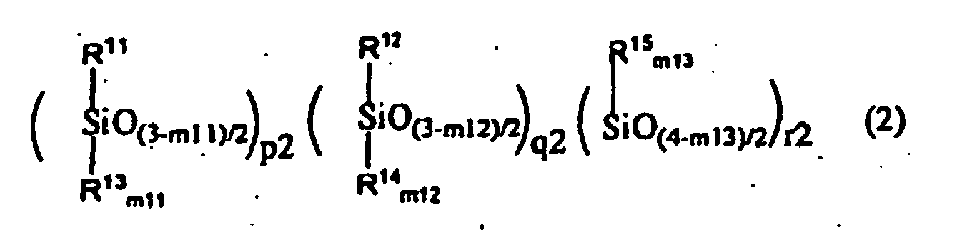
an organic solvent; and
an acid generator. - The antireflection film composition according to Claim 1 or Claim 2, wherein the chelating agent is selected from beta-diketones.
- The antireflection film composition according to Claim 1 or Claim 3, wherein R2 in the general formula (1) has a phenyl group.
- The antireflection film composition according to Claim 2 or Claim 3, wherein R12 in the general formula (2) has a phenyl group.
- A patterning process for patterning a substrate with lithography comprising: at least
forming an organic film (23) over a substrate (22) as a lower resist film;
applying the antireflection film composition according to any one of Claims 1 to 5 over the lower resist film, and baking the composition to form an antireflection film (20) as an intermediate resist film;
applying a photoresist film composition over the intermediate resist film, and prebaking the composition to form a photoresist film (21) as an upper resist film;
exposing a pattern circuit area of the upper resist film and then developing the film with a developer to form a resist pattern on the upper resist film;
etching the intermediate resist film with using the upper resist film on which the resist pattern is formed as a mask;
etching the lower resist film with using the patterned intermediate resist film as a mask; and
etching the substrate (22) with using the lower resist film as a mask. - The patterning process according to Claim 6, wherein a process layer (22a) of the substrate (22) to be patterned is a low dielectric constant film having a dielectric constant of 3.8 or less.
- The patterning process according to Claim 6 or Claim 7, wherein the intermediate resist film is removed with wet stripping after being patterned.
- A multilayer resist element comprising at least an organic film (23), an antireflection film (20) over the organic film (23), and a photoresist film (21) over the antireflection film (20), wherein the antireflection film (20) is formed by applying the antireflection film composition according to any one of Claims 1 to 5 over the organic film (23), and baking the composition,
Applications Claiming Priority (1)
| Application Number | Priority Date | Filing Date | Title |
|---|---|---|---|
| JP2005360202A JP4553835B2 (en) | 2005-12-14 | 2005-12-14 | Antireflection film material, pattern forming method using the same, and substrate |
Publications (2)
| Publication Number | Publication Date |
|---|---|
| EP1798599A1 EP1798599A1 (en) | 2007-06-20 |
| EP1798599B1 true EP1798599B1 (en) | 2008-08-06 |
Family
ID=37897314
Family Applications (1)
| Application Number | Title | Priority Date | Filing Date |
|---|---|---|---|
| EP06025581A Not-in-force EP1798599B1 (en) | 2005-12-14 | 2006-12-11 | Antireflection film composition, patterning process and substrate using the same |
Country Status (6)
| Country | Link |
|---|---|
| US (1) | US20070134916A1 (en) |
| EP (1) | EP1798599B1 (en) |
| JP (1) | JP4553835B2 (en) |
| KR (1) | KR101319233B1 (en) |
| DE (1) | DE602006002095D1 (en) |
| TW (1) | TWI346253B (en) |
Families Citing this family (61)
| Publication number | Priority date | Publication date | Assignee | Title |
|---|---|---|---|---|
| WO2004030049A2 (en) * | 2002-09-27 | 2004-04-08 | Tokyo Electron Limited | A method and system for etching high-k dielectric materials |
| FR2915832B1 (en) * | 2007-05-04 | 2009-07-03 | Commissariat Energie Atomique | METHOD OF MANUFACTURING PATTERNS WITHIN A POLYMER LAYER |
| JP4716044B2 (en) * | 2007-07-04 | 2011-07-06 | 信越化学工業株式会社 | Silicon-containing film forming composition, silicon-containing film, silicon-containing film-forming substrate, and pattern forming method using the same |
| JP4716045B2 (en) * | 2007-07-04 | 2011-07-06 | 信越化学工業株式会社 | Silicon-containing film forming composition, silicon-containing film, silicon-containing film-forming substrate, and pattern forming method using the same |
| US8652750B2 (en) * | 2007-07-04 | 2014-02-18 | Shin-Etsu Chemical Co., Ltd. | Silicon-containing film-forming composition, silicon-containing film, silicon-containing film-bearing substrate, and patterning method |
| CN101526737B (en) * | 2007-11-05 | 2014-02-26 | 罗门哈斯电子材料有限公司 | Composition for dip lithography and dip lithography method |
| JP4793592B2 (en) | 2007-11-22 | 2011-10-12 | 信越化学工業株式会社 | Metal oxide-containing film forming composition, metal oxide-containing film, metal oxide-containing film-forming substrate, and pattern forming method using the same |
| JP5433152B2 (en) * | 2008-01-18 | 2014-03-05 | 東京応化工業株式会社 | Film-forming composition for room temperature imprint, structure manufacturing method and structure |
| US11392037B2 (en) | 2008-02-18 | 2022-07-19 | Nissan Chemical Industries, Ltd. | Resist underlayer film forming composition containing silicone having cyclic amino group |
| JP2009204674A (en) * | 2008-02-26 | 2009-09-10 | Toshiba Corp | Pattern forming method |
| CN102124064B (en) | 2008-08-18 | 2014-09-03 | 日产化学工业株式会社 | Composition for forming silicon-containing resist underlayer film with onium group |
| JP5015892B2 (en) | 2008-10-02 | 2012-08-29 | 信越化学工業株式会社 | Silicon-containing film-forming composition, silicon-containing film-forming substrate, and pattern forming method |
| JP5015891B2 (en) * | 2008-10-02 | 2012-08-29 | 信越化学工業株式会社 | Metal oxide-containing film forming composition, metal oxide-containing film forming substrate, and pattern forming method |
| JP4813537B2 (en) | 2008-11-07 | 2011-11-09 | 信越化学工業株式会社 | Resist underlayer material containing thermal acid generator, resist underlayer film forming substrate, and pattern forming method |
| JP4790786B2 (en) * | 2008-12-11 | 2011-10-12 | 信越化学工業株式会社 | Method for peeling coating-type silicon-containing film |
| KR101288572B1 (en) * | 2008-12-17 | 2013-07-22 | 제일모직주식회사 | Hardmask Composition Coated under Photoresist with Improved Storage Stability |
| WO2010071155A1 (en) | 2008-12-19 | 2010-06-24 | 日産化学工業株式会社 | Silicon-containing resist underlayer film formation composition having anion group |
| JP4826840B2 (en) | 2009-01-15 | 2011-11-30 | 信越化学工業株式会社 | Pattern formation method |
| JP4826841B2 (en) | 2009-01-15 | 2011-11-30 | 信越化学工業株式会社 | Pattern formation method |
| JP4826846B2 (en) | 2009-02-12 | 2011-11-30 | 信越化学工業株式会社 | Pattern formation method |
| JP5618095B2 (en) | 2009-06-02 | 2014-11-05 | 日産化学工業株式会社 | Silicon-containing resist underlayer film forming composition having sulfide bond |
| CN102439523B (en) * | 2009-07-23 | 2015-01-07 | 道康宁公司 | Method and materials for double patterning |
| KR101749601B1 (en) | 2009-09-16 | 2017-06-21 | 닛산 가가쿠 고교 가부시키 가이샤 | Silicon-containing composition having sulfonamide group for forming resist underlayer film |
| US8288271B2 (en) * | 2009-11-02 | 2012-10-16 | International Business Machines Corporation | Method for reworking antireflective coating over semiconductor substrate |
| KR101947105B1 (en) | 2010-02-19 | 2019-02-13 | 닛산 가가쿠 가부시키가이샤 | Composition for formation of resist underlayer film containing silicon having nitrogen-containing ring |
| JP2011181123A (en) * | 2010-02-26 | 2011-09-15 | Fuji Electric Device Technology Co Ltd | Method of manufacturing magnetic recording medium |
| IL213195A0 (en) | 2010-05-31 | 2011-07-31 | Rohm & Haas Elect Mat | Photoresist compositions and emthods of forming photolithographic patterns |
| JP5229278B2 (en) | 2010-06-21 | 2013-07-03 | 信越化学工業株式会社 | Naphthalene derivative, resist underlayer film material, resist underlayer film forming method and pattern forming method |
| JP5556773B2 (en) | 2010-09-10 | 2014-07-23 | 信越化学工業株式会社 | Naphthalene derivative and method for producing the same, resist underlayer film material, resist underlayer film forming method and pattern forming method |
| US8568958B2 (en) * | 2011-06-21 | 2013-10-29 | Az Electronic Materials Usa Corp. | Underlayer composition and process thereof |
| JP5650086B2 (en) * | 2011-06-28 | 2015-01-07 | 信越化学工業株式会社 | Resist underlayer film forming composition and pattern forming method |
| JP5999372B2 (en) * | 2011-07-20 | 2016-09-28 | 日産化学工業株式会社 | Thin film forming composition for lithography containing titanium and silicon |
| JP5889568B2 (en) | 2011-08-11 | 2016-03-22 | メルク、パテント、ゲゼルシャフト、ミット、ベシュレンクテル、ハフツングMerck Patent GmbH | Composition for forming tungsten oxide film and method for producing tungsten oxide film using the same |
| JP5653880B2 (en) | 2011-10-11 | 2015-01-14 | 信越化学工業株式会社 | Resist underlayer film forming material and pattern forming method |
| JP5882776B2 (en) | 2012-02-14 | 2016-03-09 | 信越化学工業株式会社 | Resist underlayer film forming composition and pattern forming method |
| JP5739360B2 (en) | 2012-02-14 | 2015-06-24 | 信越化学工業株式会社 | Silicon-containing resist underlayer film forming composition and pattern forming method |
| TWI567497B (en) * | 2012-04-06 | 2017-01-21 | Az電子材料盧森堡有限公司 | Negative-type photosensitive siloxane composition |
| GB201211309D0 (en) | 2012-06-26 | 2012-08-08 | Fujifilm Mfg Europe Bv | Process for preparing membranes |
| US9315636B2 (en) | 2012-12-07 | 2016-04-19 | Az Electronic Materials (Luxembourg) S.A.R.L. | Stable metal compounds, their compositions and methods |
| JP5756134B2 (en) | 2013-01-08 | 2015-07-29 | 信越化学工業株式会社 | Metal oxide-containing film forming composition and pattern forming method |
| JP5842841B2 (en) | 2013-02-18 | 2016-01-13 | 信越化学工業株式会社 | Pattern formation method |
| JP5794243B2 (en) | 2013-02-18 | 2015-10-14 | 信越化学工業株式会社 | Pattern formation method |
| US9201305B2 (en) | 2013-06-28 | 2015-12-01 | Az Electronic Materials (Luxembourg) S.A.R.L. | Spin-on compositions of soluble metal oxide carboxylates and methods of their use |
| US9296922B2 (en) | 2013-08-30 | 2016-03-29 | Az Electronic Materials (Luxembourg) S.A.R.L. | Stable metal compounds as hardmasks and filling materials, their compositions and methods of use |
| US9409793B2 (en) | 2014-01-14 | 2016-08-09 | Az Electronic Materials (Luxembourg) S.A.R.L. | Spin coatable metallic hard mask compositions and processes thereof |
| JP2015199916A (en) * | 2014-04-02 | 2015-11-12 | Jsr株式会社 | Film-forming composition and pattern-forming method |
| TWI548429B (en) | 2014-11-07 | 2016-09-11 | 財團法人工業技術研究院 | Medical composite material method for fabricating the same and applications thereof |
| JP6660023B2 (en) | 2014-11-19 | 2020-03-04 | 日産化学株式会社 | Silicon-containing resist underlayer film forming composition capable of wet removal |
| TWI522231B (en) | 2014-12-01 | 2016-02-21 | 財團法人工業技術研究院 | Metal/polymer composite material and method for fabricating the same |
| TWI592760B (en) * | 2014-12-30 | 2017-07-21 | 羅門哈斯電子材料韓國有限公司 | Coating compositions for use with an overcoated photoresist |
| US9499698B2 (en) | 2015-02-11 | 2016-11-22 | Az Electronic Materials (Luxembourg)S.A.R.L. | Metal hardmask composition and processes for forming fine patterns on semiconductor substrates |
| TWI566036B (en) * | 2015-03-31 | 2017-01-11 | 奇美實業股份有限公司 | Photosensitive polysiloxane composition, protecting film, and element having the protecting film |
| JP2017097240A (en) * | 2015-11-26 | 2017-06-01 | Jsr株式会社 | Material for forming silicon-containing film and pattern formation method |
| JPWO2018079599A1 (en) | 2016-10-27 | 2019-09-19 | 日産化学株式会社 | Silicon-containing resist underlayer film forming composition containing organic group having dihydroxy group |
| JP6978594B2 (en) | 2017-09-06 | 2021-12-08 | メルク パテント ゲゼルシャフト ミット ベシュレンクテル ハフツングMerck Patent Gesellschaft mit beschraenkter Haftung | Spin-on inorganic oxide-containing composition useful as a hard mask and filling material with improved thermal stability |
| KR102053921B1 (en) * | 2019-03-13 | 2019-12-09 | 영창케미칼 주식회사 | New fine silicon etching pattern forming method in a semiconductor manufacturing process |
| WO2022210960A1 (en) | 2021-03-31 | 2022-10-06 | 日産化学株式会社 | Composition for forming silicon-containing underlayer film for induced self-organization |
| JPWO2022210954A1 (en) | 2021-03-31 | 2022-10-06 | ||
| TW202248296A (en) | 2021-03-31 | 2022-12-16 | 日商日產化學股份有限公司 | Composition for forming silicon-containing resist underlayer film |
| TW202336099A (en) | 2022-02-18 | 2023-09-16 | 日商日產化學股份有限公司 | Silicon-containing resist underlayer film forming composition having unsaturated bond and cyclic structure |
| CN116178723A (en) * | 2022-12-31 | 2023-05-30 | 江苏诚睿达光电有限公司 | Epoxy modified organic silicon resin and yellowing-resistant chip adhesive |
Family Cites Families (10)
| Publication number | Priority date | Publication date | Assignee | Title |
|---|---|---|---|---|
| US5294680A (en) * | 1992-07-24 | 1994-03-15 | International Business Machines Corporation | Polymeric dyes for antireflective coatings |
| US5328975A (en) * | 1993-04-02 | 1994-07-12 | Ppg Industries, Inc. | Ultraviolet radiation absorbing coating |
| JPH11258813A (en) * | 1998-03-13 | 1999-09-24 | Jsr Corp | Composition for forming antireflection film and antireflection film |
| US6268457B1 (en) * | 1999-06-10 | 2001-07-31 | Allied Signal, Inc. | Spin-on glass anti-reflective coatings for photolithography |
| US6420088B1 (en) * | 2000-06-23 | 2002-07-16 | International Business Machines Corporation | Antireflective silicon-containing compositions as hardmask layer |
| US6730454B2 (en) * | 2002-04-16 | 2004-05-04 | International Business Machines Corporation | Antireflective SiO-containing compositions for hardmask layer |
| JP4369203B2 (en) * | 2003-03-24 | 2009-11-18 | 信越化学工業株式会社 | Antireflection film material, substrate having antireflection film, and pattern forming method |
| US7303785B2 (en) * | 2003-06-03 | 2007-12-04 | Shin-Etsu Chemical Co., Ltd. | Antireflective film material, and antireflective film and pattern formation method using the same |
| JP2005173552A (en) * | 2003-11-20 | 2005-06-30 | Tokyo Ohka Kogyo Co Ltd | Undercoating layer forming material for lithography and wiring forming method using the same |
| JP4340167B2 (en) * | 2004-02-03 | 2009-10-07 | 信越化学工業株式会社 | Silicon-containing resist underlayer film material and pattern forming method |
-
2005
- 2005-12-14 JP JP2005360202A patent/JP4553835B2/en active Active
-
2006
- 2006-12-11 EP EP06025581A patent/EP1798599B1/en not_active Not-in-force
- 2006-12-11 US US11/636,647 patent/US20070134916A1/en not_active Abandoned
- 2006-12-11 DE DE602006002095T patent/DE602006002095D1/en active Active
- 2006-12-13 KR KR1020060127041A patent/KR101319233B1/en active IP Right Grant
- 2006-12-14 TW TW095146913A patent/TWI346253B/en not_active IP Right Cessation
Also Published As
| Publication number | Publication date |
|---|---|
| JP2007163846A (en) | 2007-06-28 |
| EP1798599A1 (en) | 2007-06-20 |
| DE602006002095D1 (en) | 2008-09-18 |
| TWI346253B (en) | 2011-08-01 |
| US20070134916A1 (en) | 2007-06-14 |
| TW200736839A (en) | 2007-10-01 |
| KR20070063440A (en) | 2007-06-19 |
| KR101319233B1 (en) | 2013-10-16 |
| JP4553835B2 (en) | 2010-09-29 |
Similar Documents
| Publication | Publication Date | Title |
|---|---|---|
| EP1798599B1 (en) | Antireflection film composition, patterning process and substrate using the same | |
| KR101097963B1 (en) | Antireflective film-forming composition, method for manufacturing the same, and antireflective film and pattern formation method using the same | |
| EP3039484B1 (en) | Stable metal compounds as hardmasks and filling materials, their compositions and methods of use | |
| JP4553113B2 (en) | Porous film-forming composition, pattern-forming method, and porous sacrificial film | |
| EP1813985B1 (en) | Antireflection film composition, substrate, and pattering process | |
| TWI669353B (en) | Metal hardmask composition and processes for forming fine patterns on semiconductor substrates | |
| KR101001399B1 (en) | Antireflection film material, substrate having antireflection film and pattern forming method | |
| KR101134190B1 (en) | Silicon-Containing Film Forming Compsition, Silicon-Containing Film Serving as Etching Mask, Substrate Processing Intermediate, and Substrate Processing Method | |
| US7736837B2 (en) | Antireflective coating composition based on silicon polymer | |
| US7638268B2 (en) | Rework process for photoresist film | |
| KR20090027249A (en) | Anti-reflective coating composition comprising siloxane polymer | |
| JP2005018054A (en) | Antireflection film material, antireflection film using the same and pattern forming method | |
| EP1801619B1 (en) | Substrate comprising two antireflective silicone resin layers between an organic layer and a photoresist layer, method for producing the same and patterning process using the same | |
| US7642043B2 (en) | Rework process for photoresist film |
Legal Events
| Date | Code | Title | Description |
|---|---|---|---|
| PUAI | Public reference made under article 153(3) epc to a published international application that has entered the european phase |
Free format text: ORIGINAL CODE: 0009012 |
|
| AK | Designated contracting states |
Kind code of ref document: A1 Designated state(s): AT BE BG CH CY CZ DE DK EE ES FI FR GB GR HU IE IS IT LI LT LU LV MC NL PL PT RO SE SI SK TR |
|
| AX | Request for extension of the european patent |
Extension state: AL BA HR MK YU |
|
| RAP1 | Party data changed (applicant data changed or rights of an application transferred) |
Owner name: SHIN-ETSU CHEMICAL CO., LTD. |
|
| 17P | Request for examination filed |
Effective date: 20070913 |
|
| GRAP | Despatch of communication of intention to grant a patent |
Free format text: ORIGINAL CODE: EPIDOSNIGR1 |
|
| AKX | Designation fees paid |
Designated state(s): DE FR GB |
|
| GRAS | Grant fee paid |
Free format text: ORIGINAL CODE: EPIDOSNIGR3 |
|
| GRAA | (expected) grant |
Free format text: ORIGINAL CODE: 0009210 |
|
| AK | Designated contracting states |
Kind code of ref document: B1 Designated state(s): DE FR GB |
|
| REG | Reference to a national code |
Ref country code: GB Ref legal event code: FG4D |
|
| REF | Corresponds to: |
Ref document number: 602006002095 Country of ref document: DE Date of ref document: 20080918 Kind code of ref document: P |
|
| PLBE | No opposition filed within time limit |
Free format text: ORIGINAL CODE: 0009261 |
|
| STAA | Information on the status of an ep patent application or granted ep patent |
Free format text: STATUS: NO OPPOSITION FILED WITHIN TIME LIMIT |
|
| 26N | No opposition filed |
Effective date: 20090507 |
|
| REG | Reference to a national code |
Ref country code: FR Ref legal event code: PLFP Year of fee payment: 10 |
|
| PGFP | Annual fee paid to national office [announced via postgrant information from national office to epo] |
Ref country code: GB Payment date: 20151209 Year of fee payment: 10 |
|
| PGFP | Annual fee paid to national office [announced via postgrant information from national office to epo] |
Ref country code: FR Payment date: 20151110 Year of fee payment: 10 |
|
| GBPC | Gb: european patent ceased through non-payment of renewal fee |
Effective date: 20161211 |
|
| REG | Reference to a national code |
Ref country code: FR Ref legal event code: ST Effective date: 20170831 |
|
| PG25 | Lapsed in a contracting state [announced via postgrant information from national office to epo] |
Ref country code: FR Free format text: LAPSE BECAUSE OF NON-PAYMENT OF DUE FEES Effective date: 20170102 |
|
| PG25 | Lapsed in a contracting state [announced via postgrant information from national office to epo] |
Ref country code: GB Free format text: LAPSE BECAUSE OF NON-PAYMENT OF DUE FEES Effective date: 20161211 |
|
| PGFP | Annual fee paid to national office [announced via postgrant information from national office to epo] |
Ref country code: DE Payment date: 20191126 Year of fee payment: 14 |
|
| REG | Reference to a national code |
Ref country code: DE Ref legal event code: R119 Ref document number: 602006002095 Country of ref document: DE |
|
| PG25 | Lapsed in a contracting state [announced via postgrant information from national office to epo] |
Ref country code: DE Free format text: LAPSE BECAUSE OF NON-PAYMENT OF DUE FEES Effective date: 20210701 |