EP1713055A1 - Luminance adjustment method, liquid crystal display device, and computer program - Google Patents
Luminance adjustment method, liquid crystal display device, and computer program Download PDFInfo
- Publication number
- EP1713055A1 EP1713055A1 EP04818935A EP04818935A EP1713055A1 EP 1713055 A1 EP1713055 A1 EP 1713055A1 EP 04818935 A EP04818935 A EP 04818935A EP 04818935 A EP04818935 A EP 04818935A EP 1713055 A1 EP1713055 A1 EP 1713055A1
- Authority
- EP
- European Patent Office
- Prior art keywords
- luminance
- liquid crystal
- crystal panel
- level
- backlight
- Prior art date
- Legal status (The legal status is an assumption and is not a legal conclusion. Google has not performed a legal analysis and makes no representation as to the accuracy of the status listed.)
- Granted
Links
Images


Classifications
-
- G—PHYSICS
- G09—EDUCATION; CRYPTOGRAPHY; DISPLAY; ADVERTISING; SEALS
- G09G—ARRANGEMENTS OR CIRCUITS FOR CONTROL OF INDICATING DEVICES USING STATIC MEANS TO PRESENT VARIABLE INFORMATION
- G09G3/00—Control arrangements or circuits, of interest only in connection with visual indicators other than cathode-ray tubes
- G09G3/20—Control arrangements or circuits, of interest only in connection with visual indicators other than cathode-ray tubes for presentation of an assembly of a number of characters, e.g. a page, by composing the assembly by combination of individual elements arranged in a matrix no fixed position being assigned to or needed to be assigned to the individual characters or partial characters
- G09G3/34—Control arrangements or circuits, of interest only in connection with visual indicators other than cathode-ray tubes for presentation of an assembly of a number of characters, e.g. a page, by composing the assembly by combination of individual elements arranged in a matrix no fixed position being assigned to or needed to be assigned to the individual characters or partial characters by control of light from an independent source
- G09G3/36—Control arrangements or circuits, of interest only in connection with visual indicators other than cathode-ray tubes for presentation of an assembly of a number of characters, e.g. a page, by composing the assembly by combination of individual elements arranged in a matrix no fixed position being assigned to or needed to be assigned to the individual characters or partial characters by control of light from an independent source using liquid crystals
- G09G3/3611—Control of matrices with row and column drivers
-
- G—PHYSICS
- G02—OPTICS
- G02F—OPTICAL DEVICES OR ARRANGEMENTS FOR THE CONTROL OF LIGHT BY MODIFICATION OF THE OPTICAL PROPERTIES OF THE MEDIA OF THE ELEMENTS INVOLVED THEREIN; NON-LINEAR OPTICS; FREQUENCY-CHANGING OF LIGHT; OPTICAL LOGIC ELEMENTS; OPTICAL ANALOGUE/DIGITAL CONVERTERS
- G02F1/00—Devices or arrangements for the control of the intensity, colour, phase, polarisation or direction of light arriving from an independent light source, e.g. switching, gating or modulating; Non-linear optics
- G02F1/01—Devices or arrangements for the control of the intensity, colour, phase, polarisation or direction of light arriving from an independent light source, e.g. switching, gating or modulating; Non-linear optics for the control of the intensity, phase, polarisation or colour
- G02F1/13—Devices or arrangements for the control of the intensity, colour, phase, polarisation or direction of light arriving from an independent light source, e.g. switching, gating or modulating; Non-linear optics for the control of the intensity, phase, polarisation or colour based on liquid crystals, e.g. single liquid crystal display cells
- G02F1/133—Constructional arrangements; Operation of liquid crystal cells; Circuit arrangements
- G02F1/1333—Constructional arrangements; Manufacturing methods
- G02F1/1335—Structural association of cells with optical devices, e.g. polarisers or reflectors
-
- G—PHYSICS
- G09—EDUCATION; CRYPTOGRAPHY; DISPLAY; ADVERTISING; SEALS
- G09G—ARRANGEMENTS OR CIRCUITS FOR CONTROL OF INDICATING DEVICES USING STATIC MEANS TO PRESENT VARIABLE INFORMATION
- G09G3/00—Control arrangements or circuits, of interest only in connection with visual indicators other than cathode-ray tubes
- G09G3/20—Control arrangements or circuits, of interest only in connection with visual indicators other than cathode-ray tubes for presentation of an assembly of a number of characters, e.g. a page, by composing the assembly by combination of individual elements arranged in a matrix no fixed position being assigned to or needed to be assigned to the individual characters or partial characters
- G09G3/34—Control arrangements or circuits, of interest only in connection with visual indicators other than cathode-ray tubes for presentation of an assembly of a number of characters, e.g. a page, by composing the assembly by combination of individual elements arranged in a matrix no fixed position being assigned to or needed to be assigned to the individual characters or partial characters by control of light from an independent source
- G09G3/3406—Control of illumination source
-
- G—PHYSICS
- G09—EDUCATION; CRYPTOGRAPHY; DISPLAY; ADVERTISING; SEALS
- G09G—ARRANGEMENTS OR CIRCUITS FOR CONTROL OF INDICATING DEVICES USING STATIC MEANS TO PRESENT VARIABLE INFORMATION
- G09G3/00—Control arrangements or circuits, of interest only in connection with visual indicators other than cathode-ray tubes
- G09G3/20—Control arrangements or circuits, of interest only in connection with visual indicators other than cathode-ray tubes for presentation of an assembly of a number of characters, e.g. a page, by composing the assembly by combination of individual elements arranged in a matrix no fixed position being assigned to or needed to be assigned to the individual characters or partial characters
- G09G3/34—Control arrangements or circuits, of interest only in connection with visual indicators other than cathode-ray tubes for presentation of an assembly of a number of characters, e.g. a page, by composing the assembly by combination of individual elements arranged in a matrix no fixed position being assigned to or needed to be assigned to the individual characters or partial characters by control of light from an independent source
- G09G3/36—Control arrangements or circuits, of interest only in connection with visual indicators other than cathode-ray tubes for presentation of an assembly of a number of characters, e.g. a page, by composing the assembly by combination of individual elements arranged in a matrix no fixed position being assigned to or needed to be assigned to the individual characters or partial characters by control of light from an independent source using liquid crystals
- G09G3/3607—Control arrangements or circuits, of interest only in connection with visual indicators other than cathode-ray tubes for presentation of an assembly of a number of characters, e.g. a page, by composing the assembly by combination of individual elements arranged in a matrix no fixed position being assigned to or needed to be assigned to the individual characters or partial characters by control of light from an independent source using liquid crystals for displaying colours or for displaying grey scales with a specific pixel layout, e.g. using sub-pixels
-
- G—PHYSICS
- G09—EDUCATION; CRYPTOGRAPHY; DISPLAY; ADVERTISING; SEALS
- G09G—ARRANGEMENTS OR CIRCUITS FOR CONTROL OF INDICATING DEVICES USING STATIC MEANS TO PRESENT VARIABLE INFORMATION
- G09G2320/00—Control of display operating conditions
- G09G2320/06—Adjustment of display parameters
- G09G2320/0606—Manual adjustment
-
- G—PHYSICS
- G09—EDUCATION; CRYPTOGRAPHY; DISPLAY; ADVERTISING; SEALS
- G09G—ARRANGEMENTS OR CIRCUITS FOR CONTROL OF INDICATING DEVICES USING STATIC MEANS TO PRESENT VARIABLE INFORMATION
- G09G2320/00—Control of display operating conditions
- G09G2320/06—Adjustment of display parameters
- G09G2320/0626—Adjustment of display parameters for control of overall brightness
-
- G—PHYSICS
- G09—EDUCATION; CRYPTOGRAPHY; DISPLAY; ADVERTISING; SEALS
- G09G—ARRANGEMENTS OR CIRCUITS FOR CONTROL OF INDICATING DEVICES USING STATIC MEANS TO PRESENT VARIABLE INFORMATION
- G09G2320/00—Control of display operating conditions
- G09G2320/06—Adjustment of display parameters
- G09G2320/0666—Adjustment of display parameters for control of colour parameters, e.g. colour temperature
-
- G—PHYSICS
- G09—EDUCATION; CRYPTOGRAPHY; DISPLAY; ADVERTISING; SEALS
- G09G—ARRANGEMENTS OR CIRCUITS FOR CONTROL OF INDICATING DEVICES USING STATIC MEANS TO PRESENT VARIABLE INFORMATION
- G09G2320/00—Control of display operating conditions
- G09G2320/06—Adjustment of display parameters
- G09G2320/0673—Adjustment of display parameters for control of gamma adjustment, e.g. selecting another gamma curve
-
- G—PHYSICS
- G09—EDUCATION; CRYPTOGRAPHY; DISPLAY; ADVERTISING; SEALS
- G09G—ARRANGEMENTS OR CIRCUITS FOR CONTROL OF INDICATING DEVICES USING STATIC MEANS TO PRESENT VARIABLE INFORMATION
- G09G2320/00—Control of display operating conditions
- G09G2320/06—Adjustment of display parameters
- G09G2320/0693—Calibration of display systems
-
- G—PHYSICS
- G09—EDUCATION; CRYPTOGRAPHY; DISPLAY; ADVERTISING; SEALS
- G09G—ARRANGEMENTS OR CIRCUITS FOR CONTROL OF INDICATING DEVICES USING STATIC MEANS TO PRESENT VARIABLE INFORMATION
- G09G2360/00—Aspects of the architecture of display systems
- G09G2360/14—Detecting light within display terminals, e.g. using a single or a plurality of photosensors
- G09G2360/145—Detecting light within display terminals, e.g. using a single or a plurality of photosensors the light originating from the display screen
Definitions
- the present invention relates to: a luminance control method for a liquid crystal display device comprising a liquid crystal panel and a backlight disposed at the back of the liquid crystal panel; a liquid crystal display device to which the luminance control method is applied; and a computer program for realizing the luminance control method with a computer.
- a liquid crystal display device displays an image by controlling On/Off of each pixel in a liquid crystal panel on the basis of a video signal inputted from a personal computer (which will be hereinafter referred to as a PC) or the like and by applying to each pixel a data voltage according to the video signal with a built-in gate driver and a built-in source driver so as to control light transmittance determined by an electrooptical characteristic of a liquid crystal material.
- a personal computer which will be hereinafter referred to as a PC
- a built-in gate driver and a built-in source driver so as to control light transmittance determined by an electrooptical characteristic of a liquid crystal material.
- FIG. 13 is a graph showing an example of the electrooptical characteristic of a liquid crystal material, wherein the abscissa axis denotes the voltage applied to the liquid crystal material while the ordinate axis denotes the light transmittance of the liquid crystal material.
- a continuous line B denotes a characteristic obtained when the liquid crystal gap d satisfies d ⁇ 3/(2 ⁇ n)
- a continuous line C denotes a characteristic obtained when the liquid crystal gap d satisfies d> ⁇ 3/(2 ⁇ n)
- the liquid crystal gap d which is a parameter for determining the light transmittance of a liquid crystal display device, might be narrower or wider than a designed value due to a variation in manufacture, causing a problem that a desired light transmittance cannot be obtained and an intended gray-level display cannot be provided.
- a liquid crystal display device comprising a memory for storing a look-up table (which will be hereinafter referred to as an LUT) in which a gray level represented by the inputted video signal is associated with an input level to a liquid crystal panel corresponding to the gray level, whereby a desired gray-level characteristic can be realized by converting a gray level into an input level on the basis of the LUT and correcting specific characteristics of the device (see, for example, Patent Document 1).
- a look-up table which will be hereinafter referred to as an LUT
- a gray level represented by the inputted video signal is associated with an input level to a liquid crystal panel corresponding to the gray level
- the liquid crystal display device disclosed in the Patent Document 1 measures a luminance in each input level with an external photosensor (luminance meter) provided at the front of the liquid crystal panel and evaluates an actual panel gray-level characteristic of the liquid crystal panel.
- a gray level and an input level, which are to be written into the LUT, are calculated from the measured panel gray-level characteristic and the desired ideal gray-level characteristic, and stored in the LUT.
- FIG. 14 is a concept view showing an example of the content of the LUT.
- the LUT stores a gray level as an index associated with an input level as a value. It should be noted that shown is an example wherein the number of gray levels is 8 bits (256) and the input level is 10 bits (1024), i.e. 2 bits larger than the number of gray levels.
- the LUT stores a gray level "0" associated with an input level "0", a gray level "1” associated with an input level "5", a gray level "2" associated with an input level "8", ..., and a gray level "255" associated with an input level "1023".
- the liquid crystal display device converts an inputted gray level (FIG. 15(a)) of each pixel into an input level (FIG. 15(b)) associated with the gray level on the basis of the LUT, and outputs it.
- FIG. 16 is an explanatory view showing the concept of luminance control using the LUT.
- the continuous line denotes an actual gray-level characteristic of the liquid crystal panel and the broken line denotes an ideal gray-level characteristic to be set.
- the liquid crystal display device converts a gray level X represented by the inputted video signal into an input level Y to the liquid crystal panel on the basis of the LUT to obtain a luminance Q, which gives an ideal gray-level characteristic, so as to realize an ideal gray-level characteristic artificially.
- Patent Document 1 Japanese Patent Application Laid-Open No.2002-99238
- Ideal gray-level characteristics are divided into two groups: one changes relatively to the maximum luminance, and the other one does not change relatively to the maximum luminance.
- a specific example of the former is a gamma characteristic, and a specific example of the latter is the gray-scale display function (which will be hereinafter referred to as the GSDF) compatible with the DICOM (standard for a medical imaging device).
- the GSDF gray-scale display function
- the continuous line denotes a characteristic obtained when the luminance at 255-gray level (maximum luminance) is 600cd/m 2 and the luminance at 0-gray level (minimum luminance) is 1cd/m 2
- the broken line denotes a characteristic obtained when the maximum luminance is 300cd/m 2 and the minimum luminance is 1cd/m 2 .
- the gamma characteristic is represented by a per se known expression (2).
- FIG. 19 is a graph showing the GSDF compatible with the DICOM, wherein the abscissa axis denotes the gray level and the ordinate axis denotes the luminance.
- the continuous line denotes a characteristic obtained when the maximum luminance is 600cd/m 2 and the minimum luminance is 1cd/m 2
- the broken line denotes a characteristic obtained when the maximum luminance is 300cd/m 2 and the minimum luminance is 1cd/m 2 .
- each GSDF when normalized by the maximum luminance, has a different characteristic (curve) according to the maximum luminance, differently from the above gamma characteristic.
- a gray level which gives the same normalized luminance Q is a gray level Y (203) when the maximum luminance is 600cd/m 2
- the gray level thus differs (X ⁇ Y). Accordingly, there arises a need to change the LUT when the ideal gray-level characteristic does not change relatively to the maximum luminance.
- the liquid crystal display device which is not a selfluminous display device, needs a backlight as a light source and the luminance of the backlight generally changes as the backlight is used.
- aspects of the change in the luminance of the backlight include a fact that time (aging time) is required until the luminance is stabilized and a fact that the luminance gradually decreases depending on cumulative operating time.
- the luminance of a conventional liquid crystal display device can be controlled, controlled is only the brightness, i.e. the ratio of luminance, so that a user cannot evaluate the luminance value during control (e.g. brightness 50%) and has to rely on his own sensitivity. That is, the brightness can be controlled only qualitatively, and there is no liquid crystal display device capable of controlling the luminance as desired, although it is desirable to control the luminance quantitatively according to conditions such as user preference, use environment and the type of a screen image to be displayed.
- the present invention has been made with the aim of solving the above problems, and it is an object thereof to provide a luminance control method for a liquid crystal display device capable of controlling a luminance of a backlight and setting the luminance quantitatively by uniquely obtaining the relation between the luminance of the backlight and a luminance of light emitted from the backlight through a liquid crystal panel and by uniquely calculating the luminance of light emitted from the backlight through the liquid crystal panel on the basis of the luminance of the backlight.
- Another object of the present invention is to provide a luminance control method for a liquid crystal display device capable of realizing a superior gray-level characteristic by obtaining an actual gray-level characteristic of a liquid crystal panel, by calculating a luminance to be set, i.e. a desired ideal gray-level characteristic, and by comparing both the gray-level characteristics to control the luminance.
- Still further object of the present invention is to provide a liquid crystal display device to which the luminance control method is applied and a computer program for realizing the luminance control method with a computer.
- a luminance control method is a luminance control method for a liquid crystal display device, which comprises a liquid crystal display panel and a backlight disposed at the back of the liquid crystal panel, for controlling an input level of a video signal to be inputted into the liquid crystal panel to control the transmittance of the liquid crystal panel and provide a gray-level display
- the liquid crystal display device further comprises luminance detecting means for detecting a luminance of the backlight
- the method comprises the steps of: measuring a luminance of light emitted from the backlight through the liquid crystal panel in a plurality of states where the liquid crystal panel has a predetermined transmittance and the backlight has a different luminance, and preliminarily storing the luminance measured in each state associated with the luminance detected by the luminance detecting means; setting a desired luminance set value of light emitted through the liquid crystal panel in a state where the liquid crystal panel has a predetermined transmittance; calculating a luminance to be detected by the luminance
- a luminance control method further comprises the steps of: measuring a luminance of light emitted through the liquid crystal panel in each input level, and preliminarily storing the measured luminance associated with an input level which gives the luminance; calculating a luminance of light emitted through the liquid crystal panel in each input level and a luminance to be set in each gray level in a case of the luminance set value on the basis of the stored luminance and input level; extracting an input level which gives a luminance substantially equal to the luminance to be set in each gray level on the basis of the luminance in each calculated input level and the luminance to be set in each gray level, and storing the extracted input level associated with a gray level; and controlling the transmittance of the liquid crystal panel in a gray level associated with the input level of the video signal.
- a luminance control method further comprises the steps of: measuring a luminance of light emitted through the liquid crystal panel in each input level; normalizing each measured luminance, and preliminarily storing each normalized luminance associated with an input level which gives the luminance; calculating a luminance of light emitted through the liquid crystal panel in each input level and a luminance to be set in each gray level in a case of the luminance set value on the basis of the stored luminance and input level; extracting an input level which gives a luminance substantially equal to the luminance to be set in each gray level on the basis of the luminance in each calculated input level and the luminance to be set in each gray level, and storing the extracted input level associated with a gray level; and controlling the transmittance of the liquid crystal panel in a gray level associated with the input level of the video signal.
- the luminance set value is a luminance in a state where the transmittance of the liquid crystal panel is a controllable maximum transmittance.
- one state of the plurality of states is a state where the backlight has a controllable maximum luminance and another state of the plurality of states is a state where the backlight has a controllable minimum luminance.
- a liquid crystal display device is a liquid crystal display device, which comprises a liquid crystal panel and a backlight disposed at the back of the liquid crystal panel, for controlling an input level of a video signal to be inputted to the liquid crystal panel to control the transmittance of the liquid crystal panel and provide a gray-level display, further comprising: luminance detecting means for detecting a luminance of the backlight; a storage unit for preliminarily storing information in which the luminance detected by the luminance detecting means in a plurality of states where the liquid crystal panel has a predetermined transmittance and the backlight has a different luminance is associated with a luminance of light emitted from the backlight through the liquid crystal panel; accepting means for accepting a desired luminance set value of light emitted through the liquid crystal panel in a state where the liquid crystal panel has a predetermined transmittance; calculating means for calculating a luminance to be detected by the luminance detecting means, which is to be the luminance set value accepted by the
- the storage unit further stores second information on a luminance of light emitted through the liquid crystal panel in each input level
- the device further comprises: second calculating means for calculating a luminance of light emitted through the liquid crystal panel in each input level in a case of the luminance set value accepted by the accepting means on the basis of the second information; third calculating means for calculating a luminance to be set in each gray level in a case of the luminance set value accepted by the accepting means; fourth calculating means for calculating a luminance difference between the luminance to be set in each gray level calculated by the third calculating means and the luminance in each input level calculated by the second calculating means; storage means for storing an input level, which gives a minimum luminance difference calculated by the fourth calculating means, associated with a gray level; and control means for controlling the transmittance of the liquid crystal panel in a gray level associated with the input level of the video signal.
- the luminance detecting means has: photoelectric conversion means for converting the luminance of the backlight into an analog-type electric signal having a voltage corresponding to the luminance of the backlight; and analog-digital conversion means for converting the converted analog-type electric signal into a digital-type electric signal.
- a computer program is a computer program for causing a computer to output control information to a liquid crystal display device comprising a liquid crystal panel and a backlight disposed at the back of the liquid crystal panel and causing the computer to control an input level of a video signal to be inputted into the liquid crystal panel to control the transmittance of the liquid crystal panel and provide a gray-level display, comprising the steps of: causing the computer to store in a storage unit a luminance of the backlight, in a plurality of states where the backlight has a different luminance, associated with a luminance of light emitted from the backlight through the liquid crystal panel; causing the computer to set a desired luminance set value of light emitted through the liquid crystal panel; causing the computer to calculate control information for controlling a luminance of the backlight, which is to be the set luminance set value, on the basis of information stored in the storage unit; and causing the computer to output the calculated control information to the liquid crystal display device.
- a computer program according to the tenth aspect of the present invention, as set forth in the ninth aspect, further comprises the steps of: causing the computer to store in a storage unit second information on a luminance of light emitted through the liquid crystal panel in each input level; causing the computer to calculate a luminance of light emitted through the liquid crystal panel in each input level in a case of the inputted luminance set value on the basis of the stored second information; causing the computer to calculate a luminance to be set in each gray level in a case of the inputted luminance set value; causing the computer to calculate a luminance difference between the calculated luminance to be set in each gray level and the calculated luminance in each input level; and causing the computer to store in the storage unit an input level, which gives a minimum calculated luminance difference, associated with a gray level.
- the luminance detected by the luminance detecting means and the luminance of light emitted from the backlight through the liquid crystal panel are measured in each of a plurality of states where the liquid crystal panel has a predetermined transmittance and the backlight has a different luminance, and both the luminances in each state are stored associated with each other. Since the relation between the luminance of the backlight and the luminance of light emitted from the backlight through the liquid crystal panel can be obtained uniquely, the luminance of light emitted from the backlight through the liquid crystal panel can be calculated based on the luminance of the backlight detected by the luminance detecting means.
- a desired luminance set value of light emitted through the liquid crystal panel is then set and the luminance of the backlight to be detected by the luminance detecting means in a case of the set luminance set value is calculated to control the luminance of the backlight. Accordingly, the luminance can be controlled so as to be a desired luminance set value, differently from conventional brightness control by which the luminance can be controlled only qualitatively.
- the luminance detected by the luminance detecting means and the luminance of light emitted from the backlight through the liquid crystal panel in a plurality of states where the backlight has a different luminance are measured in the production process of the liquid crystal display device and both the luminances in each state are preliminary stored associated with each other, there is no need to measure the luminance of light emitted through the liquid crystal panel using an external photosensor after shipment, the burden imposed on the user of the liquid crystal display device is decreased, highly accurate measurement is enabled as a series of processes, and it becomes possible to control the luminance so as to be a desired luminance with a high degree of accuracy.
- the invention can be utilized as a self-diagnosis function such as notification to the user of the present luminance or notification to the user of a fact that the luminance falls below a predetermined luminance, when it occurs.
- the luminance of light emitted through the liquid crystal panel in each input level is measured and the measured luminance is stored associated with an input level which gives the luminance.
- an actual gray-level characteristic of the liquid crystal panel can be obtained.
- the luminance of light emitted through the liquid crystal panel in each input level in a case where the luminance of light emitted through the liquid crystal panel is a luminance set value and the luminance (ideal luminance) to be set in each gray level is then calculated and an input level which gives a luminance substantially equal to the ideal luminance in each gray level is extracted. Since the input level can be set so as to give a luminance substantially equal to the ideal luminance in each gray level, it becomes possible to realize a superior gray-level characteristic.
- the luminance of light emitted through the liquid crystal panel in each input level is measured, each luminance of each measured input level is divided and normalized by the maximum luminance of the measured luminances, and each normalized luminance is stored associated with an input level which gives the luminance.
- each normalized luminance is stored associated with an input level which gives the luminance.
- the luminance of light emitted through the liquid crystal panel in each input level in a case where the luminance of light emitted through the liquid crystal panel is the luminance set value and a luminance (ideal luminance) to be set in each gray level is then calculated and an input level which gives a luminance substantially equal to the ideal luminance in each gray level is extracted. Since the input level can be set so as to give a luminance substantially equal to the ideal luminance in each gray level, it is possible to realize a superior gray-level characteristic.
- the input level for each wavelength band can be set individually so as to give a luminance substantially equal to the ideal luminance in each gray level. Since luminance control can be performed individually even when each wavelength band has a different gray-level characteristic, a superior gray-level characteristic can be realized.
- input level can be set individually for the three primary colors so as to give a luminance substantially equal to the ideal luminance in each gray level.
- the wavelength distribution of light emitted from the backlight might change generally due to aged deterioration, a gray-level characteristic having superior color reproducibility and superior white balance can be realized since luminance control can be performed individually for the three primary colors.
- the maximum luminance of light emitted through the liquid crystal panel can be set quantitatively.
- the relation between the luminance of the backlight and the luminance of light emitted from the backlight through the liquid crystal panel can be obtained with a high degree of accuracy.
- the luminance detecting means can be constructed at low cost using general-purpose photoelectric conversion means and analog-digital conversion means.
- the luminance of the backlight can be controlled and the luminance can be set quantitatively.
- a gray-level characteristic to be set can be calculated and both the gray-level characteristics are compared to control the luminance, and a superior gray-level characteristic can be realized.
- the present invention when the luminance of the backlight (luminance detected by the luminance detecting means) and the luminance of light emitted from the backlight through the liquid crystal panel are measured in the production process of the liquid crystal display device, since there is no need to measure the luminance of light emitted through the liquid crystal panel using an external photosensor after shipment, the burden imposed on the user of the liquid crystal display device is decreased, highly accurate measurement is enabled as a series of processes, and it becomes possible to control the luminance so as to be a desired luminance with a high degree of accuracy. Moreover, even when the gray-level characteristic does not change relatively to a change in the maximum luminance, a desired gray-level characteristic can be realized with a high degree of accuracy without using an external photosensor.
- FIG. 1 is a block diagram showing a structure example of a liquid crystal display device according to Embodiment 1 of the present invention.
- the liquid crystal display device 1 according to this embodiment comprises a control unit 2, a ROM 3, a RAM 4, an operation unit 5, a storage unit 6, a signal input unit 7, a liquid crystal drive circuit 8, a liquid crystal panel 9, a backlight power supply circuit 10, a backlight 11, a photosensor 12, and an ADC (A/D converter) 13.
- the liquid crystal display device 1 has a function of displaying a screen image on a display screen of the liquid crystal panel 9 on the basis of a video signal inputted through the signal input unit 7. Though the video signal might be of an analog type, the following description will explain a digital-type video signal.
- an external photosensor 22 is a device for measuring the luminance of light emitted through the liquid crystal panel 9, and is additionally used when the following first process procedure is performed.
- the control unit 2 which is specifically composed of a CPU connected with each hardware unit mentioned above through a bus 15, controls each hardware unit and performs a variety of software functions according to a control program stored in the ROM 3.
- the ROM 3 preliminarily stores a variety of software programs necessary for operations of the liquid crystal device as mentioned above.
- the operation unit 5 comprises various function keys for operating the liquid crystal display device 1.
- the function keys include a luminance control execution key 5a for setting whether a luminance control process is to be performed or not and a luminance setting key 5b for setting the luminance of the liquid crystal display device.
- an On Screen Display may be displayed on the liquid crystal panel 9 so as to operate various settings of the liquid crystal display device, or the liquid crystal panel 9 may be of a touch panel type so that a part of, or all of, various function keys of the operation unit 5 can be substituted.
- OSD On Screen Display
- the storage unit 6, which is a device rewritable as software, stores: an output value AD H of the ADC 13 and a luminance L MH of a substantially center part of the display surface of the liquid crystal panel 9 obtained when the brightness is the maximum (100%); an output value AD L of the ADC 13 and a luminance L ML of a substantially center part of the display surface of the liquid crystal panel obtained when the brightness is the minimum (0%); and luminance L 0 /L 1023 , L 1 /L 1023 , ..., L 1023 /L 1023 which is obtained by normalizing the luminance L 0 , L 1 , ..., L 1023 of a substantially center part of the display surface obtained when a source driver (mentioned later) outputs an output voltage for each input level (e.g.
- the storage unit 6 further has a function of timely updating and storing an LUT 6a in which a gray level is associated with an input level to the liquid crystal panel corresponding to the gray level.
- the content of the LUT 6a is the same as the conventional LUT illustrated in FIG. 14.
- the source driver 8b Supplied to the source driver 8b, which has an input-output characteristic shown in FIG. 2, is a reference voltage (when 10 bit: VREF1, VREF2, ..., VREF10), and the source driver 8b has a function of generating an output voltage according to an input level inputted from the control unit 2 and outputting it in each output stage. That is, the source driver 8b outputs the output voltage (data voltage) V 0 , V 1 , ..., V 1023 to a source line of the liquid crystal panel according to the inputted input level 0, 1, ..., 1023 in each output stage so as to supply data voltage.
- the source driver 8b outputs the output voltage (data voltage) V 0 , V 1 , ..., V 1023 to a source line of the liquid crystal panel according to the inputted input level 0, 1, ..., 1023 in each output stage so as to supply data voltage.
- the liquid crystal panel 9 is constructed by disposing a pair of glass substrates opposite to each other and forming a liquid crystal layer made of liquid crystal materials in a gap between them.
- a plurality of pixel electrodes and a TFT whose drain is connected to the respective pixel electrodes are formed on one glass substrate and a common electrode is formed on the other glass substrate.
- the gate and the source of the TFT are connected sequentially with each output stage of the gate driver 8a and the source driver 8b, respectively.
- the liquid crystal panel 9 is fitted between a pair of polarizing plates, and the backlight 11 is disposed at the back thereof.
- the backlight power supply circuit 10 has a function of controlling an output voltage thereof and functions as luminance control means for controlling the luminance of light emitted from the backlight 11 by outputting a controlled voltage to the backlight 11.
- the liquid crystal panel 9 controls the light transmittance determined by an electrooptical characteristic of a liquid crystal material and displays a screen image by controlling On/Off of each pixel by a gate signal inputted from the gate driver 8a and by applying an output voltage (data voltage) inputted from the source driver 8b to each pixel during the On period.
- a general purpose photosensor 12 such as a photodiode or a phototransistor, which converts incident light from the backlight 11 into an analog-type electric signal (which will be hereinafter referred to as an analog signal) having a voltage according to the luminance (e.g. the luminance in the wavelength band of the visible light) of the incident light.
- the ADC 13 converts the analog signal outputted from the photosensor 12 into a digital-type electric signal (which will be hereinafter referred to as a digital signal). That is, the photosensor 12 and the ADC 13 cooperate to function as luminance detecting means according to the present invention.
- the luminance control method for a liquid crystal display device according to the present invention includes a first process procedure, which uses an external photosensor 22, and a second process procedure, which does not use the external photosensor 22.
- the first process procedure is generally processed by a manufacturer of the liquid crystal device, i.e. processed in manufacturing process, and the second process procedure is processed by the user of the liquid crystal display device.
- FIG. 3 is a flow chart showing an example of the first process procedure of the luminance control method for a liquid crystal display device according to Embodiment 1 of the present invention.
- the control unit 2 controls the liquid crystal drive circuit 8 to give the maximum light transmittance of the liquid crystal material (step S1).
- the control unit 2 outputs a scanning signal to the gate driver 8a and outputs to the source driver 8b an input level (e.g. "1111111111(1023)" in a case of 10-bit input) which gives the maximum voltage to be applied to the liquid crystal material.
- the gate driver 8a outputs a scanning voltage for controlling On/Off of the TFT sequentially to each output stage in synchronization with the scanning signal inputted from the control unit 2 so as to supply the scanning voltage to the gate line of the liquid crystal panel.
- the source driver 8b outputs an output voltage (data voltage) V 1023 corresponding to the inputted input level (1023) to each output stage and to the source line of the liquid crystal panel.
- each TFT applies the data voltage V 1023 to a pixel electrode and controls the light transmittance of the liquid crystal material determined by the electrooptical characteristic.
- the light transmittance of the liquid crystal material can be maximum by outputting to the source driver 8b an input level (e.g. "0000000000(0)" in a case of 10-bit input) which gives the minimum voltage to be applied to the liquid crystal material.
- a signal of an input level which gives the maximum light transmittance of the liquid crystal material may be inputted externally from a PC or the like.
- the control unit 2 then controls the backlight power supply circuit 10 to give the maximum brightness value (100%), obtains a luminance L MH of a substantially center part of the display surface of the liquid crystal panel 9 with the external photosensor 22 and obtains an output value AD H of the ADC 13 (step S2).
- the control unit 2 controls the backlight power supply circuit 10 to give the minimum brightness value (0%), obtains a luminance L ML of a substantially center part of the display surface of the liquid crystal panel 9 and obtains an output value AD L of the ADC 13 (step S3).
- the brightness control can be performed by controlling the voltage value to be supplied to the backlight.
- the control unit 2 stores in the storage unit 6 the luminances L MH , L ML and the output values AD H , AD L obtained in the steps S2 and S3 (step S4). Since the luminance L is proportional to the output value AD, a luminance-output value characteristic as shown in FIG. 4 can be obtained uniquely by obtaining two points of brightness, namely 100% and 0%, and the luminance L can be calculated (interpolated) based on an expression (3) from the output value AD of the ADC 13, the luminances L MH , L ML and the output values AD H , AD L , without using the external photosensor 22. That is, the output value AD of the ADC 13, which gives the luminance L, can be calculated based on an expression (4).
- the present invention is not limited to this, and the luminances and the output values of two arbitrary points of the different brightness may be obtained and the obtained luminances and output values may be stored in the storage unit 6 to obtain the luminance-output value characteristic by forward extrapolation or backward extrapolation, or the luminances and the output values of more than two arbitrary points of the different brightness may be obtained and linearization may be applied to obtain the luminance-output value characteristic.
- the control unit 2 then outputs to the source driver 8b a signal, which gives the input level of 0, 1, ..., 1023, to output the output voltage V 0 , V 1 , ..., V 1023 to the liquid crystal panel 9 and change the light transmittance of the liquid crystal material, and obtains the luminance L 0 , L 1 , ..., L 1023 of a substantially center part of the liquid crystal panel 9 in each case with the external photosensor 22 (step S5). In this manner, an actual gray-level characteristic of the liquid crystal panel 9 as shown in FIG. 5 can be obtained.
- a signal which gives the input level of 0, 1, ..., 1023 may be inputted externally from a PC or the like.
- the obtained luminance L 0 , L 1 , ..., L 1023 is then normalized by dividing it by the maximum luminance L 1023 and the normalized luminance L 0 /L 1023 , L 1 /L 1023 , ..., L 1023 /L 1023 is stored in the storage unit 6 (step S6).
- a normalized gray-level characteristic of the liquid crystal panel 9 as shown in FIG. 8 can be obtained. It is needless to say that an actual gray-level characteristic obtained in the step S5 may be stored in the storage unit 6 instead of the normalized gray-level characteristic, and there is no limitation as long as a correlation between luminances for respective input levels inputted to the source driver is defined.
- 256 points of the luminance to give input levels of 0, 4, 8, ..., 1023 for example, of the input levels of 0, 1, ..., 1023 may be measured, and the luminance of 1024 points may be calculated by linear interpolation, normalized and then stored in the storage unit 6. In this manner, reduction of process time can be realized. It is needless to say that the 256 points of input levels to be measured actually may be arbitrary, and the number of the levels to be measured actually is not limited to 256.
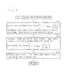
- FIG. 7 is a flow chart showing an example of the second process procedure of the luminance control method for a liquid crystal display device according to Embodiment 1 of the present invention.
- an input of a desired luminance set value (which will be hereinafter referred to as the maximum luminance L TMAX by a user of the liquid crystal display device 1 is accepted through the operation unit 5 (step S11).
- the maximum luminance L TMAX may be inputted directly as a value itself, or accepted in a manner that a table in which a luminance level is associated with the maximum luminance L TMAX as shown in FIG. 8 is stored in the storage unit 6 and the user selects a luminance level after reading the table in a suitable manner.
- the control unit 2 reads the luminances L MH , L ML and the output values AD H , AD L stored in the storage unit 6 and calculates an output value AD T which gives the maximum luminance L TMAX based on the expression (4) from the read luminances L MH , L ML and output values AD H , AD L and the maximum luminance L TMAX accepted in the step S11 (step S12).
- the luminance of the display screen of the liquid crystal panel can be controlled so as to be the maximum luminance L TMAX by controlling the backlight power supply circuit 10 so as to give the output value AD T .
- the control unit 2 then reads the normalized luminance L 0 /L 1023 , L 1 /L 1023 , ..., L 1023 /L 1023 stored in the storage unit 6 and multiplies the read luminance L 0 /L 1023 , L 1 /L 1023 , ..., L 1023 /L 1023 by the maximum luminance L TMAX accepted in the step S11 to calculate the actual luminance (which will be hereinafter referred to as a panel gray-level characteristic value) L TMAX ⁇ L 0 /L 1023 , L TMAX ⁇ L 1 /L 1023 , ..., L TMAX ⁇ L 1023 /L 1023 in a case of the maximum luminance L TMAX (step S13).
- the control unit 2 calculates luminance (which will be hereinafter referred to as an ideal gray-level characteristic value) T 0 , T 1 , ..., T 255 to be set in a case of the maximum luminance L TMAX based on a display function preliminarily stored in the storage unit 6 (step S14).
- the display function is the GSDF.
- the GSDF defines that the minimum luminance difference of a given target identifiable by a normal man is 1 JND (Just-Noticeable Difference) under a given observation conditions, and is a function obtained by plotting JNDs up to 1023-step assuming that the minimum luminance is 0.05cd/m 2 .
- the control unit 2 calculates JND TMAX and JND TMIN respectively for the maximum luminance L TMAX and minimum luminance L TMIN accepted in the step S11 based on an expression (5). It should be noted that the minimum luminance L TMIN is L TMAX ⁇ L 0 /L 1023 so that the luminance difference between each JND (each gray level) becomes the maximum, i.e. the maximum dynamic range.
- the minimum luminance L TMIN may be an arbitrary luminance of the L TMAX ⁇ L 1 /L 1023 , L TMAX ⁇ L 2 /L 1023 , ..., L TMAX ⁇ L 1023 /L 1023 , or may be obtained in a manner that input of a desired minimum luminance L TMIN by the user of the liquid crystal display device 1 is accepted through the operation unit 5.
- JND A + B ⁇ log 10 ( L ) + C ⁇ ( log 10 ( L ) ) 2 + D ⁇ ( log 10 ( L ) ) 3 + E ⁇ ( log 10 ( L ) ) 4 + F ⁇ ( log 10 ( L ) ) 5 + G ⁇ ( log 10 ( L ) ) 6 + H ⁇ ( log 10 ( L ) ) 7 + I ⁇ ( log 10 ( L ) ) 8
- D 9.8247004
- E 0.28175407
- F -1.1878455
- G -0.18014349
- H 0.14710899
- I -0.017046845
- the control unit 2 calculates an ideal gray-level characteristic value T 1 , T 2 , ..., T 255 in each gray level based on an expression (6). It should be noted that, though the above description explained an example where the display function is the GSDF, it is needless to say that the display function may be any function.
- L ( k ) 10 L ⁇ ( JND T MAX ⁇ JND T MIN 255 ) i + JND T MIN ⁇ i: gray level (0, 1, ..., 255)
- the control unit 2 compares the ideal gray-level characteristic value T 0 , T 1 , ..., T 255 calculated in the step S14 with the panel gray-level characteristic value L TMAX ⁇ L 0 /L 1023 , L TMAX ⁇ L 1 /L 1023 , ..., L TMAX ⁇ L 1023 /L 1023 calculated in the step S13 to generate the LUT 6a and stores the LUT 6a in the storage unit 6 (step S15).
- FIG. 9 is a flow chart showing an example of the LUT generating/storing process.
- the calculated gray level i is then stored in the storage unit 6 as an index of the LUT 6a and the input level j is stored in the storage unit 6 as a value of the LUT 6a (step S23).
- the LUT 6a is composed of a combination of a gray level i and an input level j which gives the minimum absolute value of the differential value (T i ⁇ L TMAX ⁇ L j /L 1023 ) in the step S22
- the present invention is not limited to this, and the LUT 6a may be composed of a combination of a gray level i and an input level j which gives the smallest positive number (or negative number) of the differential value (T i ⁇ L TMAX ⁇ L j /L 1023 ).
- Embodiment 1 is an embodiment suitable mainly for a monochrome liquid crystal display device which uses one LUT for luminance control, it is preferable to prepare an LUT for luminance control for each color in a case of a color liquid crystal display device since the transmittance of light in the liquid crystal material differs according to the wavelength of the light as shown in the expression (1).
- Such construction is described in Embodiment 2.
- FIG. 10 is a block diagram showing a structure example of a liquid crystal display device according to Embodiment 2 of the present invention.
- a liquid crystal display device 31 according to this embodiment comprises a control unit 2, a ROM 3, a RAM 4, an operation unit 5, a storage unit 36, a signal input unit 7, a liquid crystal drive circuit 8, a liquid crystal panel 9, a backlight power supply circuit 10, a backlight 11, a photosensor 12, and an ADC 13.
- the storage unit 36 which is a device rewritable as software, stores: an output value AD H of the ADC 13 and a luminance L MH of a substantially center part of the display surface of the liquid crystal panel 9 in a case of the maximum brightness (100%); an output value AD L of the ADC 13 and a luminance L ML of a substantially center part of the display surface of the liquid crystal panel 9 in a case of the minimum brightness (0%); and a first color luminance R 0 /R 1023 , R 1 /R 1023 , ..., R 1023 /R 1023 , a second color luminance G 0 /G 1023 , G 1 /G 1023 , ..., G 1023 /G 1023 , and a third color luminance B 0 /B 1023 , B 1 /B 1023 , ..., B 1023 /B 1023 which are obtained by normalizing a first color luminance R 0 , R 1 , ..., R 1023 ,
- the storage unit 36 further has a function of timely updating and storing an LUT 36a, 36b, 36c for each color in which a gray level is associated with an input level to the liquid crystal panel 9 according to the gray level.
- the content of the LUTs 36a, 36b and 36c are respectively the same as the conventional LUT illustrated in FIG. 14. Since other structures are the same as those of Embodiment 1, like codes are used to refer to like parts and the explanation thereof is omitted.
- an external photosensor 42 is a device for measuring the luminance in a wavelength band corresponding to visible light of light emitted through the liquid crystal panel 9 and the luminance in wavelength bands corresponding respectively to the three primary colors, and is additionally used when a first process procedure (mentioned later) is performed.
- the primary three colors include a color mixing system composed of red, green and blue, and a subtractive color system composed of yellow, cyan and magenta, and any one of the color systems may be employed.
- FIG. 11 is a flow chart showing an example of the first process procedure of a luminance control method for a liquid crystal display device according to Embodiment 2 of the present invention.
- the control unit 2 controls the liquid crystal drive circuit 8 to give the maximum light transmittance of the liquid crystal material (input level: 1023) (step S31).
- the control unit 2 then controls the backlight power supply circuit 10 to give the maximum brightness value (100%), obtains a luminance L MH of a substantially center part of the display surface of the liquid crystal panel 9 with the external photosensor 42 and obtains an output value AD H of the ADC 13 (step S32).
- the control unit 2 controls the backlight power supply circuit 10 to give the minimum brightness value (0%), obtains a luminance L ML of a substantially center part of the display surface of the liquid crystal panel 9 with the external photosensor 42 and obtains an output value AD L of the ADC 13 (step S33).
- the control unit 2 stores in the storage unit 36 the luminances L MH , L ML and the output values AD H , AD L obtained in the steps S32 and S33 (step S34).
- the control unit 2 then outputs a signal, which gives an input level 0, 1, ..., 1023, to the source driver 8b, outputs an output voltage V 0 , V 1 , ..., V 1023 to the liquid crystal panel 9 to change the light transmittance of the liquid crystal material, and obtains a first color luminance R 0 , R 1 , ..., R 1023 , a second color luminance G 0 , G 1 , ..., G 1023 , and a third color luminance B 0 , B 1 , ..., B 1023 of a substantially center part of the display surface of the liquid crystal panel 9 in each case with the external photosensor 42 (step S35).
- a signal which gives an input level of 0, 1, ..., 1023 may be inputted externally from a PC or the like.
- the control unit 2 then divides the first color luminance R 1023 , the second color luminance G 1023 and the third color luminance B 1023 respectively by the luminance L MH and stores in the storage unit 36 R 1023 /L MH (which will be hereinafter referred to as RR), G 1023 /L MH (which will hereinafter referred to as GR) and B 1023 /L MH (which will be hereinafter referred to as BR) (step S37). That is, a ratio of the luminance of the three primary colors RR:GR:BR is calculated.
- a ratio of the luminance is calculated in this example where the luminance liquid crystal material has the controllable maximum transmittance, a ratio of the luminance in a case where the liquid crystal material has a predetermined transmittance may be calculated.
- FIG. 12 is a flow chart showing an example of a second process procedure of the luminance control method for a liquid crystal display device according to Embodiment 2 of the present invention.
- step S41 input of a desired maximum luminance L TMAX by the user of the liquid crystal display device 1 is accepted through the operation unit 5 (step S41).
- the control unit 2 then reads the luminances L MH , L ML and output values AD H , AD L stored in the storage unit 36 and calculates an output value AD T which gives the maximum luminance L TMAX based on the expression (4) from the read luminances L MH , L ML and output values AD H , AD L and the maximum luminance L TMAX accepted in the step S41 (step S42).
- the control unit 2 then reads the normalized first color luminance R 0 /R 1023 , R 1 /R 1023 , ..., R 1023 /R 1023 , second color luminance G 0 /G 1023 , G 1 /G 1023 , ..., G 1023 /G 1023 , and third color luminance B 0 /B 1023 , B 1 /B 1023 , ..., B 1023 /B 1023 stored in the storage unit 36 and calculates panel gray-level characteristic values for the respective colors L TMAX ⁇ RR ⁇ R 0 /R 1023 , L TMAX ⁇ RR ⁇ R 1 /R 1023 , ..., L TMAX ⁇ RR ⁇ R 1023 /R 1023 , L TMAX ⁇ GR ⁇ G 0 /G 1023 , L TMAX ⁇ GR ⁇ G 1 /G 1023 , ..., L TMAX ⁇ GR ⁇ G 1023 /G 1023 , and L TMAX
- a first color raster screen may be displayed by setting a voltage to be applied to pixels of the first color as V 1023 and setting a voltage to be applied to pixels of the other colors as V 0 in order to obtain the first color luminance with the external photosensor 42.
- V 1023 a voltage to be applied to pixels of the first color
- V 0 a voltage to be applied to pixels of the other colors
- a gray-level characteristic having superior accuracy can be realized since the effect of the luminance of the second color and the third color on the luminance of the first color can be removed even when the wavelength bands of the respective colors are broad and overlap with each other (the same for the second color luminance and the third color luminance).
- the photosensor 12 converts the luminance in the wavelength band of visible light into an analog signal in the above description
- the luminance-output value characteristic for each color may be obtained using a photosensor for converting the luminance in the wavelength band of each of the three primary colors into an analog signal having a voltage according to the luminance.
- the analog signal is converted into a digital signal by connecting an ADC corresponding to each color with the photosensor. It is needless to say that a plurality of photosensors for converting the luminance of each of wavelength bands into an analog signal may be used.
- the above-mentioned process procedure may be executed for color temperatures, e.g. a blue base (12500K) and a clear base (7500K) respectively.
- the storage unit 36 stores in the first process procedure the luminances L MH , L ML and the output values AD H , AD L for each color temperature and the normalized first color luminance R 0 /R 1023 , R 1 /R 1023 , ..., R 1023 /R 1023 , second color luminance G 0 /G 1023 , G 1 /G 1023 , ..., G 1023 /G 1023 , and third color luminance B 0 /B 1023 , B 1 /B 1023 , ..., B 1023 /B 1023 , selection of a desired color temperature by the user of the liquid crystal display device 1 is accepted through the operation unit 5 in the second process procedure, and a process is executed for the selected color temperature.
- the color temperature is not limited to these two, and may be
- Embodiment 1 and Embodiment 2 are a manner that the control unit 2 in the liquid crystal display device executes the above software process to control luminance
- a PC 21 connected with the liquid crystal device via a communication line compatible with the USB standard may perform a process similar to that of the above control unit 2.
- a necessary process may be executed by reading a recording medium such as a CD-ROM or a flexible disk (FD) in which the above process content is recorded as a computer program with a CD-ROM drive or a FD drive and by loading the read computer program to a memory.
- a recording medium such as a CD-ROM or a flexible disk (FD) in which the above process content is recorded as a computer program with a CD-ROM drive or a FD drive
- the PC 21 may execute the process by downloading a computer program from a recording medium composed of a server device connected with a communication network such as a LAN via the communication network.
- the PC 21 may comprise a storage unit for storing the above LUT 6a (36a, 36b, 36c), or the PC 21 may cause a storage unit in the liquid crystal display device to store the LUT 6a (36a, 36b, 36c).
Landscapes
- Physics & Mathematics (AREA)
- Engineering & Computer Science (AREA)
- General Physics & Mathematics (AREA)
- Theoretical Computer Science (AREA)
- Computer Hardware Design (AREA)
- Crystallography & Structural Chemistry (AREA)
- Chemical & Material Sciences (AREA)
- Nonlinear Science (AREA)
- Mathematical Physics (AREA)
- Optics & Photonics (AREA)
- Control Of Indicators Other Than Cathode Ray Tubes (AREA)
- Liquid Crystal Display Device Control (AREA)
- Liquid Crystal (AREA)
Abstract
Description
- The present invention relates to: a luminance control method for a liquid crystal display device comprising a liquid crystal panel and a backlight disposed at the back of the liquid crystal panel; a liquid crystal display device to which the luminance control method is applied; and a computer program for realizing the luminance control method with a computer.
- A liquid crystal display device displays an image by controlling On/Off of each pixel in a liquid crystal panel on the basis of a video signal inputted from a personal computer (which will be hereinafter referred to as a PC) or the like and by applying to each pixel a data voltage according to the video signal with a built-in gate driver and a built-in source driver so as to control light transmittance determined by an electrooptical characteristic of a liquid crystal material.
- The electrooptical characteristic of a liquid crystal material is determined by the distance between facing substrates, i.e. a liquid crystal gap, as well as the characteristics of the liquid crystal material itself (e.g. birefringent index). More specifically, in a case of a TN (Twisted Nematic) liquid crystal, for example, the transmission intensity I is determined by a per se known expression (1) using a parameter of a product of the birefringent index Δn and the liquid crystal gap d of the TN liquid crystal, i.e. the retardation Δn·d. It should be noted that the liquid crystal gap d is generally designed to be the first local minimum point ((2·Δn·d)/λ=√3, λ: wavelength) of the expression (1).

- FIG. 13 is a graph showing an example of the electrooptical characteristic of a liquid crystal material, wherein the abscissa axis denotes the voltage applied to the liquid crystal material while the ordinate axis denotes the light transmittance of the liquid crystal material. Referring to FIG. 13, a continuous line A denotes a characteristic obtained when the liquid crystal gap d satisfies d=λ·√ 3/(2·Δn), a continuous line B denotes a characteristic obtained when the liquid crystal gap d satisfies d<λ·√3/(2·Δn) and a continuous line C denotes a characteristic obtained when the liquid crystal gap d satisfies d>λ·√3/(2·Δn), and it is understood that the light transmittance, which is an important quality, changes as the liquid crystal gap d changes, as shown by the above expression (1). Thus, the liquid crystal gap d, which is a parameter for determining the light transmittance of a liquid crystal display device, might be narrower or wider than a designed value due to a variation in manufacture, causing a problem that a desired light transmittance cannot be obtained and an intended gray-level display cannot be provided.
- Known as a solution for this problem is a liquid crystal display device comprising a memory for storing a look-up table (which will be hereinafter referred to as an LUT) in which a gray level represented by the inputted video signal is associated with an input level to a liquid crystal panel corresponding to the gray level, whereby a desired gray-level characteristic can be realized by converting a gray level into an input level on the basis of the LUT and correcting specific characteristics of the device (see, for example, Patent Document 1).
- The liquid crystal display device disclosed in the
Patent Document 1 measures a luminance in each input level with an external photosensor (luminance meter) provided at the front of the liquid crystal panel and evaluates an actual panel gray-level characteristic of the liquid crystal panel. A gray level and an input level, which are to be written into the LUT, are calculated from the measured panel gray-level characteristic and the desired ideal gray-level characteristic, and stored in the LUT. - FIG. 14 is a concept view showing an example of the content of the LUT. The LUT stores a gray level as an index associated with an input level as a value. It should be noted that shown is an example wherein the number of gray levels is 8 bits (256) and the input level is 10 bits (1024), i.e. 2 bits larger than the number of gray levels. The LUT stores a gray level "0" associated with an input level "0", a gray level "1" associated with an input level "5", a gray level "2" associated with an input level "8", ..., and a gray level "255" associated with an input level "1023". As shown in FIG. 15, the liquid crystal display device converts an inputted gray level (FIG. 15(a)) of each pixel into an input level (FIG. 15(b)) associated with the gray level on the basis of the LUT, and outputs it.
- FIG. 16 is an explanatory view showing the concept of luminance control using the LUT. Referring to FIG. 16, the continuous line denotes an actual gray-level characteristic of the liquid crystal panel and the broken line denotes an ideal gray-level characteristic to be set. The liquid crystal display device converts a gray level X represented by the inputted video signal into an input level Y to the liquid crystal panel on the basis of the LUT to obtain a luminance Q, which gives an ideal gray-level characteristic, so as to realize an ideal gray-level characteristic artificially.
[Patent Document 1]Japanese Patent Application Laid-Open No.2002-99238 - Ideal gray-level characteristics are divided into two groups: one changes relatively to the maximum luminance, and the other one does not change relatively to the maximum luminance. A specific example of the former is a gamma characteristic, and a specific example of the latter is the gray-scale display function (which will be hereinafter referred to as the GSDF) compatible with the DICOM (standard for a medical imaging device).
- FIG. 17 is a graph showing the gamma characteristic (γ=2.2), wherein the abscissa axis denotes a gray level and the ordinate axis denotes a luminance. The continuous line denotes a characteristic obtained when the luminance at 255-gray level (maximum luminance) is 600cd/m2 and the luminance at 0-gray level (minimum luminance) is 1cd/m2, and the broken line denotes a characteristic obtained when the maximum luminance is 300cd/m2 and the minimum luminance is 1cd/m2. The gamma characteristic is represented by a per se known expression (2). Each characteristic, when normalized by the maximum luminance, has a common characteristic (curve) despite a difference in the maximum luminance as shown in FIG. 18. Accordingly, conversion into a desired gray-scale characteristic can be performed without changing the LUT since the gray level for obtaining the same gray level does not change even when the luminance changes. That is, there is no need to change the LUT when the ideal gray-scale characteristic changes relatively to the maximum luminance.

i: gray level (0, 1, ..., 255)
γ: gamma value
Lmax: maximum luminance
Lmin: minimum luminance - FIG. 19 is a graph showing the GSDF compatible with the DICOM, wherein the abscissa axis denotes the gray level and the ordinate axis denotes the luminance. The continuous line denotes a characteristic obtained when the maximum luminance is 600cd/m2 and the minimum luminance is 1cd/m2, and the broken line denotes a characteristic obtained when the maximum luminance is 300cd/m2 and the minimum luminance is 1cd/m2. As shown in FIG. 20, each GSDF, when normalized by the maximum luminance, has a different characteristic (curve) according to the maximum luminance, differently from the above gamma characteristic. Since the gray level for obtaining the same gray level changes as the luminance changes, deviation from a desired gray-level characteristic arises unless the LUT is changed. For example, a gray level which gives the same normalized luminance Q (0.4cd/m2) is a gray level Y (203) when the maximum luminance is 600cd/m2, and is a gray level X (196) when the maximum luminance is 300cd/m2. The gray level thus differs (X≠Y). Accordingly, there arises a need to change the LUT when the ideal gray-level characteristic does not change relatively to the maximum luminance.
- However, there is a problem that change of the LUT needs measurement of an actual panel gray-level characteristic with an external photosensor every time, since the information to be stored in the LUT is conventionally obtained by measurement with an external photosensor in the production process of the liquid crystal display device. Though it is conceivable to preliminarily measure a panel gray-level characteristic for each possible maximum luminance and store a plurality of LUTs corresponding to the respective maximum luminance to perform correction, there is a problem that a rise in the cost is inevitable in this manner since a required capacity of a storage unit increases and there arises a need to generate and store a plurality of LUTs.
- The above problem is caused by the fact that the liquid crystal display device, which is not a selfluminous display device, needs a backlight as a light source and the luminance of the backlight generally changes as the backlight is used. Aspects of the change in the luminance of the backlight include a fact that time (aging time) is required until the luminance is stabilized and a fact that the luminance gradually decreases depending on cumulative operating time.
- Though it is said that the luminance of a conventional liquid crystal display device can be controlled, controlled is only the brightness, i.e. the ratio of luminance, so that a user cannot evaluate the luminance value during control (
e.g. brightness 50%) and has to rely on his own sensitivity. That is, the brightness can be controlled only qualitatively, and there is no liquid crystal display device capable of controlling the luminance as desired, although it is desirable to control the luminance quantitatively according to conditions such as user preference, use environment and the type of a screen image to be displayed. - The present invention has been made with the aim of solving the above problems, and it is an object thereof to provide a luminance control method for a liquid crystal display device capable of controlling a luminance of a backlight and setting the luminance quantitatively by uniquely obtaining the relation between the luminance of the backlight and a luminance of light emitted from the backlight through a liquid crystal panel and by uniquely calculating the luminance of light emitted from the backlight through the liquid crystal panel on the basis of the luminance of the backlight.
- Another object of the present invention is to provide a luminance control method for a liquid crystal display device capable of realizing a superior gray-level characteristic by obtaining an actual gray-level characteristic of a liquid crystal panel, by calculating a luminance to be set, i.e. a desired ideal gray-level characteristic, and by comparing both the gray-level characteristics to control the luminance.
- Still further object of the present invention is to provide a liquid crystal display device to which the luminance control method is applied and a computer program for realizing the luminance control method with a computer.
- A luminance control method according to the first aspect of the present invention is a luminance control method for a liquid crystal display device, which comprises a liquid crystal display panel and a backlight disposed at the back of the liquid crystal panel, for controlling an input level of a video signal to be inputted into the liquid crystal panel to control the transmittance of the liquid crystal panel and provide a gray-level display, wherein the liquid crystal display device further comprises luminance detecting means for detecting a luminance of the backlight, and the method comprises the steps of: measuring a luminance of light emitted from the backlight through the liquid crystal panel in a plurality of states where the liquid crystal panel has a predetermined transmittance and the backlight has a different luminance, and preliminarily storing the luminance measured in each state associated with the luminance detected by the luminance detecting means; setting a desired luminance set value of light emitted through the liquid crystal panel in a state where the liquid crystal panel has a predetermined transmittance; calculating a luminance to be detected by the luminance detecting means, which is to be the set luminance set value, on the basis of stored luminance in each state; and controlling the luminance of the backlight so as to be the calculated luminance.
- A luminance control method according to the second aspect of the present invention, as set forth in the first aspect, further comprises the steps of: measuring a luminance of light emitted through the liquid crystal panel in each input level, and preliminarily storing the measured luminance associated with an input level which gives the luminance; calculating a luminance of light emitted through the liquid crystal panel in each input level and a luminance to be set in each gray level in a case of the luminance set value on the basis of the stored luminance and input level; extracting an input level which gives a luminance substantially equal to the luminance to be set in each gray level on the basis of the luminance in each calculated input level and the luminance to be set in each gray level, and storing the extracted input level associated with a gray level; and controlling the transmittance of the liquid crystal panel in a gray level associated with the input level of the video signal.
- A luminance control method according to the third aspect of the present invention, as set forth in the first aspect, further comprises the steps of: measuring a luminance of light emitted through the liquid crystal panel in each input level; normalizing each measured luminance, and preliminarily storing each normalized luminance associated with an input level which gives the luminance; calculating a luminance of light emitted through the liquid crystal panel in each input level and a luminance to be set in each gray level in a case of the luminance set value on the basis of the stored luminance and input level; extracting an input level which gives a luminance substantially equal to the luminance to be set in each gray level on the basis of the luminance in each calculated input level and the luminance to be set in each gray level, and storing the extracted input level associated with a gray level; and controlling the transmittance of the liquid crystal panel in a gray level associated with the input level of the video signal.
- In a luminance control method according to the fourth aspect of the present invention, as set forth in any one of the first to the third aspects, the luminance set value is a luminance in a state where the transmittance of the liquid crystal panel is a controllable maximum transmittance.
- In a luminance control method according to the fifth aspect of the present invention, as set forth in any one of the first to the fourth aspects, one state of the plurality of states is a state where the backlight has a controllable maximum luminance and another state of the plurality of states is a state where the backlight has a controllable minimum luminance.
- A liquid crystal display device according to the sixth aspect of the present invention is a liquid crystal display device, which comprises a liquid crystal panel and a backlight disposed at the back of the liquid crystal panel, for controlling an input level of a video signal to be inputted to the liquid crystal panel to control the transmittance of the liquid crystal panel and provide a gray-level display, further comprising: luminance detecting means for detecting a luminance of the backlight; a storage unit for preliminarily storing information in which the luminance detected by the luminance detecting means in a plurality of states where the liquid crystal panel has a predetermined transmittance and the backlight has a different luminance is associated with a luminance of light emitted from the backlight through the liquid crystal panel; accepting means for accepting a desired luminance set value of light emitted through the liquid crystal panel in a state where the liquid crystal panel has a predetermined transmittance; calculating means for calculating a luminance to be detected by the luminance detecting means, which is to be the luminance set value accepted by the accepting means, on the basis of the information stored in the storage unit; and luminance control means for controlling the luminance of the backlight so as to be the luminance calculated by the calculating means.
- In a liquid crystal display device according to the seventh aspect of the present invention, as set forth in the sixth aspect, the storage unit further stores second information on a luminance of light emitted through the liquid crystal panel in each input level, and the device further comprises: second calculating means for calculating a luminance of light emitted through the liquid crystal panel in each input level in a case of the luminance set value accepted by the accepting means on the basis of the second information; third calculating means for calculating a luminance to be set in each gray level in a case of the luminance set value accepted by the accepting means; fourth calculating means for calculating a luminance difference between the luminance to be set in each gray level calculated by the third calculating means and the luminance in each input level calculated by the second calculating means; storage means for storing an input level, which gives a minimum luminance difference calculated by the fourth calculating means, associated with a gray level; and control means for controlling the transmittance of the liquid crystal panel in a gray level associated with the input level of the video signal.
- In a liquid crystal display device according to the eighth aspect of the present invention, as set forth in the sixth or the seventh aspect, the luminance detecting means has: photoelectric conversion means for converting the luminance of the backlight into an analog-type electric signal having a voltage corresponding to the luminance of the backlight; and analog-digital conversion means for converting the converted analog-type electric signal into a digital-type electric signal.
- A computer program according to the ninth aspect of the present invention is a computer program for causing a computer to output control information to a liquid crystal display device comprising a liquid crystal panel and a backlight disposed at the back of the liquid crystal panel and causing the computer to control an input level of a video signal to be inputted into the liquid crystal panel to control the transmittance of the liquid crystal panel and provide a gray-level display, comprising the steps of: causing the computer to store in a storage unit a luminance of the backlight, in a plurality of states where the backlight has a different luminance, associated with a luminance of light emitted from the backlight through the liquid crystal panel; causing the computer to set a desired luminance set value of light emitted through the liquid crystal panel; causing the computer to calculate control information for controlling a luminance of the backlight, which is to be the set luminance set value, on the basis of information stored in the storage unit; and causing the computer to output the calculated control information to the liquid crystal display device.
- A computer program according to the tenth aspect of the present invention, as set forth in the ninth aspect, further comprises the steps of: causing the computer to store in a storage unit second information on a luminance of light emitted through the liquid crystal panel in each input level; causing the computer to calculate a luminance of light emitted through the liquid crystal panel in each input level in a case of the inputted luminance set value on the basis of the stored second information; causing the computer to calculate a luminance to be set in each gray level in a case of the inputted luminance set value; causing the computer to calculate a luminance difference between the calculated luminance to be set in each gray level and the calculated luminance in each input level; and causing the computer to store in the storage unit an input level, which gives a minimum calculated luminance difference, associated with a gray level.
- With the first aspect, the sixth aspect and the ninth aspect, the luminance detected by the luminance detecting means and the luminance of light emitted from the backlight through the liquid crystal panel are measured in each of a plurality of states where the liquid crystal panel has a predetermined transmittance and the backlight has a different luminance, and both the luminances in each state are stored associated with each other. Since the relation between the luminance of the backlight and the luminance of light emitted from the backlight through the liquid crystal panel can be obtained uniquely, the luminance of light emitted from the backlight through the liquid crystal panel can be calculated based on the luminance of the backlight detected by the luminance detecting means. A desired luminance set value of light emitted through the liquid crystal panel is then set and the luminance of the backlight to be detected by the luminance detecting means in a case of the set luminance set value is calculated to control the luminance of the backlight. Accordingly, the luminance can be controlled so as to be a desired luminance set value, differently from conventional brightness control by which the luminance can be controlled only qualitatively. Moreover, when the luminance detected by the luminance detecting means and the luminance of light emitted from the backlight through the liquid crystal panel in a plurality of states where the backlight has a different luminance are measured in the production process of the liquid crystal display device and both the luminances in each state are preliminary stored associated with each other, there is no need to measure the luminance of light emitted through the liquid crystal panel using an external photosensor after shipment, the burden imposed on the user of the liquid crystal display device is decreased, highly accurate measurement is enabled as a series of processes, and it becomes possible to control the luminance so as to be a desired luminance with a high degree of accuracy. Furthermore, since quantitative luminance setting is enabled, the invention can be utilized as a self-diagnosis function such as notification to the user of the present luminance or notification to the user of a fact that the luminance falls below a predetermined luminance, when it occurs.
- With the second aspect, the seventh aspect and the tenth aspect, the luminance of light emitted through the liquid crystal panel in each input level is measured and the measured luminance is stored associated with an input level which gives the luminance. In this manner, an actual gray-level characteristic of the liquid crystal panel can be obtained. The luminance of light emitted through the liquid crystal panel in each input level in a case where the luminance of light emitted through the liquid crystal panel is a luminance set value and the luminance (ideal luminance) to be set in each gray level is then calculated and an input level which gives a luminance substantially equal to the ideal luminance in each gray level is extracted. Since the input level can be set so as to give a luminance substantially equal to the ideal luminance in each gray level, it becomes possible to realize a superior gray-level characteristic.
- With the third aspect, the seventh aspect and the tenth aspect, the luminance of light emitted through the liquid crystal panel in each input level is measured, each luminance of each measured input level is divided and normalized by the maximum luminance of the measured luminances, and each normalized luminance is stored associated with an input level which gives the luminance. In this manner, it is possible to obtain an actual gray-level characteristic of the liquid crystal panel. The luminance of light emitted through the liquid crystal panel in each input level in a case where the luminance of light emitted through the liquid crystal panel is the luminance set value and a luminance (ideal luminance) to be set in each gray level is then calculated and an input level which gives a luminance substantially equal to the ideal luminance in each gray level is extracted. Since the input level can be set so as to give a luminance substantially equal to the ideal luminance in each gray level, it is possible to realize a superior gray-level characteristic.
- Moreover, regarding the above measurement of the luminance of light emitted through the liquid crystal panel, when the luminance in a predetermined wavelength band and the luminance in a plurality of wavelength bands in the predetermined wavelength band are measured, the input level for each wavelength band can be set individually so as to give a luminance substantially equal to the ideal luminance in each gray level. Since luminance control can be performed individually even when each wavelength band has a different gray-level characteristic, a superior gray-level characteristic can be realized. For example, by measuring the luminance of a wavelength band corresponding to visible light as the predetermined wavelength band and measuring the luminances of wavelength bands corresponding to the three primary colors as a plurality of wavelength bands, input level can be set individually for the three primary colors so as to give a luminance substantially equal to the ideal luminance in each gray level. Though the wavelength distribution of light emitted from the backlight might change generally due to aged deterioration, a gray-level characteristic having superior color reproducibility and superior white balance can be realized since luminance control can be performed individually for the three primary colors.
- With the fourth aspect, by making a luminance in a state where the transmittance of the liquid crystal panel is a controllable maximum transmittance a luminance set value, the maximum luminance of light emitted through the liquid crystal panel can be set quantitatively.
- With the fifth aspect, by increasing the luminance difference between a plurality of states of different luminance of the backlight, the relation between the luminance of the backlight and the luminance of light emitted from the backlight through the liquid crystal panel can be obtained with a high degree of accuracy.
- With the eighth aspect, conversion of the luminance of the backlight into an analog-type electric signal having a voltage corresponding to the luminance of the backlight is performed by the photoelectric conversion means and the converted analog-type electric signal is converted into a digital-type electric signal by the analog-digital conversion means. Accordingly, the luminance detecting means can be constructed at low cost using general-purpose photoelectric conversion means and analog-digital conversion means.
- With the present invention, since the relation between the luminance of the backlight and the luminance of light emitted from the backlight through the liquid crystal panel can be obtained uniquely and the luminance of light emitted from the backlight through the liquid crystal panel can be uniquely calculated based on the luminance of the backlight, the luminance of the backlight can be controlled and the luminance can be set quantitatively.
- Moreover, with the present invention, since an actual gray-level characteristic of the liquid crystal panel can be obtained, a gray-level characteristic to be set can be calculated and both the gray-level characteristics are compared to control the luminance, and a superior gray-level characteristic can be realized.
- Furthermore, with the present invention, when the luminance of the backlight (luminance detected by the luminance detecting means) and the luminance of light emitted from the backlight through the liquid crystal panel are measured in the production process of the liquid crystal display device, since there is no need to measure the luminance of light emitted through the liquid crystal panel using an external photosensor after shipment, the burden imposed on the user of the liquid crystal display device is decreased, highly accurate measurement is enabled as a series of processes, and it becomes possible to control the luminance so as to be a desired luminance with a high degree of accuracy. Moreover, even when the gray-level characteristic does not change relatively to a change in the maximum luminance, a desired gray-level characteristic can be realized with a high degree of accuracy without using an external photosensor.
-
- FIG. 1 is a block diagram showing a structure example of a liquid crystal display device according to
Embodiment 1 of the present invention; - FIG. 2 is a diagram showing an input-output characteristic of a source driver;
- FIG. 3 is a flow chart showing an example of a first process procedure of a luminance control method for a liquid crystal display device according to
Embodiment 1 of the present invention; - FIG. 4 is a graph showing a luminance-output value characteristic;
- FIG. 5 is a graph showing an actual gray-level characteristic of the liquid crystal panel;
- FIG. 6 is a graph showing a normalized gray-scale characteristic of the liquid crystal panel;
- FIG. 7 is a flow chart showing an example of a second process procedure of a luminance control method for a liquid crystal display device according to
Embodiment 1 of the present invention; - FIG. 8 is a table view composed of a luminance level and the maximum luminance LTMAX;
- FIG. 9 is a flow chart showing an example of an LUT generating/storing process;
- FIG. 10 is a block diagram showing a structure example of a liquid crystal display device according to
Embodiment 2 of the present invention; - FIG. 11 is a flow chart showing an example of a first process procedure of a luminance control method for a liquid crystal display device according to
Embodiment 2 of the present invention; and - FIG. 12 is a flow chart showing an example of a second process procedure of a luminance control method for a liquid crystal display device according to
Embodiment 2 of the present invention. - FIG. 13 is a graph showing an example of the electrooptical characteristic of a liquid crystal material;
- FIG. 14 is a concept view showing an example of the content of an LUT;
- FIG. 15 is an explanatory view showing each pixel level before and after luminance control using the LUT;
- FIG. 16 is an explanatory view showing the concept of luminance control using the LUT;
- FIG. 17 is a graph showing a gamma characteristic;
- FIG. 18 is a graph of a normalized gamma characteristic;
- FIG. 19 is a graph showing the GSDF compatible with the DICOM;
- FIG. 20 is a graph of a normalized GSDF;
-
- 1, 31
- Liquid crystal display device
- 2
- Control unit
- 3
- ROM
- 4
- RAM
- 5
- Operation unit
- 6, 36
- Storage unit
- 6a, 36a, 36b, 36c
- LUT
- 7
- Signal input unit
- 8
- Liquid crystal drive circuit
- 9
- Liquid crystal panel
- 10
- Backlight power supply circuit
- 11
- Backlight
- 12
- Photosensor
- 13
- ADC
- 22, 42
- External photosensor
- The following description will explain the present invention in detail with reference to the drawings illustrating some embodiments thereof.
- FIG. 1 is a block diagram showing a structure example of a liquid crystal display device according to
Embodiment 1 of the present invention. The liquidcrystal display device 1 according to this embodiment comprises acontrol unit 2, aROM 3, aRAM 4, anoperation unit 5, astorage unit 6, asignal input unit 7, a liquidcrystal drive circuit 8, aliquid crystal panel 9, a backlightpower supply circuit 10, abacklight 11, aphotosensor 12, and an ADC (A/D converter) 13. The liquidcrystal display device 1 has a function of displaying a screen image on a display screen of theliquid crystal panel 9 on the basis of a video signal inputted through thesignal input unit 7. Though the video signal might be of an analog type, the following description will explain a digital-type video signal. It should be noted that anexternal photosensor 22 is a device for measuring the luminance of light emitted through theliquid crystal panel 9, and is additionally used when the following first process procedure is performed. - The
control unit 2, which is specifically composed of a CPU connected with each hardware unit mentioned above through abus 15, controls each hardware unit and performs a variety of software functions according to a control program stored in theROM 3. TheROM 3 preliminarily stores a variety of software programs necessary for operations of the liquid crystal device as mentioned above. TheRAM 4, which is composed of a SRAM, stores temporal data which is generated when the software is executed. It should be noted that thecontrol unit 2, theROM 3, theRAM 4 and the like may be realized by anelectronic circuit 16 such as a microcomputer so as to a execute a variety of processes as hardware. - The
operation unit 5 comprises various function keys for operating the liquidcrystal display device 1. The function keys include a luminance control execution key 5a for setting whether a luminance control process is to be performed or not and a luminance setting key 5b for setting the luminance of the liquid crystal display device. It should be noted that an On Screen Display (OSD) may be displayed on theliquid crystal panel 9 so as to operate various settings of the liquid crystal display device, or theliquid crystal panel 9 may be of a touch panel type so that a part of, or all of, various function keys of theoperation unit 5 can be substituted. - The
storage unit 6, which is a device rewritable as software, stores: an output value ADH of theADC 13 and a luminance LMH of a substantially center part of the display surface of theliquid crystal panel 9 obtained when the brightness is the maximum (100%); an output value ADL of theADC 13 and a luminance LML of a substantially center part of the display surface of the liquid crystal panel obtained when the brightness is the minimum (0%); and luminance L0/L1023, L1/L1023, ..., L1023/L1023 which is obtained by normalizing the luminance L0, L1, ..., L1023 of a substantially center part of the display surface obtained when a source driver (mentioned later) outputs an output voltage for each input level (e.g. 10 bit: 0~1023) to the liquid crystal panel. Thestorage unit 6 further has a function of timely updating and storing an LUT 6a in which a gray level is associated with an input level to the liquid crystal panel corresponding to the gray level. The content of the LUT 6a is the same as the conventional LUT illustrated in FIG. 14. - The
signal input unit 7, which is connected to anexternal PC 21 through a video signal line L, receives a video signal outputted from thePC 21, and thecontrol unit 2 corrects the received video signal on the basis of the LUT 6a stored in thestorage unit 6 and outputs it to the liquidcrystal drive circuit 8. The liquidcrystal drive circuit 8, which is composed chiefly of a gate driver 8a and asource driver 8b, drives theliquid crystal panel 9 on the basis of a video signal (corrected signal) inputted from thecontrol unit 2. In this manner, thecontrol unit 2 can control the transmittance of theliquid crystal panel 9 in a gray level associated with an input level of the video signal outputted from thePC 21. - Supplied to the
source driver 8b, which has an input-output characteristic shown in FIG. 2, is a reference voltage (when 10 bit: VREF1, VREF2, ..., VREF10), and thesource driver 8b has a function of generating an output voltage according to an input level inputted from thecontrol unit 2 and outputting it in each output stage. That is, thesource driver 8b outputs the output voltage (data voltage) V0, V1, ..., V1023 to a source line of the liquid crystal panel according to the inputtedinput level - The
liquid crystal panel 9 is constructed by disposing a pair of glass substrates opposite to each other and forming a liquid crystal layer made of liquid crystal materials in a gap between them. A plurality of pixel electrodes and a TFT whose drain is connected to the respective pixel electrodes are formed on one glass substrate and a common electrode is formed on the other glass substrate. The gate and the source of the TFT are connected sequentially with each output stage of the gate driver 8a and thesource driver 8b, respectively. Theliquid crystal panel 9 is fitted between a pair of polarizing plates, and thebacklight 11 is disposed at the back thereof. - The backlight
power supply circuit 10 has a function of controlling an output voltage thereof and functions as luminance control means for controlling the luminance of light emitted from thebacklight 11 by outputting a controlled voltage to thebacklight 11. Theliquid crystal panel 9 controls the light transmittance determined by an electrooptical characteristic of a liquid crystal material and displays a screen image by controlling On/Off of each pixel by a gate signal inputted from the gate driver 8a and by applying an output voltage (data voltage) inputted from thesource driver 8b to each pixel during the On period. - Disposed near the
backlight 11 is ageneral purpose photosensor 12, such as a photodiode or a phototransistor, which converts incident light from thebacklight 11 into an analog-type electric signal (which will be hereinafter referred to as an analog signal) having a voltage according to the luminance (e.g. the luminance in the wavelength band of the visible light) of the incident light. TheADC 13 converts the analog signal outputted from the photosensor 12 into a digital-type electric signal (which will be hereinafter referred to as a digital signal). That is, thephotosensor 12 and theADC 13 cooperate to function as luminance detecting means according to the present invention. - Now, the following description will explain a luminance control method for a liquid crystal display device according to the present invention, using a flow chart. The luminance control method for a liquid crystal display device according to the present invention includes a first process procedure, which uses an
external photosensor 22, and a second process procedure, which does not use theexternal photosensor 22. It should be noted that the first process procedure is generally processed by a manufacturer of the liquid crystal device, i.e. processed in manufacturing process, and the second process procedure is processed by the user of the liquid crystal display device. - FIG. 3 is a flow chart showing an example of the first process procedure of the luminance control method for a liquid crystal display device according to
Embodiment 1 of the present invention. - First, the
control unit 2 controls the liquidcrystal drive circuit 8 to give the maximum light transmittance of the liquid crystal material (step S1). In particular, when theliquid crystal panel 9 is in a normally black mode, thecontrol unit 2 outputs a scanning signal to the gate driver 8a and outputs to thesource driver 8b an input level (e.g. "1111111111(1023)" in a case of 10-bit input) which gives the maximum voltage to be applied to the liquid crystal material. The gate driver 8a outputs a scanning voltage for controlling On/Off of the TFT sequentially to each output stage in synchronization with the scanning signal inputted from thecontrol unit 2 so as to supply the scanning voltage to the gate line of the liquid crystal panel. Thesource driver 8b outputs an output voltage (data voltage) V1023 corresponding to the inputted input level (1023) to each output stage and to the source line of the liquid crystal panel. In this manner, each TFT applies the data voltage V1023 to a pixel electrode and controls the light transmittance of the liquid crystal material determined by the electrooptical characteristic. It should be noted that, when theliquid crystal panel 9 is in a normally white mode, the light transmittance of the liquid crystal material can be maximum by outputting to thesource driver 8b an input level (e.g. "0000000000(0)" in a case of 10-bit input) which gives the minimum voltage to be applied to the liquid crystal material. A signal of an input level which gives the maximum light transmittance of the liquid crystal material may be inputted externally from a PC or the like. - The
control unit 2 then controls the backlightpower supply circuit 10 to give the maximum brightness value (100%), obtains a luminance LMH of a substantially center part of the display surface of theliquid crystal panel 9 with theexternal photosensor 22 and obtains an output value ADH of the ADC 13 (step S2). Similarly, thecontrol unit 2 controls the backlightpower supply circuit 10 to give the minimum brightness value (0%), obtains a luminance LML of a substantially center part of the display surface of theliquid crystal panel 9 and obtains an output value ADL of the ADC 13 (step S3). It should be noted that the brightness control can be performed by controlling the voltage value to be supplied to the backlight. - The
control unit 2 stores in thestorage unit 6 the luminances LMH, LML and the output values ADH, ADL obtained in the steps S2 and S3 (step S4). Since the luminance L is proportional to the output value AD, a luminance-output value characteristic as shown in FIG. 4 can be obtained uniquely by obtaining two points of brightness, namely 100% and 0%, and the luminance L can be calculated (interpolated) based on an expression (3) from the output value AD of theADC 13, the luminances LMH, LML and the output values ADH, ADL, without using theexternal photosensor 22. That is, the output value AD of theADC 13, which gives the luminance L, can be calculated based on an expression (4). It should be noted that, though two points of 100% and 0% of the brightness are obtained in this example to determine the luminance-output value characteristic, the present invention is not limited to this, and the luminances and the output values of two arbitrary points of the different brightness may be obtained and the obtained luminances and output values may be stored in thestorage unit 6 to obtain the luminance-output value characteristic by forward extrapolation or backward extrapolation, or the luminances and the output values of more than two arbitrary points of the different brightness may be obtained and linearization may be applied to obtain the luminance-output value characteristic.

- The
control unit 2 then outputs to thesource driver 8b a signal, which gives the input level of 0, 1, ..., 1023, to output the output voltage V0, V1, ..., V1023 to theliquid crystal panel 9 and change the light transmittance of the liquid crystal material, and obtains the luminance L0, L1, ..., L1023 of a substantially center part of theliquid crystal panel 9 in each case with the external photosensor 22 (step S5). In this manner, an actual gray-level characteristic of theliquid crystal panel 9 as shown in FIG. 5 can be obtained. A signal which gives the input level of 0, 1, ..., 1023 may be inputted externally from a PC or the like. - The obtained luminance L0, L1, ..., L1023 is then normalized by dividing it by the maximum luminance L1023 and the normalized luminance L0/L1023, L1/L1023, ..., L1023/L1023 is stored in the storage unit 6 (step S6). In this manner, a normalized gray-level characteristic of the
liquid crystal panel 9 as shown in FIG. 8 can be obtained. It is needless to say that an actual gray-level characteristic obtained in the step S5 may be stored in thestorage unit 6 instead of the normalized gray-level characteristic, and there is no limitation as long as a correlation between luminances for respective input levels inputted to the source driver is defined. Furthermore, 256 points of the luminance to give input levels of 0, 4, 8, ..., 1023, for example, of the input levels of 0, 1, ..., 1023 may be measured, and the luminance of 1024 points may be calculated by linear interpolation, normalized and then stored in thestorage unit 6. In this manner, reduction of process time can be realized. It is needless to say that the 256 points of input levels to be measured actually may be arbitrary, and the number of the levels to be measured actually is not limited to 256. - FIG. 7 is a flow chart showing an example of the second process procedure of the luminance control method for a liquid crystal display device according to
Embodiment 1 of the present invention. - First, an input of a desired luminance set value (which will be hereinafter referred to as the maximum luminance LTMAX by a user of the liquid
crystal display device 1 is accepted through the operation unit 5 (step S11). It should be noted that the maximum luminance LTMAX may be inputted directly as a value itself, or accepted in a manner that a table in which a luminance level is associated with the maximum luminance LTMAX as shown in FIG. 8 is stored in thestorage unit 6 and the user selects a luminance level after reading the table in a suitable manner. - The
control unit 2 reads the luminances LMH, LML and the output values ADH, ADL stored in thestorage unit 6 and calculates an output value ADT which gives the maximum luminance LTMAX based on the expression (4) from the read luminances LMH, LML and output values ADH, ADL and the maximum luminance LTMAX accepted in the step S11 (step S12). In this manner, the luminance of the display screen of the liquid crystal panel can be controlled so as to be the maximum luminance LTMAX by controlling the backlightpower supply circuit 10 so as to give the output value ADT. - The
control unit 2 then reads the normalized luminance L0/L1023, L1/L1023, ..., L1023/L1023 stored in thestorage unit 6 and multiplies the read luminance L0/L1023, L1/L1023, ..., L1023/L1023 by the maximum luminance LTMAX accepted in the step S11 to calculate the actual luminance (which will be hereinafter referred to as a panel gray-level characteristic value) LTMAX·L0/L1023, LTMAX·L1/L1023, ..., LTMAX·L1023/L1023 in a case of the maximum luminance LTMAX (step S13). - The
control unit 2 then calculates luminance (which will be hereinafter referred to as an ideal gray-level characteristic value) T0, T1, ..., T255 to be set in a case of the maximum luminance LTMAX based on a display function preliminarily stored in the storage unit 6 (step S14). Now, the following description will explain an example where the display function is the GSDF. The GSDF defines that the minimum luminance difference of a given target identifiable by a normal man is 1 JND (Just-Noticeable Difference) under a given observation conditions, and is a function obtained by plotting JNDs up to 1023-step assuming that the minimum luminance is 0.05cd/m2. - The
control unit 2 calculates JNDTMAX and JNDTMIN respectively for the maximum luminance LTMAX and minimum luminance LTMIN accepted in the step S11 based on an expression (5). It should be noted that the minimum luminance LTMIN is LTMAX·L0/L1023 so that the luminance difference between each JND (each gray level) becomes the maximum, i.e. the maximum dynamic range. It is needless to say that the minimum luminance LTMIN may be an arbitrary luminance of the LTMAX·L1/L1023, LTMAX·L2/L1023, ..., LTMAX·L1023/L1023, or may be obtained in a manner that input of a desired minimum luminance LTMIN by the user of the liquidcrystal display device 1 is accepted through theoperation unit 5.
A=71.498068, B=94.593053, C=41.912053
D=9.8247004, E=0.28175407, F=-1.1878455
G=-0.18014349, H=0.14710899, I=-0.017046845 - In order to allocate a resolution n (e.g. 8 bit=256) a JND difference (JNDTMAX-JNDTMIN) between the maximum luminance LTMAX and the minimum luminance LTMIN, which is divided equally into the number of the gray levels 2n-1 (255 in this example), the
control unit 2 calculates an ideal gray-level characteristic value T1, T2, ..., T255 in each gray level based on an expression (6). It should be noted that, though the above description explained an example where the display function is the GSDF, it is needless to say that the display function may be any function.
i: gray level (0, 1, ..., 255)
a=-1.3011877, b=-2.5840191E-2, c=8.0242636E-2
d=-1.0320229E-1, e=1.3646699E-1, f=2.8745620E-2
g=-2.5468404E-2, h=-3.1978977E-3
p=1.2992634E-4, q=1.3635334E-3 - The
control unit 2 then compares the ideal gray-level characteristic value T0, T1, ..., T255 calculated in the step S14 with the panel gray-level characteristic value LTMAX·L0/L1023, LTMAX·L1/L1023, ..., LTMAX·L1023/L1023 calculated in the step S13 to generate the LUT 6a and stores the LUT 6a in the storage unit 6 (step S15). - Now, the following description will explain the LUT generating/storing process mentioned above in the step S15 more concretely. FIG. 9 is a flow chart showing an example of the LUT generating/storing process.
- The
control unit 2 calculates a differential value (Ti-LTMAX·Lj/L1023) between an ideal gray-level characteristic value Ti (i=0, 1, ..., 255) and a panel gray-level characteristic value LTMAX·Lj/L1023 (j=0, 1, ..., 1023) (step S21), and extracts a combination of a gray level i and an input level j, which gives the minimum absolute value of the calculated differential value |Ti-LTMAX·Lj/L1023|, for each gray level i (step S22). - The calculated gray level i is then stored in the
storage unit 6 as an index of the LUT 6a and the input level j is stored in thestorage unit 6 as a value of the LUT 6a (step S23). It should be noted that, though described is a manner in that the LUT 6a is composed of a combination of a gray level i and an input level j which gives the minimum absolute value of the differential value (Ti―LTMAX·Lj/L1023) in the step S22, the present invention is not limited to this, and the LUT 6a may be composed of a combination of a gray level i and an input level j which gives the smallest positive number (or negative number) of the differential value (Ti―LTMAX·Lj/L1023). - Though described in
Embodiment 1 is an embodiment suitable mainly for a monochrome liquid crystal display device which uses one LUT for luminance control, it is preferable to prepare an LUT for luminance control for each color in a case of a color liquid crystal display device since the transmittance of light in the liquid crystal material differs according to the wavelength of the light as shown in the expression (1). Such construction is described inEmbodiment 2. - FIG. 10 is a block diagram showing a structure example of a liquid crystal display device according to
Embodiment 2 of the present invention. A liquidcrystal display device 31 according to this embodiment comprises acontrol unit 2, aROM 3, aRAM 4, anoperation unit 5, astorage unit 36, asignal input unit 7, a liquidcrystal drive circuit 8, aliquid crystal panel 9, a backlightpower supply circuit 10, abacklight 11, aphotosensor 12, and anADC 13. - The
storage unit 36, which is a device rewritable as software, stores: an output value ADH of theADC 13 and a luminance LMH of a substantially center part of the display surface of theliquid crystal panel 9 in a case of the maximum brightness (100%); an output value ADL of theADC 13 and a luminance LML of a substantially center part of the display surface of theliquid crystal panel 9 in a case of the minimum brightness (0%); and a first color luminance R0/R1023, R1/R1023, ..., R1023/R1023, a second color luminance G0/G1023, G1/G1023, ..., G1023/G1023, and a third color luminance B0/B1023, B1/B1023, ..., B1023/B1023 which are obtained by normalizing a first color luminance R0, R1, ..., R1023, a second color luminance G0, G1, ..., G1023, and a third color luminance B0, B1, ..., B1023 corresponding to the three primary colors of a substantially center part of the display surface obtained when thesource driver 8b outputs an output voltage corresponding to each input level to theliquid crystal panel 9. Thestorage unit 36 further has a function of timely updating and storing an LUT 36a, 36b, 36c for each color in which a gray level is associated with an input level to theliquid crystal panel 9 according to the gray level. The content of the LUTs 36a, 36b and 36c are respectively the same as the conventional LUT illustrated in FIG. 14. Since other structures are the same as those ofEmbodiment 1, like codes are used to refer to like parts and the explanation thereof is omitted. - It should be noted that an external photosensor 42 is a device for measuring the luminance in a wavelength band corresponding to visible light of light emitted through the
liquid crystal panel 9 and the luminance in wavelength bands corresponding respectively to the three primary colors, and is additionally used when a first process procedure (mentioned later) is performed. It should be also noted that the primary three colors include a color mixing system composed of red, green and blue, and a subtractive color system composed of yellow, cyan and magenta, and any one of the color systems may be employed. - FIG. 11 is a flow chart showing an example of the first process procedure of a luminance control method for a liquid crystal display device according to
Embodiment 2 of the present invention. - First, the
control unit 2 controls the liquidcrystal drive circuit 8 to give the maximum light transmittance of the liquid crystal material (input level: 1023) (step S31). Thecontrol unit 2 then controls the backlightpower supply circuit 10 to give the maximum brightness value (100%), obtains a luminance LMH of a substantially center part of the display surface of theliquid crystal panel 9 with the external photosensor 42 and obtains an output value ADH of the ADC 13 (step S32). Similarly, thecontrol unit 2 controls the backlightpower supply circuit 10 to give the minimum brightness value (0%), obtains a luminance LML of a substantially center part of the display surface of theliquid crystal panel 9 with the external photosensor 42 and obtains an output value ADL of the ADC 13 (step S33). Thecontrol unit 2 stores in thestorage unit 36 the luminances LMH, LML and the output values ADH, ADL obtained in the steps S32 and S33 (step S34). - The
control unit 2 then outputs a signal, which gives aninput level source driver 8b, outputs an output voltage V0, V1, ..., V1023 to theliquid crystal panel 9 to change the light transmittance of the liquid crystal material, and obtains a first color luminance R0, R1, ..., R1023, a second color luminance G0, G1, ..., G1023, and a third color luminance B0, B1, ..., B1023 of a substantially center part of the display surface of theliquid crystal panel 9 in each case with the external photosensor 42 (step S35). The obtained first color luminance R0, R1, ..., R1023, second color luminance G0, G1, ..., G1023, and third color luminance B0, B1, ..., B1023 are then normalized by dividing them respectively by the maximum luminance R1023, G1023 and B1023, and the normalized first color luminance R0/R1023, R1/R1023, ..., R1023/R1023, second color luminance G0/G1023, G1/G1023, ..., G1023/G1023, and third color luminance B0/B1023, B1/B1023, ..., B1023/B1023 are stored in the storage unit 36 (step S36). A signal which gives an input level of 0, 1, ..., 1023 may be inputted externally from a PC or the like. - The
control unit 2 then divides the first color luminance R1023, the second color luminance G1023 and the third color luminance B1023 respectively by the luminance LMH and stores in the storage unit 36 R1023/LMH (which will be hereinafter referred to as RR), G1023/LMH (which will hereinafter referred to as GR) and B1023/LMH (which will be hereinafter referred to as BR) (step S37). That is, a ratio of the luminance of the three primary colors RR:GR:BR is calculated. It should be noted that, though a ratio of the luminance is calculated in this example where the luminance liquid crystal material has the controllable maximum transmittance, a ratio of the luminance in a case where the liquid crystal material has a predetermined transmittance may be calculated. - FIG. 12 is a flow chart showing an example of a second process procedure of the luminance control method for a liquid crystal display device according to
Embodiment 2 of the present invention. - First, input of a desired maximum luminance LTMAX by the user of the liquid
crystal display device 1 is accepted through the operation unit 5 (step S41). Thecontrol unit 2 then reads the luminances LMH, LML and output values ADH, ADL stored in thestorage unit 36 and calculates an output value ADT which gives the maximum luminance LTMAX based on the expression (4) from the read luminances LMH, LML and output values ADH, ADL and the maximum luminance LTMAX accepted in the step S41 (step S42). - The
control unit 2 then reads the normalized first color luminance R0/R1023, R1/R1023, ..., R1023/R1023, second color luminance G0/G1023, G1/G1023, ..., G1023/G1023, and third color luminance B0/B1023, B1/B1023, ..., B1023/B1023 stored in thestorage unit 36 and calculates panel gray-level characteristic values for the respective colors LTMAX·RR·R0/R1023, LTMAX·RR·R1/R1023, ..., LTMAX·RR·R1023/R1023, LTMAX·GR·G0/G1023, LTMAX·GR·G1/G1023, ..., LTMAX·GR·G1023/G1023, and LTMAX·BR·B0/B1023, LTMAX·BR·B1/B1023, ..., LTMAX·BR·B1023/B1023 in a case of the maximum luminance LTMAX by multiplying the read first color luminance R0/R1023, R1/R1023, ..., R1023/R1023, second color luminance G0/G1023, G1/G1023, ..., G1023/G1023, and third color luminance B0/B1023, B1/B1023, ..., B1023/B1023 by RR, GR and BR normalized in the step S37 and the maximum value LTMAX accepted in the step S41 (step S43). - The
control unit 2 then calculates ideal gray-level characteristic values for the respective colors TR0, TR1, ..., TR255, TG0, TG1, ..., TG255, and TB0, TB1, ..., TB255 in a case of the maximum luminance LTMAX based on the display function preliminarily stored in the storage unit 36 (step S44), compares the ideal gray-level characteristic values for the respective colors calculated in the step S44 with the panel gray-level characteristics for respective colors calculated in the step S43 to generate LUTs 36a, 36b and 36c, and stores them in the storage unit 36 (step S45). Since the LUT generating/storing process is the same as that ofEmbodiment 1, the explanation thereof is omitted. - It should be noted that, though a white screen is displayed by making the transmittance of all the pixels equal in order to obtain the first color luminance, the second color luminance and the third color luminance with the external photosensor 42 in this embodiment, a first color raster screen may be displayed by setting a voltage to be applied to pixels of the first color as V1023 and setting a voltage to be applied to pixels of the other colors as V0 in order to obtain the first color luminance with the external photosensor 42. In this manner, a gray-level characteristic having superior accuracy can be realized since the effect of the luminance of the second color and the third color on the luminance of the first color can be removed even when the wavelength bands of the respective colors are broad and overlap with each other (the same for the second color luminance and the third color luminance).
- Moreover, though the photosensor 12 converts the luminance in the wavelength band of visible light into an analog signal in the above description, the luminance-output value characteristic for each color may be obtained using a photosensor for converting the luminance in the wavelength band of each of the three primary colors into an analog signal having a voltage according to the luminance. It should be understood that in this case, the analog signal is converted into a digital signal by connecting an ADC corresponding to each color with the photosensor. It is needless to say that a plurality of photosensors for converting the luminance of each of wavelength bands into an analog signal may be used.
- The above-mentioned process procedure may be executed for color temperatures, e.g. a blue base (12500K) and a clear base (7500K) respectively. In this case, the
storage unit 36 stores in the first process procedure the luminances LMH, LML and the output values ADH, ADL for each color temperature and the normalized first color luminance R0/R1023, R1/R1023, ..., R1023/R1023, second color luminance G0/G1023, G1/G1023, ..., G1023/G1023, and third color luminance B0/B1023, B1/B1023, ..., B1023/B1023, selection of a desired color temperature by the user of the liquidcrystal display device 1 is accepted through theoperation unit 5 in the second process procedure, and a process is executed for the selected color temperature. It is needless to say that the color temperature is not limited to these two, and may be any color temperature. - Furthermore, though described in
Embodiment 1 andEmbodiment 2 is a manner that thecontrol unit 2 in the liquid crystal display device executes the above software process to control luminance, aPC 21 connected with the liquid crystal device via a communication line compatible with the USB standard may perform a process similar to that of theabove control unit 2. In this case, a necessary process may be executed by reading a recording medium such as a CD-ROM or a flexible disk (FD) in which the above process content is recorded as a computer program with a CD-ROM drive or a FD drive and by loading the read computer program to a memory. It is needless to say that thePC 21 may execute the process by downloading a computer program from a recording medium composed of a server device connected with a communication network such as a LAN via the communication network. Moreover, thePC 21 may comprise a storage unit for storing the above LUT 6a (36a, 36b, 36c), or thePC 21 may cause a storage unit in the liquid crystal display device to store the LUT 6a (36a, 36b, 36c).
Claims (10)
- A luminance control method for a liquid crystal display device, which comprises a liquid crystal panel and a backlight disposed at the back of the liquid crystal panel, for controlling an input level of a video signal to be inputted into the liquid crystal panel to control transmittance of the liquid crystal panel and provide a gray-level display, wherein:the liquid crystal display device further comprises luminance detecting means for detecting a luminance of the backlight, andthe luminance control method comprises the steps of:measuring a luminance of light emitted from the backlight through the liquid crystal panel in a plurality of states where the liquid crystal panel has a predetermined transmittance and the backlight has a different luminance, and preliminarily storing the luminance measured in each state associated with the luminance detected by the luminance detecting means;setting a desired luminance set value of light emitted through the liquid crystal panel in a state where the liquid crystal panel has a predetermined transmittance;calculating a luminance to be detected by the luminance detecting means, which is to be the set luminance set value, on the basis of stored luminance in each state; andcontrolling the luminance of the backlight so as to be the calculated luminance.
- The luminance control method according to claim 1, further comprising the steps of:measuring a luminance of light emitted through the liquid crystal panel in each input level, and preliminarily storing the measured luminance associated with an input level which gives the luminance;calculating a luminance of light emitted through the liquid crystal panel in each input level and a luminance to be set in each gray level in a case of the luminance set value, on the basis of the stored luminance and input level;extracting an input level, which gives a luminance substantially equal to the luminance to be set in each gray level, on the basis of the luminance in each calculated input level and the luminance to be set in each gray level, and storing the extracted input level associated with a gray level; andcontrolling the transmittance of the liquid crystal panel in a gray level associated with the input level of the video signal.
- The luminance control method according to claim 1, further comprising the steps of:measuring a luminance of light emitted through the liquid crystal panel in each input level;normalizing each measured luminance, and preliminarily storing each normalized luminance associated with an input level which gives the luminance;calculating a luminance of light emitted through the liquid crystal panel in each input level and a luminance to be set in each gray level in a case of the luminance set value, on the basis of the stored luminance and input level;extracting an input level, which gives a luminance substantially equal to a luminance to be set in each gray level, on the basis of the luminance in each calculated input level and the luminance to be set in each gray level, and storing the extracted input level associated with a gray level; andcontrolling the transmittance of the liquid crystal panel in a gray level associated with the input level of the video signal.
- The luminance control method according to any one of claims 1 through 3, wherein the luminance set value is a luminance in a state where the transmittance of the liquid crystal panel is a controllable maximum transmittance.
- The luminance control method according to any one of claims 1 through 4, wherein one state of the plurality of states is a state where the backlight has a controllable maximum luminance and another state of the plurality of states is a state where the backlight has a controllable minimum luminance.
- A liquid crystal display device, which comprises a liquid crystal panel and a backlight disposed at the back of the liquid crystal panel, for controlling an input level of a video signal to be inputted to the liquid crystal panel to control transmittance of the liquid crystal panel and provide a gray-level display, comprising:luminance detecting means for detecting a luminance of the backlight;a storage unit for preliminarily storing information in which the luminance detected by the luminance detecting means, in a plurality of states where the liquid crystal panel has a predetermined transmittance and the backlight has a different luminance is associated with a luminance of light emitted from the backlight through the liquid crystal panel;accepting means for accepting a desired luminance set value of light emitted through the liquid crystal panel in a state where the liquid crystal panel has a predetermined transmittance;calculating means for calculating a luminance to be detected by the luminance detecting means, which is to be the luminance set value accepted by the accepting means, on the basis of the information stored in the storage unit; andluminance control means for controlling the luminance of the backlight so as to be the luminance calculated by the calculating means.
- The liquid crystal display device according to claim 6, wherein
the storage unit further stores second information on a luminance of light emitted through the liquid crystal panel in each input level, and
the liquid crystal device further comprises:second calculating means for calculating a luminance of light emitted through the liquid crystal panel in each input level in a case of the luminance set value accepted by the accepting means, on the basis of the second information;third calculating means for calculating a luminance to be set in each gray level in a case of the luminance set value accepted by the accepting means;fourth calculating means for calculating a luminance difference between the luminance to be set in each gray level calculated by the third calculating means and the luminance in each input level calculated by the second calculating means;storage means for storing an input level, which gives a minimum luminance difference calculated by the fourth calculating means, associated with a gray level; andcontrol means for controlling the transmittance of the liquid crystal panel in a gray level associated with the input level of the video signal. - The liquid crystal display device according to claim 6 or 7, wherein the luminance detecting means has: photoelectric conversion means for converting the luminance of the backlight into an analog-type electric signal having a voltage corresponding to the luminance of the backlight; and analog-digital conversion means for converting the converted analog-type electric signal into a digital-type electric signal.
- A computer program for causing a computer to output control information to a liquid crystal display device comprising a liquid crystal panel and a backlight disposed at the back of the liquid crystal panel and causing the computer to control an input level of a video signal to be inputted into the liquid crystal panel to control transmittance of the liquid crystal panel and provide a gray-level display, said computer program comprising the steps of:causing the computer to store in a storage unit a luminance of the backlight, in a plurality of states where the backlight has a different luminance, associated with a luminance of light emitted from the backlight through the liquid crystal panel;causing the computer to set a desired luminance set value of light emitted through the liquid crystal panel;causing the computer to calculate control information for controlling a luminance of the backlight, which is to be the set luminance set value, on the basis of first information stored in the storage unit; andcausing the computer to output the calculated control information to the liquid crystal display device.
- The computer program according to claim 9, further comprising the steps of:causing the computer to store in a storage unit second information on a luminance of light emitted through the liquid crystal panel in each input level;causing the computer to calculate a luminance of light emitted through the liquid crystal panel in each input level in a case of the inputted luminance set value, on the basis of the stored second information;causing the computer to calculate a luminance to be set in each gray level in a case of the inputted luminance set value;causing the computer to calculate a luminance difference between the calculated luminance to be set in each gray level and the calculated luminance in each input level; andcausing the computer to store in the storage unit an input level, which gives a minimum calculated luminance difference, associated with a gray level.
Applications Claiming Priority (2)
| Application Number | Priority Date | Filing Date | Title |
|---|---|---|---|
| JP2003389900 | 2003-11-19 | ||
| PCT/JP2004/017102 WO2005050614A1 (en) | 2003-11-19 | 2004-11-17 | Luminance adjustment method, liquid crystal display device, and computer program |
Publications (3)
| Publication Number | Publication Date |
|---|---|
| EP1713055A1 true EP1713055A1 (en) | 2006-10-18 |
| EP1713055A4 EP1713055A4 (en) | 2009-04-22 |
| EP1713055B1 EP1713055B1 (en) | 2013-03-27 |
Family
ID=34616276
Family Applications (1)
| Application Number | Title | Priority Date | Filing Date |
|---|---|---|---|
| EP04818935A Expired - Lifetime EP1713055B1 (en) | 2003-11-19 | 2004-11-17 | Luminance adjustment method, liquid crystal display device, and computer program |
Country Status (6)
| Country | Link |
|---|---|
| US (1) | US7952555B2 (en) |
| EP (1) | EP1713055B1 (en) |
| JP (1) | JP3974630B2 (en) |
| KR (1) | KR100782526B1 (en) |
| ES (1) | ES2421681T3 (en) |
| WO (1) | WO2005050614A1 (en) |
Cited By (5)
| Publication number | Priority date | Publication date | Assignee | Title |
|---|---|---|---|---|
| EP2101311A4 (en) * | 2006-12-06 | 2010-03-17 | Sharp Kk | Gradation voltage correction system and display apparatus utilizing the same |
| WO2010039440A1 (en) * | 2008-09-30 | 2010-04-08 | Dolby Laboratories Licensing Corporation | Systems and methods for applying adaptive gamma in image processing for high brightness and high dynamic range displays |
| CN101290744B (en) * | 2007-04-20 | 2010-11-03 | 联咏科技股份有限公司 | Brightness compensation device and method for backlight module |
| EP2293284A1 (en) * | 2009-08-27 | 2011-03-09 | Sinitec Vertriebsgesellschaft mbH | Display |
| RU2461075C2 (en) * | 2007-04-26 | 2012-09-10 | Сони Корпорейшн | Display control circuit for organic electroluminescent panel, display control circuit and display device |
Families Citing this family (58)
| Publication number | Priority date | Publication date | Assignee | Title |
|---|---|---|---|---|
| TWI284870B (en) * | 2004-11-18 | 2007-08-01 | Au Optronics Corp | System and method of brightness correction for flat panel displays |
| US7639849B2 (en) | 2005-05-17 | 2009-12-29 | Barco N.V. | Methods, apparatus, and devices for noise reduction |
| JP4393433B2 (en) * | 2005-07-29 | 2010-01-06 | 株式会社ナナオ | Liquid crystal display device, luminance measurement method, and computer program |
| TWI342002B (en) * | 2006-03-16 | 2011-05-11 | Novatek Microelectronics Corp | Apparatus and method for display backlight control |
| JP4650319B2 (en) * | 2006-03-28 | 2011-03-16 | カシオ計算機株式会社 | LCD module |
| JP4237220B2 (en) * | 2006-11-13 | 2009-03-11 | シャープ株式会社 | Transmission type display device |
| US7924254B2 (en) * | 2006-11-13 | 2011-04-12 | Wintek Corporation | Backlight processing system and method thereof |
| CN101460986B (en) * | 2006-11-29 | 2011-11-16 | 松下电器产业株式会社 | Video display device, video display method |
| CN101231830B (en) * | 2007-01-26 | 2010-05-26 | 群康科技(深圳)有限公司 | Method for generating gamma correction table of liquid crystal display device |
| KR100855472B1 (en) | 2007-02-07 | 2008-09-01 | 삼성전자주식회사 | Low power drive device and method |
| TWI370424B (en) * | 2007-05-14 | 2012-08-11 | Novatek Microelectronics Corp | Apparatus and method for controlling backlight source |
| JP5127321B2 (en) * | 2007-06-28 | 2013-01-23 | 株式会社東芝 | Image display device, image display method, and image display program |
| JP5122927B2 (en) * | 2007-12-04 | 2013-01-16 | 株式会社東芝 | Image display device and image display method |
| JP5326271B2 (en) * | 2007-12-13 | 2013-10-30 | セイコーエプソン株式会社 | Laser light source device, video display device |
| JP4453754B2 (en) * | 2007-12-20 | 2010-04-21 | ソニー株式会社 | Display device, video signal correction device, and video signal correction method |
| KR101442836B1 (en) | 2008-01-07 | 2014-11-04 | 삼성전자주식회사 | METHOD AND APPARATUS FOR PROVIDING IMAGE SUPPLEMENT INFORMATION USING VISIBLE LIGHT COMM |
| KR20090105145A (en) * | 2008-04-01 | 2009-10-07 | 삼성전자주식회사 | Back light unit assembly, liquid crystal display device having same and dimming method thereof |
| US8125163B2 (en) | 2008-05-21 | 2012-02-28 | Manufacturing Resources International, Inc. | Backlight adjustment system |
| US20100231563A1 (en) * | 2009-02-16 | 2010-09-16 | Manufacturing Resources International | Display Characteristic Feedback Loop |
| US8441574B2 (en) * | 2009-02-16 | 2013-05-14 | Manufacturing Resources International, Inc. | Visual identifier for images on an electronic display |
| JP5113940B2 (en) * | 2009-09-22 | 2013-01-09 | 株式会社東芝 | Image processing apparatus and image display apparatus |
| US8791930B2 (en) * | 2009-09-30 | 2014-07-29 | Innolux Corporation | Device and method for improving contrast ratio of display panel and image display system |
| TWI388221B (en) * | 2009-10-16 | 2013-03-01 | Au Optronics Corp | Flat panel display having dynamic adjustment mechanism and image display method thereof |
| KR101633110B1 (en) * | 2009-12-01 | 2016-06-23 | 엘지디스플레이 주식회사 | Liquid crystal display and dimming control method of thereof |
| KR101676723B1 (en) * | 2010-01-20 | 2016-11-18 | 삼성디스플레이 주식회사 | Method of driving a light-source, method of displaying image and display apparatus having the same |
| JP2011170219A (en) * | 2010-02-22 | 2011-09-01 | Rohm Co Ltd | Light emission driving device, lighting device, display apparatus |
| US8952980B2 (en) | 2010-08-09 | 2015-02-10 | Gsi Group, Inc. | Electronic color and luminance modification |
| EP2769376A4 (en) * | 2011-09-23 | 2015-07-22 | Mri Inc | SYSTEM AND METHOD FOR ENVIRONMENTALLY ADAPTING DISPLAY CHARACTERISTICS |
| US9250692B2 (en) | 2013-09-10 | 2016-02-02 | Nvidia Corporation | Power-efficient personalization of a computing environment of a data processing device with respect to a user thereof |
| JP6308777B2 (en) | 2013-12-25 | 2018-04-11 | Eizo株式会社 | Life prediction method, life prediction program, and life prediction device |
| KR101749229B1 (en) | 2014-12-22 | 2017-06-20 | 엘지디스플레이 주식회사 | Image Display Method And Image Display Device |
| JP2016118689A (en) * | 2014-12-22 | 2016-06-30 | エルジー ディスプレイ カンパニー リミテッド | Image display method and image display device |
| CN104464674B (en) | 2014-12-26 | 2017-12-08 | 小米科技有限责任公司 | Liquid crystal display method of adjustment and device |
| CN105280154B (en) * | 2015-02-10 | 2018-02-23 | 维沃移动通信有限公司 | A kind of adjusting method and terminal of the display picture of terminal |
| US10319408B2 (en) | 2015-03-30 | 2019-06-11 | Manufacturing Resources International, Inc. | Monolithic display with separately controllable sections |
| US10593255B2 (en) | 2015-05-14 | 2020-03-17 | Manufacturing Resources International, Inc. | Electronic display with environmental adaptation of display characteristics based on location |
| US9924583B2 (en) | 2015-05-14 | 2018-03-20 | Mnaufacturing Resources International, Inc. | Display brightness control based on location data |
| US10607520B2 (en) | 2015-05-14 | 2020-03-31 | Manufacturing Resources International, Inc. | Method for environmental adaptation of display characteristics based on location |
| US10922736B2 (en) | 2015-05-15 | 2021-02-16 | Manufacturing Resources International, Inc. | Smart electronic display for restaurants |
| US10269156B2 (en) | 2015-06-05 | 2019-04-23 | Manufacturing Resources International, Inc. | System and method for blending order confirmation over menu board background |
| KR101660206B1 (en) * | 2016-02-02 | 2016-09-26 | 한국정보통신기술협회 | Apparatus and Method for Generating Multi Section Gamma Electro-to Optical Transfer Function |
| US10319271B2 (en) | 2016-03-22 | 2019-06-11 | Manufacturing Resources International, Inc. | Cyclic redundancy check for electronic displays |
| US10313037B2 (en) | 2016-05-31 | 2019-06-04 | Manufacturing Resources International, Inc. | Electronic display remote image verification system and method |
| US10733947B2 (en) | 2016-06-21 | 2020-08-04 | Dolby Laboratories Licensing Corporation | Compensation for liquid crystal display response variations under high brightness light fields |
| US10586508B2 (en) | 2016-07-08 | 2020-03-10 | Manufacturing Resources International, Inc. | Controlling display brightness based on image capture device data |
| WO2018031717A2 (en) | 2016-08-10 | 2018-02-15 | Manufacturing Resources International, Inc. | Dynamic dimming led backlight for lcd array |
| CN108877688A (en) * | 2017-05-12 | 2018-11-23 | 京东方科技集团股份有限公司 | Backlight brightness control method and device |
| US10578658B2 (en) | 2018-05-07 | 2020-03-03 | Manufacturing Resources International, Inc. | System and method for measuring power consumption of an electronic display assembly |
| US10782276B2 (en) | 2018-06-14 | 2020-09-22 | Manufacturing Resources International, Inc. | System and method for detecting gas recirculation or airway occlusion |
| JP2019008326A (en) * | 2018-10-03 | 2019-01-17 | エルジー ディスプレイ カンパニー リミテッド | Image display method and image display apparatus |
| CN109285508A (en) * | 2018-11-27 | 2019-01-29 | 合肥惠科金扬科技有限公司 | A kind of driving method of display device, drive system and display device |
| KR102662600B1 (en) * | 2019-05-23 | 2024-04-30 | 에이조 가부시키가이샤 | Image display device, image display system, image display method, and computer program |
| US11526044B2 (en) | 2020-03-27 | 2022-12-13 | Manufacturing Resources International, Inc. | Display unit with orientation based operation |
| CN116802727B (en) * | 2021-02-02 | 2025-12-12 | Eizo株式会社 | Image display system, image display method and recording medium |
| KR20230154964A (en) | 2021-03-15 | 2023-11-09 | 매뉴팩처링 리소시스 인터내셔널 인코포레이티드 | Fan control for electronic display assemblies |
| US12105370B2 (en) | 2021-03-15 | 2024-10-01 | Manufacturing Resources International, Inc. | Fan control for electronic display assemblies |
| US11895362B2 (en) | 2021-10-29 | 2024-02-06 | Manufacturing Resources International, Inc. | Proof of play for images displayed at electronic displays |
| US12027132B1 (en) | 2023-06-27 | 2024-07-02 | Manufacturing Resources International, Inc. | Display units with automated power governing |
Family Cites Families (16)
| Publication number | Priority date | Publication date | Assignee | Title |
|---|---|---|---|---|
| JPH058900U (en) | 1991-07-18 | 1993-02-05 | 矢崎総業株式会社 | Light control device for cold cathode tubes |
| JP2752309B2 (en) * | 1993-01-19 | 1998-05-18 | 松下電器産業株式会社 | Display device |
| JPH0943569A (en) | 1995-07-27 | 1997-02-14 | Sumitomo Wiring Syst Ltd | Back light driving device for liquid crystal display and control method therefor |
| US5786801A (en) * | 1996-09-06 | 1998-07-28 | Sony Corporation | Back light control apparatus and method for a flat display system |
| US6188380B1 (en) | 1997-02-03 | 2001-02-13 | Nanao Corporation | Photodetector of liquid crystal display and luminance control device using the same |
| JP3193315B2 (en) | 1997-02-03 | 2001-07-30 | 株式会社ナナオ | Backlight brightness control device for liquid crystal display |
| EP0883103B1 (en) | 1997-06-05 | 2010-12-22 | THOMSON multimedia | Direct view liquid crystal display with automatic colour adjustment |
| US6297791B1 (en) | 1997-11-21 | 2001-10-02 | Seiko Epson Corporation | Adjustment method of display device |
| JP2000315594A (en) | 1999-05-06 | 2000-11-14 | Matsushita Electric Ind Co Ltd | Backlight control device |
| JP2001265296A (en) * | 2000-01-14 | 2001-09-28 | Sharp Corp | Transmission type liquid crystal display device and image processing method |
| JP2002099238A (en) | 2000-09-22 | 2002-04-05 | Nec Mitsubishi Denki Visual Systems Kk | Display density conversion method and display device |
| JP2002162937A (en) | 2000-11-22 | 2002-06-07 | Totoku Electric Co Ltd | Method and apparatus for adjusting gradation of liquid crystal display device |
| US6762741B2 (en) * | 2000-12-22 | 2004-07-13 | Visteon Global Technologies, Inc. | Automatic brightness control system and method for a display device using a logarithmic sensor |
| JP4141708B2 (en) | 2002-03-11 | 2008-08-27 | シャープ株式会社 | Liquid crystal display device and driving method thereof |
| JP3673257B2 (en) * | 2002-06-14 | 2005-07-20 | 三菱電機株式会社 | Image data processing device, image data processing method, and liquid crystal display device |
| US7609360B2 (en) * | 2002-06-17 | 2009-10-27 | Fujifilm Corporation | Image display device |
-
2004
- 2004-11-12 US US10/579,740 patent/US7952555B2/en active Active
- 2004-11-17 EP EP04818935A patent/EP1713055B1/en not_active Expired - Lifetime
- 2004-11-17 KR KR1020067011642A patent/KR100782526B1/en not_active Expired - Lifetime
- 2004-11-17 WO PCT/JP2004/017102 patent/WO2005050614A1/en not_active Ceased
- 2004-11-17 ES ES04818935T patent/ES2421681T3/en not_active Expired - Lifetime
- 2004-11-17 JP JP2005515631A patent/JP3974630B2/en not_active Expired - Fee Related
Cited By (6)
| Publication number | Priority date | Publication date | Assignee | Title |
|---|---|---|---|---|
| EP2101311A4 (en) * | 2006-12-06 | 2010-03-17 | Sharp Kk | Gradation voltage correction system and display apparatus utilizing the same |
| CN101290744B (en) * | 2007-04-20 | 2010-11-03 | 联咏科技股份有限公司 | Brightness compensation device and method for backlight module |
| RU2461075C2 (en) * | 2007-04-26 | 2012-09-10 | Сони Корпорейшн | Display control circuit for organic electroluminescent panel, display control circuit and display device |
| WO2010039440A1 (en) * | 2008-09-30 | 2010-04-08 | Dolby Laboratories Licensing Corporation | Systems and methods for applying adaptive gamma in image processing for high brightness and high dynamic range displays |
| US8681189B2 (en) | 2008-09-30 | 2014-03-25 | Dolby Laboratories Licensing Corporation | System and methods for applying adaptive gamma in image processing for high brightness and high dynamic range displays |
| EP2293284A1 (en) * | 2009-08-27 | 2011-03-09 | Sinitec Vertriebsgesellschaft mbH | Display |
Also Published As
| Publication number | Publication date |
|---|---|
| JPWO2005050614A1 (en) | 2007-12-06 |
| US20070152949A1 (en) | 2007-07-05 |
| WO2005050614A1 (en) | 2005-06-02 |
| ES2421681T3 (en) | 2013-09-04 |
| EP1713055B1 (en) | 2013-03-27 |
| EP1713055A4 (en) | 2009-04-22 |
| KR100782526B1 (en) | 2007-12-06 |
| US7952555B2 (en) | 2011-05-31 |
| KR20060103527A (en) | 2006-10-02 |
| JP3974630B2 (en) | 2007-09-12 |
Similar Documents
| Publication | Publication Date | Title |
|---|---|---|
| EP1713055B1 (en) | Luminance adjustment method, liquid crystal display device, and computer program | |
| EP2367348B1 (en) | Method for generating a lookup table for color correction for an image display device | |
| US8872864B2 (en) | Display device, display system, and correction method | |
| KR100787215B1 (en) | Display characteristic calibration method, display characteristic calibration device, and computer program | |
| US20070091055A1 (en) | Aging compensation method for liquid crystal display device, aging compensation apparatus for liquid crystal display device, computer program, and liquid crystal display device | |
| TWI486930B (en) | Color correction method and apparatus for displays | |
| JP4638384B2 (en) | Flat panel display and image quality control method thereof | |
| US7982910B2 (en) | Image processing apparatus, image processing method, image output apparatus, and image processing system | |
| JP4393433B2 (en) | Liquid crystal display device, luminance measurement method, and computer program | |
| US20060071940A1 (en) | Correction data setting method and manufacturing method of image display apparatus | |
| TWI405181B (en) | Calibration method for improving the uniformity of luminosity of display device and related device | |
| JP5227539B2 (en) | Output value setting method, output value setting device, and display device | |
| WO2008044437A1 (en) | Image processing method and image processing device | |
| KR100923676B1 (en) | Liquid crystal display and its color reproducibility improvement method | |
| CN100409066C (en) | Liquid crystal display device and its optimum gray scale voltage setting device | |
| JP4870533B2 (en) | Gradation correction method for display device, display device, and computer program | |
| JP2002116741A (en) | Method for adjusting display luminance of liquid crystal display element and liquid crystal display device | |
| JP2007178561A (en) | Display device and driving method thereof | |
| JP2004096698A (en) | Image correction system for display device | |
| JP2004070119A (en) | Method and system for inspecting gamma correction characteristic variance of matrix type display device and method and system for adjusting gamma correction characteristic variation | |
| KR20240076049A (en) | Method and system for optical compensation, and display driver with optical compensation function | |
| JP2003308057A (en) | Color display | |
| JP5029022B2 (en) | Calibration method, calibration system, and calibration program | |
| KR100696684B1 (en) | LCD and its driving method | |
| JP3829859B2 (en) | INPUT / OUTPUT CHARACTERISTICS MEASURING METHOD, INPUT / OUTPUT CHARACTERISTIC MEASURING DEVICE, DISPLAY IMAGE QUALITY ADJUSTING METHOD, AND IMAGE QUALITY ADJUSTING DEVICE |
Legal Events
| Date | Code | Title | Description |
|---|---|---|---|
| PUAI | Public reference made under article 153(3) epc to a published international application that has entered the european phase |
Free format text: ORIGINAL CODE: 0009012 |
|
| 17P | Request for examination filed |
Effective date: 20060616 |
|
| AK | Designated contracting states |
Kind code of ref document: A1 Designated state(s): AT BE BG CH CY CZ DE DK EE ES FI FR GB GR HU IE IS IT LI LU MC NL PL PT RO SE SI SK TR |
|
| DAX | Request for extension of the european patent (deleted) | ||
| A4 | Supplementary search report drawn up and despatched |
Effective date: 20090323 |
|
| 17Q | First examination report despatched |
Effective date: 20090916 |
|
| REG | Reference to a national code |
Ref country code: DE Ref legal event code: R079 Ref document number: 602004041525 Country of ref document: DE Free format text: PREVIOUS MAIN CLASS: G09G0003360000 Ipc: G09G0003340000 |
|
| GRAP | Despatch of communication of intention to grant a patent |
Free format text: ORIGINAL CODE: EPIDOSNIGR1 |
|
| RIC1 | Information provided on ipc code assigned before grant |
Ipc: G09G 3/36 20060101ALI20120926BHEP Ipc: G09G 3/34 20060101AFI20120926BHEP Ipc: G02F 1/133 20060101ALI20120926BHEP |
|
| GRAS | Grant fee paid |
Free format text: ORIGINAL CODE: EPIDOSNIGR3 |
|
| GRAA | (expected) grant |
Free format text: ORIGINAL CODE: 0009210 |
|
| AK | Designated contracting states |
Kind code of ref document: B1 Designated state(s): AT BE BG CH CY CZ DE DK EE ES FI FR GB GR HU IE IS IT LI LU MC NL PL PT RO SE SI SK TR |
|
| REG | Reference to a national code |
Ref country code: GB Ref legal event code: FG4D |
|
| REG | Reference to a national code |
Ref country code: CH Ref legal event code: EP |
|
| REG | Reference to a national code |
Ref country code: AT Ref legal event code: REF Ref document number: 603850 Country of ref document: AT Kind code of ref document: T Effective date: 20130415 |
|
| REG | Reference to a national code |
Ref country code: IE Ref legal event code: FG4D |
|
| REG | Reference to a national code |
Ref country code: DE Ref legal event code: R096 Ref document number: 602004041525 Country of ref document: DE Effective date: 20130529 |
|
| REG | Reference to a national code |
Ref country code: SE Ref legal event code: TRGR |
|
| PG25 | Lapsed in a contracting state [announced via postgrant information from national office to epo] |
Ref country code: BG Free format text: LAPSE BECAUSE OF FAILURE TO SUBMIT A TRANSLATION OF THE DESCRIPTION OR TO PAY THE FEE WITHIN THE PRESCRIBED TIME-LIMIT Effective date: 20130627 |
|
| REG | Reference to a national code |
Ref country code: NL Ref legal event code: T3 |
|
| PG25 | Lapsed in a contracting state [announced via postgrant information from national office to epo] |
Ref country code: FI Free format text: LAPSE BECAUSE OF FAILURE TO SUBMIT A TRANSLATION OF THE DESCRIPTION OR TO PAY THE FEE WITHIN THE PRESCRIBED TIME-LIMIT Effective date: 20130327 Ref country code: SI Free format text: LAPSE BECAUSE OF FAILURE TO SUBMIT A TRANSLATION OF THE DESCRIPTION OR TO PAY THE FEE WITHIN THE PRESCRIBED TIME-LIMIT Effective date: 20130327 Ref country code: GR Free format text: LAPSE BECAUSE OF FAILURE TO SUBMIT A TRANSLATION OF THE DESCRIPTION OR TO PAY THE FEE WITHIN THE PRESCRIBED TIME-LIMIT Effective date: 20130628 |
|
| REG | Reference to a national code |
Ref country code: CH Ref legal event code: NV Representative=s name: ISLER AND PEDRAZZINI AG, CH Ref country code: CH Ref legal event code: PFA Owner name: EIZO CORPORATION, JP Free format text: FORMER OWNER: EIZO NANAO CORPORATION, JP |
|
| REG | Reference to a national code |
Ref country code: ES Ref legal event code: FG2A Ref document number: 2421681 Country of ref document: ES Kind code of ref document: T3 Effective date: 20130904 |
|
| REG | Reference to a national code |
Ref country code: NL Ref legal event code: TD Effective date: 20130905 |
|
| RAP2 | Party data changed (patent owner data changed or rights of a patent transferred) |
Owner name: EIZO CORPORATION |
|
| PG25 | Lapsed in a contracting state [announced via postgrant information from national office to epo] |
Ref country code: RO Free format text: LAPSE BECAUSE OF FAILURE TO SUBMIT A TRANSLATION OF THE DESCRIPTION OR TO PAY THE FEE WITHIN THE PRESCRIBED TIME-LIMIT Effective date: 20130327 Ref country code: PT Free format text: LAPSE BECAUSE OF FAILURE TO SUBMIT A TRANSLATION OF THE DESCRIPTION OR TO PAY THE FEE WITHIN THE PRESCRIBED TIME-LIMIT Effective date: 20130729 Ref country code: SK Free format text: LAPSE BECAUSE OF FAILURE TO SUBMIT A TRANSLATION OF THE DESCRIPTION OR TO PAY THE FEE WITHIN THE PRESCRIBED TIME-LIMIT Effective date: 20130327 Ref country code: IS Free format text: LAPSE BECAUSE OF FAILURE TO SUBMIT A TRANSLATION OF THE DESCRIPTION OR TO PAY THE FEE WITHIN THE PRESCRIBED TIME-LIMIT Effective date: 20130727 Ref country code: EE Free format text: LAPSE BECAUSE OF FAILURE TO SUBMIT A TRANSLATION OF THE DESCRIPTION OR TO PAY THE FEE WITHIN THE PRESCRIBED TIME-LIMIT Effective date: 20130327 |
|
| PG25 | Lapsed in a contracting state [announced via postgrant information from national office to epo] |
Ref country code: CY Free format text: LAPSE BECAUSE OF FAILURE TO SUBMIT A TRANSLATION OF THE DESCRIPTION OR TO PAY THE FEE WITHIN THE PRESCRIBED TIME-LIMIT Effective date: 20130327 Ref country code: PL Free format text: LAPSE BECAUSE OF FAILURE TO SUBMIT A TRANSLATION OF THE DESCRIPTION OR TO PAY THE FEE WITHIN THE PRESCRIBED TIME-LIMIT Effective date: 20130327 |
|
| REG | Reference to a national code |
Ref country code: DE Ref legal event code: R082 Ref document number: 602004041525 Country of ref document: DE Representative=s name: CABINET BEAUMONT, FR Effective date: 20131205 Ref country code: DE Ref legal event code: R081 Ref document number: 602004041525 Country of ref document: DE Owner name: EIZO CORPORATION, JP Free format text: FORMER OWNER: EIZO NANAO CORP., HAKUSAN-SHI, JP Effective date: 20130327 Ref country code: DE Ref legal event code: R081 Ref document number: 602004041525 Country of ref document: DE Owner name: EIZO CORPORATION, JP Free format text: FORMER OWNER: EIZO NANAO CORPORATION, HAKUSAN-SHI, JP Effective date: 20131205 Ref country code: DE Ref legal event code: R081 Ref document number: 602004041525 Country of ref document: DE Owner name: EIZO CORPORATION, JP Free format text: FORMER OWNER: EIZO NANAO CORPORATION, HAKUSAN-SHI, ISHIKAWA, JP Effective date: 20131205 Ref country code: DE Ref legal event code: R081 Ref document number: 602004041525 Country of ref document: DE Owner name: EIZO CORPORATION, JP Free format text: FORMER OWNER: EIZO NANAO CORP., HAKUSAN-SHI, ISHIKAWA, JP Effective date: 20130327 |
|
| PG25 | Lapsed in a contracting state [announced via postgrant information from national office to epo] |
Ref country code: DK Free format text: LAPSE BECAUSE OF FAILURE TO SUBMIT A TRANSLATION OF THE DESCRIPTION OR TO PAY THE FEE WITHIN THE PRESCRIBED TIME-LIMIT Effective date: 20130327 |
|
| PLBE | No opposition filed within time limit |
Free format text: ORIGINAL CODE: 0009261 |
|
| STAA | Information on the status of an ep patent application or granted ep patent |
Free format text: STATUS: NO OPPOSITION FILED WITHIN TIME LIMIT |
|
| REG | Reference to a national code |
Ref country code: AT Ref legal event code: HC Ref document number: 603850 Country of ref document: AT Kind code of ref document: T Owner name: EIZO CORPORATION, JP Effective date: 20131219 |
|
| 26N | No opposition filed |
Effective date: 20140103 |
|
| REG | Reference to a national code |
Ref country code: DE Ref legal event code: R097 Ref document number: 602004041525 Country of ref document: DE Effective date: 20140103 |
|
| PG25 | Lapsed in a contracting state [announced via postgrant information from national office to epo] |
Ref country code: MC Free format text: LAPSE BECAUSE OF FAILURE TO SUBMIT A TRANSLATION OF THE DESCRIPTION OR TO PAY THE FEE WITHIN THE PRESCRIBED TIME-LIMIT Effective date: 20130327 |
|
| REG | Reference to a national code |
Ref country code: IE Ref legal event code: MM4A |
|
| PG25 | Lapsed in a contracting state [announced via postgrant information from national office to epo] |
Ref country code: IE Free format text: LAPSE BECAUSE OF NON-PAYMENT OF DUE FEES Effective date: 20131117 |
|
| PG25 | Lapsed in a contracting state [announced via postgrant information from national office to epo] |
Ref country code: TR Free format text: LAPSE BECAUSE OF FAILURE TO SUBMIT A TRANSLATION OF THE DESCRIPTION OR TO PAY THE FEE WITHIN THE PRESCRIBED TIME-LIMIT Effective date: 20130327 |
|
| PG25 | Lapsed in a contracting state [announced via postgrant information from national office to epo] |
Ref country code: HU Free format text: LAPSE BECAUSE OF FAILURE TO SUBMIT A TRANSLATION OF THE DESCRIPTION OR TO PAY THE FEE WITHIN THE PRESCRIBED TIME-LIMIT; INVALID AB INITIO Effective date: 20041117 Ref country code: LU Free format text: LAPSE BECAUSE OF NON-PAYMENT OF DUE FEES Effective date: 20131117 |
|
| REG | Reference to a national code |
Ref country code: FR Ref legal event code: PLFP Year of fee payment: 12 |
|
| REG | Reference to a national code |
Ref country code: FR Ref legal event code: PLFP Year of fee payment: 13 |
|
| REG | Reference to a national code |
Ref country code: FR Ref legal event code: PLFP Year of fee payment: 14 |
|
| REG | Reference to a national code |
Ref country code: FR Ref legal event code: PLFP Year of fee payment: 15 |
|
| PGFP | Annual fee paid to national office [announced via postgrant information from national office to epo] |
Ref country code: CZ Payment date: 20191113 Year of fee payment: 16 Ref country code: NL Payment date: 20191014 Year of fee payment: 16 Ref country code: SE Payment date: 20191111 Year of fee payment: 16 |
|
| PGFP | Annual fee paid to national office [announced via postgrant information from national office to epo] |
Ref country code: ES Payment date: 20191202 Year of fee payment: 16 |
|
| PGFP | Annual fee paid to national office [announced via postgrant information from national office to epo] |
Ref country code: AT Payment date: 20191025 Year of fee payment: 16 Ref country code: CH Payment date: 20191116 Year of fee payment: 16 |
|
| REG | Reference to a national code |
Ref country code: SE Ref legal event code: EUG |
|
| REG | Reference to a national code |
Ref country code: CH Ref legal event code: PL |
|
| REG | Reference to a national code |
Ref country code: NL Ref legal event code: MM Effective date: 20201201 |
|
| REG | Reference to a national code |
Ref country code: AT Ref legal event code: MM01 Ref document number: 603850 Country of ref document: AT Kind code of ref document: T Effective date: 20201117 |
|
| PG25 | Lapsed in a contracting state [announced via postgrant information from national office to epo] |
Ref country code: CZ Free format text: LAPSE BECAUSE OF NON-PAYMENT OF DUE FEES Effective date: 20201117 |
|
| PG25 | Lapsed in a contracting state [announced via postgrant information from national office to epo] |
Ref country code: SE Free format text: LAPSE BECAUSE OF NON-PAYMENT OF DUE FEES Effective date: 20201118 Ref country code: LI Free format text: LAPSE BECAUSE OF NON-PAYMENT OF DUE FEES Effective date: 20201130 Ref country code: CH Free format text: LAPSE BECAUSE OF NON-PAYMENT OF DUE FEES Effective date: 20201130 Ref country code: AT Free format text: LAPSE BECAUSE OF NON-PAYMENT OF DUE FEES Effective date: 20201117 Ref country code: NL Free format text: LAPSE BECAUSE OF NON-PAYMENT OF DUE FEES Effective date: 20201201 |
|
| REG | Reference to a national code |
Ref country code: ES Ref legal event code: FD2A Effective date: 20220202 |
|
| PG25 | Lapsed in a contracting state [announced via postgrant information from national office to epo] |
Ref country code: ES Free format text: LAPSE BECAUSE OF NON-PAYMENT OF DUE FEES Effective date: 20201118 |
|
| P01 | Opt-out of the competence of the unified patent court (upc) registered |
Effective date: 20230428 |
|
| PGFP | Annual fee paid to national office [announced via postgrant information from national office to epo] |
Ref country code: GB Payment date: 20230928 Year of fee payment: 20 |
|
| PGFP | Annual fee paid to national office [announced via postgrant information from national office to epo] |
Ref country code: FR Payment date: 20230929 Year of fee payment: 20 |
|
| PGFP | Annual fee paid to national office [announced via postgrant information from national office to epo] |
Ref country code: IT Payment date: 20231010 Year of fee payment: 20 Ref country code: DE Payment date: 20230929 Year of fee payment: 20 |
|
| PGFP | Annual fee paid to national office [announced via postgrant information from national office to epo] |
Ref country code: BE Payment date: 20231016 Year of fee payment: 20 |
|
| REG | Reference to a national code |
Ref country code: DE Ref legal event code: R071 Ref document number: 602004041525 Country of ref document: DE |
|
| REG | Reference to a national code |
Ref country code: GB Ref legal event code: PE20 Expiry date: 20241116 |
|
| REG | Reference to a national code |
Ref country code: BE Ref legal event code: MK Effective date: 20241117 |
|
| PG25 | Lapsed in a contracting state [announced via postgrant information from national office to epo] |
Ref country code: GB Free format text: LAPSE BECAUSE OF EXPIRATION OF PROTECTION Effective date: 20241116 |
|
| PG25 | Lapsed in a contracting state [announced via postgrant information from national office to epo] |
Ref country code: GB Free format text: LAPSE BECAUSE OF EXPIRATION OF PROTECTION Effective date: 20241116 |