EP1624572A1 - Integrated circuit with a specified withstand voltage - Google Patents
Integrated circuit with a specified withstand voltage Download PDFInfo
- Publication number
- EP1624572A1 EP1624572A1 EP05016720A EP05016720A EP1624572A1 EP 1624572 A1 EP1624572 A1 EP 1624572A1 EP 05016720 A EP05016720 A EP 05016720A EP 05016720 A EP05016720 A EP 05016720A EP 1624572 A1 EP1624572 A1 EP 1624572A1
- Authority
- EP
- European Patent Office
- Prior art keywords
- terminal
- integrated circuit
- transistor
- transistors
- potential
- Prior art date
- Legal status (The legal status is an assumption and is not a legal conclusion. Google has not performed a legal analysis and makes no representation as to the accuracy of the status listed.)
- Withdrawn
Links
Images


Classifications
-
- H—ELECTRICITY
- H03—ELECTRONIC CIRCUITRY
- H03K—PULSE TECHNIQUE
- H03K17/00—Electronic switching or gating, i.e. not by contact-making and –breaking
- H03K17/10—Modifications for increasing the maximum permissible switched voltage
- H03K17/107—Modifications for increasing the maximum permissible switched voltage in composite switches
Definitions
- the invention relates to an integrated circuit having a first terminal, a second terminal, a substrate and a control terminal, wherein the control terminal controls a conductivity of the integrated circuit between the first and the second terminal.
- Such an integrated circuit corresponds to a transistor and is therefore known.
- the first terminal is defined by the source terminal, the second terminal by the drain terminal and the control terminal by the gate terminal of the field effect transistor.
- the first terminal In a realization as a bipolar transistor, the first terminal z. Through the emitter, the second connection through the collector, and the control connection through the base implemented the bipolar transistor.
- such an integrated circuit having a first terminal, a second terminal, a substrate and a control terminal, certain requirements for the dielectric strength between the first terminal and the second terminal on the one side and the first terminal or the second terminal and the substrate on the other side.
- the required within a circuit voltage strengths may be different.
- there are potential differences between the first terminal and the substrate which may vary in magnitude between -10 and + 60V.
- arise between the first terminal and the second terminal of such an integrated circuit voltages of up to 20 V, so that z. B. may occur at the second terminal of the integrated circuit, a potential difference of 20 V + 60 V 80 V to the substrate.
- the object of the invention is to provide an integrated circuit which enables a fulfillment of the voltage stability requirements which are different for different applications for a large number of applications with a smaller number of available transistor types, each with different characteristics.
- an integrated circuit of the type mentioned in the introduction comprising: a first transistor and n further transistors with conductivity paths connected in series between the first and the second connection, where n is an integer ⁇ 1, n diodes, each the n diodes are connected between a control terminal of the n transistors and a supply potential which corresponds to the potential associated with an additive offset at the first terminal, and wherein the control terminal of the integrated circuit transfers either the supply potential or the potential at the first terminal to a control terminal of the first transistor , And a voltage divider, which is parallel to the conductivity paths between the first terminal and the second terminal and the control terminals of the transistors with each other and connects to the first terminal and the second terminal, wherein in each case two control terminals of the transistors übe r are connected to each other lying between them portion of the voltage divider.
- the diodes ensure that the control terminals of the transistors can be driven synchronously in the direction of flow of the diodes. This turns on the transistors by activating their conductivity paths.
- the diodes in the off state of the transistors allow the setting of different gate potentials at the various transistors without mutual interference via a common drive line. In this case, the transistors are switched off by applying the potential at the first terminal to the control terminal of the first transistor and by Apply the supply potential to this control port turned on.
- An embodiment of the invention is characterized in that the voltage divider comprises a diode which is located between the second terminal of the integrated circuit and the control terminal of the transistor whose conductivity path is also at the second terminal of the integrated circuit.
- this diode Due to the direction-dependent blocking effect of this diode, a higher voltage can be set at the control terminal of this transistor than at the second terminal of the integrated circuit. As a result, this transistor can be switched on independently of the potential at the second terminal of the integrated circuit.
- a further preferred embodiment has a series connection of n Zener diodes, each of which is parallel to one of the subsections of the voltage divider, with which control terminals of the transistors are connected to one another.
- these zener diodes open a current path which bridges the sections of the voltage divider, so that equal, opening potentials appear at the control terminals of the transistors to adjust.
- a resistor is arranged between the control terminal of the integrated circuit and the control terminal of the first transistor.
- this resistor provides for a potential difference between the control terminal of the first transistor and the Control connection of the integrated circuit. This ensures that the first transistor is also opened in the event of an overvoltage. By opening the transistors, a continuous conduction path is provided between the first terminal and the second terminal of the integrated circuit, via which the overvoltage can be reduced.
- the transistors are realized as MOS field-effect transistors.
- MOS field-effect transistors In contrast to bipolar transistors, such MOS field-effect transistors can be capacitively and thus virtually currentless, which reduces the power consumption of the integrated circuit.
- the gate terminals of the field effect transistors serve as control terminals.
- the source terminals of the field effect transistors are directed to the first terminal of the integrated circuit and the drain terminals are directed to the second terminal of the integrated circuit. It is understood, however, that the integrated circuit can be realized in principle with bipolar transistors.
- the integrated circuit is realized in CMOS technology.
- n-channel and p-channel field-effect transistors can be produced in the same substrate. Since n-channel and p-channel field effect transistors react in opposite directions to the same drive signals, it is possible to simultaneously control switch-on operations and switch-off processes with a drive signal.
- a further preferred embodiment is characterized by a subcircuit which transfers a variable potential to the first terminal.
- This subcircuit can z. B. be the lower part of a half-bridge, which is at a low supply potential, while the integrated circuit is between the first terminal and a high supply potential.
- the connection point of the subcircuit results in the connection point of the subcircuit to the integrated circuit and thus at the first terminal either the low Supply potential or the higher supply potential.
- z For example, a consumer connected to the connection point can be controlled.
- a further preferred refinement is characterized by a first power transistor whose conductivity path lies between the first terminal and a current source and which is controlled by the second terminal.
- the integrated circuit is used in the context of this embodiment for switching off said power transistor. If the conductivity paths of the integrated circuit are blocked, a potential difference between the gate and source of the power transistor can be set by further circuit parts. On the other hand, if the conduction paths of the integrated circuit are controlled to the conductive state, equal potentials are produced at the gate and source of the power transistor, thereby controlling them to the blocking state.
- the circuit has a further power transistor whose conductivity path with the conductivity path of the first conductivity transistor is connected in series between the current source and a reference potential of the circuit.
- the further power transistor is preferably turned on or off in alternation with the first power transistor, so that the potential of the current source or the reference potential alternately sets at the connection point of the two power transistors. In this way, a consumer connected to the connection point can be alternately supplied with both potentials.
- FIG. 1 shows a half-bridge 10, which is controlled by a control logic 12 via a drive circuit 14.
- the half bridge 10 has a first power transistor 16 and a second power transistor 18, which are connected in series between a power supply potential terminal 20 and a reference potential terminal 22.
- the control logic 12 switches on either the first power transistor 16 or the second power transistor 18.
- the control logic 12 outputs 12.1 to 12.12, the supply voltages and / or output control signals.
- the first power transistor 16 is turned on, the second power transistor 18 is turned off and vice versa.
- the reference potential from the terminal 22 therefore turns on when the second power transistor 18 is switched on and, when the first power transistor 16 is switched on, the first terminal 24 is turned on Power supply potential of terminal 20 on.
- the part of the circuit with the second power transistor 18 and the associated part of the drive circuit 14 located below the first connection 24 and the line 25 in FIG. 1 thus constitutes a subcircuit 26 which transfers a variable potential to the first connection 24.
- the second power transistor 18 is controlled by two complementary field effect transistors 28 and 30 which are connected in series between the reference potential terminal 22 and a supply voltage VH output from the output 12.7 of the control logic 12.
- the lower transistor 28 is realized as an N-channel field-effect transistor (NMOS-Fet) and the upper transistor 30 as a P-channel field-effect transistor (PMOS-Fet).
- a driver 32 controls a control terminal 34 of the NMOS fet 28 in response to commands from the control logic 12 output via the output 12.11.
- the driver 32 applies either the reference potential applied to the output 12.12 or a potential VCC output by the output 12.10 to the control terminal 34, VCC being positive with respect to the reference potential and turning on the NMOS fet 28.
- the PMOS-FET 30 is controlled by the driver 36, which sets either a turn-off potential VH from the output 12.7 or a turn-on potential V_H - ⁇ from the output 12.9 to a control terminal 38 of the PMOS Fet 30.
- the value of ⁇ can z. B. 5 V amount.
- the potentials VCC and VH relate to the constant reference potential at the terminal 22 of the arrangement, which also corresponds to the substrate potential of the transistors 28, 30.
- VCC and VH can be on the order of about 10V, so that there are no high demands on the withstand voltage of transistors 28, 30.
- the substrate potential of these transistors 40, 42 corresponds to the reference potential at the terminal 22 and is thus constantly low.
- the remaining potentials at the terminals of the transistors 40, 42 depend on which of the two power transistors 16 and 18 is turned on.
- the reference potential is established at the first terminal 24 of the circuit. If, however, only the first power transistor 16 is turned on, the power supply potential 20 is established at the first terminal 24. All potentials occurring at terminals of the transistors 40, 42 are based on the potential which is established at the first terminal 24. As a result, in particular the potential differences to the substrate potential are considerably increased.
- the driver 44 which controls the NMOS transistor 40, applies to the control terminal 46 either the turn-off potential VSH of the first terminal 24 or a turn-on potential VSH + ⁇ which is positive to VSH.
- ⁇ z. B. have a value of 5V.
- VSH is also at terminal 12.6, while VSH + ⁇ is output from output 12.4 and the driver control signal from terminal 12.5.
- the driver 48 which is controlled by the output 12: 2 and controls the PMOS transistor 42, has at its control terminal 49 either a switch-off potential VCP from the output 12.1 or a switch-on potential VCP- ⁇ from the output 12.3.
- VCP is 10 V more positive than VSH and VCP- ⁇ is, for example, 5 V more negative than VCP.
- the first power transistor 16 is turned on via the transistor 42 and the first power transistor 16 is turned off via the transistor 40 by a short circuit of its source terminal 50 and its gate terminal 52.
- the first terminal 50 (source) of the transistor 40 is the voltage VSH and the second terminal 52 (drain) is the voltage VCP, which exceeds the value of VCH.
- the difference between VSH and VCP can be, for example, up to 20 V, so that the transistor 40 between its first and its second terminal, ie between source 50 and drain 52, must be able to block up to 20 V accordingly.
- VSH corresponds to the power supply potential of terminal 20, which has, for example, a value of 50-60 V when the first power transistor 16 is switched on, transistor 40 must be able to block up to 80 V at the indicated values between drain 52 and substrate.
- FIG. 2 schematically shows a cross section through an n-channel MOS-Fet 40.
- the MOS-Fet 40 has a substrate terminal 54, a source terminal 50, a drain terminal 52 and a gate terminal 46 over a gate oxide 56.
- an n-type channel is formed between n-doped source region 58 and drain region 60 in a p-type substrate.
- transistor 40 must be able to block a voltage of 20 V between drain and source and a voltage of approximately 80 V between drain and substrate under the circumstances mentioned as an example.
- an n-channel transistor 40 is required, which can block 80 V to the substrate and whose maximum drain-source voltage must be greater than 20 V.
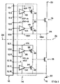
- FIG. 3 shows an exemplary embodiment of an integrated circuit 64 according to the invention which can replace the single transistor 40 from FIG. 1 because it has the required voltage strengths between first terminal 50 and second terminal 52 and first or second terminal 50, 52 and substrate 62.
- the number n of the further transistors is not fixed to the example shown of three further transistors 68, 70 and 72, but may correspond to any integer greater than or equal to 1.
- the integrated circuit 64 has n diodes 74, 76 and 78, each between a Control terminal 80, 82, 84 of the n transistors 68, 70, 72 and a driver supply potential VSH + ⁇ are.
- the driver supply potential corresponds to the potential VSH associated with an additive offset ⁇ at the first connection 50 from FIG. 1, as is provided in FIG.
- a control terminal 86 of the integrated circuit 74 passes either the driver supply potential VSH + ⁇ or the potential VSH at the first terminal 50 to a control terminal 88 of the first transistor 66.
- the integrated circuit 64 has a voltage divider 90 which is parallel to the conductivity paths the transistors 66, 68, 70 and 72 between the first terminal 50 and the second terminal 52 and the control terminals 80, 82, 84, 88 of the further transistors 68, 70, 72 and the first transistor 66 with each other and with the first terminal 50th and the second port 52 connects.
- two control terminals 80, 82, 84, 88 of the transistors 68, 70, 72, 66 are connected to one another via a subsection 92, 94, 96 lying between them.
- Each section 92, 94, 96 has z.
- a resistor 97 as part of the voltage divider 90 provides a connection to the first terminal 50.
- the voltage divider 90 equally distributes the voltage between the first terminal and the second terminal of the integrated circuit to the n transistors 66, 68, 70, 72. As a desired consequence, the voltage across the conductivity path of each individual transistor 66, 68, 70, 72 in FIG turned off state of the circuit 64 is not greater than a permissible maximum value.
- the voltage divider 90 also has a diode 104, which lies between the second terminal 54 and the control terminal 84 of the transistor 72, whose conductivity path also lies on the second terminal 52.
- this diode 104 As a result of the direction-dependent blocking action of this diode 104, a higher voltage can be set at the control terminal 84 of this transistor 72 than at the second terminal 52 of the integrated circuit 64. In this way, the transistor 72 can be switched on independently of the potential at the second connection 52 of the integrated circuit 64.
- the circuit 64 optionally has a decoupling resistor 106 between the control terminal 86 and the control terminal 88 of the first transistor.
- this resistor 106 ensures a potential difference between the control terminal 88 of the first transistor 66 and the control terminal 86 of the integrated circuit 64. This ensures that the first transistor 66 is also opened in the event of an overvoltage.
- the circuit 64 can be switched between two states depending on the potential at the control input 86.
- the driver 44 supplies the potential VSH to the control terminal 86.
- the control terminal 88 of the first transistor 66 sets the same potential VSH as at the first terminal 50 and thus at the source terminal of the first transistor 66. This forms no conductive channel in the first transistor 66, so that the conductivity path of the first transistor 66 and thus also the conductivity path via the other transistors 68, 70, 72 is interrupted.
- the integrated circuit 64 is used instead of the transistor 40 in FIG. 1, the power supply potential from the terminal 20 and at the drain terminal 52 turns on, for example, 16 V higher potential VCP when the conductivity path is interrupted.
- This potential difference of 16 V is uniformly distributed by the voltage divider 90 to the control terminals 88, 80, 82 and 84, so that at the control terminal 88, a potential of 0 V, at the control terminal 80, a potential of about 5 V, at the control terminal 82 a Potential of about 10 V and the control terminal 84 sets a potential of about 15 volts. About 1 V drops across the diode 104.
- the source terminals 108, 110, 112 then set similar potentials, so that at the source terminal 100 on the order of 5 V, the source terminal 110 about 10 V and the source terminal abut about 15 V. D. h., Between the terminals 50 and 52 of the integrated circuit 64 occurring potential difference of z. B. 16 V xxx 66, 68, 70, 72 distributed. Each of the transistors 66, 68, 70, 72 must therefore only a fraction of the Have voltage resistance, which would have to have a single transistor 40 to be used in the circuit arrangement of Figure 1 can. There are no differences between the transistors 66, 68, 70, 72 on the one side and a single transistor 40 on the other side for the voltage resistance between drain and substrate.
- the diodes 74, 76, 78 prevent different potentials at the control terminals 80, 82 and 84 from influencing each other.
- the output of the driver 44 is switched via the terminal 12.5 from the potential VSH to the potential VSH + ⁇ , so that the transistor 88 (in an embodiment as NMOS) conducts , As a result, the potential at terminal 108 decreases so that the control terminal of transistor 68 becomes positive against its source terminal 108. The positive potential at the control terminal 88 turns on the transistor 68. Analogously, the transistors 70 and 72 are turned on, so that a continuous conductive connection between the terminals 50 and 52 via the transistors 66, 68, 70 and 72 results.
- Each of the Zener diodes 114, 116, 118 is parallel to one of the sections 92, 94, 96 of the voltage divider 90, with which control terminals 88, 80, 82, 84 of the transistors 66, 68, 70, 72 are interconnected.
- Zener diodes 114, 116, 118 open a current path which includes the sections 92, 94, 96 of the voltage divider 90 bridged, so that set at the control terminals 88, 80, 82, 84 of the transistors 66, 68, 70, 72 same, opening potentials.
Landscapes
- Semiconductor Integrated Circuits (AREA)
Abstract
Vorgestellt wird eine Integrierte Schaltung (64; 66) mit einem ersten Anschluss (50), einem zweiten Anschluss (52), einem Substrat und einem Steueranschluss (86), wobei der Steueranschluss (86) eine Leitfähigkeit der Integrierten Schaltung (64; 66) zwischen dem ersten Anschluss (50) und dem zweiten Anschluss (52) steuert. Die Integrierte Schaltung (64; 66) zeichnet sich aus durch einen ersten Transistor (66) und n weitere Transistoren (68, 70, 72) mit in Reihe zwischen den ersten Anschluss (50) und den zweiten Anschluss (52) geschalteten Leitfähigkeitsstrecken, wobei n eine ganze Zahl größer oder gleich 1 ist, n Dioden (74, 76, 78), wobei jede der n Dioden (74, 76, 78) zwischen einem Steueranschluss (80, 82, 84) der n Transistoren (68, 70, 72) und einem Treiber-Versorgungspotential (VSH + Δ) liegt, das dem mit einem additiven Offset (Δ) verknüpften Potential (VSH) am ersten Anschluss (50) entspricht, und wobei der Steueranschluss (86) der Integrierten Schaltung (64) entweder das Treiber-Versorgungspotential (VSH + A) oder das Potential (VSH) am ersten Anschluss (50) an einen Steueranschluss (88) des ersten Transistors (66) übergibt, und einen Spannungsteiler (90), der parallel zu den Leitfähigkeitsstrecken zwischen dem ersten Anschluss (50) und dem zweiten Anschluss (52) liegt und der Steueranschlüsse (88, 80, 82, 84) der Transistoren (66, 68, 70, 72) miteinander und mit dem ersten Anschluss (50) sowie dem zweiten Anschluss (52) verbindet, wobei jeweils zwei Steueranschlüsse der Transistoren (66, 68, 70, 72) über einen zwischen ihnen liegenden Teilabschnitt (92, 94, 96) des Spannungsteilers (90) miteinander verbunden sind.

Description
Die Erfindung betrifft eine Integrierte Schaltung mit einem ersten Anschluss, einem zweiten Anschluss, einem Substrat und einem Steueranschluss, wobei der Steueranschluss eine Leitfähigkeit der Integrierten Schaltung zwischen dem ersten und dem zweiten Anschluss steuert.The invention relates to an integrated circuit having a first terminal, a second terminal, a substrate and a control terminal, wherein the control terminal controls a conductivity of the integrated circuit between the first and the second terminal.
Eine solche Integrierte Schaltung entspricht einem Transistor und ist daher bekannt. Bei einer Realisierung der Integrierten Schaltung durch einen einzelnen Feldeffekttransistor wird der erste Anschluss durch den Source-Anschluss, der zweite Anschluss durch den Drain-Anschluss und der Steueranschluss durch den Gate-Anschluss des Feldeffekttransistors definiert. Bei einer Realisierung als Bipolartransistor wird der erste Anschluss z. B. durch den Emitter, der zweite Anschluss durch den Kollektor und der Steueranschluss durch die Basis des Bipolartransistors realisiert.Such an integrated circuit corresponds to a transistor and is therefore known. In a realization of the integrated circuit by a single field effect transistor, the first terminal is defined by the source terminal, the second terminal by the drain terminal and the control terminal by the gate terminal of the field effect transistor. In a realization as a bipolar transistor, the first terminal z. Through the emitter, the second connection through the collector, and the control connection through the base implemented the bipolar transistor.
Je nach Anwendungsfall muss eine solche Integrierte Schaltung, die einen ersten Anschluss, einen zweiten Anschluss, ein Substrat und einen Steueranschluss aufweist, bestimmte Anforderungen für die Spannungsfestigkeit zwischen dem ersten Anschluss und dem zweiten Anschluss auf der einen Seite und dem ersten Anschluss oder dem zweiten Anschluss und dem Substrat auf der anderen Seite erfüllen. Dabei können die innerhalb einer Schaltung geforderten Spannungsfestigkeiten verschieden sein. Bei einem Anwendungsbeispiel einer Schaltung zur Steuerung einer Brückenschaltung aus Leistungstransistoren, wie sie weiter unten noch detaillierter vorgestellt wird, ergeben sich Potentialdifferenzen zwischen dem ersten Anschluss und dem Substrat, die größenordnungsmäßig zwischen - 10 und + 60 V schwanken können. Zusätzlich ergeben sich zwischen dem ersten Anschluss und dem zweiten Anschluss einer solchen Integrierten Schaltung Spannungen von bis zu 20 V, so dass z. B. am zweiten Anschluss der Integrierten Schaltung eine Potentialdifferenz von 20 V + 60 V = 80 V zum Substrat auftreten kann. Diese Anforderungen an die Spannungsfestigkeit zwischen erstem und zweitem Anschluss auf der einen Seite und dem ersten oder zweiten Anschluss und dem Substrat auf der anderen Seite können im Prinzip mit speziell entworfenen Einzeltransistoren erfüllt werden.Depending on the application, such an integrated circuit having a first terminal, a second terminal, a substrate and a control terminal, certain requirements for the dielectric strength between the first terminal and the second terminal on the one side and the first terminal or the second terminal and the substrate on the other side. The required within a circuit voltage strengths may be different. In an application example of a circuit for controlling a bridge circuit of power transistors, as will be described in more detail below, there are potential differences between the first terminal and the substrate, which may vary in magnitude between -10 and + 60V. In addition, arise between the first terminal and the second terminal of such an integrated circuit voltages of up to 20 V, so that z. B. may occur at the second terminal of the integrated circuit, a potential difference of 20 V + 60 V = 80 V to the substrate. These voltage withstand requirements between the first and second terminals on one side and the first or second terminal and the substrate on the other side can, in principle, be met with specially designed single transistors.
Der Entwurf und die Fertigung eines jeweils für spezielle Anforderungen individuell angepassten Einzeltransistors ist jedoch sehr aufwändig. Die Alternative einer Beschränkung der Anwendungsfälle auf solche, die sich durch eine Verwendung vorhandener Einzeltransistoren als Integrierte Schaltungen realisieren lassen, würde die Zahl möglicher Anwendungen unerwünscht einengen.However, the design and manufacture of an individually adapted for each individual requirements individual transistor is very complex. The alternative of limiting the use cases to those that can be realized by using existing single transistors as integrated circuits would undesirably restrict the number of possible applications.
Vor diesem Hintergrund besteht die Aufgabe der Erfindung in der Angabe einer Integrierten Schaltung, die eine Erfiillung der bei verschiedenen Anwendungsfällen verschiedenen Anforderungen an die Spannungsfestigkeit für eine große Zahl von Anwendungsfällen mit einer kleineren Zahl von vorhandenen Transistortypen mit jeweils unterschiedlichen Eigenschaften ermöglicht.Against this background, the object of the invention is to provide an integrated circuit which enables a fulfillment of the voltage stability requirements which are different for different applications for a large number of applications with a smaller number of available transistor types, each with different characteristics.
Diese Aufgabe wird bei einer Integrierten Schaltung der eingangs genannten Art gelöst, die aufweist: Einen ersten Transistor und n weitere Transistoren mit in Reihe zwischen den ersten und den zweiten Anschluss geschalteten Leitfähigkeitsstrecken, wobei n eine ganze Zahl ≥ 1 ist, n Dioden, wobei jede der n Dioden zwischen einem Steueranschluss der n Transistoren und einem Versorgungspotential liegt, das dem mit einem additiven Offset verknüpften Potential am ersten Anschluss entspricht, und wobei der Steueranschluss der Integrierten Schaltung entweder das Versorgungspotential oder das Potential am ersten Anschluss an einen Steueranschluss des ersten Transistors übergibt, und einen Spannungsteiler, der parallel zu den Leitfähigkeitsstrecken zwischen dem ersten Anschluss und dem zweiten Anschluss liegt und der Steueranschlüsse der Transistoren miteinander und mit dem ersten Anschluss sowie dem zweiten Anschluss verbindet, wobei jeweils zwei Steueranschlüsse der Transistoren über einen zwischen ihnen liegenden Teilabschnitt des Spannungsteilers miteinander verbunden sind.This object is achieved in an integrated circuit of the type mentioned in the introduction, comprising: a first transistor and n further transistors with conductivity paths connected in series between the first and the second connection, where n is an integer ≥ 1, n diodes, each the n diodes are connected between a control terminal of the n transistors and a supply potential which corresponds to the potential associated with an additive offset at the first terminal, and wherein the control terminal of the integrated circuit transfers either the supply potential or the potential at the first terminal to a control terminal of the first transistor , And a voltage divider, which is parallel to the conductivity paths between the first terminal and the second terminal and the control terminals of the transistors with each other and connects to the first terminal and the second terminal, wherein in each case two control terminals of the transistors übe r are connected to each other lying between them portion of the voltage divider.
Durch diese Merkmale wird die Aufgabe der Erfindung vollkommen gelöst. Im Einzelnen ergibt sich durch die in Reihe zwischen dem ersten und dem zweiten Anschluss liegenden Leitfähigkeitsstrecken mehrerer Einzeltransistoren eine Spannungsfestigkeit zwischen den genannten Anschlüssen, die der Summe der Spannungsfestigkeiten der verwendeten Einzeltransistoren entspricht. Jeder einzelne der verwendeten Einzeltransistoren muss dann lediglich die geforderte Spannungsfestigkeit zum Substrat besitzen. Die für die gesamte Integrierte Schaltung geforderte Spannungsfestigkeit zwischen dem ersten und zweiten Anschluss lässt sich dann durch die Reihenschaltung mehrerer Leitfähigkeitsstrecken stufenweise beliebig steigern.By these features, the object of the invention is completely solved. In detail, due to the conductivity paths of a plurality of individual transistors lying in series between the first and the second connection, a voltage resistance between the named connections, which corresponds to the sum of the voltage strengths of the individual transistors used, results. Each of the individual transistors used must then have only the required dielectric strength to the substrate. The required for the entire integrated circuit withstand voltage between the first and second terminal can then increase gradually by the series connection of multiple conductivity paths in any order.
Die Dioden sorgen einerseits dafür, dass sich die Steueranschlüsse der Transistoren synchron zueinander in Flussrichtung der Dioden ansteuern lassen. Dadurch werden die Transistoren durch Aktivierung ihrer Leitfähigkeitsstrecken eingeschaltet. Andererseits erlauben die Dioden im ausgeschalteten Zustand der Transistoren die Einstellung verschiedener Gate-Potentiale an den verschiedenen Transistoren ohne wechselseitige Beeinflussung über eine gemeinsame Ansteuerleitung. Dabei werden die Transistoren durch Anlegen des Potentials am ersten Anschluss an den Steueranschluss des ersten Transistors ausgeschaltet und durch Anlegen des Versorgungspotentials an dieser Steueranschluss eingeschaltet.On the one hand, the diodes ensure that the control terminals of the transistors can be driven synchronously in the direction of flow of the diodes. This turns on the transistors by activating their conductivity paths. On the other hand, the diodes in the off state of the transistors allow the setting of different gate potentials at the various transistors without mutual interference via a common drive line. In this case, the transistors are switched off by applying the potential at the first terminal to the control terminal of the first transistor and by Apply the supply potential to this control port turned on.
Im ausgeschalteten Zustand muss dafür gesorgt werden, dass die Spannung über der Leitfähigkeitsstrecke jedes einzelnen Transistors nicht größer als ein zulässiger Maximalwert wird. Dies wird mit Hilfe des Spannungsteilers erreicht, der die Spannung zwischen dem ersten Anschluss und dem zweiten Anschluss der Integrierten Schaltung gleichmäßig auf die n Transistoren verteilt.When switched off, care must be taken to ensure that the voltage across the conductivity path of each individual transistor does not become greater than a permissible maximum value. This is achieved by means of the voltage divider, which distributes the voltage between the first terminal and the second terminal of the integrated circuit equally to the n transistors.
Eine Ausgestaltung der Erfindung zeichnet sich dadurch aus, dass der Spannungsteiler eine Diode aufweist, die zwischen dem zweiten Anschluss der Integrierten Schaltung und dem Steueranschluss des Transistors liegt, dessen Leitfähigkeitsstrecke ebenfalls an dem zweiten Anschluss der Integrierten Schaltung liegt.An embodiment of the invention is characterized in that the voltage divider comprises a diode which is located between the second terminal of the integrated circuit and the control terminal of the transistor whose conductivity path is also at the second terminal of the integrated circuit.
Durch die richtungsabhängige Sperrwirkung dieser Diode lässt sich am Steueranschluss dieses Transistors eine höhere Spannung einstellen als am zweiten Anschluss der Integrierten Schaltung. Dadurch lässt sich dieser Transistor unabhängig vom Potential am zweiten Anschluss der Integrierten Schaltung einschalten.Due to the direction-dependent blocking effect of this diode, a higher voltage can be set at the control terminal of this transistor than at the second terminal of the integrated circuit. As a result, this transistor can be switched on independently of the potential at the second terminal of the integrated circuit.
Eine weitere bevorzugte Ausgestaltung weist eine Reihenschaltung aus n Zenerdioden auf, von denen jede parallel zu einem der Teilabschnitte des Spannungsteilers liegt, mit denen Steueranschlüsse der Transistoren miteinander verbunden sind.A further preferred embodiment has a series connection of n Zener diodes, each of which is parallel to one of the subsections of the voltage divider, with which control terminals of the transistors are connected to one another.
Im Fall einer Überspannung, die bspw. durch eine elektrostatische Entladung zwischen dem ersten und dem zweiten Anschluss der Integrierten Schaltung auftreten kann, öffnen diese Zenerdioden einen Strompfad, der die Teilabschnitte des Spannungsteilers überbrückt, so dass sich an den Steueranschlüssen der Transistoren gleiche, öffnende Potentiale einstellen.In the case of an overvoltage, which can occur, for example, due to an electrostatic discharge between the first and the second terminal of the integrated circuit, these zener diodes open a current path which bridges the sections of the voltage divider, so that equal, opening potentials appear at the control terminals of the transistors to adjust.
Bevorzugt ist auch, dass ein Widerstand zwischen dem Steueranschluss der Integrierten Schaltung und dem Steueranschluss des ersten Transistors angeordnet ist. Im Fall einer Überspannung mit geöffneten Zenerdioden sorgt dieser Widerstand für eine Potentialdifferenz zwischen dem Steueranschluss des ersten Transistors und dem Steueranschluss der Integrierten Schaltung. Dadurch wird gewährleistet, dass auch der erste Transistor im Fall einer Überspannung öffnend angesteuert wird. Durch das öffnende Ansteuern der Transistoren wird eine durchgehende Leitfähigkeitsstrecke zwischen dem ersten Anschluss und dem zweiten Anschluss der Integrierten Schaltung bereitgestellt, über die ein Abbau der Überspannung erfolgen kann.It is also preferable that a resistor is arranged between the control terminal of the integrated circuit and the control terminal of the first transistor. In the case of an overvoltage with open Zener diodes, this resistor provides for a potential difference between the control terminal of the first transistor and the Control connection of the integrated circuit. This ensures that the first transistor is also opened in the event of an overvoltage. By opening the transistors, a continuous conduction path is provided between the first terminal and the second terminal of the integrated circuit, via which the overvoltage can be reduced.
Bevorzugt ist auch, dass die Transistoren als MOS-Feldeffekttransistoren realisiert sind.It is also preferable that the transistors are realized as MOS field-effect transistors.
Solche MOS-Feldeffekttransistoren lassen sich im Gegensatz zu Bipolar-Transistoren kapazitiv und damit nahezu stromlos steuern, was den Stromverbrauch der Integrierten Schaltung verringert. Bei einer solchen Realisierung dienen die Gate-Anschlüsse der Feldeffekttransistoren als Steueranschlüsse. Die Source-Anschlüsse der Feldeffekttransistoren sind zum ersten Anschluss der Integrierten Schaltung gerichtet und die Drain-Anschlüsse sind zum zweiten Anschluss der Integrierten Schaltung gerichtet. Es versteht sich aber, dass die Integrierte Schaltung im Prinzip auch mit Bipolartransistoren realisiert werden kann.In contrast to bipolar transistors, such MOS field-effect transistors can be capacitively and thus virtually currentless, which reduces the power consumption of the integrated circuit. In such an implementation, the gate terminals of the field effect transistors serve as control terminals. The source terminals of the field effect transistors are directed to the first terminal of the integrated circuit and the drain terminals are directed to the second terminal of the integrated circuit. It is understood, however, that the integrated circuit can be realized in principle with bipolar transistors.
Bevorzugt ist auch, dass die Integrierte Schaltung in CMOS-Technik realisiert wird.It is also preferable that the integrated circuit is realized in CMOS technology.
Im Rahmen der CMOS-Technik können bekanntlich n-Kanal- und p-Kanal-Feldeffekttransistoren im gleichen Substrat erzeugt werden. Da n-Kanal- und p-Kanal-Feldeffekttransistoren entgegengesetzt auf gleiche Ansteuersignale reagieren, lassen sich mit einem Ansteuersignal gleichzeitig Einschaltvorgänge und Ausschaltvorgänge steuern.Within the framework of the CMOS technology, it is known that n-channel and p-channel field-effect transistors can be produced in the same substrate. Since n-channel and p-channel field effect transistors react in opposite directions to the same drive signals, it is possible to simultaneously control switch-on operations and switch-off processes with a drive signal.
Eine weitere bevorzugte Ausgestaltung zeichnet sich durch eine Teilschaltung aus, die ein variables Potential an den ersten Anschluss übergibt.A further preferred embodiment is characterized by a subcircuit which transfers a variable potential to the first terminal.
Diese Teilschaltung kann z. B. der untere Teil einer Halbbrücke sein, der an einem niedrigen Versorgungspotential liegt, während die Integrierte Schaltung zwischen dem ersten Anschluss und einem hohen Versorgungspotential liegt. Je nachdem, ob die Integrierte Schaltung oder die Teilschaltung leitfähig gesteuert wird, ergibt sich am Verbindungspunkt der Teilschaltung zur Integrierten Schaltung und damit am ersten Anschluss entweder das niedrige Versorgungspotential oder aber das höhere Versorgungspotential. Auf diese Weise kann z. B. ein Verbraucher, der an den Verbindungspunkt angeschlossen ist, gesteuert werden.This subcircuit can z. B. be the lower part of a half-bridge, which is at a low supply potential, while the integrated circuit is between the first terminal and a high supply potential. Depending on whether the integrated circuit or the subcircuit is conductively controlled, results in the connection point of the subcircuit to the integrated circuit and thus at the first terminal either the low Supply potential or the higher supply potential. In this way, z. For example, a consumer connected to the connection point can be controlled.
Eine weitere bevorzugte Ausgestaltung zeichnet sich durch einen ersten Leistungstransistor aus, dessen Leitfähigkeitsstrecke zwischen dem ersten Anschluss und einer Stromquelle liegt und der durch den zweiten Anschluss gesteuert wird.A further preferred refinement is characterized by a first power transistor whose conductivity path lies between the first terminal and a current source and which is controlled by the second terminal.
Die Integrierte Schaltung wird im Rahmen dieser Ausgestaltung zum Ausschalten des genannten Leistungstransistors verwendet. Wenn die Leitfähigkeitsstrecken der Integrierten Schaltung gesperrt sind, kann durch weitere Schaltungsteile ein Potentialunterschied zwischen Gate und Source des Leistungstransistors eingestellt werden. Werden die Leitfähigkeitsstrecken der Integrierten Schaltung dagegen in den leitenden Zustand gesteuert, so ergeben sich gleiche Potentiale an Gate und Source des Leistungstransistors, wodurch dieser in den sperrenden Zustand gesteuert wird.The integrated circuit is used in the context of this embodiment for switching off said power transistor. If the conductivity paths of the integrated circuit are blocked, a potential difference between the gate and source of the power transistor can be set by further circuit parts. On the other hand, if the conduction paths of the integrated circuit are controlled to the conductive state, equal potentials are produced at the gate and source of the power transistor, thereby controlling them to the blocking state.
Bevorzugt ist auch, dass die Schaltung einen weiteren Leistungstransistor aufweist, dessen Leitfähigkeitsstrecke mit der Leitfähigkeitsstrecke des ersten Leitfähigkeitstransistors in Reihe zwischen der Stromquelle und einem Bezugspotential der Schaltung liegt.It is also preferable that the circuit has a further power transistor whose conductivity path with the conductivity path of the first conductivity transistor is connected in series between the current source and a reference potential of the circuit.
Der weitere Leistungstransistor wird bevorzugt im Wechsel mit dem ersten Leistungstransistor leitend oder sperrend gesteuert, so dass sich am Verbindungspunkt der beiden Leistungstransistoren wechselweise das Potential der Stromquelle oder aber das Bezugspotential einstellt. Auf diese Weise kann ein an dem Verbindungspunkt angeschlossener Verbraucher wechselweise mit beiden Potentialen versorgt werden.The further power transistor is preferably turned on or off in alternation with the first power transistor, so that the potential of the current source or the reference potential alternately sets at the connection point of the two power transistors. In this way, a consumer connected to the connection point can be alternately supplied with both potentials.
Weitere Vorteile ergeben sich aus der Beschreibung und den beigefügten Figuren.Further advantages will become apparent from the description and the accompanying figures.
Es versteht sich, dass die vorstehend genannten und die nachstehend noch zu erläuternden Merkmale nicht nur in der jeweils angegebenen Kombination, sondern auch in anderen Kombinationen oder in Alleinstellung verwendbar sind, ohne den Rahmen der vorliegenden Erfindung zu verlassen.It is understood that the features mentioned above and those yet to be explained below can be used not only in the particular combination given, but also in other combinations or in isolation, without departing from the scope of the present invention.
Ausführungsbeispiele der Erfindung sind in den Zeichnungen dargestellt und werden in der nachfolgenden Beschreibung näher erläutert.Embodiments of the invention are illustrated in the drawings and are explained in more detail in the following description.
Es zeigen:
Figur 1- eine Halbbrücke als Beispiel eines technischen Umfeldes der Erfindung;
- Figur 2
- einen Querschnitt durch einen MOS-Transistor zur Verdeutlichung von Anforderungen an die Spannungsfestigkeit;
- Figur 3
- ein erstes Ausführungsbeispiel der Erfindung mit Beispielwerten von Spannungen, die sich im eingeschalteten Zustand der Integrierten Schaltung ergeben; und
- Figur 4
- ein weiteres Ausführungsbeispiel der Erfindung mit Beispielwerten von Spannungen, die sich im ausgeschalteten Zustand der Integrierten Schaltung einstellen.
- FIG. 1
- a half-bridge as an example of a technical environment of the invention;
- FIG. 2
- a cross section through a MOS transistor to illustrate requirements for the dielectric strength;
- FIG. 3
- a first embodiment of the invention with example values of voltages that result in the switched-on state of the integrated circuit; and
- FIG. 4
- a further embodiment of the invention with example values of voltages that occur in the off state of the integrated circuit.
Figur 1 zeigt eine Halbbrücke 10, die von einer Steuerlogik 12 über eine Ansteuerschaltung 14 gesteuert wird. Die Halbbrücke 10 weist einen ersten Leistungstransistor 16 und einen zweiten Leistungstransistor 18 auf, die in Reihe zwischen einen Leistungsversorgungspotentialanschluss 20 und einen Bezugspotentialanschluss 22 geschaltet sind. Über die Ansteuerschaltung 14 schaltet die Steuerlogik 12 entweder den ersten Leistungstransistor 16 oder den zweiten Leistungstransistor 18 ein. Dazu weist die Steuerlogik 12 Ausgänge 12.1 bis 12.12 auf, die Versorgungsspannungen und/oder Steuersignale ausgeben. Bei eingeschaltetem ersten Leistungstransistor 16 wird der zweite Leistungstransistor 18 ausgeschaltet und umgekehrt. An einem ersten Anschluss 24, der zwischen den beiden Leistungstransistoren 16, 18 liegt, stellt sich daher bei eingeschaltetem zweiten Leistungstransistor 18 das Bezugspotential vom Anschluss 22 ein und bei eingeschaltetem ersten Leistungstransistor 16 stellt sich am ersten Anschluss 24 das Leistungs-Versorgungspotential von Anschluss 20 ein.FIG. 1 shows a half-
Der in der Figur 1 unterhalb des ersten Anschlusses 24 und der Linie 25 liegende Teil der Schaltung mit dem zweiten Leistungstransistor 18 und dem zugehörigen Teil der Ansteuerschaltung 14 stellt damit eine Teilschaltung 26 dar, die ein variables Potential an den ersten Anschluss 24 übergibt. Der zweite Leistungstransistor 18 wird von zwei komplementären Feldeffekttransistoren 28 und 30 gesteuert, die in Reihe zwischen dem Bezugspotentialanschluss 22 und einer Versorgungsspannung VH liegen, die vom Ausgang 12.7 der Steuerlogik 12 ausgegeben wird. In der Figur 1 ist der untere Transistor 28 als N-Kanal-Feldeffekttransistor (NMOS-Fet) und der obere Transistor 30 als P-Kanal-Feldeffekttransistor (PMOS-Fet) realisiert. Ein Treiber 32 steuert einen Steueranschluss 34 des NMOS-Fet 28 in Abhängigkeit von Befehlen der Steuerlogik 12, die über den Ausgang 12.11 ausgegeben werden. Der Treiber 32 legt entweder das am Ausgang 12.12 anliegende Bezugspotential oder ein vom Ausgang 12.10 ausgegebenes Potential VCC auf den Steueranschluss 34, wobei VCC gegenüber dem Bezugspotential positiv ist und den NMOS-Fet 28 einschaltet.The part of the circuit with the
Analog wird der PMOS-Fet 30 durch den Treiber 36 gesteuert, der entweder ein ausschaltendes Potential VH vom Ausgang 12.7 oder ein einschaltendes Potential V_H - Δ vom Ausgang 12.9 auf einen Steueranschluss 38 des PMOS-Fet 30 legt. Der Wert von Δ kann z. B. 5 V betragen. Dabei beziehen sich die Potentiale VCC und VH auf das konstante Bezugspotential am Anschluss 22 der Anordnung, das auch dem Substratpotential der Transistoren 28, 30 entspricht. VCC und VH können typischerweise in einer Größenordnung von etwa 10 V liegen, so dass sich keine hohen Anforderungen an die Spannungsfestigkeit der Transistoren 28, 30 ergeben.Analogously, the PMOS-
Bei den Transistoren 40 und 42, die den ersten Leistungstransistor 16 steuern, ergeben sich dagegen wesentlich höhere Anforderungen an die Spannungsfestigkeit. Bei einer Integration der Schaltung nach Figur 1 auf einem Chip entspricht das Substratpotential dieser Transistoren 40, 42 dem Bezugspotential am Anschluss 22 und ist damit konstant niedrig. Die übrigen Potentiale an Anschlüssen der Transistoren 40, 42 hängen dagegen davon ab, welcher der beiden Leistungstransistoren 16 und 18 eingeschaltet ist. Bei eingeschaltetem zweiten Leistungstransistor 18 und ausgeschaltetem ersten Leistungstransistor 16 stellt sich am ersten Anschluss 24 der Schaltung das Bezugspotential ein. Ist dagegen nur der erste Leistungstransistor 16 eingeschaltet, stellt sich am ersten Anschluss 24 das Leistungs-Versorgungspotential 20 ein. Sämtliche Potentiale, die an Anschlüssen der Transistoren 40, 42 auftreten, basieren auf dem Potential, das sich am ersten Anschluss 24 einstellt. Dadurch werden insbesondere die Potentialunterschiede zum Substratpotential erheblich vergrößert.In the case of the
Der Treiber 44, der den NMOS-Transistor 40 steuert, legt an den Steueranschluss 46 entweder das ausschaltende Potential VSH des ersten Anschlusses 24 oder ein einschaltendes Potential VSH + Δ, das gegenüber VSH positiv ist. Auch hier kann Δ z. B. einen Wert von 5 V besitzen. VSH liegt auch am Anschluss 12.6, während VSH + Δ vom Ausgang 12.4 und das Treiber-Steuersignal vom Anschluss 12.5 ausgegeben wird.The
Analog legt der vom Ausgang 12:2 gesteuerte Treiber 48, der den PMOS-Transistor 42 steuert, an dessen Steueranschluss 49 entweder ein ausschaltendes Potential VCP vom Ausgang 12.1 oder ein einschaltendes Potential VCP - Δ vom Ausgang 12.3. Dabei ist VCP zum Beispiel um 10 V positiver als VSH und VCP - Δ ist um bspw. 5 V negativer als VCP.Analogously, the
Über den Transistor 42 wird der erste Leistungstransistor 16 eingeschaltet und über den Transistor 40 wird der erste Leistungstransistor 16 durch einen Kurzschluss seines Source-Anschlusses 50 und seines Gate-Anschlusses 52 ausgeschaltet. Am ersten Anschluss 50 (Source) des Transistors 40 liegt die Spannung VSH und am zweiten Anschluss 52 (Drain) liegt die Spannung VCP, die den Wert von VCH übersteigt. Der Unterschied zwischen VSH und VCP kann bspw. bis zu 20 V betragen, so dass der Transistor 40 zwischen seinem ersten und seinem zweiten Anschluss, also zwischen Source 50 und Drain 52, entsprechend bis zu 20 V sperren können muss. Da VSH bei eingeschaltetem ersten Leistungstransistor 16 dem Leistungs-Versorgungspotential vom Anschluss 20 entspricht, das bspw. einen Wert von 50 - 60 V besitzt, muss der Transistor 40 mit den angegebenen Werten zwischen Drain 52 und Substrat entsprechend bis zu 80 V sperren können.The
Zur Verdeutlichung dieser Anforderungen an die Spannungsfestigkeit zeigt Figur 2 schematisch einen Querschnitt durch einen n-Kanal MOS-Fet 40. Der MOS-Fet 40 weist einen Substratanschluss 54, einen Source-Anschluss 50, einen Drain-Anschluss 52 und einen Gate-Anschluss 46 über einem Gate-Oxid 56 auf. Im gezeigten Beispiel bildet sich bei hinreichend positivem Gate-Potential ein n-leitender Kanal zwischen n-dotiertem Sourcegebiet 58 und Drain-Gebiet 60 in einem p-leitenden Substrat. Wie in Zusammenhang mit Figur 1 beschrieben wurde, muss der Transistor 40 unter den als Beispiel genannten Umständen eine Spannung von 20 V zwischen Drain und Source sowie eine Spannung von ca. 80 V zwischen Drain und Substrat sperren können.To clarify these voltage stability requirements, FIG. 2 schematically shows a cross section through an n-channel MOS-
Wie eingangs aufgezeigt wurde, kommt es bei der Schaltungsentwicklung hin und wieder vor, dass sich die Anforderungen an die Spannungsfestigkeit mit vorhandenen Bauteilen schlicht und einfach nicht erfüllen lassen. Unter den in Verbindung mit Fig. 1 als Beispiel angegebenen Randbedingungen ist zum Beispiel ein n-Kanaltransistor 40 erforderlich, der zum Substrat 80 V sperren kann und dessen maximale Drain-Source-Spannung größer als 20 V sein muss.As has been shown at the beginning, it sometimes happens during circuit development that the requirements for dielectric strength with existing components simply can not be met. For example, among the constraints given in connection with FIG. 1, an n-
Im Folgenden wird gezeigt, wie sich diese Anforderungen mit anderen Transistoren erfüllen lassen, wenn ein solcher Einzeltransistor nicht zur Verfügung steht.The following shows how these requirements can be met with other transistors if such a single transistor is not available.
Figur 3 zeigt ein Ausführungsbeispiel einer erfindungsgemäßen Integrierten Schaltung 64, die den Einzeltransistor 40 aus Fig. 1 ersetzen kann, weil sie die geforderten Spannungsfestigkeiten zwischen erstem Anschluss 50 und zweitem Anschluss 52 sowie erstem oder zweitem Anschluss 50, 52 und dem Substrat 62 besitzt.FIG. 3 shows an exemplary embodiment of an
Die Integrierte Schaltung 64 weist einen ersten Transistor 66 und n = 3 weitere Transistoren 68, 70 und 72 auf, deren Leitfähigkeitsstrecken in Reihe zwischen dem ersten Anschluss 50 und dem zweiten Anschluss 54 der Integrierten Schaltung 64 liegen. Die Zahl n der weiteren Transistoren ist nicht auf das gezeigte Beispiel von drei weiteren Transistoren 68, 70 und 72 festgelegt, sondern kann jeder ganzen Zahl entsprechen, die größer oder gleich 1 ist. Weiter weist die Integrierte Schaltung 64 n Dioden 74, 76 und 78 auf, die jeweils zwischen einem Steueranschluss 80, 82, 84 der n Transistoren 68, 70, 72 und einem Treiber-Versorgungspotential VSH + Δ liegen. Das Treiber-Versorgungspotential entspricht dem mit einem additiven Offset Δ verknüpften Potential VSH am ersten Anschluss 50 aus Figur 1, wie es in Fig. 1 vom Anschluss 12.4 der Steuerlogik 12 bereitgestellt wird. Ein Steueranschluss 86 der Integrierten Schaltung 74 übergibt entweder das Treiber-Versorgungspotential VSH + Δ oder aber das Potential VSH am ersten Anschluss 50 an einen Steueranschluss 88 des ersten Transistors 66. Weiter weist die Integrierte Schaltung 64 einen Spannungsteiler 90 auf, der parallel zu den Leitfähigkeitsstrecken der Transistoren 66, 68, 70 und 72 zwischen dem ersten Anschluss 50 und dem zweiten Anschluss 52 liegt und der Steueranschlüsse 80, 82, 84, 88 der weiteren Transistoren 68, 70, 72 und des ersten Transistors 66 miteinander und mit dem ersten Anschluss 50 sowie dem zweiten Anschluss 52 verbindet. Dabei sind jeweils zwei Steueranschlüsse 80, 82, 84, 88 der Transistoren 68, 70, 72, 66 über einen zwischen ihnen liegenden Teilabschnitt 92, 94, 96 miteinander verbunden. Jeder Teilabschnitt 92, 94, 96 weist z. B. einen ohmschen Widerstand 98, 100, 102 auf. Ein Widerstand 97 als Teil des Spannungsteilers 90 sorgt für eine Verbindung zum ersten Anschluss 50.The
Der Spannungsteiler 90 verteilt die Spannung zwischen dem ersten Anschluss und dem zweiten Anschluss der Integrierten Schaltung gleichmäßig auf die n Transistoren 66, 68, 70, 72. Als erwünschte Folge wird die Spannung über der Leitfähigkeitsstrecke jedes einzelnen Transistors 66, 68, 70, 72 im ausgeschalteten Zustand der Schaltung 64 nicht größer als ein zulässiger Maximalwert.The
Optional weist der Spannungsteiler 90 noch eine Diode 104 auf, die zwischen dem zweiten Anschluss 54 und dem Steueranschluss 84 des Transistors 72 liegt, dessen Leitfähigkeitsstrecke ebenfalls an dem zweiten Anschluss 52 liegt.Optionally, the
Durch die richtungsabhängige Sperrwirkung dieser Diode 104 lässt sich am Steueranschluss 84 dieses Transistors 72 eine höhere Spannung einstellen als am zweiten Anschluss 52 der Integrierten Schaltung 64. Dadurch lässt sich der Transistor 72 unabhängig vom Potential am zweiten Anschluss 52 der Integrierten Schaltung 64 einschalten.As a result of the direction-dependent blocking action of this
Ferner weist die Schaltung 64 optional einen Entkoppelwiderstand 106 zwischen dem Steueranschluss 86 und dem Steueranschluss 88 des ersten Transistors auf. Im Fall einer Überspannung sorgt dieser Widerstand 106 für eine Potentialdifferenz zwischen dem Steueranschluss 88 des ersten Transistors 66 und dem Steueranschluss 86 der Integrierten Schaltung 64. Dadurch wird gewährleistet, dass auch der erste Transistor 66 im Fall einer Überspannung öffnend angesteuert wird. Durch das öffnende Ansteuern der Transistoren 66, 68, 70, 72 wird eine durchgehende Leitfähigkeitsstrecke zwischen dem ersten Anschluss 50 und dem zweiten Anschluss 52 der Integrierten Schaltung 64 bereitgestellt, über die ein Abbau der Überspannung erfolgen kann.Furthermore, the
Die Schaltung 64 lässt sich in Abhängigkeit vom Potential am Steuereingang 86 zwischen zwei Zuständen umschalten. In einem ersten Zustand liefert der Treiber 44 das Potential VSH an den Steueranschluss 86. Am Steueranschluss 88 des ersten Transistors 66 stellt sich dann das gleiche Potential VSH ein, wie am ersten Anschluss 50 und damit am Source-Anschluss des ersten Transistors 66. Dadurch bildet sich im ersten Transistor 66 kein leitfähiger Kanal aus, so dass die Leitfähigkeitsstrecke des ersten Transistors 66 und damit auch die Leitfähigkeitsstrecke über die übrigen Transistoren 68, 70, 72 unterbrochen ist. Bei einem Einsatz der Integrierten Schaltung 64 anstelle des Transistors 40 in Figur 1 stellt sich bei unterbrochener Leitfähigkeitsstrecke am Source-Anschluss 50 das Leistungs-Versorgungspotential vom Anschluss 20 und am Drain-Anschluss 52 ein um bspw. 16 V höheres Potential VCP ein. Diese Potentialdifferenz von 16 V wird durch den Spannungsteiler 90 gleichmäßig auf die Steueranschlüsse 88, 80, 82 und 84 verteilt, so dass sich am Steueranschluss 88 ein Potential von 0 V, am Steueranschluss 80 ein Potential von ca. 5 V, am Steueranschluss 82 ein Potential von ca. 10 V und am Steueranschluss 84 ein Potential von ca. 15 V einstellt. Etwa 1 V fällt über der Diode 104 ab.The
An den Source-Anschlüssen 108, 110, 112 stellen sich dann ähnliche Potentiale ein, so dass am Source-Anschluss 100 größenordnungsmäßig 5 V, am Source-Anschluss 110 etwa 10 V und am Source-Anschluss etwa 15 V anliegen. D. h., die zwischen den Anschlüssen 50 und 52 der Integrierten Schaltung 64 auftretende Potentialdifferenz von z. B. 16 V xxx 66, 68, 70, 72 verteilt. Jeder einzelne der Transistoren 66, 68, 70, 72 muss daher nur einen Bruchteil der Spannungsfestigkeit aufweisen, die ein einzelner Transistor 40 aufweisen müsste, um in der Schaltungsanordnung nach Figur 1 eingesetzt werden zu können. Für die Anforderungen an die Spannungsfestigkeit zwischen Drain und Substrat ergeben sich keine Unterschiede zwischen den Transistoren 66, 68, 70, 72 auf der einen Seite und einem Einzeltransistor 40 auf der anderen Seite.At the
Die Dioden 74, 76, 78 verhindern, dass sich unterschiedliche Potentiale an den Steueranschlüssen 80, 82 und 84 gegenseitig beeinflussen.The
Um eine leitende Verbindung zwischen den Anschlüssen 50 und 52 der Integrierten Schaltung 64 einzuschalten, wird der Ausgang des Treibers 44 über den Anschluss 12.5 vom Potential VSH auf das Potential VSH + Δ umgeschaltet, so dass der Transistor 88 (bei einer Ausführung als NMOS) leitet. Als Folge sinkt das Potential am Anschluss 108, so dass der Steueranschluss des Transistors 68 positiv gegen seinen Source-Anschluss 108 wird. Das positive Potential am Steueranschluss 88 schaltet den Transistor 68 ein. Analog werden auch die Transistoren 70 und 72 eingeschaltet, so dass sich eine durchgehende leitende Verbindung zwischen den Anschlüssen 50 und 52 über die Transistoren 66, 68, 70 und 72 ergibt.To turn on a conductive connection between the
Fig. 4 zeigt eine Integrierte Schaltung 66, die sich von der Integrierten Schaltung 64 aus Fig. 3 durch eine zusätzliche Reihenschaltung aus n = 3 Zenerdioden 114, 116, 118 unterscheidet. Jede der Zenerdioden 114, 116, 118 liegt parallel zu einem der Teilabschnitte 92, 94, 96 des Spannungsteilers 90 liegt, mit denen Steueranschlüsse 88, 80, 82, 84 der Transistoren 66, 68, 70, 72 miteinander verbunden sind.FIG. 4 shows an
Im Fall einer Überspannung, die bspw. durch eine elektrostatische Entladung zwischen dem ersten Anschluss 50 und dem zweiten Anschluss 52 der Integrierten Schaltung 66 auftreten kann, öffnen diese Zenerdioden 114, 116, 118 einen Strompfad, der die Teilabschnitte 92, 94, 96 des Spannungsteilers 90 überbrückt, so dass sich an den Steueranschlüssen 88, 80, 82, 84 der Transistoren 66, 68, 70, 72 gleiche, öffnende Potentiale einstellen.In the case of an overvoltage, which may occur, for example, due to an electrostatic discharge between the
Claims (9)
der Steueranschluss (86) eine Leitfähigkeit der Integrierten Schaltung (64) zwischen dem ersten Anschluss (50) und dem zweiten Anschluss (52) steuert,
gekennzeichnet durch
einen ersten Transistor (66) und n weitere Transistoren (68, 70, 72) mit in Reihe zwischen den ersten Anschluss (50) und den zweiten Anschluss (52) geschalteten Leitfähigkeitsstrecken, wobei n eine ganze Zahl größer oder gleich 1 ist,
n Dioden (74, 76, 78), wobei jede der n Dioden (74, 76, 78) zwischen einem Steueranschluss (80, 82, 84) der n Transistoren (68, 70, 72) und einem Treiber-Versorgungspotential (VSH + Δ) liegt, das dem mit einem additiven Offset (Δ) verknüpften Potential (VSH) am ersten Anschluss (50) entspricht, und wobei der Steueranschluss (86) der Integrierten Schaltung (64) entweder das Treiber-Versorgungspotential (VSH + Δ) oder das Potential (VSH) am ersten Anschluss (50) an einen Steueranschluss (88) des ersten Transistors (66) übergibt, und
einen Spannungsteiler (90), der parallel zu den Leitfähigkeitsstrecken zwischen dem ersten Anschluss (50) und dem zweiten Anschluss (52) liegt und der Steueranschlüsse (88, 80, 82, 84) der Transistoren (66, 68, 70, 72) miteinander und mit dem ersten Anschluss (50) sowie dem zweiten Anschluss (52) verbindet, wobei jeweils zwei Steueranschlüsse der Transistoren (66, 68, 70, 72) über einen zwischen ihnen liegenden Teilabschnitt (92, 94, 96) des Spannungsteilers (90) miteinander verbunden sind.An integrated circuit (64) having a first terminal (50), a second terminal (52), a substrate (62) and a control terminal (86), wherein
the control port controls a conductivity of the integrated circuit between the first port and the second port;
marked by
a first transistor (66) and n further transistors (68, 70, 72) having conductivity paths connected in series between the first port (50) and the second port (52), where n is an integer greater than or equal to 1,
n diodes (74, 76, 78), each of the n diodes (74, 76, 78) being connected between a control terminal (80, 82, 84) of the n transistors (68, 70, 72) and a driver supply potential (VSH + Δ) corresponding to the potential (VSH) associated with an additive offset (Δ) at the first terminal (50), and wherein the control terminal (86) of the integrated circuit (64) has either the driver supply potential (VSH + Δ) or the potential (VSH) at the first terminal (50) to a control terminal (88) of the first transistor (66) passes, and
a voltage divider (90) which is in parallel with the conduction paths between the first terminal (50) and the second terminal (52) and the control terminals (88, 80, 82, 84) of the transistors (66, 68, 70, 72) with each other and with the first terminal (50) and the second terminal (52), wherein in each case two control terminals of the transistors (66, 68, 70, 72) via a lying between them portion (92, 94, 96) of the voltage divider (90) connected to each other.
Applications Claiming Priority (1)
| Application Number | Priority Date | Filing Date | Title |
|---|---|---|---|
| DE102004039620A DE102004039620B4 (en) | 2004-08-06 | 2004-08-06 | Integrated circuit, which has a predetermined dielectric strength |
Publications (1)
| Publication Number | Publication Date |
|---|---|
| EP1624572A1 true EP1624572A1 (en) | 2006-02-08 |
Family
ID=35311474
Family Applications (1)
| Application Number | Title | Priority Date | Filing Date |
|---|---|---|---|
| EP05016720A Withdrawn EP1624572A1 (en) | 2004-08-06 | 2005-08-02 | Integrated circuit with a specified withstand voltage |
Country Status (3)
| Country | Link |
|---|---|
| US (1) | US7619252B2 (en) |
| EP (1) | EP1624572A1 (en) |
| DE (1) | DE102004039620B4 (en) |
Cited By (1)
| Publication number | Priority date | Publication date | Assignee | Title |
|---|---|---|---|---|
| WO2011022551A1 (en) * | 2009-08-19 | 2011-02-24 | Qualcomm Incorporated | Stacked amplifier with diode-based biasing |
Families Citing this family (3)
| Publication number | Priority date | Publication date | Assignee | Title |
|---|---|---|---|---|
| EP2293445B1 (en) * | 2009-08-26 | 2013-03-06 | The Alfred E. Mann Foundation for Scientific Research | High voltage current source and voltage expander in low voltage process |
| US9831764B2 (en) * | 2014-11-20 | 2017-11-28 | Stmicroelectronics International N.V. | Scalable protection voltage generator |
| CN110825148B (en) * | 2019-10-30 | 2021-06-04 | 新鸿电子有限公司 | Constant current control power supply circuit and field emission electron source |
Citations (5)
| Publication number | Priority date | Publication date | Assignee | Title |
|---|---|---|---|---|
| DE3100795A1 (en) * | 1980-07-09 | 1982-08-05 | Siemens AG, 1000 Berlin und 8000 München | Switch with series-connected field-effect transistors |
| JPS60247325A (en) * | 1984-05-23 | 1985-12-07 | Hitachi Ltd | switch circuit |
| US4751408A (en) * | 1985-09-06 | 1988-06-14 | Thomson-Csf | Voltage-switching device |
| US6320362B1 (en) * | 1999-11-26 | 2001-11-20 | Korea Electrotechnology Research Institute | Passive auxiliary circuit for series connection of a power switch |
| US6380793B1 (en) * | 1999-10-28 | 2002-04-30 | Pixtech S.A. | Very high voltage switch |
Family Cites Families (9)
| Publication number | Priority date | Publication date | Assignee | Title |
|---|---|---|---|---|
| BE792285A (en) * | 1971-12-06 | 1973-06-05 | Xerox Corp | CURRENT REGULATION CIRCUITS |
| US4367421A (en) * | 1980-04-21 | 1983-01-04 | Reliance Electric Company | Biasing methods and circuits for series connected transistor switches |
| DE3026040C2 (en) * | 1980-07-09 | 1982-05-27 | Siemens AG, 1000 Berlin und 8000 München | Switch with MOS-FET connected in series |
| DE3522429A1 (en) * | 1985-06-22 | 1987-01-02 | Bosch Gmbh Robert | CIRCUIT ARRANGEMENT FOR THE DRIVER CIRCUIT OF HIGH VOLTAGE POWER TRANSISTORS |
| US4751480A (en) * | 1986-11-14 | 1988-06-14 | Hewlett-Packard Company | One port magnetostatic wave resonator |
| US5382826A (en) * | 1993-12-21 | 1995-01-17 | Xerox Corporation | Stacked high voltage transistor unit |
| JP3485655B2 (en) * | 1994-12-14 | 2004-01-13 | 株式会社ルネサステクノロジ | Composite MOSFET |
| US6429492B1 (en) * | 1999-06-23 | 2002-08-06 | Bae Systems Information And Electronic Systems Integration, Inc. | Low-power CMOS device and logic gates/circuits therewith |
| US6836148B2 (en) * | 2002-04-08 | 2004-12-28 | Texas Instruments Incorporated | Versatile high voltage outputs using low voltage transistors |
-
2004
- 2004-08-06 DE DE102004039620A patent/DE102004039620B4/en not_active Expired - Fee Related
-
2005
- 2005-08-02 EP EP05016720A patent/EP1624572A1/en not_active Withdrawn
- 2005-08-04 US US11/196,277 patent/US7619252B2/en not_active Expired - Fee Related
Patent Citations (5)
| Publication number | Priority date | Publication date | Assignee | Title |
|---|---|---|---|---|
| DE3100795A1 (en) * | 1980-07-09 | 1982-08-05 | Siemens AG, 1000 Berlin und 8000 München | Switch with series-connected field-effect transistors |
| JPS60247325A (en) * | 1984-05-23 | 1985-12-07 | Hitachi Ltd | switch circuit |
| US4751408A (en) * | 1985-09-06 | 1988-06-14 | Thomson-Csf | Voltage-switching device |
| US6380793B1 (en) * | 1999-10-28 | 2002-04-30 | Pixtech S.A. | Very high voltage switch |
| US6320362B1 (en) * | 1999-11-26 | 2001-11-20 | Korea Electrotechnology Research Institute | Passive auxiliary circuit for series connection of a power switch |
Non-Patent Citations (1)
| Title |
|---|
| PATENT ABSTRACTS OF JAPAN vol. 010, no. 113 (E - 399) 26 April 1986 (1986-04-26) * |
Cited By (2)
| Publication number | Priority date | Publication date | Assignee | Title |
|---|---|---|---|---|
| WO2011022551A1 (en) * | 2009-08-19 | 2011-02-24 | Qualcomm Incorporated | Stacked amplifier with diode-based biasing |
| US8847689B2 (en) | 2009-08-19 | 2014-09-30 | Qualcomm Incorporated | Stacked amplifier with diode-based biasing |
Also Published As
| Publication number | Publication date |
|---|---|
| US20060028263A1 (en) | 2006-02-09 |
| DE102004039620B4 (en) | 2006-10-12 |
| DE102004039620A1 (en) | 2006-03-16 |
| US7619252B2 (en) | 2009-11-17 |
Similar Documents
| Publication | Publication Date | Title |
|---|---|---|
| DE69808244T2 (en) | HIGH VOLTAGE CMOS LEVEL CONVERTER | |
| DE69927663T2 (en) | Over or under voltage tolerant transfer gate | |
| DE102016114820A1 (en) | System and method for a switch with a normally-on transistor and a normally-off transistor | |
| DE112017003652T5 (en) | Hybrid switch with GaN HEMT and MOSFET | |
| DE102015104946B4 (en) | Electronic driver circuit and method | |
| DE102006029474A1 (en) | Cascode circuit for driving high electron mobility transistor, has controller that controls low voltage MOSFET for faster charging of capacitor | |
| EP2412096A2 (en) | Switching device having a cascode circuit | |
| DE10344572A1 (en) | Gate control device for reducing surge voltage and switching loss | |
| DE102015114371A1 (en) | SYSTEM AND METHOD FOR A SWITCH WITH A SELF-LEADING TRANSISTOR AND A TRANSISTOR LOCKING TRANSISTOR | |
| EP1887698A2 (en) | Level shift for an actuator switch for high performance semiconductor components | |
| DE102014108576A1 (en) | Driver circuit with Miller-Clamping functionality for power semiconductor switch, power semiconductor switch and inverter bridge | |
| DE102016112814A1 (en) | System and method for a switching transistor | |
| EP0130587A2 (en) | Input level converter for a digital MOS circuit | |
| DE2712742A1 (en) | FIELD EFFECT TRANSISTOR CIRCUIT | |
| EP1094605B1 (en) | Circuit arrangement for controlling a load with reduced stray radiation | |
| EP0637874B1 (en) | MOS switching stage | |
| DE3904910C2 (en) | ||
| DE102004039620B4 (en) | Integrated circuit, which has a predetermined dielectric strength | |
| DE69112153T2 (en) | Level converter with individual control and low dynamic impedance. | |
| EP3918713A1 (en) | Circuit assembly for controlling an inverter | |
| DE69502057T2 (en) | Control circuit for a bias voltage source | |
| DE102004004270B3 (en) | Integrated power switching circuit compares gate voltage of power MOS transistor with reference voltage and provides disabling output that disables one of series-connected transistors, when gate voltage reaches reference voltage | |
| EP2458737A1 (en) | Diode replacement circuit and step-up converter circuit, step-down converter circuit and bridge rectifier circuit respectively comprising the same | |
| WO2019063308A1 (en) | OPTIMIZED CASCODE HALF BRIDGE | |
| WO2004064232A2 (en) | Voltage supply circuit and method for generating a supply voltage |
Legal Events
| Date | Code | Title | Description |
|---|---|---|---|
| PUAI | Public reference made under article 153(3) epc to a published international application that has entered the european phase |
Free format text: ORIGINAL CODE: 0009012 |
|
| 17P | Request for examination filed |
Effective date: 20050802 |
|
| AK | Designated contracting states |
Kind code of ref document: A1 Designated state(s): AT BE BG CH CY CZ DE DK EE ES FI FR GB GR HU IE IS IT LI LT LU LV MC NL PL PT RO SE SI SK TR |
|
| AX | Request for extension of the european patent |
Extension state: AL BA HR MK YU |
|
| AKX | Designation fees paid |
Designated state(s): DE FR |
|
| STAA | Information on the status of an ep patent application or granted ep patent |
Free format text: STATUS: THE APPLICATION HAS BEEN WITHDRAWN |
|
| 18W | Application withdrawn |
Effective date: 20080815 |