EP1491884A1 - Biosensor and method of preparation - Google Patents
Biosensor and method of preparation Download PDFInfo
- Publication number
- EP1491884A1 EP1491884A1 EP20030253999 EP03253999A EP1491884A1 EP 1491884 A1 EP1491884 A1 EP 1491884A1 EP 20030253999 EP20030253999 EP 20030253999 EP 03253999 A EP03253999 A EP 03253999A EP 1491884 A1 EP1491884 A1 EP 1491884A1
- Authority
- EP
- European Patent Office
- Prior art keywords
- silicon substrate
- compounds
- target
- target portion
- target portions
- Prior art date
- Legal status (The legal status is an assumption and is not a legal conclusion. Google has not performed a legal analysis and makes no representation as to the accuracy of the status listed.)
- Withdrawn
Links
- 238000000034 method Methods 0.000 title claims description 49
- 150000001875 compounds Chemical class 0.000 claims abstract description 98
- XUIMIQQOPSSXEZ-UHFFFAOYSA-N Silicon Chemical compound [Si] XUIMIQQOPSSXEZ-UHFFFAOYSA-N 0.000 claims abstract description 75
- 229910052710 silicon Inorganic materials 0.000 claims abstract description 75
- 239000010703 silicon Substances 0.000 claims abstract description 75
- 239000000758 substrate Substances 0.000 claims abstract description 55
- 239000000126 substance Substances 0.000 claims abstract description 53
- 239000002356 single layer Substances 0.000 claims abstract description 48
- VYPSYNLAJGMNEJ-UHFFFAOYSA-N Silicium dioxide Chemical compound O=[Si]=O VYPSYNLAJGMNEJ-UHFFFAOYSA-N 0.000 claims abstract description 39
- 239000000203 mixture Substances 0.000 claims abstract description 37
- 239000010410 layer Substances 0.000 claims abstract description 26
- 230000005855 radiation Effects 0.000 claims abstract description 20
- 229920001542 oligosaccharide Polymers 0.000 claims abstract description 19
- 150000002482 oligosaccharides Chemical class 0.000 claims abstract description 19
- 108010038807 Oligopeptides Chemical class 0.000 claims abstract description 17
- 102000015636 Oligopeptides Human genes 0.000 claims abstract description 17
- 229910052760 oxygen Inorganic materials 0.000 claims abstract description 15
- QVGXLLKOCUKJST-UHFFFAOYSA-N atomic oxygen Chemical compound [O] QVGXLLKOCUKJST-UHFFFAOYSA-N 0.000 claims abstract description 14
- 239000001301 oxygen Substances 0.000 claims abstract description 14
- 238000004519 manufacturing process Methods 0.000 claims abstract description 13
- 230000001678 irradiating effect Effects 0.000 claims abstract description 9
- 229910052814 silicon oxide Inorganic materials 0.000 claims abstract description 9
- 230000005669 field effect Effects 0.000 claims abstract description 6
- 229910052739 hydrogen Inorganic materials 0.000 claims abstract description 6
- 239000001257 hydrogen Substances 0.000 claims abstract description 6
- 125000004450 alkenylene group Chemical group 0.000 claims abstract description 5
- 125000004419 alkynylene group Chemical group 0.000 claims abstract description 5
- 230000008878 coupling Effects 0.000 claims abstract 2
- 238000010168 coupling process Methods 0.000 claims abstract 2
- 238000005859 coupling reaction Methods 0.000 claims abstract 2
- 125000006239 protecting group Chemical group 0.000 claims description 6
- 229910052736 halogen Inorganic materials 0.000 claims description 5
- 150000002367 halogens Chemical class 0.000 claims description 5
- 125000004435 hydrogen atom Chemical group [H]* 0.000 claims description 4
- 125000004149 thio group Chemical group *S* 0.000 claims description 4
- XFXPMWWXUTWYJX-UHFFFAOYSA-N Cyanide Chemical group N#[C-] XFXPMWWXUTWYJX-UHFFFAOYSA-N 0.000 claims description 3
- 125000003545 alkoxy group Chemical group 0.000 claims description 3
- 150000001408 amides Chemical class 0.000 claims description 3
- 150000001412 amines Chemical class 0.000 claims description 3
- 150000001732 carboxylic acid derivatives Chemical class 0.000 claims description 3
- 150000002148 esters Chemical class 0.000 claims description 3
- 125000002887 hydroxy group Chemical class [H]O* 0.000 claims description 3
- 125000000391 vinyl group Chemical group [H]C([*])=C([H])[H] 0.000 claims description 3
- UFHFLCQGNIYNRP-UHFFFAOYSA-N Hydrogen Chemical compound [H][H] UFHFLCQGNIYNRP-UHFFFAOYSA-N 0.000 claims description 2
- 150000001720 carbohydrates Chemical group 0.000 claims 1
- 150000001336 alkenes Chemical class 0.000 abstract description 4
- 150000001345 alkine derivatives Chemical class 0.000 abstract description 2
- 229910052799 carbon Inorganic materials 0.000 abstract 1
- 239000012044 organic layer Substances 0.000 abstract 1
- 229910052717 sulfur Inorganic materials 0.000 abstract 1
- 238000006243 chemical reaction Methods 0.000 description 22
- 125000001424 substituent group Chemical group 0.000 description 18
- 125000005647 linker group Chemical group 0.000 description 16
- 229910052681 coesite Inorganic materials 0.000 description 15
- 229910052906 cristobalite Inorganic materials 0.000 description 15
- 239000000377 silicon dioxide Substances 0.000 description 15
- 229910052682 stishovite Inorganic materials 0.000 description 15
- 229910052905 tridymite Inorganic materials 0.000 description 15
- 238000012360 testing method Methods 0.000 description 7
- 238000005530 etching Methods 0.000 description 6
- 125000000217 alkyl group Chemical group 0.000 description 5
- 230000015572 biosynthetic process Effects 0.000 description 5
- 230000008569 process Effects 0.000 description 5
- 230000035945 sensitivity Effects 0.000 description 5
- 239000002555 ionophore Substances 0.000 description 4
- 230000000236 ionophoric effect Effects 0.000 description 4
- 239000012528 membrane Substances 0.000 description 4
- 239000013638 trimer Substances 0.000 description 4
- 150000001335 aliphatic alkanes Chemical class 0.000 description 3
- 125000002947 alkylene group Chemical group 0.000 description 3
- 239000003792 electrolyte Substances 0.000 description 3
- 150000002500 ions Chemical class 0.000 description 3
- 230000004044 response Effects 0.000 description 3
- SQVRNKJHWKZAKO-OQPLDHBCSA-N sialic acid Chemical compound CC(=O)N[C@@H]1[C@@H](O)C[C@@](O)(C(O)=O)OC1[C@H](O)[C@H](O)CO SQVRNKJHWKZAKO-OQPLDHBCSA-N 0.000 description 3
- 0 *C(CO)(CC1)C([C@@]([C@@](CO)O)O)O[C@]1(C(O)=O)OC(C(C(CO)OC1OC(C(CO)OC(C2O)O)C2O)O)C1O Chemical compound *C(CO)(CC1)C([C@@]([C@@](CO)O)O)O[C@]1(C(O)=O)OC(C(C(CO)OC1OC(C(CO)OC(C2O)O)C2O)O)C1O 0.000 description 2
- CURLTUGMZLYLDI-UHFFFAOYSA-N Carbon dioxide Chemical compound O=C=O CURLTUGMZLYLDI-UHFFFAOYSA-N 0.000 description 2
- YXFVVABEGXRONW-UHFFFAOYSA-N Toluene Natural products CC1=CC=CC=C1 YXFVVABEGXRONW-UHFFFAOYSA-N 0.000 description 2
- 125000004429 atom Chemical group 0.000 description 2
- 230000008901 benefit Effects 0.000 description 2
- 238000011161 development Methods 0.000 description 2
- 230000018109 developmental process Effects 0.000 description 2
- 239000008151 electrolyte solution Substances 0.000 description 2
- 238000010438 heat treatment Methods 0.000 description 2
- 239000011229 interlayer Substances 0.000 description 2
- GUBGYTABKSRVRQ-QKKXKWKRSA-N lactose group Chemical group OC1[C@H](O)[C@@H](O)[C@H](O[C@H]2[C@H](O)[C@@H](O)[C@@H](O)[C@H](O2)CO)[C@H](O1)CO GUBGYTABKSRVRQ-QKKXKWKRSA-N 0.000 description 2
- 239000007800 oxidant agent Substances 0.000 description 2
- 238000000059 patterning Methods 0.000 description 2
- 239000011241 protective layer Substances 0.000 description 2
- 102000004169 proteins and genes Human genes 0.000 description 2
- 108090000623 proteins and genes Proteins 0.000 description 2
- 125000005630 sialyl group Chemical group 0.000 description 2
- 208000011580 syndromic disease Diseases 0.000 description 2
- 150000004043 trisaccharides Chemical class 0.000 description 2
- GUBGYTABKSRVRQ-XLOQQCSPSA-N Alpha-Lactose Chemical group O[C@@H]1[C@@H](O)[C@@H](O)[C@@H](CO)O[C@H]1O[C@@H]1[C@@H](CO)O[C@H](O)[C@H](O)[C@H]1O GUBGYTABKSRVRQ-XLOQQCSPSA-N 0.000 description 1
- 241000894006 Bacteria Species 0.000 description 1
- WQZGKKKJIJFFOK-GASJEMHNSA-N Glucose Natural products OC[C@H]1OC(O)[C@H](O)[C@@H](O)[C@@H]1O WQZGKKKJIJFFOK-GASJEMHNSA-N 0.000 description 1
- 229910052581 Si3N4 Inorganic materials 0.000 description 1
- 241000700605 Viruses Species 0.000 description 1
- JRQOTZAJQMBWJY-RJMJUYIDSA-N acetic acid (2R,3R,4S,5R,6S)-2-(hydroxymethyl)-6-[(2R,3S,4R,5R)-4,5,6-trihydroxy-2-(hydroxymethyl)oxan-3-yl]oxyoxane-3,4,5-triol Chemical compound CC(O)=O.O[C@@H]1[C@@H](O)[C@@H](O)[C@@H](CO)O[C@H]1O[C@H]1[C@H](O)[C@@H](O)C(O)O[C@@H]1CO JRQOTZAJQMBWJY-RJMJUYIDSA-N 0.000 description 1
- 239000002253 acid Substances 0.000 description 1
- 230000002378 acidificating effect Effects 0.000 description 1
- 125000002355 alkine group Chemical group 0.000 description 1
- PNEYBMLMFCGWSK-UHFFFAOYSA-N aluminium oxide Inorganic materials [O-2].[O-2].[O-2].[Al+3].[Al+3] PNEYBMLMFCGWSK-UHFFFAOYSA-N 0.000 description 1
- SQVRNKJHWKZAKO-UHFFFAOYSA-N beta-N-Acetyl-D-neuraminic acid Natural products CC(=O)NC1C(O)CC(O)(C(O)=O)OC1C(O)C(O)CO SQVRNKJHWKZAKO-UHFFFAOYSA-N 0.000 description 1
- 239000008280 blood Substances 0.000 description 1
- 210000004369 blood Anatomy 0.000 description 1
- 229910002092 carbon dioxide Inorganic materials 0.000 description 1
- 239000001569 carbon dioxide Substances 0.000 description 1
- 125000003178 carboxy group Chemical group [H]OC(*)=O 0.000 description 1
- 229940126214 compound 3 Drugs 0.000 description 1
- 229910052593 corundum Inorganic materials 0.000 description 1
- 238000000151 deposition Methods 0.000 description 1
- 238000001514 detection method Methods 0.000 description 1
- 239000012470 diluted sample Substances 0.000 description 1
- 239000000539 dimer Substances 0.000 description 1
- 230000000694 effects Effects 0.000 description 1
- 230000005684 electric field Effects 0.000 description 1
- 125000000524 functional group Chemical group 0.000 description 1
- 239000008103 glucose Substances 0.000 description 1
- 230000000977 initiatory effect Effects 0.000 description 1
- 230000003993 interaction Effects 0.000 description 1
- 239000008101 lactose Substances 0.000 description 1
- 238000001459 lithography Methods 0.000 description 1
- 239000000463 material Substances 0.000 description 1
- 230000004048 modification Effects 0.000 description 1
- 238000012986 modification Methods 0.000 description 1
- 239000003960 organic solvent Substances 0.000 description 1
- 230000003647 oxidation Effects 0.000 description 1
- 238000007254 oxidation reaction Methods 0.000 description 1
- 238000012856 packing Methods 0.000 description 1
- 229920000642 polymer Polymers 0.000 description 1
- 230000001681 protective effect Effects 0.000 description 1
- 230000035484 reaction time Effects 0.000 description 1
- 230000009467 reduction Effects 0.000 description 1
- 210000002966 serum Anatomy 0.000 description 1
- SCPYDCQAZCOKTP-UHFFFAOYSA-N silanol Chemical compound [SiH3]O SCPYDCQAZCOKTP-UHFFFAOYSA-N 0.000 description 1
- 125000005372 silanol group Chemical group 0.000 description 1
- 239000000243 solution Substances 0.000 description 1
- 239000002904 solvent Substances 0.000 description 1
- 239000007858 starting material Substances 0.000 description 1
- 238000003786 synthesis reaction Methods 0.000 description 1
- PBCFLUZVCVVTBY-UHFFFAOYSA-N tantalum pentoxide Inorganic materials O=[Ta](=O)O[Ta](=O)=O PBCFLUZVCVVTBY-UHFFFAOYSA-N 0.000 description 1
- 125000003944 tolyl group Chemical group 0.000 description 1
- 238000006257 total synthesis reaction Methods 0.000 description 1
- XLYOFNOQVPJJNP-UHFFFAOYSA-N water Substances O XLYOFNOQVPJJNP-UHFFFAOYSA-N 0.000 description 1
- 229910001845 yogo sapphire Inorganic materials 0.000 description 1
Images


Classifications
-
- G—PHYSICS
- G01—MEASURING; TESTING
- G01N—INVESTIGATING OR ANALYSING MATERIALS BY DETERMINING THEIR CHEMICAL OR PHYSICAL PROPERTIES
- G01N33/00—Investigating or analysing materials by specific methods not covered by groups G01N1/00 - G01N31/00
- G01N33/48—Biological material, e.g. blood, urine; Haemocytometers
- G01N33/50—Chemical analysis of biological material, e.g. blood, urine; Testing involving biospecific ligand binding methods; Immunological testing
- G01N33/53—Immunoassay; Biospecific binding assay; Materials therefor
- G01N33/543—Immunoassay; Biospecific binding assay; Materials therefor with an insoluble carrier for immobilising immunochemicals
- G01N33/54366—Apparatus specially adapted for solid-phase testing
- G01N33/54373—Apparatus specially adapted for solid-phase testing involving physiochemical end-point determination, e.g. wave-guides, FETS, gratings
- G01N33/5438—Electrodes
-
- G—PHYSICS
- G01—MEASURING; TESTING
- G01N—INVESTIGATING OR ANALYSING MATERIALS BY DETERMINING THEIR CHEMICAL OR PHYSICAL PROPERTIES
- G01N27/00—Investigating or analysing materials by the use of electric, electrochemical, or magnetic means
- G01N27/26—Investigating or analysing materials by the use of electric, electrochemical, or magnetic means by investigating electrochemical variables; by using electrolysis or electrophoresis
- G01N27/403—Cells and electrode assemblies
- G01N27/414—Ion-sensitive or chemical field-effect transistors, i.e. ISFETS or CHEMFETS
- G01N27/4145—Ion-sensitive or chemical field-effect transistors, i.e. ISFETS or CHEMFETS specially adapted for biomolecules, e.g. gate electrode with immobilised receptors
-
- Y—GENERAL TAGGING OF NEW TECHNOLOGICAL DEVELOPMENTS; GENERAL TAGGING OF CROSS-SECTIONAL TECHNOLOGIES SPANNING OVER SEVERAL SECTIONS OF THE IPC; TECHNICAL SUBJECTS COVERED BY FORMER USPC CROSS-REFERENCE ART COLLECTIONS [XRACs] AND DIGESTS
- Y10—TECHNICAL SUBJECTS COVERED BY FORMER USPC
- Y10S—TECHNICAL SUBJECTS COVERED BY FORMER USPC CROSS-REFERENCE ART COLLECTIONS [XRACs] AND DIGESTS
- Y10S977/00—Nanotechnology
- Y10S977/70—Nanostructure
- Y10S977/788—Of specified organic or carbon-based composition
- Y10S977/809—Organic film on silicon
Definitions
- the present invention relates to a device manufacturing method for the production of silicon substrates having functionalised surfaces, as well as devices manufactured thereby.
- the invention also relates, in particular, to devices which can be employed as chemical or biological sensors.
- the silicon surface with its inherent protective layer of SiO 2 , provides the base for the ability to structure and modify silicon surfaces to form integrated circuits (ICs).
- ICs integrated circuits
- the field of use of integrated circuits could be significantly extended, however, if functionality could be introduced on the basic silicon substrate. In particular, there is a desire to introduce biological functionality. To extend the suitability of silicon for such new uses, techniques are needed which enable a wide variety of different functionalities to be added to the silicon surface.
- a difficulty which has been envisaged with such new techniques is the potential damage to the SiO 2 layer which naturally covers the silicon surface.
- the SiO 2 layer inherently protects the underlying silicon substrate and any modification which causes a reduction in this protective effect is therefore to be avoided.
- FET field effect transistor
- the Ion Sensitive Field Effect Transistor is a simple example of a known FET-based chemical sensor.
- the silicon oxide which covers the gate area of an FET also serves as a chemical sensor.
- an electrolyte is in electrical contact with the oxide gate.
- a different proportion of the silanol sites on the oxide surface will be protonated.
- silanol groups at the surface may be protonated or deprotonated, causing an interface potential to form at the oxide/electrolyte junction.
- This interface potential directly affects the electric field in the oxide and thus the channel resistance in the FET device. In this way, the FET senses the pH of the electrolyte solution.
- These devices show a very fast response to changes in pH. Further, the selectivity and sensitivity of the sensor can be controlled by changing the substance that is used as the gate.
- Al 2 O 3 , Si 3 N 4 and Ta 2 O 5 are examples of suitable materials which can be used as an alternative to the usual SiO 2 .
- ISFET devices are inherently applicable only to the detection of changes in pH. Further development was therefore needed to provide sensors with increased applicability. Changing the ISFET into a sensor which can detect other ions was expected initially to be possible simply by depositing PVC membranes containing ionophores directly onto the gate oxide of the FET. However, such structures were found to be unstable and sensitive to carbon dioxide and were therefore not suitable for practical use. To solve these difficulties, an additional interlayer was incorporated between the PVC membrane and the oxide gate, leading to the device known as a ChemFET. ChemFETs can be designed to be selective for a variety of different ions, depending on the ionophore incorporated into the PVC membrane. Polymeric membranes can also be used incorporating molecular receptors. ChemFETs therefore have a very wide application in the field of chemical sensors. A description of a recent ChemFET device is found in European Patent Application No. 02076942.8, which is incorporated herein in its entirety.
- ChemFETs have various drawbacks.
- the use of the additional interlayer leads to a sensor reaction time which is significantly slower than the original ISFET.
- ChemFETs also have a limited sensitivity and therefore the signal to noise ratio can be unfavourable. These types of device are therefore not suitable for use with very small volumes of test substance of highly diluted samples.
- ChemFETs are complicated by the need to attach all layers to one another by covalent or ionic bonding.
- the individual layers must therefore each contain surface active groups from which suitable bonds can be formed, as well as the desired sensing ionophores and any other required functional groups.
- a new sensor is therefore desired which has the rapid response of the original ISFET device but can be adapted to test for a variety of different substances.
- any new sensor should desirably be compatible with biological systems so that it can be used to test for the presence of specific proteins or other biological substances.
- the sensor should have a high sensitivity so that it can be used with small volumes of test substance.
- the sensor should preferably be simple to produce.
- the object of the invention is therefore to provide a new method which enables functionality to be introduced into a silicon surface. It is also desired that the method provides a route to new and improved chemical and biological sensors.
- Step (e) may optionally be repeated one or more times in order to attach a different composition to other target areas.
- This method is a patterning method, which provides a silicon substrate having, on its surface, a monolayer made up of different compounds in a pre-determined pattern.
- the background portion is at least partially covered with a monolayer formed from a first composition, whilst one or more target portions are covered with a monolayer formed of one or more different compositions.
- Functionalised molecules for example molecules which interact with chemical or biological substances, are typically used to cover the target portions.
- the attachment of compounds to the target portions is typically achieved by local irradiation of the relevant target portion(s) in the presence of the desired compound(s). Since reaction will only take place at the areas which are irradiated, this enables compounds to be bonded to specifically designated positions. Thus, a single device can be created having several target portions, each covered with the same or different functionalised molecules. Further, irradiation can be carried out using lithographic techniques, thus enabling the production of target portions having nm- ⁇ m dimensions.
- the entire surface of the silicon substrate is, for example, covered with an organic monolayer, the layer comprising functionalised or inert compounds where desired.
- the substrate may be partially covered with an organic monolayer and partially covered with a layer of SiO 2 .
- the monolayer is very stable, both chemically and thermally, it is typically densely packed and almost impermeable to oxygen and water. This monolayer therefore acts as a protective layer, providing a degree of protection comparable to that given by the natural layer of SiO 2 .
- a sensor device is produced by applying the method of the invention to a silicon substrate having a part of a transistor structure at one or more target portions.
- the compounds attached to the target portion are, in this embodiment, receptor compounds that can interact with a given chemical or biological substance. This leads to a device having an FET type sensor at each target portion, the gate area of the FET being formed by the receptor compounds which are directly bound to the surface of the target portion.
- the present invention therefore also provides a device, which is desirably produced by the above-mentioned process.
- the device comprises:
- the device of the invention is thus capable of acting as a sensor for chemical or biological substances.
- a key feature of the device of the invention is the direct attachment of the receptor compounds to the silicon substrate. This leads to a highly sensitive device, which provides more accurate and faster sensing than previously known ChemFET devices. Further, the signal to noise ratio of the device is improved and sensing of very small volumes of test substance is rendered possible.
- the sensors of the invention can therefore be used to detect a diversity of chemical or biological substances, simply by attaching the desired functionalised compound to the target area.
- the sensors of the invention are therefore suitable for use in biomedical as well as chemical applications.
- a particular advantage of the present invention is the ability to create an array of sensors on a single silicon substrate.
- a large number of target portions may be present, each containing a part of a transistor structure in the silicon substrate.
- the method of the invention enables a different receptor compound to be specifically located on each target portion.
- This creates a sensor having an array of regions, each region having sensitivity to a different substance. Sensors having over 100 different sensing regions are therefore conceivable, enabling a single device to detect a number of different substances at once.
- the sensor can provide, within a very short time period, a read-out of the electrical signal of each sensing area.
- a preferred use of the device of the present invention is as a biosensor, in which the receptor compounds are, for example, oligosaccharides or oligopeptides which are designed to interact with particular biological substances. Therefore, the present invention also provides a method of attaching oligosaccharides or oligopeptides to a silicon surface.
- Figure 1a depicts a silicon substrate 1 having a background portion 2 and target portions 3a to 3d.
- the target portions are typically adjacent to or contained within the background portion.
- the background portion is typically a single area which may contain one or more target portions. Alternatively, there may be one or more separate areas which make up the background portion.
- the target portions may be of any desired size, but are typically of ⁇ m or nm dimensions. Any number of target portions may be used, for example a single target portion may be present, leading to a single functionalised area on the silicon substrate. Alternatively, 2 or more, for example 10, 50, 100 or even 200 or more target portions may be present on a single substrate.
- the method of the invention uses, as a starting material, a silicon substrate having Si-H bonds at its surface.
- a typical silicon substrate has a layer of SiO 2 on its surface which therefore needs to be removed. This can be done by etching the entire substrate, including background portion 2 and target portions 3a to 3d.
- the substrate produced is depicted in Figure 1b where the shaded target and background portions represent surfaces terminating in Si-H bonds. Suitable conditions for carrying out such an etching step are well known in the art. For example, treatment with dilute HF may be used.
- the target portions 3a to 3d are irradiated in the presence of oxygen. Irradiation of the target portions alone, rather than the entire substrate, is achieved using a patterned beam of radiation. This step is typically carried out by irradiating through a mask, the mask having the same shape as background portion 2. Standard lithography techniques may be used. The wavelength of radiation used must be sufficient to induce oxidation of the target portions. A suitable wavelength is about 248nm. This step results in a silicon substrate as depicted in Figure 1c in which the target portions 3a to 3d are covered with a layer of silicon oxide whilst the background portion 2 has Si-H bonds at its surface, as depicted by the shaded area.
- the next step involves coverage of at least a part of the background portion with a layer made up of a first composition.
- the first composition comprises one or more compounds selected from 1-alkenes and 1-alkynes, preferably 1-alkenes.
- the 1-alkenes and 1-alkynes may be straight-chain or branched compounds. Straight-chain compounds are preferred, primarily because such compounds lead to a more densely packed monolayer on the silicon surface.
- the 1-alkenes and 1-alkynes of the first composition may be unsubstituted or substituted with one or more substituents at any position.
- any substituent is located at the ⁇ -position of the chain.
- suitable substituents include simple chemical substituents, for example halogens, cyanide groups, carboxylic acid derivatives including esters and amides, alkoxy groups, thio groups, amines, including mono-and di-alkylamines and hydroxy groups.
- the substituents may also be receptor derivatives which are capable of interacting with a chemical or biological substance. Suitable receptor derivatives are described further below with reference to the devices of the invention. If necessary, the substituents may be protected by suitable protecting groups which are removed after the addition of the 1-alkene or 1-alkyne to the silicon substrate.
- the first composition comprises one or more compounds of formula (I) or (IA):
- n and m independently represent an integer of from 1 to 36, preferably from 6 to 30, more preferably 8 to 24.
- X represents a single bond, -O-, -S-, -C(O)-O-, -O-C(O)- or an unsubstituted C 2 - C 4 alkenylene or alkynylene group containing one or two double and/or triple bonds.
- X represents -O-, -S-, -C(O)-O- or a diacetylenyl group.
- R' represents hydrogen or one of the substituents mentioned above.
- R' represents hydrogen
- step (c) takes place by formation of covalent bonds between the alkene or alkyne group and the Si-H bonds at the surface.
- a typical reaction scheme for this reaction is set out in Scheme 1:
- the reaction is typically carried out by applying a solution of the first composition in an organic solvent to the silicon surface and by reacting substantially, or preferably completely, in the absence of oxygen (and other oxidizing agents).
- the reaction is typically carried out in the presence of heat or UV or visible radiation (for example UV radiation having a wavelength of about 248nm) in order to initiate the reaction.
- a preferred means is heating to a temperature of about 100 to about 180°C.
- An example of a suitable solvent is toluene.
- Step (c) thus leads to the formation of a densely packed monolayer on the surface of the background portion as is depicted by the striped area in Figure 1d.
- An example of a monolayer formed by this technique is depicted in Figure 2, in which R represents R' and n is as defined above.
- the monolayer is applied to the entire background portion.
- the monolayer may be applied to only a part of the background portion. This can be done, for example by reacting the surface of the background portion in the presence of UV radiation, the UV radiation being selectively applied to the part(s) of the surface which are to be reacted.
- the remaining parts of the background portion are typically coated with a layer of SiO 2 in any conventional manner (for example by irradiating in the presence of oxygen).
- the SiO 2 layer covering the target portions is removed in reaction step (d). This is typically carried out by etching under mild conditions which cause removal of the SiO 2 layer but do not damage the monolayer formed on the background portion in step (c). Etching with dilute HF is suitable for this step.
- the substrate is as depicted in Figure 1e, wherein the background portion 2 remains covered with a monolayer (striped) whilst the target portions 3a to 3d now have Si-H bonds on the surface as shown by the shaded area.
- one or more of the target portions is reacted with a further composition comprising one or more compounds selected from 1-alkenes and 1-alkynes, preferably 1-alkenes.
- the further composition is typically different from the first composition.
- the 1-alkenes and 1-alkynes for use in the further composition may be straight-chain or branched compounds. Straight-chain compounds are preferred, primarily because such compounds lead to a more densely packed monolayer on the silicon surface.
- the 1-alkenes and 1-alkynes for use in the further composition may be unsubstituted or substituted with one or more substituents at any position.
- any substituent is located at the ⁇ -position of the chain.
- the 1-alkenes and 1-alkynes carry a single substituent at the ⁇ -position of the chain.
- Any substituent may be used depending on the functionality which is to be introduced into the monolayer. Examples of suitable substituents include simple chemical substituents, for example halogens, cyanide groups, carboxylic acid derivatives including esters and amides, alkoxy groups, thio groups, amines, including mono-and di-alkylamines and hydroxy groups.
- the substituents may also be receptor derivatives which are capable of interacting with a chemical or biological substance. Suitable receptor derivatives are described further below with reference to the devices of the invention. If necessary, the substituents may be protected by suitable protecting groups which are removed after the addition of the 1-alkene or 1-alkyne to the silicon substrate.
- the further composition contains at least one 1-alkene or 1-alkyne which is substituted.
- This enables functionalisation to be introduced at the surface of the silicon substrate at one or more of the target portions.
- Preferred substituents include receptor derivatives.
- the further composition comprises one or more compounds of formula (II) or (IIA):
- n and m independently represent an integer of from 1 to 36, preferably from 6 to 30, more preferably from 8 to 24.
- X' represents a single bond, -O-, -S-, -C(O)-O-, -O-C(O)- or an unsubstituted C 2 - C 4 alkenylene or alkynylene group containing one or two double and/or triple bonds.
- X' represents -O-, -S-, -C(O)-O- or a diacetylenyl group.
- R" represents hydrogen or one of the substituents mentioned above.
- R" represents one of the substituents mentioned above. More preferably R" represents a receptor derivative.
- step (e) takes place by a similar reaction scheme to that depicted in Scheme 1, but wherein compound (I) is replaced with compound (II) or (IIA) as desired.
- the suitable reaction conditions are those described with reference to step (c).
- the reaction of step (e) is initiated by irradiating the target portion, rather than by heating. Irradiation can be applied selectively at one or more specific target portions, by using a patterned beam of radiation, for example by irradiating through a mask. Since reaction only occurs on initiation, this enables the 1-alkenes and 1-alkynes of the further composition to be added only at selected target portions. The period of time over which radiation is applied will depend on the wavelength and intensity of the radiation used.
- the time period will be in the order of a few minutes or even less than a minute. If a longer wavelength is used, for example 365nm, it may be necessary to irradiate for a period of approximately 1.5 to 2.5 hours.
- step (e) is repeated one or more times. Each repetition is carried out at one or more different target portions using the further composition described above. Typically, each repetition uses a different further composition. This leads to the addition of different compounds at different target portions.
- the method of the invention may therefore be used to add one composition at portion 3a and different compositions at each of portions 3b to 3d. It is also envisaged that one or more target portions may be left unreacted with alkene or alkyne. These portions are typically reacted with oxygen to form a layer of SiO 2 on the surface. Suitable techniques for forming an SiO 2 layer are well known in the art and include, for example, irradiation of the target portion in the presence of oxygen.
- steps (a), (b) and (c) may be repeated using a different area as the background portion.
- the method of the invention is useful in the production of functionalised silicon surfaces for any use.
- One particular use which is envisaged by the present invention is the production of new chemical or biological sensors of the FET type.
- the present invention therefore also relates to new FET type devices, which are preferably produced by the method of the invention.
- the device of the invention can be represented as shown in Figure 1f.
- the silicon substrate 2 as shown here has four target portions 3a to 3d, but any number of target portions may be used.
- the device may contain a single target portion (and therefore contain a single FET sensor).
- the size of each target portion is typically in the nm or ⁇ m range.
- One or more, typically each target portion of the device of the invention contains a part of a transistor structure on its surface.
- the part of a transistor structure is a transistor lacking a gate.
- the substrate 1 is covered, totally or partially, with an organic monolayer comprising receptor compounds at one or more target portions.
- the background portion has on its surface a monolayer comprising inert compounds.
- inert compounds are typically alkanes, for example alkanes of formula wherein n, m, X and R' are as defined above.
- the alkanes are typically straight-chained in order to facilitate dense packing of the monolayer.
- One or more target portions typically each target portion, has a monolayer comprising receptor compounds.
- the monolayer over the target portions may contain a single compound, or a mixture of different compounds, at least one of these compounds being a receptor compound. If desired, a mixture of inert compounds and receptor compounds may be present at any one target portion.
- the monolayer at each of the various target portions may contain the same or different receptor compound(s).
- the receptor compounds used are compounds which can interact with a chemical or biological substance such that the surface potential of the silicon substrate is modified. In this way, the double layer capacitance above and including the monolayer is affected and a monolayer containing said receptor compound can act as the gate of an FET.
- the direct attachment of the receptor compounds to the silicon substrate leads to a reduced layer thickness in comparison with prior art devices, causing an increase in the sensitivity of the device.
- a skilled person will be able to determine whether any specific compound is a receptor compound by creating an FET having a monolayer comprising the chosen compound as a gate. If the FET functions and detects the substance with which the compound interacts, the chosen compound is a receptor compound within the meaning of the present invention.
- receptor compounds including ionophores, for example compounds having acidic or basic groups which can detect changes in pH.
- ionophores for example compounds having acidic or basic groups which can detect changes in pH.
- a particular advantage of the invention is the ability to use, as the receptor compound, compounds which interact with biological substances such as glucose, proteins, antibodies, bacteria and viruses.
- the receptor compound consists of a receptor derivative and a linker.
- the receptor derivative is the active group capable of interacting with a chemical or biological substance and the linker is an inert chain which connects the receptor derivative to the silicon substrate.
- Suitable linkers include alkylene groups, for example straight chain alkylene groups. Linkers are typically selected from alkylene groups of formula wherein n, m and X' are as defined above.
- the receptor derivative is attached to the group (CH 2 ) m at the right hand side of the linker as depicted above and the silicon substrate is attached at the left hand side of the linker.
- linker keeps the receptor derivative, and in particular the active site of the receptor derivative, at a distance from the silicon surface. This facilitates interaction between the receptor derivative and the substance to be tested.
- linkers also leads to a much denser and more stable monolayer. Linkers are particularly useful where the receptor derivative is a bulky group.
- Preferred receptor compounds are those derived from oligosaccharides or oligopeptides, wherein the oligosaccharide or oligopeptide is capable of interacting with a chemical or biological substance, as described above. Since oligosaccharides and oligopeptides tend to be large compounds, a preferred receptor compound consists of an oligosaccharide or oligopeptide (as the receptor derivative) bound to a linker.
- An example of such a receptor compound is a compound of formula (III): wherein n, m and X' are as defined above.
- a number of reactive groups are present in this compound (for example -OH and -COOH) and it is therefore recommended to protect these positions with suitable protecting groups.
- Ac, Piv, Me and SPh are examples of standard protecting groups which may be used.
- the protecting groups are typically removed after the receptor compound has been attached to the silicon substrate.
- the compound of formula (III) interacts with Guille-Barre Syndrome (GBS) antibodies and therefore its presence in the monolayer of the device of the invention leads to a sensor for such antibodies.
- GBS Guille-Barre Syndrome
- the monolayer comprising receptor compounds acts as a transistor gate. Therefore, when combined with the part of a transistor structure which is present on the surface of the silicon substrate, a field effect transistor (FET) is formed.
- FET field effect transistor
- the device is therefore suitable for use as a sensor.
- a device will typically contain several FETs which detect the same substance in order to eliminate experimental error in the results.
- it is possible to create a device which can act as a sensor for over 100 different substances, even where two or more of each type of FET are present.
- the device therefore provides a simple and quick way to test, for example, blood or serum samples for the presence of a number of different antibodies in a single step.
- the device of the invention is preferably produced by the above described method of the invention. This is achieved by carrying out said method using a silicon substrate which has a part of a transistor structure at one or more target areas. The above patterning method is then used to provide a monolayer having inert or functionalised compounds at the desired locations.
- the compounds for use in producing the organic monolayer must be 1-alkenes or 1-alkynes (and are preferably 1-alkenes) in order that they can react with the silicon substrate in accordance with reaction Scheme 1 above.
- the 1-alkenes and 1-alkynes used are, for example, those of formulae (I), (IA), (II) and (IIA) above. These compounds are typically made according to processes known in the art.
- the receptor compound is a compound of formula (III)
- the corresponding 1-alkene or 1-alkyne for use in producing the organic monolayer is a compound of formula (IIIA) or (IIIB) respectively. wherein n, m and X' are as defined above.
- the oligosaccharide derivative of formula (III) can be made, and attached to silicon, by the process described in the Example below.
- Linkers where desired, can be attached to suitable receptor derivatives by known techniques.
- a linker may be added in accordance with Scheme II:
- RD represents the receptor derivative and LG represents a leaving group. Suitable leaving groups include, for example, halogens.
- the compound RD-LG is reacted with the linker of formula (V) to provide a receptor compound of formula (IV).
- the compound of formula (IV) has a 1-alkene group which is suitable for direct attachment to silicon. The attachment to silicon is carried out as described above, in particular with reference to Scheme I.
- the present invention relates to a method of attaching an oligosaccharide or oligopeptide to a silicon surface.
- Oligo represents the oligosaccharide or oligopeptide derivative and n, m, and X' are as defined above.
- the alkenes of formula (VI) are preferred.
- the reaction is carried out substantially in the absence of oxygen and in the presence of heat or irradiation.
- Said irradiation may be light or UV radiation, typically light or UV radiation having a wavelength of about 248nm. Patterned irradiation may be used if desired in order to effect reaction only at selected areas of the silicon surface. Where heat is used, temperatures of from 100 to 180°C are preferred.
- the presence of oxygen (or other oxidising agents) should be kept to a suitable level to avoid the formation of SiO 2 at the silicon surface during reaction.
- the reaction is typically continued for approximately two hours when 365nm radiation is used.
- the period of reaction is varied according to the intensity and wavelength of radiation used. This leads to the formation of a monolayer as depicted in Figure 2, wherein R of Figure 2 is the group O-Oligo and n, m and X are as defined above.
- the silicon surface for use in this reaction is prepared by etching the surface of a silicon substrate in order to remove any SiO 2 which is attached thereto.
- the leaving group on the oligosaccharide or oligopeptide may be any known leaving group, for example a thio group or a halogen. This reaction is the same as that depicted more generally for any receptor derivative at Scheme II above.
- This Example describes the production and attachment to silicon of a trisaccharide.
- the use of this trisaccharide in the device of the invention provides an FET which is sensitive to Guille-Barre Syndrome (GBS) antibodies.
- GBS Guille-Barre Syndrome
- the sialyl unit can be synthesized starting from the commercially available sialyc acid 1 as depicted in scheme 5. In 4 steps, 0.5 g of sialic acid 1 can be transformed in 88 mg of compound 3 .
- trimer is then coupled to a linker in the manner described above and the linker is attached to the silicon surface.
- the trimer is then deprotected (Scheme 7).
Landscapes
- Health & Medical Sciences (AREA)
- Life Sciences & Earth Sciences (AREA)
- Immunology (AREA)
- Chemical & Material Sciences (AREA)
- Molecular Biology (AREA)
- Engineering & Computer Science (AREA)
- Physics & Mathematics (AREA)
- Pathology (AREA)
- Hematology (AREA)
- Biomedical Technology (AREA)
- Analytical Chemistry (AREA)
- Biochemistry (AREA)
- General Health & Medical Sciences (AREA)
- General Physics & Mathematics (AREA)
- Urology & Nephrology (AREA)
- Microelectronics & Electronic Packaging (AREA)
- Electrochemistry (AREA)
- Biotechnology (AREA)
- Cell Biology (AREA)
- Chemical Kinetics & Catalysis (AREA)
- Microbiology (AREA)
- Spectroscopy & Molecular Physics (AREA)
- Food Science & Technology (AREA)
- Medicinal Chemistry (AREA)
- Investigating Or Analyzing Materials By The Use Of Electric Means (AREA)
- Investigating, Analyzing Materials By Fluorescence Or Luminescence (AREA)
Abstract
Manufacturing a device involves irradiating a silicon substrate in the presence of oxygen; reacting at least part of the silicon substrate with a first composition; removing the layer of silicon oxide; and reacting at least one target portion with a further composition. Manufacturing (M1) a device involves (a) providing a silicon substrate having a background portion and at least one target portion having silicon-hydrogen bonds on the surface; (b) irradiating the target portions using a patterned beam of radiation in the presence of oxygen to provide a layer of silicon oxide; (c) reacting at least a part of the background portion with a first composition (C1) comprising at least one compound selected from 1-alkenes or 1-alkynes; (d) removing the layer of silicon oxide from the target portion(s); and (e) reacting at least one target portion with a further composition (C2) comprising at least one compound selected from 1-alkenes or 1-alkynes, to covalently attach the at least one compounds to the target portion(s). Independent claims are also included for: (1) a device comprising a silicon substrate having a background portion and at least one target portion having a part of a transistor structure in its surface and an organic monolayer. The organic layer is directly coupled to at least a part of the surface of the silicon substrate by covalent bonds. The organic monolayer comprises receptor compounds capable of interacting with a chemical or biological substance, in area(s) which cover the or each target portion having a part of a transistor structure. The part of the transistor structure combined with the organic monolayer containing receptor compounds forms a field effect transistor; and (2) coupling an oligosaccharide or oligopeptide derivative to a silicon surface involving reacting an alkene or an alkyne of formula oligo-O-(CH 2) m-X'-(CH 2) n-CH=CH 2or oligo-O-(CH 2) m-X'-(CH 2) n-Ctriple boundCH with a silicon substrate having Si-H bonds at its surface substantially in the absence of oxygen and in the presence of heat or UV or visible radiation. oligo : oligosaccharide or oligopeptide derivative; n and m : 1 - 36; and X' : bond, O, S, C(O)O, OC(O) or 2-4C alkenylene or alkynylene (containing one or two double and/or triple bonds).
Description
- The present invention relates to a device manufacturing method for the production of silicon substrates having functionalised surfaces, as well as devices manufactured thereby. The invention also relates, in particular, to devices which can be employed as chemical or biological sensors.
- The silicon surface, with its inherent protective layer of SiO2, provides the base for the ability to structure and modify silicon surfaces to form integrated circuits (ICs). The field of use of integrated circuits could be significantly extended, however, if functionality could be introduced on the basic silicon substrate. In particular, there is a desire to introduce biological functionality. To extend the suitability of silicon for such new uses, techniques are needed which enable a wide variety of different functionalities to be added to the silicon surface.
- A difficulty which has been envisaged with such new techniques is the potential damage to the SiO2 layer which naturally covers the silicon surface. The SiO2 layer inherently protects the underlying silicon substrate and any modification which causes a reduction in this protective effect is therefore to be avoided.
- One particular area in which functionality on the silicon surface is required is the field of chemical sensors. Some success has been achieved in this field by the addition of functionalised layers, for example functionalised polymer layers, to the silicon substrate. Recent developments have been made using field effect transistors (FETs). These devices provide rapid response chemical sensing, and can be made using existing planar IC technology, combined with known FETs.
- The Ion Sensitive Field Effect Transistor (ISFET) is a simple example of a known FET-based chemical sensor. In an ISFET, the silicon oxide which covers the gate area of an FET also serves as a chemical sensor. Typically, an electrolyte is in electrical contact with the oxide gate. Depending on the pH of the electrolyte, a different proportion of the silanol sites on the oxide surface will be protonated. Thus, when the gate oxide first comes into contact with the electrolyte solution, silanol groups at the surface may be protonated or deprotonated, causing an interface potential to form at the oxide/electrolyte junction. This interface potential directly affects the electric field in the oxide and thus the channel resistance in the FET device. In this way, the FET senses the pH of the electrolyte solution.
- These devices show a very fast response to changes in pH. Further, the selectivity and sensitivity of the sensor can be controlled by changing the substance that is used as the gate. Al2O3, Si3N4 and Ta2O5 are examples of suitable materials which can be used as an alternative to the usual SiO2.
- However, ISFET devices are inherently applicable only to the detection of changes in pH. Further development was therefore needed to provide sensors with increased applicability. Changing the ISFET into a sensor which can detect other ions was expected initially to be possible simply by depositing PVC membranes containing ionophores directly onto the gate oxide of the FET. However, such structures were found to be unstable and sensitive to carbon dioxide and were therefore not suitable for practical use. To solve these difficulties, an additional interlayer was incorporated between the PVC membrane and the oxide gate, leading to the device known as a ChemFET. ChemFETs can be designed to be selective for a variety of different ions, depending on the ionophore incorporated into the PVC membrane. Polymeric membranes can also be used incorporating molecular receptors. ChemFETs therefore have a very wide application in the field of chemical sensors. A description of a recent ChemFET device is found in European Patent Application No. 02076942.8, which is incorporated herein in its entirety.
- However, ChemFETs have various drawbacks. The use of the additional interlayer leads to a sensor reaction time which is significantly slower than the original ISFET. ChemFETs also have a limited sensitivity and therefore the signal to noise ratio can be unfavourable. These types of device are therefore not suitable for use with very small volumes of test substance of highly diluted samples.
- Further, production of ChemFETs is complicated by the need to attach all layers to one another by covalent or ionic bonding. The individual layers must therefore each contain surface active groups from which suitable bonds can be formed, as well as the desired sensing ionophores and any other required functional groups.
- A new sensor is therefore desired which has the rapid response of the original ISFET device but can be adapted to test for a variety of different substances. In particular, any new sensor should desirably be compatible with biological systems so that it can be used to test for the presence of specific proteins or other biological substances. Additionally, the sensor should have a high sensitivity so that it can be used with small volumes of test substance. To ease mass manufacture, the sensor should preferably be simple to produce.
- The object of the invention is therefore to provide a new method which enables functionality to be introduced into a silicon surface. It is also desired that the method provides a route to new and improved chemical and biological sensors.
- This and other objects are achieved according to the invention in a device manufacturing method which comprises the steps of:
- (a) providing a silicon substrate having a background portion and one or more target portions, said background and target portions having Si-H bonds on the surface;
- (b) irradiating said one or more target portions using a patterned beam of radiation and in the presence of oxygen to provide a layer of silicon oxide on said target portion(s);
- (c) reacting at least a part of said background portion with a first composition comprising one or more compounds selected from 1-alkenes and 1-alkynes;
- (d) removing said layer of silicon oxide from said target portion(s);
- (e) reacting one or more target portions with a further composition comprising one or more compounds selected from 1-alkenes and 1-alkynes, to covalently attach said one or more compounds to said target portion(s).
- Step (e) may optionally be repeated one or more times in order to attach a different composition to other target areas.
- This method is a patterning method, which provides a silicon substrate having, on its surface, a monolayer made up of different compounds in a pre-determined pattern. Typically, the background portion is at least partially covered with a monolayer formed from a first composition, whilst one or more target portions are covered with a monolayer formed of one or more different compositions. Functionalised molecules, for example molecules which interact with chemical or biological substances, are typically used to cover the target portions. Thus, the above method provides a technique for creating a patterned silicon substrate having one or more functionalised molecules bound to specific target portions of its surface.
- The attachment of compounds to the target portions is typically achieved by local irradiation of the relevant target portion(s) in the presence of the desired compound(s). Since reaction will only take place at the areas which are irradiated, this enables compounds to be bonded to specifically designated positions. Thus, a single device can be created having several target portions, each covered with the same or different functionalised molecules. Further, irradiation can be carried out using lithographic techniques, thus enabling the production of target portions having nm-µm dimensions.
- The entire surface of the silicon substrate is, for example, covered with an organic monolayer, the layer comprising functionalised or inert compounds where desired. Alternatively, the substrate may be partially covered with an organic monolayer and partially covered with a layer of SiO2. The monolayer is very stable, both chemically and thermally, it is typically densely packed and almost impermeable to oxygen and water.
This monolayer therefore acts as a protective layer, providing a degree of protection comparable to that given by the natural layer of SiO2. - Whilst the method of the invention has wide application in the field of functionalising integrated circuits, a principal use which is currently envisaged is the production of new sensor devices. A sensor device is produced by applying the method of the invention to a silicon substrate having a part of a transistor structure at one or more target portions. The compounds attached to the target portion are, in this embodiment, receptor compounds that can interact with a given chemical or biological substance. This leads to a device having an FET type sensor at each target portion, the gate area of the FET being formed by the receptor compounds which are directly bound to the surface of the target portion.
- The present invention therefore also provides a device, which is desirably produced by the above-mentioned process. The device comprises:
- a silicon substrate having a background portion and one or more target portions, at least one of said target portions having a part of a transistor structure in its surface;
- an organic monolayer which is directly coupled to at least a part of the surface of the silicon substrate by covalent bonds, said organic monolayer comprising receptor compounds, each of which is capable of interacting with a chemical or biological substance, in area(s) which cover the or each target portion having a part of a transistor structure;
- The combination of the part of a transistor structure in the silicon substrate and the receptor compounds covalently bound directly to the silicon surface, forms a type of FET sensor, with the monolayer of receptor compounds forming the gate of the FET. The device of the invention is thus capable of acting as a sensor for chemical or biological substances.
- A key feature of the device of the invention is the direct attachment of the receptor compounds to the silicon substrate. This leads to a highly sensitive device, which provides more accurate and faster sensing than previously known ChemFET devices. Further, the signal to noise ratio of the device is improved and sensing of very small volumes of test substance is rendered possible.
- A wide variety of different functionalised compounds can be attached to the silicon surface. The sensors of the invention can therefore be used to detect a diversity of chemical or biological substances, simply by attaching the desired functionalised compound to the target area. The sensors of the invention are therefore suitable for use in biomedical as well as chemical applications.
- A particular advantage of the present invention is the ability to create an array of sensors on a single silicon substrate. In such an embodiment, a large number of target portions may be present, each containing a part of a transistor structure in the silicon substrate. The method of the invention enables a different receptor compound to be specifically located on each target portion. This creates a sensor having an array of regions, each region having sensitivity to a different substance. Sensors having over 100 different sensing regions are therefore conceivable, enabling a single device to detect a number of different substances at once. By the use of suitable electronic circuitry, the sensor can provide, within a very short time period, a read-out of the electrical signal of each sensing area.
- A preferred use of the device of the present invention is as a biosensor, in which the receptor compounds are, for example, oligosaccharides or oligopeptides which are designed to interact with particular biological substances. Therefore, the present invention also provides a method of attaching oligosaccharides or oligopeptides to a silicon surface.
- The invention will be described further below with reference to exampling embodiments and the accompanying drawings, in which:
- Figures 1a to 1f depict the method of the invention in schematic form; and
- Figure 2 shows a monolayer formed on a silicon surface using the method of the invention.
- In the various figures, like references denote like parts.
- The method of the invention is depicted in more detail in the series of Figures 1a to 1f. In this series of Figures, plain areas of the substrate 1 depict a surface covered with SiO2; shaded areas depict a surface terminating in Si-H bonds; and striped areas depict a surface on which there is an organic monolayer.
- Figure 1a depicts a silicon substrate 1 having a background portion 2 and
target portions 3a to 3d. As here depicted, the target portions are typically adjacent to or contained within the background portion. Further, the background portion is typically a single area which may contain one or more target portions. Alternatively, there may be one or more separate areas which make up the background portion. - The target portions may be of any desired size, but are typically of µm or nm dimensions. Any number of target portions may be used, for example a single target portion may be present, leading to a single functionalised area on the silicon substrate. Alternatively, 2 or more, for example 10, 50, 100 or even 200 or more target portions may be present on a single substrate.
- The method of the invention uses, as a starting material, a silicon substrate having Si-H bonds at its surface. A typical silicon substrate has a layer of SiO2 on its surface which therefore needs to be removed. This can be done by etching the entire substrate, including background portion 2 and
target portions 3a to 3d. The substrate produced is depicted in Figure 1b where the shaded target and background portions represent surfaces terminating in Si-H bonds. Suitable conditions for carrying out such an etching step are well known in the art. For example, treatment with dilute HF may be used. - Following etching, the
target portions 3a to 3d are irradiated in the presence of oxygen. Irradiation of the target portions alone, rather than the entire substrate, is achieved using a patterned beam of radiation. This step is typically carried out by irradiating through a mask, the mask having the same shape as background portion 2. Standard lithography techniques may be used. The wavelength of radiation used must be sufficient to induce oxidation of the target portions. A suitable wavelength is about 248nm. This step results in a silicon substrate as depicted in Figure 1c in which thetarget portions 3a to 3d are covered with a layer of silicon oxide whilst the background portion 2 has Si-H bonds at its surface, as depicted by the shaded area. - The next step involves coverage of at least a part of the background portion with a layer made up of a first composition. The first composition comprises one or more compounds selected from 1-alkenes and 1-alkynes, preferably 1-alkenes. The 1-alkenes and 1-alkynes may be straight-chain or branched compounds. Straight-chain compounds are preferred, primarily because such compounds lead to a more densely packed monolayer on the silicon surface.
- The 1-alkenes and 1-alkynes of the first composition may be unsubstituted or substituted with one or more substituents at any position. Preferably, any substituent is located at the ω-position of the chain. Examples of suitable substituents include simple chemical substituents, for example halogens, cyanide groups, carboxylic acid derivatives including esters and amides, alkoxy groups, thio groups, amines, including mono-and di-alkylamines and hydroxy groups. The substituents may also be receptor derivatives which are capable of interacting with a chemical or biological substance. Suitable receptor derivatives are described further below with reference to the devices of the invention. If necessary, the substituents may be protected by suitable protecting groups which are removed after the addition of the 1-alkene or 1-alkyne to the silicon substrate.
- Typically, the first composition comprises one or more compounds of formula (I) or (IA):


- The reaction of step (c) takes place by formation of covalent bonds between the alkene or alkyne group and the Si-H bonds at the surface. A typical reaction scheme for this reaction is set out in Scheme 1:

- In this scheme, an Si(100) surface is depicted, although the reaction may also be carried out at other types of silicon surface which bear hydrogen atoms. The compound of formula (I) may be replaced with the compound of formula (IA) or another compound having a 1-alkene or 1-alkyne group.
- The reaction is typically carried out by applying a solution of the first composition in an organic solvent to the silicon surface and by reacting substantially, or preferably completely, in the absence of oxygen (and other oxidizing agents). The reaction is typically carried out in the presence of heat or UV or visible radiation (for example UV radiation having a wavelength of about 248nm) in order to initiate the reaction. A preferred means is heating to a temperature of about 100 to about 180°C. An example of a suitable solvent is toluene. Step (c) thus leads to the formation of a densely packed monolayer on the surface of the background portion as is depicted by the striped area in Figure 1d. An example of a monolayer formed by this technique is depicted in Figure 2, in which R represents R' and n is as defined above. Typically, the monolayer is applied to the entire background portion. However, if desired, the monolayer may be applied to only a part of the background portion. This can be done, for example by reacting the surface of the background portion in the presence of UV radiation, the UV radiation being selectively applied to the part(s) of the surface which are to be reacted. In this case, the remaining parts of the background portion are typically coated with a layer of SiO2 in any conventional manner (for example by irradiating in the presence of oxygen).
- Once a monolayer comprising the first composition has been applied to the background portion, the SiO2 layer covering the target portions is removed in reaction step (d). This is typically carried out by etching under mild conditions which cause removal of the SiO2 layer but do not damage the monolayer formed on the background portion in step (c). Etching with dilute HF is suitable for this step. Following step (d), the substrate is as depicted in Figure 1e, wherein the background portion 2 remains covered with a monolayer (striped) whilst the
target portions 3a to 3d now have Si-H bonds on the surface as shown by the shaded area. - Next, one or more of the target portions is reacted with a further composition comprising one or more compounds selected from 1-alkenes and 1-alkynes, preferably 1-alkenes. The further composition is typically different from the first composition. The 1-alkenes and 1-alkynes for use in the further composition may be straight-chain or branched compounds. Straight-chain compounds are preferred, primarily because such compounds lead to a more densely packed monolayer on the silicon surface.
- The 1-alkenes and 1-alkynes for use in the further composition may be unsubstituted or substituted with one or more substituents at any position. Preferably, any substituent is located at the ω-position of the chain. Preferably, the 1-alkenes and 1-alkynes carry a single substituent at the ω-position of the chain. Any substituent may be used depending on the functionality which is to be introduced into the monolayer. Examples of suitable substituents include simple chemical substituents, for example halogens, cyanide groups, carboxylic acid derivatives including esters and amides, alkoxy groups, thio groups, amines, including mono-and di-alkylamines and hydroxy groups. The substituents may also be receptor derivatives which are capable of interacting with a chemical or biological substance. Suitable receptor derivatives are described further below with reference to the devices of the invention. If necessary, the substituents may be protected by suitable protecting groups which are removed after the addition of the 1-alkene or 1-alkyne to the silicon substrate.
- Preferably, the further composition contains at least one 1-alkene or 1-alkyne which is substituted. This enables functionalisation to be introduced at the surface of the silicon substrate at one or more of the target portions. Preferred substituents include receptor derivatives.
- Typically, the further composition comprises one or more compounds of formula (II) or (IIA):


- In both of the above formulae, n and m independently represent an integer of from 1 to 36, preferably from 6 to 30, more preferably from 8 to 24. X' represents a single bond, -O-, -S-, -C(O)-O-, -O-C(O)- or an unsubstituted C2 - C4 alkenylene or alkynylene group containing one or two double and/or triple bonds. Preferably, X' represents -O-, -S-, -C(O)-O- or a diacetylenyl group. In these groups X', the atom depicted at the left hand side of the given formulae is attached to the group (CH2)n whilst the group on the right hand side is attached to the group (CH2)m. R" represents hydrogen or one of the substituents mentioned above. Preferably, R" represents one of the substituents mentioned above. More preferably R" represents a receptor derivative.
- The reaction of step (e) takes place by a similar reaction scheme to that depicted in Scheme 1, but wherein compound (I) is replaced with compound (II) or (IIA) as desired. The suitable reaction conditions are those described with reference to step (c). However, it is preferred that the reaction of step (e) is initiated by irradiating the target portion, rather than by heating. Irradiation can be applied selectively at one or more specific target portions, by using a patterned beam of radiation, for example by irradiating through a mask. Since reaction only occurs on initiation, this enables the 1-alkenes and 1-alkynes of the further composition to be added only at selected target portions. The period of time over which radiation is applied will depend on the wavelength and intensity of the radiation used. For example, with 248nm radiation the time period will be in the order of a few minutes or even less than a minute. If a longer wavelength is used, for example 365nm, it may be necessary to irradiate for a period of approximately 1.5 to 2.5 hours.
- In a preferred method of the invention, step (e) is repeated one or more times. Each repetition is carried out at one or more different target portions using the further composition described above. Typically, each repetition uses a different further composition. This leads to the addition of different compounds at different target portions. With reference to Figure 1f, the method of the invention may therefore be used to add one composition at
portion 3a and different compositions at each ofportions 3b to 3d. It is also envisaged that one or more target portions may be left unreacted with alkene or alkyne. These portions are typically reacted with oxygen to form a layer of SiO2 on the surface. Suitable techniques for forming an SiO2 layer are well known in the art and include, for example, irradiation of the target portion in the presence of oxygen. - If desired, additional steps may be included in the process of the invention. For example, after step (c) has been completed, steps (a), (b) and (c) may be repeated using a different area as the background portion.
- The method of the invention is useful in the production of functionalised silicon surfaces for any use. One particular use which is envisaged by the present invention is the production of new chemical or biological sensors of the FET type. The present invention therefore also relates to new FET type devices, which are preferably produced by the method of the invention.
- The device of the invention can be represented as shown in Figure 1f. The silicon substrate 2 as shown here has four
target portions 3a to 3d, but any number of target portions may be used. For example, the device may contain a single target portion (and therefore contain a single FET sensor). Alternatively, 2 or more, for example 10, 50, 100 or even 200 or more target portions, and therefore the equivalent number of FET sensors, may be present on a single substrate. The size of each target portion is typically in the nm or µm range. - One or more, typically each target portion of the device of the invention contains a part of a transistor structure on its surface. Typically, the part of a transistor structure is a transistor lacking a gate.
- The substrate 1 is covered, totally or partially, with an organic monolayer comprising receptor compounds at one or more target portions. Typically, the background portion has on its surface a monolayer comprising inert compounds. These inert compounds are typically alkanes, for example alkanes of formula

- One or more target portions, typically each target portion, has a monolayer comprising receptor compounds. The monolayer over the target portions may contain a single compound, or a mixture of different compounds, at least one of these compounds being a receptor compound. If desired, a mixture of inert compounds and receptor compounds may be present at any one target portion. The monolayer at each of the various target portions may contain the same or different receptor compound(s).
- The receptor compounds used are compounds which can interact with a chemical or biological substance such that the surface potential of the silicon substrate is modified. In this way, the double layer capacitance above and including the monolayer is affected and a monolayer containing said receptor compound can act as the gate of an FET. The direct attachment of the receptor compounds to the silicon substrate leads to a reduced layer thickness in comparison with prior art devices, causing an increase in the sensitivity of the device. A skilled person will be able to determine whether any specific compound is a receptor compound by creating an FET having a monolayer comprising the chosen compound as a gate. If the FET functions and detects the substance with which the compound interacts, the chosen compound is a receptor compound within the meaning of the present invention.
- A wide variety of different receptor compounds are available, including ionophores, for example compounds having acidic or basic groups which can detect changes in pH. However, a particular advantage of the invention is the ability to use, as the receptor compound, compounds which interact with biological substances such as glucose, proteins, antibodies, bacteria and viruses.
- In a preferred embodiment of the invention, the receptor compound consists of a receptor derivative and a linker. The receptor derivative is the active group capable of interacting with a chemical or biological substance and the linker is an inert chain which connects the receptor derivative to the silicon substrate. Suitable linkers include alkylene groups, for example straight chain alkylene groups. Linkers are typically selected from alkylene groups of formula

- The use of a linker keeps the receptor derivative, and in particular the active site of the receptor derivative, at a distance from the silicon surface. This facilitates interaction between the receptor derivative and the substance to be tested. The use of linkers also leads to a much denser and more stable monolayer. Linkers are particularly useful where the receptor derivative is a bulky group.
- Preferred receptor compounds are those derived from oligosaccharides or oligopeptides, wherein the oligosaccharide or oligopeptide is capable of interacting with a chemical or biological substance, as described above. Since oligosaccharides and oligopeptides tend to be large compounds, a preferred receptor compound consists of an oligosaccharide or oligopeptide (as the receptor derivative) bound to a linker. An example of such a receptor compound is a compound of formula (III):

- A number of reactive groups are present in this compound (for example -OH and -COOH) and it is therefore recommended to protect these positions with suitable protecting groups. Ac, Piv, Me and SPh are examples of standard protecting groups which may be used. The protecting groups are typically removed after the receptor compound has been attached to the silicon substrate. The compound of formula (III) interacts with Guille-Barre Syndrome (GBS) antibodies and therefore its presence in the monolayer of the device of the invention leads to a sensor for such antibodies.
- The monolayer comprising receptor compounds acts as a transistor gate. Therefore, when combined with the part of a transistor structure which is present on the surface of the silicon substrate, a field effect transistor (FET) is formed. The device is therefore suitable for use as a sensor. A device will typically contain several FETs which detect the same substance in order to eliminate experimental error in the results. However, since a very large number of target areas may be incorporated into a single device, it is possible to create a device which can act as a sensor for over 100 different substances, even where two or more of each type of FET are present. The device therefore provides a simple and quick way to test, for example, blood or serum samples for the presence of a number of different antibodies in a single step.
- The device of the invention is preferably produced by the above described method of the invention. This is achieved by carrying out said method using a silicon substrate which has a part of a transistor structure at one or more target areas. The above patterning method is then used to provide a monolayer having inert or functionalised compounds at the desired locations.
- The compounds for use in producing the organic monolayer must be 1-alkenes or 1-alkynes (and are preferably 1-alkenes) in order that they can react with the silicon substrate in accordance with reaction Scheme 1 above. The 1-alkenes and 1-alkynes used are, for example, those of formulae (I), (IA), (II) and (IIA) above. These compounds are typically made according to processes known in the art. Where the receptor compound is a compound of formula (III), the corresponding 1-alkene or 1-alkyne for use in producing the organic monolayer is a compound of formula (IIIA) or (IIIB) respectively.


- The oligosaccharide derivative of formula (III) can be made, and attached to silicon, by the process described in the Example below.
- Linkers, where desired, can be attached to suitable receptor derivatives by known techniques. For example, a linker may be added in accordance with Scheme II:

- In this scheme, RD represents the receptor derivative and LG represents a leaving group. Suitable leaving groups include, for example, halogens. The compound RD-LG is reacted with the linker of formula (V) to provide a receptor compound of formula (IV). The compound of formula (IV) has a 1-alkene group which is suitable for direct attachment to silicon. The attachment to silicon is carried out as described above, in particular with reference to Scheme I.
- In a further aspect, the present invention relates to a method of attaching an oligosaccharide or oligopeptide to a silicon surface. This method comprises the step of reacting a compound of formula (VI) or (VIA):
Oligo-O-(CH2)m-X'-(CH2)n-CH=CH2 (VI)
Oligo-O-(CH2)m-X'-(CH2)n-CH≡CH2 (VIA)
with a silicon substrate having Si-H bonds at its surface. In the formulae (VI) and (VIA), Oligo represents the oligosaccharide or oligopeptide derivative and n, m, and X' are as defined above. The alkenes of formula (VI) are preferred. The reaction is carried out substantially in the absence of oxygen and in the presence of heat or irradiation. Said irradiation may be light or UV radiation, typically light or UV radiation having a wavelength of about 248nm. Patterned irradiation may be used if desired in order to effect reaction only at selected areas of the silicon surface. Where heat is used, temperatures of from 100 to 180°C are preferred. The presence of oxygen (or other oxidising agents) should be kept to a suitable level to avoid the formation of SiO2 at the silicon surface during reaction. - The reaction is typically continued for approximately two hours when 365nm radiation is used. The period of reaction is varied according to the intensity and wavelength of radiation used. This leads to the formation of a monolayer as depicted in Figure 2, wherein R of Figure 2 is the group O-Oligo and n, m and X are as defined above.
- Typically, the silicon surface for use in this reaction is prepared by etching the surface of a silicon substrate in order to remove any SiO2 which is attached thereto.
- The oligosaccharide or oligopeptide derivative of formula (VI) or (VIA) is typically produced by reacting an oligosaccharide or oligopeptide having a suitable leaving group, with a linker of formula (V) or (VA)
HO-(CH2)m-X'-(CH2)n-CH=CH2 (V)
HO-(CH2)m-X'-(CH2)n-CH≡CH2 (VA)
wherein n, m and X' are as defined above. The leaving group on the oligosaccharide or oligopeptide may be any known leaving group, for example a thio group or a halogen. This reaction is the same as that depicted more generally for any receptor derivative at Scheme II above. - This Example describes the production and attachment to silicon of a trisaccharide. The use of this trisaccharide in the device of the invention provides an FET which is sensitive to Guille-Barre Syndrome (GBS) antibodies.
- In scheme 3 below the total synthesis of the trimer 1 and the linkage to silicon is depicted.

- The synthesis of the lactose unit is depicted in scheme 4. Starting from the commercially available lactose acetate 2, in six steps 0.5 g of dimer 4 was obtained, which is ample for the remaining steps in the process.

- The sialyl unit can be synthesized starting from the commercially available sialyc acid 1 as depicted in scheme 5. In 4 steps, 0.5 g of sialic acid 1 can be transformed in 88 mg of compound 3.

- The lactose and sialyl unit are then coupled to the trimer in 72% yield (120 mg) (Scheme 6). Note: For biological testing only 10 µg are needed.

- The thus produced trimer is then coupled to a linker in the manner described above and the linker is attached to the silicon surface. The trimer is then deprotected (Scheme 7).

- Whilst specific embodiments of the invention have been described above, it will be appreciated that the invention may be practiced otherwise than as described. The description is not intended to limit the invention.
Claims (18)
- A device manufacturing method comprising the steps of:(a) providing a silicon substrate having a background portion and one or more target portions, said background and target portions having Si-H bonds on the surface;(b) irradiating said one or more target portions using a patterned beam of radiation and in the presence of oxygen to provide a layer of silicon oxide on said target portion(s);(c) reacting at least a part of said background portion with a first composition comprising one or more compounds selected from 1-alkenes and 1-alkynes;(d) removing said layer of silicon oxide from said target portion(s);(e) reacting one or more target portions with a further composition comprising one or more compounds selected from 1-alkenes and 1-alkynes, to covalently attach said one or more compounds to said target portion(s).
- A method according to claim 1, wherein step (e) comprises irradiating said one or more target portions in the presence of the further composition, using a patterned beam of radiation.
- A method according to claim 1 or 2, which method further comprises repeating step (e) one or more times, each repetition being carried out at one or more different target portions and in the presence of a further composition comprising one or more compounds selected from 1-alkenes and 1-alkynes, each further composition being the same or different.
- A method according to any one of claims 1 to 3, wherein one or more of the target portions has in its surface a part of a transistor structure.
- A method according to claim 4, wherein said silicon substrate comprises 10 or more target portions, each having a part of a transistor structure in its surface.
- A method according to any one of the preceding claims, wherein said first composition comprises one or more compounds of formula (I) or (IA):

≡(CH2)n-X-(CH2)m-R' (IA)
wherein n and m independently represent an integer of from 1 to 36; X represents a single bond, -O-, -S-, -C(O)-O-, -O-C(O)- or an unsubstituted C2 - C4 alkenylene or alkynylene group containing one or two double and/or triple bonds; and R' represents hydrogen. - A method according to any one of the preceding claims, wherein the further composition comprises one or more compounds of formula (II) or (IIA):

≡(CH2)n-X'-(CH2)m-R" (IIA)
wherein n and m independently represent an integer of from 1 to 36; X' represents a single bond, -O-, -S-, -C(O)-O-, -O-C(O)- or an unsubstituted C2 - C4 alkenylene or alkynylene group containing one or two double and/or triple bonds; R" represents hydrogen or a group selected from halogens, cyanide groups, carboxylic acid derivatives including esters and amides, alkoxy groups, thio groups, amines, including mono-and di-alkylamines, hydroxy groups and receptor derivatives which are capable of interacting with a chemical or biological substance. - A device obtained or obtainable by the method of any one of the preceding claims.
- A device comprising:- a silicon substrate having a background portion and one or more target portions, at least one of said target portions having a part of a transistor structure in its surface;- an organic monolayer which is directly coupled to at least a part of the surface of the silicon substrate by covalent bonds, said organic monolayer comprising receptor compounds, each of which is capable of interacting with a chemical or biological substance, in area(s) which cover the or each target portion having a part of a transistor structure;wherein the part of a transistor structure combined with the organic monolayer containing receptor compounds forms a field effect transistor.
- A method of coupling an oligosaccharide or oligopeptide derivative to a silicon surface, which method comprises reacting a compound of formula (VI) or (VIA):
Oligo-O-(CH2)m-X'-(CH2)n-CH=CH2 (VI)
Oligo-O-(CH2)m-X'-(CH2)n-CH≡CH2 (VIA)
wherein Oligo represents an oligosaccharide or oligopeptide derivative and n, m and X' are as defined in claim 7, with a silicon substrate having Si-H bonds at its surface, substantially in the absence of oxygen and in the presence of heat or UV or visible radiation. - A method according to claim 7, wherein R" represents an oligosaccharide or an oligopeptide which is capable of interacting with a chemical or biological substance.
- A method according to claim 11, wherein said further composition comprises a compound of formula (IIIA) or (IIIB):
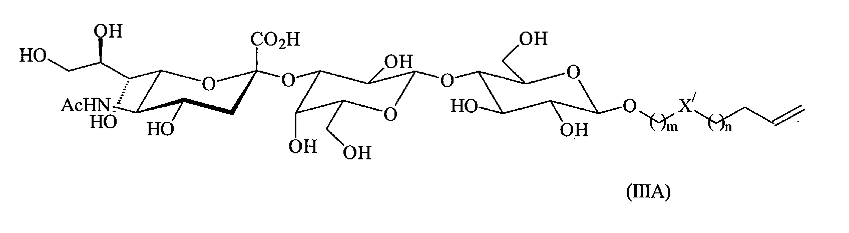

- A device obtained or obtainable by the method of claim 11 or 12.
- A device according to claim 9, wherein said silicon substrate has 2 or more, preferably 10 or more, target portions.
- A device according to claim 14, wherein the monolayer comprises receptor compounds of a first type in an area covering a first target portion, and receptor compounds of a different type in an area covering a second target portion.
- A device according to any one of claims 9 or 13 to 15, wherein the monolayer in the area covering at least one target portion comprises one or more oligosaccharide or oligopeptide derivatives.
- A device according to claim 16, wherein the monolayer in the area covering at least one target portion comprises an oligosaccharide derivative of formula (III)

- Use of a device according to any one of claims 8, 9 or 13 to 17 as a sensor.
Priority Applications (4)
| Application Number | Priority Date | Filing Date | Title |
|---|---|---|---|
| EP20030253999 EP1491884A1 (en) | 2003-06-25 | 2003-06-25 | Biosensor and method of preparation |
| TW093118383A TWI259279B (en) | 2003-06-25 | 2004-06-24 | Device manufacturing method for the production of silicon substrates having functionalized surface and device manufactured thereby |
| US10/562,212 US7507675B2 (en) | 2003-06-25 | 2004-06-24 | Device manufacturing method and device |
| PCT/EP2004/006823 WO2005001461A2 (en) | 2003-06-25 | 2004-06-24 | Biosensor and method of preparation |
Applications Claiming Priority (1)
| Application Number | Priority Date | Filing Date | Title |
|---|---|---|---|
| EP20030253999 EP1491884A1 (en) | 2003-06-25 | 2003-06-25 | Biosensor and method of preparation |
Publications (1)
| Publication Number | Publication Date |
|---|---|
| EP1491884A1 true EP1491884A1 (en) | 2004-12-29 |
Family
ID=33396020
Family Applications (1)
| Application Number | Title | Priority Date | Filing Date |
|---|---|---|---|
| EP20030253999 Withdrawn EP1491884A1 (en) | 2003-06-25 | 2003-06-25 | Biosensor and method of preparation |
Country Status (4)
| Country | Link |
|---|---|
| US (1) | US7507675B2 (en) |
| EP (1) | EP1491884A1 (en) |
| TW (1) | TWI259279B (en) |
| WO (1) | WO2005001461A2 (en) |
Cited By (2)
| Publication number | Priority date | Publication date | Assignee | Title |
|---|---|---|---|---|
| WO2010050806A1 (en) * | 2008-10-27 | 2010-05-06 | Stichting Wetsus Centre Of Excellence For Sustainable Water Technology | Capacitance electrode and sensor-system capable of sensing contaminants and method therefor |
| CN105960592A (en) * | 2013-09-18 | 2016-09-21 | 苏普拉传感器技术有限责任公司 | Molecular receptor-based chemical field-effect transistors |
Families Citing this family (16)
| Publication number | Priority date | Publication date | Assignee | Title |
|---|---|---|---|---|
| EP2183595B1 (en) * | 2007-08-01 | 2016-04-20 | Surfix BV | Protein repelling silicon and germanium surfaces |
| US9029132B2 (en) | 2009-08-06 | 2015-05-12 | International Business Machines Corporation | Sensor for biomolecules |
| US8052931B2 (en) | 2010-01-04 | 2011-11-08 | International Business Machines Corporation | Ultra low-power CMOS based bio-sensor circuit |
| US9068935B2 (en) | 2010-04-08 | 2015-06-30 | International Business Machines Corporation | Dual FET sensor for sensing biomolecules and charged ions in an electrolyte |
| US10158928B2 (en) | 2012-04-12 | 2018-12-18 | Elwha Llc | Appurtenances for reporting information regarding wound dressings |
| US9024751B2 (en) | 2012-04-12 | 2015-05-05 | Elwha Llc | Dormant to active appurtenances for reporting information regarding wound dressings |
| US10265219B2 (en) | 2012-04-12 | 2019-04-23 | Elwha Llc | Wound dressing monitoring systems including appurtenances for wound dressings |
| US9084530B2 (en) | 2012-04-12 | 2015-07-21 | Elwha Llc | Computational methods and systems for reporting information regarding appurtenances to wound dressings |
| US10130518B2 (en) | 2012-04-12 | 2018-11-20 | Elwha Llc | Appurtenances including sensors for reporting information regarding wound dressings |
| US10226212B2 (en) | 2012-04-12 | 2019-03-12 | Elwha Llc | Appurtenances to cavity wound dressings |
| EP2650938A1 (en) * | 2012-04-13 | 2013-10-16 | Acreo Swedish ICT AB | Organic Field-Effect Transistor Device |
| US9919112B2 (en) | 2014-06-30 | 2018-03-20 | Elwha Llc | Active lubrication of penetrating devices |
| US9919111B2 (en) | 2014-06-30 | 2018-03-20 | Elwha Llc | Active lubrication of penetrating devices |
| US9730724B2 (en) | 2014-10-09 | 2017-08-15 | Elwha Llc | Systems and devices for cutting tissue |
| US9730720B2 (en) | 2014-10-09 | 2017-08-15 | Elwha Llc | Systems and devices for cutting tissue |
| US9730725B2 (en) | 2014-10-09 | 2017-08-15 | Elwha Llc | Systems and devices for cutting tissue |
Citations (2)
| Publication number | Priority date | Publication date | Assignee | Title |
|---|---|---|---|---|
| WO2000026019A1 (en) * | 1998-11-02 | 2000-05-11 | Purdue Research Foundation | Functionalized porous silicon surfaces |
| US6485986B1 (en) * | 1999-11-19 | 2002-11-26 | Purdue Research Foundation | Functionalized silicon surfaces |
Family Cites Families (1)
| Publication number | Priority date | Publication date | Assignee | Title |
|---|---|---|---|---|
| EP1363122A1 (en) | 2002-05-17 | 2003-11-19 | Wageningen Universiteit | Method for producing a hybrid organic silicon field effect transistor structure |
-
2003
- 2003-06-25 EP EP20030253999 patent/EP1491884A1/en not_active Withdrawn
-
2004
- 2004-06-24 TW TW093118383A patent/TWI259279B/en not_active IP Right Cessation
- 2004-06-24 US US10/562,212 patent/US7507675B2/en not_active Expired - Fee Related
- 2004-06-24 WO PCT/EP2004/006823 patent/WO2005001461A2/en not_active Ceased
Patent Citations (2)
| Publication number | Priority date | Publication date | Assignee | Title |
|---|---|---|---|---|
| WO2000026019A1 (en) * | 1998-11-02 | 2000-05-11 | Purdue Research Foundation | Functionalized porous silicon surfaces |
| US6485986B1 (en) * | 1999-11-19 | 2002-11-26 | Purdue Research Foundation | Functionalized silicon surfaces |
Cited By (6)
| Publication number | Priority date | Publication date | Assignee | Title |
|---|---|---|---|---|
| WO2010050806A1 (en) * | 2008-10-27 | 2010-05-06 | Stichting Wetsus Centre Of Excellence For Sustainable Water Technology | Capacitance electrode and sensor-system capable of sensing contaminants and method therefor |
| EP2375245A1 (en) * | 2008-10-27 | 2011-10-12 | Smart Frequencies B.V. | Capacitance electrode and sensor-system capable of sensing contaminants and method therefor |
| CN102257382A (en) * | 2008-10-27 | 2011-11-23 | 斯马特频率有限公司 | Capacitive electrode and sensor system capable of sensing pollutants and method thereof |
| CN105960592A (en) * | 2013-09-18 | 2016-09-21 | 苏普拉传感器技术有限责任公司 | Molecular receptor-based chemical field-effect transistors |
| CN110988085A (en) * | 2013-09-18 | 2020-04-10 | 苏普拉传感器技术有限责任公司 | Molecular receptor-based chemical field-effect transistors |
| CN110988085B (en) * | 2013-09-18 | 2023-07-04 | 克莱米特有限责任公司 | Molecular receptor-based chemical field-effect transistors |
Also Published As
| Publication number | Publication date |
|---|---|
| US20070178707A1 (en) | 2007-08-02 |
| WO2005001461A3 (en) | 2005-04-21 |
| TW200519378A (en) | 2005-06-16 |
| US7507675B2 (en) | 2009-03-24 |
| TWI259279B (en) | 2006-08-01 |
| WO2005001461A2 (en) | 2005-01-06 |
Similar Documents
| Publication | Publication Date | Title |
|---|---|---|
| EP1491884A1 (en) | Biosensor and method of preparation | |
| Lin et al. | DNA attachment and hybridization at the silicon (100) surface | |
| JP4857820B2 (en) | DNA sensing method | |
| US8198071B2 (en) | Substrate for biochip, biochip, method for manufacturing substrate for biochip, and method for manufacturing biochip | |
| Onclin et al. | Molecular printboards: monolayers of β-cyclodextrins on silicon oxide surfaces | |
| US20040048241A1 (en) | Methods for attaching molecules | |
| EP2154525B1 (en) | Electrical detection and/or quantification of organophosphorous compounds | |
| EP2130045B1 (en) | A novel potentiometric cholesterol sensor for the quantitative estimation of total cholesterol in human blood serum | |
| JP5483150B2 (en) | DNA sensing method | |
| EP2017609A1 (en) | Method and device for high sensitivity and quantitative detection of chemical/biological molecules | |
| Han et al. | Detection of DNA hybridization by a field‐effect transistor with covalently attached catcher molecules | |
| JP2001520396A (en) | High surface density covalent immobilization of oligonucleotide monolayers | |
| Niwa et al. | Organosilane self-assembled monolayer-modified field effect transistors for on-chip ion and biomolecule sensing | |
| JP4049250B2 (en) | Semiconductor sensing device, manufacturing method thereof, and sensor having the device | |
| KR20080086387A (en) | Manufacturing method of substrate for microarray manufacturing | |
| Turko et al. | Langmuir-Blodgett films of immunoglobulin G for immunosensors | |
| Li et al. | Effect of Electric Fields on Silicon-Based Monolayers | |
| Geiger et al. | Chromatic Transitions in Polydiacetylene Langmuir‐Blodgett Films due to Molecular Recognition at the Film Surface Studied by Spectroscopic Methods and Surface Analysis | |
| Coffinier et al. | Surface modification of semiconducting silicon nanowires for biosensing applications | |
| WO2018013586A1 (en) | Graphene bio-electronic sensing technology | |
| JP5126811B2 (en) | Organic thin film manufacturing method and pattern forming method | |
| Sánchez-Obrero et al. | Study of the self-assembly process of an oligo (ethylene glycol)-thioacetyl substituted theophylline (THEO) on gold substrates | |
| JP2005526973A (en) | Method of manufacturing organic silicon hybrid field effect transistor structure | |
| JP4606818B2 (en) | Microchip substrate, manufacturing method thereof, microchip | |
| Jaffrezic-Renault et al. | Preparation of well-engineered thin molecular layers on semiconductor-based transducers |
Legal Events
| Date | Code | Title | Description |
|---|---|---|---|
| PUAI | Public reference made under article 153(3) epc to a published international application that has entered the european phase |
Free format text: ORIGINAL CODE: 0009012 |
|
| AK | Designated contracting states |
Kind code of ref document: A1 Designated state(s): AT BE BG CH CY CZ DE DK EE ES FI FR GB GR HU IE IT LI LU MC NL PT RO SE SI SK TR |
|
| AX | Request for extension of the european patent |
Extension state: AL LT LV MK |
|
| STAA | Information on the status of an ep patent application or granted ep patent |
Free format text: STATUS: THE APPLICATION IS DEEMED TO BE WITHDRAWN |
|
| 18D | Application deemed to be withdrawn |
Effective date: 20041026 |