EP1483354B1 - Polymerisable compositions and organic light-emitting devices containing them - Google Patents
Polymerisable compositions and organic light-emitting devices containing them Download PDFInfo
- Publication number
- EP1483354B1 EP1483354B1 EP20030743927 EP03743927A EP1483354B1 EP 1483354 B1 EP1483354 B1 EP 1483354B1 EP 20030743927 EP20030743927 EP 20030743927 EP 03743927 A EP03743927 A EP 03743927A EP 1483354 B1 EP1483354 B1 EP 1483354B1
- Authority
- EP
- European Patent Office
- Prior art keywords
- film
- formula
- composition according
- group
- transporting
- Prior art date
- Legal status (The legal status is an assumption and is not a legal conclusion. Google has not performed a legal analysis and makes no representation as to the accuracy of the status listed.)
- Expired - Lifetime
Links
- 239000000203 mixture Substances 0.000 title claims abstract description 65
- 238000000034 method Methods 0.000 claims abstract description 33
- 230000008569 process Effects 0.000 claims abstract description 16
- 230000005855 radiation Effects 0.000 claims abstract description 14
- 239000000178 monomer Substances 0.000 claims description 43
- 125000003118 aryl group Chemical group 0.000 claims description 41
- 150000003573 thiols Chemical group 0.000 claims description 39
- 239000012634 fragment Substances 0.000 claims description 37
- 239000000047 product Substances 0.000 claims description 30
- 239000007787 solid Substances 0.000 claims description 27
- 239000002019 doping agent Substances 0.000 claims description 15
- 229920000642 polymer Polymers 0.000 claims description 11
- 125000006850 spacer group Chemical group 0.000 claims description 10
- 238000006116 polymerization reaction Methods 0.000 claims description 9
- 239000000758 substrate Substances 0.000 claims description 9
- 125000002915 carbonyl group Chemical group [*:2]C([*:1])=O 0.000 claims description 8
- 238000000151 deposition Methods 0.000 claims description 8
- 239000003999 initiator Substances 0.000 claims description 7
- RTZKZFJDLAIYFH-UHFFFAOYSA-N Diethyl ether Chemical compound CCOCC RTZKZFJDLAIYFH-UHFFFAOYSA-N 0.000 claims description 6
- 150000003568 thioethers Chemical class 0.000 claims description 5
- 239000007795 chemical reaction product Substances 0.000 claims description 4
- ZUOUZKKEUPVFJK-UHFFFAOYSA-N diphenyl Chemical compound C1=CC=CC=C1C1=CC=CC=C1 ZUOUZKKEUPVFJK-UHFFFAOYSA-N 0.000 claims description 4
- 229910052727 yttrium Inorganic materials 0.000 claims description 4
- 229910052721 tungsten Inorganic materials 0.000 claims description 3
- 125000000217 alkyl group Chemical group 0.000 claims description 2
- 150000001412 amines Chemical class 0.000 claims description 2
- 239000004305 biphenyl Substances 0.000 claims description 2
- 235000010290 biphenyl Nutrition 0.000 claims description 2
- 229910052796 boron Inorganic materials 0.000 claims description 2
- KPUWHANPEXNPJT-UHFFFAOYSA-N disiloxane Chemical class [SiH3]O[SiH3] KPUWHANPEXNPJT-UHFFFAOYSA-N 0.000 claims description 2
- 125000001072 heteroaryl group Chemical group 0.000 claims description 2
- 125000005842 heteroatom Chemical group 0.000 claims description 2
- 125000004433 nitrogen atom Chemical group N* 0.000 claims 2
- 239000000463 material Substances 0.000 abstract description 57
- 125000003396 thiol group Chemical class [H]S* 0.000 abstract description 6
- 230000008021 deposition Effects 0.000 abstract 1
- 230000000379 polymerizing effect Effects 0.000 abstract 1
- YMWUJEATGCHHMB-UHFFFAOYSA-N Dichloromethane Chemical compound ClCCl YMWUJEATGCHHMB-UHFFFAOYSA-N 0.000 description 92
- 239000010410 layer Substances 0.000 description 63
- ODHXBMXNKOYIBV-UHFFFAOYSA-N triphenylamine Chemical compound C1=CC=CC=C1N(C=1C=CC=CC=1)C1=CC=CC=C1 ODHXBMXNKOYIBV-UHFFFAOYSA-N 0.000 description 34
- YXFVVABEGXRONW-UHFFFAOYSA-N Toluene Chemical compound CC1=CC=CC=C1 YXFVVABEGXRONW-UHFFFAOYSA-N 0.000 description 33
- 230000015572 biosynthetic process Effects 0.000 description 24
- VLKZOEOYAKHREP-UHFFFAOYSA-N n-Hexane Chemical compound CCCCCC VLKZOEOYAKHREP-UHFFFAOYSA-N 0.000 description 24
- IJGRMHOSHXDMSA-UHFFFAOYSA-N Atomic nitrogen Chemical compound N#N IJGRMHOSHXDMSA-UHFFFAOYSA-N 0.000 description 20
- VYPSYNLAJGMNEJ-UHFFFAOYSA-N Silicium dioxide Chemical compound O=[Si]=O VYPSYNLAJGMNEJ-UHFFFAOYSA-N 0.000 description 20
- 239000007983 Tris buffer Substances 0.000 description 20
- 238000003786 synthesis reaction Methods 0.000 description 19
- 239000011541 reaction mixture Substances 0.000 description 18
- 238000006243 chemical reaction Methods 0.000 description 16
- XLYOFNOQVPJJNP-UHFFFAOYSA-N water Substances O XLYOFNOQVPJJNP-UHFFFAOYSA-N 0.000 description 16
- LFQSCWFLJHTTHZ-UHFFFAOYSA-N Ethanol Chemical compound CCO LFQSCWFLJHTTHZ-UHFFFAOYSA-N 0.000 description 14
- HEDRZPFGACZZDS-MICDWDOJSA-N Trichloro(2H)methane Chemical compound [2H]C(Cl)(Cl)Cl HEDRZPFGACZZDS-MICDWDOJSA-N 0.000 description 12
- 239000003480 eluent Substances 0.000 description 11
- 239000000243 solution Substances 0.000 description 11
- 125000004556 carbazol-9-yl group Chemical group C1=CC=CC=2C3=CC=CC=C3N(C12)* 0.000 description 10
- 229910052757 nitrogen Inorganic materials 0.000 description 10
- 238000000059 patterning Methods 0.000 description 10
- 239000000377 silicon dioxide Substances 0.000 description 10
- 102100040428 Chitobiosyldiphosphodolichol beta-mannosyltransferase Human genes 0.000 description 9
- IAZDPXIOMUYVGZ-UHFFFAOYSA-N Dimethylsulphoxide Chemical compound CS(C)=O IAZDPXIOMUYVGZ-UHFFFAOYSA-N 0.000 description 9
- 101000891557 Homo sapiens Chitobiosyldiphosphodolichol beta-mannosyltransferase Proteins 0.000 description 9
- 229910052739 hydrogen Inorganic materials 0.000 description 9
- UEEXRMUCXBPYOV-UHFFFAOYSA-N iridium;2-phenylpyridine Chemical compound [Ir].C1=CC=CC=C1C1=CC=CC=N1.C1=CC=CC=C1C1=CC=CC=N1.C1=CC=CC=C1C1=CC=CC=N1 UEEXRMUCXBPYOV-UHFFFAOYSA-N 0.000 description 9
- 239000012044 organic layer Substances 0.000 description 9
- 239000012043 crude product Substances 0.000 description 8
- 230000008018 melting Effects 0.000 description 8
- 238000002844 melting Methods 0.000 description 8
- 239000002904 solvent Substances 0.000 description 8
- OXBLVCZKDOZZOJ-UHFFFAOYSA-N 2,3-Dihydrothiophene Chemical compound C1CC=CS1 OXBLVCZKDOZZOJ-UHFFFAOYSA-N 0.000 description 7
- CSCPPACGZOOCGX-UHFFFAOYSA-N Acetone Chemical compound CC(C)=O CSCPPACGZOOCGX-UHFFFAOYSA-N 0.000 description 7
- 238000005033 Fourier transform infrared spectroscopy Methods 0.000 description 7
- -1 aliphatic thiols Chemical class 0.000 description 7
- 238000004587 chromatography analysis Methods 0.000 description 7
- 238000004020 luminiscence type Methods 0.000 description 7
- 101000979629 Homo sapiens Nucleoside diphosphate kinase A Proteins 0.000 description 6
- CSNNHWWHGAXBCP-UHFFFAOYSA-L Magnesium sulfate Chemical compound [Mg+2].[O-][S+2]([O-])([O-])[O-] CSNNHWWHGAXBCP-UHFFFAOYSA-L 0.000 description 6
- ZMXDDKWLCZADIW-UHFFFAOYSA-N N,N-Dimethylformamide Chemical compound CN(C)C=O ZMXDDKWLCZADIW-UHFFFAOYSA-N 0.000 description 6
- 102100023252 Nucleoside diphosphate kinase A Human genes 0.000 description 6
- KWYUFKZDYYNOTN-UHFFFAOYSA-M Potassium hydroxide Chemical compound [OH-].[K+] KWYUFKZDYYNOTN-UHFFFAOYSA-M 0.000 description 6
- 239000004411 aluminium Substances 0.000 description 6
- XAGFODPZIPBFFR-UHFFFAOYSA-N aluminium Chemical compound [Al] XAGFODPZIPBFFR-UHFFFAOYSA-N 0.000 description 6
- 229910052782 aluminium Inorganic materials 0.000 description 6
- 150000001875 compounds Chemical class 0.000 description 6
- 239000011521 glass Substances 0.000 description 6
- 239000007788 liquid Substances 0.000 description 6
- 239000011159 matrix material Substances 0.000 description 6
- 239000012074 organic phase Substances 0.000 description 6
- 238000010129 solution processing Methods 0.000 description 6
- 238000003756 stirring Methods 0.000 description 6
- AWXGSYPUMWKTBR-UHFFFAOYSA-N 4-carbazol-9-yl-n,n-bis(4-carbazol-9-ylphenyl)aniline Chemical class C12=CC=CC=C2C2=CC=CC=C2N1C1=CC=C(N(C=2C=CC(=CC=2)N2C3=CC=CC=C3C3=CC=CC=C32)C=2C=CC(=CC=2)N2C3=CC=CC=C3C3=CC=CC=C32)C=C1 AWXGSYPUMWKTBR-UHFFFAOYSA-N 0.000 description 5
- 125000004122 cyclic group Chemical group 0.000 description 5
- 238000000295 emission spectrum Methods 0.000 description 5
- 239000000706 filtrate Substances 0.000 description 5
- 238000010791 quenching Methods 0.000 description 5
- 238000005406 washing Methods 0.000 description 5
- VFUDMQLBKNMONU-UHFFFAOYSA-N 9-[4-(4-carbazol-9-ylphenyl)phenyl]carbazole Chemical class C12=CC=CC=C2C2=CC=CC=C2N1C1=CC=C(C=2C=CC(=CC=2)N2C3=CC=CC=C3C3=CC=CC=C32)C=C1 VFUDMQLBKNMONU-UHFFFAOYSA-N 0.000 description 4
- UJOBWOGCFQCDNV-UHFFFAOYSA-N 9H-carbazole Chemical compound C1=CC=C2C3=CC=CC=C3NC2=C1 UJOBWOGCFQCDNV-UHFFFAOYSA-N 0.000 description 4
- HEDRZPFGACZZDS-UHFFFAOYSA-N Chloroform Chemical compound ClC(Cl)Cl HEDRZPFGACZZDS-UHFFFAOYSA-N 0.000 description 4
- VEXZGXHMUGYJMC-UHFFFAOYSA-N Hydrochloric acid Chemical compound Cl VEXZGXHMUGYJMC-UHFFFAOYSA-N 0.000 description 4
- 150000001252 acrylic acid derivatives Chemical class 0.000 description 4
- 239000012267 brine Substances 0.000 description 4
- 229920006037 cross link polymer Polymers 0.000 description 4
- 239000003921 oil Substances 0.000 description 4
- 230000000171 quenching effect Effects 0.000 description 4
- 238000010992 reflux Methods 0.000 description 4
- HPALAKNZSZLMCH-UHFFFAOYSA-M sodium;chloride;hydrate Chemical compound O.[Na+].[Cl-] HPALAKNZSZLMCH-UHFFFAOYSA-M 0.000 description 4
- 238000007738 vacuum evaporation Methods 0.000 description 4
- OZAIFHULBGXAKX-UHFFFAOYSA-N 2-(2-cyanopropan-2-yldiazenyl)-2-methylpropanenitrile Chemical compound N#CC(C)(C)N=NC(C)(C)C#N OZAIFHULBGXAKX-UHFFFAOYSA-N 0.000 description 3
- FYLKHVAQFJBJOW-UHFFFAOYSA-N 9-[4-[4-(3-formylcarbazol-9-yl)phenyl]phenyl]carbazole-3-carbaldehyde Chemical group C12=CC=CC=C2C2=CC(C=O)=CC=C2N1C1=CC=C(C=2C=CC(=CC=2)N2C3=CC=C(C=O)C=C3C3=CC=CC=C32)C=C1 FYLKHVAQFJBJOW-UHFFFAOYSA-N 0.000 description 3
- OZAIFHULBGXAKX-VAWYXSNFSA-N AIBN Substances N#CC(C)(C)\N=N\C(C)(C)C#N OZAIFHULBGXAKX-VAWYXSNFSA-N 0.000 description 3
- 230000008901 benefit Effects 0.000 description 3
- DUYAAUVXQSMXQP-UHFFFAOYSA-N ethanethioic S-acid Chemical compound CC(S)=O DUYAAUVXQSMXQP-UHFFFAOYSA-N 0.000 description 3
- 238000009472 formulation Methods 0.000 description 3
- 125000000524 functional group Chemical group 0.000 description 3
- 229910052943 magnesium sulfate Inorganic materials 0.000 description 3
- 238000004519 manufacturing process Methods 0.000 description 3
- 239000011347 resin Substances 0.000 description 3
- 229920005989 resin Polymers 0.000 description 3
- 241000894007 species Species 0.000 description 3
- 238000004528 spin coating Methods 0.000 description 3
- TVIVIEFSHFOWTE-UHFFFAOYSA-K tri(quinolin-8-yloxy)alumane Chemical compound [Al+3].C1=CN=C2C([O-])=CC=CC2=C1.C1=CN=C2C([O-])=CC=CC2=C1.C1=CN=C2C([O-])=CC=CC2=C1 TVIVIEFSHFOWTE-UHFFFAOYSA-K 0.000 description 3
- JQGGYGKXKWTXTF-UHFFFAOYSA-N 1-ethenoxy-3-prop-2-enoxy-2,2-bis(prop-2-enoxymethyl)propane Chemical compound C=CCOCC(COCC=C)(COCC=C)COC=C JQGGYGKXKWTXTF-UHFFFAOYSA-N 0.000 description 2
- 238000005160 1H NMR spectroscopy Methods 0.000 description 2
- GEQBRULPNIVQPP-UHFFFAOYSA-N 2-[3,5-bis(1-phenylbenzimidazol-2-yl)phenyl]-1-phenylbenzimidazole Chemical compound C1=CC=CC=C1N1C2=CC=CC=C2N=C1C1=CC(C=2N(C3=CC=CC=C3N=2)C=2C=CC=CC=2)=CC(C=2N(C3=CC=CC=C3N=2)C=2C=CC=CC=2)=C1 GEQBRULPNIVQPP-UHFFFAOYSA-N 0.000 description 2
- 239000005725 8-Hydroxyquinoline Substances 0.000 description 2
- WSFSSNUMVMOOMR-UHFFFAOYSA-N Formaldehyde Chemical compound O=C WSFSSNUMVMOOMR-UHFFFAOYSA-N 0.000 description 2
- DBTDEFJAFBUGPP-UHFFFAOYSA-N Methanethial Chemical compound S=C DBTDEFJAFBUGPP-UHFFFAOYSA-N 0.000 description 2
- JUJWROOIHBZHMG-UHFFFAOYSA-N Pyridine Chemical compound C1=CC=NC=C1 JUJWROOIHBZHMG-UHFFFAOYSA-N 0.000 description 2
- SMWDFEZZVXVKRB-UHFFFAOYSA-N Quinoline Chemical compound N1=CC=CC2=CC=CC=C21 SMWDFEZZVXVKRB-UHFFFAOYSA-N 0.000 description 2
- PMZURENOXWZQFD-UHFFFAOYSA-L Sodium Sulfate Chemical compound [Na+].[Na+].[O-]S([O-])(=O)=O PMZURENOXWZQFD-UHFFFAOYSA-L 0.000 description 2
- QYKIQEUNHZKYBP-UHFFFAOYSA-N Vinyl ether Chemical class C=COC=C QYKIQEUNHZKYBP-UHFFFAOYSA-N 0.000 description 2
- JOBBTVPTPXRUBP-UHFFFAOYSA-N [3-(3-sulfanylpropanoyloxy)-2,2-bis(3-sulfanylpropanoyloxymethyl)propyl] 3-sulfanylpropanoate Chemical compound SCCC(=O)OCC(COC(=O)CCS)(COC(=O)CCS)COC(=O)CCS JOBBTVPTPXRUBP-UHFFFAOYSA-N 0.000 description 2
- 230000001133 acceleration Effects 0.000 description 2
- 150000001336 alkenes Chemical class 0.000 description 2
- 150000004982 aromatic amines Chemical class 0.000 description 2
- QVGXLLKOCUKJST-UHFFFAOYSA-N atomic oxygen Chemical compound [O] QVGXLLKOCUKJST-UHFFFAOYSA-N 0.000 description 2
- ZYGHJZDHTFUPRJ-UHFFFAOYSA-N benzo-alpha-pyrone Natural products C1=CC=C2OC(=O)C=CC2=C1 ZYGHJZDHTFUPRJ-UHFFFAOYSA-N 0.000 description 2
- 125000000609 carbazolyl group Chemical group C1(=CC=CC=2C3=CC=CC=C3NC12)* 0.000 description 2
- 235000001671 coumarin Nutrition 0.000 description 2
- 150000004775 coumarins Chemical class 0.000 description 2
- 238000004132 cross linking Methods 0.000 description 2
- 230000002950 deficient Effects 0.000 description 2
- 239000003599 detergent Substances 0.000 description 2
- 238000001704 evaporation Methods 0.000 description 2
- 230000008020 evaporation Effects 0.000 description 2
- 239000007850 fluorescent dye Substances 0.000 description 2
- 239000007789 gas Substances 0.000 description 2
- 230000000977 initiatory effect Effects 0.000 description 2
- 229910052741 iridium Inorganic materials 0.000 description 2
- GKOZUEZYRPOHIO-UHFFFAOYSA-N iridium atom Chemical compound [Ir] GKOZUEZYRPOHIO-UHFFFAOYSA-N 0.000 description 2
- 229920002521 macromolecule Polymers 0.000 description 2
- 229910052751 metal Inorganic materials 0.000 description 2
- 239000002184 metal Substances 0.000 description 2
- 150000002739 metals Chemical class 0.000 description 2
- 125000002524 organometallic group Chemical group 0.000 description 2
- 239000001301 oxygen Substances 0.000 description 2
- 229910052760 oxygen Inorganic materials 0.000 description 2
- 229960003540 oxyquinoline Drugs 0.000 description 2
- YJVFFLUZDVXJQI-UHFFFAOYSA-L palladium(ii) acetate Chemical compound [Pd+2].CC([O-])=O.CC([O-])=O YJVFFLUZDVXJQI-UHFFFAOYSA-L 0.000 description 2
- WXZMFSXDPGVJKK-UHFFFAOYSA-N pentaerythritol Chemical compound OCC(CO)(CO)CO WXZMFSXDPGVJKK-UHFFFAOYSA-N 0.000 description 2
- XHXFXVLFKHQFAL-UHFFFAOYSA-N phosphoryl trichloride Chemical compound ClP(Cl)(Cl)=O XHXFXVLFKHQFAL-UHFFFAOYSA-N 0.000 description 2
- BASFCYQUMIYNBI-UHFFFAOYSA-N platinum Chemical compound [Pt] BASFCYQUMIYNBI-UHFFFAOYSA-N 0.000 description 2
- BWHMMNNQKKPAPP-UHFFFAOYSA-L potassium carbonate Chemical compound [K+].[K+].[O-]C([O-])=O BWHMMNNQKKPAPP-UHFFFAOYSA-L 0.000 description 2
- 238000007639 printing Methods 0.000 description 2
- KOUKXHPPRFNWPP-UHFFFAOYSA-N pyrazine-2,5-dicarboxylic acid;hydrate Chemical compound O.OC(=O)C1=CN=C(C(O)=O)C=N1 KOUKXHPPRFNWPP-UHFFFAOYSA-N 0.000 description 2
- MCJGNVYPOGVAJF-UHFFFAOYSA-N quinolin-8-ol Chemical compound C1=CN=C2C(O)=CC=CC2=C1 MCJGNVYPOGVAJF-UHFFFAOYSA-N 0.000 description 2
- XSCHRSMBECNVNS-UHFFFAOYSA-N quinoxaline Chemical compound N1=CC=NC2=CC=CC=C21 XSCHRSMBECNVNS-UHFFFAOYSA-N 0.000 description 2
- 150000003254 radicals Chemical class 0.000 description 2
- 238000001953 recrystallisation Methods 0.000 description 2
- MFRIHAYPQRLWNB-UHFFFAOYSA-N sodium tert-butoxide Chemical compound [Na+].CC(C)(C)[O-] MFRIHAYPQRLWNB-UHFFFAOYSA-N 0.000 description 2
- 238000002207 thermal evaporation Methods 0.000 description 2
- UMGDCJDMYOKAJW-UHFFFAOYSA-N thiourea Chemical compound NC(N)=S UMGDCJDMYOKAJW-UHFFFAOYSA-N 0.000 description 2
- 238000002525 ultrasonication Methods 0.000 description 2
- 125000002348 vinylic group Chemical group 0.000 description 2
- POILWHVDKZOXJZ-ARJAWSKDSA-M (z)-4-oxopent-2-en-2-olate Chemical compound C\C([O-])=C\C(C)=O POILWHVDKZOXJZ-ARJAWSKDSA-M 0.000 description 1
- HQJQYILBCQPYBI-UHFFFAOYSA-N 1-bromo-4-(4-bromophenyl)benzene Chemical group C1=CC(Br)=CC=C1C1=CC=C(Br)C=C1 HQJQYILBCQPYBI-UHFFFAOYSA-N 0.000 description 1
- VFMUXPQZKOKPOF-UHFFFAOYSA-N 2,3,7,8,12,13,17,18-octaethyl-21,23-dihydroporphyrin platinum Chemical compound [Pt].CCc1c(CC)c2cc3[nH]c(cc4nc(cc5[nH]c(cc1n2)c(CC)c5CC)c(CC)c4CC)c(CC)c3CC VFMUXPQZKOKPOF-UHFFFAOYSA-N 0.000 description 1
- FQJQNLKWTRGIEB-UHFFFAOYSA-N 2-(4-tert-butylphenyl)-5-[3-[5-(4-tert-butylphenyl)-1,3,4-oxadiazol-2-yl]phenyl]-1,3,4-oxadiazole Chemical compound C1=CC(C(C)(C)C)=CC=C1C1=NN=C(C=2C=C(C=CC=2)C=2OC(=NN=2)C=2C=CC(=CC=2)C(C)(C)C)O1 FQJQNLKWTRGIEB-UHFFFAOYSA-N 0.000 description 1
- ATVJXMYDOSMEPO-UHFFFAOYSA-N 3-prop-2-enoxyprop-1-ene Chemical compound C=CCOCC=C ATVJXMYDOSMEPO-UHFFFAOYSA-N 0.000 description 1
- CSDQQAQKBAQLLE-UHFFFAOYSA-N 4-(4-chlorophenyl)-4,5,6,7-tetrahydrothieno[3,2-c]pyridine Chemical compound C1=CC(Cl)=CC=C1C1C(C=CS2)=C2CCN1 CSDQQAQKBAQLLE-UHFFFAOYSA-N 0.000 description 1
- ZRXVCYGHAUGABY-UHFFFAOYSA-N 4-bromo-n,n-bis(4-bromophenyl)aniline Chemical compound C1=CC(Br)=CC=C1N(C=1C=CC(Br)=CC=1)C1=CC=C(Br)C=C1 ZRXVCYGHAUGABY-UHFFFAOYSA-N 0.000 description 1
- AOQKGYRILLEVJV-UHFFFAOYSA-N 4-naphthalen-1-yl-3,5-diphenyl-1,2,4-triazole Chemical compound C1=CC=CC=C1C(N1C=2C3=CC=CC=C3C=CC=2)=NN=C1C1=CC=CC=C1 AOQKGYRILLEVJV-UHFFFAOYSA-N 0.000 description 1
- ZOXJGFHDIHLPTG-UHFFFAOYSA-N Boron Chemical group [B] ZOXJGFHDIHLPTG-UHFFFAOYSA-N 0.000 description 1
- 241000566113 Branta sandvicensis Species 0.000 description 1
- CRUMWQYBHBFPRS-UHFFFAOYSA-N C(C)(C)(C)P.[P] Chemical compound C(C)(C)(C)P.[P] CRUMWQYBHBFPRS-UHFFFAOYSA-N 0.000 description 1
- 101000837344 Homo sapiens T-cell leukemia translocation-altered gene protein Proteins 0.000 description 1
- UFHFLCQGNIYNRP-UHFFFAOYSA-N Hydrogen Chemical compound [H][H] UFHFLCQGNIYNRP-UHFFFAOYSA-N 0.000 description 1
- 229910010084 LiAlH4 Inorganic materials 0.000 description 1
- OAICVXFJPJFONN-UHFFFAOYSA-N Phosphorus Chemical group [P] OAICVXFJPJFONN-UHFFFAOYSA-N 0.000 description 1
- CZPWVGJYEJSRLH-UHFFFAOYSA-N Pyrimidine Chemical compound C1=CN=CN=C1 CZPWVGJYEJSRLH-UHFFFAOYSA-N 0.000 description 1
- NRCMAYZCPIVABH-UHFFFAOYSA-N Quinacridone Chemical compound N1C2=CC=CC=C2C(=O)C2=C1C=C1C(=O)C3=CC=CC=C3NC1=C2 NRCMAYZCPIVABH-UHFFFAOYSA-N 0.000 description 1
- XUIMIQQOPSSXEZ-UHFFFAOYSA-N Silicon Chemical group [Si] XUIMIQQOPSSXEZ-UHFFFAOYSA-N 0.000 description 1
- 102100028692 T-cell leukemia translocation-altered gene protein Human genes 0.000 description 1
- SLGBZMMZGDRARJ-UHFFFAOYSA-N Triphenylene Natural products C1=CC=C2C3=CC=CC=C3C3=CC=CC=C3C2=C1 SLGBZMMZGDRARJ-UHFFFAOYSA-N 0.000 description 1
- XSQUKJJJFZCRTK-UHFFFAOYSA-N Urea Natural products NC(N)=O XSQUKJJJFZCRTK-UHFFFAOYSA-N 0.000 description 1
- JKVHJZAMJFGVIY-UHFFFAOYSA-N [9-[4-[4-[3-(hydroxymethyl)carbazol-9-yl]phenyl]phenyl]carbazol-3-yl]methanol Chemical group C12=CC=CC=C2C2=CC(CO)=CC=C2N1C1=CC=C(C=2C=CC(=CC=2)N2C3=CC=C(CO)C=C3C3=CC=CC=C32)C=C1 JKVHJZAMJFGVIY-UHFFFAOYSA-N 0.000 description 1
- IUHFWCGCSVTMPG-UHFFFAOYSA-N [C].[C] Chemical group [C].[C] IUHFWCGCSVTMPG-UHFFFAOYSA-N 0.000 description 1
- 238000000862 absorption spectrum Methods 0.000 description 1
- CUJRVFIICFDLGR-UHFFFAOYSA-N acetylacetonate Chemical compound CC(=O)[CH-]C(C)=O CUJRVFIICFDLGR-UHFFFAOYSA-N 0.000 description 1
- 230000004913 activation Effects 0.000 description 1
- 150000001345 alkine derivatives Chemical class 0.000 description 1
- BHELZAPQIKSEDF-UHFFFAOYSA-N allyl bromide Chemical compound BrCC=C BHELZAPQIKSEDF-UHFFFAOYSA-N 0.000 description 1
- 150000001398 aluminium Chemical class 0.000 description 1
- 150000001408 amides Chemical class 0.000 description 1
- 238000004458 analytical method Methods 0.000 description 1
- 239000008346 aqueous phase Substances 0.000 description 1
- 229910052799 carbon Inorganic materials 0.000 description 1
- CREMABGTGYGIQB-UHFFFAOYSA-N carbon carbon Chemical compound C.C CREMABGTGYGIQB-UHFFFAOYSA-N 0.000 description 1
- 239000011203 carbon fibre reinforced carbon Substances 0.000 description 1
- 238000012663 cationic photopolymerization Methods 0.000 description 1
- 230000008859 change Effects 0.000 description 1
- 239000003153 chemical reaction reagent Substances 0.000 description 1
- 239000011248 coating agent Substances 0.000 description 1
- 238000000576 coating method Methods 0.000 description 1
- 229940125773 compound 10 Drugs 0.000 description 1
- 239000013078 crystal Substances 0.000 description 1
- 239000000412 dendrimer Substances 0.000 description 1
- 229920000736 dendritic polymer Polymers 0.000 description 1
- RCJVRSBWZCNNQT-UHFFFAOYSA-N dichloridooxygen Chemical compound ClOCl RCJVRSBWZCNNQT-UHFFFAOYSA-N 0.000 description 1
- 150000002009 diols Chemical class 0.000 description 1
- 238000003618 dip coating Methods 0.000 description 1
- 238000004821 distillation Methods 0.000 description 1
- 239000012990 dithiocarbamate Substances 0.000 description 1
- 150000004659 dithiocarbamates Chemical class 0.000 description 1
- 238000005401 electroluminescence Methods 0.000 description 1
- 238000010894 electron beam technology Methods 0.000 description 1
- 238000005516 engineering process Methods 0.000 description 1
- 150000002148 esters Chemical class 0.000 description 1
- 239000002031 ethanolic fraction Substances 0.000 description 1
- 150000002170 ethers Chemical class 0.000 description 1
- 229940052303 ethers for general anesthesia Drugs 0.000 description 1
- 239000012949 free radical photoinitiator Substances 0.000 description 1
- 230000005525 hole transport Effects 0.000 description 1
- 239000001257 hydrogen Substances 0.000 description 1
- 239000012535 impurity Substances 0.000 description 1
- 238000007641 inkjet printing Methods 0.000 description 1
- 239000012212 insulator Substances 0.000 description 1
- IAPHXJRHXBQDQJ-WKMWQDDRSA-N jacobine Chemical compound C[C@@H]1O[C@]11C(=O)O[C@@H]([C@@H]23)CCN3CC=C2COC(=O)[C@](C)(O)[C@H](C)C1 IAPHXJRHXBQDQJ-WKMWQDDRSA-N 0.000 description 1
- IAPHXJRHXBQDQJ-ODLOZXJASA-N jacobine Natural products O=C1[C@@]2([C@H](C)O2)C[C@H](C)[C@](O)(C)C(=O)OCC=2[C@H]3N(CC=2)CC[C@H]3O1 IAPHXJRHXBQDQJ-ODLOZXJASA-N 0.000 description 1
- ZLVXBBHTMQJRSX-VMGNSXQWSA-N jdtic Chemical compound C1([C@]2(C)CCN(C[C@@H]2C)C[C@H](C(C)C)NC(=O)[C@@H]2NCC3=CC(O)=CC=C3C2)=CC=CC(O)=C1 ZLVXBBHTMQJRSX-VMGNSXQWSA-N 0.000 description 1
- 239000002346 layers by function Substances 0.000 description 1
- 239000012280 lithium aluminium hydride Substances 0.000 description 1
- 235000019341 magnesium sulphate Nutrition 0.000 description 1
- 230000000873 masking effect Effects 0.000 description 1
- 230000007246 mechanism Effects 0.000 description 1
- 230000005499 meniscus Effects 0.000 description 1
- LSEFCHWGJNHZNT-UHFFFAOYSA-M methyl(triphenyl)phosphanium;bromide Chemical compound [Br-].C=1C=CC=CC=1[P+](C=1C=CC=CC=1)(C)C1=CC=CC=C1 LSEFCHWGJNHZNT-UHFFFAOYSA-M 0.000 description 1
- 239000002808 molecular sieve Substances 0.000 description 1
- DCZNSJVFOQPSRV-UHFFFAOYSA-N n,n-diphenyl-4-[4-(n-phenylanilino)phenyl]aniline Chemical compound C1=CC=CC=C1N(C=1C=CC(=CC=1)C=1C=CC(=CC=1)N(C=1C=CC=CC=1)C=1C=CC=CC=1)C1=CC=CC=C1 DCZNSJVFOQPSRV-UHFFFAOYSA-N 0.000 description 1
- MUJNAWXXOJRNGK-UHFFFAOYSA-N n-[3-(6-methyl-1,2,3,4-tetrahydrocarbazol-9-yl)propyl]cyclohexanamine Chemical compound C1=2CCCCC=2C2=CC(C)=CC=C2N1CCCNC1CCCCC1 MUJNAWXXOJRNGK-UHFFFAOYSA-N 0.000 description 1
- XPRZIORDEVHURQ-UHFFFAOYSA-N n-[4-[3,5-bis(trifluoromethyl)pyrazol-1-yl]phenyl]-4-methylthiadiazole-5-carboxamide Chemical compound N1=NSC(C(=O)NC=2C=CC(=CC=2)N2C(=CC(=N2)C(F)(F)F)C(F)(F)F)=C1C XPRZIORDEVHURQ-UHFFFAOYSA-N 0.000 description 1
- 125000003518 norbornenyl group Chemical group C12(C=CC(CC1)C2)* 0.000 description 1
- 125000002868 norbornyl group Chemical group C12(CCC(CC1)C2)* 0.000 description 1
- 238000010534 nucleophilic substitution reaction Methods 0.000 description 1
- 239000013110 organic ligand Substances 0.000 description 1
- 239000003960 organic solvent Substances 0.000 description 1
- 150000004866 oxadiazoles Chemical class 0.000 description 1
- 150000002921 oxetanes Chemical class 0.000 description 1
- 150000002924 oxiranes Chemical class 0.000 description 1
- 125000000864 peroxy group Chemical group O(O*)* 0.000 description 1
- 150000002979 perylenes Chemical class 0.000 description 1
- 125000001997 phenyl group Chemical group [H]C1=C([H])C([H])=C(*)C([H])=C1[H] 0.000 description 1
- 229910052698 phosphorus Chemical group 0.000 description 1
- 239000011574 phosphorus Chemical group 0.000 description 1
- 238000001782 photodegradation Methods 0.000 description 1
- 238000000206 photolithography Methods 0.000 description 1
- 238000005424 photoluminescence Methods 0.000 description 1
- 229910052697 platinum Inorganic materials 0.000 description 1
- 238000011417 postcuring Methods 0.000 description 1
- 229910000027 potassium carbonate Inorganic materials 0.000 description 1
- LPNYRYFBWFDTMA-UHFFFAOYSA-N potassium tert-butoxide Chemical compound [K+].CC(C)(C)[O-] LPNYRYFBWFDTMA-UHFFFAOYSA-N 0.000 description 1
- 239000011253 protective coating Substances 0.000 description 1
- UMJSCPRVCHMLSP-UHFFFAOYSA-N pyridine Natural products COC1=CC=CN=C1 UMJSCPRVCHMLSP-UHFFFAOYSA-N 0.000 description 1
- 238000007761 roller coating Methods 0.000 description 1
- 229910052710 silicon Inorganic materials 0.000 description 1
- 239000010703 silicon Substances 0.000 description 1
- URGAHOPLAPQHLN-UHFFFAOYSA-N sodium aluminosilicate Chemical compound [Na+].[Al+3].[O-][Si]([O-])=O.[O-][Si]([O-])=O URGAHOPLAPQHLN-UHFFFAOYSA-N 0.000 description 1
- 239000012279 sodium borohydride Substances 0.000 description 1
- 229910000033 sodium borohydride Inorganic materials 0.000 description 1
- 159000000000 sodium salts Chemical class 0.000 description 1
- 229910052938 sodium sulfate Inorganic materials 0.000 description 1
- 235000011152 sodium sulphate Nutrition 0.000 description 1
- 230000002269 spontaneous effect Effects 0.000 description 1
- 150000001629 stilbenes Chemical class 0.000 description 1
- 235000021286 stilbenes Nutrition 0.000 description 1
- 239000000725 suspension Substances 0.000 description 1
- 125000001544 thienyl group Chemical group 0.000 description 1
- 150000007970 thio esters Chemical class 0.000 description 1
- 229910052723 transition metal Inorganic materials 0.000 description 1
- 150000003624 transition metals Chemical class 0.000 description 1
- 125000005259 triarylamine group Chemical group 0.000 description 1
- 150000003918 triazines Chemical class 0.000 description 1
- BWHDROKFUHTORW-UHFFFAOYSA-N tritert-butylphosphane Chemical compound CC(C)(C)P(C(C)(C)C)C(C)(C)C BWHDROKFUHTORW-UHFFFAOYSA-N 0.000 description 1
- 125000000391 vinyl group Chemical group [H]C([*])=C([H])[H] 0.000 description 1
Classifications
-
- H—ELECTRICITY
- H10—SEMICONDUCTOR DEVICES; ELECTRIC SOLID-STATE DEVICES NOT OTHERWISE PROVIDED FOR
- H10K—ORGANIC ELECTRIC SOLID-STATE DEVICES
- H10K85/00—Organic materials used in the body or electrodes of devices covered by this subclass
- H10K85/60—Organic compounds having low molecular weight
- H10K85/631—Amine compounds having at least two aryl rest on at least one amine-nitrogen atom, e.g. triphenylamine
- H10K85/636—Amine compounds having at least two aryl rest on at least one amine-nitrogen atom, e.g. triphenylamine comprising heteroaromatic hydrocarbons as substituents on the nitrogen atom
-
- C—CHEMISTRY; METALLURGY
- C08—ORGANIC MACROMOLECULAR COMPOUNDS; THEIR PREPARATION OR CHEMICAL WORKING-UP; COMPOSITIONS BASED THEREON
- C08G—MACROMOLECULAR COMPOUNDS OBTAINED OTHERWISE THAN BY REACTIONS ONLY INVOLVING UNSATURATED CARBON-TO-CARBON BONDS
- C08G65/00—Macromolecular compounds obtained by reactions forming an ether link in the main chain of the macromolecule
- C08G65/02—Macromolecular compounds obtained by reactions forming an ether link in the main chain of the macromolecule from cyclic ethers by opening of the heterocyclic ring
- C08G65/32—Polymers modified by chemical after-treatment
- C08G65/329—Polymers modified by chemical after-treatment with organic compounds
-
- C—CHEMISTRY; METALLURGY
- C09—DYES; PAINTS; POLISHES; NATURAL RESINS; ADHESIVES; COMPOSITIONS NOT OTHERWISE PROVIDED FOR; APPLICATIONS OF MATERIALS NOT OTHERWISE PROVIDED FOR
- C09K—MATERIALS FOR MISCELLANEOUS APPLICATIONS, NOT PROVIDED FOR ELSEWHERE
- C09K11/00—Luminescent, e.g. electroluminescent, chemiluminescent materials
- C09K11/06—Luminescent, e.g. electroluminescent, chemiluminescent materials containing organic luminescent materials
-
- H—ELECTRICITY
- H10—SEMICONDUCTOR DEVICES; ELECTRIC SOLID-STATE DEVICES NOT OTHERWISE PROVIDED FOR
- H10K—ORGANIC ELECTRIC SOLID-STATE DEVICES
- H10K85/00—Organic materials used in the body or electrodes of devices covered by this subclass
- H10K85/10—Organic polymers or oligomers
- H10K85/111—Organic polymers or oligomers comprising aromatic, heteroaromatic, or aryl chains, e.g. polyaniline, polyphenylene or polyphenylene vinylene
-
- H—ELECTRICITY
- H10—SEMICONDUCTOR DEVICES; ELECTRIC SOLID-STATE DEVICES NOT OTHERWISE PROVIDED FOR
- H10K—ORGANIC ELECTRIC SOLID-STATE DEVICES
- H10K85/00—Organic materials used in the body or electrodes of devices covered by this subclass
- H10K85/10—Organic polymers or oligomers
- H10K85/141—Organic polymers or oligomers comprising aliphatic or olefinic chains, e.g. poly N-vinylcarbazol, PVC or PTFE
-
- H—ELECTRICITY
- H10—SEMICONDUCTOR DEVICES; ELECTRIC SOLID-STATE DEVICES NOT OTHERWISE PROVIDED FOR
- H10K—ORGANIC ELECTRIC SOLID-STATE DEVICES
- H10K85/00—Organic materials used in the body or electrodes of devices covered by this subclass
- H10K85/60—Organic compounds having low molecular weight
- H10K85/649—Aromatic compounds comprising a hetero atom
- H10K85/657—Polycyclic condensed heteroaromatic hydrocarbons
-
- C—CHEMISTRY; METALLURGY
- C08—ORGANIC MACROMOLECULAR COMPOUNDS; THEIR PREPARATION OR CHEMICAL WORKING-UP; COMPOSITIONS BASED THEREON
- C08L—COMPOSITIONS OF MACROMOLECULAR COMPOUNDS
- C08L2203/00—Applications
- C08L2203/02—Applications for biomedical use
-
- C—CHEMISTRY; METALLURGY
- C09—DYES; PAINTS; POLISHES; NATURAL RESINS; ADHESIVES; COMPOSITIONS NOT OTHERWISE PROVIDED FOR; APPLICATIONS OF MATERIALS NOT OTHERWISE PROVIDED FOR
- C09K—MATERIALS FOR MISCELLANEOUS APPLICATIONS, NOT PROVIDED FOR ELSEWHERE
- C09K2211/00—Chemical nature of organic luminescent or tenebrescent compounds
- C09K2211/10—Non-macromolecular compounds
- C09K2211/1003—Carbocyclic compounds
- C09K2211/1011—Condensed systems
-
- C—CHEMISTRY; METALLURGY
- C09—DYES; PAINTS; POLISHES; NATURAL RESINS; ADHESIVES; COMPOSITIONS NOT OTHERWISE PROVIDED FOR; APPLICATIONS OF MATERIALS NOT OTHERWISE PROVIDED FOR
- C09K—MATERIALS FOR MISCELLANEOUS APPLICATIONS, NOT PROVIDED FOR ELSEWHERE
- C09K2211/00—Chemical nature of organic luminescent or tenebrescent compounds
- C09K2211/10—Non-macromolecular compounds
- C09K2211/1003—Carbocyclic compounds
- C09K2211/1014—Carbocyclic compounds bridged by heteroatoms, e.g. N, P, Si or B
-
- C—CHEMISTRY; METALLURGY
- C09—DYES; PAINTS; POLISHES; NATURAL RESINS; ADHESIVES; COMPOSITIONS NOT OTHERWISE PROVIDED FOR; APPLICATIONS OF MATERIALS NOT OTHERWISE PROVIDED FOR
- C09K—MATERIALS FOR MISCELLANEOUS APPLICATIONS, NOT PROVIDED FOR ELSEWHERE
- C09K2211/00—Chemical nature of organic luminescent or tenebrescent compounds
- C09K2211/10—Non-macromolecular compounds
- C09K2211/1018—Heterocyclic compounds
- C09K2211/1025—Heterocyclic compounds characterised by ligands
- C09K2211/1029—Heterocyclic compounds characterised by ligands containing one nitrogen atom as the heteroatom
-
- H—ELECTRICITY
- H10—SEMICONDUCTOR DEVICES; ELECTRIC SOLID-STATE DEVICES NOT OTHERWISE PROVIDED FOR
- H10K—ORGANIC ELECTRIC SOLID-STATE DEVICES
- H10K50/00—Organic light-emitting devices
- H10K50/10—OLEDs or polymer light-emitting diodes [PLED]
- H10K50/11—OLEDs or polymer light-emitting diodes [PLED] characterised by the electroluminescent [EL] layers
-
- H—ELECTRICITY
- H10—SEMICONDUCTOR DEVICES; ELECTRIC SOLID-STATE DEVICES NOT OTHERWISE PROVIDED FOR
- H10K—ORGANIC ELECTRIC SOLID-STATE DEVICES
- H10K50/00—Organic light-emitting devices
- H10K50/10—OLEDs or polymer light-emitting diodes [PLED]
- H10K50/14—Carrier transporting layers
-
- Y—GENERAL TAGGING OF NEW TECHNOLOGICAL DEVELOPMENTS; GENERAL TAGGING OF CROSS-SECTIONAL TECHNOLOGIES SPANNING OVER SEVERAL SECTIONS OF THE IPC; TECHNICAL SUBJECTS COVERED BY FORMER USPC CROSS-REFERENCE ART COLLECTIONS [XRACs] AND DIGESTS
- Y10—TECHNICAL SUBJECTS COVERED BY FORMER USPC
- Y10S—TECHNICAL SUBJECTS COVERED BY FORMER USPC CROSS-REFERENCE ART COLLECTIONS [XRACs] AND DIGESTS
- Y10S428/00—Stock material or miscellaneous articles
- Y10S428/917—Electroluminescent
-
- Y—GENERAL TAGGING OF NEW TECHNOLOGICAL DEVELOPMENTS; GENERAL TAGGING OF CROSS-SECTIONAL TECHNOLOGIES SPANNING OVER SEVERAL SECTIONS OF THE IPC; TECHNICAL SUBJECTS COVERED BY FORMER USPC CROSS-REFERENCE ART COLLECTIONS [XRACs] AND DIGESTS
- Y10—TECHNICAL SUBJECTS COVERED BY FORMER USPC
- Y10T—TECHNICAL SUBJECTS COVERED BY FORMER US CLASSIFICATION
- Y10T428/00—Stock material or miscellaneous articles
- Y10T428/31504—Composite [nonstructural laminate]
- Y10T428/31855—Of addition polymer from unsaturated monomers
- Y10T428/31909—Next to second addition polymer from unsaturated monomers
Definitions
- OLEDs Organic light emitting diodes
- an OLED or organic electroluminescent device
- a thin organic layer or stack of organic layers sandwiched between two electrodes, such that when a voltage is applied, visible light is emitted.
- At least one of the electrodes must be transparent to visible light.
- the most efficient OLED devices have multi-layer structures (fluorescent emitter: e.g. US 5,719,467 (Hewlett-Packard 1995), EP 0,921,578 (CDT 1998), US 6,048,573 (Kodak 1998), US 6,069,442 (Kodak 1997), US 5,554,450 (Kodak 1995); phosphorescent emitter: e.g. WO 00/57676 and US 6303238 ).
- Such multi-layer structures can be formed by thermal evaporation, but when solution-processing techniques are used, depositing a second layer may wash away the first layer.
- BASF US 5518824 discusses the principle of forming, an OLED using a crosslinkable charge-transporting material.
- the proposed functional groups are acrylates, vinylethers and epoxides.
- the material is deposited from solution, and then exposed to UV light, which crosslinks the material making it insoluble. Subsequent luminescent or electron transporting layers can be deposited on top of the insoluble layer.
- BASF mentions that if the UV exposure is carried out through a mask, then the exposed areas will be insoluble and the unexposed areas still soluble, and developing (washing) this film in solvent will remove the unexposed material, leaving the insoluble patterned material. However, this patterning is not demonstrated.
- BASF discuss doping the film with a fluorescent dye or using a crosslinkable fluorescent dye ( US 5922481 ) to form the light-emitting layer.
- the EL device results reported by BASF from its crosslinked devices are very poor.
- the two devices reported, which have crosslinked but un-patterned light emitting layers, give light emission only at 87 V and 91 V, respectively, both of which are entirely unacceptable operating voltages for an OLED.
- Canon EP 1146574 A2
- Bayerl et al. (Macromolecules 1999, 20, 224-228 ) used crosslinked oxetane-bisfunctionalized N, N, N', N'-tetraphenyl-benzidine as the hole transporting material in a two-layer device. However, they did not pattern the hole-transporting material. Further work on oxetanes by Meerholz et al. (WO 02/10129 ) uses cationic photopolymerization to form crosslinked layers. In one instance the emissive layer was patterned. But in many cases the photoacid generated during the polymerization would attack other components of an OLED, in particular organometallic materials, and therefore such procedures would not generally be appropriate for the formation of patterned crosslinked emissive layers in OLED devices.
- Photo-polymerisable thiol/ene systems are known for various applications such as printing plates and protective coatings. In these prior applications of thiol/ene systems the resulting polymers have been insulators. Most of the thiol/ene systems mentioned in the prior art contain non-conjugated carbonyl groups rather than aliphatic thiols, as aliphatic thiols can retain a nasty smell.
- PETMP Peneerythritol tetrakis (3-mercaptopropionate)
- thiol component e. g. US 5100929 and US 5167882 .
- EP-A-0492953 discloses a stereolithography method for building a three-dimensional article comprising the steps of patternwise curing successive layers of a bath of curable liquid resin formulation until the article has been completely built up, removing the article from the liquid resin bath and then post-curing the article, wherein the liquid resin is a thiol/nene formulation comprising a first compound having a plurality of norbornene groups thereon, a second compound having a plurality of thiol groups therein, and a free radical photoinitiator.
- US-A-6111063 discloses a photoluminescent polymer having a repeating unit in which an aromatic amine and a double bond are conjugated.
- EP-A-1146574 discloses an organic luminescent device comprising an organic layer including a polymerised film having at least two polymerisable double bonds.
- the present invention is directed to OLEDs that solve some of the problems in the prior art.
- the current invention is about a composition of a mixture of a thiol material and an ene material that can be polymerised to form a charge transporting or luminescent film.
- the current invention is about an OLED comprising a charge-transporting or emissive layer that has been formed by polymerising a thiol material and an ene material.
- the current invention is also about a process for forming such an OLED that includes depositing a layer of material comprising a thiol and an ene, from solution, exposing said layer to actinic radiation (UV light, visible light, electron beams or X-rays), through a mask, and then optionally developing said film.
- actinic radiation UV light, visible light, electron beams or X-rays
- a composition comprising a mixture of at least one monomer with the formula: A-(X) n (1) and at least one monomer with the formula: B-(Y) m (2) where monomers of formula (1) are polymerisable with monomers of formula (2), n and m are integers greater than or equal to 2, such that n and m may be the same or different, X is a group containing a terminal thiol, Y is a group containing a reactive unsaturated carbon-carbon bond, each X may be the same or different, each Y may be the same or different, and A and B are molecular fragments such that at least one of A or B is an organic charge-transporting or organic light-emitting fragment, wherein A, B, X and Y do not contain any carbonyl groups.
- a solid film comprising a radiation-induced polymerisation reaction product of a composition according to the first aspect of the invention.
- a solid film comprising a polymer with repeat unit -(A-Z-B-W)- (3) where A and B are as defined above, Z is the addition product of the thiol- containing group, X, and the group containing a reactive unsaturated carbon- carbon bond, Y, and W is the addition product of the group containing a reactive unsaturated carbon-carbon bond, Y and the thiol-containing group, X.
- an OLED device comprising, laminated in sequence, a substrate, a first electrode, a first optional charge-transporting layer, a light-emitting layer, a second optional charge-transporting layer and a counter electrode wherein at least one of the optional charge-transporting layers and/or the light-emitting layer is according to the second or third aspects of the invention.
- compositions comprising a mixture of at least one monomer with the formula: A-(X) n (1) and at least one monomer with the formula: B-(Y) m (2) where monomers of formula (1) are polymerisable with monomers of formula (2), n and m are integers greater than or equal to 2, such that n and m may be the same or different, X is a group containing a terminal thiol, Y is a group containing a reactive unsaturated carbon-carbon bond, each X may be the same or different, each Y may be the same or different, and A and B are molecular fragments such that at least one of A or B is an organic charge transporting or organic light-emitting fragment, wherein A, B, X and Y do not contain any carbonyl groups.
- reactive unsaturated carbon-carbon bond means a group that will react under the correct conditions with a thiol to form a thioether linkage.
- Reactive unsaturated carbon-carbon groups are those with carbon-carbon double or triple bonds such as alkenes, alkynes and strained ring systems. In contrast the unsaturated carbon-carbon bonds in an aromatic ring would not react with a thiol to give a thioether linkage and so are un-reactive groups.
- Reactive unsaturated carbon-carbon bonds are often located at a terminal position in the chain or branch.
- X and Y are groups capable of undergoing free-radical induced polymerisation.
- the free-radical induced polymerisation can take place in the presence of a radical initiator. It is desirable that the resulting polymer is insoluble in a solvent that can be used to wash off the un-reacted monomers. Therefore, it is preferred that a crosslinked polymer network is formed, i.e. that n + m > 4.
- the exposure to actinic radiation is preferably done in an inert atmosphere to avoid the formation of peroxy groups in the polymer. Following washing or developing of the film, the film may be dried or undergo other post-patterning treatment.
- thiol monomer there may be other components in the film in addition to the thiol monomer and the monomer containing a reactive unsaturated carbon-carbon bond.
- a radical initiator there may be a luminescent dopant, or a charge-transporting molecule in the mixture.
- X and Y are groups capable of undergoing photo-initiated free-radical induced polymerisation.
- X is a group containing a terminal thiol.
- Y is a group containing a reactive unsaturated carbon-carbon bond or part of an unsaturated strained ring system. For brevity such a group is sometimes referred to as an ene.
- X and Y are preferably connected to A and B by spacer units. Under the correct conditions X and Y react to form a thioether linkage. The reaction proceeds by a step growth mechanism, as illustrated in the reaction scheme below ( Jacobine, Radiat. Curing Polym. Sci. Technol., 1993, 3,219-68 ).
- the ene is a double bond but it could be a triple bond or an unsaturated strained ring system.
- Initiation involves the formation of thiyl radicals. Then a thiyl radical attacks the reactive double bond, Y, to give a ⁇ -thioether carbon radical, which then abstracts a hydrogen from another thiol group, creating a new thiyl radical, which can propagate the reaction.
- the polymerisation reaction produce of the thiol monomer (1) and the ene monomer (2) is a polymer with repeat unit -(A-Z-B-W)- (3) where A and B are as defined above, Z is the addition product of the thiol-containing group, X, and the reactive unsaturated carbon-carbon bond, Y, and W is the addition product of the reactive unsaturated carbon-carbon bond, Y and the thiol-containing group, X.
- both A and B should contain charge-transporting or emissive groups, i.e. be functional. If A and B have dissimilar molecular weights, however, it would be possible for the high molecular weight (i.e. oligomeric) group to be charge transporting or emissive while the low molecular weight group is neither charge transporting nor emissive. However, the resulting polymerised film should have electroluminescent or charge-transporting properties.
- the fragments A and B can have different properties depending on required function of the photopolymer layer.
- the photopolymer functions as a charge-transport layer in an OLED.
- both fragments, A and B should contain charge-transporting groups, unless one fragment has much higher molecular weight than the other in which case said fragment alone can be charge-transporting.
- the photo-polymer forms the emissive layer.
- one or both organic fragments can be a light-emitting fragment and the fragments that are not light-emitting are preferably charge transporting, so for example one of A or B is a light-emitting fragment and the other is a charge-transporting fragment.
- neither fragment A nor B is light-emitting but the photopolymer is used as a charge-transporting host matrix for an emissive dopant. If one fragment has much higher molecular weight than the other, said fragment alone can be charge transporting or emissive. It is also possible for an emissive dopant to be used with a photopolymer host that is itself emissive, i.e. where at least one of A and B is a light-emitting fragment.
- the invention also provides an OLED device comprising, laminated in sequence, a substrate, a first electrode, a first optional charge-transporting layer, a light-emitting layer, a second optional charge-transporting layer and a counter electrode wherein at least one of the optional charge-transporting layers and/or the light-emitting layer is a solid film comprising a polymerisation reaction product of a composition comprising a mixture of at least two components with the following formulae: A-(X) n B-(Y) m , where monomers of one component are polymerisable with monomers of the other component, n and m are integers greater than or equal to 2, such that n and m may be the same or different, X represents a group containing a terminal thiol and Y represents a group containing a reactive unsaturated carbon-carbon bond, and A and B are molecular fragments such that at least one of A or B is an organic charge-transporting or organic (visible) light-emitting fragment.
- the invention also provides a method for making such an OLED, whereby the charge-transporting and/or light-emitting film is made by the process of:
- the first electrode is an anode
- the first optional charge-transporting layer is a hole-transporting layer
- the second charge-transporting layer is an electron-transporting layer
- the counter electrode is a cathode.
- the first electrode is a cathode
- the first optional charge-transporting layer is an electron-transporting layer
- the second charge-transporting layer is a hole-transporting layer
- the counter electrode is an anode.
- the light emitter is phosphorescent, it is particularly beneficially that either the electron-transporting layer also functions as a hole-blocking layer, or there is an additional hole-blocking layer between the light-emitting layer and the electron-transporting layer.
- a pixellated OLED display can either be a passive-matrix or an active-matrix display.
- the first charge-transporting layer is a polymerised film according to this invention.
- the light-emitting layer is a polymerised film according to this invention.
- both the first charge-transporting layer and the light-emitting layer are polymerised films according to this invention. It would also be possible for the first charge-transporting layer, the light-emitting layer and the second charge-transporting layer to all be polymerised films according to this invention.
- the light-emitting layer in the OLED is preferably patterned, that is a suitable photo-mask is used when the film is exposed to light.
- This patterning technique allows a multi-colour OLED to be formed.
- a key advantage of the thiol-ene system is that good resolution can be achieved when it is photo-patterned.
- a film that is capable of emitting a first colour is deposited, patterned and developed to form pixels capable of emitting a first colour. At this stage, since the film of the first colour is insoluble, it allows a film of a material that is capable of emitting a second colour to be deposited without disrupting the first colour film.
- This second film is patterned and developed to form pixels capable of emitting the second colour. The process can be repeated to deposit a material capable of emitting a third colour. If present, it may be appropriate to pattern a charge-transporting layer, and this can be done using the same masking technique.
- a solution-processing technique such as spin-coating, ink-jet printing, dip-coating meniscus or roller coating, or other printing or coating technique, or thermal-transfer method is used to deposit the thiol/ene layer which is to be polymerised.
- the fragments A and B can contain charge-transporting units. Suitable hole-transporting materials contain ⁇ -electron rich moieties. Particularly suitable are triarylamines (for examples see Shirota, J. Mater. Chem., 2000, 10, 1 -25 ).
- the charge-transporting fragment A or B can be based on known hole-transporting arylamine materials such as those with the formula where Ar is an optionally substituted aromatic group, such as phenyl, or and Ar 1 , Ar 2 , Ar 3 and Ar 4 are optionally substituted aromatic or heteroaromatic groups (Shi et al (Kodak) US 5,554,450 . Van Slyke et al, US 5,061,569 .
- Ar is preferably biphenyl.
- Ar 1 , Ar 2 , Ar 3 and Ar 4 are bonded to either a thiol group, X, or a group containing a reactive unsaturated carbon-carbon bond, Y.
- Ar 1 and Ar 2 , and/or Ar 3 and Ar 4 are optionally linked to form a N containing ring, for example so that the N forms part of a carbazole unit e.g.
- Bipolar materials that can form a bipolar fragment A or B transport both holes and electrons.
- Suitable materials preferably contain at least two carbazole units ( Shirota, J. Mater. Chem., 2000, 10, 1-25 ).
- Electron-transporting materials that can form an electron-transporting fragment A or B contain ⁇ -electron deficient moieties.
- suitable ⁇ -electron deficient moieties are oxadiazoles, triazines, pyridine, pyrimidine, quinoline, and quinoxaline ( Thelakkat, Schmidt, Polym. Adv. Technol. 1998, 9, 429-42 ).
- Alq 3 Alq 3 [Aluminium tri(8-hydroxyquinoline)]
- TAZ 3-phenyl-4-(1-naphthyl)-5-phenyl-1,2,4-triazole
- OXD-7 OXD-7 (1,3-bis(N,N-t-butyl-phenyl)-1,3,4-oxadiazole).
- one of the fragments A or B may be neither charge transporting nor luminescent, provided that the other is. If such a fragment is going to be used, it is preferred that it has a relatively low molecular mass and is the basis for a multi-functional monomer.
- a suitable fragment is based on pentaerythritol.
- monomer (1) could have the formula C(CH 2 O(CH 2 ) n X) 4 where n is an integer from 1 to 6
- monomer (2) could have the formula C(CH 2 O(CH 2 ) n Y) 4 where n is an integer from 1 to 6.
- a tetra-functional non-charge transporting thiol formed from the pentaerythritol fragment can be combined with a difunctional charge transporting ene to form a cross-linked charge-transporting film.
- Light emission may be via fluorescence or phosphorescence.
- IUPAC fluorescence is defined as spontaneous emission of radiation (luminescence) from an excited molecular entity with the formation of a molecular entity of the same spin multiplicity.
- Suitable fluorescent light-emitting materials are many organic molecules and complexes of metals of group 2, 12, 13 or light d-block metals with organic ligands. According to the colour of the light emission these materials can be divided into three groups, blue, green and red emitters.
- Suitable fluorescent blue emitters are e.g. stilbenes, coumarins, anthracences (Kodak US 5,972,247 (1999 ).Toshio et al (Toyo Ink) EP 0765106 (1996 )) and perylenes (So et al (Motorola) US 5,853,905 (1997 ). Lee et al (Motorola) US 5,747,183 (1996 )). Also suitable are blue-emitting aluminium complexes (Bryan et al (Kodak) US 5,141,671 . Van Slyke et al (Kodak) US 5,150,006 )). Suitable green emitters are Alq 3 ( Chen and Tang, Macromol.
- Suitable red emitters are DCM and its derivatives ( Chen et al, US 5,908,581 ).
- the fluorescent material can be a molecular or dendritic species. For examples of suitable fluorescent dendrimers see Samuel et al. (WO 99/21935 ).
- the light-emitting material may be a dopant in the crosslinked charge-transporting matrix (comprising charge-transporting fragments A and/or B), in which case the emission spectrum of the charge-transporting matrix should overlap the absorption spectrum of the light-emitting dopant.
- the light-emitting material may be modified so that it is itself a monomer, i.e. the light emitting material is the fragment A or B of a polymerisable material.
- the dopant can be a single material or a mixture of compounds. The concentration of the dopants is chosen so as to maximise colour purity, efficiency, and lifetime.
- phosphorescence designates luminescence involving change in spin multiplicity, typically from triplet to singlet or vice versa.
- the luminescence from a quartet state to a doublet state is also phosphorescence.
- Suitable phosphorescent light-emitting materials are heavy transition metal complexes.
- organometallic complexes of iridium for example Ir(ppy) 3 ( fac tris(2-phenylpyridine)iridium), which gives green emission (see Baldo et al., Appl. Phys. Lett., 75 no.1, 1999, 4 ), or (btp 2 )Ir(acac) (bis(2-(2'-benzo[4,5- ⁇ ]thienyl) pyridinato-N,C 3' ) iridium (acetylacetonate)), which gives red emission (see Adachi et al., Appl. Phys.
- the phosphorescent material can be a molecular or dendritic species.
- the light-emitting material may be a dopant in the crosslinked charge-transporting matrix (comprising charge-transporting fragments A and/or B), in which case the charge-transporting can be bipolar, hole transporting or electron-transporting.
- the light-emitting material may be modified so that it is itself a monomer, i.e. the light-emitting material is the fragment A or B of a crosslinkable material.
- the dopant can be a single material or a mixture of compounds. The concentration of the dopants is chosen so as to maximise colour purity, efficiency, and lifetime.
- the concentration of the phosphorescent light-emitting fragment in the host material should be such that the film has a high photoluminescent and electroluminescent efficiency. If the concentration of the emissive species is too high, quenching of luminescence can occur. A concentration in the range 0.01-49 molar %, is generally appropriate.
- thiol monomers and ene monomers suitable for use with a phosphorescent dopant, are shown in figures 1 and 2, respectively.
- a di-functional monomer derivative of CBP used with a tri-functional monomer derivative of TCTA will form a crosslinked polymer.
- a crosslinked polymer would be formed if both the thiol and ene monomers were tri-functional derivatives of TCTA.
- spacer chain between the charge-transporting or light-emitting moiety and the polymerisable thiol or the reactive unsaturated carbon-carbon bond.
- a spacer improves the film forming properties of the material, allowing good quality films to be deposited from solution.
- the spacer also aids the polymerisation process.
- the spacer should not contain any carbonyl groups (including those in the form of esters, amides etc.).
- the spacer can comprise alkyl, ether, thioether, aryl, siloxane, amine or unsaturated groups, or heteroatoms such as silicon, boron or phosphorus. In fact neither A-(X) n nor B-(Y) m should contain any carbonyl groups.
- Synthetic routes to form thiol-containing materials including those starting from thiourea, thiosulfate ions, thiol esters and dithiocarbamates can be found in S. Patai, Chapter 4, The Chemistry of the Thiol Groups, John Wiley & Sons, London 1974 .
- Thiol-ene mixtures can be easily thermally-polymerized and photo-polymerised. Photo-polymerization has the advantage that good resolution patterned films can be obtained and hence photo-polymerization is preferred for OLED applications.
- the reactive unsaturated carbon-carbon bonds are preferably electron-rich or they form part of a strained ring system. In this later case, reaction of the unsaturated carbon-carbon bond with a thiol will then release the ring strain.
- the reactive unsaturated group consists preferably of a norbornyl or vinylether moiety, other useful enes consist of allylether, or unsaturated cyclic systems.
- the thiol-ene systems there are suitable initiators for activation by either UV light or visible light. For successful initiation, it is generally preferable to use a wavelength of light that is absorbed by the initiator but not strongly absorbed by the other components of the film. In this way the initiator functions well and photo-degradation of the film is minimised.
- the thiol-ene systems mentioned here do not contain any carbonyl groups therefore no quenching of luminescence is observed. Unlike previously proposed photo-polymerisable systems proposed for OLEDs the thiol-ene systems is unique in offering a combination of high-resolution patterning with minimum luminescence quenching.
- Potassium carbonate (52.0 g, 383 mmoles) was dried under high vacuum in an oil bath at 220 oC with vigorous stirring for 90 minutes.
- Carbazole (20.9 g, 125 mmoles, previously recrystallised from toluene) and tris(4-bromophenyl)amine (20.1 g, 47 mmoles) were added and placed under high vacuum for 10 minutes.
- Anhydrous toluene (175 cm 3 ) was then added and degassed under high vacuum for 10 minutes.
- Phosphorus oxychloride (11.5 ml, 19.0 g, 115 mmol) was added dropwise to a stirring mixture of N,N-dimethylformamide (4.78 ml, 4.51 g, 61.7 mmol) and 4,4',4"-Tris(carbazole-9-yl)triphenylamine (TCTA) (20) (7.26 g, 9.81 mmol) and the resulting mixture was stirred at room temperature for 5 minutes then heated to 90°C for 5 days. The reaction mixture was poured into water (800 ml) and the flask containing the product was placed in the ultrasonic bath for 2 hours to break up the material. The mixture was stirred for 2 hours then filtered.
- TCTA 4,4',4"-Tris(carbazole-9-yl)triphenylamine
- Thiolacetic acid was purified by distillation prior to use. Thiolacetic acid (5 ml) was added to trivinyl derivative (22) (1.60 g, 1.95 mmol) that had been cooled in ice. The reaction mixture was warmed to room temperature and AIBN (a few mg) was added. The resulting mixture was heated at reflux for 1 hour (until the reaction was complete by TLC using DCM as the eluent. The excess thiol acetic acid was removed under reduced pressure and the product was dissolved in a minimum volume of dichloromethane. The crude product was purified by chromatography on silica using dichloromethane as the eluent. The product was obtained as a yellow film.
- the trithioester was dissolved in THF (20 ml) then was added to a solution of potassium hydroxide (1.28 g, 320 mmol) in water (20 ml). The resulting mixture was heated at reflux for 2 hours. The reaction mixture was cooled to room temperature and was acidified to ph 6 with a dilute solution of HCl (0.1 M). The product was extracted into dichloromethane (3 x 40 ml) and the organic phase was washed with water (100 ml) and brine (50 ml), dried (MgSO 4 ) and filtered. The filtrate was evaporated to dryness to give the crude product as a white solid.
- the photopolymerized films were developed by rinsing with pure toluene, dried under a stream of dry nitrogen and transferred to the evaporator (KJLesker) for completion of the OLED by evaporation of ETUHBL and top electrode.
- TPBI deposited by vacuum evaporation formed the ETUHBL (50 nm).
- LiF (1.2 nm) and Aluminium (100-150 nm) deposited by vacuum evaporation formed the cathode.
- Figure 4 shows the PL emission spectrum of a spin-coated film of the materials, before and after exposure to UV light i.e. before and after photopolymerisation.
- the film was prepared from a solution containing 10wt% Ir(ppy) 3 and a 1:1 ratio of 4,4',4"-tris[3-(2-thio-1-ethyl)carbazol-9-yl]triphenylamine (24) and 4,4',4"-tris(3-vinylcarbazol-9-yl)triphenylamine (22)
- the photopolymerisation was carried out as described above.
- Phosphorus tert -butyl phosphine (880 mg, 4.35 mmol) in toluene (88 ml) was added under nitrogen to a deoxygenated mixture of carbazole (11.9g, 71.0 mmol), 4,4'-dibromobiphenyl (10.0 g, 32.11 mmol), sodium tert -butoxide (23.2 g, 241 mmol) and palladium acetate (324 mg, 1.34 mmol) in toluene (50 ml) and the resulting mixture was heated at reflux under nitrogen for 10 days. The reaction mixture was cooled to room temperature and then diluted with more toluene (200 ml).
- the reaction mixture was filtered to removes sodium salt and the filtrate was removed all traces of the product.
- the filtrate was concentrated to dryness to give the crude product as a pale brown solid.
- the crude product was purified first by chromatography on silica using dichloromethane as the eluent followed by recrystallisation from toluene. The material was then sublimed at 280-281 °C at 10 -6 mm Hg to give the product 4,4'-bis(carbazol-9-yl)biphenyl as an off-white solid with melting point 280-281 °C (lit. m.p. 281°C).
- Phosphosphorus oxychloride 13 ml, 21.5 g, 140 mmol was added dropwise to a stirring mixture of N,N-dimethylformamide (5.40 ml, 5.10 g, 69.7 mmol) and 4,4'-bis(carbazol-9-yl)biphenyl (7.72 g, 16.0 mmol) and the resulting mixture was stirred at room temperature for 5 minutes then heated to 90°C for 24 h. (nb reaction mixture was followed by TLC using 5% ethanol/dichloromethane as the eluent). The reaction mixture was poured into water (800 ml) and this beaker was placed in the ultrasonic bath for 2 hours to break up the material.
- DMSO was dried over calcium hydride, then distilled under vacuum and stored over molecular sieves.
- Potassium hydroxide (2.07 g, 36.9 mmol) was added to DMSO (20 ml) and was stirred under nitrogen at room temperature for 15 min.
- the diol (2.39 g, 4.39 mmol) in DMSO (20 ml) was then added, followed by allyl bromide (2 ml, 2.80 g, 21.7 mmol) and the resulting mixture was stirred at room temperature under nitrogen overnight.
- the reaction mixture was poured into water (200 ml) and the product was extracted into dichloromethane (3 x 50ml).
- OLED devices were made using different combinations of thiol and ene.
- the thiols were compounds 24 and MAT1 and the enes were compounds 10, 22, and NME1. Tables 1 and 2 show the specific combinations that were used.
- the procedure for fabricating the devices is as follows. Ir(ppy)3 (8wt%), Thiol and Ene were dissolved in pure chloroform at total concentration 5-7 mg ml -1 . The solutions were spun onto ITO coated glass substrates (previously cleaned by ultrasonication in commercial detergent and thorough rinsing with DI water). Prior to spin-coating the dry ITO coated glass was plasma-treated in an Emitech K1050X plasma unit (process gas oxygen, 100 W, 2 min).
- the photopolymerized films were developed by rinsing with pure toluene, dried under a stream of dry nitrogen and transferred to the evaporator (KJLesker) for completion of the OLED by evaporation of ETUHBL and top electrode.
- TPBI deposited by vacuum evaporation formed the ETUHBL (50 nm).
- LiF (1.2 nm) and Aluminium (100-150 nm) deposited by vacuum evaporation formed the cathode.
- Table 1 shows the device performance at a luminance of 100 cd/m 2 100 cd/m 2 Device Thiol Ene mass (mg) ratio thiol:ene:dopant EQE (cd/A) PE (lm/W) Op.
- Table 2 shows the maximum device efficiencies for each device Device Thiol Ene Max EQE (cd/A) Corr.
- Device 2 is an example of a combination of a charge transporting thiol (24) and a tetra-functional non-charge transporting ene (NME1) doped with Ir(ppy) 3 .
- Devices 3 and 4 are examples of a combination of a non-charge transporting tetra-functional thiol (MAT1) and a charge transporting ene (10) doped with Ir(ppy) 3 .
- Films containing the liquid monomer MAT1 cure quickly, and produce the most efficient devices. It was found that films containing a liquid monomer and a solid monomer tend to cure quicker than films in which both monomers are solid, so it can be advantageous to use a liquid/solid monomer combination. All of these combinations cure without the addition of a separate initiator to the formulation.
Landscapes
- Chemical & Material Sciences (AREA)
- Materials Engineering (AREA)
- Engineering & Computer Science (AREA)
- Organic Chemistry (AREA)
- Physics & Mathematics (AREA)
- Spectroscopy & Molecular Physics (AREA)
- Polymers & Plastics (AREA)
- Medicinal Chemistry (AREA)
- Chemical Kinetics & Catalysis (AREA)
- Health & Medical Sciences (AREA)
- General Chemical & Material Sciences (AREA)
- Electroluminescent Light Sources (AREA)
- Addition Polymer Or Copolymer, Post-Treatments, Or Chemical Modifications (AREA)
- Polymers With Sulfur, Phosphorus Or Metals In The Main Chain (AREA)
- Compositions Of Macromolecular Compounds (AREA)
Abstract
Description
- Organic light emitting diodes (OLEDs) are an emerging display technology. In essence an OLED (or organic electroluminescent device) comprises a thin organic layer or stack of organic layers sandwiched between two electrodes, such that when a voltage is applied, visible light is emitted. At least one of the electrodes must be transparent to visible light.
- There are two principal techniques that can be used to deposit the organic layers in an OLED: thermal evaporation and solution processing. Solution processing has the potential to be the lower cost technique due to its potentially greater throughput and ability to handle large substrate sizes. However, several manufacturing issues still have to be resolved before solution processing of OLEDs can fulfil its potential. In a multi-colour or full-colour display the emissive organic layers need to be patterned according to the pixel layout. High-resolution displays require a high-resolution pattern for the emissive layer. To date, solution-processing techniques for patterning the emissive layer are far from ideal.
- In many cases, the most efficient OLED devices have multi-layer structures (fluorescent emitter: e.g.
US 5,719,467 (Hewlett-Packard 1995),EP 0,921,578 (CDT 1998),US 6,048,573 (Kodak 1998),US 6,069,442 (Kodak 1997),US 5,554,450 (Kodak 1995); phosphorescent emitter: e.g.WO 00/57676 US 6303238 ). Such multi-layer structures can be formed by thermal evaporation, but when solution-processing techniques are used, depositing a second layer may wash away the first layer. - It has been recognised that if a photolithographic technique could be successfully applied to the patterning of the organic layers in an OLED then this would offer many benefits. Photolithographic techniques are established in other industries and can give good resolution and high throughput. However the attempts to use photolithography during the formation of the organic layers in OLEDs have all had only very limited success.
- BASF (
US 5518824 ) discusses the principle of forming, an OLED using a crosslinkable charge-transporting material. The proposed functional groups are acrylates, vinylethers and epoxides. The material is deposited from solution, and then exposed to UV light, which crosslinks the material making it insoluble. Subsequent luminescent or electron transporting layers can be deposited on top of the insoluble layer. BASF mentions that if the UV exposure is carried out through a mask, then the exposed areas will be insoluble and the unexposed areas still soluble, and developing (washing) this film in solvent will remove the unexposed material, leaving the insoluble patterned material. However, this patterning is not demonstrated. BASF discuss doping the film with a fluorescent dye or using a crosslinkable fluorescent dye (US 5922481 ) to form the light-emitting layer. The EL device results reported by BASF from its crosslinked devices are very poor. The two devices reported, which have crosslinked but un-patterned light emitting layers, give light emission only at 87 V and 91 V, respectively, both of which are entirely unacceptable operating voltages for an OLED. Canon (EP 1146574 A2 ) also demonstrate an OLED with a crosslinked emissive film, but there is still no demonstration of a patterned emissive layer. Further, Bacher et al. (Macromolecules 1999, 32, 4551-4557) demonstrated photocrosslinking of a hole-transporting (acrylate derivative of triphenylene) material. They produced a patterned photo-crosslinked hole-transport layer on to which they deposited an emissive layer (tris(8-hydroxyquinoline)aluminium: Alq3), and made a functioning OLED device. However, they had not developed a technique for photo-lithographically patterning the emissive layer, and unless the emissive layer can also be patterned, only a monochrome device can be formed. The problem with acrylates in all the prior art is that although the acrylates can give very high resolution in the patterning process, they quench luminescence. The quenching of fluorescence by carbonyl groups is well known (Becker, Theory and Interpretation of Fluorescence and Phosphorescence, Wiley Interscience, NY 1969). - Other authors suggest crosslinking materials by thermally-initiated processes. While such processes do form insoluble films allowing subsequent layers to be deposited on top, they do not allow patterning of the layer. IBM has a patent (
US 6107452 ) on thermally/photochemically-induced crosslinking of polymers for use, for example, in light-emitting devices. No patterning was demonstrated. - Bayerl et al. (Macromolecules 1999, 20, 224-228) used crosslinked oxetane-bisfunctionalized N, N, N', N'-tetraphenyl-benzidine as the hole transporting material in a two-layer device. However, they did not pattern the hole-transporting material. Further work on oxetanes by
Meerholz et al. (WO 02/10129 - Photo-polymerisable thiol/ene systems are known for various applications such as printing plates and protective coatings. In these prior applications of thiol/ene systems the resulting polymers have been insulators. Most of the thiol/ene systems mentioned in the prior art contain non-conjugated carbonyl groups rather than aliphatic thiols, as aliphatic thiols can retain a nasty smell.
- In particular PETMP (Pentaerythritol tetrakis (3-mercaptopropionate)) is commonly used as the thiol component (e. g.
US 5100929 andUS 5167882 ). -
EP-A-0492953 discloses a stereolithography method for building a three-dimensional article comprising the steps of patternwise curing successive layers of a bath of curable liquid resin formulation until the article has been completely built up, removing the article from the liquid resin bath and then post-curing the article, wherein the liquid resin is a thiol/nene formulation comprising a first compound having a plurality of norbornene groups thereon, a second compound having a plurality of thiol groups therein, and a free radical photoinitiator. -
US-A-6111063 discloses a photoluminescent polymer having a repeating unit in which an aromatic amine and a double bond are conjugated. -
EP-A-1146574 discloses an organic luminescent device comprising an organic layer including a polymerised film having at least two polymerisable double bonds. - The present invention is directed to OLEDs that solve some of the problems in the prior art.
- The current invention is about a composition of a mixture of a thiol material and an ene material that can be polymerised to form a charge transporting or luminescent film.
- The current invention is about an OLED comprising a charge-transporting or emissive layer that has been formed by polymerising a thiol material and an ene material.
- The current invention is also about a process for forming such an OLED that includes depositing a layer of material comprising a thiol and an ene, from solution, exposing said layer to actinic radiation (UV light, visible light, electron beams or X-rays), through a mask, and then optionally developing said film.
- According to a first aspect of the current invention there is provided a composition comprising a mixture of at least one monomer with the formula:
A-(X)n (1)
and at least one monomer with the formula:
B-(Y)m (2)
where monomers of formula (1) are polymerisable with monomers of formula (2), n and m are integers greater than or equal to 2, such that n and m may be the same or different, X is a group containing a terminal thiol, Y is a group containing a reactive unsaturated carbon-carbon bond, each X may be the same or different, each Y may be the same or different, and A and B are molecular fragments such that at least one of A or B is an organic charge-transporting or organic light-emitting fragment, wherein A, B, X and Y do not contain any carbonyl groups. - According to a second aspect there is a solid film comprising a radiation-induced polymerisation reaction product of a composition according to the first aspect of the invention.
- According to a third aspect of the present invention there is provided a solid film comprising a polymer with repeat unit
-(A-Z-B-W)- (3)
where A and B are as defined above, Z is the addition product of the thiol- containing group, X, and the group containing a reactive unsaturated carbon- carbon bond, Y, and W is the addition product of the group containing a reactive unsaturated carbon-carbon bond, Y and the thiol-containing group, X. - According to a fourth aspect of the invention there is provided an OLED device comprising, laminated in sequence, a substrate, a first electrode, a first optional charge-transporting layer, a light-emitting layer, a second optional charge-transporting layer and a counter electrode wherein at least one of the optional charge-transporting layers and/or the light-emitting layer is according to the second or third aspects of the invention.
- In a further aspect of the invention there is provided a process for forming a charge-transporting or emissive layer in an OLED comprising the following steps:
- i) depositing a film with a composition according to the first aspect of the invention
- ii) polymerising said composition by exposing said film to actinic radiation, or more preferably visible or UV light.
- In yet a further aspect of the invention there is provided a process for forming a charge-transporting or emissive layer in an OLED comprising the following steps:
- i) depositing a film with a composition according to the first aspect of the invention
- ii) exposing said film to actinic radiation, or more preferably visible or UV light through a mask
- iii) washing the exposed film to remove any unexposed material.
- According to the present invention there is provided a composition comprising a mixture of at least one monomer with the formula:
A-(X)n (1)
and at least one monomer with the formula:
B-(Y)m (2)
where monomers of formula (1) are polymerisable with monomers of formula (2), n and m are integers greater than or equal to 2, such that n and m may be the same or different, X is a group containing a terminal thiol, Y is a group containing a reactive unsaturated carbon-carbon bond, each X may be the same or different, each Y may be the same or different, and A and B are molecular fragments such that at least one of A or B is an organic charge transporting or organic light-emitting fragment, wherein A, B, X and Y do not contain any carbonyl groups. - The term reactive unsaturated carbon-carbon bond means a group that will react under the correct conditions with a thiol to form a thioether linkage. Reactive unsaturated carbon-carbon groups are those with carbon-carbon double or triple bonds such as alkenes, alkynes and strained ring systems. In contrast the unsaturated carbon-carbon bonds in an aromatic ring would not react with a thiol to give a thioether linkage and so are un-reactive groups. Reactive unsaturated carbon-carbon bonds are often located at a terminal position in the chain or branch.
- X and Y are groups capable of undergoing free-radical induced polymerisation. Optionally, the free-radical induced polymerisation can take place in the presence of a radical initiator. It is desirable that the resulting polymer is insoluble in a solvent that can be used to wash off the un-reacted monomers. Therefore, it is preferred that a crosslinked polymer network is formed, i.e. that n + m > 4. The exposure to actinic radiation is preferably done in an inert atmosphere to avoid the formation of peroxy groups in the polymer. Following washing or developing of the film, the film may be dried or undergo other post-patterning treatment.
- There may be other components in the film in addition to the thiol monomer and the monomer containing a reactive unsaturated carbon-carbon bond. In particular there may be a radical initiator, a luminescent dopant, or a charge-transporting molecule in the mixture.
- X and Y are groups capable of undergoing photo-initiated free-radical induced polymerisation. X is a group containing a terminal thiol. Y is a group containing a reactive unsaturated carbon-carbon bond or part of an unsaturated strained ring system. For brevity such a group is sometimes referred to as an ene. X and Y are preferably connected to A and B by spacer units. Under the correct conditions X and Y react to form a thioether linkage. The reaction proceeds by a step growth mechanism, as illustrated in the reaction scheme below (Jacobine, Radiat. Curing Polym. Sci. Technol., 1993, 3,219-68).

- Here, for illustration, the ene is a double bond but it could be a triple bond or an unsaturated strained ring system. Initiation involves the formation of thiyl radicals. Then a thiyl radical attacks the reactive double bond, Y, to give a β-thioether carbon radical, which then abstracts a hydrogen from another thiol group, creating a new thiyl radical, which can propagate the reaction. The thiol is effectively added across the reactive double bond and the chain transferred, hence the need for multi-functional monomers. If each monomer has two functional groups (n=m=2) then a linear polymer can be formed, if at least one of n or m is greater than 2 then a crosslinked polymer can be formed.
- In principle, as many X groups as Y groups should be present for complete reaction to occur, if one group is in excess then the excess will remain un-reacted. However, as is well known, in a polymerisation reaction of multi-functional monomers assuming unlimited mobility not all functional groups react (P. J. Flory, J. Am. Chem. Soc. 1947, 69, 2893), so it is not thought to be critical that the number of X and Y groups is balanced.
- The polymerisation reaction produce of the thiol monomer (1) and the ene monomer (2) is a polymer with repeat unit
-(A-Z-B-W)- (3)
where A and B are as defined above, Z is the addition product of the thiol-containing group, X, and the reactive unsaturated carbon-carbon bond, Y, and W is the addition product of the reactive unsaturated carbon-carbon bond, Y and the thiol-containing group, X. Such a polymer comprises a further aspect of the invention. - If A and B have similar molecular weights, both A and B should contain charge-transporting or emissive groups, i.e. be functional. If A and B have dissimilar molecular weights, however, it would be possible for the high molecular weight (i.e. oligomeric) group to be charge transporting or emissive while the low molecular weight group is neither charge transporting nor emissive. However, the resulting polymerised film should have electroluminescent or charge-transporting properties.
- The fragments A and B can have different properties depending on required function of the photopolymer layer. In one embodiment, the photopolymer functions as a charge-transport layer in an OLED. In this case preferably both fragments, A and B, should contain charge-transporting groups, unless one fragment has much higher molecular weight than the other in which case said fragment alone can be charge-transporting. In another embodiment the photo-polymer forms the emissive layer. In this case, one or both organic fragments can be a light-emitting fragment and the fragments that are not light-emitting are preferably charge transporting, so for example one of A or B is a light-emitting fragment and the other is a charge-transporting fragment. Alternatively neither fragment A nor B is light-emitting but the photopolymer is used as a charge-transporting host matrix for an emissive dopant. If one fragment has much higher molecular weight than the other, said fragment alone can be charge transporting or emissive. It is also possible for an emissive dopant to be used with a photopolymer host that is itself emissive, i.e. where at least one of A and B is a light-emitting fragment.
- The invention also provides an OLED device comprising, laminated in sequence, a substrate, a first electrode, a first optional charge-transporting layer, a light-emitting layer, a second optional charge-transporting layer and a counter electrode wherein at least one of the optional charge-transporting layers and/or the light-emitting layer is a solid film comprising a polymerisation reaction product of a composition comprising a mixture of at least two components with the following formulae:
A-(X)n B-(Y)m,
where monomers of one component are polymerisable with monomers of the other component, n and m are integers greater than or equal to 2, such that n and m may be the same or different, X represents a group containing a terminal thiol and Y represents a group containing a reactive unsaturated carbon-carbon bond, and A and B are molecular fragments such that at least one of A or B is an organic charge-transporting or organic (visible) light-emitting fragment. - The invention also provides a method for making such an OLED, whereby the charge-transporting and/or light-emitting film is made by the process of:
- i) depositing a film with a composition according to this invention
- ii) exposing said film to actinic radiation, or more preferably visible or UV light, optionally through a mask,
- iii) optionally washing the exposed film to remove any unexposed material to leave a pre-determined pattern.
- In a typical type of OLED the first electrode is an anode, the first optional charge-transporting layer is a hole-transporting layer, the second charge-transporting layer is an electron-transporting layer, and the counter electrode is a cathode. However in another embodiment the first electrode is a cathode, the first optional charge-transporting layer is an electron-transporting layer, the second charge-transporting layer is a hole-transporting layer, and the counter electrode is an anode. As is well known in the field there may be additional functional layers in the OLED. If the light emitter is phosphorescent, it is particularly beneficially that either the electron-transporting layer also functions as a hole-blocking layer, or there is an additional hole-blocking layer between the light-emitting layer and the electron-transporting layer. A pixellated OLED display can either be a passive-matrix or an active-matrix display. In one embodiment the first charge-transporting layer is a polymerised film according to this invention. In a preferred embodiment the light-emitting layer is a polymerised film according to this invention. In an alternative embodiment, both the first charge-transporting layer and the light-emitting layer are polymerised films according to this invention. It would also be possible for the first charge-transporting layer, the light-emitting layer and the second charge-transporting layer to all be polymerised films according to this invention.
- The light-emitting layer in the OLED is preferably patterned, that is a suitable photo-mask is used when the film is exposed to light. This patterning technique allows a multi-colour OLED to be formed. A key advantage of the thiol-ene system is that good resolution can be achieved when it is photo-patterned. A film that is capable of emitting a first colour is deposited, patterned and developed to form pixels capable of emitting a first colour. At this stage, since the film of the first colour is insoluble, it allows a film of a material that is capable of emitting a second colour to be deposited without disrupting the first colour film. This second film is patterned and developed to form pixels capable of emitting the second colour. The process can be repeated to deposit a material capable of emitting a third colour. If present, it may be appropriate to pattern a charge-transporting layer, and this can be done using the same masking technique.
- A solution-processing technique, such as spin-coating, ink-jet printing, dip-coating meniscus or roller coating, or other printing or coating technique, or thermal-transfer method is used to deposit the thiol/ene layer which is to be polymerised.
- As discussed above, the fragments A and B can contain charge-transporting units. Suitable hole-transporting materials contain π-electron rich moieties. Particularly suitable are triarylamines (for examples see Shirota, J. Mater. Chem., 2000, 10, 1 -25). The charge-transporting fragment A or B can be based on known hole-transporting arylamine materials such as those with the formula


US 5,554,450 .Van Slyke et al, US 5,061,569 . So et al (Motorola)US 5,853,905 (1997 )). Ar is preferably biphenyl. In the current invention at least two of Ar1, Ar2, Ar3 and Ar4 are bonded to either a thiol group, X, or a group containing a reactive unsaturated carbon-carbon bond, Y. Ar1 and Ar2, and/or Ar3 and Ar4 are optionally linked to form a N containing ring, for example so that the N forms part of a carbazole unit e.g.
- Bipolar materials that can form a bipolar fragment A or B transport both holes and electrons. Suitable materials preferably contain at least two carbazole units (Shirota, J. Mater. Chem., 2000, 10, 1-25).
- Electron-transporting materials that can form an electron-transporting fragment A or B contain π-electron deficient moieties. Examples of suitable π-electron deficient moieties are oxadiazoles, triazines, pyridine, pyrimidine, quinoline, and quinoxaline (Thelakkat, Schmidt, Polym. Adv. Technol. 1998, 9, 429-42). Specific examples include Alq3 [Aluminium tri(8-hydroxyquinoline)], TAZ (3-phenyl-4-(1-naphthyl)-5-phenyl-1,2,4-triazole) and OXD-7 (1,3-bis(N,N-t-butyl-phenyl)-1,3,4-oxadiazole).
- As discussed earlier, one of the fragments A or B may be neither charge transporting nor luminescent, provided that the other is. If such a fragment is going to be used, it is preferred that it has a relatively low molecular mass and is the basis for a multi-functional monomer. A suitable fragment is based on pentaerythritol. For example monomer (1) could have the formula C(CH2O(CH2)nX)4 where n is an integer from 1 to 6, or monomer (2) could have the formula C(CH2O(CH2)nY)4 where n is an integer from 1 to 6. A tetra-functional non-charge transporting thiol formed from the pentaerythritol fragment (see example 2) can be combined with a difunctional charge transporting ene to form a cross-linked charge-transporting film.
- Light emission may be via fluorescence or phosphorescence.
- According to IUPAC fluorescence is defined as spontaneous emission of radiation (luminescence) from an excited molecular entity with the formation of a molecular entity of the same spin multiplicity. Suitable fluorescent light-emitting materials are many organic molecules and complexes of metals of group 2, 12, 13 or light d-block metals with organic ligands. According to the colour of the light emission these materials can be divided into three groups, blue, green and red emitters.
- Suitable fluorescent blue emitters are e.g. stilbenes, coumarins, anthracences (Kodak
US 5,972,247 (1999 ).Toshio et al (Toyo Ink)EP 0765106 (1996 )) and perylenes (So et al (Motorola)US 5,853,905 (1997 ). Lee et al (Motorola)US 5,747,183 (1996 )). Also suitable are blue-emitting aluminium complexes (Bryan et al (Kodak)US 5,141,671 . Van Slyke et al (Kodak)US 5,150,006 )). Suitable green emitters are Alq3 (Chen and Tang, Macromol. Symp. 1997, 125, 1-48), coumarins (Chen et al (Kodak)US 6,020,078 ) and quinacridone (Shi et al (Kodak)US 5,593,788 ). Suitable red emitters are DCM and its derivatives (Chen et al, US 5,908,581 ). The fluorescent material can be a molecular or dendritic species. For examples of suitable fluorescent dendrimers seeSamuel et al. (WO 99/21935 - According to IUPAC the term phosphorescence designates luminescence involving change in spin multiplicity, typically from triplet to singlet or vice versa. The luminescence from a quartet state to a doublet state is also phosphorescence.
- Suitable phosphorescent light-emitting materials are heavy transition metal complexes. In particular organometallic complexes of iridium for example Ir(ppy)3 (fac tris(2-phenylpyridine)iridium), which gives green emission (see Baldo et al., Appl. Phys. Lett., 75 no.1, 1999, 4), or (btp2)Ir(acac) (bis(2-(2'-benzo[4,5-α]thienyl) pyridinato-N,C3') iridium (acetylacetonate)), which gives red emission (see Adachi et al., Appl. Phys. Lett., 78 no.11, 2001, 1622) are suitable. It could also be a complex of platinum, for example 2,3,7,8,12,13,17,18-octaethyl-21H,23H-porphine platinum (PtOEP) which gives red emission. The phosphorescent material can be a molecular or dendritic species. The light-emitting material may be a dopant in the crosslinked charge-transporting matrix (comprising charge-transporting fragments A and/or B), in which case the charge-transporting can be bipolar, hole transporting or electron-transporting. Alternatively, the light-emitting material may be modified so that it is itself a monomer, i.e. the light-emitting material is the fragment A or B of a crosslinkable material. The dopant can be a single material or a mixture of compounds. The concentration of the dopants is chosen so as to maximise colour purity, efficiency, and lifetime.
- The concentration of the phosphorescent light-emitting fragment in the host material should be such that the film has a high photoluminescent and electroluminescent efficiency. If the concentration of the emissive species is too high, quenching of luminescence can occur. A concentration in the range 0.01-49 molar %, is generally appropriate.
- Preferred examples of thiol monomers and ene monomers, suitable for use with a phosphorescent dopant, are shown in figures 1 and 2, respectively. A di-functional monomer derivative of CBP used with a tri-functional monomer derivative of TCTA will form a crosslinked polymer. Alternatively a crosslinked polymer would be formed if both the thiol and ene monomers were tri-functional derivatives of TCTA.
- There is typically a spacer chain between the charge-transporting or light-emitting moiety and the polymerisable thiol or the reactive unsaturated carbon-carbon bond. Such a spacer improves the film forming properties of the material, allowing good quality films to be deposited from solution. The spacer also aids the polymerisation process. The spacer should not contain any carbonyl groups (including those in the form of esters, amides etc.). The spacer can comprise alkyl, ether, thioether, aryl, siloxane, amine or unsaturated groups, or heteroatoms such as silicon, boron or phosphorus. In fact neither A-(X)n nor B-(Y)m should contain any carbonyl groups.
- Synthetic routes to form thiol-containing materials including those starting from thiourea, thiosulfate ions, thiol esters and dithiocarbamates can be found in S. Patai, Chapter 4, The Chemistry of the Thiol Groups, John Wiley & Sons, London 1974.
- A synthetic route to alkene materials that have an ether linkage between the reactive unsaturated carbon-carbon bond and the rest of the molecule, is via a nucleophilic substitution in the presence of base as shown in figure 2 (the step from compound 10c to compound 10). Synthesis of ethers, Houben-Weyl, Methoden der organische Chemie, V1/3, Georg Thieme Verlag, Stuttgart 1965.
- Thiol-ene mixtures can be easily thermally-polymerized and photo-polymerised. Photo-polymerization has the advantage that good resolution patterned films can be obtained and hence photo-polymerization is preferred for OLED applications. The reactive unsaturated carbon-carbon bonds are preferably electron-rich or they form part of a strained ring system. In this later case, reaction of the unsaturated carbon-carbon bond with a thiol will then release the ring strain. The reactive unsaturated group consists preferably of a norbornyl or vinylether moiety, other useful enes consist of allylether, or unsaturated cyclic systems. For the thiol-ene systems there are suitable initiators for activation by either UV light or visible light. For successful initiation, it is generally preferable to use a wavelength of light that is absorbed by the initiator but not strongly absorbed by the other components of the film. In this way the initiator functions well and photo-degradation of the film is minimised.
- The thiol-ene systems mentioned here do not contain any carbonyl groups therefore no quenching of luminescence is observed. Unlike previously proposed photo-polymerisable systems proposed for OLEDs the thiol-ene systems is unique in offering a combination of high-resolution patterning with minimum luminescence quenching.
- Figure 1 shows examples of charge-transporting thiols.
- Figure 2 shows examples of charge-transporting enes.
- Figure 3 shows the electroluminescence emission spectrum of the device in example 1.
- Figure 4 shows the photoluminescence emission spectrum from a film of a thiol and an ene doped with Ir(ppy)3 before and after exposure to UV (example 1).
- The outline for the synthesis of the materials 22 and 24 is given in the following scheme.

- Potassium carbonate (52.0 g, 383 mmoles) was dried under high vacuum in an oil bath at 220 ºC with vigorous stirring for 90 minutes. Carbazole (20.9 g, 125 mmoles, previously recrystallised from toluene) and tris(4-bromophenyl)amine (20.1 g, 47 mmoles) were added and placed under high vacuum for 10 minutes. Anhydrous toluene (175 cm3) was then added and degassed under high vacuum for 10 minutes. Palladium acetate (280 mg, 1.25 mmoles) and tris-tert-butylphosphine (750 mg, 3.71 mmol) were then added and the reaction mixture was degassed under high vacuum for 10 minutes and then refluxed under nitrogen for 18 hours before being allowed to cool. As TLC analysis showed some unreacted material, anhydrous toluene (100 cm3) was added and the reaction mixture was refluxed for a further 4 hours and then allowed to cool. The reaction mixture was diluted with hexane (500 ml) and the reaction mixture was stirred at room temperature for a further 1 hour and the reaction mixture was filtered. The residue was washed with hexane (3 x 200 ml), water (5 x 200 ml) and hexane (3 x 200 ml). The residue was recrystallised from toluene twice to give white crystals 4,4',4"-Tris(carbazole-9-yl)triphenylamine (20) (25.8 g, 74%) with a melting point 298-299 °C.
- Phosphorus oxychloride (11.5 ml, 19.0 g, 115 mmol) was added dropwise to a stirring mixture of N,N-dimethylformamide (4.78 ml, 4.51 g, 61.7 mmol) and 4,4',4"-Tris(carbazole-9-yl)triphenylamine (TCTA) (20) (7.26 g, 9.81 mmol) and the resulting mixture was stirred at room temperature for 5 minutes then heated to 90°C for 5 days. The reaction mixture was poured into water (800 ml) and the flask containing the product was placed in the ultrasonic bath for 2 hours to break up the material. The mixture was stirred for 2 hours then filtered. The residue was washed with water (500 ml) followed by hexane (500 ml) then dried at the pump for 2 hours. The crude product, a brown solid, was heated at reflux with acetone (3 x 400 ml), cooled to room temperature and filtered. The product 4,4',4"-Tris(3-formylcarbazole-9-yl)triphenylamine (21) (6.09 g, 75%) was obtained as a pale brown solid with melting point 225-227°C (dec).
- Found: C, ; H, ; N, . Calculated for C57H36N4O3: C, 82.99: H, 4.40; N, 6.79. 1H n.m.r.: (300 MHz, CDCl3): δ (ppm) 7.36-7.57, m, 24 H, aromatic H; 9.97, d, 3H, J 9.10 Hz, aromatic H; 8.21, d, 3H, J 6.75 Hz, aromatic H; 8.66, s, 3H, aromatic H; 10.10, s, 3H, CHO. λmax(CH2Cl2): 233 nm (ε 82 144/ Lmol-1cm-1), 291 (74 701), 332 (56 562).
- Band gap: 3.31 eV. FTIR (solid): 3048, 2716, 1685, 1593, 1505, 1311, 1232, 1185, 808, 766, 741, 728 cm-1.
- Dry THF (20 ml) was added under nitrogen to a deoxygenated mixture of methyltriphenyl phosphonium bromide (10.5 g, 29.3 mmol) and potassium tert-butoxide (3.28 g, 29.2 mmol) and the resulting mixture was stirred at room temperature for 15 minutes. The trialdehyde 21 (5.37 g, 6.51 mmol) was added under nitrogen and the reaction mixture was stirred at room temperature for a further 2 hours. When the reaction was complete (TLC on silica using dichloromethane as the eluent) the solvent was removed under reduced pressure and then suspended in dichloromethane. The crude reaction in dichloromethane was filtered through a silica plug using 50% dichloromethane/hexane as the eluent. Recrystallisation of the product 22 was attempted using various solvents without success and the product was purified further by chromatography on silica using 50% dichloromethane/hexane as the eluent. The product 4,4',4"-tris(3-vinylcarbazol-9-yl)triphenylamine (22) (4.11 g, 77%) was obtained as a pale yellow solid with melting point 226-228°C (gel). Found: C, 87.70; H, 4.93; N, 6.47. Calculated for C60H42N4: C, 87.99;H, 5.17; N, 6.84. 1H n.m.r. (CDCl3): δ (ppm) 5,22, dd, 3 H, vinylic H, J cis10.83, J gem, 0.88 Hz: 5.79, dd, 3H, J trans17.56, J gem, 0.88 Hz; 6.92, dd, 3H, vinylic H, J trans17.56, J cis10.83 Hz; 7.30, td, 3H, aromatic H, J 7.90, J 1.17 Hz; 7.41-7.58, m, 24 H, aromatic H; 8.12-8.17, m, 6H, aromatic H. λmax(CH2Cl2):248 nm (ε 119 504/ Lmol-1cm-1), 284 (102668), 328 (66573). Band gap: 3.40 eV. FT-IR (solid): 3043, 1625, 1599, 1505, 1457, 1311, 1227, 885, 808, 745 cm-1. PL (solution): 393 nm. CIE co-ordinates (x = 0.165, y = 0.044).
- Thiolacetic acid was purified by distillation prior to use. Thiolacetic acid (5 ml) was added to trivinyl derivative (22) (1.60 g, 1.95 mmol) that had been cooled in ice. The reaction mixture was warmed to room temperature and AIBN (a few mg) was added. The resulting mixture was heated at reflux for 1 hour (until the reaction was complete by TLC using DCM as the eluent. The excess thiol acetic acid was removed under reduced pressure and the product was dissolved in a minimum volume of dichloromethane. The crude product was purified by chromatography on silica using dichloromethane as the eluent. The product was obtained as a yellow film. Attempts were made to recrystallise the product without success. The product was purified by chromatography once more using the above-mentioned conditions. The product 4,4',4"-tris[3-(2-acetylthio-1-ethyl)carbazol-9-yl]triphenylamine (23) was obtained as a yellow solid (1.27 g, 62%) with melting point 128-130 °C. Found: C, 71.67; H, 4.79; N, 4.81. Calculated for C66H54N4O3S3: C, 75.69;H, 5.20; N, 5.35. Calculated for C66H54N4O3S3 (1 mol DCM): C, 71.07;H, 4.98; N, 4.95. 1H n.m.r. (CDCl3): δ (ppm) 2.36, s, 9H, CH3; 3.08, t, 6H, CH2S, J 8.25 Hz; 3.23, t, 6H, CH2, J 8.25 Hz; 7.25-7.33, m, 3H, aromatic H; 7.39-7.59, m, 21 H, aromatic H; 7.98, d, 3H, aromatic H, Jmeta 1.10 Hz; 8.13, d, 3H, aromatic H, Jortho 7.07 Hz. λmax(CH2Cl2): 240 nm (ε 109 958 / Lmol-1cm-1), 297 (52 652), 328 (43 308). Band gap: 3.45 eV. FT-IR (solid): 3043, 2924, 1684, 1601, 1505, 1484, 1456, 1311, 1271, 1230, 1128, 1104, 944, 745 cm-1.
- The trithioester was dissolved in THF (20 ml) then was added to a solution of potassium hydroxide (1.28 g, 320 mmol) in water (20 ml). The resulting mixture was heated at reflux for 2 hours. The reaction mixture was cooled to room temperature and was acidified to ph 6 with a dilute solution of HCl (0.1 M). The product was extracted into dichloromethane (3 x 40 ml) and the organic phase was washed with water (100 ml) and brine (50 ml), dried (MgSO4) and filtered. The filtrate was evaporated to dryness to give the crude product as a white solid. The crude product was purified by chromatography on silica using dichloromethane as the eluent. The product of 4,4',4"-tris[3-(2-thio-1-ethyl)carbazol-9-yl]triphenylamine (24) obtained was a white solid (528 mg, 53%) with melting point 185-188°C. Found: C, 76.72; H, 5.37; N, 5.96. Calculated for C60H48N4S3: C, 78.22;H, 5.25; N, 6.08. Calculated for C60H48N4S3 (1 mol H2O): C, 76.72;H, 5.37; N, 5.96). 1H n.m.r. (CDCl3, 300 MHz): δ (ppm) 1.45, s, 3H, SH J 7.70 Hz; 2.91, q, 6H, CH2S, J 7.70 Hz; 3.16, t, 6H, CH2, J 7.42 Hz; 7.22-7.34, m, 3H, aromatic H; 7.36-7.60, m, 21 H, aromatic H; 7.97, d, 3H, aromatic H, Jmeta 1.10 Hz; 8.13, d, 3H, aromatic H, Jortho 7.07 Hz. λmax(CH2Cl2): 245 nm (ε 100 508/ Lmol-1cm-1), 298 (57 145), 330 (48 854). Band gap: 3.44eV. FT-IR (solid): 3043, 2963, 2926, 2556, 1601, 1505, 1484, 1456, 1310, 1262, 1229, 1103, 1064, 1014, 802, 769, 742, 726 cm-1.
- Ir(ppy)3 (8wt%) (3.4 mg), 4,4',4"-tris[3-(2-thio-1-ethyl)carbazol-9-yl]triphenylamine (24) (19.3 mg) and 4,4',4"-tris(3-vinylcarbazol-9-yl)triphenylamine (22) (19.3 mg) were dissolved in pure chloroform at total concentration 7 mg ml-1. The solutions were spun onto ITO coated glass substrates (previously cleaned by ultrasonication in commercial detergent and thorough rinsing with DI water). Prior to spin-coating the dry ITO coated glass was plasma-treated in an Emitech K1050X plasma unit (process gas oxygen, 100 W, 2 min). Solutions were spun onto the ITO substrates at 2000 rpm with acceleration 500 rs-1 for a total of 30 s giving an emitting organic layer of thickness ca 50 nm. Films were then photopolymerized under an inert atmosphere (N2) using a Hanovir UVA 250W UV source. The films were irradiated for 6 minutes through a 5" x 5" glass photo mask (cut-off 360 nm) giving a rectangular exposed area 15 x 20 mm. Overlap of this area with ITO anode and deposited aluminium cathode defines active areas consisting of 6 pixels measuring 4 x 5 mm. The photopolymerized films were developed by rinsing with pure toluene, dried under a stream of dry nitrogen and transferred to the evaporator (KJLesker) for completion of the OLED by evaporation of ETUHBL and top electrode. TPBI deposited by vacuum evaporation formed the ETUHBL (50 nm). LiF (1.2 nm) and Aluminium (100-150 nm) deposited by vacuum evaporation formed the cathode.
-
- 0.9 cd/A (@ 103.5 cd/m2), 0.28 lm/W (@ 10.2 V), turn on voltage (ToV) 6.0 V
- Max EQE 1.0 cd/A (@ 40 cd/m2, 0.36 lm/W, 8.6 V)
- Max PE 0.42 lm/W (@ 7.5 cd/m2, 0.94 cd/A, 7.1 V)
- CIE coords. x = 0.34 y = 0.59
- The EL emission spectrum is shown in Figure 3.
- Figure 4 shows the PL emission spectrum of a spin-coated film of the materials, before and after exposure to UV light i.e. before and after photopolymerisation. The film was prepared from a solution containing 10wt% Ir(ppy)3 and a 1:1 ratio of 4,4',4"-tris[3-(2-thio-1-ethyl)carbazol-9-yl]triphenylamine (24) and 4,4',4"-tris(3-vinylcarbazol-9-yl)triphenylamine (22) The photopolymerisation was carried out as described above.
-
- Procedure carried out as directed in literature: -
Nouguier R, Mchich M, j.Org.Chem.1985,50, (3296-3298) - This is a two-step synthesis starting from the material NME1.
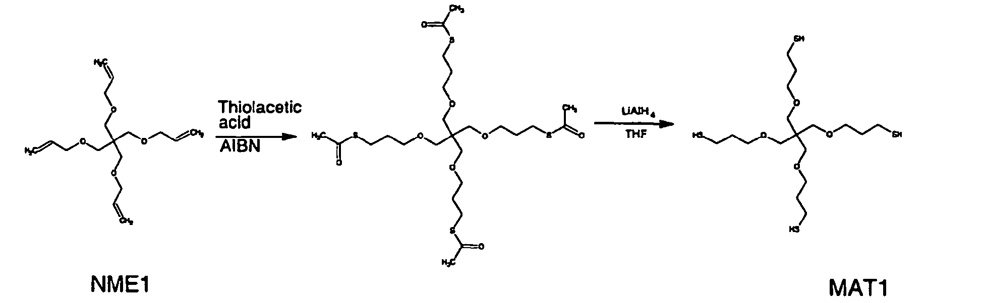
- 2.0g (6.74mmol) of tetraallylpentaerythritol was added to a 10ml round bottomed flask fitted with a stirrer. The reagent was cooled on an ice-bath where 4.11g (53.98 mmol) of freshly distilled thioacetic acid was added in 1ml portions. After the addition was complete 5mg of AIBN was added and the reaction mixture stirred for 15mins. When the AIBN had dissolved the reaction mixture was heated at 60°C for 12 hours, the reaction being followed by T.L.C. The product of the reaction had an Rf of 0.05 in dichloromethane (DCM) on silica and an Rf of 0.9 in ethanol. The excess thioacetic acid was removed from the reaction mixture under vacuum and the residue applied to a short silica column in the minimum volume of DCM. The column was eluted with 500mls of DCM followed by 500mls of ethanol. The ethanol fraction was collected and the solvent removed. 2.9g of tetrathioacetylpropylpentaerythritol was isolated as a pale yellow oil.
Yield - 71.5%
1H NMR (CDCl3) ppm: 3.41 (triplet, 8H) 3.34 (singlet, 8H) 2.92 (triplet, 8H) 2.32 (singlet, 12H) 1.80 (quintet, 8H)
I.R (cm-1): 2866.28, 1686.37, 1353.64, 1098.61, 952.97 - 1.8g (2.99mmol) of tetrathioacetylpropylpentaerythritol was added to 10m of anhydrous THF in a 100ml round bottomed flask and the mixture was degassed with stirring. The reaction vessel was purged with nitrogen and 12.3mls of 1.00M LiAlH4 in THF was added dropwise. The reaction was allowed to stir at room temperature for 18 hours, the reaction being monitored by T.L.C. (DCM as solvent) When the reaction was complete the mixture was acidified to pH 3 with 0.1 M HCl and 50mls of DCM added. The organic phase was collected, the aqueous phase extracted with 2 x 50mls of DCM. The organic phases were combined and extracted with 4 x 100ml brine and 2 x 50ml of water. The organic phase was dried over sodium sulphate, filtered and the solvent removed. The product was isolated as a pale yellow oil with a mass of 0.92g.
Yield - 71.2%.
The product was distilled on Kugelrohr apparatus to yield a mobile colourless oil, B.P 230°C @ 10-4 mbar.
1H NMR (CDCl3) ppm: 3.47 (triplet, 8H) 3.34 (singlet, 8H) 2.60 (quartet, 8H) 1.84 (quintet, 8H) 1.38 (triplet, 4H)
I.R (cm-1): 2864.30, 1368.40, 1100.51 - Phosphorus tert-butyl phosphine (880 mg, 4.35 mmol) in toluene (88 ml) was added under nitrogen to a deoxygenated mixture of carbazole (11.9g, 71.0 mmol), 4,4'-dibromobiphenyl (10.0 g, 32.11 mmol), sodium tert-butoxide (23.2 g, 241 mmol) and palladium acetate (324 mg, 1.34 mmol) in toluene (50 ml) and the resulting mixture was heated at reflux under nitrogen for 10 days. The reaction mixture was cooled to room temperature and then diluted with more toluene (200 ml). The reaction mixture was filtered to removes sodium salt and the filtrate was removed all traces of the product. The filtrate was concentrated to dryness to give the crude product as a pale brown solid. The crude product was purified first by chromatography on silica using dichloromethane as the eluent followed by recrystallisation from toluene. The material was then sublimed at 280-281 °C at 10-6 mm Hg to give the product 4,4'-bis(carbazol-9-yl)biphenyl as an off-white solid with melting point 280-281 °C (lit. m.p. 281°C).
- Phosphosphorus oxychloride (13 ml, 21.5 g, 140 mmol) was added dropwise to a stirring mixture of N,N-dimethylformamide (5.40 ml, 5.10 g, 69.7 mmol) and 4,4'-bis(carbazol-9-yl)biphenyl (7.72 g, 16.0 mmol) and the resulting mixture was stirred at room temperature for 5 minutes then heated to 90°C for 24 h. (nb reaction mixture was followed by TLC using 5% ethanol/dichloromethane as the eluent). The reaction mixture was poured into water (800 ml) and this beaker was placed in the ultrasonic bath for 2 hours to break up the material. The mixture was stirred for a further 2 hours then filtered. The residue was washed with water and then hexane and dried at the pump for 2 hours. The crude product, a brown solid, was heated with acetone (3 x 400 ml) and filtered. The product was insoluble in most organic solvent. The impurities were removed by washing with acetone. The product, 4,4'-bis(3-formylcarbazol-9-yl)biphenyl, (7.92 g, 87%) was obtained with melting point 295°C (dec.). Found: C, 81.74; H, 4.71; and N, 4.45. C38H28N2O2.(CH3)2CO requires C, 82.25; H, 5.05; N, 4.68 %). 1H n.m.r. (300 MHz, MeeSO): δ 10.09 (2 H, s, CHO); 8.88 (2 H, d, J 0.88 Hz, aromatic H); 8.41 (2 H, d, J 7.61 Hz, aromatic H); 8.41 (4 H, d, J 8.49 Hz, aromatic H); 8.00 (2 H, dd, J 8.49, 1.46 Hz, aromatic H); 7.83 (4 H, d, J 8.49 Hz, aromatic H); 7.38-7.61 (8 H, m, aromatic H). λmax(CH2Cl2): 215 nm (ε / Lmol-1cm-1 9163), 241 (68 488), 272 (65 928), 294 (67 194) 328 (42 620). FT-IR (solid): 3045, 2825, 2730, 1682, 1623, 1591, 1505, 1456, 1438, 1365, 1319, 1275, 1230, 1180, 802, 745 cm-1.
- Sodium borohydride (2.40 g, 63.4 mmol)) was added to the 4,4'-bis(3-formyl-carbazol-9-yl)biphenyl (3.42 g, 6.33 mmol) in THF (1.2 L) and the resulting suspension was stirred at room temperature for 24 h. (The reaction was followed by TLC using 5% ethanol /dichloromethane as the eluent). Once the reaction was complete, the mixture was slowly poured into water (400 ml) and the mixture was left to stir at room temperature for a further 30 min. The reaction mixture was acidified to pH 1 with hydrochloric acid (5M). The product was extracted with dichloromethane (3 x 300 ml). The combined organic phase was washed with water (400 ml) and brine (400 ml), dried (MgSO4), filtered and the filtrate evaporated to dryness. The crude product, was purified by chromatography on silica using 50% THF/toluene as the eluent. The product was recrystallised from ethanol to give 4,4'-bis(3-(hydroxymethyl)carbazol-9-yl) as a pale yellow solid (3.22 g, 94 %) with m.p. 268°C (dec.). Found: C, 82.51; H, 4.64; and N, 4.86. C38H28N2O2.EtOH requires C, 81.33; H, 5.80; N, 4.74 %). 1H n.m.r.(300 MHz, MeeSO): δ 8.23 (2 H, d, J 7.61 Hz, aromatic H); 8.18 (2 H, s, aromatic H); 8.06 (4 H, d, J 8,19 Hz, aromatic H); 7.75 (4 H, J 8,19 Hz, aromatic H); 7.38-7.50 (8 H, m, aromatic H), 7.29 (2 H, m, aromatic H); 5.25 (2H, t, J 5.58 Hz, OH); 4.68 (4H, d, J 5.56 Hz, CH2). λmax(CH2Cl2): 216 nm (ε / Lmol-1cm-1 177 455), 240 (57 873), 271 (56 595), 294 (55 330) 329 (37 758). FTIR (solid): 3343, 1604, 1500, 1485, 1455, 1362, 1330, 1230, 803, 745 cm-1.
- DMSO was dried over calcium hydride, then distilled under vacuum and stored over molecular sieves.
Potassium hydroxide (2.07 g, 36.9 mmol) was added to DMSO (20 ml) and was stirred under nitrogen at room temperature for 15 min. The diol (2.39 g, 4.39 mmol) in DMSO (20 ml) was then added, followed by allyl bromide (2 ml, 2.80 g, 21.7 mmol) and the resulting mixture was stirred at room temperature under nitrogen overnight. The reaction mixture was poured into water (200 ml) and the product was extracted into dichloromethane (3 x 50ml). The organic phases were combined and were washed with water (5 x 150 ml), brine (200 ml) and dried over magnesium sulfate. The mixture was filtered and the filtrate was evaporated to dryness. The material was purified by chromatography on silica using dichloromethane as the eluent. The relevant fractions were combined and the solvent removed under reduced pressure. The product was triturated from dichloromethane and hexane to give the product as a pale yellow solid with melting point 118-120°C. (Found: C, 82.51; H, 4.64; and N, 4.86. C38H28N2O2.EtOH requires C, 81.33; H, 5.80; N, 4.74 %). 1H n.m.r. (300 MHz, Me2SO): δ 8.13-8.20 (4 H, m, aromatic H); 7.87-7.93 (4 H, m, aromatic H); 7.65-7.72 (4 H, m, aromatic H); 7.40-7.65 (8 H, aromatic H); 7.27-7.35 (2 H, m, aromatic H); 5.93-6.09, (2H, m, CH=CH), 5.30-5.39 (2H, m, CH=CH); 5.20-5.29 (2H, m, CH=CH); 4.74 (4H, s, CH2); (8H, m, CH 2-CH=CH2). λmax(CH2Cl2): 241 nm (ε / Lmol-1cm-1 88 506), 296 (40 331), 319 (29657). FT-IR (solid): 3047, 2852, 1604, 1500, 1455, 1359, 1331, 1230, 1074, 915, 807, 759 cm-1. - OLED devices were made using different combinations of thiol and ene. In the following examples the thiols were compounds 24 and MAT1 and the enes were compounds 10, 22, and NME1. Tables 1 and 2 show the specific combinations that were used. The procedure for fabricating the devices is as follows.
Ir(ppy)3 (8wt%), Thiol and Ene were dissolved in pure chloroform at total concentration 5-7 mg ml-1. The solutions were spun onto ITO coated glass substrates (previously cleaned by ultrasonication in commercial detergent and thorough rinsing with DI water). Prior to spin-coating the dry ITO coated glass was plasma-treated in an Emitech K1050X plasma unit (process gas oxygen, 100 W, 2 min). Solutions were spun onto the ITO substrates at 2000 rpm with acceleration 500 rs-1 for a total of 30 s giving an emitting organic layer of thickness ca 50 nm. Films were then photopolymerized under an inert atmosphere (N2) using a Hanovir UVA 250W UV source. The films were irradiated for 6-8 minutes through a 5" x 5" glass photo mask (cut-off 360 nm) giving a rectangular exposed area 15 x 20 mm. Overlap of this area with ITO anode and deposited aluminium cathode defines active areas consisting of 6 pixels measuring 4 x 5 mm. The photopolymerized films were developed by rinsing with pure toluene, dried under a stream of dry nitrogen and transferred to the evaporator (KJLesker) for completion of the OLED by evaporation of ETUHBL and top electrode. TPBI deposited by vacuum evaporation formed the ETUHBL (50 nm). LiF (1.2 nm) and Aluminium (100-150 nm) deposited by vacuum evaporation formed the cathode. - The device results are shown in tables 1 and 2.
Table 1 shows the device performance at a luminance of 100 cd/m2 100 cd/m2 Device Thiol Ene mass (mg) ratio thiol:ene:dopant EQE (cd/A) PE (lm/W) Op. V (V) 1 24 22 9.4:10.3:1.3 0.90 0.28 10.2 2 24 NME1 7.8:1.9:0.8 2.02 1.01 6.3 3 MAT1 10 1.8:8.0:0.8 9.95 3.12 10.0 4 MAT1 10 1.8:8.0:0.8 8.22 3.49 7.4 Table 2 shows the maximum device efficiencies for each device Device Thiol Ene Max EQE (cd/A) Corr. L (cd/m2) Max PE (lm/W) Corr. L (cd/m2) ToV (V) Max L (@V) (cd/m2) CIE x, y 1 24 22 1.0 40 0.42 7.5 6.0 256 0.34, (15.0) 0.59 2 24 NME1 2.03 75.9 1.05 62.7 4.8 277 0.33, (8.0) 0.53 3 MAT1 10 - - - - 6.8 265 0.32, (15.0) 0.61 4 MAT1 10 - - - - 5.2 911 0.33, (10.0) 0.61 Device 1 is an example of a combination of a charge transporting thiol (24) and a charge transporting ene (22) doped with Ir(ppy)3.
Device 2 is an example of a combination of a charge transporting thiol (24) and a tetra-functional non-charge transporting ene (NME1) doped with Ir(ppy)3.
Devices 3 and 4 are examples of a combination of a non-charge transporting tetra-functional thiol (MAT1) and a charge transporting ene (10) doped with Ir(ppy)3. - Films containing the liquid monomer MAT1 cure quickly, and produce the most efficient devices. It was found that films containing a liquid monomer and a solid monomer tend to cure quicker than films in which both monomers are solid, so it can be advantageous to use a liquid/solid monomer combination. All of these combinations cure without the addition of a separate initiator to the formulation.
Claims (25)
- A composition comprising a mixture of at least one monomer with the formula:
A-(X)n (1)
and at least one monomer with the formula:
B-(Y)m (2)
where monomers of formula (1) are polymerisable with monomers of formula (2), n and m are integers greater than or equal to 2, such that n and m may be the same or different, X is a group containing a terminal thiol, Y is a group containing a reactive unsaturated carbon-carbon bond, each X may be the same or different, each Y may be the same or different, and A and B are molecular fragments such that at least one of A or B is an organic charge-transporting or organic light-emitting fragment, wherein A, B, X, and Y do not contain any carbonyl groups. - A composition according to claim 1, wherein n + m > 4.
- A composition according to any preceding claim, wherein at least one of A and B is a hole-transporting molecular fragment.
- A composition according to any one of claims 1 to 2, wherein at least one of A and B is an electron-transporting molecular fragment.
- A composition according to any one of claims 1 to 2, wherein at least one of A and B is a bipolar-transporting molecular fragment.
- A composition according to any one of claims 1 to 2, wherein at least one of A and B is a luminescent molecular fragment.
- A composition according to any preceding claim which also comprises an initiator and/or an emissive dopant and/or a charge transporting dopant.
- A composition according to any one of claims 1 to 7, wherein A in the monomer of the formula 1 comprises a group of the formula

- A composition according to claim 8, wherein A in the monomer of the formula 1 comprises at least one group of the formula

- A composition according to claim 9, wherein the monomer of the formula I has the formula
(Q1)3N
where Q1 is
- A composition according to any one of claims 1 to 10, wherein B in the monomer of the formula 2 comprises a group of the formula

- A composition according to claim 11, wherein B in the monomer of the formula 2 comprises at least one group of the formula

- A composition according to claim 12, wherein the monomer of the formula 2 has the formula
(Q2)3N
wherein Q2 is
- A composition according to any one of claims 8, 9, 11 or 12 wherein Ar comprises biphenyl.
- A composition according to any preceding claim, wherein a spacer unit is provided between A and X and/or between B and Y, the spacer unit comprising alkyl, ether, thioether, aryl, siloxane, amine or unsaturated groups, or heteroatoms.
- A solid film comprising a radiation-induced polymerisation reaction product of a composition according to any one of claims 1 to 15.
- A solid film comprising a radiation-induced polymerisation reaction product of a composition according to any one of claims 1 to 15 that has a pre-determined pattern.
- A solid film comprising a polymer with repeat unit
-(A-Z-B-W)- (3)
where A and B are as defined above, Z is the addition product of the thiol-containing group, X, and the group containing a reactive unsaturated carbon-carbon bond, Y, and W is the addition product of the group containing a reactive unsaturated carbon-carbon bond, Y and the thiol-containing group, X. - An organic light emitting device comprising laminated in sequence a substrate, an electrode, a first optional charge transporting layer, an emissive layer, a second optional charge transporting layer and a counter electrode wherein at least one of the emissive layer, the first optional charge transporting layer or the second optional charge transporting layer is a film according to any one of claims 16 to 18.
- An organic light emitting device comprising laminated in sequence a substrate, an electrode, a first optional charge transporting layer, an emissive layer, a second optional charge transporting layer and a counter electrode wherein the emissive layer is a film according to any one of claims 16 to 18.
- A device as in either claim 19 or claim 20, wherein the light emitting layer contains an emissive dopant.
- A process for forming a device as claimed in any one of claims 19 to 21 that comprises the steps of:i) depositing a film of a composition claimed in any one of claims 1 to 15; andii) polymerising said composition.
- A process according to claim 22 wherein at least portions of the film of said composition are exposed to actinic radiation to polymerise the corresponding portions of the film.
- A process according to claim 23 wherein the film is exposed to actinic radiation through a mask and the film is then developed to remove the unexposed portions of the film.
- A process for forming a device as claimed in either claim 20 or claim 21 that comprises the steps of:i) depositing a film of a composition claimed in any one of claims 1 to 15 that is capable of emitting light of a first colour;ii) exposing portions of said film to actinic radiation through a mask to polymerise the corresponding portions of the film;iii) removing unexposed portions of said film to leave a pre- determined pattern;iv) depositing a film of a composition claimed in any one of claims 1 to 15 that is capable of emitting light of a second colour; andv) exposing portions of said second colour film to actinic radiation through a mask to polymerise the corresponding portions of the film.
Applications Claiming Priority (5)
| Application Number | Priority Date | Filing Date | Title |
|---|---|---|---|
| GB0205592 | 2002-03-09 | ||
| GB0205592A GB0205592D0 (en) | 2002-03-09 | 2002-03-09 | Polymerisable compositioins and organic light-emitting devices containing them |
| GB0213902 | 2002-06-18 | ||
| GB0213902A GB0213902D0 (en) | 2002-06-18 | 2002-06-18 | Polymerisable compositions and organic light-emitting devices containing them |
| PCT/GB2003/000899 WO2003076548A1 (en) | 2002-03-09 | 2003-03-03 | Polymerisable compositions and organic light-emitting devices containing them |
Publications (2)
| Publication Number | Publication Date |
|---|---|
| EP1483354A1 EP1483354A1 (en) | 2004-12-08 |
| EP1483354B1 true EP1483354B1 (en) | 2009-12-02 |
Family
ID=27806721
Family Applications (1)
| Application Number | Title | Priority Date | Filing Date |
|---|---|---|---|
| EP20030743927 Expired - Lifetime EP1483354B1 (en) | 2002-03-09 | 2003-03-03 | Polymerisable compositions and organic light-emitting devices containing them |
Country Status (9)
| Country | Link |
|---|---|
| US (2) | US7829203B2 (en) |
| EP (1) | EP1483354B1 (en) |
| JP (1) | JP4381821B2 (en) |
| CN (1) | CN100572495C (en) |
| AT (1) | ATE450587T1 (en) |
| AU (1) | AU2003215733A1 (en) |
| DE (1) | DE60330313D1 (en) |
| HK (1) | HK1080891A1 (en) |
| WO (1) | WO2003076548A1 (en) |
Families Citing this family (29)
| Publication number | Priority date | Publication date | Assignee | Title |
|---|---|---|---|---|
| US6960398B2 (en) * | 2003-01-16 | 2005-11-01 | Dai Nippon Printing Co., Ltd | Charge transporting material, organic electroluminescent element, and light emitting panel |
| GB0321781D0 (en) * | 2003-09-17 | 2003-10-15 | Toppan Printing Company Ltd | Electroluminescent device |
| JP2005146022A (en) * | 2003-11-11 | 2005-06-09 | Dainippon Printing Co Ltd | Charge transporting monomer, charge transporting material and method for producing the same |
| JP4321808B2 (en) * | 2003-11-11 | 2009-08-26 | 大日本印刷株式会社 | Organic electroluminescence device and display panel |
| CN101851190B (en) * | 2005-03-04 | 2012-04-25 | 住友化学株式会社 | Biscarbazol-9-yl-substituted triarylamine |
| JP5361193B2 (en) * | 2005-03-04 | 2013-12-04 | 住友化学株式会社 | Dicarbazole aromatic amine polymer and electronic device |
| EP2024419A2 (en) * | 2006-05-09 | 2009-02-18 | University of Washington | Crosslinkable hole-transporting materials for organic light-emitting devices |
| JP5252868B2 (en) * | 2006-09-29 | 2013-07-31 | 株式会社半導体エネルギー研究所 | Quinoxaline derivative, and light-emitting element, light-emitting device, and electronic device using quinoxaline derivative |
| JP5555977B2 (en) * | 2007-02-21 | 2014-07-23 | 日立化成株式会社 | Material for organic electronics, and organic electronics element and organic electroluminescence element using the same |
| US20100089439A1 (en) * | 2007-02-26 | 2010-04-15 | Yasunori Uetani | Cbp compound |
| JP2008244471A (en) * | 2007-03-01 | 2008-10-09 | Hitachi Chem Co Ltd | Material for organic electronics, thin-film employing the material, organic electronics element and organic electroluminescence element |
| WO2008108430A1 (en) | 2007-03-07 | 2008-09-12 | Mitsubishi Chemical Corporation | Composition for organic device, polymer membrane and organic electroluminescent device |
| US8367152B2 (en) * | 2007-04-27 | 2013-02-05 | Semiconductor Energy Laboratory Co., Ltd. | Manufacturing method of light-emitting device |
| US8106391B2 (en) * | 2007-09-28 | 2012-01-31 | Idemitsu Kosan Co., Ltd. | Organic EL device |
| DE102008054435A1 (en) * | 2008-12-09 | 2010-06-10 | Universität Zu Köln | Organic light emitting diode with optical resonator and manufacturing method |
| WO2011049142A1 (en) * | 2009-10-22 | 2011-04-28 | 旭硝子株式会社 | Curable composition and cured film utilizing same |
| US8790621B2 (en) | 2010-04-12 | 2014-07-29 | Iowa State University Research Foundation, Inc. | Nanoparticles and nanoparticle compositions |
| TW201200975A (en) * | 2010-06-17 | 2012-01-01 | Du Pont | Process and materials for making contained layers and devices made with same |
| JP2012089261A (en) * | 2010-10-15 | 2012-05-10 | Showa Denko Kk | Organic electroluminescent element and method of manufacturing the same |
| JP5673129B2 (en) * | 2011-01-21 | 2015-02-18 | 富士ゼロックス株式会社 | Charge transport film, organic electronic device, electrophotographic photosensitive member, process cartridge, and image forming apparatus |
| KR101644051B1 (en) * | 2011-05-20 | 2016-08-01 | 삼성전자 주식회사 | Optoelectronic device and laminated structure |
| KR20150066479A (en) * | 2013-12-06 | 2015-06-16 | 한국화학연구원 | A composition of hole transporting layer comprising crosslinkable double-bond and crosslinking agent comprising 2 or more thiol groups and use thereof |
| US20160293854A1 (en) | 2015-04-06 | 2016-10-06 | Universal Display Corporation | Organic Electroluminescent Materials and Devices |
| US11495749B2 (en) | 2015-04-06 | 2022-11-08 | Universal Display Corporation | Organic electroluminescent materials and devices |
| US11818949B2 (en) | 2015-04-06 | 2023-11-14 | Universal Display Corporation | Organic electroluminescent materials and devices |
| US10414870B2 (en) * | 2015-07-23 | 2019-09-17 | The Boeing Company | Transparent polymers and methods for making the same |
| CN105669977B (en) * | 2016-03-17 | 2018-06-29 | 华南理工大学 | Photoelectric material, preparation method thereof and application thereof in organic electronic device |
| US11834459B2 (en) | 2018-12-12 | 2023-12-05 | Universal Display Corporation | Host materials for electroluminescent devices |
| CN110092931B (en) * | 2019-03-25 | 2022-06-17 | 纳晶科技股份有限公司 | Film forming method, multilayer film material and photoelectric device |
Family Cites Families (31)
| Publication number | Priority date | Publication date | Assignee | Title |
|---|---|---|---|---|
| DE3837569A1 (en) * | 1988-11-04 | 1990-05-10 | Espe Stiftung | DENTAL MATERIALS CURABLE WITH VISIBLE LIGHT |
| US5061569A (en) * | 1990-07-26 | 1991-10-29 | Eastman Kodak Company | Electroluminescent device with organic electroluminescent medium |
| US5167882A (en) * | 1990-12-21 | 1992-12-01 | Loctite Corporation | Stereolithography method |
| US5141671A (en) * | 1991-08-01 | 1992-08-25 | Eastman Kodak Company | Mixed ligand 8-quinolinolato aluminum chelate luminophors |
| US5150006A (en) * | 1991-08-01 | 1992-09-22 | Eastman Kodak Company | Blue emitting internal junction organic electroluminescent device (II) |
| JPH05290976A (en) * | 1992-04-10 | 1993-11-05 | Denki Kagaku Kogyo Kk | Organic thin film electroluminescent element |
| DE4325885A1 (en) * | 1993-08-02 | 1995-02-09 | Basf Ag | Electroluminescent arrangement |
| DE19500912A1 (en) * | 1995-01-13 | 1996-07-18 | Basf Ag | Electroluminescent arrangement |
| US5554450A (en) * | 1995-03-08 | 1996-09-10 | Eastman Kodak Company | Organic electroluminescent devices with high thermal stability |
| US5719467A (en) * | 1995-07-27 | 1998-02-17 | Hewlett-Packard Company | Organic electroluminescent device |
| EP1146034A1 (en) | 1995-09-25 | 2001-10-17 | Toyo Ink Manufacturing Co., Ltd. | Light-emitting material for organic electroluminescence device, and organic electroluminescence device for which the light-emitting material is adapted |
| US5593788A (en) * | 1996-04-25 | 1997-01-14 | Eastman Kodak Company | Organic electroluminescent devices with high operational stability |
| JP4164885B2 (en) * | 1996-09-12 | 2008-10-15 | 三菱化学株式会社 | Organic electroluminescent device and manufacturing method thereof |
| US5747183A (en) * | 1996-11-04 | 1998-05-05 | Motorola, Inc. | Organic electroluminescent light emitting material and device using same |
| US5908581A (en) * | 1997-04-07 | 1999-06-01 | Eastman Kodak Company | Red organic electroluminescent materials |
| US5853905A (en) * | 1997-09-08 | 1998-12-29 | Motorola, Inc. | Efficient single layer electroluminescent device |
| US6069442A (en) * | 1997-09-18 | 2000-05-30 | Eastman Kodak Company | Organic electroluminescent device with inorganic electron transporting layer |
| JPH11102783A (en) | 1997-09-26 | 1999-04-13 | Mitsubishi Electric Corp | Organic electroluminescence element and manufacture thereof |
| US6303238B1 (en) * | 1997-12-01 | 2001-10-16 | The Trustees Of Princeton University | OLEDs doped with phosphorescent compounds |
| AU9551598A (en) | 1997-10-23 | 1999-05-17 | Isis Innovation Limited | Light-emitting dendrimers and devices |
| GB9724682D0 (en) | 1997-11-21 | 1998-01-21 | Cambridge Display Tech Ltd | Electroluminescent device |
| US5972247A (en) * | 1998-03-20 | 1999-10-26 | Eastman Kodak Company | Organic electroluminescent elements for stable blue electroluminescent devices |
| JP3357857B2 (en) * | 1998-07-24 | 2002-12-16 | 出光興産株式会社 | Organic electroluminescence device and method of manufacturing the same |
| US6107452A (en) * | 1998-10-09 | 2000-08-22 | International Business Machines Corporation | Thermally and/or photochemically crosslinked electroactive polymers in the manufacture of opto-electronic devices |
| US6048573A (en) * | 1998-11-13 | 2000-04-11 | Eastman Kodak Company | Method of making an organic light-emitting device |
| US6020078A (en) * | 1998-12-18 | 2000-02-01 | Eastman Kodak Company | Green organic electroluminescent devices |
| JP4619546B2 (en) | 1999-03-23 | 2011-01-26 | ザ ユニバーシティー オブ サザン カリフォルニア | Cyclometalated metal complexes as phosphorescent dopants for organic LEDs |
| GB2356738B (en) * | 1999-09-15 | 2004-03-17 | Ibm | Ionic salt dyes as amorphous, thermally stable emitting and charge transport layers in organic light emitting diodes |
| JP4040235B2 (en) | 2000-04-14 | 2008-01-30 | キヤノン株式会社 | Organic light emitting device |
| DE10037391A1 (en) | 2000-08-01 | 2002-02-14 | Covion Organic Semiconductors | Structurable materials, processes for their production and their use |
| CN1239447C (en) * | 2002-01-15 | 2006-02-01 | 清华大学 | Organic electroluminescent material |
-
2003
- 2003-03-03 EP EP20030743927 patent/EP1483354B1/en not_active Expired - Lifetime
- 2003-03-03 US US10/506,985 patent/US7829203B2/en active Active
- 2003-03-03 JP JP2003574756A patent/JP4381821B2/en not_active Expired - Fee Related
- 2003-03-03 WO PCT/GB2003/000899 patent/WO2003076548A1/en active Application Filing
- 2003-03-03 AU AU2003215733A patent/AU2003215733A1/en not_active Abandoned
- 2003-03-03 CN CNB038069636A patent/CN100572495C/en not_active Expired - Fee Related
- 2003-03-03 AT AT03743927T patent/ATE450587T1/en not_active IP Right Cessation
- 2003-03-03 DE DE60330313T patent/DE60330313D1/en not_active Expired - Lifetime
-
2006
- 2006-01-19 HK HK06100856A patent/HK1080891A1/en not_active IP Right Cessation
-
2010
- 2010-10-18 US US12/906,944 patent/US8883321B2/en not_active Expired - Fee Related
Also Published As
| Publication number | Publication date |
|---|---|
| HK1080891A1 (en) | 2006-05-04 |
| US7829203B2 (en) | 2010-11-09 |
| JP4381821B2 (en) | 2009-12-09 |
| CN100572495C (en) | 2009-12-23 |
| ATE450587T1 (en) | 2009-12-15 |
| US20110024733A1 (en) | 2011-02-03 |
| US20060057423A1 (en) | 2006-03-16 |
| CN1643107A (en) | 2005-07-20 |
| JP2005533873A (en) | 2005-11-10 |
| AU2003215733A1 (en) | 2003-09-22 |
| WO2003076548A1 (en) | 2003-09-18 |
| US8883321B2 (en) | 2014-11-11 |
| EP1483354A1 (en) | 2004-12-08 |
| DE60330313D1 (en) | 2010-01-14 |
Similar Documents
| Publication | Publication Date | Title |
|---|---|---|
| EP1483354B1 (en) | Polymerisable compositions and organic light-emitting devices containing them | |
| KR101116047B1 (en) | Electroluminescent device | |
| EP1481036B1 (en) | Phosphorescent compositions and organic light emitting devices containing them | |
| TWI415920B (en) | High molecular weight material and element using such material | |
| JP5462275B2 (en) | Functionalized polyfluorenes for use in optoelectronic devices | |
| TWI518166B (en) | An organic electroluminescent device polymer, and an organic electroluminescent device using the cured product thereof | |
| TW200404882A (en) | Polymer compound and polymer light-emitting device using the same | |
| JP5591713B2 (en) | Luminescent polymer materials for optoelectronic devices | |
| GB2437213A (en) | Polymer compound and polymer light-emitting device using same | |
| WO2005082969A1 (en) | Polymer and polymeric luminescent element comprising the same | |
| WO2007020954A1 (en) | Polymer compound and polymer light-emitting device using same | |
| CN102822185A (en) | Thin film and compound used in the same | |
| WO2012157631A1 (en) | Aliphatic amine-coordinated cerium complex and element comprising aliphatic amine-coordinated cerium complex | |
| WO2006070911A1 (en) | Polymer and polymeric luminescent element employing the same | |
| KR20220025814A (en) | charge transport varnish | |
| JP5957313B2 (en) | Film containing organic antimony compound and polymer compound | |
| KR20180002572A (en) | A composition of hole transporting layer comprising crosslinkable double-bond and crosslinking agent comprising 2 or more thiol groups and use thereof |
Legal Events
| Date | Code | Title | Description |
|---|---|---|---|
| PUAI | Public reference made under article 153(3) epc to a published international application that has entered the european phase |
Free format text: ORIGINAL CODE: 0009012 |
|
| 17P | Request for examination filed |
Effective date: 20040902 |
|
| AK | Designated contracting states |
Kind code of ref document: A1 Designated state(s): AT BE BG CH CY CZ DE DK EE ES FI FR GB GR HU IE IT LI LU MC NL PT RO SE SI SK TR |
|
| AX | Request for extension of the european patent |
Extension state: AL LT LV MK |
|
| 17Q | First examination report despatched |
Effective date: 20060901 |
|
| GRAP | Despatch of communication of intention to grant a patent |
Free format text: ORIGINAL CODE: EPIDOSNIGR1 |
|
| GRAS | Grant fee paid |
Free format text: ORIGINAL CODE: EPIDOSNIGR3 |
|
| GRAA | (expected) grant |
Free format text: ORIGINAL CODE: 0009210 |
|
| AK | Designated contracting states |
Kind code of ref document: B1 Designated state(s): AT BE BG CH CY CZ DE DK EE ES FI FR GB GR HU IE IT LI LU MC NL PT RO SE SI SK TR |
|
| REG | Reference to a national code |
Ref country code: GB Ref legal event code: FG4D |
|
| REG | Reference to a national code |
Ref country code: CH Ref legal event code: EP |
|
| REG | Reference to a national code |
Ref country code: IE Ref legal event code: FG4D |
|
| REF | Corresponds to: |
Ref document number: 60330313 Country of ref document: DE Date of ref document: 20100114 Kind code of ref document: P |
|
| REG | Reference to a national code |
Ref country code: NL Ref legal event code: VDEP Effective date: 20091202 |
|
| PG25 | Lapsed in a contracting state [announced via postgrant information from national office to epo] |
Ref country code: FI Free format text: LAPSE BECAUSE OF FAILURE TO SUBMIT A TRANSLATION OF THE DESCRIPTION OR TO PAY THE FEE WITHIN THE PRESCRIBED TIME-LIMIT Effective date: 20091202 Ref country code: SE Free format text: LAPSE BECAUSE OF FAILURE TO SUBMIT A TRANSLATION OF THE DESCRIPTION OR TO PAY THE FEE WITHIN THE PRESCRIBED TIME-LIMIT Effective date: 20091202 |
|
| PG25 | Lapsed in a contracting state [announced via postgrant information from national office to epo] |
Ref country code: CY Free format text: LAPSE BECAUSE OF FAILURE TO SUBMIT A TRANSLATION OF THE DESCRIPTION OR TO PAY THE FEE WITHIN THE PRESCRIBED TIME-LIMIT Effective date: 20091202 Ref country code: SI Free format text: LAPSE BECAUSE OF FAILURE TO SUBMIT A TRANSLATION OF THE DESCRIPTION OR TO PAY THE FEE WITHIN THE PRESCRIBED TIME-LIMIT Effective date: 20091202 |
|
| PG25 | Lapsed in a contracting state [announced via postgrant information from national office to epo] |
Ref country code: AT Free format text: LAPSE BECAUSE OF FAILURE TO SUBMIT A TRANSLATION OF THE DESCRIPTION OR TO PAY THE FEE WITHIN THE PRESCRIBED TIME-LIMIT Effective date: 20091202 |
|
| PG25 | Lapsed in a contracting state [announced via postgrant information from national office to epo] |
Ref country code: NL Free format text: LAPSE BECAUSE OF FAILURE TO SUBMIT A TRANSLATION OF THE DESCRIPTION OR TO PAY THE FEE WITHIN THE PRESCRIBED TIME-LIMIT Effective date: 20091202 Ref country code: RO Free format text: LAPSE BECAUSE OF FAILURE TO SUBMIT A TRANSLATION OF THE DESCRIPTION OR TO PAY THE FEE WITHIN THE PRESCRIBED TIME-LIMIT Effective date: 20091202 Ref country code: PT Free format text: LAPSE BECAUSE OF FAILURE TO SUBMIT A TRANSLATION OF THE DESCRIPTION OR TO PAY THE FEE WITHIN THE PRESCRIBED TIME-LIMIT Effective date: 20100402 Ref country code: BG Free format text: LAPSE BECAUSE OF FAILURE TO SUBMIT A TRANSLATION OF THE DESCRIPTION OR TO PAY THE FEE WITHIN THE PRESCRIBED TIME-LIMIT Effective date: 20100302 Ref country code: EE Free format text: LAPSE BECAUSE OF FAILURE TO SUBMIT A TRANSLATION OF THE DESCRIPTION OR TO PAY THE FEE WITHIN THE PRESCRIBED TIME-LIMIT Effective date: 20091202 Ref country code: ES Free format text: LAPSE BECAUSE OF FAILURE TO SUBMIT A TRANSLATION OF THE DESCRIPTION OR TO PAY THE FEE WITHIN THE PRESCRIBED TIME-LIMIT Effective date: 20100313 |
|
| PG25 | Lapsed in a contracting state [announced via postgrant information from national office to epo] |
Ref country code: BE Free format text: LAPSE BECAUSE OF FAILURE TO SUBMIT A TRANSLATION OF THE DESCRIPTION OR TO PAY THE FEE WITHIN THE PRESCRIBED TIME-LIMIT Effective date: 20091202 Ref country code: CZ Free format text: LAPSE BECAUSE OF FAILURE TO SUBMIT A TRANSLATION OF THE DESCRIPTION OR TO PAY THE FEE WITHIN THE PRESCRIBED TIME-LIMIT Effective date: 20091202 Ref country code: SK Free format text: LAPSE BECAUSE OF FAILURE TO SUBMIT A TRANSLATION OF THE DESCRIPTION OR TO PAY THE FEE WITHIN THE PRESCRIBED TIME-LIMIT Effective date: 20091202 |
|
| PLBE | No opposition filed within time limit |
Free format text: ORIGINAL CODE: 0009261 |
|
| STAA | Information on the status of an ep patent application or granted ep patent |
Free format text: STATUS: NO OPPOSITION FILED WITHIN TIME LIMIT |
|
| PG25 | Lapsed in a contracting state [announced via postgrant information from national office to epo] |
Ref country code: MC Free format text: LAPSE BECAUSE OF NON-PAYMENT OF DUE FEES Effective date: 20100331 Ref country code: GR Free format text: LAPSE BECAUSE OF FAILURE TO SUBMIT A TRANSLATION OF THE DESCRIPTION OR TO PAY THE FEE WITHIN THE PRESCRIBED TIME-LIMIT Effective date: 20100303 |
|
| REG | Reference to a national code |
Ref country code: CH Ref legal event code: PL |
|
| 26N | No opposition filed |
Effective date: 20100903 |
|
| REG | Reference to a national code |
Ref country code: FR Ref legal event code: ST Effective date: 20101130 |
|
| PG25 | Lapsed in a contracting state [announced via postgrant information from national office to epo] |
Ref country code: IE Free format text: LAPSE BECAUSE OF NON-PAYMENT OF DUE FEES Effective date: 20100303 Ref country code: FR Free format text: LAPSE BECAUSE OF NON-PAYMENT OF DUE FEES Effective date: 20100331 Ref country code: DK Free format text: LAPSE BECAUSE OF FAILURE TO SUBMIT A TRANSLATION OF THE DESCRIPTION OR TO PAY THE FEE WITHIN THE PRESCRIBED TIME-LIMIT Effective date: 20091202 |
|
| PG25 | Lapsed in a contracting state [announced via postgrant information from national office to epo] |
Ref country code: LI Free format text: LAPSE BECAUSE OF NON-PAYMENT OF DUE FEES Effective date: 20100331 Ref country code: CH Free format text: LAPSE BECAUSE OF NON-PAYMENT OF DUE FEES Effective date: 20100331 |
|
| PG25 | Lapsed in a contracting state [announced via postgrant information from national office to epo] |
Ref country code: IT Free format text: LAPSE BECAUSE OF FAILURE TO SUBMIT A TRANSLATION OF THE DESCRIPTION OR TO PAY THE FEE WITHIN THE PRESCRIBED TIME-LIMIT Effective date: 20091202 |
|
| PG25 | Lapsed in a contracting state [announced via postgrant information from national office to epo] |
Ref country code: LU Free format text: LAPSE BECAUSE OF NON-PAYMENT OF DUE FEES Effective date: 20100303 Ref country code: HU Free format text: LAPSE BECAUSE OF FAILURE TO SUBMIT A TRANSLATION OF THE DESCRIPTION OR TO PAY THE FEE WITHIN THE PRESCRIBED TIME-LIMIT Effective date: 20100603 |
|
| PG25 | Lapsed in a contracting state [announced via postgrant information from national office to epo] |
Ref country code: TR Free format text: LAPSE BECAUSE OF FAILURE TO SUBMIT A TRANSLATION OF THE DESCRIPTION OR TO PAY THE FEE WITHIN THE PRESCRIBED TIME-LIMIT Effective date: 20091202 |
|
| PGFP | Annual fee paid to national office [announced via postgrant information from national office to epo] |
Ref country code: DE Payment date: 20190215 Year of fee payment: 17 Ref country code: GB Payment date: 20190227 Year of fee payment: 17 |
|
| REG | Reference to a national code |
Ref country code: DE Ref legal event code: R119 Ref document number: 60330313 Country of ref document: DE |
|
| PG25 | Lapsed in a contracting state [announced via postgrant information from national office to epo] |
Ref country code: DE Free format text: LAPSE BECAUSE OF NON-PAYMENT OF DUE FEES Effective date: 20201001 |
|
| GBPC | Gb: european patent ceased through non-payment of renewal fee |
Effective date: 20200303 |
|
| PG25 | Lapsed in a contracting state [announced via postgrant information from national office to epo] |
Ref country code: GB Free format text: LAPSE BECAUSE OF NON-PAYMENT OF DUE FEES Effective date: 20200303 |