EP1437829B1 - Method and integrated circuit for tuning an LC resonator and electrical apparatus comprising an LC resonator - Google Patents
Method and integrated circuit for tuning an LC resonator and electrical apparatus comprising an LC resonator Download PDFInfo
- Publication number
- EP1437829B1 EP1437829B1 EP03405006A EP03405006A EP1437829B1 EP 1437829 B1 EP1437829 B1 EP 1437829B1 EP 03405006 A EP03405006 A EP 03405006A EP 03405006 A EP03405006 A EP 03405006A EP 1437829 B1 EP1437829 B1 EP 1437829B1
- Authority
- EP
- European Patent Office
- Prior art keywords
- resonator
- memory
- resonance frequency
- variable capacitance
- value
- Prior art date
- Legal status (The legal status is an assumption and is not a legal conclusion. Google has not performed a legal analysis and makes no representation as to the accuracy of the status listed.)
- Expired - Lifetime
Links
Images


Classifications
-
- G—PHYSICS
- G06—COMPUTING OR CALCULATING; COUNTING
- G06K—GRAPHICAL DATA READING; PRESENTATION OF DATA; RECORD CARRIERS; HANDLING RECORD CARRIERS
- G06K19/00—Record carriers for use with machines and with at least a part designed to carry digital markings
- G06K19/06—Record carriers for use with machines and with at least a part designed to carry digital markings characterised by the kind of the digital marking, e.g. shape, nature, code
- G06K19/067—Record carriers with conductive marks, printed circuits or semiconductor circuit elements, e.g. credit or identity cards also with resonating or responding marks without active components
- G06K19/07—Record carriers with conductive marks, printed circuits or semiconductor circuit elements, e.g. credit or identity cards also with resonating or responding marks without active components with integrated circuit chips
- G06K19/0723—Record carriers with conductive marks, printed circuits or semiconductor circuit elements, e.g. credit or identity cards also with resonating or responding marks without active components with integrated circuit chips the record carrier comprising an arrangement for non-contact communication, e.g. wireless communication circuits on transponder cards, non-contact smart cards or RFIDs
- G06K19/0726—Record carriers with conductive marks, printed circuits or semiconductor circuit elements, e.g. credit or identity cards also with resonating or responding marks without active components with integrated circuit chips the record carrier comprising an arrangement for non-contact communication, e.g. wireless communication circuits on transponder cards, non-contact smart cards or RFIDs the arrangement including a circuit for tuning the resonance frequency of an antenna on the record carrier
-
- H—ELECTRICITY
- H03—ELECTRONIC CIRCUITRY
- H03J—TUNING RESONANT CIRCUITS; SELECTING RESONANT CIRCUITS
- H03J5/00—Discontinuous tuning; Selecting predetermined frequencies; Selecting frequency bands with or without continuous tuning in one or more of the bands, e.g. push-button tuning, turret tuner
- H03J5/24—Discontinuous tuning; Selecting predetermined frequencies; Selecting frequency bands with or without continuous tuning in one or more of the bands, e.g. push-button tuning, turret tuner with a number of separate pretuned tuning circuits or separate tuning elements selectively brought into circuit, e.g. for waveband selection or for television channel selection
- H03J5/246—Discontinuous tuning; Selecting predetermined frequencies; Selecting frequency bands with or without continuous tuning in one or more of the bands, e.g. push-button tuning, turret tuner with a number of separate pretuned tuning circuits or separate tuning elements selectively brought into circuit, e.g. for waveband selection or for television channel selection using electronic means
-
- H—ELECTRICITY
- H03—ELECTRONIC CIRCUITRY
- H03J—TUNING RESONANT CIRCUITS; SELECTING RESONANT CIRCUITS
- H03J2200/00—Indexing scheme relating to tuning resonant circuits and selecting resonant circuits
- H03J2200/10—Tuning of a resonator by means of digitally controlled capacitor bank
Definitions
- the present invention relates to a method and an integrated circuit for tuning an LC resonator and to an electrical apparatus comprising an LC resonator. Specifically, the present invention relates to a method and an integrated circuit for tuning an LC resonator and to an electrical apparatus comprising an LC resonator, which all use a variable capacitance for tuning the LC resonator.
- LC resonators Tuning of LC resonators is often required for LC resonators that are part of a load circuit of a pre-amplifier or an oscillator, for example.
- LC resonators with antenna coils serving as antennas for radio receivers require tuning when the receivers cover a wider frequency range than the antennas.
- Miniaturised antennas respectively antenna coils, with geometrical dimensions that are small compared to the wavelength of received signals generally have a high quality factor Q.
- the sensitivity of a complete receiver system comprising a radio receiver and an antenna connected to the receiver, is proportional to the quality factor Q of the antenna.
- antennas are tuned by means of a variable capacitance connected in parallel to the antenna.
- the transmission of a tuning signal limits the cross-compatibility between different transmitter-receiver systems as the accurate calibration of the receiver tuning circuit has to be known by the transmitter. In principle, each transmitter-receiver pair would need to be calibrated together. Moreover, owing to the dependency on receiving the special tuning mode signal, it is not possible to have the system automatically and autonomously scan a frequency range and tune the antenna. Finally, active tuning control with a feedback path requires a relatively complex system.
- All antenna tuning systems based on active control with a feedback path have the disadvantage of requiring relatively complex active controlling means.
- the complex analog circuitry used for the active controlling means increases both the size of the silicon surface and the power consumption of the chip.
- tuning systems based on active control require time for tuning optimisation which is particularly unfavorable, i.e. time-consuming, when a channel scan is performed.
- the scan could end in an infinite loop, the receiver trying to optimise on a non-existing signal.
- tuning the antenna by means of an active control mechanism is difficult as the signal to optimise is not available and needs first "to be found.”
- a variable capacitance for tuning the LC resonator is connected in parallel to the LC resonator.
- the inductance of the LC resonator comprises an antenna coil, particularly a miniaturised antenna coil.
- the above-mentioned objects are particularly achieved in that at manufacturing time, a maximum resonance frequency of the LC resonator is measured when the variable capacitance connected in parallel to the LC resonator is set to its minimum value and a coded value of the measured maximum resonance frequency is stored in a first memory of a tuning module, and a minimum resonance frequency of the LC resonator is measured when the variable capacitance is set to its maximum value and a coded value of the measured minimum resonance frequency is stored in a second memory of the tuning module.
- the first and second memories of the tuning module are preferably non-volatile memories.
- a tuning code for setting the variable capacitance to a value that results in a target resonance frequency of the LC resonator is computed as an interpolation between the coded value stored in the first memory and the coded value stored in the second memory for a coded value of the target resonance frequency, and the value of the variable capacitance is adjusted in accordance with the value of the computed tuning code.
- the LC resonator and correspondingly a miniaturised antenna can be tuned without using active control mechanisms with feedback; there is no need for measuring signal strength and no special tuning mode signal is necessary.
- the LC resonator and correspondingly the miniaturised antenna can be tuned in the time it takes to perform one single computation.
- the module for tuning the LC resonator and correspondingly for tuning the miniaturised antenna can be fully integrated on a chip, for example through a CMOS process.
- variable capacitance connected in parallel to the LC resonator comprises several separate capacitors, and the value of the variable capacitance is adjusted by selectively closing switches associated with each of the separate capacitors in accordance with the value of the determined tuning code.
- the switches are implemented as transistors, and the computing means, the transistors and the separate capacitors are integrated on a chip, for example a CMOS chip.
- CMOS complementary metal-oxide-semiconductor
- MOS transistors have small parasitic capacitances which makes them appropriate for applications in the VHF and UHF frequency range.
- the tuning code is a binary code
- the values of the separate capacitors are binary weighted
- the bits composing the tuning code are assigned to the switches associated with the separate capacitors such that the binary weight of each bit corresponds to the binary weight of the separate capacitor associated with the switch.
- the LC resonator comprises a trim capacitor for a one-time simple and straightforward calibration of the LC resonator at manufacturing time.
- the LC resonator can be calibrated to a desired maximum resonance frequency by disconnecting all the separate capacitors of the variable capacitance and by setting the trim capacitor to the appropriate calibration value.
- the one-time calibration with local calibration means makes transmission of special tuning signals unnecessary.
- the miniaturised antenna coil of the inductance L A is dimensioned for use in preferred applications in the VHF (Very High Frequency, 30 - 300 MHz) or UHF (Ultra High Frequency, 300 MHz - 3 GHz) frequency range.
- VHF Very High Frequency
- UHF Ultra High Frequency, 300 MHz - 3 GHz
- miniaturised antennas used in preferred applications in the VHF frequency range are air coils with a diameter of approximately 4 mm and with typically 2 to 5 windings or coils wound on ferrite rods with approximate dimensions of (7x3x2) mm 3 .
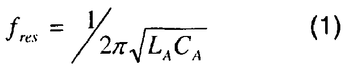
- the capacitance C A comprises a trim capacitor, as is illustrated in Figure 2 , for calibrating the LC resonator 2 according to formula (1) to the desired maximum resonance frequency at manufacturing time of the electrical apparatus 1.
- the tuning module 5 comprises a variable capacitance C T for tuning the LC resonator 2 which is connected in parallel to the LC resonator 2. Furthermore the tuning module 5 comprises memories F max and F min for storing a coded value of a maximum resonance frequency and a coded value of a minimum resonance frequency, respectively, and computing means 3.
- the memories F max and F min are preferably non-volatile memories, for example, EPROM or EEPROM.
- the computing means 3 are preferably implemented as non-programmable logic circuits. Alternatively, the computing means can be implemented by means of programmable logic circuits or by means of a combination of a processor and program code.
- the tuning module 5 comprises an interface E for receiving a coded value of a target resonance frequency f t .
- the coded value of the target resonance frequency f t can be input by means of an operating element, such as a dial, or by means of a wireless receiver receiving the coded value of the target resonance frequency f t via electromagnetic waves from an external remote control.
- the interface E may also be part of a hard wired or programmable core command unit of the device 1. This core command unit may be provided with the input means mentioned above, e.g. with operating elements or wireless receivers, or else, the target resonance frequency f t may be generated within the core command unit.
- the values of the frequencies can be coded as binary frequency codes or as decimal values or according to another coding scheme.
- the computing means 3 compute a tuning code B for adjusting the value of the tuning capacitance C T .
- the tuning code B output by the computing means 3 is passed to the tuning capacitance C T .
- the tuning capacitance C T comprises a capacitive varactor diode connected to a D/A-converter (Digital/Analog) receiving the tuning code B output by the computing means 3.
- the separate capacitors C n-1 , ..., C 2 , C 1 , C 0 can each be selectively connected in parallel to the LC resonator 2 by closing its associated switch T n-1 , ..., T 2 , T 1 , T 0 or disconnected by opening its associated switch T n-1 , ..., T 2 , T 1 , T 0 , respectively.
- the control gates of the switches T n-1 , ..., T 2 , T 1 , T 0 are connected to the outputs B n-1 , ..., B 2 , B 1 , B 0 of the computing means 3, each output B n-1 , ..., B 2 , B 1 , B 0 representing one bit of the tuning code B.
- the tuning code B is a binary code
- the values of the separate capacitors C n-1 , ..., C 2 , C 1 , C 0 are binary weighted.
- each separate capacitor C n-1 , ..., C 2 , C 1 , C 0 corresponds to the binary weight of the bit of the tuning code represented on the output B n-1 , ..., B 2 , B 1 , B 0 that is controlling the switch T n-1 , ..., T 2 , T 1 , T 0 connected to the respective separate capacitor C n-1 , ..., C 2 , C 1 , C 0 .
- the total value of the capacitance of the separate capacitors C n-1 , ..., C 2 , C 1 , C 0 connected in parallel to the LC resonator 2 corresponds to the value of the binary tuning code B output by the computing means 3.
- the tuning module 5 is preferably implemented as an integrated circuit on a chip.
- the separate capacitors C n-1 , ..., C 2 , C 1 , C 0 , the switches T n-1 , ..., T 2 , T 1 , T 0 , the computing means 3 and the memories F max and F min are manufactured in CMOS (Complementary Metal-Oxide-Semiconductor) technology.
- CMOS Complementary Metal-Oxide-Semiconductor
- the LC resonator 2 is calibrated to a desired maximum resonance frequency by adjusting the value of the capacitance C A .
- the calibrated maximum resonance frequency of the LC resonator 2 is measured by means of an external measuring device and stored as a coded value in the memory F max of the tuning module 5. From the external measuring device, the coded value of the maximum resonance frequency can be stored in the memory F max via the interface E, for example.
- a target resonance frequency f t is input through the interface E to the computing means 3.
- the computing means 3 retrieve the coded value of the maximum resonance frequency stored in the memory F max and the coded value of the minimum resonance frequency stored in the memory F min , and compute a tuning code B as an interpolation between the coded value of the maximum resonance frequency and the coded value of the minimum resonance frequency for the received coded value of the target resonance frequency f t .
- the value of the tuning capacitance C T is adjusted according to the computed tuning code B, and the resonance frequency of the LC resonator 2 is tuned to the target resonance frequency f t according to formula (2).
- the LC resonator 2 can be tuned to any intermediate resonance frequency in the range from f min to f max by connecting the separate capacitors C n-1 , ..., C 2 , C 1 , C 0 in parallel to the LC resonator 2 according to the bits B[n-1:0] of the tuning code B.
Landscapes
- Engineering & Computer Science (AREA)
- Computer Networks & Wireless Communication (AREA)
- Computer Hardware Design (AREA)
- Microelectronics & Electronic Packaging (AREA)
- Physics & Mathematics (AREA)
- General Physics & Mathematics (AREA)
- Theoretical Computer Science (AREA)
- Filters And Equalizers (AREA)
- Networks Using Active Elements (AREA)
- Magnetic Resonance Imaging Apparatus (AREA)
- Transmitters (AREA)
- Input Circuits Of Receivers And Coupling Of Receivers And Audio Equipment (AREA)
Description
- The present invention relates to a method and an integrated circuit for tuning an LC resonator and to an electrical apparatus comprising an LC resonator. Specifically, the present invention relates to a method and an integrated circuit for tuning an LC resonator and to an electrical apparatus comprising an LC resonator, which all use a variable capacitance for tuning the LC resonator.
- Tuning of LC resonators is often required for LC resonators that are part of a load circuit of a pre-amplifier or an oscillator, for example. Particularly, LC resonators with antenna coils serving as antennas for radio receivers require tuning when the receivers cover a wider frequency range than the antennas.
- Miniaturised antennas, respectively antenna coils, with geometrical dimensions that are small compared to the wavelength of received signals generally have a high quality factor Q. On the one hand, the sensitivity of a complete receiver system, comprising a radio receiver and an antenna connected to the receiver, is proportional to the quality factor Q of the antenna. On the other hand, the 3dB bandwidth of an antenna is inversely proportional to the quality factor Q of the antenna. For example, an antenna with a quality factor of Q=100, has a 3dB bandwidth of only ∼2 MHz at a frequency of 200 MHz. Therefore, the 3dB bandwidth of a miniaturised antenna is generally much smaller than the tuning range of the receiver.
- Consequently, in order to cover the entire frequency range of the receiver with one single antenna, the antenna needs to be tuned when the signal frequency is changed. Typically, antennas are tuned by means of a variable capacitance connected in parallel to the antenna.
- In formula (1) the resonance frequency fres of an LC resonator comprising an antenna coil LA and a parallel tuning capacitance CA is defined:
- As indicated in formula (2), the resonance frequency fres of the LC resonator can be modified by adding an additional tuning capacitance CT in parallel:

- In the
patent US 4,862,516 a system for automatically tuning the antenna of a miniature portable communications device is described. According toUS 4,862,516 the antenna is tuned by varying the capacitance of a varactor diode connected in parallel to the antenna. The system according toUS 4,862,516 is based on the transmission of a tuning mode signal combined with active control of the tuning means for obtaining a maximum signal. The magnitude of the received signal is measured, a tuning control signal is generated and supplied to a D/A converter to effect tuning of the antenna by monitoring the variations in the magnitude of the received signal. The transmission of a tuning mode signal according toUS 4,862,516 requires a special transmitter. Generally, the transmission of a tuning signal limits the cross-compatibility between different transmitter-receiver systems as the accurate calibration of the receiver tuning circuit has to be known by the transmitter. In principle, each transmitter-receiver pair would need to be calibrated together. Moreover, owing to the dependency on receiving the special tuning mode signal, it is not possible to have the system automatically and autonomously scan a frequency range and tune the antenna. Finally, active tuning control with a feedback path requires a relatively complex system. - A similar method for active tuning control with feedback is described in the
patent US 5,438,688 . According toUS 5,438,688 the signal strength of the received signal is measured and from the measured signal strength an antenna tuning voltage is derived for controlling the tuning means. According toUS 5, 438, 688 a predictor value for coarse tuning is obtained from previous tuning cycles. - In the
patent US 5,589,844 another active tuning control system is described wherein the capacitance of capacitive elements is adjusted electromechanically. According toUS 5,589,844 initial impedance values are determined for each frequency in an operating range and stored in a non-volatile memory. - In the
patent US 5,491,715 another method for actively tuning an antenna based on a feedback signal is described wherein the antenna is tuned to a desired frequency by modifying the value of capacitors connected in parallel to the antenna. - All antenna tuning systems based on active control with a feedback path have the disadvantage of requiring relatively complex active controlling means. When integrating the antenna tuning system on a chip, the complex analog circuitry used for the active controlling means increases both the size of the silicon surface and the power consumption of the chip. Furthermore, whenever the frequency is changed, tuning systems based on active control require time for tuning optimisation which is particularly unfavorable, i.e. time-consuming, when a channel scan is performed. Moreover, if no carrier is present on a channel, the scan could end in an infinite loop, the receiver trying to optimise on a non-existing signal. Similarly, if there is no signal available before tuning, because the antenna is untuned, tuning the antenna by means of an active control mechanism is difficult as the signal to optimise is not available and needs first "to be found."
- It is an object of this invention to provide a method, an integrated circuit and an electrical apparatus which are capable of tuning an LC resonator and which do not have the disadvantages of the prior art. In particular, it is an object of the present invention to provide a method, an integrated circuit and an electrical apparatus capable of automatically tuning a miniaturised antenna over a large frequency band without using active control mechanisms with feedback.
- According to the present invention, these objects are achieved particularly through the features of the independent claims. In addition, further advantageous embodiments follow from the dependent claims and the description.
- A variable capacitance for tuning the LC resonator is connected in parallel to the LC resonator. In the preferred application, the inductance of the LC resonator comprises an antenna coil, particularly a miniaturised antenna coil.
- According to the present invention, the above-mentioned objects are particularly achieved in that at manufacturing time, a maximum resonance frequency of the LC resonator is measured when the variable capacitance connected in parallel to the LC resonator is set to its minimum value and a coded value of the measured maximum resonance frequency is stored in a first memory of a tuning module, and a minimum resonance frequency of the LC resonator is measured when the variable capacitance is set to its maximum value and a coded value of the measured minimum resonance frequency is stored in a second memory of the tuning module. The first and second memories of the tuning module are preferably non-volatile memories. At operations time, a tuning code for setting the variable capacitance to a value that results in a target resonance frequency of the LC resonator is computed as an interpolation between the coded value stored in the first memory and the coded value stored in the second memory for a coded value of the target resonance frequency, and the value of the variable capacitance is adjusted in accordance with the value of the computed tuning code. Advantageously, the LC resonator and correspondingly a miniaturised antenna can be tuned without using active control mechanisms with feedback; there is no need for measuring signal strength and no special tuning mode signal is necessary. The LC resonator and correspondingly the miniaturised antenna can be tuned in the time it takes to perform one single computation. Finally, owing to their reduced complexity, the module for tuning the LC resonator and correspondingly for tuning the miniaturised antenna can be fully integrated on a chip, for example through a CMOS process.
- In a preferred embodiment, the variable capacitance connected in parallel to the LC resonator comprises several separate capacitors, and the value of the variable capacitance is adjusted by selectively closing switches associated with each of the separate capacitors in accordance with the value of the determined tuning code. Preferably, the switches are implemented as transistors, and the computing means, the transistors and the separate capacitors are integrated on a chip, for example a CMOS chip. Latest CMOS technologies make it possible to build MOS transistor switches with sufficiently low on-resistance at low supply voltages. Furthermore, these MOS transistors have small parasitic capacitances which makes them appropriate for applications in the VHF and UHF frequency range.
- In the preferred embodiment the tuning code is a binary code, the values of the separate capacitors are binary weighted, and the bits composing the tuning code are assigned to the switches associated with the separate capacitors such that the binary weight of each bit corresponds to the binary weight of the separate capacitor associated with the switch. Using a binary tuning code and binary weighted values of the separate capacitors makes possible an extremely simple interconnection of the computing means and the variable capacitance, thereby reducing size and power consumption of the tuning module or its corresponding integrated circuit, respectively.
- Preferably, the tuning code is computed as a linear interpolation, comprising computing a ratio of the difference between the coded value stored in the first memory and the coded value of the target resonance frequency and of the difference between the coded value stored in the first memory and the coded value stored in the second memory. Computing the tuning code as a linear interpolation makes it possible to use computing means of very simple complexity, thereby reducing size and power consumption of the tuning module or its corresponding integrated circuit, respectively.
- Preferably, the LC resonator comprises a trim capacitor for a one-time simple and straightforward calibration of the LC resonator at manufacturing time. The LC resonator can be calibrated to a desired maximum resonance frequency by disconnecting all the separate capacitors of the variable capacitance and by setting the trim capacitor to the appropriate calibration value. The one-time calibration with local calibration means makes transmission of special tuning signals unnecessary.
- The present invention will be explained in more detail, by way of example, with reference to the drawings in which:
-
Figure 1 shows a block diagram illustrating an electrical apparatus with an LC resonator connected to a module for tuning the LC resonator, which module comprises a variable capacitance controlled by computing means. -
Figure 2 shows a block diagram illustrating an LC resonator connected to a circuit for tuning the LC resonator, which circuit comprises several separate capacitors selectively connectable in parallel to the LC resonator. - In the
Figures 1 and2 , thereference numeral 1 refers to an electrical apparatus comprising anLC resonator 2, atuning module 5 and anoptional radio receiver 4, connected to theLC resonator 2. As is illustrated inFigures 1 and2 , theLC resonator 2 comprises an inductance LA and a capacitance CA. In a preferred application, the inductance LA is an antenna coil, particularly a miniaturised antenna coil, connected to theradio receiver 4. The geometrical dimensions of a miniaturised antenna coil are small compared to the wavelength of received radio signals. The miniaturised antenna coil of the inductance LA is dimensioned for use in preferred applications in the VHF (Very High Frequency, 30 - 300 MHz) or UHF (Ultra High Frequency, 300 MHz - 3 GHz) frequency range. Examples of miniaturised antennas used in preferred applications in the VHF frequency range are air coils with a diameter of approximately 4 mm and with typically 2 to 5 windings or coils wound on ferrite rods with approximate dimensions of (7x3x2) mm3. Preferably, the capacitance CA comprises a trim capacitor, as is illustrated inFigure 2 , for calibrating theLC resonator 2 according to formula (1) to the desired maximum resonance frequency at manufacturing time of theelectrical apparatus 1. - As is illustrated in
Figures 1 and2 , thetuning module 5 comprises a variable capacitance CT for tuning theLC resonator 2 which is connected in parallel to theLC resonator 2. Furthermore thetuning module 5 comprises memories Fmax and Fmin for storing a coded value of a maximum resonance frequency and a coded value of a minimum resonance frequency, respectively, and computing means 3. The memories Fmax and Fmin are preferably non-volatile memories, for example, EPROM or EEPROM. The computing means 3 are preferably implemented as non-programmable logic circuits. Alternatively, the computing means can be implemented by means of programmable logic circuits or by means of a combination of a processor and program code. Finally, thetuning module 5 comprises an interface E for receiving a coded value of a target resonance frequency ft. The coded value of the target resonance frequency ft can be input by means of an operating element, such as a dial, or by means of a wireless receiver receiving the coded value of the target resonance frequency ft via electromagnetic waves from an external remote control. Alternatively, the interface E may also be part of a hard wired or programmable core command unit of thedevice 1. This core command unit may be provided with the input means mentioned above, e.g. with operating elements or wireless receivers, or else, the target resonance frequency ft may be generated within the core command unit. The values of the frequencies can be coded as binary frequency codes or as decimal values or according to another coding scheme. - As will be explained later in detail, the computing means 3 compute a tuning code B for adjusting the value of the tuning capacitance CT. As is illustrated in
Figure 1 , the tuning code B output by the computing means 3 is passed to the tuning capacitance CT. - In a possible embodiment, the tuning capacitance CT comprises a capacitive varactor diode connected to a D/A-converter (Digital/Analog) receiving the tuning code B output by the computing means 3.
- In the preferred embodiment illustrated in
Figure 2 , the tuning capacitance CT comprises several separate capacitors Cn-1, ..., C2, C1, C0. Each one of the separate capacitors Cn-1, ..., C2, C1, C0 is connected in series to an associated switch Tn-1, ..., T2, T1, T0. The switches Tn-1, ..., T2, T1, T0 are preferably transistors. The separate capacitors Cn-1, ..., C2, C1, C0 can each be selectively connected in parallel to theLC resonator 2 by closing its associated switch Tn-1, ..., T2, T1, T0 or disconnected by opening its associated switch Tn-1, ..., T2, T1, T0, respectively. The control gates of the switches Tn-1, ..., T2, T1, T0 are connected to the outputs Bn-1, ..., B2, B1, B0 of the computing means 3, each output Bn-1, ..., B2, B1, B0 representing one bit of the tuning code B. A high value (ON: bit="1") on an output Bn-1, ..., B2, B1, B0 closes, and a low value (OFF: bit="0") on an output Bn-1, ..., B2, B1, B0 opens, the respective switch Tn-1, ..., T2, T1, T0. Preferably, the tuning code B is a binary code, and the values of the separate capacitors Cn-1, ..., C2, C1, C0 are binary weighted. The binary weight of each separate capacitor Cn-1, ..., C2, C1, C0 corresponds to the binary weight of the bit of the tuning code represented on the output Bn-1, ..., B2, B1, B0 that is controlling the switch Tn-1, ..., T2, T1, T0 connected to the respective separate capacitor Cn-1, ..., C2, C1, C0. Hence the total value of the capacitance of the separate capacitors Cn-1, ..., C2, C1, C0 connected in parallel to theLC resonator 2 corresponds to the value of the binary tuning code B output by the computing means 3. - The
tuning module 5 is preferably implemented as an integrated circuit on a chip. Preferably, the separate capacitors Cn-1, ..., C2, C1, C0, the switches Tn-1, ..., T2, T1, T0, the computing means 3 and the memories Fmax and Fmin are manufactured in CMOS (Complementary Metal-Oxide-Semiconductor) technology. Thetuning module 5 and theradio receiver 4 can be implemented on one common chip or on separate chips. - At manufacturing time of the
electrical apparatus 1, the variable capacitance CT is set to its minimum value, i.e. in the preferred embodiment, all the separate capacitors Cn-1, ..., C2, C1, C0 are disconnected by opening all the switches Tn-1, ..., T2, T1, T0 (i.e. tuning code B='0...000'). Then theLC resonator 2 is calibrated to a desired maximum resonance frequency by adjusting the value of the capacitance CA. The calibrated maximum resonance frequency of theLC resonator 2 is measured by means of an external measuring device and stored as a coded value in the memory Fmax of thetuning module 5. From the external measuring device, the coded value of the maximum resonance frequency can be stored in the memory Fmax via the interface E, for example. - Thereafter, the variable capacitance CT is set to its maximum value, i.e. in the preferred embodiment, all the separate capacitors Cn-1, ..., C2, C1, C0 are connected in parallel to the LC resonator by closing all the switches Tn-1, ..., T2, T1, T0 (i.e. tuning code B='1...111'). At this setting, the minimum resonance frequency of the
LC resonator 2 is measured and stored as a coded value in the memory Fmin of thetuning module 5. From the external measuring device, the coded value of the minimum resonance frequency can be stored in the memory Fmin via the interface E, for example. - During operation of the
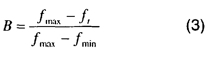
electrical apparatus 1, a target resonance frequency ft is input through the interface E to the computing means 3. The computing means 3 retrieve the coded value of the maximum resonance frequency stored in the memory Fmax and the coded value of the minimum resonance frequency stored in the memory Fmin, and compute a tuning code B as an interpolation between the coded value of the maximum resonance frequency and the coded value of the minimum resonance frequency for the received coded value of the target resonance frequency ft. - In its simplest form the computation can be a linear interpolation according to formula (3), fmax and fmin representing the values stored in the memories Fmax and Fmin:
- In the embodiment where the capacitance CT comprises several separate capacitors Cn-1, ..., C2, C1, C0, the value of the variable capacitance CT corresponds to the sum of all the separate capacitors Cn-1, ..., C2, C1, C0 connected in parallel to the
LC resonator 2, as defined in formula (4), wherein B[i] corresponds to the bits of the tuning code B on the outputs Bn-1, ..., B2, B1, B0: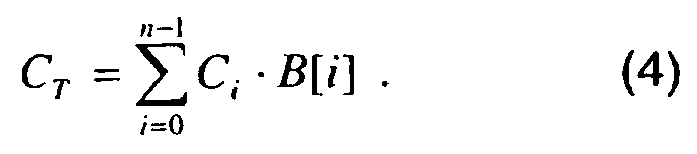
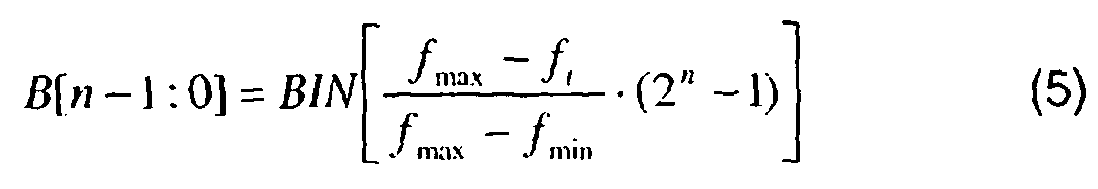
- In the case of binary coding of the frequency values fmax, fmin and ft, the tuning code B, having the most significant bit B[n-1] and the least significant bit B[0], is determined according to formula (5), wherein BIN[x] is the binary expression of x:
- The tuning code B[n-1:0] computed by the computing means 3 is assigned to the outputs Bn-1, ..., B2, B1, B0, the switches Tn-1, ..., T2, T1, T0 controlled by an output Bn-1, ..., B2, B1, B0 carrying a bit with a high value get closed, and the associated separate capacitors Cn-1, ..., C2, C1, C0 are connected in parallel to the
LC resonator 2. - Consequently, the value of the tuning capacitance CT is adjusted according to the computed tuning code B, and the resonance frequency of the
LC resonator 2 is tuned to the target resonance frequency ft according to formula (2). TheLC resonator 2 can be tuned to any intermediate resonance frequency in the range from fmin to fmax by connecting the separate capacitors Cn-1, ..., C2, C1, C0 in parallel to theLC resonator 2 according to the bits B[n-1:0] of the tuning code B. - The resulting total capacitance Ctotal comprising the capacitance CA and the variable capacitance CT is defined in formula (6):

- The resulting resonance frequency fres of the LC resonator is given in formula (7):

- Because of the linearisation of the function according to formula (1) in a limited frequency range, only a small error results. For example, using ten bits for the frequency coding and using five separate capacitors (n=5) for tuning an
LC resonator 2 with an antenna coil will result in an attenuation of the antenna smaller than one decibel (<1dB), which is more or less negligible.
Claims (26)
- Method for tuning an LC resonator (2) comprising connecting a variable capacitance (CT) in parallel to the LC resonator (2), the method further comprising the steps of:measuring a maximum resonance frequency of the LC resonator (2), the variable capacitance (CT) being set to its minimum value, and storing a coded value of the maximum resonance frequency in a first memory (Fmax),measuring a minimum resonance frequency of the LC resonator (2), the variable capacitance (CT) being set to its maximum value, and storing a coded value of the minimum resonance frequency in a second memory (Fmin),computing a tuning code (B) for setting the variable capacitance (CT) to a value that results in a target resonance frequency (ft) of the LC resonator, the tuning code (B) being computed as an interpolation between the coded value stored in the first memory (Fmax) and the coded value stored in the second memory (Fmin) for a coded value of the target resonance frequency (ft), andadjusting the value of the variable capacitance (CT) in accordance with the value of the computed tuning code (B).
- Method according to claim 1, characterised in that adjusting the value of the variable capacitance (CT) in accordance with the value of the computed tuning code (B) is done by connecting selected separate capacitors (Cn-1, ..., C2, C1, C0) of the variable capacitance (CT) in parallel to the LC resonator (2) by closing switches (Tn-1, ..., T2, T1, T0) associated with each of the selected separate capacitors (Cn-1, ..., C2, C1, C0) in accordance with the value of the computed tuning code (B).
- Method according to claim 2, characterised in that a binary code is used for the tuning code (B), in that the values of the separate capacitors (Cn-1, ..., C2, C1, C0) are binary weighted, and in that bits composing the tuning code (B) are assigned to the switches (Tn-1, ..., T2, T1, T0) associated with the separate capacitors (Cn-1, ..., C2, C1, C0) such that the binary weight of each bit corresponds to the binary weight of the separate capacitor (Cn-1, ...., C2, C1, C0) associated with the switch (Tn-1, ..., T2, T1, T0).
- Method according to one of the claims 1 to 3, characterised in that the tuning code (B) is computed as a linear interpolation, comprising computing a ratio of the difference between the coded value stored in the first memory (Fmax) and the coded value of the target resonance frequency (ft) and of the difference between the coded value stored in the first memory (Fmax) and the coded value stored in the second memory (Fmin).
- Method according to one of the claims 2 to 4, characterised in that it further comprises prior to measuring the maximum resonance frequency of the LC resonator (2), disconnecting all the separate capacitors (Cn-1, ..., C2, C1, C0) of the variable capacitance (CT) and setting a trim capacitor of the LC resonator (2) to a calibration value that results in a desired maximum resonance frequency of the LC resonator (2), and prior to measuring the minimum resonance frequency of the LC resonator (2), connecting all the separate capacitors (Cn-1, ..., C2, C1, C0) of the variable capacitance (CT) in parallel to the LC resonator (2).
- Method according to one of the claims 1 to 5, characterised in that it comprises measuring the maximum resonance frequency and the minimum resonance frequency at manufacturing time of an electrical apparatus (1) comprising the LC resonator (2) and storing the coded values of the measured maximum resonance frequency and of the measured minimum resonance frequency in non-volatile memories.
- Method according to one of the claims 1 to 6, characterised in that an antenna coil, particularly a miniaturised antenna coil, is used as an inductance (LA) of the LC resonator (2).
- Method according to one of the claims 2 to 6, characterised in that transistors are used for the switches (Tn-1, ... , T2, T1, T0), and in that the transistors and the separate capacitors (Cn-1, ..., C2, C1, C0) of the variable capacitance (CT) are integrated on a chip.
- Method according to claim 8, characterised in that the separate capacitors (Cn-1, ..., C2, C1, C0) of the variable capacitance (CT) are integrated on a CMOS chip, and in that MOS transistors are used for the switches (Tn-1, ..., T2, T1, T0).
- Method according to one of the claims 1 to 9, characterised in that an LC resonator (2) having a resonance frequency in the VHF or UHF frequency range is used.
- Electrical apparatus (1) comprising an LC resonator (2) and a variable capacitance (CT) connected in parallel to the LC resonator (2), characterised
in that the electrical apparatus (1) comprises a first memory (Fmax), having stored therein a coded value of a maximum resonance frequency of the LC resonator (2) measured for the variable capacitance (CT) set to its minimum value,
in that the electrical apparatus (1) comprises a second memory (Fmin), having stored therein a coded value of a minimum resonance frequency of the LC resonator (2) measured for the variable capacitance (CT) set to its maximum value,
in that the electrical apparatus (1) comprises computing means (3) for computing a tuning code (B) for setting the variable capacitance (CT) to a value that results in a target resonance frequency (ft) of the LC resonator (2), the computing means (3) being connected to the first memory (Fmax) and to the second memory (Fmin), and the tuning code (B) being computed as an interpolation between the coded value stored in the first memory (Fmax) and the coded value stored in the second memory (Fmin) for a coded value of the target resonance frequency (ft), and
in that the electrical apparatus (1) comprises means for adjusting the value of the variable capacitance (CT) in accordance with the value of the computed tuning code (B). - Electrical apparatus (1) according to claim 11, characterised in that the variable capacitance (CT) comprises several separate capacitors (Cn-1, ..., C2, C1, C0) and switches (Tn-1, ..., T2, T1, T0) associated with each of the separate capacitors (Cn-1, ..., C2, C1, C0) for selectively connecting the separate capacitors (Cn-1, ..., C2, C1, C0) in parallel to the LC resonator (2), and in that the electrical apparatus (1) comprises means for connecting selected ones of the separate capacitors (Cn-1, ..., C2, C1, C0) in parallel to the LC resonator (2) by closing the switches (Tn-1, ..., T2, T1, T0) associated with the selected separate capacitors (Cn-1, ..., C2, C1, C0) in accordance with the value of the computed tuning code (B).
- Electrical apparatus (1) according to claim 12, characterised in that the tuning code (B) is a binary code, in that the values of the separate capacitors (Cn-1, ..., C2, C1, C0) are binary weighted, and in that the computing means (3) and the switches (Tn-1, ..., T2, T1, T0) are connected, each connection between the computing means (3) and one of the switches (Tn-1, ..., T2, T1, T0) carrying a bit of the tuning code (B), the binary weight of the bit corresponding to the binary weight of the separate capacitor (Cn-1, ..., C2, C1, C0) associated with the switch.
- Electrical apparatus (1) according to one of the claims 11 to 13, characterised in that the computing means (3) of the electrical apparatus (1) are designed to compute the tuning code (B) as a linear interpolation, computing a ratio of the difference between the coded value stored in the first memory (Fmax) and the coded value of the target resonance frequency (ft) and of the difference between the coded value stored in the first memory (Fmax) and the coded value stored in the second memory (Fmin).
- Electrical apparatus (1) according to one of the claims 12 to 14, characterised in that, the LC resonator (2) comprises a trim capacitor for calibrating the LC resonator (2) to a desired maximum resonance frequency of the LC resonator (2) when all the separate capacitors (Cn-1, ..., C2, C1, C0) of the variable capacitance (CT) are disconnected.
- Electrical apparatus (1) according to one of the claims 11 to 15, characterised in that the first memory (Fmax) and the second memory (Fmin) are non-volatile memories.
- Electrical apparatus (1) according to one of the claims 11 to 16, characterised in that the LC resonator (2) comprises an antenna coil, particularly a miniaturised antenna coil, and in that the electrical apparatus (1) comprises a radio receiver (4) connected to the antenna coil.
- Electrical apparatus (1) according to one of the claims 12 to 17, characterised in that the switches (Tn-1, ..., T2, T1, T0) are transistors, and in that the computing means (3), the transistors and the separate capacitors (Cn-1, ..., C2, C1, C0) of the variable capacitance (CT) are integrated on a chip.
- Electrical apparatus (1) according to claim 18, characterised in that the separate capacitors (Cn-1, ..., C2, C1, C0) of the variable capacitance (CT) are integrated on a CMOS chip, and in that the switches (Tn-1 , ..., T2, T1, T0) are MOS transistors.
- Electrical apparatus (1) according to one of the claims 11 to 19, characterised in that the LC resonator (2) has a resonance frequency in the VHF or UHF frequency range.
- Integrated circuit comprising a variable capacitance (CT) for tuning an external LC resonator (2), characterised
in that the integrated circuit comprises a first memory (Fmax), for storing therein a coded value of a maximum resonance frequency of the external LC resonator (2) measured in the state of the integrated circuit being connected in parallel to the LC resonator (2), for the variable capacitance (CT) set to its minimum value,
in that the integrated circuit comprises a second memory (Fmin), for storing therein a coded value of a minimum resonance frequency of the external LC resonator (2) measured in the state of the integrated circuit being connected in parallel to the LC resonator (2), for the variable capacitance (CT) set to its maximum value,
in that the integrated circuit comprises computing means (3) for computing a tuning code (B) for setting the variable capacitance (CT) to a value that results in a target resonance frequency (ft) of the external LC resonator (2) in the state of the integrated circuit being connected in parallel to the LC resonator (2), the computing means (3) being connected to the first memory (Fmax) and to the second memory (Fmin), and the tuning code (B) being computed as an interpolation between the coded value stored in the first memory (Fmax) and the coded value stored in the second memory (Fmin) for a coded value of the target resonance frequency (ft), and
in that the integrated circuit comprises means for adjusting the value of the variable capacitance (CT) in accordance with the value of the computed tuning code (B). - Integrated circuit according to claim 21, characterised in that the variable capacitance (CT) of the integrated circuit comprises several separate capacitors (Cn-1, ..., C2, C1, C0) and switches (Tn-1 ,..., T2, T1, T0) associated with each of the separate capacitors (Cn-1, ..., C2, C1, C0) for selectively connecting the separate capacitors (Cn-1, ..., C2, C1, C0) in parallel to the external LC resonator (2), and in that the integrated circuit comprises means for connecting selected ones of the separate capacitors (Cn-1, ..., C2, C1, C0) in parallel to the external LC resonator (2) by closing the switches (Tn-1, ..., T2, T1, T0) associated with the selected separate capacitors (Cn-1, ..., C2, C1, C0) in accordance with the value of the computed tuning code (B).
- Integrated circuit according to claim 22, characterised in that the tuning code (B) is a binary code, in that the values of the separate capacitors (Cn-1, ..., C2, C1, C0) are binary weighted, and in that the computing means (3) and the switches (Tn-1, ..., T2, T1, T0) are connected, each connection between the computing means (3) and one of the switches (Tn-1, ..., T2, T1, T0) carrying a bit of the tuning code (B), the binary weight of the bit corresponding to the binary weight of the separate capacitor (Cn-1, C2, C1, C0) associated with the switch.
- Integrated circuit according to one of the claims 21 or 23, characterised in that the computing means (3) are designed to compute the tuning code (B) as a linear interpolation, computing a ratio of the difference between the coded value stored in the first memory (Fmax) and the coded value of the target resonance frequency (ft) and of the difference between the coded value stored in the first memory (Fmax) and the coded value stored in the second memory (Fmin).
- Integrated circuit according to one of the claims 21 to 24, characterised in that the first memory (Fmax) and the second memory (Fmin) are non-volatile memories.
- Integrated circuit according to one of the claims 21 to 25, characterised in that the separate capacitors (Cn-1, ..., C2, C1, C0) are integrated on a CMOS chip, and in that the switches (Tn-1,..., T2, T1, T0) are MOS transistors.
Priority Applications (7)
| Application Number | Priority Date | Filing Date | Title |
|---|---|---|---|
| EP03405006A EP1437829B1 (en) | 2003-01-09 | 2003-01-09 | Method and integrated circuit for tuning an LC resonator and electrical apparatus comprising an LC resonator |
| DK03405006T DK1437829T3 (en) | 2003-01-09 | 2003-01-09 | Method and integrated circuit for tuning an LC resonator and electrical apparatus comprising an LC resonator |
| DE60319665T DE60319665T2 (en) | 2003-01-09 | 2003-01-09 | Method and integrated circuit for tuning an LC resonator and electrical device containing an LC resonator |
| US10/339,528 US20040137865A1 (en) | 2003-01-09 | 2003-01-09 | Method and integrated circuit for tuning an LC resonator and electrical apparatus comprising an LC resonator |
| CA002448316A CA2448316A1 (en) | 2003-01-09 | 2003-11-05 | Method and integrated circuit for tuning an lc resonator and electrical apparatus comprising an lc resonator |
| IL15876303A IL158763A0 (en) | 2003-01-09 | 2003-11-06 | Method and integrated circuit for tuning an lc resonator and electrical apparatus comprising an lc resonator |
| JP2003414257A JP4283657B2 (en) | 2003-01-09 | 2003-12-12 | LC resonator tuning method and electric device having LC resonator |
Applications Claiming Priority (2)
| Application Number | Priority Date | Filing Date | Title |
|---|---|---|---|
| EP03405006A EP1437829B1 (en) | 2003-01-09 | 2003-01-09 | Method and integrated circuit for tuning an LC resonator and electrical apparatus comprising an LC resonator |
| US10/339,528 US20040137865A1 (en) | 2003-01-09 | 2003-01-09 | Method and integrated circuit for tuning an LC resonator and electrical apparatus comprising an LC resonator |
Publications (2)
| Publication Number | Publication Date |
|---|---|
| EP1437829A1 EP1437829A1 (en) | 2004-07-14 |
| EP1437829B1 true EP1437829B1 (en) | 2008-03-12 |
Family
ID=33312116
Family Applications (1)
| Application Number | Title | Priority Date | Filing Date |
|---|---|---|---|
| EP03405006A Expired - Lifetime EP1437829B1 (en) | 2003-01-09 | 2003-01-09 | Method and integrated circuit for tuning an LC resonator and electrical apparatus comprising an LC resonator |
Country Status (7)
| Country | Link |
|---|---|
| US (1) | US20040137865A1 (en) |
| EP (1) | EP1437829B1 (en) |
| JP (1) | JP4283657B2 (en) |
| CA (1) | CA2448316A1 (en) |
| DE (1) | DE60319665T2 (en) |
| DK (1) | DK1437829T3 (en) |
| IL (1) | IL158763A0 (en) |
Families Citing this family (27)
| Publication number | Priority date | Publication date | Assignee | Title |
|---|---|---|---|---|
| DE102004037637A1 (en) * | 2004-08-02 | 2006-03-16 | Deutsche Thomson-Brandt Gmbh | Receiver circuit and control method |
| GB0506887D0 (en) | 2005-04-05 | 2005-05-11 | Rokos George H S | Improvement to tuning control |
| GB2425007B (en) * | 2004-09-20 | 2010-11-17 | George Hedley Storm Rokos | Tuning control arrangement |
| US20080211621A1 (en) | 2005-05-23 | 2008-09-04 | Nxp B.V. | Electronic Communication System, in Particular Authentication Control System, as Well as Corresponding Method |
| US20070257699A1 (en) * | 2006-04-20 | 2007-11-08 | Moises Cases | Multi-memory module circuit topology |
| DE602006002743D1 (en) * | 2006-07-06 | 2008-10-23 | Dibcom | Integrated tuning circuit with antenna control unit |
| US20080079587A1 (en) * | 2006-09-29 | 2008-04-03 | Ahmadreza Rofougaran | Method And System For Utilizing Magnetic On-Chip Coil For Ultra High Frequency (UHF) |
| US8081940B2 (en) * | 2006-09-29 | 2011-12-20 | Broadcom Corporation | Method and system for dynamically tuning and calibrating an antenna using an on-chip digitally controlled array of capacitors |
| ES2326298B1 (en) * | 2006-11-27 | 2010-07-05 | Datamars, S.A. | ELECTRONIC DEVICE FOR RADIO IDENTIFICATION FREQUENCY AND METHOD FOR THE ADJUSTMENT OF THE FREQUENCY OF RESONANCE OF SUCH ELECTRONIC DEVICE. |
| JP4310661B2 (en) * | 2007-02-05 | 2009-08-12 | ソニー株式会社 | IC for tuning circuit and receiving circuit using the same |
| JP4693801B2 (en) * | 2007-03-05 | 2011-06-01 | 日本無線株式会社 | Capacitor switching circuit |
| JP2009049813A (en) * | 2007-08-21 | 2009-03-05 | Sanyo Electric Co Ltd | Semiconductor device for radio tuner and manufacturing method thereof |
| JP5023965B2 (en) * | 2007-10-26 | 2012-09-12 | ソニー株式会社 | Reader / writer device and non-contact data carrier system |
| JP4557086B2 (en) * | 2008-06-24 | 2010-10-06 | カシオ計算機株式会社 | Radio wave receiver |
| JP4715926B2 (en) * | 2009-01-14 | 2011-07-06 | カシオ計算機株式会社 | Radio wave receiver |
| JP4816764B2 (en) | 2009-05-28 | 2011-11-16 | カシオ計算機株式会社 | Radio wave receiver |
| US9479225B2 (en) * | 2010-05-13 | 2016-10-25 | Qualcomm Incorporated | Resonance detection and control within a wireless power system |
| TWI418155B (en) | 2011-03-23 | 2013-12-01 | 笙科電子股份有限公司 | Circuit and method for automatically correcting antenna resonance frequency |
| KR101353143B1 (en) * | 2012-03-27 | 2014-01-23 | 삼성전기주식회사 | Hybrid variable capacitor, rf apparatus, method for manufacturing hybrid variable capacitor and method for tuning variable capacitor |
| KR101931256B1 (en) | 2012-07-25 | 2018-12-20 | 삼성전자주식회사 | Wireless power reception apparatus and method |
| CN103151853A (en) * | 2013-04-03 | 2013-06-12 | 天津工业大学 | Wireless power transmission impedance automatic matching device |
| JP6043247B2 (en) * | 2013-07-12 | 2016-12-14 | デクセリアルズ株式会社 | Control circuit, resonance circuit, electronic device, control method, control program, and semiconductor element |
| DE102015005927A1 (en) * | 2015-05-07 | 2016-11-10 | Finepower Gmbh | Device and method for adaptive compensation of a resonant circuit |
| TWI698084B (en) * | 2017-07-14 | 2020-07-01 | 瑞昱半導體股份有限公司 | Oscillator and control method |
| TWI662760B (en) | 2017-08-21 | 2019-06-11 | 國立交通大學 | Resonant magnetic coupling wireless power transfer system with calibration capability of its inductor-capacitor resonant frequencies |
| CN110096167A (en) * | 2019-05-10 | 2019-08-06 | 鲁伯特(北京)教育科技有限公司 | A kind of LC resonance circuit of time writer and the method for proposing high q-factor |
| KR20220017291A (en) | 2020-08-04 | 2022-02-11 | 삼성전기주식회사 | Capacitor circuit and variable capacitance system including the same |
Family Cites Families (19)
| Publication number | Priority date | Publication date | Assignee | Title |
|---|---|---|---|---|
| US4138654A (en) * | 1977-09-12 | 1979-02-06 | Harris Corporation | Digitally tuned circuit including switching of bank capacitors between plural tuned circuits |
| US4481673A (en) * | 1983-03-28 | 1984-11-06 | Rca Corporation | RF Prom tracking for tuners |
| US4623856A (en) * | 1984-06-11 | 1986-11-18 | Motorola, Inc. | Incrementally tuned RF filter having pin diode switched lines |
| US4788543A (en) * | 1986-11-05 | 1988-11-29 | Richard Rubin | Apparatus and method for broadcasting priority rated messages on a radio communications channel of a multiple transceiver system |
| US4920570A (en) * | 1987-12-18 | 1990-04-24 | West Henry L | Modular assistive listening system |
| US5157623A (en) * | 1989-12-30 | 1992-10-20 | Casio Computer Co., Ltd. | Digital filter with dynamically variable filter characteristics |
| DE4327642C2 (en) * | 1993-05-17 | 1998-09-24 | Anatoli Stobbe | Reader for a detection plate |
| JPH07193879A (en) * | 1993-12-27 | 1995-07-28 | Alpine Electron Inc | Survival method of same address unit |
| US5745844A (en) * | 1996-10-04 | 1998-04-28 | Motorola, Inc. | Receiver control in a communication device by antenna de-tuning in strong signal conditions, and method therefor |
| US6212229B1 (en) * | 1998-12-16 | 2001-04-03 | General Dynamics Government Systems Corporation | Adaptive pre-emphasis technique |
| US6317027B1 (en) * | 1999-01-12 | 2001-11-13 | Randy Watkins | Auto-tunning scanning proximity reader |
| US6211745B1 (en) * | 1999-05-03 | 2001-04-03 | Silicon Wave, Inc. | Method and apparatus for digitally controlling the capacitance of an integrated circuit device using mos-field effect transistors |
| GB9916901D0 (en) * | 1999-07-19 | 1999-09-22 | Cambridge Silicon Radio Ltd | Adjustable filter |
| US6198931B1 (en) * | 1999-07-28 | 2001-03-06 | Motorola, Inc. | Method for prioritizing a communication in a wireless communication system |
| US7555263B1 (en) * | 1999-10-21 | 2009-06-30 | Broadcom Corporation | Adaptive radio transceiver |
| US7050781B2 (en) * | 2002-05-16 | 2006-05-23 | Intel Corporation | Self-calibrating tunable filter |
| US6750734B2 (en) * | 2002-05-29 | 2004-06-15 | Ukom, Inc. | Methods and apparatus for tuning an LC filter |
| US6784766B2 (en) * | 2002-08-21 | 2004-08-31 | Raytheon Company | MEMS tunable filters |
| TWI373925B (en) * | 2004-02-10 | 2012-10-01 | Tridev Res L L C | Tunable resonant circuit, tunable voltage controlled oscillator circuit, tunable low noise amplifier circuit and method of tuning a resonant circuit |
-
2003
- 2003-01-09 DK DK03405006T patent/DK1437829T3/en active
- 2003-01-09 DE DE60319665T patent/DE60319665T2/en not_active Expired - Lifetime
- 2003-01-09 US US10/339,528 patent/US20040137865A1/en not_active Abandoned
- 2003-01-09 EP EP03405006A patent/EP1437829B1/en not_active Expired - Lifetime
- 2003-11-05 CA CA002448316A patent/CA2448316A1/en not_active Abandoned
- 2003-11-06 IL IL15876303A patent/IL158763A0/en not_active IP Right Cessation
- 2003-12-12 JP JP2003414257A patent/JP4283657B2/en not_active Expired - Fee Related
Also Published As
| Publication number | Publication date |
|---|---|
| JP2004222249A (en) | 2004-08-05 |
| JP4283657B2 (en) | 2009-06-24 |
| IL158763A0 (en) | 2004-05-12 |
| EP1437829A1 (en) | 2004-07-14 |
| US20040137865A1 (en) | 2004-07-15 |
| DE60319665D1 (en) | 2008-04-24 |
| DK1437829T3 (en) | 2008-07-14 |
| CA2448316A1 (en) | 2004-07-09 |
| DE60319665T2 (en) | 2009-04-02 |
Similar Documents
| Publication | Publication Date | Title |
|---|---|---|
| EP1437829B1 (en) | Method and integrated circuit for tuning an LC resonator and electrical apparatus comprising an LC resonator | |
| US6907234B2 (en) | System and method for automatically tuning an antenna | |
| US6529088B2 (en) | Closed loop antenna tuning system | |
| US7925220B2 (en) | Method and system for matching an integrated FM system to an antenna utilizing on-chip measurement of reflected signals | |
| EP1931051B1 (en) | Method and system for single chip WLAN and Bluetooth radios on a single CMOS substrate | |
| US9002278B2 (en) | Simple automatic antenna tuning system and method | |
| US8145169B2 (en) | Method and system for LNA adjustment to compensate for dynamic impedance matching | |
| EP3068056B1 (en) | Antenna tuning circuit | |
| US8306491B2 (en) | Controlling fine frequency changes in an oscillator | |
| EP1143606A1 (en) | Numerically controlled variable oscillator | |
| WO2003038999A1 (en) | Tuneable filter | |
| US7463870B2 (en) | Receiver circuit and control method | |
| US7397321B2 (en) | Digitally controlled circulator and radio frequency identification reader having the same | |
| KR19980018539A (en) | TV tuner | |
| MXPA05000704A (en) | Wideband vco resonant circuit method and apparatus. | |
| CN102208915B (en) | RF front-end circuit, filter calibration system, and method for tuning a RF front-end circuit | |
| US6924716B2 (en) | Method and apparatus for reduction of electromagnetic feed through in a SAW filter | |
| US20020109555A1 (en) | Voltage-controlled variable tuning circuit for switching an oscillation frequency band of a voltage controlled oscillator | |
| US20070004362A1 (en) | Methods and apparatus to generate small frequency changes | |
| CN120474638B (en) | High frequency test device, method and wireless radio frequency communication system | |
| JPS63185214A (en) | Optimum tuning voltage storage device for electronic tuning receiver |
Legal Events
| Date | Code | Title | Description |
|---|---|---|---|
| PUAI | Public reference made under article 153(3) epc to a published international application that has entered the european phase |
Free format text: ORIGINAL CODE: 0009012 |
|
| AK | Designated contracting states |
Kind code of ref document: A1 Designated state(s): AT BE BG CH CY CZ DE DK EE ES FI FR GB GR HU IE IT LI LU MC NL PT SE SI SK TR |
|
| AX | Request for extension of the european patent |
Extension state: AL LT LV MK RO |
|
| 17P | Request for examination filed |
Effective date: 20040928 |
|
| AKX | Designation fees paid |
Designated state(s): CH DE DK LI |
|
| GRAP | Despatch of communication of intention to grant a patent |
Free format text: ORIGINAL CODE: EPIDOSNIGR1 |
|
| GRAS | Grant fee paid |
Free format text: ORIGINAL CODE: EPIDOSNIGR3 |
|
| GRAA | (expected) grant |
Free format text: ORIGINAL CODE: 0009210 |
|
| AK | Designated contracting states |
Kind code of ref document: B1 Designated state(s): CH DE DK LI |
|
| REG | Reference to a national code |
Ref country code: CH Ref legal event code: EP |
|
| REF | Corresponds to: |
Ref document number: 60319665 Country of ref document: DE Date of ref document: 20080424 Kind code of ref document: P |
|
| REG | Reference to a national code |
Ref country code: CH Ref legal event code: NV Representative=s name: BOVARD AG PATENTANWAELTE |
|
| REG | Reference to a national code |
Ref country code: DK Ref legal event code: T3 |
|
| PLBE | No opposition filed within time limit |
Free format text: ORIGINAL CODE: 0009261 |
|
| STAA | Information on the status of an ep patent application or granted ep patent |
Free format text: STATUS: NO OPPOSITION FILED WITHIN TIME LIMIT |
|
| 26N | No opposition filed |
Effective date: 20081215 |
|
| REG | Reference to a national code |
Ref country code: CH Ref legal event code: PFA Owner name: PHONAK COMMUNICATIONS AG Free format text: PHONAK COMMUNICATIONS AG#LAENGGASSE 17#1796 COURGEVAUX (CH) -TRANSFER TO- PHONAK COMMUNICATIONS AG#LAENGGASSE 17#1796 COURGEVAUX (CH) |
|
| PGFP | Annual fee paid to national office [announced via postgrant information from national office to epo] |
Ref country code: CH Payment date: 20150126 Year of fee payment: 13 Ref country code: DK Payment date: 20150126 Year of fee payment: 13 Ref country code: DE Payment date: 20150128 Year of fee payment: 13 |
|
| REG | Reference to a national code |
Ref country code: DE Ref legal event code: R119 Ref document number: 60319665 Country of ref document: DE |
|
| REG | Reference to a national code |
Ref country code: DK Ref legal event code: EBP Effective date: 20160131 |
|
| REG | Reference to a national code |
Ref country code: CH Ref legal event code: PL |
|
| PG25 | Lapsed in a contracting state [announced via postgrant information from national office to epo] |
Ref country code: LI Free format text: LAPSE BECAUSE OF NON-PAYMENT OF DUE FEES Effective date: 20160131 Ref country code: CH Free format text: LAPSE BECAUSE OF NON-PAYMENT OF DUE FEES Effective date: 20160131 Ref country code: DE Free format text: LAPSE BECAUSE OF NON-PAYMENT OF DUE FEES Effective date: 20160802 |
|
| PG25 | Lapsed in a contracting state [announced via postgrant information from national office to epo] |
Ref country code: DK Free format text: LAPSE BECAUSE OF NON-PAYMENT OF DUE FEES Effective date: 20160131 |