EP1184722A2 - OPC-process for patterns of a phase shifting mask and a trim mask, corresponding apparatus and integrated circuit device - Google Patents
OPC-process for patterns of a phase shifting mask and a trim mask, corresponding apparatus and integrated circuit device Download PDFInfo
- Publication number
- EP1184722A2 EP1184722A2 EP01120628A EP01120628A EP1184722A2 EP 1184722 A2 EP1184722 A2 EP 1184722A2 EP 01120628 A EP01120628 A EP 01120628A EP 01120628 A EP01120628 A EP 01120628A EP 1184722 A2 EP1184722 A2 EP 1184722A2
- Authority
- EP
- European Patent Office
- Prior art keywords
- pattern
- mask
- corrected
- phase shift
- correction
- Prior art date
- Legal status (The legal status is an assumption and is not a legal conclusion. Google has not performed a legal analysis and makes no representation as to the accuracy of the status listed.)
- Withdrawn
Links
Images


Classifications
-
- G—PHYSICS
- G03—PHOTOGRAPHY; CINEMATOGRAPHY; ANALOGOUS TECHNIQUES USING WAVES OTHER THAN OPTICAL WAVES; ELECTROGRAPHY; HOLOGRAPHY
- G03F—PHOTOMECHANICAL PRODUCTION OF TEXTURED OR PATTERNED SURFACES, e.g. FOR PRINTING, FOR PROCESSING OF SEMICONDUCTOR DEVICES; MATERIALS THEREFOR; ORIGINALS THEREFOR; APPARATUS SPECIALLY ADAPTED THEREFOR
- G03F1/00—Originals for photomechanical production of textured or patterned surfaces, e.g., masks, photo-masks, reticles; Mask blanks or pellicles therefor; Containers specially adapted therefor; Preparation thereof
- G03F1/68—Preparation processes not covered by groups G03F1/20 - G03F1/50
- G03F1/70—Adapting basic layout or design of masks to lithographic process requirements, e.g., second iteration correction of mask patterns for imaging
-
- G—PHYSICS
- G03—PHOTOGRAPHY; CINEMATOGRAPHY; ANALOGOUS TECHNIQUES USING WAVES OTHER THAN OPTICAL WAVES; ELECTROGRAPHY; HOLOGRAPHY
- G03F—PHOTOMECHANICAL PRODUCTION OF TEXTURED OR PATTERNED SURFACES, e.g. FOR PRINTING, FOR PROCESSING OF SEMICONDUCTOR DEVICES; MATERIALS THEREFOR; ORIGINALS THEREFOR; APPARATUS SPECIALLY ADAPTED THEREFOR
- G03F1/00—Originals for photomechanical production of textured or patterned surfaces, e.g., masks, photo-masks, reticles; Mask blanks or pellicles therefor; Containers specially adapted therefor; Preparation thereof
- G03F1/26—Phase shift masks [PSM]; PSM blanks; Preparation thereof
-
- G—PHYSICS
- G03—PHOTOGRAPHY; CINEMATOGRAPHY; ANALOGOUS TECHNIQUES USING WAVES OTHER THAN OPTICAL WAVES; ELECTROGRAPHY; HOLOGRAPHY
- G03F—PHOTOMECHANICAL PRODUCTION OF TEXTURED OR PATTERNED SURFACES, e.g. FOR PRINTING, FOR PROCESSING OF SEMICONDUCTOR DEVICES; MATERIALS THEREFOR; ORIGINALS THEREFOR; APPARATUS SPECIALLY ADAPTED THEREFOR
- G03F1/00—Originals for photomechanical production of textured or patterned surfaces, e.g., masks, photo-masks, reticles; Mask blanks or pellicles therefor; Containers specially adapted therefor; Preparation thereof
- G03F1/36—Masks having proximity correction features; Preparation thereof, e.g. optical proximity correction [OPC] design processes
Definitions
- the invention relates to a method for generating corrected Patterns for a phase shift mask and its associated one Trimming mask.
- the process uses an original layout for producing a circuit structure using a photo-lithography process specified. From the original layout a pattern for a phase shift mask is generated, with the Help part of the circuit structure be made should.
- the original layout also becomes a pattern for creates a trim mask, with the help of the circuit structure structures of the first part of the Circuit structure can be produced and with their help be exposed on which direct phase transitions of the Phase mask.
- the pattern for the phase shift mask and the pattern for the trim mask will be considered of neighborhoods of the structures of the patterns with influence corrected to the image in photolithography so that a circuit structure that can be produced with the corrected patterns in terms of geometry, the original layout more similar than one that can be produced with the uncorrected patterns Circuit structure is.
- Such a method is generally called OPC process (o ptical c p roximity orrection) because neighborhood induced diffraction effects are corrected.
- OPC process o ptical c p roximity orrection
- the phase shift mask is either a dark field mask or a bright field mask.
- an associated Device an associated program, a disk with this program and an integrated circuit structure become.
- the invention is based on the consideration that phase shift masks usually for the production of circuit structures whose critical dimension is so small that when mapping structures using masks Neighborhoods of the structures that influence the image.
- a simultaneous correction of the pattern of the phase shift mask and the pattern of the trim mask is possible, however associated with a comparatively large effort because the influence of the neighborhoods on the mapping at the Difficult to estimate photolithography.
- first in a first correction step the pattern for the Trim mask according to correction instructions for the pattern of the Trim mask corrected.
- a second Correction step the pattern for the phase shift mask Use of the corrected pattern for the trim mask according to correction instructions corrected for the pattern of the phase shift mask. So the order of the correction steps is selectable. The order is determined so that if possible simple correction instructions can be drawn up.
- this is the first correction step Pattern for the phase shift mask when using the uncorrected Corrected pattern for the trim mask.
- first correction step the pattern for the trim mask Use of the uncorrected pattern for the phase shift mask corrected.
- the first correction step preferably essentially all or all corrections carried out after the prescribed correction rules for the first corrected Have the mask run on their pattern.
- the second Correction steps are then essentially all or all Corrections carried out at the time of execution the method according to the mask to be corrected for the second given correction instructions on the pattern of as second mask have the mask corrected.
- Essentially all means, for example, individual corrections later carried out manually as a touch-up can be. So there will be corrections to everyone Locations of the pattern carried out on which corrections according the correction instructions are executable. The correction steps are so clearly separated.
- the patterns are through mask data established.
- the procedure is at least with the help executed a data processing system.
- the correction takes place automatically.
- Continuing education and the design will be especially in preparation the manufacture of highly integrated circuit structures used, e.g. microprocessors or memory chips.
- the correction of several million substructures of the Pattern can be easily and with reasonable Carry out effort.
- the invention also relates to a device for correction of patterns for a phase shift mask and its Trim mask, in particular a data processing system.
- the Device contains a storage unit for storing the Data of the original layout, the data of the pattern for the Phase jump mask and the data of the pattern for the trim mask.
- a correction unit carries out the correction of the pattern of the Phase jump mask and the correction of the pattern of the trim mask by.
- the device is constructed such that they operate a method according to a development of the invention Procedure. For example, the Correction carried out automatically.
- the invention also relates to a program for correcting of patterns for a phase shift mask and its trim mask.
- the instructions of the program are executed by a processor are the correction steps of the method according to the invention executed.
- the commands of a command language for controlling the program flow contains.
- the Programs can be used for so-called script files
- a program to run the procedure with the help of a script file is, for example, the company's "Optissimo" program aiss GmbH, Kunststoff, Germany, in the version of the year 2000th
- MinCD k1 • ⁇ / NA
- ⁇ is the wavelength of a radiation source used in manufacturing for exposing a radiation resist
- NA is the numerical aperture of a projection optics used in manufacturing
- k1 is an empirical factor.
- radiation sources with a wavelength of 248 nm are usually used.
- the numerical aperture is, for example, 0.6 to 0.85.
- the ratio of the minimum distance between the structures to the minimum structure width is less than 1.5, ie the structures are comparatively dense.
- the empirical factor k1 is less than 0.35 or corresponds to this value.
- Circuit structures are also affected by the invention, made using masks whose Patterns can be specified according to the inventive method. There are also a phase shift mask and a trim mask protected using the method according to the invention or one of its training courses have been produced.
- FIG. 1 shows an original layout 10 with two active areas 12 and 14.
- One under the one using the original layout 10 layer to be produced layer is below the corresponding to the active areas 12 and 14 Range, for example, p-doped.
- the original layout 10 also contains five line structures 16 through 24.
- the line structures 16 to 24 correspond to management structures in the integrated circuit to be manufactured.
- the circuit structures with respect to a predetermined reference point in the circuit structure on the same Position lie like the corresponding management structure in the original layout 10.
- Areas corresponding to 12 and 14 are those of the management structures 16 to 24 corresponding circuit structures n-doped, and thus form the control connections (gate) of transistors.
- connection surfaces 26 to 34 corresponding connection surfaces in the circuit structure are used for feeding or removing electrical signals.
- a scale section 36 has the length of 1 cm and corresponds 100 nm of the later circuit structure. To make the Circuit structure becomes light when exposing the masks used with a wavelength of 248 nm. The numeric Aperture of the exposure unit is 0.63.
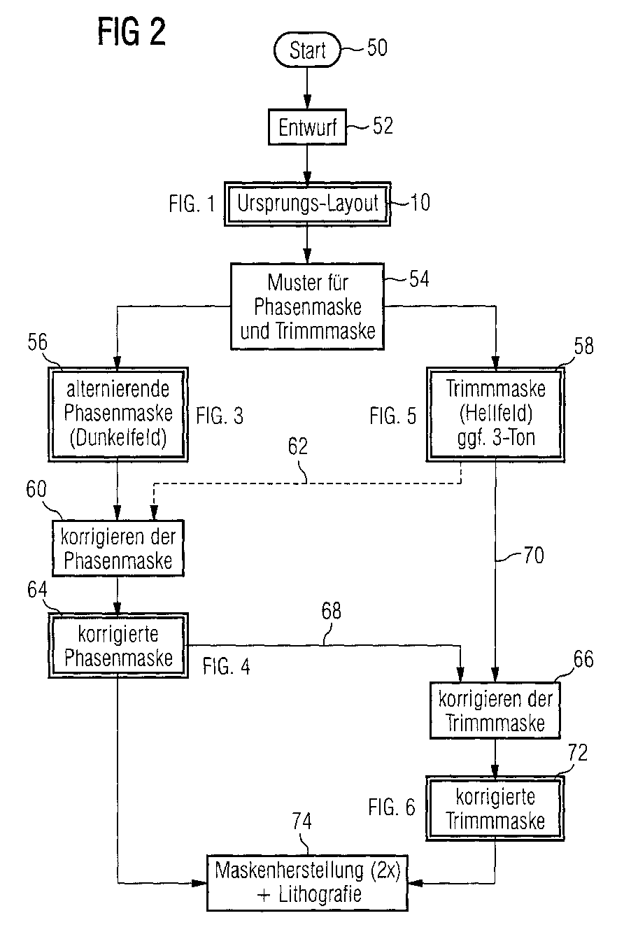
- Figure 2 shows process steps in the manufacture of a integrated circuit. The process begins in one Method step 50 with the specification of design requirements.
- a design department according to that specified in method step 50 Defined a draft.
- Result of the procedural step 52 is the original layout 10, see Figure 1.
- Figure 2 are layouts and patterns in contrast to process steps represented by a double frame.
- a method step following method step 52 54 starting from the original layout, 10 mask data for a phase shift mask and mask data for a trim mask generated.
- the process step 54 Design rules checked (design rule check). Also be Areas defined, their circuit structures with the phase shift mask should be generated. In the other areas the circuit structures with the help of the trim mask generated. With the help of the so-called staining method it is checked whether the passage areas of the phase shift mask are so arranged are that between neighboring transit areas a phase jump of 180 ° can be generated.
- the patterns 56 or 58 of an alternating phase jump mask or a trim mask in front are explained in more detail below with reference to FIG. 3.
- the pattern 58 of the trim mask is shown below with reference to FIG explained.
- process step 54 is in a process step 60 corrected the pattern 56 of the phase shift mask.
- goal of Correction is deviations between the original layout 10 and the geometric structure of the manufacture of the integrated circuit resulting circuit structure counteract. Line reductions, in particular, are said to be so and excessive corner rounding can be prevented.
- the procedural step 60 becomes the uncorrected pattern 58 of the trim mask not used in the simulation of the exposure process. Based on the simulation of the exposure process and the subsequent simulation of the manufacturing process of integrated circuit can be Line reductions, Corner rounding, structure width changes, structure width variations as well as an offset of structures. With the help of specified correction rules for the phase shift mask the deviations found are corrected. The result of the correction is a corrected pattern 64 the phase shift mask. The pattern is shown below using the figure 4 explained in more detail.
- the pattern 58 of the trim mask is corrected for aberrations to compensate for the exposure with the trim mask.
- the trim mask is used to correct pattern 58 trim mask pattern 58 and corrected pattern 64 the phase shift mask used, cf. Arrows 68 and 70.
- the pattern 58 of the Trim mask changed so that in particular line shortenings, Corner rounding, structure width changes, structure width variations and an offset of structures in the Manufacturing of the integrated circuit can be balanced.
- phase shift mask already corrected in method step 60 64 remains unchanged in method step 66.
- corrected phase shift mask 64 used to Simulation of the exposure process and to simulate the Manufacturing process.
- Result of the process step 66 is a corrected trim mask 72, the structure of which is below is explained in more detail with reference to Figure 6.
- Method step 66 is followed by method step 74, in which the phase shift mask based on the pattern data of the Pattern 64 and the trim mask based on the pattern data of the Pattern 72 can be produced with the aid of a mask pen.
- the integrated circuit is then manufactured. First, one with one becomes positive, for example working photoresist coated substrate in one Photo projection device exposed twice; once with the Phase jump mask and once with the trim mask. Subsequently the photoresist layer is developed, with the photoresist on the exposed areas is removed. Then in one wet chemical etching process the substrate at the exposed areas ablated.
- FIG. 3 shows the uncorrected pattern 56 for the phase shift mask.
- the phase shift mask is one in this case so-called dark field mask. This requires that in the pattern 56 outside of transit areas 100 to 110 and from Passage areas 120 to 136 lying areas impermeable to radiation are.
- the passage areas 100 to 110 as well the passage areas 120 to 134 are translucent Areas of the phase shift mask.
- the phase is compared to that by the Passage areas 100 to 110 light passing through Shifted 180 °, see 180 ° in Figure 3.
- the passage areas 100 to 110 and 120 to 134 alternate, see above that destructive interference between neighboring ones Passage areas 110 to 134 occurs.
- This destructive Interference enables the manufacturing of their dimensions critical structures because in the exposure between neighboring areas of darkness arise, in which the management structures later lie, e.g. between the passage areas 100 and 122 the upper right branch the line structure corresponding to line structure 16.
- the passage areas 120 to 134 are for differentiation of the passage areas 100 to 110 with one Dot grid covered.
- the passage areas 100 to 110 and 120 to 134 are in the Area of active areas 12 and 14, see Figure 1, because particularly high requirements in the active areas 12 and 14 to the dimensional accuracy of those to be produced with the aid of the pattern 56 Circuit structure can be put.
- the exact course of the Passage areas 100 to 134 were in method step 54 determined, see Figure 2.
- FIG. 4 shows the corrected pattern 64 for the corrected one Phase-shifting mask.
- the corrected phase shift mask is also a so-called dark field mask.
- Corrected pattern 64 contains passageways 140 to 150 in that order correspond to the passage areas 100 to 110. however are the passage areas 140 to 150 due to the in the process step 60 carried out correction in its outline more irregular than the corresponding passage areas 100 to 110.
- the passage areas 140 to 150 correspond in the corrected phase shift mask passage areas that generate a phase shift of 0 °.
- the pattern 64 contains also passage areas 160 to 174 that in this Sequence corresponds to the passage areas 120 to 134.
- the passage areas 160 to 174 are not as regular Outlines like the corresponding passage areas 120 to 134.
- the passage areas 160 to 174 correspond in the corrected phase shift mask passage areas that a Cause phase shift of 180 °.
- the transit areas too 140 to 150 alternate with the passage areas 160 to 174 to toggle between neighboring transit areas to generate a phase jump of 180 °.
- FIG. 182 and 184 depict the outline of the passage area 160 corresponding passage area 120, the outline of the passage area corresponding to passage area 140 100 and the outline of the area corresponding to the passage area 162 Show passage area 122. It's easy to see that the passage areas 160, 140 and 162 are longer are as the corresponding passage areas 120, 100 and 122. The extension should be the one that occurs during the exposure Line shortening can be counteracted. In the area the corners of the passage areas 160 to 174 are located mostly so-called serifs that counteract rounding of corners should, see e.g. Serifs 190 and 192.
- FIG. 5 shows the uncorrected pattern 58 of the trim mask.
- the Trim mask is a so-called bright field mask, in which the Light passes through the brightly drawn areas in FIG.
- Pattern 58 includes two masking areas 200 and 202.
- a covering area corresponding to the covering area 200 the trim mask would cover the areas during exposure, by exposure to the uncorrected phase shift mask in the area of the passage areas 100 to 104 and 120 to 126 would be exposed.
- the coverage area 200 is, for example, in the phase shift mask belonging to pattern 58 covered by a chrome layer covering the passage completely prevented by light.
- the covering area 202 corresponds to that belonging to the pattern 58 Phase shift mask an opaque area, that covers an area that is exposed when exposed to the phase shift mask would be exposed.
- the covering area is thus located 202 in pattern 58 at the positions where in Pattern 56, the passage areas 128 to 134 are located.
- Pattern 58 also includes outside of the coverage areas 200 and 202 line structures 206 through 214 used in this Order of the line structures 16 to 24 of the original layout see also Figure 1.
- the line structures 206 to 214 would be absorber structures in the uncorrected trim mask correspond to the incident light too absorb about 90 to 95%.
- the management structures 206 up to 214 corresponding absorber structures also lead a shift in the phase of the incident light. The phase shift is 180 ° compared to that through light passing through the surrounding areas.
- FIG. 6 shows the corrected pattern 72 of the trimming mask, which is generated from the uncorrected pattern 58 in method step 66.
- the corrected pattern 72 is used to produce a corrected trim mask, which is also a bright field mask.
- the pattern 72 includes an upper cover area 220 that emerged from the cover area 200.
- a lower covering area 222 has emerged from the covering area 202.
- the original positions of the covering areas 200 and 202 are illustrated in FIG. 6 by frames 224 and 226, respectively.
- the outline of the cover areas 220 and 222 is more irregular compared to the outline of the cover areas 200 and 202.
- both corrective measures serve to compensate for aberrations. Covering areas of the trim mask corresponding to the covering areas 220 and 222 are covered with a chrome layer and, for example, only have a transmission of 10 -6 .
- Pattern 72 also includes line structures 236 through 244, which in this order the line structures 206 to 214 of pattern 58 correspond.
- the course of the management structures 236 to 244 essentially agrees with the course line structures 206 through 214. However, they are Edges of the line structures 236 to 244 due to the im Method step 66, see FIG. 2, correction carried out more irregular than the edges of the line structures 206 to 214. For comparison, the original position of the Edges of line structures 206 through 214 by lines 250 shown.
- the line structures 236 to 244 protrude from some Pass beyond lines 250 and lie on others Digits within lines 250.
- Figure 7 shows the top view of an integrated circuit 260, its production with the help of a simulation program simulated using corrected patterns 64 and 72 has been.
- Line structures 266 to 274 show the covered with photoresist after developing the photoresist layer Areas.
- the line structures 266 to 274 correspond in their course the management structures 16 to 24, cf.
- Figure 7 shows that using the corrected Patterns 64 and 72 a circuit can be made whose management structures are only insignificant from the original layout 10 deviate.
- FIG. 8 shows an image 280 taken with a scanning electron microscope added to an integrated circuit made using masks which is due to uncorrected pattern 56 and 58 have been manufactured.
- the line structures 16 to 24 corresponding line structures of the one shown in FIG Circuit are surrounded by white outlines.
- Figure 8 are clearly bridges between the management structures as well considerable deviations can be seen in the outline.
- Figure 9 shows the result of the simulation of the manufacturing process of an integrated circuit 290. In the simulation were also uncorrected patterns 56 and 58 used. The simulation agrees very well with the recording 280 match. Conversely, it can be assumed that will also be corrected using the Circuit 64 and 72 manufactured by the Circuit 260 has structure shown.
- the line structures lying outside the active regions 12 and 14 are wider than the line structures 16 to 24 shown in FIG. 1.
- the line structures in the exemplary embodiment outside the regions 12 and 14 have one Larger distance from one another than the line structures 16 to 24 shown in FIG. 1. Because of the greater width and the greater distance, the production of the line structures lying outside the active regions 12 and 14 is then less critical than within the active regions 12 and 14. For this reason, instead of the absorber structures belonging to the line structures 206 to 214, there are absorber structures which absorb all the incident light.
- the absorber structures in the second exemplary embodiment have a transmission of 10 -6 because they are formed by a chrome layer.
Landscapes
- Physics & Mathematics (AREA)
- General Physics & Mathematics (AREA)
- Preparing Plates And Mask In Photomechanical Process (AREA)
- Exposure And Positioning Against Photoresist Photosensitive Materials (AREA)
- Networks Using Active Elements (AREA)
Abstract
Erläutert wird unter anderem ein Verfahren, bei dem zunächst
in einem ersten Korrekturschritt (60) das Muster (56) für die
Phasensprungmaske korrigiert wird. Anschließend wird in einem
zweiten Korrekturschritt (66) das Muster für die Trimmmaske
bei Einsatz des korrigierten Musters (64) für die Phasensprungmaske
korrigiert. Durch die beiden nacheinander ausgeführten
Korrekturschritte lassen sich Maskendaten für die
Herstellung höchstintegrierter Schaltkreise auf einfache Art
korrigieren.
Description
Die Erfindung betrifft ein Verfahren zum Erzeugen von korrigierten Mustern für eine Phasensprungsmaske und deren zugehöriger Trimmmaske. Bei dem Verfahren wird ein Ursprungs-Layout zur Herstellung einer Schaltungsstruktur mit Hilfe eines Photo-Lithografieverfahrens vorgegeben. Aus dem Ursprungs-Layout wird ein Muster für eine Phasensprungmaske erzeugt, mit deren Hilfe ein Teil der Schaltungsstruktur hergestellt werden soll. Außerdem wird aus dem Ursprungs-Layout ein Muster für eine Trimmmaske erzeugt, mit deren Hilfe sich an die Schaltungsstruktur des ersten Teils anschließende Strukturen der Schaltungsstruktur herstellbar sind und mit deren Hilfe Stellen belichtet werden, an denen direkte Phasenübergänge der Phasenmaske liegen. Das Muster für die Phasensprungmaske und das Muster für die Trimmmaske werden unter Berücksichtigung von Nachbarschaften der Strukturen der Muster mit Einfluss auf die Abbildung bei der Photolithografie so korrigiert, dass eine mit den korrigierten Mustern herstellbare Schaltungsstruktur hinsichtlich der Geometrie dem Ursprungs-Layout ähnlicher als eine mit den unkorrigierten Mustern herstellbare Schaltungsstruktur ist.The invention relates to a method for generating corrected Patterns for a phase shift mask and its associated one Trimming mask. The process uses an original layout for producing a circuit structure using a photo-lithography process specified. From the original layout a pattern for a phase shift mask is generated, with the Help part of the circuit structure be made should. The original layout also becomes a pattern for creates a trim mask, with the help of the circuit structure structures of the first part of the Circuit structure can be produced and with their help be exposed on which direct phase transitions of the Phase mask. The pattern for the phase shift mask and the pattern for the trim mask will be considered of neighborhoods of the structures of the patterns with influence corrected to the image in photolithography so that a circuit structure that can be produced with the corrected patterns in terms of geometry, the original layout more similar than one that can be produced with the uncorrected patterns Circuit structure is.
Ein solches Verfahren wird allgemein als OPC-Verfahren (optical proximity correction) bezeichnet, weil nachbarschaftsinduzierte Beugungseffekte korrigiert werden. Bei der Korrektur werden Nachbarschaften berücksichtigt die einen Einfluss auf die Abbildung bei der Photolithografie haben.Such a method is generally called OPC process (o ptical c p roximity orrection) because neighborhood induced diffraction effects are corrected. When correcting, neighborhoods are taken into account that have an influence on the image in photolithography.
Die Phasensprungmaske ist entweder eine Dunkelfeldmaske oder eine Hellfeldmaske. Beispielsweise enthält eine Phasensprungmaske vom Dunkelfeldtyp mindestens zwei Arten strahlungsdurchlässiger Gebiete mit voneinander unterschiedlichem Einfluss auf die Phase von durch die Durchtrittsgebiete übertragenen elektromagnetischen Wellen. Üblicherweise wird zwischen benachbarten Durchtrittsgebieten ein Phasensprung von 180° erzeugt.The phase shift mask is either a dark field mask or a bright field mask. For example, contains a phase shift mask of the dark field type at least two types of radiation transmissive Areas with different influences to the phase of transmitted through the passage areas electromagnetic waves. Usually between neighboring transition areas a phase jump of 180 ° generated.
Ein Verfahren mit den oben genannten Verfahrensschritten ist in dem Artikel "Integration of Optical Proximity Correction Strategies in Strong Phase Shifters Design for Poly-Gate Layers" von Christopher Spence, Marina Plat, Emile Sahouria, u.a., erläutert. Dieser Artikel ist Teil des 19th Annual BACUS Symposium on Photomask Technology, Monterey, California, September 1999 und in SPIE, Vol. 3873, Seiten 277 bis 287, veröffentlicht. Bei der Korrektur werden die Muster für die Phasensprungmaske und die Trimmmaske simultan korrigiert. In der Veröffentlichung werden Schaltungsstrukturen mit einer kritischen Dimension CD von 100 nm mit Hilfe von 248 nm Lithografie-Apparaten hergestellt. Zusätzlich wird der Herstellungsprozess simuliert. In der Veröffentlichung dargestellte Strukturen haben jedoch vergleichsweise große Abstände voneinander. Das Verhältnis von minimalem Abstand der Strukturen zu minimaler Strukturbreite ist wesentlich größer als zwei.A method with the above-mentioned method steps is explained in the article "Integration of Optical Proximity Correction Strategies in Strong Phase Shifters Design for Poly-Gate Layers" by Christopher Spence, Marina Plat, Emile Sahouria and others. This article is part of the 19 th Annual BACUS Symposium on Photomask Technology, Monterey, California, September 1999 and published in SPIE, Vol. 3873, pages 277 to 287. During the correction, the patterns for the phase shift mask and the trim mask are corrected simultaneously. In the publication, circuit structures with a critical dimension CD of 100 nm are produced with the help of 248 nm lithography apparatus. In addition, the manufacturing process is simulated. However, the structures shown in the publication are relatively far apart. The ratio of the minimum spacing of the structures to the minimum structure width is significantly greater than two.
Es ist Aufgabe der Erfindung, ein verbessertes OPC-Verfahren zum Korrigieren von Mustern für eine Phasensprungmaske und deren Trimmmaske anzugeben. Außerdem sollen eine zugehörige Vorrichtung, ein zugehöriges Programm, ein Datenträger mit diesem Programm sowie eine integrierte Schaltungsstruktur angegeben werden.It is an object of the invention to provide an improved OPC method for correcting patterns for a phase shift mask and specify their trim mask. In addition, an associated Device, an associated program, a disk with this program and an integrated circuit structure become.
Die das Verfahren betreffende Aufgabe wird durch die im Patentanspruch 1 angegebenen Verfahrensschritte gelöst. Weiterbildungen sind in den Unteransprüchen angegeben.The task relating to the method is achieved by the in claim 1 specified process steps solved. further developments are specified in the subclaims.
Die Erfindung geht von der Überlegung aus, dass Phasensprungmasken üblicherweise zum Herstellen von Schaltungsstrukturen eingesetzt werden, deren kritische Dimension so klein ist, dass bei der Abbildung der Strukturen mit Hilfe der Masken Nachbarschaften der Strukturen die Abbildung beeinflussen. Eine gleichzeitige Korrektur des Musters der Phasensprungmaske und des Musters der Trimmmaske ist zwar möglich, jedoch mit einem vergleichsweise großen Aufwand verbunden, weil sich der Einfluss der Nachbarschaften auf die Abbildung bei der Photolithografie nur schwer abschätzen lässt.The invention is based on the consideration that phase shift masks usually for the production of circuit structures whose critical dimension is so small that when mapping structures using masks Neighborhoods of the structures that influence the image. A simultaneous correction of the pattern of the phase shift mask and the pattern of the trim mask is possible, however associated with a comparatively large effort because the influence of the neighborhoods on the mapping at the Difficult to estimate photolithography.
Beim erfindungsgemäßen Verfahren wird zusätzlich zu den eingangs genannten Verfahrensschritten zunächst in einem ersten Korrekturschritt das Muster für die Phasensprungmaske nach Korrekturvorschriften für das Muster der Phasensprungmaske korrigiert. Anschließend wird dann in einem zweiten Korrekturschritt das Muster für die Trimmmaske bei Einsatz des korrigierten Musters für die Phasensprungmaske nach Korrekturvorschriften für das Muster der Trimmmaske korrigiert. Durch die Trennung der Korrektur des Musters für die Phasensprungmaske von der Korrektur des Musters für die Trimmmaske wird erreicht, dass während des Korrekturverfahrens nicht so viele verschiedene Einflüsse gleichzeitig berücksichtigt werden müssen. Somit ist der Einfluss der Nachbarschaften auf die Abbildung bei der Photolithografie besser beherrschbar. Insgesamt ist der Aufwand für die Korrektur beim erfindungsgemäßen Verfahren erheblich geringer als bei gleichzeitiger Korrektur beider Muster.In the method according to the invention, in addition to the above mentioned process steps first in a first Correction step after the pattern for the phase shift mask Correction rules for the pattern of the phase shift mask corrected. Then in a second correction step the pattern for the trim mask when using the corrected Patterns for the phase shift mask according to correction instructions corrected for the pattern of the trim mask. By the separation of the correction of the pattern for the phase shift mask from correcting the pattern for the trim mask achieved that not so many during the correction process different influences are taken into account at the same time have to. So the influence of the neighborhoods on the Image more controllable in photolithography. All in all is the effort for the correction in the invention Procedure considerably less than with simultaneous correction both patterns.
Bei einer Alternative des erfindungsgemäßen Verfahrens wird zunächst in einem ersten Korrekturschritt das Muster für die Trimmmaske nach Korrekturvorschriften für das Muster der Trimmmaske korrigiert. Anschließend wird dann in einem zweiten Korrekturschritt das Muster für die Phasensprungmaske bei Einsatz des korrigierten Musters für die Trimmmaske nach Korrekturvorschriften für das Muster der Phasensprungmaske korrigiert. Somit ist die Reihenfolge der Korrekturschritte wählbar. Die Reihenfolge wird so festgelegt, dass möglichst einfache Korrekturvorschriften aufgestellt werden können. In an alternative of the method according to the invention first in a first correction step the pattern for the Trim mask according to correction instructions for the pattern of the Trim mask corrected. Then in a second Correction step the pattern for the phase shift mask Use of the corrected pattern for the trim mask according to correction instructions corrected for the pattern of the phase shift mask. So the order of the correction steps is selectable. The order is determined so that if possible simple correction instructions can be drawn up.
Bei einer Weiterbildung wird im ersten Korrekturschritt das Muster für die Phasensprungmaske bei Einsatz des unkorrigierten Musters für die Trimmmaske korrigiert. Alternativ wird im ersten Korrekturschritt das Muster für die Trimmmaske bei Einsatz des unkorrigierten Musters für die Phasensprungmaske korrigiert. Durch diese Maßnahmen lassen sich genauere Korrekturvorschriften ermitteln.In the case of further training, this is the first correction step Pattern for the phase shift mask when using the uncorrected Corrected pattern for the trim mask. Alternatively, in first correction step the pattern for the trim mask Use of the uncorrected pattern for the phase shift mask corrected. These measures allow more precise correction instructions determine.
Im ersten Korrekturschritt werden vorzugsweise im wesentlichen alle bzw. alle Korrekturen durchgeführt, die sich nach den vorgegebenen Korrekturvorschriften für die erste korrigierte Maske an deren Muster ausführen lassen. Im zweiten Korrekturschritt werden dann im wesentlichen alle bzw. alle Korrekturen ausgeführt, die sich zum Zeitpunkt der Ausführung des Verfahrens nach den für die zweite zu korrigierende Maske vorgegebenen Korrekturvorschriften an dem Muster der als zweite Maske korrigierten Maske ausführen lassen. Im wesentlichen alle bedeutet, dass beispielsweise einzelne Korrekturen später noch manuell im Sinne einer Nachbesserung ausgeführt werden können. Es werden also Korrekturen an allen Stellen des Musters ausgeführt, an denen Korrekturen gemäß der Korrekturvorschriften ausführbar sind. Die Korrekturschritte sind so klar voneinander getrennt.In the first correction step, preferably essentially all or all corrections carried out after the prescribed correction rules for the first corrected Have the mask run on their pattern. In the second Correction steps are then essentially all or all Corrections carried out at the time of execution the method according to the mask to be corrected for the second given correction instructions on the pattern of as second mask have the mask corrected. Essentially all means, for example, individual corrections later carried out manually as a touch-up can be. So there will be corrections to everyone Locations of the pattern carried out on which corrections according the correction instructions are executable. The correction steps are so clearly separated.
Beispielsweise werden aufgrund der Korrekturvorschriften:
- Linienverkürzungen bei der Herstellung der Schaltungsstruktur im Vergleich zum Muster bzw. Ursprungs-Layout durch Verlängerung der betreffenden Struktur in einem der beiden Muster beseitigt,
- Abrundungen von Ecken in der hergestellten Schaltungsstruktur bzw. bei der Simulation der Herstellung auftretende Abrundungen von Ecken durch "Anstückeln" von Korrekturflächen in einem der beiden Muster vermieden, und
- Einengungen bei der hergestellten bzw. simulierten Schaltungsstruktur vermieden, indem die diese Schaltungsstrukturen hervorrufende Strukturen in einem der beiden Muster in den Bereichen der Einengung verbreitert werden.
- Line shortening in the manufacture of the circuit structure in comparison to the pattern or original layout has been eliminated by extending the structure in question in one of the two patterns,
- Rounding of corners in the circuit structure produced, or rounding of corners occurring in the simulation of the production, by “patching” correction surfaces in one of the two patterns, and
- Constrictions in the manufactured or simulated circuit structure are avoided by broadening the structures causing these circuit structures in one of the two patterns in the areas of the constriction.
Bei einer nächsten Weiterbildung des Verfahrens ist die Korrektur nach Ausführung des zweiten Korrekturschritts im wesentlichen beendet, d.h. beispielsweise abgesehen von geringen manuellen Nachbesserungen.The next time the method is developed is the correction after performing the second correction step essentially ended, i.e. for example apart from minor manual rework.
Die mit Hilfe des erfindungsgemäßen Verfahrens bzw. mit Hilfe von dessen Weiterbildungen erzeugten Muster werden als Grundlage bei der Herstellung oder der Simulation der Herstellung einer Phasensprungmaske und einer Trimmmaske eingesetzt. Beispielsweise werden Maskendaten erzeugt, die direkt in einen Maskenschreiber eingegeben werden können. Wird dagegen der Herstellungsprozess simuliert, so lassen sich Masken für Schaltungsstrukturen entwickeln, die erst in ein oder zwei Jahren hergestellt werden, weil die zur Herstellung benötigten Vorrichtungen noch entwickelt werden. Aufgrund der Simulation der Herstellung der Schaltung lassen sich sehr früh Fehler im Muster erkennen und korrigieren. In diesem Fall wird das erfindungsgemäße Verfahren bzw. seine Weiterbildungen mehrmals ausgeführt, wobei anstelle des Ursprungs-Layouts ein neues Ursprungslayout verwendet wird. Alternativ oder zusätzlich lassen sich auch Veränderungen am ursprünglichen Muster für die Phasensprungmaske und/oder am Muster für die Trimmmaske vornehmen.That with the help of the method according to the invention or with the help patterns created by its further training are the basis in manufacturing or simulating manufacturing a phase shift mask and a trim mask. For example mask data is generated, which is directly in a Mask writers can be entered. However, if the Manufacturing process simulated, so masks for Develop circuit structures that only come in one or two Years ago, because the ones needed to manufacture them Devices are still being developed. Because of the simulation the manufacture of the circuit can be started very early Detect and correct errors in the pattern. In this case is the inventive method and its developments executed several times, instead of the original layout a new original layout is used. Alternatively or additionally you can also make changes to the original Pattern for the phase shift mask and / or on the pattern for the Make trim mask.
Bei einer nächsten Weiterbildung sind die Muster durch Masken-Daten festgelegt. Das Verfahren wird mit Hilfe mindestens einer Datenverarbeitungsanlage ausgeführt. Bei einer Ausgestaltung erfolgt die Korrektur automatisch. Die Weiterbildung und die Ausgestaltung werden insbesondere zur Vorbereitung der Herstellung von höchstintegrierten Schaltungsstrukturen eingesetzt, z.B. von Mikroprozessoren oder Speicherbausteinen. Die Korrektur von mehreren Millionen Teilstrukturen der Muster lässt sich so auf einfache Weise und mit vertretbarem Aufwand durchführen. In a next development, the patterns are through mask data established. The procedure is at least with the help executed a data processing system. In one configuration the correction takes place automatically. Continuing education and the design will be especially in preparation the manufacture of highly integrated circuit structures used, e.g. microprocessors or memory chips. The correction of several million substructures of the Pattern can be easily and with reasonable Carry out effort.
Die Erfindung betrifft außerdem eine Vorrichtung zum Korrigieren von Mustern für eine Phasensprungmaske und deren Trimmmaske, insbesondere eine Datenverarbeitungsanlage. Die Vorrichtung enthält eine Speichereinheit zum Speichern der Daten des Ursprungs-Layouts, der Daten des Musters für die Phasensprungmaske und der Daten des Musters für die Trimmmaske. Eine Korrektureinheit führt die Korrektur des Musters der Phasensprungmaske und die Korrektur des Musters der Trimmmaske durch. Dabei werden nacheinander die beiden oben erwähnten Korrekturschritte ausgeführt. Somit gelten die oben im Zusammenhang mit dem erfindungsgemäßen Verfahren genannten technischen Wirkungen auch für die erfindungsgemäße Vorrichtung.The invention also relates to a device for correction of patterns for a phase shift mask and its Trim mask, in particular a data processing system. The Device contains a storage unit for storing the Data of the original layout, the data of the pattern for the Phase jump mask and the data of the pattern for the trim mask. A correction unit carries out the correction of the pattern of the Phase jump mask and the correction of the pattern of the trim mask by. The two above are mentioned one after the other Correction steps carried out. So the above applies in context technical with the inventive method Effects also for the device according to the invention.
Bei Weiterbildungen ist die Vorrichtung so aufgebaut, dass sie im Betrieb ein Verfahren nach einer Weiterbildung des erfindungsgemäßen Verfahrens ausführt. Beispielsweise wird die Korrektur automatisch ausgeführt.In the case of further developments, the device is constructed such that they operate a method according to a development of the invention Procedure. For example, the Correction carried out automatically.
Die Erfindung betrifft außerdem ein Programm zum Korrigiere von Mustern für eine Phasensprungmaske und deren Trimmmaske. Beim Ausführen der Befehle des Programms durch einen Prozessor werden die Korrekturschritte des erfindungsgemäßen Verfahrens ausgeführt. Somit gelten die oben genannten technischen Wirkungen auch für das Programm.The invention also relates to a program for correcting of patterns for a phase shift mask and its trim mask. When the instructions of the program are executed by a processor are the correction steps of the method according to the invention executed. Thus, the above technical ones apply Effects also for the program.
Bei einer Weiterbildung ist ein Teil der Befehle des Programms in einer Datei enthalten, die Befehle einer Kommandosprache zur Steuerung des Programmablaufs enthält. Durch den Einsatz sogenannter Script-Dateien lassen sich Programme zur Ausführung des erfindungsgemäßen Verfahrens einsetzen, die zwar zur Durchführung des Verfahrens grundsätzlich geeignet sind, bei denen die Inhalte der Script-Datei jedoch noch nicht in den Quell-Code übernommen worden sind. Dies kann zu einem späteren Zeitpunkt erfolgen. Ein Programm, das zur Ausführung des Verfahrens mit Hilfe einer Script-Datei geeignet ist, ist beispielsweise das Programm "Optissimo" der Firma aiss GmbH, München, Deutschland, in der Version des Jahres 2000.In the case of further training, part of the commands of the program contained in a file, the commands of a command language for controlling the program flow contains. By the Programs can be used for so-called script files Use execution of the method according to the invention basically suitable for carrying out the method where the content of the script file is still have not been included in the source code. This can be too at a later date. A program to run the procedure with the help of a script file is, for example, the company's "Optissimo" program aiss GmbH, Munich, Germany, in the version of the year 2000th
Bei einer nächsten Weiterbildung des erfindungsgemäßen Programms ist das Programm so aufgebaut, dass bei der Ausführung seiner Befehle ein Verfahren nach einer der oben genannten Weiterbildungen der Erfindung ausgeführt wird. Die oben genannten technischen Wirkungen gelten demzufolge auch für die Weiterbildungen des Programms.In a next development of the program according to the invention the program is structured so that when it is executed his commands a procedure according to one of the above Developments of the invention is carried out. The above technical effects therefore also apply to Further training of the program.
Mit der Erfindung bzw. ihren Weiterbildungen lassen sich integrierte
Schaltungsstrukturen herstellen, für deren minimale
kritische Dimension gilt:
Durch die Erfindung betroffen sind auch Schaltungsstrukturen, die unter Verwendung von Masken hergestellt werden, deren Muster gemäß dem erfindungsgemäßen Verfahren vorgegeben werden. Weiterhin sind eine Phasensprungmaske und eine Trimmmaske geschützt, die mit Hilfe des erfindungsgemäßen Verfahrens oder einer seiner Weiterbildungen hergestellt worden sind. Circuit structures are also affected by the invention, made using masks whose Patterns can be specified according to the inventive method. There are also a phase shift mask and a trim mask protected using the method according to the invention or one of its training courses have been produced.
Im folgenden werden Ausführungsbeispiele der Erfindung an Hand der beiliegenden Zeichnungen erläutert. Darin zeigen:
- Figur 1
- ein Ursprungs-Layout mit zwei aktiven Bereichen,
- Figur 2
- Verfahrensschritte bei der Herstellung eines integrierten Schaltkreises,
Figur 3- ein unkorrigiertes Muster für eine Phasensprungmaske,
- Figur 4
- ein korrigiertes Muster für eine korrigierte Phasensprungmaske,
- Figur 5
- ein unkorrigiertes Muster für eine Trimmmaske,
- Figur 6
- ein korrigiertes Muster für eine korrigierte Trimmmaske,
- Figur 7
- das Ergebnis der Simulation des Herstellungsprozesses des integrierten Schaltkreises unter Verwendung der korrigierten Muster,
- Figur 8
- eine mit Hilfe eines Raster-Elektronen-Mikroskops erstellte Aufnahme eines unter Verwendung der unkorrigierten Muster hergestellten integrierten Schaltkreises, und
- Figur 9
- das Ergebnis der Simulation des Herstellungsprozesses des integrierten Schaltkreises unter Verwendung der unkorrigierten Muster.
- Figure 1
- an original layout with two active areas,
- Figure 2
- Process steps in the manufacture of an integrated circuit,
- Figure 3
- an uncorrected pattern for a phase shift mask,
- Figure 4
- a corrected pattern for a corrected phase shift mask,
- Figure 5
- an uncorrected pattern for a trim mask,
- Figure 6
- a corrected pattern for a corrected trim mask,
- Figure 7
- the result of the simulation of the manufacturing process of the integrated circuit using the corrected pattern,
- Figure 8
- a scanning electron micrograph of an integrated circuit made using the uncorrected patterns, and
- Figure 9
- the result of the simulation of the manufacturing process of the integrated circuit using the uncorrected patterns.
Figur 1 zeigt ein Ursprungs-Layout 10 mit zwei aktiven Bereichen
12 und 14. Eine unter der mit Hilfe des Ursprungs-Layouts
10 herzustellenden Schicht liegende Schicht wird unterhalb
des den aktiven Bereichen 12 und 14 entsprechenden
Bereiches beispielsweise p-dotiert. Das Ursprungs-Layout 10
enthält außerdem fünf Leitungsstrukturen 16 bis 24. Den Leitungsstrukturen
16 bis 24 entsprechen Leitungsstrukturen im
herzustellenden integrierten Schaltkreis. Entsprechend bedeutet
hierbei, dass die Schaltungsstrukturen bezüglich eines
vorgegebenen Bezugspunktes in der Schaltungsstruktur an derselben
Stelle liegen wie die entsprechende Leitungsstruktur
im Ursprungs-Layout 10. Innerhalb der den aktiven Bereichen
12 und 14 entsprechenden Bereichen werden die den Leitungsstrukturen
16 bis 24 entsprechenden Schaltungsstrukturen n-dotiert,
und bilden so die Steueranschlüsse (Gate) von Transistoren.
Außerhalb der aktiven Bereiche 12 und 14 sind die
den Leitungsstrukturen 16 bis 24 entsprechenden Leitungsstrukturen
gute elektrische Leiter und haben die Funktion von
Verbindungsleitungen. Jede Leiterstruktur 16 bis 24 hat außerdem
eine Anschlussfläche 26, 28, 30, 32 bzw. 34. Den Anschlussflächen
26 bis 34 entsprechende Anschlussflächen in
der Schaltungsstruktur dienen zum Zuführen bzw. Abnehmen von
elektrischen Signalen.FIG. 1 shows an
Eine Maßstabsstrecke 36 hat die Länge von 1 cm und entspricht
100 nm der späteren Schaltungsstruktur. Zur Herstellung der
Schaltungsstruktur wird bei der Belichtung der Masken Licht
mit einer Wellenlänge von 248 nm eingesetzt. Die numerische
Apertur der Belichtungseinheit beträgt 0,63.A
Figur 2 zeigt Verfahrensschritte bei der Herstellung eines
integrierten Schaltkreises. Das Verfahren beginnt in einem
Verfahrensschritt 50 mit der Vorgabe von Entwurfsanforderungen.Figure 2 shows process steps in the manufacture of a
integrated circuit. The process begins in one
In einem folgenden Verfahrensschritt 52 wird durch eine Design-Abteilung
gemäß der im Verfahrensschritt 50 vorgegebenen
Vorgaben ein Entwurf erarbeitet. Ergebnis des Verfahrensschritts
52 ist das Ursprungs-Layout 10, siehe Figur 1. In
Figur 2 sind Layouts und Muster im Gegensatz zu Verfahrensschritten
durch einen doppelten Rahmen dargestellt. In a
In einem dem Verfahrensschritt 52 folgenden Verfahrensschritt
54 werden ausgehend vom Ursprungs-Layout 10 Masken-Daten für
eine Phasensprungmaske und Masken-Daten für eine Trimmmaske
erzeugt. Unter anderem werden im Verfahrensschritt 54 die
Entwurfsregeln geprüft (Design-Rule-Check). Außerdem werden
Bereiche festgelegt, deren Schaltungsstrukturen mit der Phasensprungmaske
erzeugt werden sollen. In den anderen Bereichen
werden die Schaltungsstrukturen mit Hilfe der Trimmmaske
erzeugt. Mit Hilfe der sogenannten Färbungsmethode wird geprüft,
ob die Durchtrittsgebiete der Phasensprungmaske so angeordnet
sind, dass zwischen jeweils benachbarten Durchtrittsgebieten
ein Phasensprung von 180° erzeugt werden kann.In a method step following
Am Ende des Verfahrensschritts 54 liegen die Muster 56 bzw.
58 einer alternierenden Phasensprungmaske bzw. einer Trimmmaske
vor. Die geometrische Struktur, d.h. das Muster 56 der
Phasensprungmaske wird unten an Hand der Figur 3 näher erläutert.
An Hand der Figur 5 wird unten das Muster 58 der Trimmmaske
erläutert.At the end of
Nach dem Verfahrensschritt 54 wird in einem Verfahrensschritt
60 das Muster 56 der Phasensprungmaske korrigiert. Ziel der
Korrektur ist es, Abweichungen zwischen dem Ursprungs-Layout
10 und der geometrischen Struktur der bei der Herstellung des
integrierten Schaltkreises entstehenden Schaltungsstruktur
entgegenzuwirken. So sollen insbesondere Linienverkürzungen
und zu starke Eckenabrundungen verhindert werden. Im Verfahrensschritt
60 wird das unkorrigierte Muster 58 der Trimmmaske
nicht bei der Nachbildung des Belichtungsprozesses eingesetzt.
An Hand der Nachbildung des Belichtungsprozesses und
der anschließenden Simulation des Herstellungsprozesses der
integrierten Schaltung lassen sich u.a. Linienverkürzungen,
Eckenabrundungen, Strukturbreitenveränderungen, Strukturbreitenvariationen
sowie ein Versatz von Strukturen feststellen.
Mit Hilfe vorgegebener Korrekturvorschriften für die Phasensprungmaske
werden die festgestellten Abweichungen korrigiert.
Ergebnis der Korrektur ist ein korrigiertes Muster 64
der Phasensprungmaske. Das Muster wird unten an Hand der Figur
4 näher erläutert.After
In einem dem Verfahrensschritt 60 folgenden Verfahrensschritt
66 wird das Muster 58 der Trimmmaske korrigiert, um Abbildungsfehler
bei der Belichtung mit der Trimmmaske auszugleichen.
Für die Korrektur des Musters 58 der Trimmmaske wird
das Muster 58 der Trimmmaske und das korrigierte Muster 64
der Phasensprungmaske eingesetzt, vgl. Pfeile 68 und 70. Bei
der Korrektur im Verfahrensschritt 66 wird das Muster 58 der
Trimmmaske so verändert, dass insbesondere Linienverkürzungen,
Eckenabrundungen, Strukturbreitenveränderungen, Strukturbreitenvariationen
und ein Versatz von Strukturen bei der
Herstellung des integrierten Schaltkreises ausgeglichen werden.In a method step following
Die bereits im Verfahrensschritt 60 korrigierte Phasensprungmaske
64 bleibt im Verfahrensschritt 66 unverändert. Zur
Nachbildung des Belichtungsprozesses und zur Simulation des
Herstellungsverfahrens wird also die korrigierte Phasensprungmaske
64 eingesetzt. Ergebnis des Verfahrensschrittes
66 ist eine korrigierte Trimmmaske 72, deren Struktur unten
an Hand der Figur 6 näher erläutert wird.The phase shift mask already corrected in
Dem Verfahrensschritt 66 folgt ein Verfahrensschritt 74, in
welchem die Phasensprungmaske aufgrund der Muster-Daten des
Musters 64 und die Trimmmaske aufgrund der Muster-Daten des
Musters 72 mit Hilfe eines Maskenschreibers hergestellt werden.
Anschließend wird der integrierte Schaltkreis hergestellt.
Dabei wird zunächst ein mit einem beispielsweise positiv
arbeitenden Fotoresist beschichtetes Substrat in einer
Photoprojektionsvorrichtung zweimal belichtet; einmal mit der
Phasensprungmaske und einmal mit der Trimmmaske. Anschließend
wird die Fotoresistschicht entwickelt, wobei der Fotolack an
den belichteten Stellen entfernt wird. Danach wird in einem
naßchemischen Ätzprozess das Substrat an den freigelegten Bereichen
abgetragen.
Figur 3 zeigt das unkorrigierte Muster 56 für die Phasensprungmaske.
Die Phasensprungmaske ist in diesem Fall eine
sogenannte Dunkelfeldmaske. Dies erfordert, dass die im Muster
56 außerhalb von Durchtrittsgebieten 100 bis 110 und von
Durchtrittsgebieten 120 bis 136 liegenden Bereiche strahlungsundurchlässig
sind. Die Durchtrittsgebiete 100 bis 110 sowie
die Durchtrittsgebiete 120 bis 134 stellen dagegen lichtdurchlässige
Gebiete der Phasensprungmaske dar. Jedoch unterscheidet
sich die Dicke der Phasensprungmaske innerhalb der
Durchtrittsgebiete 100 bis 110 im Vergleich zu den Durchtrittsgebieten
120 bis 134. Der Dickenunterschied ist so bemessen,
dass die Phase des auf die Phasensprungmaske auftreffenden
Lichtes in den Durchtrittsgebieten 100 bis 110 nicht
geändert wird, d.h. es tritt keine Phasenverschiebung in den
Durchtrittsgebieten 100 bis 110 auf, siehe 0° in Figur 3.
Beim Durchtritt des Lichtes durch die Durchtrittsgebiete 120
bis 134 wird dagegen die Phase im Vergleich zu dem durch die
Durchtrittsgebiete 100 bis 110 hindurchtretenden Licht um
180° verschoben, siehe 180° in Figur 3. Die Durchtrittsgebiete
100 bis 110 sowie 120 bis 134 wechseln einander ab, so
dass eine destruktive Interferenz zwischen benachbarten
Durchtrittsgebieten 110 bis 134 auftritt. Diese destruktive
Interferenz ermöglicht das Herstellen von in ihren Abmessungen
kritischen Strukturen, weil bei der Belichtung zwischen
benachbarten Durchtrittsgebieten dunkle Bereiche entstehen,
in denen später die Leitungsstrukturen liegen, z.B. zwischen
den Durchtrittsgebieten 100 und 122 der rechte obere Zweig
der der Leitungsstruktur 16 entsprechenden Leitungsstruktur.
In Figur 3 sind die Durchtrittsgebiete 120 bis 134 zur Unterscheidung
von den Durchtrittsgebieten 100 bis 110 mit einem
Punktraster bedeckt.FIG. 3 shows the
Die Durchtrittsgebiete 100 bis 110 und 120 bis 134 liegen im
Bereich der aktiven Bereiche 12 und 14, siehe Figur 1, weil
in den aktiven Bereichen 12 und 14 besonders hohe Anforderungen
an die Maßhaltigkeit der mit Hilfe des Musters 56 herzustellenden
Schaltungsstruktur gestellt werden. Die Durchtrittsgebiete
100 bis 134 ragen zum großen Teil über die aktiven
Bereiche 12 und 14 hinaus. Der genaue Verlauf der
Durchtrittsgebiete 100 bis 134 wurde im Verfahrensschritt 54
ermittelt, siehe Figur 2.The
Figur 4 zeigt das korrigierte Muster 64 für die korrigierte
Phasensprungmaske. Auch die korrigierte Phasensprungmaske ist
eine sogenannte Dunkelfeldmaske. Das korrigierte Muster 64
enthält Durchtrittsgebiete 140 bis 150, die in dieser Reihenfolge
den Durchtrittsgebieten 100 bis 110 entsprechen. Jedoch
sind die Durchtrittsgebiete 140 bis 150 aufgrund der im Verfahrensschritt
60 durchgeführten Korrektur in ihrem Umriss
unregelmäßiger als die entsprechenden Durchtrittsgebiete 100
bis 110. Den Durchtrittsgebieten 140 bis 150 entsprechen in
der korrigierten Phasensprungmaske Durchtrittsgebiete, die
eine Phasenverschiebung von 0° erzeugen. Das Muster 64 enthält
außerdem Durchtrittsgebiete 160 bis 174, die in dieser
Reihenfolge den Durchtrittsgebieten 120 bis 134 entsprechen.
Die Durchtrittsgebiete 160 bis 174 haben nicht so regelmäßige
Umrisse wie die entsprechenden Durchtrittsgebiete 120 bis
134. Den Durchtrittsgebieten 160 bis 174 entsprechen in der
korrigierten Phasensprungmaske Durchtrittsgebiete, die eine
Phasenverschiebung von 180° verursachen. Auch die Durchtrittsgebiete
140 bis 150 wechseln sich mit den Durchtrittsgebieten
160 bis 174 ab, um zwischen benachbarten Durchtrittsgebieten
einen Phasensprung von 180° zu erzeugen.FIG. 4 shows the corrected
Zum Vergleich der Umrisse sind in Figur 4 drei Rahmen 180,
182 und 184 dargestellt, die den Umriss des dem Durchtrittsgebiet
160 entsprechenden Durchtrittsgebiets 120, den Umriss
des im Durchtrittsgebiet 140 entsprechenden Durchtrittsgebiets
100 sowie den Umriss des dem Durchtrittsgebiet 162 entsprechenden
Durchtrittsgebiets 122 zeigen. Es ist gut zu erkennen,
dass die Durchtrittsgebiete 160, 140 und 162 länger
sind als die entsprechenden Durchtrittsgebiete 120, 100 und
122. Durch die Verlängerung soll der bei der Belichtung auftretenden
Linienverkürzung entgegengewirkt werden. Im Bereich
der Ecken der Durchtrittsgebiete 160 bis 174 befinden sich
meist sogenannte Serifen, die einer Eckenabrundung entgegenwirken
sollen, siehe z.B. Serifen 190 und 192.To compare the outlines, three
Figur 5 zeigt das unkorrigierte Muster 58 der Trimmmaske. Die
Trimmmaske ist eine sogenannte Hellfeldmaske, bei der das
Licht durch die in Figur 5 hell gezeichneten Flächen hindurchtritt.
Das Muster 58 enthält zwei Abdeckbereiche 200 und
202. Ein dem Abdeckbereich 200 entsprechender Abdeckbereich
der Trimmmaske würde bei der Belichtung die Bereiche überdecken,
die durch Belichtung mit der unkorrigierten Phasensprungmaske
im Bereich der Durchtrittsgebiete 100 bis 104 und
120 bis 126 belichtet werden würden. Der Abdeckbereich 200
ist bei der zum Muster 58 gehörenden Phasensprungmaske beispielsweise
durch eine Chromschicht bedeckt, die den Durchtritt
von Licht vollständig verhindert.FIG. 5 shows the
Dem Abdeckbereich 202 entspricht in der zum Muster 58 gehörenden
Phasensprungmaske ein lichtundurchlässiger Bereich,
der ein Gebiet überdeckt, das bei der Belichtung mit der Phasensprungmaske
belichtet werden würde. Somit liegt der Abdeckbereich
202 im Muster 58 an den Positionen, an denen im
Muster 56 die Durchtrittsbereiche 128 bis 134 liegen.The
Das Muster 58 enthält außerdem außerhalb der Abdeckbereiche
200 und 202 Leitungsstrukturen 206 bis 214, die in dieser
Reihenfolge den Leitungsstrukturen 16 bis 24 des Ursprungs-Layouts
entsprechen, siehe auch Figur 1. Den Leitungsstrukturen
206 bis 214 würden in der unkorrigierten Trimmmaske Absorberstrukturen
entsprechen, die das auftreffende Licht zu
etwa 90 bis 95 % absorbieren. Die den Leitungsstrukturen 206
bis 214 entsprechenden Absorberstrukturen führen ebenfalls
eine Verschiebung der Phase des auftreffenden Lichtes aus.
Die Phasenverschiebung beträgt 180° im Vergleich zu dem durch
die umliegenden Gebiete hindurchtretenden Licht.
Figur 6 zeigt das korrigierte Muster 72 der Trimmmaske, das
im Verfahrensschritt 66 aus dem unkorrigierten Muster 58 erzeugt
wird. Das korrigierte Muster 72 dient zur Herstellung
einer korrigierten Trimmmaske, die ebenfalls eine Hellfeldmaske
ist. Das Muster 72 enthält einen oberen Abdeckbereich
220, der aus dem Abdeckbereich 200 hervorgegangen ist. Ein
unterer Abdeckbereich 222 ist aus dem Abdeckbereich 202 hervorgegangen.
Zum Vergleich sind in Figur 6 die ursprünglichen
Positionen der Abdeckbereiche 200 und 202 durch Rahmen 224
bzw. 226 verdeutlicht. Der Umriss der Abdeckbereiche 220 und
222 ist im Vergleich zum Umriss der Abdeckbereiche 200 und
202 unregelmäßiger. Es gibt in den Abdeckbereichen 220 und
222 sowohl Gebiete, die über die Rahmen 224 bzw. 226 hinausragen,
als auch Gebiete, die innerhalb der Rahmen 224 bzw.
226 enden. Beide Korrekturmaßnahmen dienen jedoch dazu, Abbildungsfehler
auszugleichen. Den Abdeckbereichen 220 und 222
entsprechende Abdeckbereiche der Trimmmaske werden mit einer
Chromschicht überzogen und haben beispielsweise nur noch eine
Transmission von 10-6.FIG. 6 shows the corrected
Das Muster 72 enthält außerdem Leitungsstrukturen 236 bis
244, die in dieser Reihenfolge den Leitungsstrukturen 206 bis
214 des Musters 58 entsprechen. Der Verlauf der Leitungsstrukturen
236 bis 244 stimmt im wesentlichen mit dem Verlauf
der Leitungsstrukturen 206 bis 214 überein. Jedoch sind die
Ränder der Leitungsstrukturen 236 bis 244 aufgrund der im
Verfahrensschritt 66, siehe Figur 2, ausgeführten Korrektur
unregelmäßiger als die Ränder der Leitungsstrukturen 206 bis
214. Zum Vergleich ist in Figur 6 die ursprüngliche Lage der
Ränder der Leitungsstrukturen 206 bis 214 durch Linien 250
dargestellt. Die Leitungsstrukturen 236 bis 244 ragen an einigen
Stellen über die Linien 250 hinaus und liegen an anderen
Stellen innerhalb der Linien 250.
Figur 7 zeigt die Draufsicht auf einen integrierten Schaltkreis
260, dessen Herstellung mit Hilfe eines Simulationsprogramms
unter Verwendung der korrigierten Muster 64 und 72 simuliert
worden ist. Leitungsstrukturen 266 bis 274 zeigen die
nach dem Entwickeln der Fotolackschicht noch mit Fotolack bedeckten
Gebiete. Die Leitungsstrukturen 266 bis 274 entsprechen
in ihrem Verlauf den Leitungsstrukturen 16 bis 24, vgl.
Figur 1. Aufgrund der bei der Maskenherstellung auftretenden
Effekte bzw. aufgrund der Simulation dieser Effekte sind die
Umrisse der Leitungsstrukturen 266 bis 272 jedoch abgerundet
und weichen von den in Figur 7 zum Vergleich eingezeichneten
Umrissen der Leitungsstrukturen 16 bis 24 insbesondere an Ecken
ab. Jedoch zeigt Figur 7, dass unter Verwendung der korrigierten
Muster 64 und 72 ein Schaltkreis herstellbar ist,
dessen Leitungsstrukturen nur unwesentlich vom Ursprungs-Layout
10 abweichen.Figure 7 shows the top view of an
Figur 8 zeigt eine Aufnahme 280, die mit einem Raster-Elektronen-Mikroskop
bei einem integrierten Schaltkreis aufgenommen
worden ist, der unter Verwendung von Masken hergestellt
worden ist, die aufgrund der unkorrigierten Muster 56
und 58 hergestellt worden sind. Den Leitungsstrukturen 16 bis
24 entsprechende Leitungsstrukturen des in Figur 8 gezeigten
Schaltkreises sind durch weiße Umrisse umgeben. In Figur 8
sind deutlich Brücken zwischen den Leitungsstrukturen sowie
erhebliche Abweichungen im Umriss ersichtlich.FIG. 8 shows an
Figur 9 zeigt das Ergebnis der Simulation des Herstellungsprozesses
eines integrierten Schaltkreises 290. Bei der Simulation
wurden ebenfalls die unkorrigierten Muster 56 und 58
verwendet. Die Simulation stimmt sehr gut mit der Aufnahme
280 überein. Demzufolge kann im Umkehrschluss davon ausgegangen
werden, dass auch der unter Verwendung der korrigierten
Muster 64 und 72 hergestellte Schaltkreis die durch den
Schaltkreis 260 dargestellte Struktur hat.Figure 9 shows the result of the simulation of the manufacturing process
of an
Bei einem anderen Ausführungsbeispiel, das nicht anhand von
Figuren erläutert wird, sind die außerhalb der aktiven Bereiche
12 und 14 liegenden Leitungsstrukturen breiter als die in
Figur 1 dargestellten Leitungsstrukturen 16 bis 24. Außerdem
haben die Leitungsstrukturen bei dem Ausführungsbeispiel außerhalb
der Bereiche 12 und 14 einen größeren Abstand voneinander
als die in Figur 1 gezeigten Leitungsstrukturen 16 bis
24. Aufgrund der größeren Breite und des größeren Abstandes
ist die Herstellung der außerhalb der aktiven Bereiche 12 und
14 liegenden Leitungsstrukturen dann unkritischer als innerhalb
der aktiven Bereiche 12 und 14. Aus diesem Grund lassen
sich anstelle der zu den Leitungsstrukturen 206 bis 214 gehörenden
Absorberstrukturen solche Absorberstrukturen einsetzen,
die das gesamte auftreffende Licht absorbieren. Beispielsweise
haben die Absorberstrukturen beim zweiten Ausführungsbeispiel
eine Transmission von 10-6, weil sie durch eine
Chromschicht gebildet werden.In another exemplary embodiment, which is not explained with reference to figures, the line structures lying outside the
Bei einem weiteren Ausführungsbeispiel wird im Verfahrensschritt
60 neben dem Muster 56 der Phasensprungmaske das unkorrigierte
Muster 58 der Trimmmaske zur Nachbildung des Belichtungsprozesses
eingesetzt, vgl. Figur 2, Pfeil 62. In a further embodiment, the
- 1010
- Ursprungs-LayoutInitial layout
- 12, 1412, 14
- aktiver Bereichactive area
- 16 bis 2416 to 24
- Leitungsstrukturmanagement structure
- 26 bis 3426 to 34
- Anschlussflächeterminal area
- 3636
- Maßstabsstreckescale range
- pp
- p-dotiertp-doped
- nn
- n-dotiertn-doped
- 5050
- Startbegin
- 5252
- Entwurfdraft
- 5454
- Muster für Phasensprungmaske und TrimmmaskePattern for phase jump mask and trim mask
- 5656
- unkorrigiertes Muster für Phasensprungmaskeuncorrected pattern for phase shift mask
- 5858
- unkorrigiertes Muster für Trimmmaskeuncorrected pattern for trim mask
- 6060
- Korrigieren des Musters der PhasensprungmaskeCorrect the pattern of the phase jump mask
- 6262
- Pfeilarrow
- 6464
- korrigiertes Muster für die Phasensprungmaskecorrected pattern for the phase shift mask
- 6666
- Korrigieren des Musters der TrimmmaskeCorrect the pattern of the trim mask
- 68, 7068, 70
- Pfeilarrow
- 7272
- korrigiertes Muster der Trimmmaskecorrected pattern of the trim mask
- 7474
- Maskenherstellung (2 mal) + LithografieMask production (2 times) + lithography
- 100 bis 110100 to 110
- Durchtrittsgebiet (0°)Passage area (0 °)
- 120 bis 134120 to 134
- Durchtrittsgebiet (180°)Passage area (180 °)
- 140 bis 150140 to 150
- Durchtrittsgebiet (0°)Passage area (0 °)
- 160 bis 174160 to 174
- Durchtrittsgebiet (180°)Passage area (180 °)
- 180, 182, 184180, 182, 184
- Rahmenframe
- 190, 192190, 192
- Serifeserif
- 200, 202200, 202
- Abdeckbereichcoverage
- 206 bis 214206 to 214
- Leitungsstrukturmanagement structure
- 220, 222220, 222
- Abdeckbereichcoverage
- 224, 226224, 226
- Rahmenframe
- 236 bis 244236 to 244
- Leitungsstrukturmanagement structure
- 250250
- Linie line
- 260260
- integrierte Schaltungsanordnungintegrated circuit arrangement
- 266 bis 272266 to 272
- Leitungsstrukturmanagement structure
- 280280
- Aufnahmeadmission
- 290290
- integrierter Schaltkreisintegrated circuit
Claims (14)
dadurch gekennzeichnet,
characterized,
dadurch gekennzeichnet,
characterized,
dadurch gekennzeichnet,
characterized,
dadurch gekennzeichnet, dass die Korrektur automatisch ausgeführt wird.Method according to one of the preceding claims,
characterized in that the correction is carried out automatically.
dadurch gekennzeichnet, dass die korrigierten Muster (64, 72) als Grundlage bei der Simulation der Herstellung einer Phasensprungmaske und/oder einer Trimmmaske und/oder eines integrierten Schaltkreises automatisch ausgeführt wird.Method according to one of the preceding claims,
characterized in that the corrected pattern (64, 72) is automatically executed as a basis for the simulation of the production of a phase shift mask and / or a trimming mask and / or an integrated circuit.
dadurch gekennzeichnet, dass sie so aufgebaut ist, dass bei ihrem Betrieb ein Verfahren nach einem der Ansprüche 1 bis 6 ausgeführt wird.Device according to claim 7,
characterized in that it is constructed such that a method according to one of claims 1 to 6 is carried out during its operation.
dadurch gekennzeichnet, dass ein Teil der Befehle in einer Datei enthalten ist, die Befehle einer Kommandosprache zur Steuerung des Programms enthält.Program according to claim 9,
characterized in that some of the commands are contained in a file containing commands in a command language for controlling the program.
dadurch gekennzeichnet, dass bei der Ausführung der Befehle ein Verfahren nach einem der Ansprüche 1 bis 6 ausgeführt wird.Program according to claim 9 or 10,
characterized in that a method according to one of claims 1 to 6 is carried out when executing the commands.
dadurch gekennzeichnet, dass die Schaltungsstruktur (260) unter Verwendung einer Phasensprungmaske und einer Trimmmaske hergestellt worden ist, denen ein mit Hilfe eines Verfahrens gemäß einem der Ansprüche 1 bis 6 erzeugtes Muster zugrundeliegt.Integrated circuit structure (260),
characterized in that the circuit structure (260) has been produced using a phase shift mask and a trimming mask which are based on a pattern generated by means of a method according to one of Claims 1 to 6.
dadurch gekennzeichnet, dass ihr Muster mit Hilfe eines Verfahrens gemäß einem der Ansprüche 1 bis 5 erzeugt worden ist.Phase-shifting mask,
characterized in that its pattern has been generated using a method according to any one of claims 1 to 5.
dadurch gekennzeichnet, dass ihr Muster mit Hilfe eines Verfahrens gemäß einem der Ansprüche 1 bis 6 erzeugt worden ist.Trimming mask,
characterized in that its pattern has been generated using a method according to any one of claims 1 to 6.
Applications Claiming Priority (2)
| Application Number | Priority Date | Filing Date | Title |
|---|---|---|---|
| DE10042929A DE10042929A1 (en) | 2000-08-31 | 2000-08-31 | OPC method for generating corrected patterns for a phase shift mask and its trimming mask, as well as the associated device and integrated circuit structure |
| DE10042929 | 2000-08-31 |
Publications (2)
| Publication Number | Publication Date |
|---|---|
| EP1184722A2 true EP1184722A2 (en) | 2002-03-06 |
| EP1184722A3 EP1184722A3 (en) | 2003-10-01 |
Family
ID=7654512
Family Applications (1)
| Application Number | Title | Priority Date | Filing Date |
|---|---|---|---|
| EP01120628A Withdrawn EP1184722A3 (en) | 2000-08-31 | 2001-08-29 | OPC-process for patterns of a phase shifting mask and a trim mask, corresponding apparatus and integrated circuit device |
Country Status (4)
| Country | Link |
|---|---|
| US (1) | US6664010B2 (en) |
| EP (1) | EP1184722A3 (en) |
| DE (1) | DE10042929A1 (en) |
| TW (1) | TW507112B (en) |
Cited By (2)
| Publication number | Priority date | Publication date | Assignee | Title |
|---|---|---|---|---|
| WO2002101464A3 (en) * | 2001-06-08 | 2003-12-11 | Numerical Tech Inc | Optical proximity correction for phase shifting photolithographic masks |
| US8566757B2 (en) | 2000-07-05 | 2013-10-22 | Synopsys, Inc. | Layout of phase shifting photolithographic masks with refined shifter shapes |
Families Citing this family (19)
| Publication number | Priority date | Publication date | Assignee | Title |
|---|---|---|---|---|
| JP2003168640A (en) * | 2001-12-03 | 2003-06-13 | Hitachi Ltd | Method for manufacturing semiconductor device |
| US7640529B2 (en) * | 2002-07-30 | 2009-12-29 | Photronics, Inc. | User-friendly rule-based system and method for automatically generating photomask orders |
| JP4307022B2 (en) * | 2002-07-05 | 2009-08-05 | 富士通マイクロエレクトロニクス株式会社 | Semiconductor device design method, semiconductor device design program, and semiconductor device design apparatus |
| US6807662B2 (en) * | 2002-07-09 | 2004-10-19 | Mentor Graphics Corporation | Performance of integrated circuit components via a multiple exposure technique |
| JP2004077824A (en) * | 2002-08-19 | 2004-03-11 | Toshiba Corp | Pattern forming method, pattern forming program, and method of manufacturing semiconductor device |
| US6993741B2 (en) * | 2003-07-15 | 2006-01-31 | International Business Machines Corporation | Generating mask patterns for alternating phase-shift mask lithography |
| JP2005172920A (en) * | 2003-12-08 | 2005-06-30 | Toshiba Corp | Danger pattern extraction method and danger pattern extraction program |
| US7507661B2 (en) * | 2004-08-11 | 2009-03-24 | Spansion Llc | Method of forming narrowly spaced flash memory contact openings and lithography masks |
| US7271107B2 (en) * | 2005-02-03 | 2007-09-18 | Lam Research Corporation | Reduction of feature critical dimensions using multiple masks |
| US7465525B2 (en) * | 2005-05-10 | 2008-12-16 | Lam Research Corporation | Reticle alignment and overlay for multiple reticle process |
| US7539969B2 (en) * | 2005-05-10 | 2009-05-26 | Lam Research Corporation | Computer readable mask shrink control processor |
| US8132130B2 (en) * | 2005-06-22 | 2012-03-06 | Asml Masktools B.V. | Method, program product and apparatus for performing mask feature pitch decomposition for use in a multiple exposure process |
| US7271108B2 (en) * | 2005-06-28 | 2007-09-18 | Lam Research Corporation | Multiple mask process with etch mask stack |
| KR101049254B1 (en) * | 2007-02-13 | 2011-07-13 | 삼성전자주식회사 | Mask set for microarray, method of fabricating the same, and method of fabricating microarray using mask set |
| CN102193303B (en) * | 2010-03-05 | 2013-07-17 | 中芯国际集成电路制造(上海)有限公司 | Optical proximity correction method |
| US8799834B1 (en) * | 2013-01-30 | 2014-08-05 | Taiwan Semiconductor Manufacturing Company Limited | Self-aligned multiple patterning layout design |
| JP2014174288A (en) * | 2013-03-07 | 2014-09-22 | Toshiba Corp | Integrated circuit device and method of creating mask layout |
| US9477804B2 (en) * | 2015-01-20 | 2016-10-25 | Taiwan Semiconductor Manufacturing Co., Ltd. | Integrated circuit design method |
| WO2020043474A1 (en) * | 2018-08-31 | 2020-03-05 | Asml Netherlands B.V. | Measurement method and apparatus |
Family Cites Families (6)
| Publication number | Priority date | Publication date | Assignee | Title |
|---|---|---|---|---|
| JPH0915833A (en) | 1995-06-30 | 1997-01-17 | Sony Corp | Scanning data creating apparatus and scanning data creating method in exposure mask manufacturing apparatus |
| DE19636894A1 (en) | 1996-09-11 | 1998-03-12 | Voith Sulzer Papiermasch Gmbh | Method for winding up a longitudinally cut material web and device for carrying out the method |
| DE19737916A1 (en) * | 1997-08-26 | 1999-03-04 | Equicon Software Gmbh | Mask for the production of semiconductor wafers or other micro structures |
| GB2345351B (en) * | 1998-01-23 | 2001-03-21 | Sony Corp | Pattern generating method |
| DE19903200B4 (en) * | 1999-01-27 | 2004-02-19 | Infineon Technologies Ag | Method for correcting the mask layout in the production of structures on the surface of a semiconductor wafer |
| US6503666B1 (en) * | 2000-07-05 | 2003-01-07 | Numerical Technologies, Inc. | Phase shift masking for complex patterns |
-
2000
- 2000-08-31 DE DE10042929A patent/DE10042929A1/en not_active Withdrawn
-
2001
- 2001-08-27 TW TW090121092A patent/TW507112B/en not_active IP Right Cessation
- 2001-08-29 EP EP01120628A patent/EP1184722A3/en not_active Withdrawn
- 2001-08-30 US US09/942,931 patent/US6664010B2/en not_active Expired - Lifetime
Cited By (2)
| Publication number | Priority date | Publication date | Assignee | Title |
|---|---|---|---|---|
| US8566757B2 (en) | 2000-07-05 | 2013-10-22 | Synopsys, Inc. | Layout of phase shifting photolithographic masks with refined shifter shapes |
| WO2002101464A3 (en) * | 2001-06-08 | 2003-12-11 | Numerical Tech Inc | Optical proximity correction for phase shifting photolithographic masks |
Also Published As
| Publication number | Publication date |
|---|---|
| DE10042929A1 (en) | 2002-03-21 |
| TW507112B (en) | 2002-10-21 |
| US20020071997A1 (en) | 2002-06-13 |
| EP1184722A3 (en) | 2003-10-01 |
| US6664010B2 (en) | 2003-12-16 |
Similar Documents
| Publication | Publication Date | Title |
|---|---|---|
| EP1184722A2 (en) | OPC-process for patterns of a phase shifting mask and a trim mask, corresponding apparatus and integrated circuit device | |
| EP1193552B1 (en) | Process for establishing mask lay-out data for simulating a lithographic process and for defining an optimized mask lay-out data | |
| DE112006002656B4 (en) | Greater process tolerance range using discrete auxiliary structure elements | |
| DE10346561B4 (en) | Method for producing a photomask having a transparency adjusting layer | |
| DE60020163T2 (en) | PHOTOMASK, METHOD FOR THE PRODUCTION THEREOF | |
| DE60219562T2 (en) | Lithographic pattern generation using a mask with high transmission attenuated phase shifters and multiple exposure with optimized coherence | |
| DE60306438T2 (en) | Method and apparatus for decomposing semiconductor device patterns in phase and chrome regions for chromium-free phase lithography | |
| DE10310136B4 (en) | Mask set for the projection of pattern patterns arranged on the masks of the sentence and matched to one another on a semiconductor wafer | |
| DE10355264B4 (en) | Method for improving a simulation model of the photolithographic projection | |
| DE69510902T2 (en) | Embedded phase shift masks and method for their production | |
| DE10205330A1 (en) | Method for correcting optical neighborhood effects | |
| DE102005047475B4 (en) | Method for producing a mask set and mask set for defining a pattern | |
| DE10309266B3 (en) | A method of forming an opening of a light absorbing layer on a mask | |
| DE102008016266B4 (en) | Method for optimizing the layout of at least one transfer device for producing direct and indirect structures | |
| DE10310137B4 (en) | Set of at least two masks for the projection of pattern patterns formed on the masks and matched to one another and methods for producing the masks | |
| DE102005003001B4 (en) | Method for correcting the optical proximity effect | |
| DE60118308T2 (en) | Method for correcting optical proximity effects | |
| DE10304674B4 (en) | A method of exposing a substrate having a pattern of structure compensating for the optical proximity effect | |
| DE102004009173A1 (en) | Method for compensating the shortening of line ends in the formation of lines on a wafer | |
| EP1251397A2 (en) | Production of photoimaged structures with a phase shift of transmitted light portions | |
| DE19825043B4 (en) | Mask for the production of integrated circuits | |
| DE102004019861B3 (en) | Method for producing a mask for a lithographic image | |
| DE102005003905B4 (en) | Arrangement for projecting a pattern into an image plane | |
| EP1421445B1 (en) | Photolithographic mask | |
| DE102005036892A1 (en) | Photolithographic illustration and transmission of complete mask layout simulation method for use in semiconductor manufacture involves joining overlapping areas by interpolation such that image of entire chip is produced |
Legal Events
| Date | Code | Title | Description |
|---|---|---|---|
| PUAI | Public reference made under article 153(3) epc to a published international application that has entered the european phase |
Free format text: ORIGINAL CODE: 0009012 |
|
| AK | Designated contracting states |
Kind code of ref document: A2 Designated state(s): AT BE CH CY DE DK ES FI FR GB GR IE IT LI LU MC NL PT SE TR |
|
| AX | Request for extension of the european patent |
Free format text: AL;LT;LV;MK;RO;SI |
|
| RIN1 | Information on inventor provided before grant (corrected) |
Inventor name: ZIMMERMANN, RAINER, DR. Inventor name: KNOBLOCH, JUERGEN, DR. Inventor name: MAURER, WILHELM, DR. Inventor name: AHRENS, MARCO |
|
| PUAL | Search report despatched |
Free format text: ORIGINAL CODE: 0009013 |
|
| AK | Designated contracting states |
Kind code of ref document: A3 Designated state(s): AT BE CH CY DE DK ES FI FR GB GR IE IT LI LU MC NL PT SE TR |
|
| AX | Request for extension of the european patent |
Extension state: AL LT LV MK RO SI |
|
| 17P | Request for examination filed |
Effective date: 20040112 |
|
| 17Q | First examination report despatched |
Effective date: 20040428 |
|
| AKX | Designation fees paid |
Designated state(s): DE FR GB IE IT NL |
|
| STAA | Information on the status of an ep patent application or granted ep patent |
Free format text: STATUS: THE APPLICATION IS DEEMED TO BE WITHDRAWN |
|
| 18D | Application deemed to be withdrawn |
Effective date: 20050510 |