EP1154422A2 - Rewritable data storage using carbonaceous material and writing/reading method therof - Google Patents
Rewritable data storage using carbonaceous material and writing/reading method therof Download PDFInfo
- Publication number
- EP1154422A2 EP1154422A2 EP01304068A EP01304068A EP1154422A2 EP 1154422 A2 EP1154422 A2 EP 1154422A2 EP 01304068 A EP01304068 A EP 01304068A EP 01304068 A EP01304068 A EP 01304068A EP 1154422 A2 EP1154422 A2 EP 1154422A2
- Authority
- EP
- European Patent Office
- Prior art keywords
- conductive layer
- carbonaceous material
- writing
- data storage
- tip
- Prior art date
- Legal status (The legal status is an assumption and is not a legal conclusion. Google has not performed a legal analysis and makes no representation as to the accuracy of the status listed.)
- Granted
Links
Images


Classifications
-
- G—PHYSICS
- G11—INFORMATION STORAGE
- G11B—INFORMATION STORAGE BASED ON RELATIVE MOVEMENT BETWEEN RECORD CARRIER AND TRANSDUCER
- G11B9/00—Recording or reproducing using a method not covered by one of the main groups G11B3/00 - G11B7/00; Record carriers therefor
- G11B9/12—Recording or reproducing using a method not covered by one of the main groups G11B3/00 - G11B7/00; Record carriers therefor using near-field interactions; Record carriers therefor
- G11B9/14—Recording or reproducing using a method not covered by one of the main groups G11B3/00 - G11B7/00; Record carriers therefor using near-field interactions; Record carriers therefor using microscopic probe means, i.e. recording or reproducing by means directly associated with the tip of a microscopic electrical probe as used in Scanning Tunneling Microscopy [STM] or Atomic Force Microscopy [AFM] for inducing physical or electrical perturbations in a recording medium; Record carriers or media specially adapted for such transducing of information
-
- H10P10/00—
-
- B—PERFORMING OPERATIONS; TRANSPORTING
- B82—NANOTECHNOLOGY
- B82Y—SPECIFIC USES OR APPLICATIONS OF NANOSTRUCTURES; MEASUREMENT OR ANALYSIS OF NANOSTRUCTURES; MANUFACTURE OR TREATMENT OF NANOSTRUCTURES
- B82Y10/00—Nanotechnology for information processing, storage or transmission, e.g. quantum computing or single electron logic
-
- G—PHYSICS
- G11—INFORMATION STORAGE
- G11B—INFORMATION STORAGE BASED ON RELATIVE MOVEMENT BETWEEN RECORD CARRIER AND TRANSDUCER
- G11B9/00—Recording or reproducing using a method not covered by one of the main groups G11B3/00 - G11B7/00; Record carriers therefor
- G11B9/12—Recording or reproducing using a method not covered by one of the main groups G11B3/00 - G11B7/00; Record carriers therefor using near-field interactions; Record carriers therefor
- G11B9/14—Recording or reproducing using a method not covered by one of the main groups G11B3/00 - G11B7/00; Record carriers therefor using near-field interactions; Record carriers therefor using microscopic probe means, i.e. recording or reproducing by means directly associated with the tip of a microscopic electrical probe as used in Scanning Tunneling Microscopy [STM] or Atomic Force Microscopy [AFM] for inducing physical or electrical perturbations in a recording medium; Record carriers or media specially adapted for such transducing of information
- G11B9/1409—Heads
-
- G—PHYSICS
- G11—INFORMATION STORAGE
- G11B—INFORMATION STORAGE BASED ON RELATIVE MOVEMENT BETWEEN RECORD CARRIER AND TRANSDUCER
- G11B9/00—Recording or reproducing using a method not covered by one of the main groups G11B3/00 - G11B7/00; Record carriers therefor
- G11B9/12—Recording or reproducing using a method not covered by one of the main groups G11B3/00 - G11B7/00; Record carriers therefor using near-field interactions; Record carriers therefor
- G11B9/14—Recording or reproducing using a method not covered by one of the main groups G11B3/00 - G11B7/00; Record carriers therefor using near-field interactions; Record carriers therefor using microscopic probe means, i.e. recording or reproducing by means directly associated with the tip of a microscopic electrical probe as used in Scanning Tunneling Microscopy [STM] or Atomic Force Microscopy [AFM] for inducing physical or electrical perturbations in a recording medium; Record carriers or media specially adapted for such transducing of information
- G11B9/1463—Record carriers for recording or reproduction involving the use of microscopic probe means
- G11B9/149—Record carriers for recording or reproduction involving the use of microscopic probe means characterised by the memorising material or structure
-
- G—PHYSICS
- G11—INFORMATION STORAGE
- G11B—INFORMATION STORAGE BASED ON RELATIVE MOVEMENT BETWEEN RECORD CARRIER AND TRANSDUCER
- G11B11/00—Recording on or reproducing from the same record carrier wherein for these two operations the methods are covered by different main groups of groups G11B3/00 - G11B7/00 or by different subgroups of group G11B9/00; Record carriers therefor
- G11B11/03—Recording on or reproducing from the same record carrier wherein for these two operations the methods are covered by different main groups of groups G11B3/00 - G11B7/00 or by different subgroups of group G11B9/00; Record carriers therefor using recording by deforming with non-mechanical means, e.g. laser, beam of particles
-
- G—PHYSICS
- G11—INFORMATION STORAGE
- G11B—INFORMATION STORAGE BASED ON RELATIVE MOVEMENT BETWEEN RECORD CARRIER AND TRANSDUCER
- G11B11/00—Recording on or reproducing from the same record carrier wherein for these two operations the methods are covered by different main groups of groups G11B3/00 - G11B7/00 or by different subgroups of group G11B9/00; Record carriers therefor
- G11B11/08—Recording on or reproducing from the same record carrier wherein for these two operations the methods are covered by different main groups of groups G11B3/00 - G11B7/00 or by different subgroups of group G11B9/00; Record carriers therefor using recording by electric charge or by variation of electric resistance or capacitance
Definitions
- the present invention relates to a rewritable data storage and a writing/reading method thereof, and more particularly, to a rewritable data storage using a carbonaceous material formed by controlling a bias voltage applied between a micro tip and a storage substrate and a writing/reading method thereof.
- Conventional data storage methods include a ferroelectric substance polarization method, a polymer thermal transformation method, a magnetic substance phase transformation method, a resistant substance phase transformation method, a phase transformation method by oxidizing a metal or a semiconductor, and so on, but there are advantages and drawbacks with regard to writing time, data maintenance, and so on.
- Some of these conventional methods are not rewritable, or even if the methods are rewritable, there are inevitable problems in that the material features are deteriorated by a write/erase cycle in which the recording medium undergoes phase transformation, and the endurance is low.
- a rewritable data storage using a carbonaceous material including: a writing plate formed of a substrate and a conductive layer deposited on the substrate; and a tip for forming or eliminating carbonaceous material in the form of spots representing information recorded on the conductive layer.
- the substrate is formed of SiO 2 /Si
- the conductive layer is formed by depositing Au
- the tip is formed by coating Ti on a tip-shaped Si core
- a rewritable data storage using a carbonaceous material including: a writing plate comprised of a substrate on which striped conductive layer patterns are formed on the substrate; and a tip disposed in an array having a regular interval to correspond to the striped conductive layer patterns along a cantilever extending across the striped conductive layer patterns in order to form or eliminate carbonaceous material in the form of spots representing information recorded on the conductive layer patterns.
- the substrate is formed of SiO 2 /Si
- the conductive layer is formed by depositing Au
- the tip is formed by coating Ti on a tip-shaped Si core.
- a writing/reading method of a rewritable data storage using a carbonaceous material including a writing plate formed of a substrate and a conductive layer formed on the substrate, and a tip for forming or eliminating a carbonaceous material in the form of spots representing information recorded on the conductive layer
- the writing/reading method including: (a) writing information by applying a predetermined bias voltage to a space between the tip and the conductive layer, and forming the carbonaceous material on the conductive layer, (b) erasing the information by applying a voltage of reverse polarity to the bias voltage applied in the step of writing to the space between the tip and the conductive layer, and eliminating the carbonaceous material already formed, and (c) reading the information by deciphering topography between the conductive layer and the carbonaceous material.
- the size of the spot of the carbonaceous material formed in step (a) is decided by controlling the magnitude of the bias voltage applied across the space between the conductive layer and the tip, or the time duration for which the bias voltage is applied.
- the size of the spot of the carbonaceous material eliminated in step (b) is decided by controlling the magnitude of the bias voltage applied across the space between the conductive layer and the tip or the time duration for which the bias voltage is applied.
- the step (c) is preferably performed using one of a capacitance difference, a resistance difference, a frictional coefficient difference, and a height difference between the conductive layer and the carbonaceous material.
- a writing/reading method of a rewritable data storage using a carbonaceous material including a writing plate comprising a substrate on which striped conductive layer patterns are formed by depositing a conductor on the substrate, and a tip disposed in an array having a regular interval to correspond to the striped conductive layer patterns in a cantilever extending across the striped conductive layer patterns in order to form or eliminate a carbonaceous material in the form of spots representing information recorded on the conductive layer patterns
- the writing/reading method including: (a) writing information by positioning the cantilever, applying a predetermined bias voltage to the space between the tip of the cantilever and the selected conductive layer pattern and forming a carbonaceous material spot in a selected region on the selected conductive layer pattern; (b) erasing the information by positioning the cantilever, applying a voltage of reverse polarity to the bias voltage applied in the writing step to the space between the tip of
- the size of the spot of the carbonaceous material formed in the step (a) is decided by controlling the magnitude of the bias voltage applied across the space between the conductive layer pattern and the tip of the cantilever, or the time duration for which the bias voltage is applied.
- the size of the spot of the carbonaceous material eliminated in the step (b) is decided by controlling the magnitude of the bias voltage applied across the space between the conductive layer pattern and the tip of the cantilever, or the time duration for which the bias pattern I applied.
- the step (c) is preferably decided using one of a capacitance difference , a resistance difference, a frictional coefficient difference, and a height difference between the conductive layer pattern and the carbonaceous material.
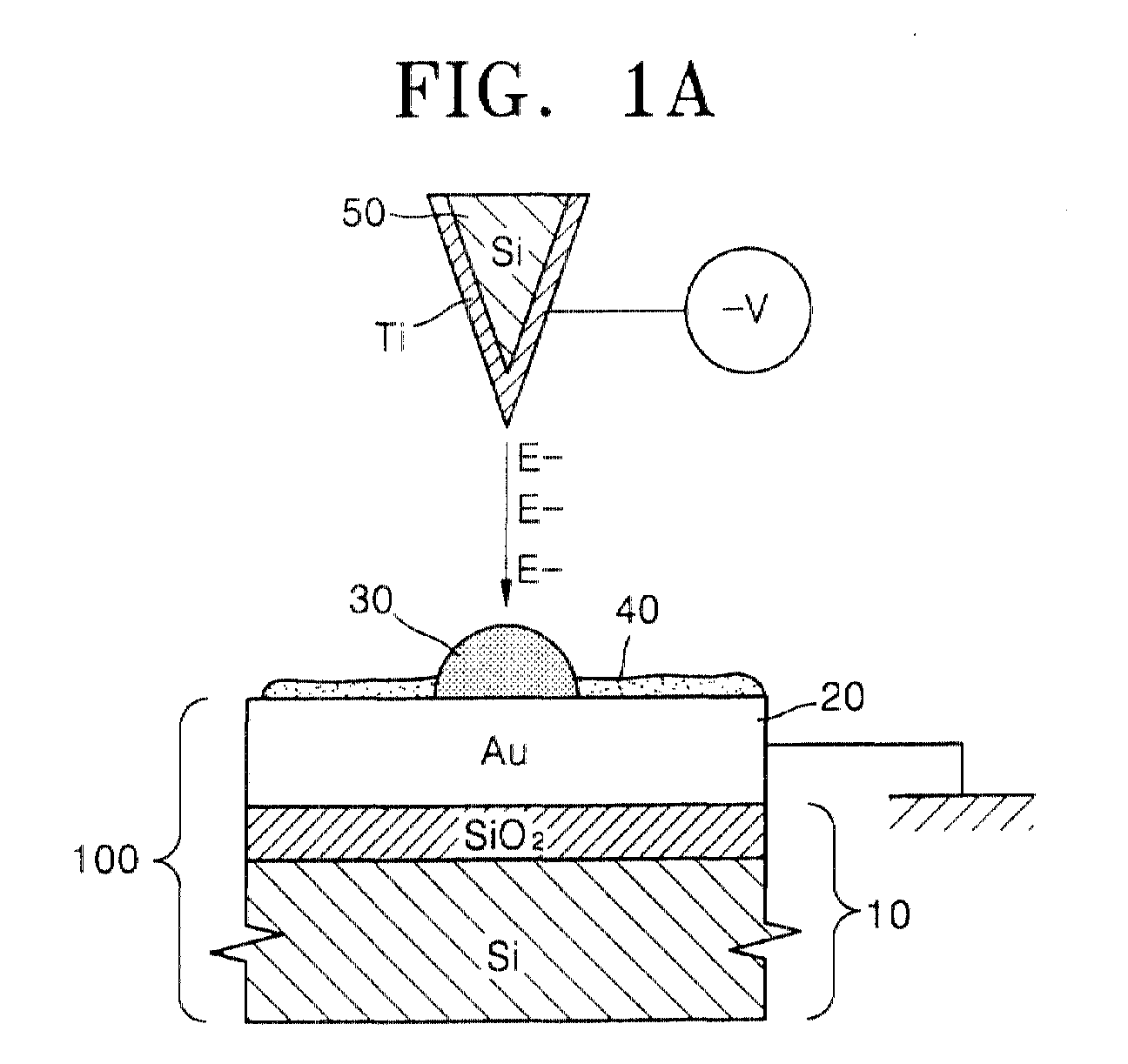
- FIGS. 1A and 1B show the basic structure of an embodiment of a rewritable data storage using carbonaceous material according to the present invention.
- the rewritable data storage includes a substrate, for example, an SiO 2 substrate 10, and an Au/SiO 2 /Si writing plate 100 formed by depositing a conductive layer 20 for example, Au on the substrate 10.
- a cantilever tip 50 is formed for forming or eliminating a carbonaceous material 30 in the form of spots representing information recorded on the conductive layer 20.
- SPM scanning probe microscope
- a reference numeral 40 is an ambient residual gas species such as CO 2 , H 2 O, O 2 , N 2 , CH 4 which can be obtained on the surface of the Au layer in air.
- the rewritable data storage of the above structure employing a carbonaceous material, and the writing/reading method thereof are as follows.
- a bias voltage (V) is applied across the space between the cantilever tip 50 and the Au/SiO 2 /Si writing plate 100, the carbonaceous material 30 is formed on the Au conductive layer 20.
- V bias voltage
- the level of the bias voltage applied across the space between the Au/SiO 2 /Si writing plate 100 and the cantilever tip 50 is changed, the sizes of the carbonaceous material spots become different from each other. Information is read by detecting the shape of the carbonaceous material spots of different sizes.
- a bias voltage (-V) is applied across the space between the cantilever tip 50 and the conductive layer 20(an Au layer) of the portion required for writing using the cantilever tip 50 attached to the AFM, and the carbonaceous material 30 is formed. This step may be called "writing”.
- a bias voltage of the reverse polarity (+V) is applied across the space between the cantilever tip 50 and the conductive layer 20 (an Au layer) of the portion required to be erased using the cantilever tip 50 attached to the AFM, and the carbonaceous material 30 is eliminated. This step may be called "erasing".
- FIGS. 1A and 1B The structural principle of the rewritable data storage using the carbonaceous material as illustrated in FIGS. 1A and 1B is described in detail below.
- the writing plate 100 comprising the conductive layer (an Au layer) 20 formed on the SiO 2 /Si substrate 10, and the cantilever tip 50 comprising Ti coated on the tip-shaped Si core is disposed above the writing pad 100.
- a regular voltage is applied across the space between the conductive layer 20 and the cantilever tip 50 of the writing plate, and electrons are emitted into the air (that is, an electric discharge is caused).
- the emitted electrons locally deposit the carbonaceous material on the conductive layer 20 of the writing plate through an electrochemical reaction with CO 2 , H 2 O, N 2 , O 2 , CH 4 , and so on existing in the air on the conductive layer 20 of the writing plate 100. If the written information is erased, the electrochemical reaction (or a voltage or a current induced electrochemical decomposition/desorption) is caused by applying the voltage of reverse polarity, and the stored carbonaceous material 30 is eliminated from the conductive layer 20.
- FIGS. 2A through 2D Images of the actually formed carbonaceous materials being read with the AFM are illustrated in FIGS. 2A through 2D.
- FIG. 2A is an image of a rectangular carbon microstructure being read by applying -6 V to the tip after writing the carbon microstructure on the Au layer.
- FIG. 2B is an image of the rectangular form of FIG. 2A being read with the AFM after erasing a part, leaving a black part in the center, by applying +5 V to the tip.
- FIG. 2C is an image of the rectangular structure being read with the AFM after erasing three more parts of the original spot form by applying +5 V to the tip.
- FIG. 2D is an image of the rectangular structure being read with the AFM after rewriting information (a white point) in the center which was previously erased, by applying -6 V to the tip. As sequentially illustrated in FIGS.
- the process wherein the carbonaceous material 30 is formed in a specified region on the writing plate 100 (a conductive layer), the formed material is erased, and then the carbonaceous material is formed again in the same position, can be performed by the polarity transformation of the bias voltage applied across the space between the cantilever tip 50 and the conductive layer 20.
- FIG. 3 is an image of spots of the carbonaceous material formed when changing and applying various sizes of the bias voltage applied across the space between the substrate and the tip being read with the AFM.
- the spots of the formed carbonaceous material can be formed to various sizes according to the size of the applied bias voltage or the duration of application.
- the size of the spot of the carbonaceous material formed or eliminated can be controlled by changing the magnitude of the bias voltage as illustrated in FIG. 3.
- the size of the spot can be controlled on the order of tens nm, so that it can be easily applied to the manufacture of a rewritable data storage of hundreds or more Gb class.
- FIG. 4A is an image of a sample used for the AES analysis being read with the AFM, wherein a white part of size 3 ⁇ m ⁇ 4 ⁇ m (P3, P4) is a place where the carbonaceous material is formed by the method previously described (where information is stored), and the conductive layer region where the carbonaceous material is not formed is indicated as P1, P2.
- AES spectrums indicated as P3 and P4 in FIG. 4B are the result of an AES analysis of a place where information is stored.
- AES spectrums indicated as P1 and P2 in FIG. 4B are the result of an AES analysis of the original Au layer where information is not stored.
- striped conductive layer patterns 210 are formed on a substrate 200, a cantilever 225, in which a cantilever tip 220 is formed in an array, is installed above the conductive layer patterns to form a circuit, and then, the carbonaceous material can be formed in the desired place. Also, information of the desired place can be read by selecting a switch 211 and a position of the cantilever, and applying a voltage. That is, as illustrated in FIG.
- the carbonaceous material is not formed.
- the cantilever tip 220 such as AFM tip
- the third conductive layer pattern 210 are selected and a bias voltage (-6 V) is applied
- the carbonaceous material 230 is formed in the selected region of the selected third conductive layer pattern 210.
- a plurality of cantilevers, on each of which tips are formed in an array may be formed so that a data storage capable being accessed while the cantilevers move only a short distance, can be manufactured.
- a rewritable data storage using carbonaceous material writes or erases information, that is the carbonaceous material, by means of a current induced electrochemical reaction on the conductive layer, by controlling a voltage applied across the space between the cantilever tip and the conductive layer. Also, here, the size of the carbonaceous material representing information is controlled by the level of the applied voltage or the application duration.
- the data storage is rewritable but does not employ phase transformation
- the writing/erasing endurance is enhanced, and the deterioration of the material features of the prior art with respect to a continuous write/erase cycle is solved, so that it can be semi-permanently used.
- information can be stored and eliminated by creating or eliminating a structure on the order of tens of nanometers in size, so that a rewritable data storage capable of storing and rewriting more than hundreds of gigabytes of information Gb can be embodied.
Landscapes
- Engineering & Computer Science (AREA)
- Chemical & Material Sciences (AREA)
- Nanotechnology (AREA)
- Physics & Mathematics (AREA)
- Mathematical Physics (AREA)
- Theoretical Computer Science (AREA)
- Crystallography & Structural Chemistry (AREA)
- Semiconductor Memories (AREA)
- Carbon And Carbon Compounds (AREA)
- Electrochromic Elements, Electrophoresis, Or Variable Reflection Or Absorption Elements (AREA)
Abstract
Description
Claims (12)
- A rewritable data storage using a carbonaceous material comprising:a writing plate formed of a substrate and a conductive layer deposited on the substrate; anda tip for forming or eliminating carbonaceous material in the form of spots representing information recorded on the conductive layer.
- The rewritable data storage using a carbonaceous material of claim 1, wherein the substrate is formed of SiO2/Si.
- The rewritable data storage using a carbonaceous material of claim 1 or 2, wherein the conductive layer is formed by depositing Au.
- The rewritable data storage using a carbonaceous material of claim 1, 2 or 3, wherein the tip is formed by coating Ti on a tip -shaped Si core.
- A rewritable data storage according to any preceding claim wherein the conductive layer includes striped conductive layer patterns formed on the substrate; and
a cantilever extending across the striped conductive layer patterns carrying an array of tips having a regular interval to correspond to the striped conductive layer patterns for forming or eliminating carbonaceous material in the form of spots representing information recorded on the conductive layer patterns. - A writing/reading method of a rewritable data storage using a carbonaceous material, the rewritable data storage including: a writing plate formed of a substrate and a conductive layer formed on the substrate; and a tip for forming or eliminating a carbonaceous material in the form of spots representing information recorded on the conductive layer, the writing/reading method comprising:(a) writing information by applying a predetermined bias voltage to the space between the tip and the conductive layer and forming a carbonaceous material on the conductive layer;(b) erasing the information by applying the voltage of reverse polarity to the bias voltage applied in the writing step to the space between the tip and the conductive layer, and eliminating the carbonaceous material already formed; and(c) reading the information by discriminating topography between the conductive layer and the carbonaceous material.
- The writing/reading method of the rewritable data storage using the carbonaceous material of claim 6, wherein, the size of spots of the carbonaceous material formed in step (a) is decided by controlling the magnitude of the bias voltage applied across the space between the conductive layer and the tip or the time duration for which the bias voltage is applied.
- The writing/reading method of the rewritable data storage using the carbonaceous material of claim 6 or 7, wherein the size of spots of the carbonaceous material eliminated in step (b) is decided by controlling the magnitude of the bias voltage applied across the space between the conductive layer and the tip or the time duration for which the bias voltage is applied.
- The writing/reading method of the rewritable data storage using the carbonaceous material of claim 6, 7 or 8, wherein the step (c) is performed using one of a capacitance difference, a resistance difference, a frictional coefficient difference, and a height difference between the conductive layer and the carbonaceous material.
- A writing/reading method of a rewritable data storage according to any of claims 6 to 9 wherein the writing plate comprises a substrate on which striped conductive layer patterns are formed by depositing a conductor on the substrate; and a cantilever extends across the striped conductive layer patterns carrying an array of tips having a regular interval to correspond to the striped conductive layer patterns for forming or eliminating a carbonaceous material in the form of spots representing information recorded on the conductive layer, including:(a) writing information by positioning the cantilever, applying a predetermined bias voltage to the space between the cantilever tip and the selected conductive layer pattern and forming a carbonaceous material in the selected region of the selected conductive layer pattern; and(b) erasing the information by positioning the cantilever, applying the voltage of reverse polarity to the bias voltage applied in the writing step to the space between the cantilever tip and the selected conductive layer pattern, and eliminating the carbonaceous material already formed.
- The writing/reading method of a rewritable data storage using a carbonaceous material of claim 10, wherein the size of spots of the carbonaceous material formed in step (a) is decided by controlling the magnitude of the bias voltage applied across the space between the conductive layer patterns and the cantilever tip, or the time duration for which the bias voltage is applied.
- The writing/reading method of the rewritable data storage using the carbonaceous material of claim 10 or 11, wherein the size of spots of the carbonaceous material eliminated in the step 10 or 11 is decided by controlling the magnitude of the bias voltage applied across the space between the conductive layer patterns and the cantilever tip, or the time duration for which the bias voltage is applied.
Applications Claiming Priority (2)
| Application Number | Priority Date | Filing Date | Title |
|---|---|---|---|
| KR2000025043 | 2000-05-10 | ||
| KR1020000025043A KR100331451B1 (en) | 2000-05-10 | 2000-05-10 | Rewritable data storage using carbonaceous material and writing and reading method thereof |
Publications (3)
| Publication Number | Publication Date |
|---|---|
| EP1154422A2 true EP1154422A2 (en) | 2001-11-14 |
| EP1154422A3 EP1154422A3 (en) | 2003-07-02 |
| EP1154422B1 EP1154422B1 (en) | 2008-12-03 |
Family
ID=19668365
Family Applications (1)
| Application Number | Title | Priority Date | Filing Date |
|---|---|---|---|
| EP01304068A Expired - Lifetime EP1154422B1 (en) | 2000-05-10 | 2001-05-04 | Rewritable data storage using carbonaceous material and writing/reading method therof |
Country Status (6)
| Country | Link |
|---|---|
| US (1) | US7020064B2 (en) |
| EP (1) | EP1154422B1 (en) |
| JP (1) | JP3740032B2 (en) |
| KR (1) | KR100331451B1 (en) |
| CN (1) | CN1162911C (en) |
| DE (1) | DE60136769D1 (en) |
Cited By (4)
| Publication number | Priority date | Publication date | Assignee | Title |
|---|---|---|---|---|
| EP1333436A3 (en) * | 2002-01-31 | 2004-08-04 | Pioneer Corporation | Record condition extraction system and method for a dielectric recording medium, and information recording apparatus |
| US7336590B2 (en) | 2002-09-11 | 2008-02-26 | Yasuo Cho | Dielectric reproducing apparatus, dielectric recording apparatus, and dielectric recording/reproducing apparatus |
| US7385901B2 (en) | 2003-06-12 | 2008-06-10 | Yasuo Cho | Data recording/reproducing apparatus and method using needle-shaped member |
| US7590040B2 (en) | 2003-08-25 | 2009-09-15 | Yasuo Cho | Signal detecting method and apparatus and information reproducing apparatus and method |
Families Citing this family (18)
| Publication number | Priority date | Publication date | Assignee | Title |
|---|---|---|---|---|
| US7260051B1 (en) * | 1998-12-18 | 2007-08-21 | Nanochip, Inc. | Molecular memory medium and molecular memory integrated circuit |
| US6586133B1 (en) * | 2000-02-21 | 2003-07-01 | The University Of Tulsa | Nano-battery systems |
| US20020138301A1 (en) * | 2001-03-22 | 2002-09-26 | Thanos Karras | Integration of a portal into an application service provider data archive and/or web based viewer |
| JP4017104B2 (en) * | 2002-07-09 | 2007-12-05 | パイオニア株式会社 | Dielectric recording / reproducing head and tracking method |
| US7233517B2 (en) | 2002-10-15 | 2007-06-19 | Nanochip, Inc. | Atomic probes and media for high density data storage |
| KR100499136B1 (en) * | 2002-12-14 | 2005-07-04 | 삼성전자주식회사 | Magnetic medium using electron spin-dependent scattering and apparatus of reading data from the same and method thereof |
| WO2004097822A1 (en) * | 2003-05-01 | 2004-11-11 | Pioneer Corporation | Recording/reproduction head and recording/reproduction device |
| US7704615B1 (en) * | 2003-08-07 | 2010-04-27 | The University Of Tulsa | Charged arrays of micro and nanoscale electrochemical cells and batteries for computer and nanodevice memory and power supply |
| FR2862156B1 (en) * | 2003-11-06 | 2007-01-05 | Commissariat Energie Atomique | CONDUCTIVE MICRO-POINT DATA RECORDING DEVICE AND METHOD FOR MANUFACTURING SUCH A DEVICE |
| US20050243660A1 (en) * | 2004-04-16 | 2005-11-03 | Rust Thomas F | Methods for erasing bit cells in a high density data storage device |
| US8574744B1 (en) | 2005-05-13 | 2013-11-05 | The University Of Tulsa | Nanoscale three-dimensional battery architecture |
| US7736724B1 (en) | 2005-05-13 | 2010-06-15 | The University Of Tulsa | Fabrication of nanobaskets by sputter deposition on porous substrates and uses thereof |
| US20070041237A1 (en) * | 2005-07-08 | 2007-02-22 | Nanochip, Inc. | Media for writing highly resolved domains |
| US7463573B2 (en) * | 2005-06-24 | 2008-12-09 | Nanochip, Inc. | Patterned media for a high density data storage device |
| US7367119B2 (en) | 2005-06-24 | 2008-05-06 | Nanochip, Inc. | Method for forming a reinforced tip for a probe storage device |
| US7309630B2 (en) | 2005-07-08 | 2007-12-18 | Nanochip, Inc. | Method for forming patterned media for a high density data storage device |
| US20090129246A1 (en) * | 2007-11-21 | 2009-05-21 | Nanochip, Inc. | Environmental management of a probe storage device |
| US20100039729A1 (en) * | 2008-08-14 | 2010-02-18 | Nanochip, Inc. | Package with integrated magnets for electromagnetically-actuated probe-storage device |
Family Cites Families (18)
| Publication number | Priority date | Publication date | Assignee | Title |
|---|---|---|---|---|
| US4550257A (en) * | 1984-06-29 | 1985-10-29 | International Business Machines Corporation | Narrow line width pattern fabrication |
| JPH01125746A (en) * | 1987-11-10 | 1989-05-18 | Nippon Telegr & Teleph Corp <Ntt> | Method for erasing record in memory device |
| JP2557964B2 (en) * | 1988-01-22 | 1996-11-27 | インターナシヨナル・ビジネス・マシーンズ・コーポレイーシヨン | Data storage |
| JPH0298896A (en) * | 1988-10-05 | 1990-04-11 | Olympus Optical Co Ltd | Memory |
| US5241527A (en) * | 1989-03-16 | 1993-08-31 | Canon Kabushiki Kaisha | Recording and reproducing apparatus and method using a recording layer having a positioning region |
| DE69127381T2 (en) * | 1990-01-19 | 1998-01-22 | Canon Kk | Information processing system and information processing method |
| US5043578A (en) * | 1990-04-05 | 1991-08-27 | International Business Machines Corporation | Writing atomic scale features with fine tip as source of deposited atoms |
| JPH041949A (en) * | 1990-04-18 | 1992-01-07 | Canon Inc | Information input and/or retrieval device |
| US5047649A (en) * | 1990-10-09 | 1991-09-10 | International Business Machines Corporation | Method and apparatus for writing or etching narrow linewidth patterns on insulating materials |
| US5216631A (en) * | 1990-11-02 | 1993-06-01 | Sliwa Jr John W | Microvibratory memory device |
| JPH0536128A (en) * | 1990-12-20 | 1993-02-12 | Hitachi Ltd | High density information recording medium and recording device using the same |
| JP3109861B2 (en) * | 1991-06-12 | 2000-11-20 | キヤノン株式会社 | Information recording and / or reproducing apparatus |
| JP2794348B2 (en) * | 1991-06-21 | 1998-09-03 | キヤノン株式会社 | Recording medium, manufacturing method thereof, and information processing apparatus |
| DE69232806T2 (en) * | 1991-07-17 | 2003-02-20 | Canon K.K., Tokio/Tokyo | Information recording / reproducing apparatus or method for information recording / reproducing on / from an information recording medium using a plurality of probe electrodes |
| JP2923190B2 (en) * | 1993-12-16 | 1999-07-26 | シャープ株式会社 | High density recording medium and recording / reproducing apparatus therefor |
| KR950024146A (en) * | 1994-01-31 | 1995-08-21 | 모리시타 요이찌 | Information recording and reproducing apparatus and information recording and reproducing method |
| JPH08315433A (en) * | 1995-05-15 | 1996-11-29 | Canon Inc | Information processing apparatus and information processing method |
| JP3519623B2 (en) * | 1998-03-13 | 2004-04-19 | 株式会社東芝 | Recording medium and method for manufacturing the same |
-
2000
- 2000-05-10 KR KR1020000025043A patent/KR100331451B1/en not_active Expired - Fee Related
-
2001
- 2001-05-04 EP EP01304068A patent/EP1154422B1/en not_active Expired - Lifetime
- 2001-05-04 DE DE60136769T patent/DE60136769D1/en not_active Expired - Lifetime
- 2001-05-08 JP JP2001137107A patent/JP3740032B2/en not_active Expired - Fee Related
- 2001-05-10 US US09/852,300 patent/US7020064B2/en not_active Expired - Lifetime
- 2001-05-10 CN CNB011177373A patent/CN1162911C/en not_active Expired - Lifetime
Cited By (6)
| Publication number | Priority date | Publication date | Assignee | Title |
|---|---|---|---|---|
| EP1333436A3 (en) * | 2002-01-31 | 2004-08-04 | Pioneer Corporation | Record condition extraction system and method for a dielectric recording medium, and information recording apparatus |
| US6912193B2 (en) | 2002-01-31 | 2005-06-28 | Yasuo Cho | Record condition extraction system and method of dielectric recording medium, and information recording apparatus |
| US7336590B2 (en) | 2002-09-11 | 2008-02-26 | Yasuo Cho | Dielectric reproducing apparatus, dielectric recording apparatus, and dielectric recording/reproducing apparatus |
| US7385901B2 (en) | 2003-06-12 | 2008-06-10 | Yasuo Cho | Data recording/reproducing apparatus and method using needle-shaped member |
| US8004948B2 (en) | 2003-06-12 | 2011-08-23 | Yasuo Cho | Data recording / reproducing apparatus and method using needle-shaped member |
| US7590040B2 (en) | 2003-08-25 | 2009-09-15 | Yasuo Cho | Signal detecting method and apparatus and information reproducing apparatus and method |
Also Published As
| Publication number | Publication date |
|---|---|
| DE60136769D1 (en) | 2009-01-15 |
| EP1154422A3 (en) | 2003-07-02 |
| US7020064B2 (en) | 2006-03-28 |
| KR20010103899A (en) | 2001-11-24 |
| EP1154422B1 (en) | 2008-12-03 |
| JP3740032B2 (en) | 2006-01-25 |
| CN1323066A (en) | 2001-11-21 |
| US20020009632A1 (en) | 2002-01-24 |
| JP2002025134A (en) | 2002-01-25 |
| KR100331451B1 (en) | 2002-04-09 |
| CN1162911C (en) | 2004-08-18 |
Similar Documents
| Publication | Publication Date | Title |
|---|---|---|
| EP1154422B1 (en) | Rewritable data storage using carbonaceous material and writing/reading method therof | |
| US5144581A (en) | Apparatus including atomic probes utilizing tunnel current to read, write and erase data | |
| Tanaka et al. | Scanning nonlinear dielectric microscopy nano-science and technology for next generation high density ferroelectric data storage | |
| US5495109A (en) | Electrochemical identification of molecules in a scanning probe microscope | |
| CA2046063A1 (en) | Storage of information units in the nanometer range | |
| JPS6180536A (en) | Apparatus and method for recording and reading atom-size density information | |
| US7782741B2 (en) | Probe-scanned ferroelectric media with imprinted regions | |
| EP1486966B1 (en) | Data recording / reproducing apparatus and method using needle-shaped member | |
| US5375087A (en) | Tunneling-stabilized magnetic reading and recording | |
| CN101136226A (en) | Information recording and reproducing device | |
| US7539119B2 (en) | Data storage apparatus using current switching in metal oxide layer | |
| JP3029143B2 (en) | Information playback method | |
| US5740101A (en) | Time-stable labeling of individual atoms or groups of atoms in the surface of a solid, and the storage of information units in the atomic range | |
| Quate | Surface modification with the STM and the AFM | |
| EP0449409A2 (en) | Probe unit, information processing device using same and methods of use and manufacture | |
| US8374071B2 (en) | Data storage device | |
| Kim et al. | Near-field optical readout combined with atomic force probe recording | |
| US20080025191A1 (en) | Data storage device | |
| JP3118654B2 (en) | Information processing device and scanning tunneling electron microscope | |
| JP3937486B2 (en) | Recording apparatus and recording / reproducing apparatus | |
| JPH1083586A (en) | Recording and playback device | |
| IE911565A1 (en) | Time-stable labeling of individual atoms or groups of atoms¹in the surface of a solid, and the storage of information¹units in the atomic range | |
| JPH10289495A (en) | Recording and playback device | |
| JPH04349243A (en) | Smooth electrode substrate, recording medium and information processor | |
| JPH08235653A (en) | Scanning probe recording / reproducing device |
Legal Events
| Date | Code | Title | Description |
|---|---|---|---|
| PUAI | Public reference made under article 153(3) epc to a published international application that has entered the european phase |
Free format text: ORIGINAL CODE: 0009012 |
|
| AK | Designated contracting states |
Kind code of ref document: A2 Designated state(s): AT BE CH CY DE DK ES FI FR GB GR IE IT LI LU MC NL PT SE TR |
|
| AX | Request for extension of the european patent |
Free format text: AL;LT;LV;MK;RO;SI |
|
| 17P | Request for examination filed |
Effective date: 20011212 |
|
| PUAL | Search report despatched |
Free format text: ORIGINAL CODE: 0009013 |
|
| AK | Designated contracting states |
Designated state(s): AT BE CH CY DE DK ES FI FR GB GR IE IT LI LU MC NL PT SE TR |
|
| AX | Request for extension of the european patent |
Extension state: AL LT LV MK RO SI |
|
| AKX | Designation fees paid |
Designated state(s): DE FR GB |
|
| 17Q | First examination report despatched |
Effective date: 20061222 |
|
| GRAP | Despatch of communication of intention to grant a patent |
Free format text: ORIGINAL CODE: EPIDOSNIGR1 |
|
| GRAS | Grant fee paid |
Free format text: ORIGINAL CODE: EPIDOSNIGR3 |
|
| GRAA | (expected) grant |
Free format text: ORIGINAL CODE: 0009210 |
|
| AK | Designated contracting states |
Kind code of ref document: B1 Designated state(s): DE FR GB |
|
| REG | Reference to a national code |
Ref country code: GB Ref legal event code: FG4D |
|
| REF | Corresponds to: |
Ref document number: 60136769 Country of ref document: DE Date of ref document: 20090115 Kind code of ref document: P |
|
| PLBE | No opposition filed within time limit |
Free format text: ORIGINAL CODE: 0009261 |
|
| STAA | Information on the status of an ep patent application or granted ep patent |
Free format text: STATUS: NO OPPOSITION FILED WITHIN TIME LIMIT |
|
| 26N | No opposition filed |
Effective date: 20090904 |
|
| GBPC | Gb: european patent ceased through non-payment of renewal fee |
Effective date: 20090504 |
|
| REG | Reference to a national code |
Ref country code: FR Ref legal event code: ST Effective date: 20100129 |
|
| PG25 | Lapsed in a contracting state [announced via postgrant information from national office to epo] |
Ref country code: FR Free format text: LAPSE BECAUSE OF NON-PAYMENT OF DUE FEES Effective date: 20090602 |
|
| PG25 | Lapsed in a contracting state [announced via postgrant information from national office to epo] |
Ref country code: GB Free format text: LAPSE BECAUSE OF NON-PAYMENT OF DUE FEES Effective date: 20090504 |
|
| PGFP | Annual fee paid to national office [announced via postgrant information from national office to epo] |
Ref country code: DE Payment date: 20200421 Year of fee payment: 20 |
|
| REG | Reference to a national code |
Ref country code: DE Ref legal event code: R071 Ref document number: 60136769 Country of ref document: DE |