EP1102163A2 - Microprocessor with improved instruction set architecture - Google Patents
Microprocessor with improved instruction set architecture Download PDFInfo
- Publication number
- EP1102163A2 EP1102163A2 EP00310098A EP00310098A EP1102163A2 EP 1102163 A2 EP1102163 A2 EP 1102163A2 EP 00310098 A EP00310098 A EP 00310098A EP 00310098 A EP00310098 A EP 00310098A EP 1102163 A2 EP1102163 A2 EP 1102163A2
- Authority
- EP
- European Patent Office
- Prior art keywords
- field
- instruction
- circuitry
- bit
- register
- Prior art date
- Legal status (The legal status is an assumption and is not a legal conclusion. Google has not performed a legal analysis and makes no representation as to the accuracy of the status listed.)
- Withdrawn
Links
Images


Classifications
-
- G—PHYSICS
- G06—COMPUTING OR CALCULATING; COUNTING
- G06F—ELECTRIC DIGITAL DATA PROCESSING
- G06F9/00—Arrangements for program control, e.g. control units
- G06F9/06—Arrangements for program control, e.g. control units using stored programs, i.e. using an internal store of processing equipment to receive or retain programs
- G06F9/30—Arrangements for executing machine instructions, e.g. instruction decode
- G06F9/38—Concurrent instruction execution, e.g. pipeline or look ahead
- G06F9/3885—Concurrent instruction execution, e.g. pipeline or look ahead using a plurality of independent parallel functional units
- G06F9/3889—Concurrent instruction execution, e.g. pipeline or look ahead using a plurality of independent parallel functional units controlled by multiple instructions, e.g. MIMD, decoupled access or execute
- G06F9/3891—Concurrent instruction execution, e.g. pipeline or look ahead using a plurality of independent parallel functional units controlled by multiple instructions, e.g. MIMD, decoupled access or execute organised in groups of units sharing resources, e.g. clusters
-
- G—PHYSICS
- G06—COMPUTING OR CALCULATING; COUNTING
- G06F—ELECTRIC DIGITAL DATA PROCESSING
- G06F9/00—Arrangements for program control, e.g. control units
- G06F9/06—Arrangements for program control, e.g. control units using stored programs, i.e. using an internal store of processing equipment to receive or retain programs
- G06F9/30—Arrangements for executing machine instructions, e.g. instruction decode
- G06F9/30003—Arrangements for executing specific machine instructions
- G06F9/30007—Arrangements for executing specific machine instructions to perform operations on data operands
- G06F9/3001—Arithmetic instructions
- G06F9/30014—Arithmetic instructions with variable precision
-
- G—PHYSICS
- G06—COMPUTING OR CALCULATING; COUNTING
- G06F—ELECTRIC DIGITAL DATA PROCESSING
- G06F9/00—Arrangements for program control, e.g. control units
- G06F9/06—Arrangements for program control, e.g. control units using stored programs, i.e. using an internal store of processing equipment to receive or retain programs
- G06F9/30—Arrangements for executing machine instructions, e.g. instruction decode
- G06F9/30003—Arrangements for executing specific machine instructions
- G06F9/30007—Arrangements for executing specific machine instructions to perform operations on data operands
- G06F9/30036—Instructions to perform operations on packed data, e.g. vector, tile or matrix operations
-
- G—PHYSICS
- G06—COMPUTING OR CALCULATING; COUNTING
- G06F—ELECTRIC DIGITAL DATA PROCESSING
- G06F9/00—Arrangements for program control, e.g. control units
- G06F9/06—Arrangements for program control, e.g. control units using stored programs, i.e. using an internal store of processing equipment to receive or retain programs
- G06F9/30—Arrangements for executing machine instructions, e.g. instruction decode
- G06F9/30098—Register arrangements
- G06F9/30105—Register structure
- G06F9/30112—Register structure comprising data of variable length
-
- G—PHYSICS
- G06—COMPUTING OR CALCULATING; COUNTING
- G06F—ELECTRIC DIGITAL DATA PROCESSING
- G06F9/00—Arrangements for program control, e.g. control units
- G06F9/06—Arrangements for program control, e.g. control units using stored programs, i.e. using an internal store of processing equipment to receive or retain programs
- G06F9/30—Arrangements for executing machine instructions, e.g. instruction decode
- G06F9/30098—Register arrangements
- G06F9/3012—Organisation of register space, e.g. banked or distributed register file
-
- G—PHYSICS
- G06—COMPUTING OR CALCULATING; COUNTING
- G06F—ELECTRIC DIGITAL DATA PROCESSING
- G06F9/00—Arrangements for program control, e.g. control units
- G06F9/06—Arrangements for program control, e.g. control units using stored programs, i.e. using an internal store of processing equipment to receive or retain programs
- G06F9/30—Arrangements for executing machine instructions, e.g. instruction decode
- G06F9/34—Addressing or accessing the instruction operand or the result ; Formation of operand address; Addressing modes
- G06F9/355—Indexed addressing
- G06F9/3555—Indexed addressing using scaling, e.g. multiplication of index
-
- G—PHYSICS
- G06—COMPUTING OR CALCULATING; COUNTING
- G06F—ELECTRIC DIGITAL DATA PROCESSING
- G06F9/00—Arrangements for program control, e.g. control units
- G06F9/06—Arrangements for program control, e.g. control units using stored programs, i.e. using an internal store of processing equipment to receive or retain programs
- G06F9/30—Arrangements for executing machine instructions, e.g. instruction decode
- G06F9/38—Concurrent instruction execution, e.g. pipeline or look ahead
- G06F9/3824—Operand accessing
- G06F9/3826—Bypassing or forwarding of data results, e.g. locally between pipeline stages or within a pipeline stage
- G06F9/3828—Bypassing or forwarding of data results, e.g. locally between pipeline stages or within a pipeline stage with global bypass, e.g. between pipelines, between clusters
-
- G—PHYSICS
- G06—COMPUTING OR CALCULATING; COUNTING
- G06F—ELECTRIC DIGITAL DATA PROCESSING
- G06F9/00—Arrangements for program control, e.g. control units
- G06F9/06—Arrangements for program control, e.g. control units using stored programs, i.e. using an internal store of processing equipment to receive or retain programs
- G06F9/30—Arrangements for executing machine instructions, e.g. instruction decode
- G06F9/38—Concurrent instruction execution, e.g. pipeline or look ahead
- G06F9/3836—Instruction issuing, e.g. dynamic instruction scheduling or out of order instruction execution
- G06F9/3853—Instruction issuing, e.g. dynamic instruction scheduling or out of order instruction execution of compound instructions
-
- G—PHYSICS
- G06—COMPUTING OR CALCULATING; COUNTING
- G06F—ELECTRIC DIGITAL DATA PROCESSING
- G06F9/00—Arrangements for program control, e.g. control units
- G06F9/06—Arrangements for program control, e.g. control units using stored programs, i.e. using an internal store of processing equipment to receive or retain programs
- G06F9/30—Arrangements for executing machine instructions, e.g. instruction decode
- G06F9/38—Concurrent instruction execution, e.g. pipeline or look ahead
- G06F9/3885—Concurrent instruction execution, e.g. pipeline or look ahead using a plurality of independent parallel functional units
Definitions
- This invention relates to data processing devices, electronic processing and control systems and methods of their manufacture and operation, and particularly relates to microprocessors optimized for digital signal processing.
- a microprocessor is a circuit that combines the instruction-handling, arithmetic, and logical operations of a computer on a single semiconductor integrated circuit.
- Microprocessors can be grouped into two general classes, namely general-purpose microprocessors and special-purpose microprocessors.
- General-purpose microprocessors are designed to be programmable by the user to perform any of a wide range of tasks, and are therefore often used as the central processing unit (CPU) in equipment such as personal computers.
- Special-purpose microprocessors in contrast, are designed to provide performance improvement for specific predetermined arithmetic and logical functions for which the user intends to use the microprocessor.
- the designer can structure the microprocessor architecture in such a manner that the performance of the specific function by the special-purpose microprocessor greatly exceeds the performance of the same function by a general-purpose microprocessor regardless of the program implemented by the user.
- Digital signal processing generally involves the representation, transmission, and manipulation of signals, using numerical techniques and a type of special-purpose microprocessor known as a digital signal processor (DSP).
- DSP digital signal processor
- Digital signal processing typically requires the manipulation of large volumes of data, and a digital signal processor is optimized to efficiently perform the intensive computation and memory access operations associated with this data manipulation. For example, computations for performing Fast Fourier Transforms (FFTs) and for implementing digital filters consist to a large degree of repetitive operations such as multiply-and-add and multiple-bit-shift.
- FFTs Fast Fourier Transforms
- DSPs can be specifically adapted for these repetitive functions, and provide a substantial performance improvement over general-purpose microprocessors in, for example, real-time applications such as image and speech processing.
- DSPs are central to the operation of many of today's electronic products, such as high-speed modems, high-density disk drives, digital cellular phones, complex automotive systems, and video-conferencing equipment. DSPs will enable a wide variety of other digital systems in the future, such as video-phones, network processing, natural speech interfaces, and ultra-high speed modems. The demands placed upon DSPs in these and other applications continue to grow as consumers seek increased performance from their digital products, and as the convergence of the communications, computer and consumer industries creates completely new digital products.
- Microprocessor designers have increasingly endeavored to exploit parallelism to improve performance.
- One parallel architecture that has found application in some modern microprocessors utilizes multiple instruction fetch packets and multiple instruction execution packets with multiple functional units.
- ASIC application specific integrated circuit
- MegaModules are being used in the design of ASICsto create complex digital systems a single chip.
- Types of MegaModules include SRAMs, FIFOs, register files, RAMs, ROMs, universal asynchronous receiver-transmitters (UARTs), programmable logic arrays and other such logic circuits.
- MegaModules are usually defined as integrated circuit modules of at least 500 gates in complexity and having a complex ASIC macro function. These MegaModules are predesigned and stored in an ASIC design library. The MegaModules can then be selected by a designer and placed within a certain area on a new IC chip.
- the invention provides a microprocessor having an instruction execution pipeline with a plurality of pipeline phases, comprising:
- program fetch circuitry operable to fetch instructions; instruction decode circuitry connected to receive fetched instructions from the program fetch circuitry, the instruction decode circuitry operable to decode a set of single instruction, multiple data (SIMD) instructions; and
- the microprocessor further comprises a second functional unit connected to operate in parallel with the first functional unit, wherein the second functional unit comprises multi-field multiplication circuitry connected to receive a plurality of source operands and having outputs connected to provide a multi-field result as a destination operand in response to control signals from the instruction decode circuitry, wherein the multi-field multiplication circuitry is operable to treat the plurality of source operands as a set of N2 fields, such that the multi-field result includes N2 results corresponding to the set of N2 fields; and wherein the second functional unit is operable to provide the multi-field result in response to a single SIMD instruction of a second type.
- the second functional unit comprises multi-field multiplication circuitry connected to receive a plurality of source operands and having outputs connected to provide a multi-field result as a destination operand in response to control signals from the instruction decode circuitry, wherein the multi-field multiplication circuitry is operable to treat the plurality of source operands as a set of N2 fields
- the microprocessor further comprises:
- the first storage register is part of a register file connected to the first functional unit and to the second functional unit for providing the plurality of source operands and connected to the first functional unit and to the second function unit to receive the destination operands.
- the instructions of the first type, second type and third type all have a field for identifying a predicate register.
- the microprocessor is included in a digital system and, preferably, the digital system is a cellular telephone, further comprising:
- the invention provides a method of operating a microprocessor, comprising the steps of:
- a method of operating a microprocessor comprises the steps of:
- the method further comprises the step of providing load/store circuitry operable to transfer a multi-byte data item to a memory circuit at a byte address that is not word aligned.
- An illustrative embodiment of the present invention seeks to provide a microprocessor, and a method for operating a microprocessor that improves digital signal processing performance. Aspects of the invention are specified in the claims.
- a digital signal processor which has improvements over prior art devices including: register file enhancements, data path extensions, additional functional unit hardware, increased orthogonality of the instruction set, data flow enhancements/SIMD operation, and additional instructions that reduce code size and increase register flexibility.
- data flow enhancements include: an extensive collection of PACK and byte shift instructions which simplifies manipulation of packed data types; Single Instruction, Multiple Data (SIMD) instructions that operate directly on packed data to streamline data flow and increase instruction set efficiency, including:
- FIG. 1 is a block diagram of a microprocessor 1 which has an embodiment of the present invention.
- Microprocessor 1 is a VLIW digital signal processor ("DSP").
- DSP VLIW digital signal processor
- Figure 1 only shows those portions of microprocessor 1 that are relevant to an understanding of an embodiment of the present invention. Details of general construction for DSPs are well known, and may be found readily elsewhere.
- U.S. Patent 5,072,418 issued to Frederick Boutaud, et al describes a DSP in detail and is incorporated herein by reference.
- U.S. Patent 5,329,471 issued to Gary Swoboda, et al describes in detail how to test and emulate a DSP and is incorporated herein by reference. Details of portions of microprocessor 1 relevant to an embodiment of the present invention are explained in sufficient detail hereinbelow, so as to enable one of ordinary skill in the microprocessor art to make and use the invention.
- CPU 10 central processing unit
- CPU 10 data memory 22, program memory 23, peripherals 60 and an external memory interface (EMIF) with a direct memory access (DMA) 61.
- CPU 10 further has an instruction fetch/decode unit 10a-c, a plurality of execution units, including an arithmetic and load/store unit D1, a multiplier M1, an ALU/shifter unit S1, an arithmetic logic unit (“ALU”) L1, a shared multiport register file 20a from which data are read and to which data are written. Instructions are fetched by fetch unit 10a from instruction memory 23 over a set of busses 41.
- Decoded instructions are provided from the instruction fetch/decode unit 10a-c to the functional units D1, M1, S1, and L1 over various sets of control lines which are not shown.
- Data are provided to/from the register file 20a from/to to load/store units D1 over a first set of busses 32a, to multiplier M1 over a second set of busses 34a, to ALU/shifter unit S1 over a third set of busses 36a and to ALU L1 over a fourth set of busses 38a.
- Data are provided to/from the memory 22 from/to the load/store units D1 via a fifth set of busses 40a. Note that the entire data path described above is duplicated with register file 20b and execution units D2, M2, S2, and L2.
- two unrelated aligned double word (64 bits) load/store transfers can be made in parallel between CPU 10 and data memory 22 on each clock cycle using bus set 40a and bus set 40b.
- a single non-aligned double word load/store transfer is performed by scheduling a first .D unit resource and two load/store ports on memory 22.
- an extraction circuit is connected to the memory subsystem to provide a non-aligned data item extracted from two aligned data items requested by the .D unit.
- a second .D unit can perform 32-bit logical or arithmetic instructions in addition to the .S and .L units while the address port of the second .D unit is being used to transmit one of two contiguous addresses provided by the first .D unit.
- a non-aligned access near the end of a circular buffer region in the target memory provides a non-aligned data item that wraps around to the other end of the circular buffer
- Emulation circuitry 50 provides access to the internal operation of integrated circuit 1 that can be controlled by an external test/development system (XDS) 51.
- External test system 51 is representative of a variety of known test systems for debugging and emulating integrated circuits. One such system is described in U.S. Patent 5,535,331, which is incorporated herein by reference.
- Test circuitry 52 contains control registers and parallel signature analysis circuitry for testing integrated circuit 1.
- memory 22 and memory 23 are shown in Figure 1 to be a part of a microprocessor 1 integrated circuit, the extent of which is represented by the box 42.
- the memories 22-23 could just as well be external to the microprocessor 1 integrated circuit 42, or part of it could reside on the integrated circuit 42 and part of it be external to the integrated circuit 42. These are matters of design choice. Also, the particular selection and number of execution units are a matter of design choice, and are not critical to the invention.
- RAM Random Access Memory
- ROM Read Only Memory
- Disk 72 Disk 72
- Bus 73 is connected to the External Memory Interface (EMIF) which is part of functional block 61 within microprocessor 1.
- EMIF External Memory Interface
- DMA controller is also included within block 61. The DMA controller is generally used to move data between memory and peripherals within microprocessor 1 and memory and peripherals which are external to microprocessor 1.
- CPU core 10 is encapsulated as a MegaModule, however, other embodiments of the present invention may be in custom designed CPU's or mass market microprocessors, for example.
- FIG 2A is a block diagram of the execution units and register files of the microprocessor of Figure 1 and shows a more detailed view of the buses connecting the various functional blocks.
- all data busses are 32 bits wide, unless otherwise noted.
- the general-purpose registers can be used for data, data address pointers, or condition registers. Any number of reads of a given register can be performed in a given cycle.
- the general-purpose register files support data ranging in size from packed 8-bit data through 64-bit fixed-point data. Values larger than 32 bits, such as 40-bit long and 64-bit double word quantities, are stored in register pairs, with the 32 LSBs of data placed in an even-numbered register and the remaining 8 or 32 MSBs in the next upper register (which is always an odd-numbered register). Packed data types store either four 8-bit values or two 16-bit values in a single 32-bit register.
- Figure 7 illustrates the register storage scheme for 40-bit data. Operations requiring a long input ignore the 24 MSBs of the odd register. Operations producing a long result zero-fill the 24 MSBs of the odd register.
- the even register is encoded in the opcode.
- the eight functional units in processor 10's data paths are be divided into two groups of four; each functional unit in one data path is almost identical to the corresponding unit in the other data path.
- the functional units are described in Table 2.
- processor 10 also contains many 8-bit and 16-bit data instructions in the instruction set.
- the MPYU4 instruction performs four 8x8 unsigned multiplies with a single instruction on a .M unit.
- the ADD4 instruction performs four 8-bit additions with a single instruction on a .L unit.
- Each functional unit has its own 32-bit write port into a general-purpose register file (Refer to Figure 2A). All units ending in 1 (for example, .L1) write to register file A 20a and all units ending in 2 write to register file B 20b. Each functional unit has two 32-bit read ports for source operands src1 and src2. Four units (.L1, .L2, .S1, and .S2) have an extra 8-bit-wide port for 40-bit long writes, as well as an 8-bit input for 40-bit long reads. Because each unit has its own 32-bit write port, when performing 32 bit operations all eight units can be used in parallel every cycle. Since each multiplier can return up to a 64-bit result, two write ports are provided from the multipliers to the register file.
- Each functional unit reads directly from and writes directly to the register file within its own data path. That is, the .L1, .S1, .D1, and .M1 units write to register file A and the .L2, .S2, .D2, and .M2 units write to register file B.
- the register files are connected to the opposite-side register file's functional units via the 1X and 2X cross paths. These cross paths allow functional units from one data path to access a 32-bit operand from the opposite side's register file.
- the 1X cross path allows data path A's functional units to read their source from register file B.
- the 2X cross path allows data path B's functional units to read their source from register file A.
- All eight of the functional units have access to the opposite side's register file via a cross path.
- the .M1, .M2, .S1, .S2, .D1 and .D2 units' src2 inputs are selectable between the cross path and the same side register file.
- both src1 and src2 inputs are also selectable between the cross path and the same-side register file.
- cross paths 1X and 2X Only two cross paths, 1X and 2X, exist in this embodiment of the architecture.
- the limit is one source read from each data path's opposite register file per cycle, or a total of two cross-path source reads per cycle.
- multiple units on a side may read the same cross-path source simultaneously.
- the cross path operand for one side may be used by any one, multiple or all the functional units on that side in an execute packet. In the C62x/C67x, only one functional unit per data path, per execute packet could get an operand from the opposite register file.
- a delay clock cycle is introduced whenever an instruction attempts to read a register via a cross path that was updated in the previous cycle. This is known as a cross path stall. This stall is inserted automatically by the hardware; no NOP instruction is needed. It should be noted that no stall is introduced if the register being read is the destination for data loaded by a LDx instruction.
- Processor 10 supports double word loads and stores. There are four 32-bit paths for loading data for memory to the register file. For side A, LD1a is the load path for the 32 LSBs; LD1b is the load path for the 32 MSBs. For side B, LD2a is the load path for the 32 LSBs; LD2b is the load path for the 32 MSBs. There are also four 32-bit paths, for storing register values to memory from each register file. ST1a is the write path for the 32 LSBs on side A; ST1b is the write path for the 32 MSBs for side A. For side B, ST2a is the write path for the 32 LSBs; ST2b is the write path for the 32 MSBs.
- Some of the ports for long and double word operands are shared between functional units. This places a constraint on which long or double word operations can be scheduled on a datapath in the same execute packet.
- Bus 40a has an address bus DA1 which is driven by mux 200a. This allows an address generated by either load/store unit D1 or D2 to provide a memory address for loads or stores for register file 20a.
- Data Bus LD1 loads data from an address in memory 22 specified by address bus DA1 to a register in load unit D1. Unit D1 may manipulate the data provided prior to storing it in register file 20a. Likewise, data bus ST1 stores data from register file 20a to memory 22.
- Load/store unit D1 performs the following operations: 32-bit add, subtract, linear and circular address calculations.
- Load/store unit D2 operates similarly to unit D1, with the assistance of mux 200b for selecting an address.
- T1 and T2 The DA1 and DA2 resources and their associated data paths are specified as T1 and T2 respectively.
- T1 consists of the DA1 address path and the LD1a, LD1b, ST1a and ST1b data paths.
- T2 consists of the DA2 address path and the LD2a, LD2b, ST2a and ST2b data paths.
- the T1 and T2 designations appear in functional unit fields for load and store instructions.
- the following load instruction uses the .D1 unit to generate the address but is using the LD2a path resource from DA2 to place the data in the B register file.
- the use of the DA2 resource is indicated with the T2 designation. LDW .D1T2 *A0[3], B1
- Figure 2B is a top level block diagram of .L unit 18a or 18b, which is optimized to handle logical operations, although hardware is available for a set of add and subtract operations and also for the multi-field intermingling instruction of the present invention.
- Logic block 700 performs various Boolean logic functions. Pass gates 700a together with keeper gates 700b form a latch to hold the contents of a first source operand srcl, which is selected from either register file 20a or 20b via mux 211 (see Figure 2A). Similarly, pass gates 700ca together with keeper gates 700d form a latch to hold the contents of a second source operand src2, which is selected from either register file 20a or 20b via mux 212 (see Figure 2).
- Multiplexer block 702 provides byte intermingling. Pass gates and keeper gates hold first and second source operands srcl and src2.
- Left Most Bit Detection (LMBD) block 704 performs leftmost bit detection in src2 or long_src and src2 as specified by srcl.
- First Adder block 706 performs 40-bit arithmetic using long_src and src2 and sign extended srcl.
- Second Adder block 708 performs multi-field arithmetic on packed data fields in srcl and src2.
- Long mux 710 selects from either the long_src LNG or the eight msbs ADD1(39:32) output from 40-bit adder 706 to odd-destination mux 720.
- Other mux 712 selects from the outputs of logic block 700, mux block 702, LMBD block 704, first adder block 706, second adder block 708 and src1.
- Other mux 712 is divided into four 8-bit sub-blocks that can each be controlled to select respective portions of the six sets of inputs.
- Odd destination mux 720 selects from the outputs of a scan register SCAN31:0 (not shown), the first adder 706 bits ADD1(31:0), long mux 710, other mux 712 and zeros or ones. Odd mux 720 is divided into three separately controlled sections for bits 31:16, 15:8 and 7:0. Even destination register 722 selects from the outputs of a scan register SCAN31:0 (not shown), the first adder 706 bits ADD1(31:0), other mux 712 and zeros or ones. Even mux 722 is divided into two separately controlled sections for bits 31:16 and 15:0.
- Figure 2C is a top level block diagram of .S unit 16a, which is optimized to handle arithmetic, logical, and shifting and also for the multi-field saturation instructions of the present invention.
- the .S unit receives source operand one on inputs 700 and source operand two on inputs 702. An additional 8-bit source input is received on inputs 704 for long source operands. A destination operand output is provided output 710, while a long portion of a destination operand is provided on outputs 712.
- the .S unit has five major functional units: branch circuitry 720, logical function circuitry 722, adder functional circuitry 724, pack/unpack functional circuitry 726, and shifter circuitry 728.
- the lower 32 bits (bits 31:0) of a result are selected by results multiplexer 730 and are stored in the even register of a register pair via outputs 710.
- the upper 8 bits (bits 39:33) of a long result are selected by multiplexer 730 and are stored in the odd register of the register pair via outputs 712.
- Multi-field pack/unpack circuitry 728 performs multi-field packing and unpacking operations as well as multi-field saturation.
- Multi-field circuitry 228 also performs shifting of signed and unsigned packed data.
- Multi-field packing and unpacking can also be performed in .L functional units 18a, 18b and is described in detail in coassigned U.S. Patent application Serial No. (TI-30561) Microprocessor Having a Set of Byte Intermingling Instructions and is incorporated herein by reference.
- FIG 2D is a top level block diagram of .M unit 14a, which is optimized to handle multiplication, although hardware is available for a limited set of non-multiply operations.
- multiplier units M1, M2 are each similar and will be described in more detail with reference to Figures 7B-7D.
- a rounding multiply instruction MPY(H/L)IR can be executed on either one of the multiply units Ml, M2 during any execution cycle of the instruction execution pipeline, unless a resource conflict limits inclusion of a rounding multiply instruction within a given execution packet.
- the .M unit has three major functional units: Galois multiply unit 700a-c, multiply unit 710 and other non-multiply functional circuitry in block 720.
- Galois multiplier 700a-c and multiplier 710 require three additional cycles to complete the multiply operations, so multiply instructions are categorized as having three delay slots.
- Pipeline registers 730-733 hold partial results between each pipeline execution phase.
- multiply unit 710 can perform the following operations on a pair of multipliers 711a,b: two 16x16 multiplies or four 8x8 multiplies with all combination of signed or unsigned numbers, Q-shifting and P-shifting of multiply results, rounding for multiply instructions, controlling the carry chain by breaking/joining the carry chain at 16-bit block boundaries, and saturation multiplication where the final result is shifted left by 1 or returns Ox7FFFFFFF if an overflow occurs.
- Galois multiply unit 700 performs Galois multiply in parallel with M multiply unit 710. The lower 32 bits (bits 31:0) of a result are selected by multiplexer 734 and are stored in the even register of a register pair.
- Figure 2e is a top level block diagram of D group unit 12a,b, which executes the load/store instructions and performs address calculations.
- D unit group 12a,b interfaces with Data Memory Controller 22.
- Load and Store instructions operate on data sizes from 8 bits to 64 bits.
- the different addressing modes supported by the D unit group are basic addressing, offset addressing, indexed addressing, auto-increment/auto-decrement, long immediate addressing, and circular addressing.
- basic addressing mode the content of a register is used as a memory address.
- offset addressing mode the memory address is determined by two values, a base value and an offset that is either added or subtracted from the base.
- the base value always comes from an address register, whereas the offset value may come from either an address register or a 5-bit unsigned constant contained in the instruction.
- Index addressing mode functions the same as offset addressing mode, except that the offset is interpreted as an index into a table of bytes, halfwords, words or double-words, as indicated by the data size of the load or store operation.
- auto-increment/decrement addressing mode the base register is incremented/ decremented after the execution of the load/store instruction. There are two sub-modes, pre-increment/decrement, where the new value in the base register is used as the load/store address, and postincrement/decrement where the original value in the register is used as the load/store address.
- a 14-bit unsigned constant is added to a base register to determine the memory address.
- the base register along with a block size define a region in memory. To access a memory location in that region, an new index value is generated from the original index modulo the block size.
- one unit can read from and write to the control register file 102 using buses 220 and 221.
- Table 3 lists the control registers contained in the control register file, and briefly describes each. The control registers are described more fully later herein. Each control register is accessed by the MVC instruction; see the MVC instruction description later herein.
- control register bits are specially accessed in other ways. For example, arrival of a maskable interrupt on an external interrupt pin, INT m , triggers the setting of flag bit IFR m . Subsequently, when that interrupt is processed, this triggers the clearing of IFR m and the clearing of the global interrupt enable bit, GIE. Finally, when that interrupt processing is complete, the B IRP instruction in the interrupt service routine restores the GIE's pre-interrupt value. Similarly, saturating instructions like SADD set the SAT (saturation) bit in the CSR (Control Status Register).
- SAT saturation
- Control Registers Abbreviation Name Description
- AMR Addressing mode register Specifies whether to use linear or circular addressing for one of eight registers; also contains sizes for circular addressing
- CSR Control status register Contains the global interrupt enable bit, cache control bits, and other miscellaneous control and status bits
- IFR Interrupt flag register Displays status of interrupts ISR Interrupt set register Allows you to set pending interrupts manually
- ICR Interrupt clear register Allows you to clear pending interrupts manually
- IER Interrupt enable register Allows enabling/disabling of individual interrupts ISTP Interrupt service table pointer Points to the beginning of the interrupt service table
- IRP Interrupt return pointer Contains the address to be used to return from a maskable interrupt NRP
- Nonmaskable interrupt return pointer Contains the address to be used to return from a nonmaskable interrupt
- IN General-purpose input register Contains 32 input signals OUT General-purpose output register Contains 32 output signals
- PCE1 Program counter Contains the address of the fetch packet that contains
- MVC modifies the particular target control register in a single-cycle, it can take extra clocks to complete modification of the non-explicitly named register. For example, the MVC cannot modify bits in the IFR directly. Instead, MVC can only write 1's into the ISR or the ICR to specify setting or clearing, respectively, of the IFR bits. MVC completes this ISR/ICR write in a single (E1) cycle (as described above) but the modification of the IFR bits themselves occur one clock later.
- Saturating instructions such as SADD, set the SAT bit in the Control Status Register (CSR) indirectly.
- CSR Control Status Register
- SMPY writes its result at the end of pipeline stage E2; its primary result is available after one delay slot.
- the SAT bit in the CSR is updated one cycle later than the result is written; this update occurs after two delay slots.
- the B IRP and B NRP instructions directly update the GIE and NMIE, respectively. Because these branches directly modify the CSR and IER (Interrupt Enable Register) respectively, there are no delay slots between when the branch is issued and when the control register updates take effect.
- CSR Common Switched Register
- Figure 3A shows the addressing mode register, (AMR).
- Eight registers (A4-A7, B4-B7) can perform circular addressing.
- the AMR specifies the addressing mode.
- a 2-bit field for each register is used to select the address modification mode: linear (the default) or circular mode.
- the field also specifies which BK (block size) field to use for a circular buffer.
- the buffer must be aligned on a byte boundary equal to the block size.
- the mode select field encoding is shown in Table 5. Addressing Mode Field Encoding Mode Description 00 Linear modification (default at reset) 01 Circular addressing using the BK0 field 10 Circular addressing using the BK1 field 11 Reserved
- Block size (in bytes) 2 (N+1) where N is the value in BK1 or B0
- the control status register (CSR), shown in Figure 3B, contains control and status bits.
- the function of the bit fields in the CSR are shown in Table 7.
- Control Status Register Bit Fields, Read/Write Status and Function Bit Position Width BitField Name Function 31-24 8 CPU ID CPU ID. Defines which CPU. 23-16 8 Rev ID Revision ID. Defines silicon revision of the CPU. 15-10 6 PWRD Control power down modes. The values will always be read as zero.
- 9 1 SAT The saturate bit, set when any unit performs a saturate, can be cleared only by the MVC instruction and can be set only by a functional unit. The set by a functional unit has priority over a clear (by the MVC instruction) if they occur on the same cycle.
- the saturate bit gets set one full cycle (1 delay slot) after a saturate occurs. This bit will not be modified by a conditional instruction whose condition is false.
- FIG. 3C shows an E1 Phase Program Counter (PCE1) register, that contains a 32-bit address of a fetch packet in the E1 pipeline phase.
- PCE1 Phase Program Counter
- Figure 4 shows a Galois Field Polynomial Generator Function Register, (GFPGFR).
- the GFPGFR contains a Galois field polynomial generator and field size control bits. These bits control the operation of the GMPY4 instruction. This register is only settable via the MVC instruction.
- GMPY4 If a GMPY4 instruction is contained in the next execute packet after an MVC instruction that changes the GFPGFR value, the GMPY4 will be controlled by the newly loaded GFPGFR value.
- a general-purpose input register (IN) depicted in Figure 5 supports 32 general-purpose input signals, while a general-purpose output register (OUT) depicted in Figure 6 supports 32 general-purpose output signals. The function of these signals is described later herein.
- Table 11 defines a mapping between instructions and functional units for a set of extended instructions in an embodiment of the present invention. Alternative embodiments of the present invention may have different sets of instructions and functional unit mapping. Tables 10 and 11 are illustrative and are not exhaustive or intended to limit various embodiments of the present invention.
- the DSP's opcode map is shown in Figures 8A-8J. Refer to Table 9 and the instruction descriptions later herein for explanations of the field syntaxes and values.
- An instruction syntax is used to describe each instruction.
- the opcode map breaks down the various bit fields that make up each instruction. There are certain instructions that can be executed on more than one functional unit, as was shown in Table 11.
- the syntax specifies the functional unit and various resources used by an instruction, typically as follows:
- src and dst indicate source and destination respectively.
- the (.unit) dictates which functional unit the instruction is mapped to (.L1, .L2, .S1, .S2, .M1, .M2, .D1, or .D2).
- This instruction has three opcode map fields: src1 , src2 , and dst.
- the condition is controlled by a 3-bit (creg) field specifying a register to be tested, and a 1-bit field ( z ) specifying a test for zero or nonzero, as shown in Figures 3A-3J.
- the four MSBs of every opcode are creg and z .
- the specified register is tested at the beginning of the El pipeline stage for all instructions.
- Conditional instructions are represented by "[ ]" surrounding the condition register.
- the following execute packet contains two ADD instructions in parallel. The first ADD is conditional on B0 being non-zero. The second ADD is conditional on B0 being zero. '!' indicates the 'not' of the condition.
- the execution of instructions can be defined in terms of delay slots.
- Table 13 shows the types of instructions, how many delay slots each type instruction has, and the execute phases it uses. The number of delay slots is equivalent to the number of cycles required after the source operands are read for the result to be available for reading.
- For a single-cycle type instruction such as CMPGT2
- source operands read in cycle i produce a result that can be read in cycle i + 1.
- For a two-cycle instruction such as AVGU4
- source operands read in cycle i produce a result that can be read in cycle i + 2.
- a four-cycle instruction such as DOTP2
- source operands read in cycle i produce a result that can be read in cycle i + 4.
- Table 13 shows the number of delay slots associated with each type of instruction.
- Delay slots are equivalent to an execution or result latency. All of the additional instructions have a functional unit latency of 1. This means that a new instruction can be started on the functional unit every cycle.
- Single-cycle throughput is another term for single-cycle functional unit latency.
- Delay Slot and Functional Unit Latency Summary Instruction Type Delay Slots Function al Unit Latency Read Cycles Write Cycles ⁇ Branch Taken ⁇ NOP (no operation) 0 1 Store 0 1 i i Single cycle 0 1 i i Two cycle 1 1 i i + 1 Multiply (16x16) 1 1 i i + 1 Four cycle 3 1 i i + 3 Load 4 1 i i, i + 4 Branch 5 1 i i + 5
- Instructions are always fetched eight at a time. This constitutes a fetch packet.
- the basic format of a fetch packet is shown in Figure 9A.
- the execution grouping of the fetch packet is specified by the p -bit, bit zero, of each instruction.
- Fetch packets are 8-word aligned.
- the p bit controls the parallel execution of instructions.
- the p bits are scanned from left to right (lower to higher address). If the p bit of instruction i is 1, then instruction i + 1 is to be executed in parallel with (in the same cycle as) instruction i . If the p-bit of instruction i is 0, then instruction i + 1 is executed in the cycle after instruction i . All instructions executing in parallel constitute an execute packet.
- An execute packet can contain up to eight instructions. All instructions in an execute packet must use a unique functional unit.
- Figure 16A is an illustration of fetch packets and execution packets in a prior art processor. If an execution packet did not fit evenly within a fetch packet, NOP instructions were inserted in the instruction stream to pad out the fetch packet. For example, in Figure 16A, execution packet E3 cannot fit in the four-word space directly after execution packet E2, therefore four NOP instructions are inserted in the instruction sequence to pad out the fetch packet.
- FIG. 16B is an illustration of execution packets spanning fetch packets for the processor of Figure 1.
- an execution packet can cross an eight-word fetch packet boundary, thereby eliminating a need to add NOP instructions to pad fetch packets.
- eight-word execution packet EP1 completely occupies fetch packet 1600.
- Four-word execution packet EP2 partially fills fetch packet 1602.
- Six-word execution packet EP3 does not fit completely within fetch packet 1602, however, the first four words 1621, 1622, 1623 and 1624 are placed in fetch packet 1602 and the last two words 1625, 1626 are placed in fetch packet 1604. Therefore, the last p bit in a fetch packet is not always set to 0.
- instruction fetch control circuitry in stage 10a ( Figure 1) fetches a second fetch packet and extracts instruction words until a p bit set to 0 is encountered. This sequence of instruction words is then ordered into a single execution packet, such as execution packet EP3, for example.
- the addressing modes are linear, circular using BKO, and circular using BK1.
- the mode is specified by the addressing mode register (AMR).
- Eight registers can perform circular addressing.
- A4-A7 are used by the .D1 unit and B4-B7 are used by the .D2 unit. No other units can perform circular addressing modes.
- the AMR specifies the addressing mode.
- the following instructions all use the AMR to determine what type of address calculations are performed for these registers: The LDB(U)/LDH(U)/LDW, STB/STH/STW, LDNDW, LDNW, STNDW, STNW, LDDW, STDW, ADDAB/ADDAH/ADDAW/ADDAD, and SUBAB/SUBAH/ SUBAW. There is no SUBAD instruction. All registers can perform linear mode addressing.
- Linear mode addressing operates as follows with LD/ST Instructions: linear mode simply shifts the offsetR/cst operand to the left by 3, 2, 1, or 0 for double word, word, half-word, or byte access respectively and then performs an add or subtract to baseR, (depending on the operation specified).
- baseR the offset of baseR
- the value of baseR before the addition or subtraction is the address to be accessed from memory.
- Address modes are specified by a mode field (see Figure 8E) and listed in Table 17. The increment/decrement mode controls whether the updated address is written back to the register file.
- the pre-increment and offset modes differ only in whether the result is written back to "base”.
- the post-increment mode is similar to pre-increment (e.g. the new address is written to "base”), but differs in that the old value of "base” is used as the address for the access. The same applies for negative offset vs. decrement mode.
- Linear mode addressing operates as follows with ADDA/SUBA Instructions: linear mode simply shifts src1/cst operand to the left by 3, 2, 1, or 0 for double word, word, halfword, or byte access respectively and then performs an add or subtract, (depending on the operation specified).
- Circular mode addressing uses the BK0 and BK1 fields in the AMR to specify block sizes for circular addressing.
- Circular mode addressing operates as follows with LD/ST Instructions: after shifting offsetR/cst to the left by 3, 2, 1, or 0 for LDDW, LDW, LDH, or LDB respectively, and is then added to or subtracted from baseR to produce the final address. This add or subtract is performed by only allowing bits N through 0 of the result to be updated, leaving bits 31 through N+1 unchanged after address arithmetic. The resulting address is bounded to 2 ⁇ (N+1) range, regardless of the size of the offsetR/cst.
- Circular mode addressing operates as follows with ADDA/SUBA Instructions: after shifting srcl/cst to the left by 3, 2, 1, or 0 for ADDAD, ADDAW, ADDAH, or ADDAB respectively, and is then added to or subtracted from baseR to produce the final address. This add or subtract is performed by only allowing bits N through 0 of the result to be updated, leaving bits 31 through N+1 unchanged after address arithmetic. The resulting address is bounded to 2 ⁇ (N+1) range, regardless of the size of the offsetR/cst.
- Circular addressing may be used with non-aligned accesses.
- address updates and memory accesses occur in the same manner as for the equivalent sequence of byte accesses.
- the only restriction is that the circular buffer size be at least as large as the data size being accessed. Non-aligned access to circular buffers that are smaller than the data being read will cause undefined results.
- Non-aligned accesses to a circular buffer apply the circular addressing calculation to logically adjacent memory addresses. The result is that non-aligned accesses near the boundary of a circular buffer will correctly read data from both ends of the circular buffer, thus seamlessly causing the circular buffer to "wrap around" at the edges.
- Figures 10A and 10B illustrate aspects of non-aligned address formation and non-aligned data extraction from a circular buffer region, according to an aspect of the present invention.
- a circular buffer 500 that has a size of 16 bytes illustrated in Figure 10A.
- a circular buffer of this size is specified by setting either BK0 or BK1 to "00011."
- the value put in the AMR for this example is 00030001h.
- the buffer starts at address 0x0020 (502) and ends at 0x002F (504).
- the register A4 is initialized to the address 0x0028, for example; however, the buffer could be located at other places in the memory by setting more significant address bits in register A4. Below the buffer at address 0x1F (506) and above the buffer at address 0x30 (508) data can be stored that is not relevant to the buffer.
- the value put in the AMR for this example is 00030001h.
- the buffer starts at address 0x0020 and ends at 0x002F.
- the register A4 is initialized to the address 0x002A.
- the DSP pipeline has several key features which improve performance, decrease cost, and simplify programming. They are: increased pipelining eliminates traditional architectural bottlenecks in program fetch, data access, and multiply operations; control of the pipeline is simplified by eliminating pipeline interlocks; the pipeline can dispatch eight parallel instructions every cycle; parallel instructions proceed simultaneously through the same pipeline phases; sequential instructions proceed with the same relative pipeline phase difference; and load and store addresses appear on the CPU boundary during the same pipeline phase, eliminating read-after-write memory conflicts.
- a multi-stage memory pipeline is present for both data accesses and program fetches. This allows use of high-speed synchronous memories both on-chip and off-chip, and allows infinitely nestable zero-overhead looping with branches in parallel with other instructions.
- Performance can be inhibited by stalls from the memory system, stalls for cross path dependencies, or interrupts.
- the reasons for memory stalls are determined by the memory architecture.
- Cross path stalls are described in detail in U.S. Patent Serial No. (TI-30563), to Steiss, et al and is incorporated herein by reference. To fully understand how to optimize a program for speed, the sequence of program fetch, data store, and data load requests the program makes, and how they might stall the CPU should be understood.
- a CPU cycle is the period during which a particular execute packet is in a particular pipeline stage.
- CPU cycle boundaries always occur at clock cycle boundaries; however, stalls can cause CPU cycles to extend over multiple clock cycles.
- execution phases E1-E5
- the phases of the pipeline are shown in Figure 11 and described in Table 21.
- Pipeline Phase Description Pipeline Pipeline Phase Symb ol During This Phase Instruction Types Completed Program Fetch Program Address Generate PG Address of the fetch packet is determined. Program Address Send PS Address of fetch packet is sent to memory. Program Wait PW Program memory access is performed. Program Data Receive PR Fetch packet is expected at CPU boundary.
- Program Decode Dispatch DP Next execute packet in fetch packet determined and sent to the appropriate functional units to be decoded.
- Decode DC Instructions are decoded at functional units.
- Execute Execute 1 E1 For all instruction types, conditions for instructions are evaluated and operands read.
- Load and store instructions address generation is computed and address modifications written to register file Branch instructions: affects branch fetch packet in PG Single-cycle phase Single-cycle instructions: results are written to a register file
- Execute 2 E2 Load instructions: address is sent to memory Store instructions and STP: address and data are sent to memory Single-cycle instructions that saturate results set the SAT bit in the Control Status Register (CSR) if saturation occurs.
- CSR Control Status Register
- the instruction execution pipeline of processor 10 involves a number of discrete stages, generally demarcated by temporary latches or registers to pass the results of one stage to the next.
- Instruction pipeline phases PG, PS, PW, and PR all involve instruction fetching and are embodied in program fetch circuit 10 in association with program memory subsystem 23.
- Pipeline phases DP and DC involve instruction decoding; phase DP is embodied in dispatch circuitry 10b, while pipeline phase DC is embodied in decode circuitry 10c.
- the execution phases E1-E5 are embodied in stages embodied within each functional unit L, S, M and D. For example, the D units embody all five execute stage in association with memory subsystem 22. Other of the functional units do not embody all five execution phase, but only what is required for the instruction types that are executed by a particular functional unit.
- a delay slot is a CPU cycle that occurs after the first execution phase (El) of an instruction in which results from the instruction are not available. For example, a multiply instruction has 1 delay slot, this means that there is 1 CPU cycle before another instruction can use the results from the multiply instruction.
- Delay Slot Summary Instruction Type Delay Slots Execute Stages Used Branch (The cycle when the target enters E1) 5 E1-branch target E1 Load (LD) (Incoming Data) 4 E1 - E5 Load (LD) (Address Modification) 0 E1 Multiply 1 E1 - E2 Single-cycle 0 E1 Store 0 E1 NOP (no execution pipeline operation) - - STP (no CPU internal results written) - - -
- Multiply instructions complete their operations during the E2 phase of the pipeline. In the E1 phase, the operand is read and the multiply begins. In the E2 phase, the multiply finishes, and the result is written to the destination (dst) register. Multiply instructions have 1 delay slot.
- Load instructions have two results: data loaded from memory and address pointer modification.
- the address of the data is computed.
- the data address is sent to data memory.
- the E3 phase a memory read is performed.
- the E4 stage the data is received at the CPU core boundary.
- the data is loaded into a register. Because data is not written to the register until E5, these instructions have 4 delay slots. Because pointer results are written to the register in E1, there are no delay slots associated with the address modification.
- Branch instructions execute during the E1 phase of the pipeline five delay slots/CPU cycles after the branch instruction enters an initial E1 phase of the pipeline.
- Figure 12 shows the branch instruction phases.
- Figure 13 shows the operation of the pipeline based on clock cycles and fetch packets. In Figure 13, if a branch is in fetch packet n, then the E1 phase of the branch is the PG phase of n+6. In cycle 7 n is in the E1 phase and n+6 is in the PG phase. Because the branch target is in PG on cycle 7, it will not reach E1 until cycle 13. Thus, it appears as if the branch takes six cycles to execute, or has five delay slots.
- fetch packet n which contains three execute packets, is shown followed by six fetch packets (n+1 through n+6), each with one execution packet (containing 8 parallel instructions).
- the first fetch packet (n) goes through the program fetch phases during cycles 1-4. During these cycles a program fetch phase is started for each of the following fetch packets.
- the program dispatch (DP) phase the CPU scans the p bits and detects that there are three execute packets (k thru k+2) in fetch packet n. This forces the pipeline to stall, which allows the DP phase to start execute packets k+1 and k+2 in cycles 6 and 7. Once execute packet k+2 is ready to move on to the DC phase (cycle 8) the pipeline stall is released.
- fetch packets n+1 through n+4 were all stalled so the CPU would have time to perform the DP phase for each of the three execute packets (k thru k+2) in fetch packet n.
- Fetch packet n+5 was also stalled in cycles 6 and 7; it was not allowed to enter the PG phase until after the pipeline stall was released in cycle 8.
- the pipeline will continue as shown with fetch packets n+5 and n+6 until another fetch packet containing multiple execution packets enters the DP phase, or an interrupt occurs.
- Pipeline discontinuities are caused by memory stalls, multi-cycle NOPs, and the STP instruction.
- the CPU cycle (which normally occurs during one clock cycle) occurs in two or more cycles. All of the pipeline phases stall during these extra clock cycles. The results of the program execution are identical with or without the stall. With a memory stall execution will take more clock cycles to finish.
- the NOP count instruction provides count cycles of NOPs. If count> 2, the NOP is a multi-cycle NOP.
- a NOP 2 for example, fills in extra delay slots for the instructors in the execute packet it is contained in and for all previous execute packets. Thus, if a NOP 2 is in parallel with an MPY instruction, the MPY's results will be available for use by instructions in the next execute packet. If the delay slots of a branch complete while a multi-cycle NOP is still dispatching NOPs into the pipeline, the branch overrides the multi-cycle NOP and the branch target begins execution after 5 delay slots.
- STP is an advanced instruction that can be used only when both these conditions are met: 1) it cannot contain a parallel branch instructor that would force a program fetch, and 2) no program fetch is happening because either its second delay slot contains a multi-cycle NOP, or its third and fourth delay slot execute packets are in the same fetch packet.
- DSP program memory system 23 includes 64K bytes of memory and a memory/cache controller.
- the program memory can operate as either a 64K byte internal program memory or as a direct mapped program cache.
- the mode under which the program memory operates is determined by the program cache control (PCC) field (bits 5-7) in the CSR ( Figure 4).
- Table 23 shows various PCC values for configuring program memory system 23.
- Tags can either be invalidated automatically or invalidated by preceding or following flush (depending on cache implementation).
- 001 PCFL DCFL Cache flush Entire cache invalidated. Cache bypassed for accesses. Cache not updated on accesses. 010 PCE DCE Cache enable Cache accessed. Cache updated. 011 PCFR DCFR Cache freeze Cache accessed on reads. Cache not updated on reads. Whether the cache is updated or invalidated on writes depends on the specific device.
- the program memory is mapped as valid program memory space.
- the addresses that make up the program memory map depend on the value on the MAP_BOOT pin on the device.
- An aspect of the present invention involves novel and improved techniques for emulating the operation of DSP 1 in order to develop software programs or to test DSP 1 for correct operation. Portions of DSP 1 which relate to emulation will now be described in more detail.
- CPU 10 has emulation circuitry 50 and interrupt circuitry 90 to support the following emulation functions which will be described in more detail: execution and scan control through the test ports; analysis support; and real-time emulation support.
- CPU Halt Support is provided in the following ways: A RDY-based CPU halt based on a software breakpoint (SWBP) or an analysis event.
- SWBP software breakpoint
- Analysis support includes the following: a single, exact-match hardware program address breakpoint (PABP); analysis events which can be triggered by the EMUOIN or EMU1IN inputs from the Megamodule Test Access Port (MTAP), or by a program address breakpoint; and a Special Emulation Event input (SEE) which can trigger an analysis event.
- PABP hardware program address breakpoint
- MTAP Megamodule Test Access Port
- SEE Special Emulation Event input
- Real-time emulation support includes message passing and a CPU Analysis Interrupt (AINT) based on a software interrupt, an analysis event, or the next cycle boundary.
- AINT CPU Analysis Interrupt
- Megamodule Test Access Port (MTAP) 305 is connected to CPU test port (CPUTP) 310, analysis test port (ATP) 320, and Megamodule test port (ATP) 330. Three domains, CPU domain 10, analysis domain 321, and Megamodule domain 331 are interconnected with the test ports.
- MTAP 305 provides scan and execution control to the various domains within the megamodule.
- the test ports provide an interface for each domain to the MTAP. Test ports also generate, distribute, and perform clock switching functions for the functional and scan clocks on the megamodule.
- MTAP 305 provides an interface between XDS 51 and the CPU real-time analysis and message passing features.
- MTAP 305 provides data streaming for fast memory download/upload. MTAP 305 also supports performance analysis through an event counter and test port control of execution and clocking for both emulation and test.
- emulation circuitry 50 including MTAP 305 and test ports 310, 320 and 330 is described in greater detail in U.S. Patent Serial No. 08/974,630, (TI-24948), Processor Test Port with Scan Chains and Data Streaming, issued to D. Deao, et al, and is incorporated herein by reference.
- FIG 17 is a block diagram of an alternative embodiment of a digital system 1700 with processor core 10 of Figure 1.
- a direct mapped program cache 1710 having 16 kbytes capacity, is controlled by L1 Program (L1P) controller 1711 and connected thereby to the instruction fetch stage 10a.
- a 2-way set associative data cache having a 16 kbyte capacity, is controlled by L1 Data (L1D) controller 1721 and connected thereby to data units D1 and D2.
- An L2 memory 1730 having four banks of memory, 128 Kbytes total, is connected to L1P 1711 and to L1D 1721 to provide storage for data and programs.
- External memory interface (EMIF) 1750 provides a 64 bit data path to external memory, not shown, which provides memory data to L2 memory 1730 via extended direct memory access (DMA) controller 1740.
- EMIF External memory interface
- EMIF 1752 provides a 16 bit interface for access to external peripherals, not shown.
- Expansion bus 1770 provides host and I/O support similarly to host port 60/80 of Figure 1.
- Three multi-channel buffered serial ports (McBSP) 1760, 1762, 1764 are connected to DMA controller 1740.
- McBSP multi-channel buffered serial ports
- the set of extended instructions included in the present embodiment of the invention increases orthogonality of the instruction set, provides data flow enhancements with 8-bit and 16-bit extension, and provides instructions that reduce code size and increase register flexibility.
- Table 25 contains a detailed description of each extended instruction of the improved Instruction Set Architecture (ISA).
- ISA Instruction Set Architecture
- Table 26 is a listing of a dot-product routine written in the know programming language code, C. Two arrays are involved, pointed to by two pointers, bvPtr and vecPtr. Each element pair are multiplied together and added to a running total.
- the non-aligned load/store operations on the present embodiment use both D-units, so even though 64-bits are being read at a time, it still takes two cycles to perform this loop. In this case, four mac operation are performed in two cycles for a net throughput of two mac/cycle, as shown in Table 30.
- the compiler/optimizer does not have to know anything about alignment.
- the split ALU instructions combined with non-aligned load/store instructions of the present embodiment enable more loops to have the two mac/cycle throughput. Furthermore, if the optimizer can determine if bvPtr and vecPtr are aligned, then the code can be optimized further to provide four mac/cycle throughput.
- the instruction set architecture of the present embodiment simplifies the programming model by enabling higher performance of natural C code by a combination of the concepts listed above.
- U.S. Patent 5,072,4108 which was incorporated by reference herein, particularly with reference to Figures 2-18 of U.S. Patent 5,072,418.
- a microprocessor incorporating an aspect of the present invention to improve performance or reduce cost can be used to further improve the systems described in U.S. Patent 5,072,418.
- Such systems include, but are not limited to, industrial process controls, automotive vehicle systems, motor controls, robotic control systems, satellite telecommunication systems, echo canceling systems, modems, video imaging systems, speech recognition systems, vocoder-modem systems with encryption, and such.
- digital system 1 can be included in a mobile telecommunications device, such as a wireless telephone with integrated keyboard and display.
- Digital system 1 with processor 10 is connected to the keyboard, where appropriate via a keyboard adapter, to the display, where appropriate via a display adapter, and to radio frequency (RF) circuitry.
- the RF circuitry is connected to an aerial.
- the SIMD instruction set along with non-aligned load/store operations allows more complex algorithms to be performed in a given amount of time so that the wireless telephone can provide improved communication services.
- Fabrication of digital system 10 involves multiple steps of implanting various amounts of impurities into a semiconductor substrate and diffusing the impurities to selected depths within the substrate to form transistor devices. Masks are formed to control the placement of the impurities. Multiple layers of conductive material and insulative material are deposited and etched to interconnect the various devices. These steps are performed in a clean room environment.
- a significant portion of the cost of producing the data processing device involves testing. While in wafer form, individual devices are biased to an operational state and probe tested for basic operational functionality. The wafer is then separated into individual dice which may be sold as bare die or packaged. After packaging, finished parts are biased into an operational state and tested for operational functionality.
- a digital system is provided with a processor having an improved instruction set architecture.
- the processor is code-compatible with C62xx DSP processors from Texas Instruments Incorporated. It provides a superset of the C62x architecture while providing complete code compatibility for existing C62x code.
- the processor provides extensions to the existing C62x architecture in several areas: register file enhancements, data path extensions, additional functional unit hardware, increased orthogonality of the instruction set, data flow enhancements, 8-bit and 16-bit extensions, and additional instructions that reduce code size and increase register flexibility.
- each .M unit can perform two 16x16 bit multiplies or four 8x8 bit multiplies every clock cycle.
- the .D units can access words and double words on any byte boundary by using non-aligned load and store instructions.
- the .L unit can perform byte shifts and the .M unit can perform bi-directional variable shifts in addition to the .S unit's ability to do shifts.
- the bi-directional shifts directly assist voice-compression codecs (vocoders).
- Special communications-specific instructions, such as SHFL, DEAL and GMPY4 have been added to the .M unit to address common operations in error-correcting codes.
- Bit-count, Bit-Reverse and Rotate hardware on the .M unit extends support for bit-level algorithms such as binary morphology, image metric calculations and encryption algorithms.
- the .D unit can perform 32-bit logical instructions in addition to the .S and .L units; the .L, and .D units can be used to load 5-bit constants in addition to the .S unit's ability to load 16-bit constants; the .L unit can perform byte shifts and the .M unit can perform bi-directional variable shifts in addition to the .S unit's ability to do shifts; the bi-directional shifts directly assist voice-compression codecs (vocoders).
- vocoders voice-compression codecs
- an extensive collection of PACK and byte shift instructions simplifies manipulation of packed data types.
- SIMD Single Instruction, Multiple Data
- the processor has a comprehensive collection of 8-bit and 16-bit instruction set extensions.
- BDEC and BPOS combine a branch instruction with the decrement/test positive of a destination register respectively. These instructions help reduce the number of instructions needed to decrement a loop counter and conditionally branch based upon the value of that counter. Any register can be used as the loop counter which can free the standard conditional registers (A0-A2 and B0-B2) for other uses.
- the ADDKPC instruction helps reduce the number of instructions needed to set up the return address for a function call.
- the BNOP instruction helps reduce the number of instructions required to perform a branch when NOPs are needed to fill the delay slots of a branch.
- General purpose registers A0, A1, A2, B0, B1 and B2 can each be used as a conditional register.
- each .D unit can load and store double words (64 bits).
- the .D units can access words and double words on any byte boundary.
- the .D unit supports data as well as address cross paths.
- the same register can be used as a data path cross operand for more than one functional unit in an execute packet.
- a delay clock cycle is introduced whenever an instruction attempts to read a register via a cross path that was updated in the previous cycle. Up to two long sources and two long results can be accessed on each data path every cycle.
- the terms “applied,” “connected,” and “connection” mean electrically connected, including where additional elements may be in the electrical connection path.
- Associated means a controlling relationship, such as a memory resource that is controlled by an associated port.
- assert, assertion, de-assert, de-assertion, negate and negation are used to avoid confusion when dealing with a mixture of active high and active low signals. Assert and assertion are used to indicate that a signal is rendered active, or logically true. De-assert, de-assertion, negate, and negation are used to indicate that a signal is rendered inactive, or logically false.
Landscapes
- Engineering & Computer Science (AREA)
- Theoretical Computer Science (AREA)
- Software Systems (AREA)
- Physics & Mathematics (AREA)
- General Physics & Mathematics (AREA)
- General Engineering & Computer Science (AREA)
- Mathematical Physics (AREA)
- Mathematical Analysis (AREA)
- Computational Mathematics (AREA)
- Mathematical Optimization (AREA)
- Pure & Applied Mathematics (AREA)
- Advance Control (AREA)
- Executing Machine-Instructions (AREA)
- Debugging And Monitoring (AREA)
- Complex Calculations (AREA)
Abstract
Description
wherein the second functional unit is operable to provide the multi-field result in response to a single SIMD instruction of a second type.
- Quad 8 x 8 multiply operations
- Paired 16 x 16 multiply operations
- Quad 8 x 8 multiply with add operations
- Paired 16 x 16 multiply with add/subtract operations
- Quad 8-bit arithmetic operations
- Paired 16-bit arithmetic operations
- Quad 8-bit min/max operations
- Paired 16-bit min/max operations
- Quad 8-bit compare operations
- Paired 16-bit compare operations
- Paired 16-bit shift operations
| 40-Bit/64-Bit Register Pairs | |
| Register Files | |
| A | B |
| A1:A0 | B1:B0 |
| A3:A2 | B3:B2 |
| A5:A4 | B5:B4 |
| A7:A6 | 67:B6 |
| A9:A8 | B9:B8 |
| A11:A10 | B11:B10 |
| A13:A12 | B13:B12 |
| A15:A14 | B15:B14 |
| A17:A16 | B17:B16 |
| A19:A18 | B19:B18 |
| A21:A20 | B21:B20 |
| A23:A22 | B23:B22 |
| A25:A24 | B25:B24 |
| A27:A26 | B27:B26 |
| A29:A28 | B29:B28 |
| A31:A30 | B31:B30 |
| Functional Units and Operations Performed | ||
| Functional Unit Operations | Fixed-Point | |
| .L unit (.L1, .L2) arithmetic and compare | 32/40-bit | |
| logical operations | 32- | |
| Leftmost | ||
| 1 or 0 counting for 32 bits | ||
| Normalization count for 32 and 40 bits | ||
| shifts | Byte | |
| packing/unpacking | Data | |
| constant generation | 5-bit | |
| 16-bit arithmetic operations bit arithmetic operations | Paired Quad 8- | |
| 16-bit min/max operations bit min/max operations | Paired Quad 8- | |
| .S unit (.S1, .S2) arithmetic operations | 32-bit | |
| bit shifts and 32-bit bit- | 32/40- | |
| logical operations | 32-bit | |
| Branches | ||
| Constant generation | ||
| Register transfers to/from control register file (.S2 only) | ||
| shifts | Byte | |
| packing/unpacking | Data | |
| 16-bit compare operations | Paired | |
| 8-bit compare operations | Quad | |
| 16-bit shift operations | Paired | |
| 16-bit saturated arithmetic operations | Paired | |
| 8-bit saturated arithmetic operations | Quad | |
| .M unit (.M1, .M2) operations | 16 x 16 multiply | |
| multiply operations | 16 x 32 | |
| expansion | Bit | |
| interleaving/ | Bit | |
| x | ||
| 8 multiply | Quad | 8 |
| 16 x 16 multiply operations | Paired | |
| 16 x 16 multiply with add/subtract operations | Paired Quad 8 | |
| x 8 multiply with add operations | ||
| Variable shift operations Rotation Field Multiply | Galois | |
| .D unit (.D1, .D2) subtract, linear and circular address calculation | 32-bit add, | |
| and stores with 5-bit constant offset | Loads | |
| and stores with 15-bit constant offset (.D2 only) | Loads | |
| and store double words with 5-bit constant | Load | |
| and store non-aligned words and double words | Load | |
| constant generation | 5-bit | |
| bit logical operations | 32- |
LDW .D1T2 *A0[3], B1
| Control Registers | ||
| Abbreviation | Name | Description |
| AMR | Addressing mode register | Specifies whether to use linear or circular addressing for one of eight registers; also contains sizes for circular addressing |
| CSR | Control status register | Contains the global interrupt enable bit, cache control bits, and other miscellaneous control and status bits |
| IFR | Interrupt flag register | Displays status of interrupts |
| ISR | Interrupt set register | Allows you to set pending interrupts manually |
| ICR | Interrupt clear register | Allows you to clear pending interrupts manually |
| IER | Interrupt enable register | Allows enabling/disabling of individual interrupts |
| ISTP | Interrupt service table pointer | Points to the beginning of the interrupt service table |
| IRP | Interrupt return pointer | Contains the address to be used to return from a maskable interrupt |
| NRP | Nonmaskable interrupt return pointer | Contains the address to be used to return from a nonmaskable interrupt |
| IN | General-purpose input register | Contains 32 input signals |
| OUT | General-purpose output register | Contains 32 output signals |
| PCE1 | Program counter | Contains the address of the fetch packet that contains the execute packet in the E1 pipeline stage |
| PDATA_O | Program data out | Contains 32 output signals; used by the STP instruction to write to program space |
| Control register Pipelining | |
| Pipeline Stage | E1 |
| Read | src2 |
| Written | dst |
| Unit in use | .S2 |
| Addressing Mode Field Encoding | |
| Mode | Description |
| 00 | Linear modification (default at reset) |
| 01 | Circular addressing using the |
| 10 | Circular addressing using the |
| 11 | Reserved |
| Block Size Calculations | |||
| N | Block Size | N | Block Size |
| 00000 | 2 | 10000 | 131,072 |
| 00001 | 4 | 10001 | 262,144 |
| 00010 | 8 | 10010 | 524,288 |
| 00011 | 16 | 10011 | 1,048,576 |
| 00100 | 32 | 10100 | 2,097,152 |
| 00101 | 64 | 10101 | 4,194,304 |
| 00110 | 128 | 10110 | 8,388,608 |
| 00111 | 256 | 10111 | 16,777,216 |
| 01000 | 512 | 11000 | 33,554,432 |
| 01001 | 1,024 | 11001 | 67,108,864 |
| 01010 | 2,048 | 11010 | 134,217,728 |
| 01011 | 4,096 | 11011 | 268,435,456 |
| 01100 | 8,192 | 11100 | 536,870,912 |
| 01101 | 16,384 | 11101 | 1,073,741,82 4 |
| 01110 | 32,768 | 11110 | 2,147,483,64 8 |
| 01111 | 65,536 | 11111 | 4,294,967,29 6 |
| Note: when N is 11111, the behavior is identical to linear addressing |
| Control Status Register: Bit Fields, Read/Write Status and Function | |||
| Bit Position | Width | BitField Name | Function |
| 31-24 | 8 | CPU ID | CPU ID. Defines which CPU. |
| 23-16 | 8 | Rev ID | Revision ID. Defines silicon revision of the CPU. |
| 15-10 | 6 | PWRD | Control power down modes. The values will always be read as zero. |
| 9 | 1 | SAT | The saturate bit, set when any unit performs a saturate, can be cleared only by the MVC instruction and can be set only by a functional unit. The set by a functional unit has priority over a clear (by the MVC instruction) if they occur on the same cycle. The saturate bit gets set one full cycle (1 delay slot) after a saturate occurs. This bit will not be modified by a conditional instruction whose condition is false. |
| 8 | 1 | EN | Endian bit: 1 = little endian, 0 = big endian. |
| 7-5 | 3 | PCC | Program cache control mode |
| 4-2 | 3 | DCC | Data |
| 1 | 1 | PGIE | Previous GIE (global interrupt enable). Saves GIE when an interrupt is taken. |
| 0 | 1 | GIE | Global interrupt enable. Enables (1) or disables (0) all interrupts except the reset interrupt and NMI (nonmaskable interrupt). |
| GFPGFR Fields | |||
| Bit Position | Width | Field Name | Function |
| 31-27 | 5 | RESERVED | Reserved. Read as zero. Ignored on write. |
| 26-24 | 3 | SIZE | Field size. |
| 23-8 | 16 | RESERVED | Reserved. Read as zero. Ignored on write. |
| 7-0 | 8 | POLY | Polynomial Generator. |
| Instruction Operation and Execution Notations | |
| Symbol | Meaning |
| long | 40-bit register value |
| +a | Perform twos-complement addition using the addressing mode defined by the AMR |
| -a | Perform twos-complement subtraction using the addressing mode defined by the AMR |
| xor | Bitwise exclusive OR |
| not | Bitwise logical complement |
| by..z | Selection of bits y through z of bit string b |
| >>s | Shift right with sign extension |
| >>z | Shift right with a zero fill |
| x clear b,e | Clear a field in x, specified by b (beginning bit) and e (ending bit) |
| x exts l,r | Extract and sign-extend a field in x, specified by l (shift left value) and r (shift right value) |
| x extu l,r | Extract an unsigned field in x, specified by l (shift left value) and r (shift right value) |
| +s | Perform twos-complement addition and saturate the result to the result size, if an overflow or underflow occurs |
| -s | Perform twos-complement subtraction and saturate the result to the result size, if an overflow or underflow occurs |
| x set b,e | Set field in x, to all 1s specified by b (beginning bit) and e (ending bit) |
| lmb0(x) | Leftmost 0 bit search of x |
| lmb1(x) | Leftmost 1 bit search of x |
| norm(x) | Leftmost nonredundant sign bit of x |
| Symbol | Meaning |
| abs(x) | Absolute value of x |
| and | Bitwise AND |
| bi | Select bit i of source/destination b |
| bit_count | Count the number of bits that are 1 in a specified byte |
| bit_reverse | Reverse the order of bits in a 32-bit register |
| byte0 | 8-bit value in the least significant byte position in 32-bit register (bits 0-7) |
| byte1 | 8-bit value in the next to least significant byte position in 32-bit register (bits 8-15) |
| byte2 | 8-bit value in the next to most significant byte position in 32-bit register (bits 16-23) |
| byte3 | 8-bit value in the most significant byte position in 32-bit register (bits 24-31) |
| bv2 | Bit Vector of two flags for s2 or u2 data type |
| bv4 | Bit Vector of four flags for s4 or u4 data type |
| cond | Check for either creg equal to 0 or creg not equal to 0 |
| creg | 3-bit field specifying a conditional register |
| cstn | n-bit constant field (for example, cst5) |
| dst_h or dst_o | msb32 of dst (placed in odd register of 64-bit register pair) |
| dst_l or dst_e | lsb32 of dst (place in even register of a 64-bit register pair) |
| dws4 | Four packed signed 16-bit integers in a 64-bit register pair |
| dwu4 | Four packed unsigned 16-bit integers in a 64-bit register pair |
| gmpy | Galois Field Multiply |
| i2 | Two packed 16-bit integers in a single 32-bit register |
| i4 | Four packed 8-bit integers in a single 32-bit register |
| int | 32-bit integer value |
| lsbn or LSBn | n least significant bits (for example, l sb16) |
| msbn or MSBn | n most significant bits (for example, msb16) |
| nop | No operation |
| or | Bitwise OR |
| R | Any general-purpose register |
| rotl | Rotate left |
| sat | Saturate |
| sbyte0 | Signed 8-bit value in the least significant byte position in 32-bit register (bits 0-7) |
| sbyte1 | Signed 8-bit value in the next to least significant byte position in 32-bit register (bits 8-15) |
| sbyte2 | Signed 8-bit value in the next to most significant byte position in 32-bit register (bits 16-23) |
| sbyte3 | Signed 8-bit value in the most significant byte position in 32-bit register (bits 24-31) |
| scstn | Signed n-bit constant field (for example, scst7) |
| se | Sign-extend |
| sint | Signed 32-bit integer value |
| slsb16 | Signed 16-bit integer value in lower half of 32-bit register |
| smsbl6 | Signed 16-bit integer value in upper half of 32-bit register |
| s2 | Two packed signed 16-bit integers in a single 32-bit register |
| s4 | Four packed signed 8-bit integers in a single 32-bit register |
| sllong | Signed 64-bit integer value |
| ubyte0 | Unsigned 8-bit value in the least significant byte position in 32-bit register (bits 0-7) |
| ubyte1 | Unsigned 8-bit value in the next to least significant byte position in 32-bit register (bits 8-15) |
| ubyte2 | Unsigned 8-bit value in the next to most significant byte position in 32-bit register (bits 16-23) |
| ubyte3 | Unsigned 8-bit value in the most significant byte position in 32-bit register (bits 24-31) |
| ucstn | n-bit unsigned constant field (for example, ucst5) |
| uint | Unsigned 32-bit integer value |
| ullong | Unsigned 64-bit integer value |
| ulsb16 | Unsigned 16-bit integer value in lower half of 32-bit register |
| umsb16 | Unsigned 16-bit integer value in upper half of 32-bit register |
| u2 | Two packed unsigned 16-bit integers in a single 32-bit register |
| u4 | Four packed unsigned 8-bit integers in a single 32-bit register |
| xi2 | Two packed 16-bit integers in a single 32-bit register that can optionally use cross path |
| xi4 | Four packed 8-bit integers in a single 32-bit register that can optionally use cross path |
| xsint | Signed 32-bit integer value that can optionally use cross path |
| xs2 | Two packed signed 16-bit integers in a single 32-bit register that can optionally use cross path |
| xs4 | Four packed signed 8-bit integers in a single 32-bit register that can optionally use cross path |
| xuint | Unsigned 32-bit integer value that can optionally use cross path |
| Symbol | Meaning |
| xu2 | Two packed unsigned 16-bit integers in a single 32-bit register that can optionally use cross path |
| xu4 | Four packed unsigned 8-bit integers in a single 32-bit register that can optionally use cross path |
| → | Assignment |
| + | Addition |
| ++ | Increment by one |
| x | Multiplication |
| - | Subtraction |
| > | Greater than |
| < | Less than |
| << | Shift left |
| >> | Shift right |
| >= | Greater than or equal to |
| <= | Less than or equal to |
| == | Equal to |
| ∼ | Logical Inverse |
| & | Logical And |
| Instruction to Functional Unit Mapping of Basic Instructions | |||
| .L Unit | .M Unit | .S Unit | .D Unit |
| ABS | MPY | ADD | ADD |
| ADD | SMPY | ADDK | ADDA |
| AND | ADD2 | LD mem | |
| CMPEQ | AND | LD mem (15-bit offset) (D2 only) | |
| CMPGT | B disp | MV | |
| CMPGTU | B IRP | NEG | |
| CMPLT | B NRP | ST mem | |
| CMPLTU | B reg | ST mem (15-bit offset) (D2 only) | |
| LMBD | CLR | SUB | |
| MV | EXT | SUBA | |
| NEG | EXTU | ZERO | |
| NORM | MVC | ||
| NOT | MV | ||
| OR | MVK | ||
| SADD | MVKH | ||
| SAT | NEG | ||
| SSUB | NOT | ||
| SUB | OR | ||
| SUBC | SET | ||
| XOR | SHL | ||
| ZERO | SHR | ||
| SHRU | |||
| SSHL | |||
| STP (S2 only) | |||
| SUB | |||
| SUB2 | |||
| XOR | |||
| ZERO |
| Instruction to Functional Unit Mapping of Extended Instructions | |||
| .L unit | .M unit | .S unit | .D unit |
| ABS2 | AVG2 | ADD2 | ADD2 |
| ADD2 | AVGU4 | ADDKPC | AND |
| ADD4 | BITC4 | AND | ANDN |
| AND | BITR | ANDN | LDDW |
| ANDN | DEAL | BDEC | LDNDW |
| MAX2 | DOTP2 | BNOP | LDNW |
| MAXU4 | DOTPN2 | BPOS | MVK |
| MIN2 | DOTPNRSU2 | CMPEQ2 | OR |
| MINU4 | DOTPNRUS2 DOTPRSU2 D OTPRUS2 | CMPEQ4 CMPGT2 CMPGTU4 | STDW |
| MVK | DOTPSU4 DOTPUS4 | CMPLT2 | STNDW |
| OR | DOTPU4 | CMPLTU4 | STNW |
| PACK2 | GMPY4 | MVK | SUB2 |
| PACKH2 | MPY2 | OR | XOR |
| PACKH4 | MPYHI | PACK2 | |
| PACKHL2 | MPYHIR MPYIH MPYIHR | PACKH2 | |
| PACKL4 | MPYIL MPYILR MPYLI | PACKHL2 | |
| PACKLH2 | MPYLIR | PACKLH2 | |
| SHLMB | MPYSU4 MPYUS4 | SADD2 | |
| SHRMB | MPYU4 | SADDU4 | |
| SUB2 | MVD | SADDSU2 SADDUS2 | |
| SUB4 | ROTL | SHLMB | |
| SUBABS4 | SHFL | SHR2 | |
| SWAP2 | SMPY2 | SHRMB | |
| .L unit | .M unit | .S unit | .D unit |
| SWAP4 | SSHVL | SHRU2 | |
| UNPKHU4 | SSHVR | SPACK2 | |
| UNPKLU4 | XPND2 | SPACKU4 | |
| XOR | XPND4 | SUB2 | |
| SWAP2 | |||
| UNPKHU4 | |||
| UNPKLU4 | |||
| XOR |
unit = .L1, .L2, .S1, .S2, .D1, .D2
| Registers That Can Be Tested by Conditional Operations | |||||
| Creg | z | Register Tested | |||
| 31 | 30 | 29 | 28 | ||
| 0 | 0 | 0 | 0 | Unconditional. | |
| 0 | 0 | 0 | 1 | Reserved: When selected this indicates a | |
| 0 | 0 | 1 | | B0 | |
| 0 | 1 | 0 | | B1 | |
| 0 | 1 | 1 | | B2 | |
| 1 | 0 | 0 | | ||
| 1 | 0 | 0 | | A1 | |
| 1 | 0 | 1 | | A2 | |
| 1 | 1 | x | Reserved |
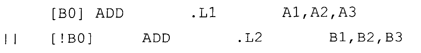
| Delay Slot and Functional Unit Latency Summary | |||||
| Instruction Type | Delay Slots | Function al Unit Latency | Read Cycles | Write Cycles ψ | Branch Taken ψ |
| NOP (no operation) | 0 | 1 | |||
| | 0 | 1 | i | i | |
| | 0 | 1 | i | i | |
| Two | 1 | 1 | i | i + 1 | |
| Multiply (16x16) | 1 | 1 | i | i + 1 | |
| Four | 3 | 1 | i | i + 3 | |
| | 4 | 1 | i | i, i + 4 | |
| | 5 | 1 | i | i + 5 |
| Fully Serial p-bit Pattern Execution | |
| Cycle | Instructions |
| 1 | A |
| 2 | B |
| 3 | C |
| 4 | D |
| 5 | E |
| 6 | F |
| 7 | G |
| 8 | H |
| Fully Parallel p-bit Pattern Execution | ||||||||
| Cycle | Instructions | |||||||
| 1 | A | B | C | D | E | F | G | H |
| Partially Serial p-bit Pattern Execution | |||
| Cycle | Instructions | ||
| 1 | A | ||
| 2 | B | ||
| 3 | C | D | E |
| 4 | F | G | H |
| instruction | A | |
| instruction | B | |
| instruction | C | |
| | | | instruction | D |
| | | | instruction | E |
| instruction | F | |
| | | | instruction | G |
| | | | instruction | H |
| Address Generator Options | ||
| Mode Field | Syntax | Modification Performed |
| 0 1 0 1 | *+R[ offsetR] | Positive offset; addr = base + offset * scale |
| 0 1 0 0 | *-R[ offsetR] | Negative offset; addr = base - offset * scale |
| 1 1 0 1 | *++R[ offsetR] | Preincrement; addr = base + offset * scale; base = addr |
| 1 1 0 0 | *--R[ offsetR] | Predecrement; addr = base - offset * scale; base = addr |
| 1 1 1 1 | *R++[ offsetR] | Postincrement; addr = base; base = base + offset * scale |
| 1 1 1 0 | *R--[offsetR] | Postdecrement; addr = base; base = base - offset * scale |
| 0 0 0 1 | *+R[ ucst5] | Positive offset; addr = base + offset * scale |
| 0 0 0 0 | *-R[ ucst5] | Negative offset; addr = base - offset * scale |
| 1 0 0 1 | *++R[ ucst5] | Preincrement; addr = base + offset * scale; base = addr |
| 1 0 0 0 | *- -R[ ucst5] | Predecrement; addr = base - offset * scale; base = addr |
| 1 0 1 1 | *R++[ ucst5] | Postincrement; addr = base; base = base + offset * scale |
| 1 0 1 0 | *R- -[ ucst5] | Postdecrement; addr = base; base = base - offset * scale |
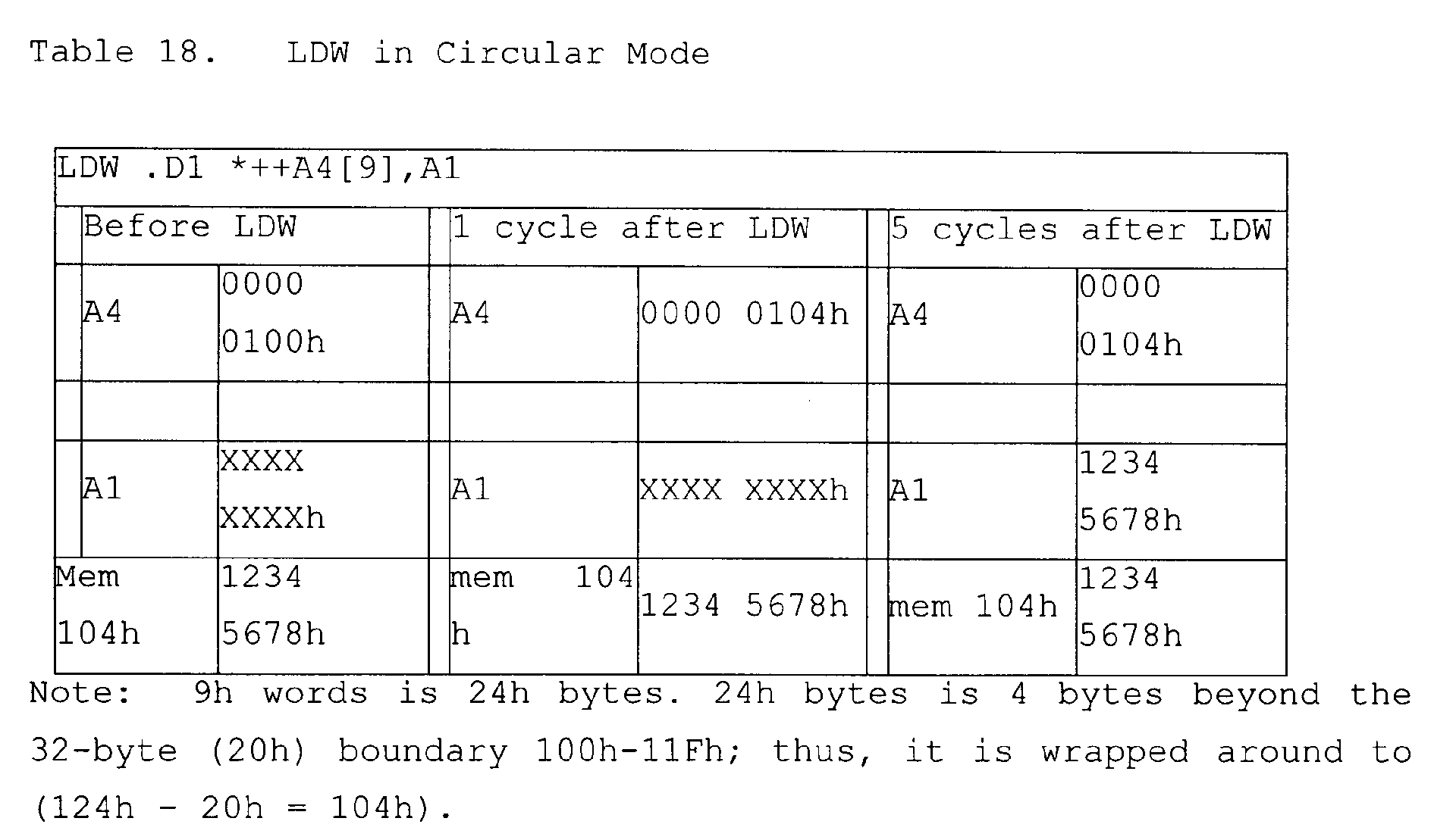
| ADDAH in Circular Mode | ||||
| ADDAH .D1 A4,A1,A4 | ||||
| Before | 1 cycle after ADDAH | |||
| A4 | 0000 0100h | A4 | 0000 0106h | |
| A1 | 0000 0013h | A1 | 0000 0013h |

| Pipeline Phase Description | ||||
| Pipeline | Pipeline Phase | Symb ol | During This Phase | Instruction Types Completed |
| Program Fetch | Program Address Generate | PG | Address of the fetch packet is determined. | |
| Program Address Send | PS | Address of fetch packet is sent to memory. | ||
| Program Wait | PW | Program memory access is performed. | ||
| Program Data Receive | PR | Fetch packet is expected at CPU boundary. | ||
| Program Decode | Dispatch | DP | Next execute packet in fetch packet determined and sent to the appropriate functional units to be decoded. | |
| Decode | DC | Instructions are decoded at functional units. | ||
| Execute | Execute 1 | E1 | For all instruction types, conditions for instructions are evaluated and operands read. Load and store instructions: address generation is computed and address modifications written to register file Branch instructions: affects branch fetch packet in PG | Single-cycle |
| phase Single-cycle instructions: results are written to a register file | ||||
| Execute 2 | E2 | Load instructions: address is sent to memory Store instructions and STP: address and data are sent to memory Single-cycle instructions that saturate results set the SAT bit in the Control Status Register (CSR) if saturation occurs. Multiply instructions: results are written to a register file | Stores STP Multiplies | |
| Execute 3 | E3 | Data memory accesses are performed. Any multiply instruction that saturates results sets the SAT bit in the Control Status Register (CSR) if saturation occurs. | ||
| Execute 4 | E4 | Load instructions: data is brought to CPU boundary | ||
| Execute 5 | E5 | Load instructions: data is loaded into register | Loads |
| Delay Slot Summary | ||
| Instruction Type | Delay Slots | Execute Stages Used |
| Branch (The cycle when the target enters E1) | 5 | E1-branch target E1 |
| Load (LD) (Incoming Data) | 4 | E1 - E5 |
| Load (LD) (Address Modification) | 0 | E1 |
| Multiply | 1 | E1 - E2 |
| Single- | 0 | |
| Store | ||
| 0 | E1 | |
| NOP (no execution pipeline operation) | - | - |
| STP (no CPU internal results written) | - | - |
| Program and Data Cache Fields | ||||
| Bit Field Counter | Program Cache (PCC) | Data Cache Control (DCC) | Mode Name | Description |
| 000 | PCM | DCM | Cache mapped | Cache mapped into memory. Cache not updated. Cache not accessed (except as mapped into memory). Tags can either be invalidated automatically or invalidated by preceding or following flush (depending on cache implementation). |
| 001 | PCFL | DCFL | Cache flush | Entire cache invalidated. Cache bypassed for accesses. Cache not updated on accesses. |
| 010 | PCE | DCE | Cache enable | Cache accessed. Cache updated. |
| 011 | PCFR | DCFR | Cache freeze | Cache accessed on reads. Cache not updated on reads. Whether the cache is updated or invalidated on writes depends on the specific device. |
| 100 | PCB | DCB | Cache bypass | Cache not accessed. Cache not updated on reads. Write action is the same as for cache freeze. |
| | Reserved | Reserved | ||
| 110 | Reserved | Reserved | ||
| 111 | Reserved | Reserved |
| Instruction for Operating Directly on Packed Data | ||
| Operation | Quad 8-bit | Paired 16-bit |
| Multiply | X | X |
| Multiply with Saturation | X | |
| Addition/Subtraction | X | X * |
| Addition with Saturation | X | X |
| Absolute Value | X | |
| Subtract with Absolute Value | X | |
| Compare | X | X |
| Shift | X | |
| Data Pack/Unpack | X | X |
| Data Pack with Saturation | X | X |
| Dot product with optional negate | X | X |
| Min/Max/Average | X | X |
| Bit-expansion (Mask generation) | X | X |


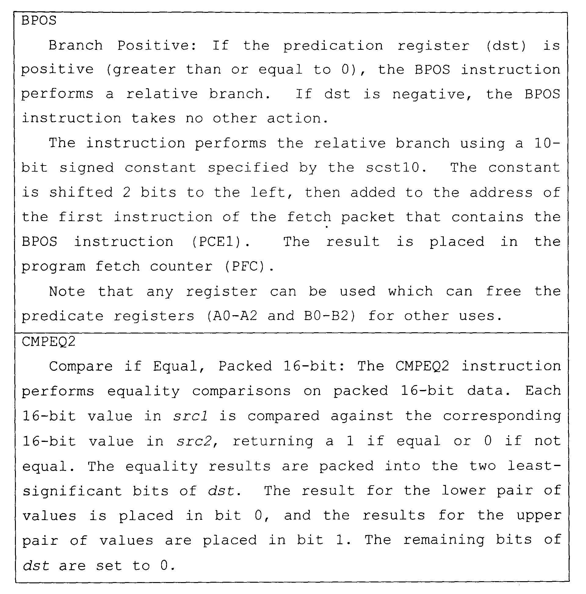


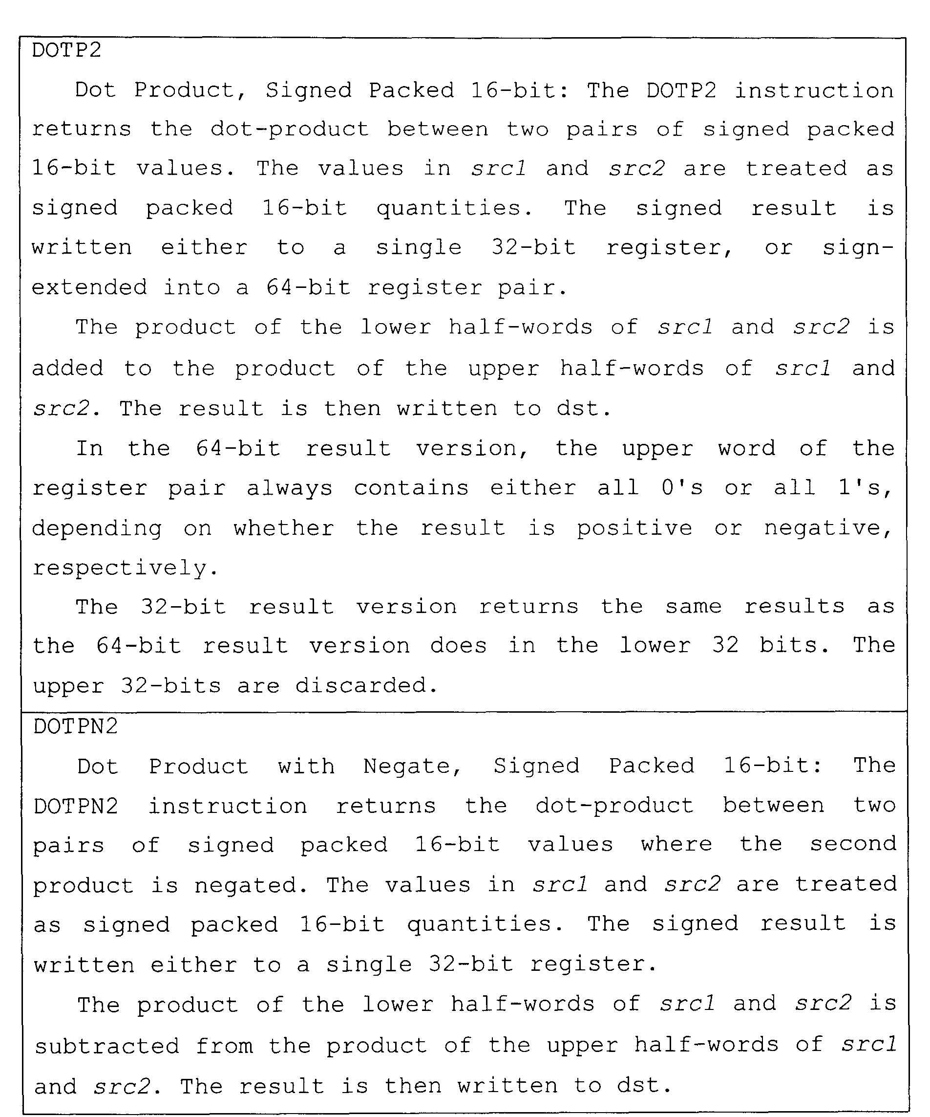


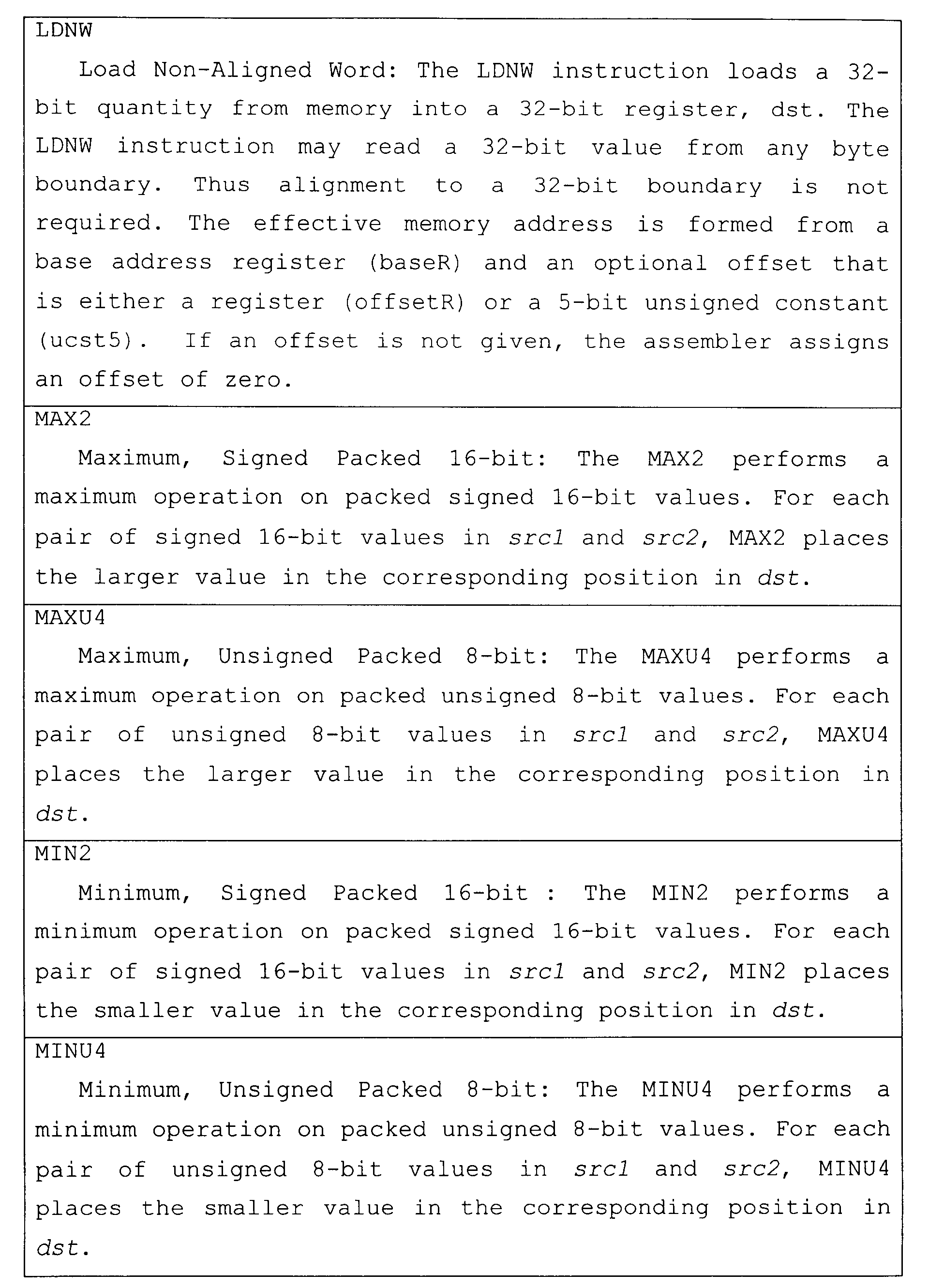

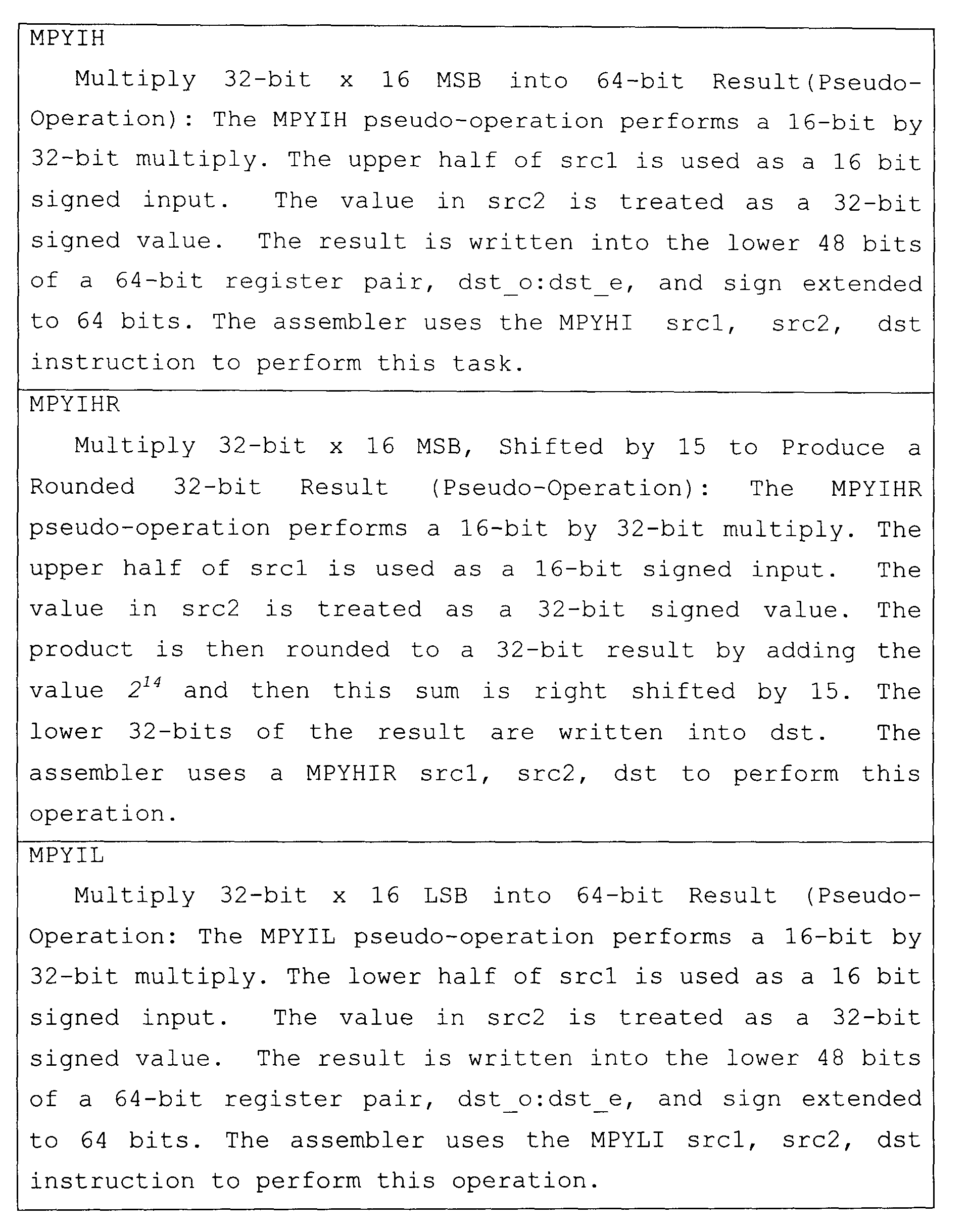


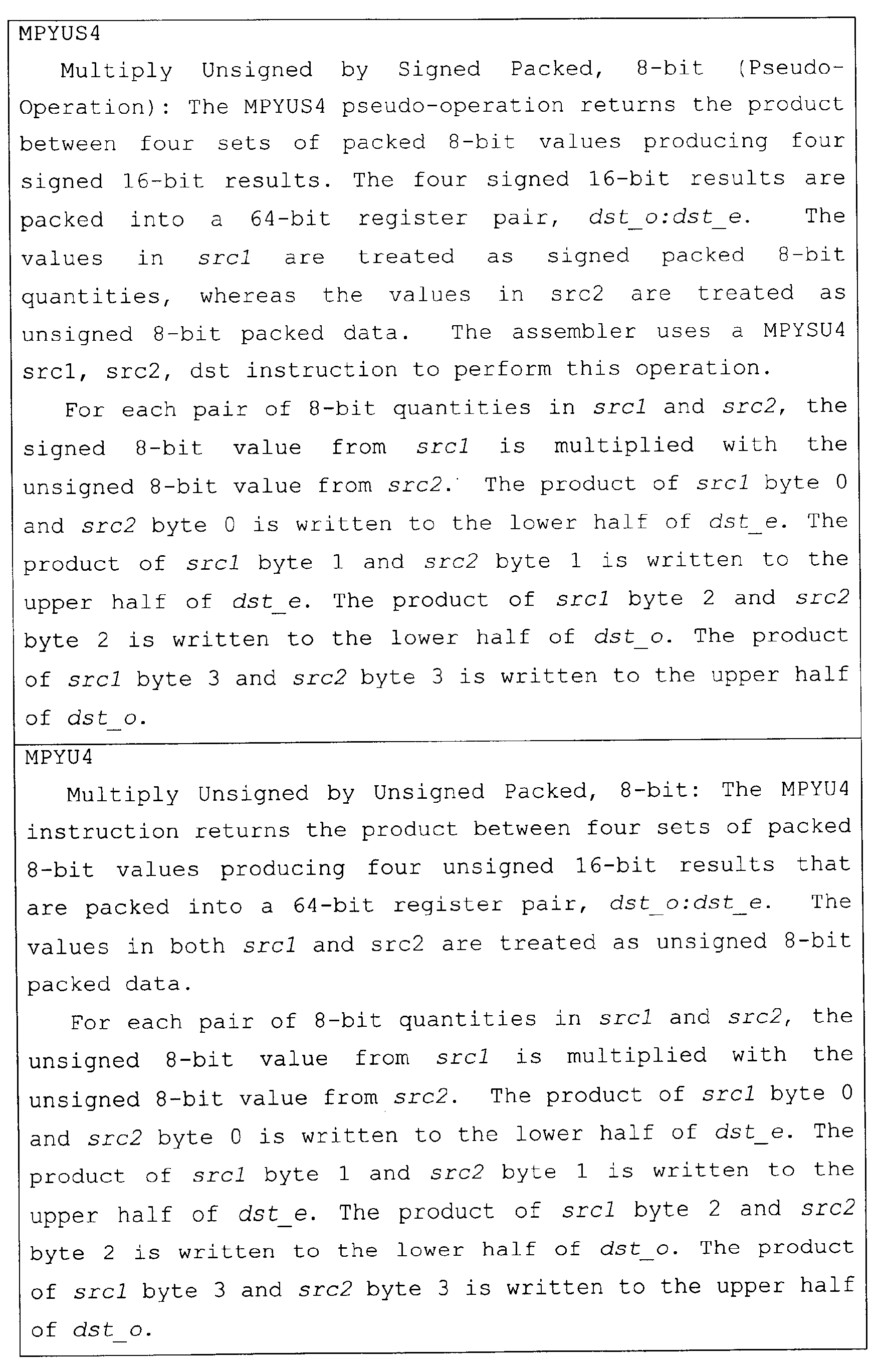
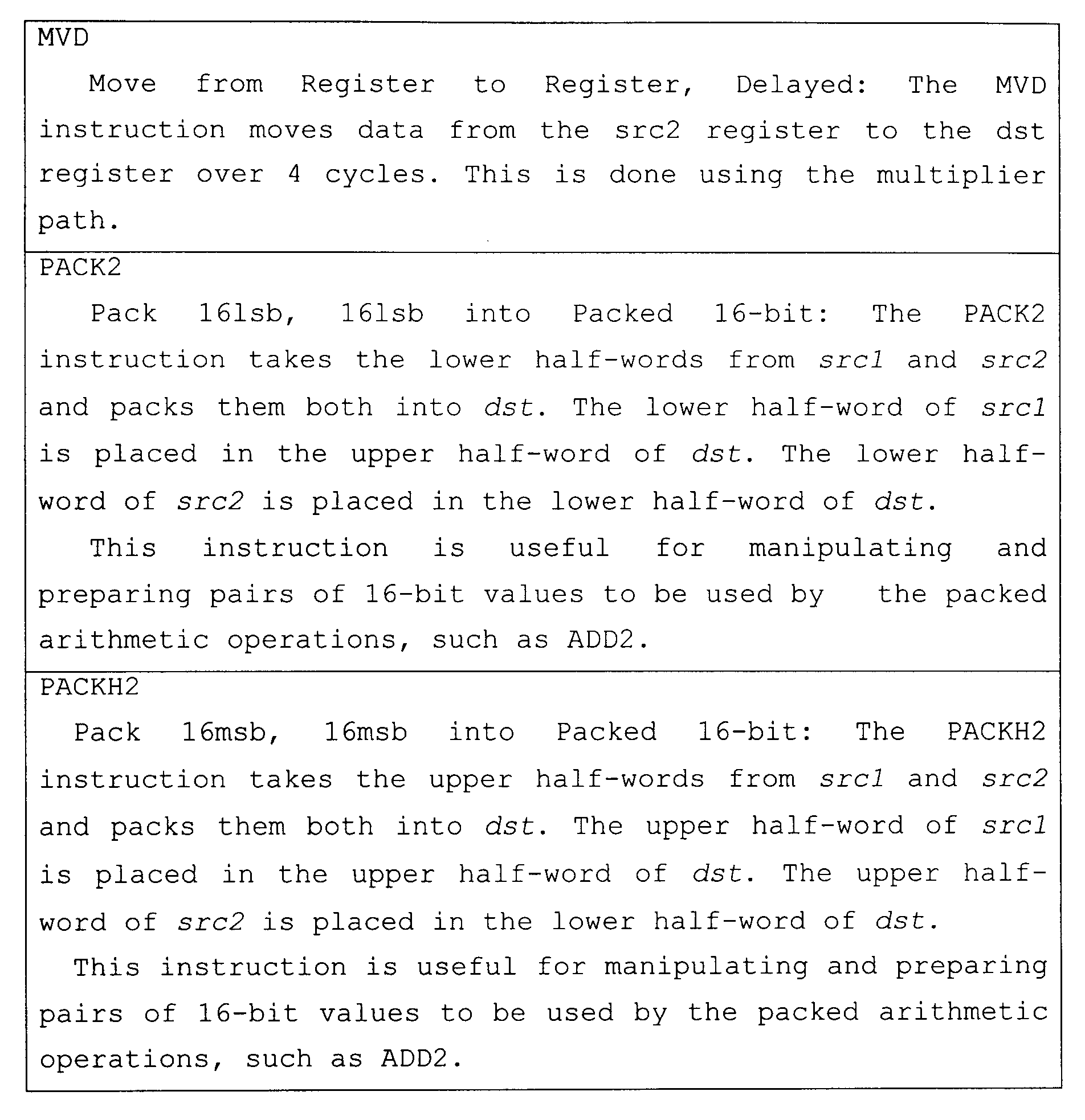

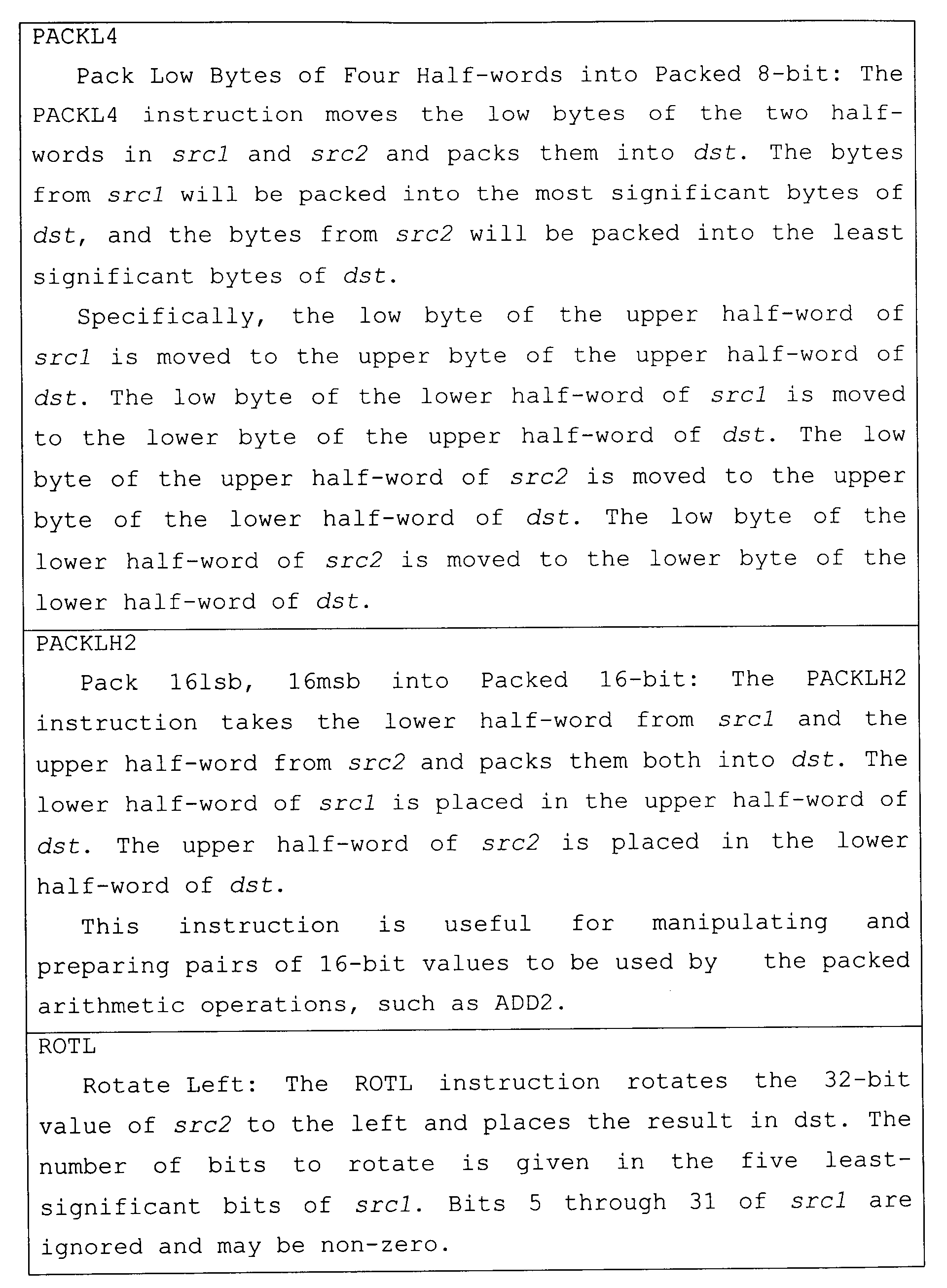


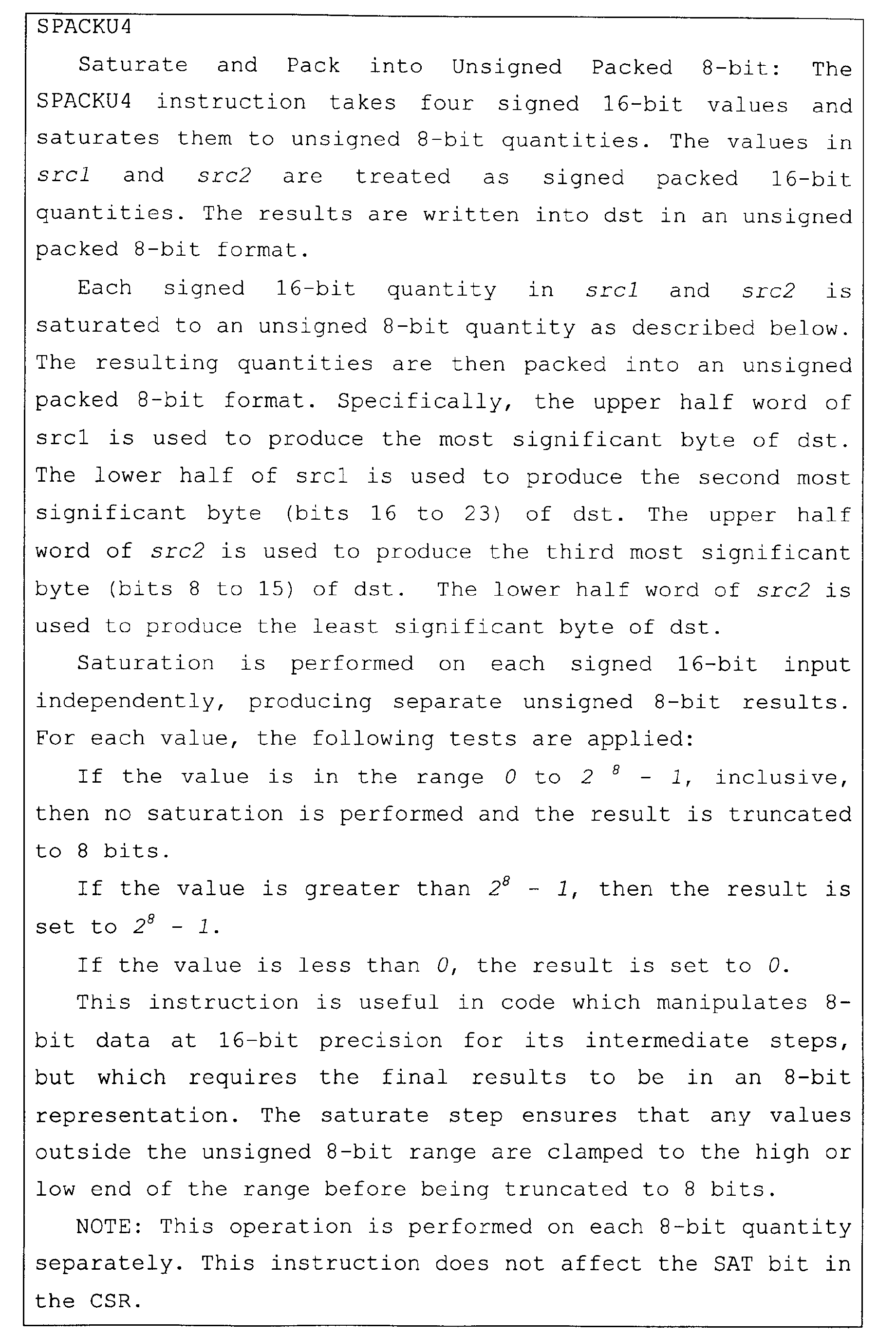
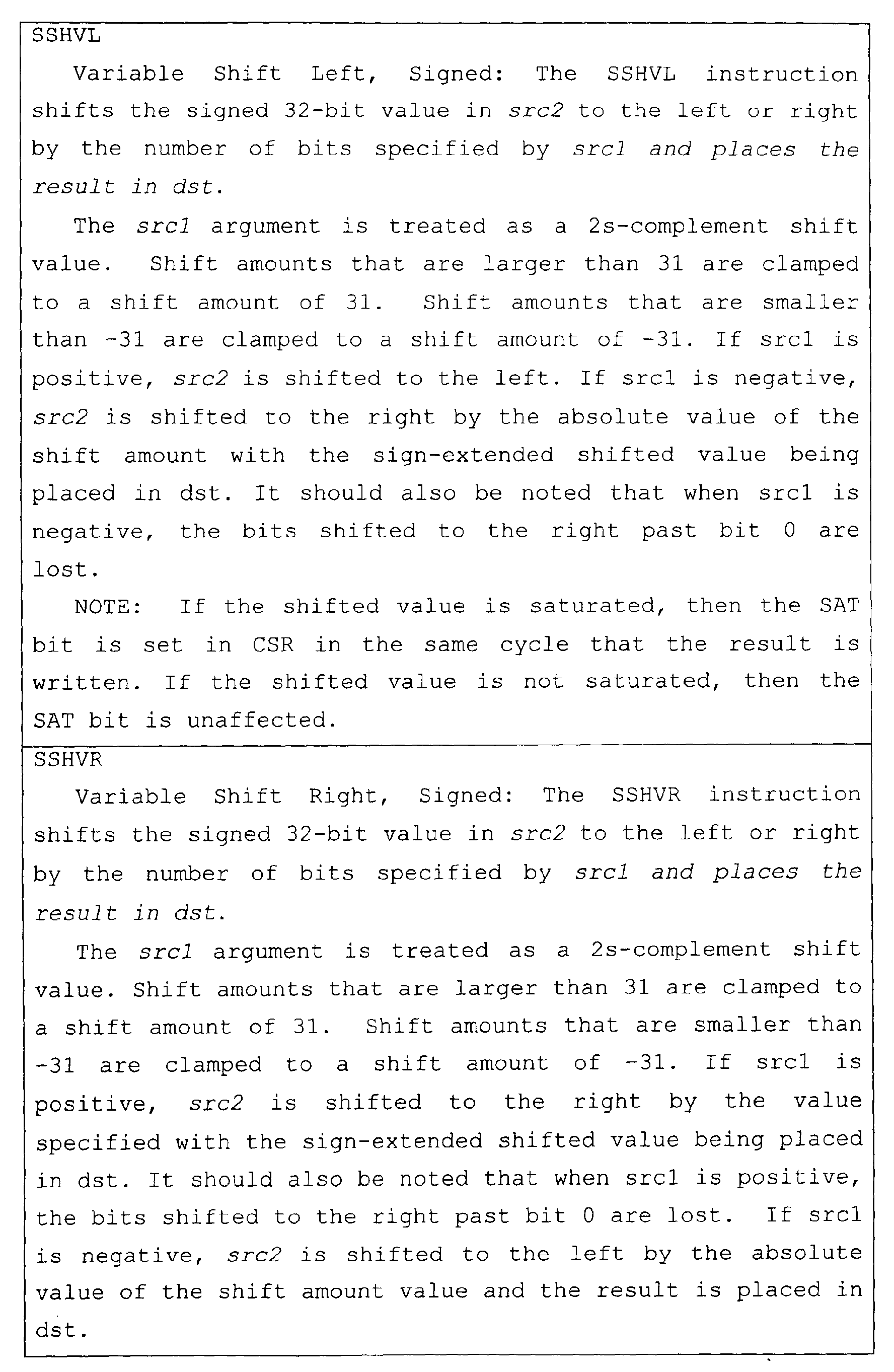


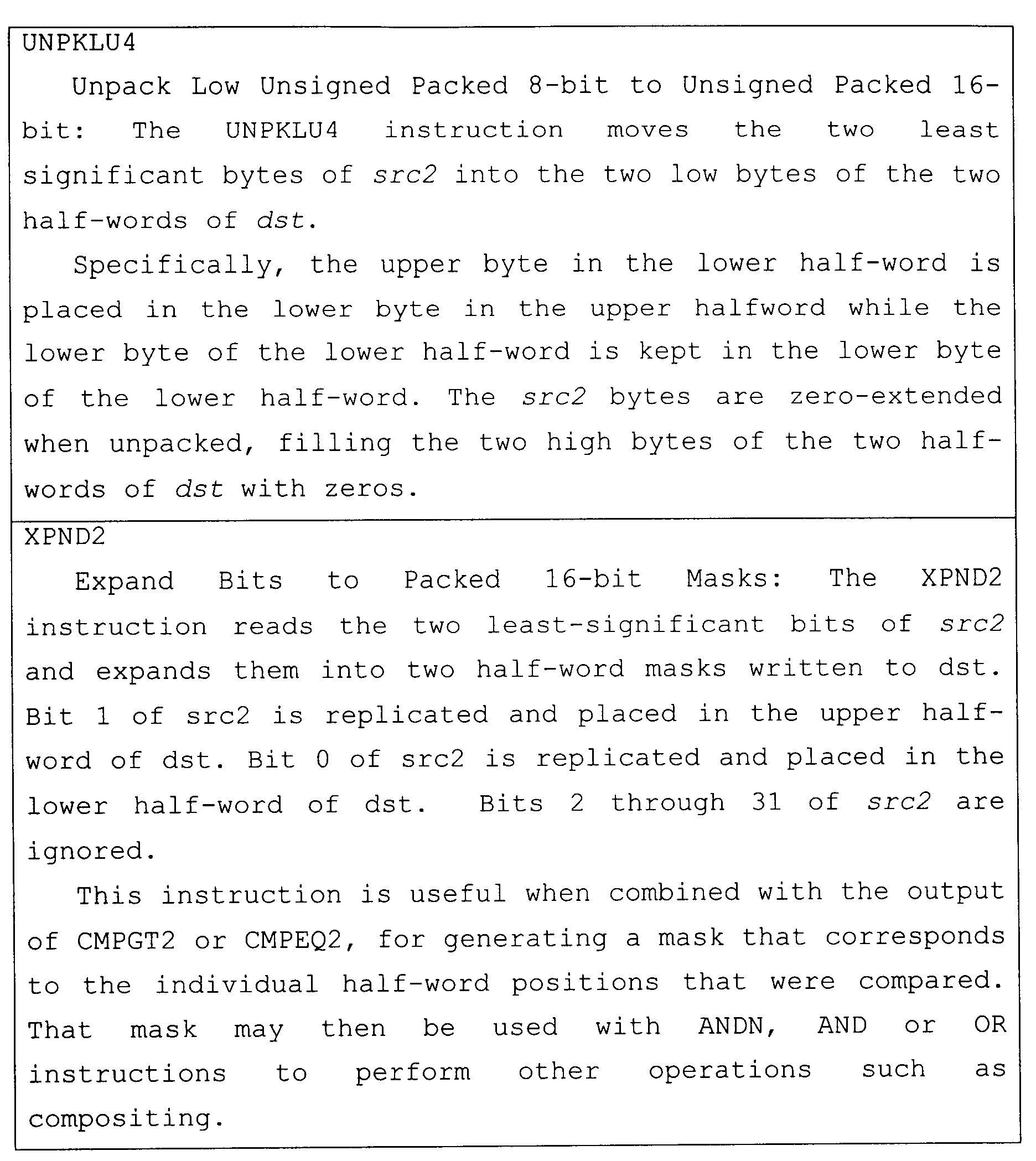
- VLIW
- Software Pipelining
- High level Vector Optimizations to transform the code
- Non-aligned memory accesses
- Split-ALU operations


Claims (10)
- A microprocessor having an instruction execution pipeline with a plurality of pipeline phases, comprising:program fetch circuitry operable to fetch instructions;instruction decode circuitry connected to receive fetched instructions from the program fetch circuitry, the instruction decode circuitry operable to decode a set of single instruction, multiple data (SIMD) instructions; andat least a first functional unit connected to receive control signals from the instruction decode circuitry, wherein the first functional unit comprises:multi-field arithmetic/logic unit (ALU) circuitry connected to receive a plurality of source operands and having outputs connected to provide a multi-field result as a destination operand in response to control signals from the instruction decode circuitry, wherein the multi-field ALU circuitry is operable to treat the plurality of source operands as a set of N1 fields, such that the multi-field result includes N1 results corresponding to the set of N1 fields; andwherein the first functional unit is operable to provide the multi-field result in response to a single SIMD instruction of a first type.
- The microprocessor of claim 1, further comprising a second functional unit connected to operate in parallel with the first functional unit, wherein the second functional unit comprises multi-field multiplication circuitry connected to receive a plurality of source operands and having outputs connected to provide a multi-field result as a destination operand in response to control signals from the instruction decode circuitry, wherein the multi-field multiplication circuitry is operable to treat the plurality of source operands as a set of N2 fields, such that the multi-field result includes N2 results corresponding to the set of N2 fields; and
wherein the second functional unit is operable to provide the multi-field result in response to a single SIMD instruction of a second type. - The microprocessor of claim 1 or claim 2, further comprising:at least a first load/store unit connected to at least a first storage register of the microprocessor;a memory subsystem having at least a first memory port connected to the first load/store unit;address generation circuitry in the first load/store unit having a first address output connected to the first memory port, the address generation circuitry operable to provide a first byte address on the first address output;an extraction circuit connected to the first memory port, wherein the extraction circuit is operable to provide a first non-aligned multi-byte data item to the first load/store unit responsive to the first byte address; and wherein the load/store unit is operable to provide the multi-byte data item in response to a single instruction of a third type.
- The microprocessor of claim 3, wherein the first storage register is part of a register file connected to the first functional unit and to the second functional unit for providing the plurality of source operands and connected to the first functional unit and to the second function unit to receive the destination operands.
- The microprocessor of Claim 3 or claim 4, wherein the instructions of the first type, second type and third type all have a field for identifying a predicate register.
- A digital system including a microprocessor as claimed in any one of claims 1 to 5.
- A digital system as claimed in claim 6, which is a cellular telephone, further comprising:an integrated keyboard connected to the microprocessor via a keyboard adapter;a display, connected to the microprocessor via a display adapter;radio frequency (RF) circuitry connected to the microprocessor; andan aerial connected to the RF circuitry.
- A method of operating a microprocessor, comprising the steps of:providing multi-field arithmetic/logic unit (ALU) circuitry for operating on a set of source operands to form a multi-field destination operand by treating the plurality of source operands as a set of N1 fields, such that the multi-field result includes N1 results corresponding to the set of N1 fields; andproviding a set of single instruction, multiple data (SIMD) instructions to direct the operation of the multi-field ALU circuitry.
- A method of operating a microprocessor, comprising the steps of:providing multi-field arithmetic/logic unit (ALU) circuitry for operating on a set of source operands to form a multi-field destination operand by treating the plurality of source operands as a set of N1 fields, such that the multi-field result includes N1 results corresponding to the set of N1 fields;providing multi-field multiplication circuitry for operating on a set of source operands to form a multi-field destination operand by treating the plurality of source operands as a set of N2 fields, such that the multi-field result includes N2 results corresponding to the set of N2 fields; andproviding a set of single instruction, multiple data (SIMD) instructions to direct the operation of the multi-field ALU circuitry and the multi-field multiplication circuitry.
- The method of claim 8 or claim 9, further comprising the step of providing load/store circuitry operable to transfer a multi-byte data item to a memory circuit at a byte address that is not word aligned.
Applications Claiming Priority (4)
| Application Number | Priority Date | Filing Date | Title |
|---|---|---|---|
| US16551299P | 1999-11-15 | 1999-11-15 | |
| US165512P | 1999-11-15 | ||
| US18352700P | 2000-02-18 | 2000-02-18 | |
| US183527P | 2000-02-18 |
Publications (2)
| Publication Number | Publication Date |
|---|---|
| EP1102163A2 true EP1102163A2 (en) | 2001-05-23 |
| EP1102163A3 EP1102163A3 (en) | 2005-06-29 |
Family
ID=26861452
Family Applications (1)
| Application Number | Title | Priority Date | Filing Date |
|---|---|---|---|
| EP00310098A Withdrawn EP1102163A3 (en) | 1999-11-15 | 2000-11-14 | Microprocessor with improved instruction set architecture |
Country Status (4)
| Country | Link |
|---|---|
| EP (1) | EP1102163A3 (en) |
| JP (2) | JP2001202245A (en) |
| CN (1) | CN1194292C (en) |
| TW (1) | TW543000B (en) |
Cited By (20)
| Publication number | Priority date | Publication date | Assignee | Title |
|---|---|---|---|---|
| GB2367659A (en) * | 2000-10-04 | 2002-04-10 | Advanced Risc Mach Ltd | SIMD saturation instruction with variable bit length |
| US8484441B2 (en) | 2004-03-31 | 2013-07-09 | Icera Inc. | Apparatus and method for separate asymmetric control processing and data path processing in a configurable dual path processor that supports instructions having different bit widths |
| US8510534B2 (en) | 2002-05-24 | 2013-08-13 | St-Ericsson Sa | Scalar/vector processor that includes a functional unit with a vector section and a scalar section |
| US9477475B2 (en) | 2004-03-31 | 2016-10-25 | Nvidia Technology Uk Limited | Apparatus and method for asymmetric dual path processing |
| US9720693B2 (en) | 2015-06-26 | 2017-08-01 | Microsoft Technology Licensing, Llc | Bulk allocation of instruction blocks to a processor instruction window |
| US9792252B2 (en) | 2013-05-31 | 2017-10-17 | Microsoft Technology Licensing, Llc | Incorporating a spatial array into one or more programmable processor cores |
| US9946548B2 (en) | 2015-06-26 | 2018-04-17 | Microsoft Technology Licensing, Llc | Age-based management of instruction blocks in a processor instruction window |
| US9952867B2 (en) | 2015-06-26 | 2018-04-24 | Microsoft Technology Licensing, Llc | Mapping instruction blocks based on block size |
| US10101998B2 (en) | 2013-01-23 | 2018-10-16 | International Business Machines Corporation | Vector checksum instruction |
| US10146534B2 (en) | 2013-01-23 | 2018-12-04 | International Business Machines Corporation | Vector Galois field multiply sum and accumulate instruction |
| US10169044B2 (en) | 2015-06-26 | 2019-01-01 | Microsoft Technology Licensing, Llc | Processing an encoding format field to interpret header information regarding a group of instructions |
| US10175988B2 (en) | 2015-06-26 | 2019-01-08 | Microsoft Technology Licensing, Llc | Explicit instruction scheduler state information for a processor |
| US10191747B2 (en) | 2015-06-26 | 2019-01-29 | Microsoft Technology Licensing, Llc | Locking operand values for groups of instructions executed atomically |
| US10203956B2 (en) | 2013-01-23 | 2019-02-12 | International Business Machines Corporation | Vector floating point test data class immediate instruction |
| US10346168B2 (en) | 2015-06-26 | 2019-07-09 | Microsoft Technology Licensing, Llc | Decoupled processor instruction window and operand buffer |
| US10409599B2 (en) | 2015-06-26 | 2019-09-10 | Microsoft Technology Licensing, Llc | Decoding information about a group of instructions including a size of the group of instructions |
| US10409606B2 (en) | 2015-06-26 | 2019-09-10 | Microsoft Technology Licensing, Llc | Verifying branch targets |
| CN113032012A (en) * | 2015-04-04 | 2021-06-25 | 德州仪器公司 | Apparatus for low energy accelerator processor architecture |
| CN115904501A (en) * | 2016-12-20 | 2023-04-04 | 德克萨斯仪器股份有限公司 | Stream engine with multi-dimensional circular addressing selectable in each dimension |
| CN119252304A (en) * | 2021-04-07 | 2025-01-03 | 华为技术有限公司 | Storage device and method for processing data |
Families Citing this family (21)
| Publication number | Priority date | Publication date | Assignee | Title |
|---|---|---|---|---|
| JP4545777B2 (en) * | 2002-06-28 | 2010-09-15 | ルネサスエレクトロニクス株式会社 | Data processing device |
| CN107832241B (en) * | 2003-04-11 | 2021-10-08 | 富意科技公司 | Integrated circuit storage device or method capable of realizing automatic operation |
| US7949856B2 (en) | 2004-03-31 | 2011-05-24 | Icera Inc. | Method and apparatus for separate control processing and data path processing in a dual path processor with a shared load/store unit |
| CN100440812C (en) * | 2004-04-23 | 2008-12-03 | 华为技术有限公司 | Device and method for implementing incentive message and test method for digital circuit logic simulation |
| US7496729B2 (en) * | 2004-05-13 | 2009-02-24 | International Business Machines Corporation | Method and apparatus to eliminate interpartition covert storage channel and partition analysis |
| JP2007048019A (en) * | 2005-08-10 | 2007-02-22 | Sony Computer Entertainment Inc | Emulation method, emulator, computer embedded device, and program for emulator |
| JP2009048532A (en) * | 2007-08-22 | 2009-03-05 | Nec Electronics Corp | Microprocessor |
| JP2009075676A (en) | 2007-09-18 | 2009-04-09 | Nec Electronics Corp | Microprocessor |
| CN101667114B (en) * | 2009-09-30 | 2012-07-04 | 西安电子科技大学 | Overlong instruction set microprocessing system suitable for matrix inversion |
| US9552206B2 (en) * | 2010-11-18 | 2017-01-24 | Texas Instruments Incorporated | Integrated circuit with control node circuitry and processing circuitry |
| JP5853177B2 (en) * | 2011-04-08 | 2016-02-09 | パナソニックIpマネジメント株式会社 | Data processing apparatus and data processing method |
| EP3093758B1 (en) * | 2013-03-15 | 2020-06-24 | Oracle International Corporation | Run length instruction for single instruction multiple data processors |
| US9219499B2 (en) * | 2014-05-16 | 2015-12-22 | Robert Bosch Gmbh | Run time compression method for a vehicle communication bus |
| GB2548908B (en) * | 2016-04-01 | 2019-01-30 | Advanced Risc Mach Ltd | Complex multiply instruction |
| US10067744B2 (en) | 2016-12-08 | 2018-09-04 | International Business Machines Corporation | Overflow detection for sign-magnitude adders |
| CN106886680A (en) * | 2017-02-09 | 2017-06-23 | 无锡科美达医疗科技有限公司 | A kind of ultrasonic remote real-time consultation system |
| CN111105033B (en) * | 2017-12-14 | 2024-01-12 | 中科寒武纪科技股份有限公司 | Neural network processor board card and related products |
| CN109189475B (en) * | 2018-08-16 | 2022-06-10 | 北京算能科技有限公司 | Method for constructing instruction set of programmable artificial intelligence accelerator |
| US11270196B2 (en) | 2019-10-15 | 2022-03-08 | International Business Machines Corporation | Multi-mode low-precision inner-product computation circuits for massively parallel neural inference engine |
| CN111124496B (en) * | 2019-12-25 | 2022-06-21 | 合肥中感微电子有限公司 | Multi-cycle instruction processing method, processor and electronic equipment |
| CN114331803B (en) * | 2021-12-24 | 2025-04-01 | 浙江大学 | A highly energy-efficient dedicated processor for multi-level digital halftoning |
Family Cites Families (3)
| Publication number | Priority date | Publication date | Assignee | Title |
|---|---|---|---|---|
| US5327579A (en) * | 1990-11-06 | 1994-07-05 | Nippon Telegraph And Telephone Corporation | Scanning systems using tree structures |
| EP0973099A3 (en) * | 1994-09-13 | 2003-04-16 | Lockheed Martin Corporation | Parallel data processor |
| JPH11308574A (en) * | 1998-04-22 | 1999-11-05 | Sony Corp | Scanning line number conversion apparatus and method |
-
2000
- 2000-11-14 EP EP00310098A patent/EP1102163A3/en not_active Withdrawn
- 2000-11-15 JP JP2000403992A patent/JP2001202245A/en active Pending
- 2000-11-15 TW TW089124170A patent/TW543000B/en not_active IP Right Cessation
- 2000-11-15 CN CN00133915.XA patent/CN1194292C/en not_active Expired - Fee Related
- 2000-11-15 JP JP2000348735A patent/JP2001256038A/en active Pending
Cited By (25)
| Publication number | Priority date | Publication date | Assignee | Title |
|---|---|---|---|---|
| GB2367659A (en) * | 2000-10-04 | 2002-04-10 | Advanced Risc Mach Ltd | SIMD saturation instruction with variable bit length |
| US8510534B2 (en) | 2002-05-24 | 2013-08-13 | St-Ericsson Sa | Scalar/vector processor that includes a functional unit with a vector section and a scalar section |
| US9477475B2 (en) | 2004-03-31 | 2016-10-25 | Nvidia Technology Uk Limited | Apparatus and method for asymmetric dual path processing |
| US8484441B2 (en) | 2004-03-31 | 2013-07-09 | Icera Inc. | Apparatus and method for separate asymmetric control processing and data path processing in a configurable dual path processor that supports instructions having different bit widths |
| US10338918B2 (en) | 2013-01-23 | 2019-07-02 | International Business Machines Corporation | Vector Galois Field Multiply Sum and Accumulate instruction |
| US10101998B2 (en) | 2013-01-23 | 2018-10-16 | International Business Machines Corporation | Vector checksum instruction |
| US10146534B2 (en) | 2013-01-23 | 2018-12-04 | International Business Machines Corporation | Vector Galois field multiply sum and accumulate instruction |
| US10877753B2 (en) | 2013-01-23 | 2020-12-29 | International Business Machines Corporation | Vector galois field multiply sum and accumulate instruction |
| US10671389B2 (en) | 2013-01-23 | 2020-06-02 | International Business Machines Corporation | Vector floating point test data class immediate instruction |
| US10606589B2 (en) | 2013-01-23 | 2020-03-31 | International Business Machines Corporation | Vector checksum instruction |
| US10203956B2 (en) | 2013-01-23 | 2019-02-12 | International Business Machines Corporation | Vector floating point test data class immediate instruction |
| US9792252B2 (en) | 2013-05-31 | 2017-10-17 | Microsoft Technology Licensing, Llc | Incorporating a spatial array into one or more programmable processor cores |
| CN113032012B (en) * | 2015-04-04 | 2023-08-15 | 德州仪器公司 | Apparatus for low energy accelerator processor architecture |
| CN113032012A (en) * | 2015-04-04 | 2021-06-25 | 德州仪器公司 | Apparatus for low energy accelerator processor architecture |
| US9946548B2 (en) | 2015-06-26 | 2018-04-17 | Microsoft Technology Licensing, Llc | Age-based management of instruction blocks in a processor instruction window |
| US10346168B2 (en) | 2015-06-26 | 2019-07-09 | Microsoft Technology Licensing, Llc | Decoupled processor instruction window and operand buffer |
| US10409599B2 (en) | 2015-06-26 | 2019-09-10 | Microsoft Technology Licensing, Llc | Decoding information about a group of instructions including a size of the group of instructions |
| US10409606B2 (en) | 2015-06-26 | 2019-09-10 | Microsoft Technology Licensing, Llc | Verifying branch targets |
| US10191747B2 (en) | 2015-06-26 | 2019-01-29 | Microsoft Technology Licensing, Llc | Locking operand values for groups of instructions executed atomically |
| US10175988B2 (en) | 2015-06-26 | 2019-01-08 | Microsoft Technology Licensing, Llc | Explicit instruction scheduler state information for a processor |
| US10169044B2 (en) | 2015-06-26 | 2019-01-01 | Microsoft Technology Licensing, Llc | Processing an encoding format field to interpret header information regarding a group of instructions |
| US9952867B2 (en) | 2015-06-26 | 2018-04-24 | Microsoft Technology Licensing, Llc | Mapping instruction blocks based on block size |
| US9720693B2 (en) | 2015-06-26 | 2017-08-01 | Microsoft Technology Licensing, Llc | Bulk allocation of instruction blocks to a processor instruction window |
| CN115904501A (en) * | 2016-12-20 | 2023-04-04 | 德克萨斯仪器股份有限公司 | Stream engine with multi-dimensional circular addressing selectable in each dimension |
| CN119252304A (en) * | 2021-04-07 | 2025-01-03 | 华为技术有限公司 | Storage device and method for processing data |
Also Published As
| Publication number | Publication date |
|---|---|
| JP2001202245A (en) | 2001-07-27 |
| CN1309347A (en) | 2001-08-22 |
| JP2001256038A (en) | 2001-09-21 |
| EP1102163A3 (en) | 2005-06-29 |
| TW543000B (en) | 2003-07-21 |
| CN1194292C (en) | 2005-03-23 |
Similar Documents
| Publication | Publication Date | Title |
|---|---|---|
| EP1102163A2 (en) | Microprocessor with improved instruction set architecture | |
| US7062526B1 (en) | Microprocessor with rounding multiply instructions | |
| US6745319B1 (en) | Microprocessor with instructions for shuffling and dealing data | |
| US6539467B1 (en) | Microprocessor with non-aligned memory access | |
| US6671797B1 (en) | Microprocessor with expand instruction for forming a mask from one bit | |
| US6748521B1 (en) | Microprocessor with instruction for saturating and packing data | |
| US6711602B1 (en) | Data processor with flexible multiply unit | |
| US8510534B2 (en) | Scalar/vector processor that includes a functional unit with a vector section and a scalar section | |
| US7937559B1 (en) | System and method for generating a configurable processor supporting a user-defined plurality of instruction sizes | |
| US6058465A (en) | Single-instruction-multiple-data processing in a multimedia signal processor | |
| US5838984A (en) | Single-instruction-multiple-data processing using multiple banks of vector registers | |
| CN113032012B (en) | Apparatus for low energy accelerator processor architecture | |
| US6574724B1 (en) | Microprocessor with non-aligned scaled and unscaled addressing | |
| US7487338B2 (en) | Data processor for modifying and executing operation of instruction code according to the indication of other instruction code | |
| US6453405B1 (en) | Microprocessor with non-aligned circular addressing | |
| EP1124181B1 (en) | Data processing apparatus | |
| US20030061471A1 (en) | Data processor | |
| US6484253B1 (en) | Data processor | |
| JPH0766324B2 (en) | Data processing device | |
| US20050188182A1 (en) | Microprocessor having a set of byte intermingling instructions | |
| CN108139911A (en) | Conditional Execution Specifications for Instructions Using Conditional Expansion Slots in the Same Execution Package of a VLIW Processor | |
| US5924114A (en) | Circular buffer with two different step sizes | |
| US6757819B1 (en) | Microprocessor with instructions for shifting data responsive to a signed count value | |
| JP2004005603A (en) | Method and device for performing repeated block instruction by zero cycle overhead along nested loop | |
| US6889320B1 (en) | Microprocessor with an instruction immediately next to a branch instruction for adding a constant to a program counter |
Legal Events
| Date | Code | Title | Description |
|---|---|---|---|
| PUAI | Public reference made under article 153(3) epc to a published international application that has entered the european phase |
Free format text: ORIGINAL CODE: 0009012 |
|
| AK | Designated contracting states |
Kind code of ref document: A2 Designated state(s): AT BE CH CY DE DK ES FI FR GB GR IE IT LI LU MC NL PT SE TR |
|
| AX | Request for extension of the european patent |
Free format text: AL;LT;LV;MK;RO;SI |
|
| PUAL | Search report despatched |
Free format text: ORIGINAL CODE: 0009013 |
|
| AK | Designated contracting states |
Kind code of ref document: A3 Designated state(s): AT BE CH CY DE DK ES FI FR GB GR IE IT LI LU MC NL PT SE TR |
|
| AX | Request for extension of the european patent |
Extension state: AL LT LV MK RO SI |
|
| RIC1 | Information provided on ipc code assigned before grant |
Ipc: 7G 06F 9/302 B Ipc: 7G 06F 15/80 A |
|
| STAA | Information on the status of an ep patent application or granted ep patent |
Free format text: STATUS: THE APPLICATION HAS BEEN WITHDRAWN |
|
| 17P | Request for examination filed |
Effective date: 20051229 |
|
| 18W | Application withdrawn |
Effective date: 20060116 |