EP0845837A2 - Connector comprising stacked modules for chip cards - Google Patents
Connector comprising stacked modules for chip cards Download PDFInfo
- Publication number
- EP0845837A2 EP0845837A2 EP97120219A EP97120219A EP0845837A2 EP 0845837 A2 EP0845837 A2 EP 0845837A2 EP 97120219 A EP97120219 A EP 97120219A EP 97120219 A EP97120219 A EP 97120219A EP 0845837 A2 EP0845837 A2 EP 0845837A2
- Authority
- EP
- European Patent Office
- Prior art keywords
- connector
- sub
- plug
- face
- card
- Prior art date
- Legal status (The legal status is an assumption and is not a legal conclusion. Google has not performed a legal analysis and makes no representation as to the accuracy of the status listed.)
- Granted
Links
Images


Classifications
-
- G—PHYSICS
- G06—COMPUTING OR CALCULATING; COUNTING
- G06K—GRAPHICAL DATA READING; PRESENTATION OF DATA; RECORD CARRIERS; HANDLING RECORD CARRIERS
- G06K7/00—Methods or arrangements for sensing record carriers, e.g. for reading patterns
- G06K7/0013—Methods or arrangements for sensing record carriers, e.g. for reading patterns by galvanic contacts, e.g. card connectors for ISO-7816 compliant smart cards or memory cards, e.g. SD card readers
- G06K7/0034—Methods or arrangements for sensing record carriers, e.g. for reading patterns by galvanic contacts, e.g. card connectors for ISO-7816 compliant smart cards or memory cards, e.g. SD card readers the connector being capable of simultaneously receiving a plurality of cards in the same insertion slot
-
- G—PHYSICS
- G06—COMPUTING OR CALCULATING; COUNTING
- G06K—GRAPHICAL DATA READING; PRESENTATION OF DATA; RECORD CARRIERS; HANDLING RECORD CARRIERS
- G06K7/00—Methods or arrangements for sensing record carriers, e.g. for reading patterns
- G06K7/0013—Methods or arrangements for sensing record carriers, e.g. for reading patterns by galvanic contacts, e.g. card connectors for ISO-7816 compliant smart cards or memory cards, e.g. SD card readers
-
- H—ELECTRICITY
- H01—ELECTRIC ELEMENTS
- H01R—ELECTRICALLY-CONDUCTIVE CONNECTIONS; STRUCTURAL ASSOCIATIONS OF A PLURALITY OF MUTUALLY-INSULATED ELECTRICAL CONNECTING ELEMENTS; COUPLING DEVICES; CURRENT COLLECTORS
- H01R13/00—Details of coupling devices of the kinds covered by groups H01R12/70 or H01R24/00 - H01R33/00
- H01R13/46—Bases; Cases
- H01R13/514—Bases; Cases composed as a modular blocks or assembly, i.e. composed of co-operating parts provided with contact members or holding contact members between them
-
- H—ELECTRICITY
- H01—ELECTRIC ELEMENTS
- H01R—ELECTRICALLY-CONDUCTIVE CONNECTIONS; STRUCTURAL ASSOCIATIONS OF A PLURALITY OF MUTUALLY-INSULATED ELECTRICAL CONNECTING ELEMENTS; COUPLING DEVICES; CURRENT COLLECTORS
- H01R13/00—Details of coupling devices of the kinds covered by groups H01R12/70 or H01R24/00 - H01R33/00
- H01R13/02—Contact members
- H01R13/22—Contacts for co-operating by abutting
- H01R13/24—Contacts for co-operating by abutting resilient; resiliently-mounted
Definitions
- the invention relates to a connector that consists of several flat There are partial plugs, which are stacked vertically the partial connector are combined with each other, whereby the contour of each connector is designed so that the Contours of a lower and an upper connector when stacked are positively connectable.
- Such a connector is for example from the EP 0 548 942 B1 is known.
- connectors with described box-shaped part connectors each several side by side, only open towards the front Receiving chambers for contact elements provided with cables exhibit.
- the object of the present invention is to create a Spatially compact contact possibility for a variable number of memory cards.
- Each sub-connector advantageously has on its second end face an opening in which an edge portion and the adjacent areas of the two main surfaces of an inserted Card exposed.
- the plug can be seen, for example, by means of the one shown in FIG Flanges 16 on a system carrier, not shown attached.
- this can be a Act on circuit board or around the housing wall of an electronic Systems.
- the base element 12 and the locking elements to be stacked, that is the other sub-connectors 1 have inside with respect to card 3 to be inserted and all regarding the contact springs the same structure that emerges from Figure 2.
- the only one Part connector 1, 12 has a card receiving chamber on the underside 2, in which the card 3 is inserted.
- At the second end face 13 is a viewing opening 4 for the card recognizable.
- the freely accessible card section 5 and 6 are raised so far that it is Unlatching, that is, to separate the stack on the relevant one Space is coming.
- the card 3 can then be removed from the card receiving chamber 2 can be removed.
- Variant is with a slightly larger width of the Operasteckers 1, 12 total insertion and removal of the cards 3 possible without having to separate the stack. This will be explained in more detail below.
- the overall length of the In this variant, partial connector 1, 12 can also be used without functional losses can be significantly reduced, so that the Cards 3 clearly protrude on the second end faces 13 can.
- the latching of the individual sub-connectors 1, 12 in the stack is based on as can be seen, for example, from FIGS. 1 and 3, essentially that the contour of the individual connector 1, 12 is designed so that a mechanically stable, self-locking interlocking of a partial area with a complementary surface correspondingly designed as a negative an adjacent connector, for example by snapping or snapping, by entangling or by Is possible.
- the springy snap is achieved that all sub-connectors 1, 12 in the upper area of each Front one at least over part of the width of the respective end face extending locking section 14 have and that all sub-connector 1 with the exception of the base element 12 at least one in the lower area of each end face have locking hooks 15 projecting downwards.
- the locking section 14 can, for example, as shown, as Be deepened.
- the locking hooks 15 can then, like also shown, grip these depressions claw-like. This design allows a theoretically unlimited Stack size.
- the variant according to FIG. 4 is based in detail on the fact that for each connector 1, 12, the locking hook 15 at the corners of the second end face 13 are arranged and that the lower region this end face 13 between these two locking hooks 15 is open to a width large enough to accommodate that Inserting or removing a card in a relevant connector 1, 12 without separating the latching of the concerned Partial connector and the underlying partial connector to allow.
Landscapes
- Engineering & Computer Science (AREA)
- Artificial Intelligence (AREA)
- Computer Vision & Pattern Recognition (AREA)
- Physics & Mathematics (AREA)
- General Physics & Mathematics (AREA)
- Theoretical Computer Science (AREA)
- Coupling Device And Connection With Printed Circuit (AREA)
- Other Investigation Or Analysis Of Materials By Electrical Means (AREA)
- Sampling And Sample Adjustment (AREA)
- Devices For Use In Laboratory Experiments (AREA)
Abstract
Die Kontur jedes der flachen Teilstecker (1, 12) ist so ausgebildet,
daß die Teilstecker (1, 12) beim Aufeinandersetzen
formschlüssig verbindbar sind. Außerdem ist deren Unterseite
jeweils als nach unten offene Kartenaufnahmekammer (2) ausgebildet,
in die eine Datenträgeranordnung bzw. Chipkarte (3)
mit den Kontaktflächen nach oben einsetzbar ist. Jeder Teilstecker
(1, 12) weist in einer Reihe nebeneinander liegende
Kontaktfedern auf, deren federnde Enden (9) die Kontaktflächen
einer eingesetzten Karte (3) von oben her kontaktieren.

Description
Die Erfindung betrifft einen Stecker, der aus mehreren flachen Teilsteckern besteht, die durch vertikales Aufeinanderstapeln der Teilstecker miteinander vereinigt werden, wobei die Kontur jedes Teilsteckers so ausgebildet ist, daß die Konturen eines unteren und eines oberen Steckers beim Aufeinanderstapeln formschlüssig verbindbar sind.The invention relates to a connector that consists of several flat There are partial plugs, which are stacked vertically the partial connector are combined with each other, whereby the contour of each connector is designed so that the Contours of a lower and an upper connector when stacked are positively connectable.
Ein derartiger Stecker ist beispielsweise aus der EP 0 548 942 B1 bekannt. Dort werden jedoch nur Verbinder mit kastenförmigen Teilverbindern beschrieben, die jeweils mehrere nebeneinander liegende, nur zu den Stirnseiten hin geöffnete Aufnahmekammern für mit Kabeln versehene Kontaktelemente aufweisen.Such a connector is for example from the EP 0 548 942 B1 is known. However, there are only connectors with described box-shaped part connectors, each several side by side, only open towards the front Receiving chambers for contact elements provided with cables exhibit.
Mit zunehmender Speicherkapazität Ihrer IC's eröffnen sich für Speicherchipkarten ganz neue Anwendungsfelder. Beim Einsatz in elektronischen Systemen, insbesondere im Bereich der mobilen Telekommunikation (Handy) wird dabei die Kontaktierung einer variablen Anzahl dieser sogenannten Multimediakarten auf minimalem Einbauraum gefordert. Multimediaspeicherkarten sollen in Zukunft Funktionen als Datenträger für große Datenmengen, ähnlich wie bisher Diskette oder CD-ROM übernehmen. Im Hinblick auf Handys geht es deshalb beispielsweise nicht um die Speicherung von ca. 200 privaten Telefonnummern, wie sie schon bisher mittels der bekannten SIM-Karten möglich ist, sondern um austauschbare Karten, auf denen beispielsweise umfangreiche Softwareprogramme oder komplette Telefonbücher gespeichert sind.With increasing storage capacity of your IC's are opening up for memory cards completely new fields of application. When used in electronic systems, particularly in the field of mobile telecommunications (cell phones), the contacting of a variable number of these so-called multimedia cards is required in a minimal installation space. In the future, multimedia memory cards will take over functions as data carriers for large amounts of data, similar to floppy disks or CD-ROMs. With regard to cell phones, it is therefore not a question, for example, of storing approximately 200 private telephone numbers, as has been possible up to now using the known SIM cards, but rather of exchangeable cards on which, for example, extensive software programs or complete telephone books are stored.
Aufgabe der vorliegenden Erfindung ist die Schaffung einer räumlich möglichst kompakten Kontaktierungsmöglichkeit für eine variable Anzahl von Speicherkarten. The object of the present invention is to create a Spatially compact contact possibility for a variable number of memory cards.
Diese Aufgabe wird bei einem Stecker der eingangs genannt Art dadurch gelöst,
- daß jeder Teilstecker an der Unterseite eine flache, rahmenartig ausgebildete und nach unten offene Kartenaufnahmekammer aufweist,
- in die eine kartenförmige Datenträgeranordnung, die einen integrierten Halbleiterschaltkreis und mehrere damit verbundene, auf einer ihrer Hauptflächen reihenartig nebeneinander liegende Kontaktflächen aufweist, so einsetzbar ist, daß die Kontaktflächen nach oben weisen und zur anschlußseitigen Stirnseite des Teilsteckers hin orientiert sind,
- und daß jeder Teilstecker in einer Reihe nebeneinander liegende Kontaktfedern aufweist, deren eine Enden als Steckeranschlüße ausgebildet sind, die aus der anschlußseitigen Stirnseite des Teilsteckers herausragen und deren zur gegenüberliegenden, zweiten Stirnseite hin orientierte, federnde Enden die Kontaktflächen einer eingesteckten Karte von oben her kontaktieren.
- that each sub-connector has a flat, frame-like, and downwardly open card receiving chamber,
- into which a card-shaped data carrier arrangement, which has an integrated semiconductor circuit and a plurality of connected contact surfaces connected to one another in rows on one of its main surfaces, can be inserted in such a way that the contact surfaces point upwards and are oriented toward the connection-side end face of the partial connector,
- and that each sub-connector has contact springs lying next to one another in a row, one end of which is designed as a plug connection which protrudes from the connection-side end face of the sub-connector and whose resilient ends oriented towards the opposite, second end face contact the contact surfaces of an inserted card from above.
Vorteilhaft weist jeder Teilstecker an seiner zweiten Stirnseite eine Öffnung auf, in der ein Kantenabschnitt und die angrenzenden Bereiche der beiden Hauptflächen einer eingesetzten Karte freiliegen.Each sub-connector advantageously has on its second end face an opening in which an edge portion and the adjacent areas of the two main surfaces of an inserted Card exposed.
Weiterbildungen der Erfindungen sind Gegenstand der Unteransprüche.Developments of the inventions are the subject of the dependent claims.
Die Erfindung wird nachfolgend anhand von Ausführungsbeispielen im Zusammenhang mit den Figuren der Zeichnung erläutert. Es zeigt
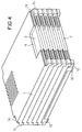
- Figur 1
- eine perspektivische Aufsicht schräg auf den erfindungsgemäßen Stecker,
Figur 2- eine Aufsicht auf die Rückseite eines Teilsteckers des Stapels gemäß Figur 1,
Figur 3- eine perspektivische Aufsicht von der Rückseite her auf den Stecker gemäß Figur 1,
Figur 4- eine andere Ausführung des Steckers gemäß der Erfindung in gleicher Darstellung wie Figur 1.
- Figure 1
- 2 shows a perspective top view obliquely of the plug according to the invention
- Figure 2
- 2 shows a top view of the rear of a partial connector of the stack according to FIG. 1,
- Figure 3
- 2 shows a perspective view from the rear of the plug according to FIG. 1,
- Figure 4
- another embodiment of the connector according to the invention in the same representation as Figure 1.
Der Stecker wird beispielsweise mittels der in Figur 1 erkennbaren
Flansche 16 auf einem nicht dargestellten Systemträger
befestigt. Dabei kann es sich insbesondere um eine
Leiterplatte handeln oder auch um die Gehäusewand eines elektronischen
Systems.The plug can be seen, for example, by means of the one shown in
Das Basiselement 12 und die zu stapelnden Rastelemente, also
die sonstigen Teilstecker 1, haben im Inneren bezüglich der
einzusteckenden Karte 3 und bezüglich der Kontaktfedern alle
den gleichen Aufbau, der aus Figur 2 hervorgeht. Der einzelne
Teilstecker 1, 12 hat an der Unterseite eine Kartenaufnahmekammer
2, in die die Karte 3 eingesetzt wird. Zum leichteren
Handling wir die Karte durch mindestens eine Andrücknase 11
in der Kartenaufnahmekammer 2 leicht festgeklemmt. An der
zweiten Stirnseite 13 ist eine Sichtöffnung 4 für die Karte
erkennbar. Zum Entfernen der Karte aus der Kartenaufnahmekammer
muß in der Ausführung gemäß den Figuren 1 bis 3, wie in
Figur 1 erkennbar, der frei zugreifbar offen liegende Kartenabschnitt
5 und 6 soweit angehoben werden, daß es zur
Entrastung, das heißt zur Trennung des Stapels an dem betreffenden
Platz kommt. Danach kann die Karte 3 aus der Kartenaufnahmekammer
2 entnommen werden. Bei der in Figur 4 dargestellten
Variante ist bei geringfügig größerer Breite des
Teilsteckers 1, 12 insgesamt das Stecken und Ziehen der Karten
3 möglich, ohne daß der Stapel getrennt werden muß. Dies
wird weiter unten noch näher erläutert. Die Baulänge der
Teilstecker 1, 12 kann bei dieser Variante im übrigen ohne
funktionelle Einbußen deutlich verringert werden, so daß die
Karten 3 an den zweiten Stirnseiten 13 deutlich überstehen
können. The
Das Verrasten der einzelnen Teilstecker 1, 12 im Stapel beruht,
wie beispielsweise aus den Figuren 1 und 3 hervorgeht,
im wesentlichen darauf, daß die Kontur der einzelnen Teilstecker
1, 12 so ausgebildet ist, daß ein mechanisch stabiles,
selbst arretierendes Ineinandergreifen einer Teilfläche
mit einer entsprechend als Negativ ausgebildeten Komplementärfläche
eines angrenzenden Teilsteckers beispielsweise
durch Auf- oder Einschnappen, durch Verschränken oder durch
Ineinanderdrücken möglich ist. In den dargestellten Ausführungsbeispielen
wird das federnde Verschnappen dadurch erreicht,
daß alle Teilstecker 1, 12 im oberen Bereich jeder
Stirnseite einen wenigstens über einen Teil der Breite der
jeweiligen Stirnseite verlaufenden Verriegelungsabschnitt 14
aufweisen und daß alle Teilstecker 1 mit Ausnahme des Basiselements
12 im unteren Bereich jeder Stirnseite mindestens einen
nach unten ragenden Rasthaken 15 aufweisen. Der Verriegelungsabschnitt
14 kann beispielsweise, wie dargestellt, als
Vertiefung ausgeführt sein. Die Rasthaken 15 können dann, wie
ebenfalls dargestellt, diese Vertiefungen klauenartig hintergreifen.
Diese Gestaltung erlaubt eine theoretisch unbegrenzte
Stapelgröße.The latching of the
Die Variante gemäß Figur 4 beruht im einzelnen darauf, daß
bei jedem Teilstecker 1, 12 die Rasthaken 15 an den Ecken der
zweiten Stirnseite 13 angeordnet sind und daß der untere Bereich
dieser Stirnseite 13 zwischen diesen beiden Rasthaken
15 auf einer Breite geöffnet ist, die groß genug ist, um das
Stecken oder Ziehen einer Karte in einem betreffenden Teilstecker
1, 12 ohne Trennen der Verrastung des betreffenden
Teilsteckers und des jeweils darunterliegenden Teilsteckers
zu erlauben.The variant according to FIG. 4 is based in detail on the fact that
for each
In Figur 3 ist erkennbar, daß die Steckeranschlüsse 7 aller
Teilstecker 1 mit Ausnahme des Basiselements 12 so ausgeführt
sind, daß sie die ihrem Reihenplatz entsprechenden Steckeranschlüsse
7 des im Stapel unmittelbar unter ihnen liegenden
Teilsteckers 1 kontaktieren. Im übrigen umfaßt der Grundgedanke
der vorliegenden Erfindung auch die Möglichkeit, daß
die Steckeranschlüsse der Kontaktfedern nicht stirnseitig aus
dem Teilstecker herausragen und demgemäß, wie bisher beschrieben,
im Außenbereich des Steckers miteinander verbunden
werden, sondern daß sie eine innen liegende Verbindung zwischen
Ober- und Unterseite jedes Teilsteckers herstellen, wie
dies analog in der Figur 4 und zugehöriger Beschreibung der
DE 195 23 793 C1 gezeigt ist.In Figure 3 it can be seen that the
Claims (6)
dadurch gekennzeichnet,
characterized by
dadurch gekennzeichnet,
characterized by
dadurch gekennzeichnet,
characterized by
dadurch gekennzeichnet,
characterized by
dadurch gekennzeichnet,
characterized by
dadurch gekennzeichnet,
characterized by
Applications Claiming Priority (2)
| Application Number | Priority Date | Filing Date | Title |
|---|---|---|---|
| DE19649599 | 1996-11-29 | ||
| DE19649599 | 1996-11-29 |
Publications (3)
| Publication Number | Publication Date |
|---|---|
| EP0845837A2 true EP0845837A2 (en) | 1998-06-03 |
| EP0845837A3 EP0845837A3 (en) | 1999-04-21 |
| EP0845837B1 EP0845837B1 (en) | 2001-01-31 |
Family
ID=7813187
Family Applications (1)
| Application Number | Title | Priority Date | Filing Date |
|---|---|---|---|
| EP97120219A Expired - Lifetime EP0845837B1 (en) | 1996-11-29 | 1997-11-18 | Connector comprising stacked modules for chip cards |
Country Status (3)
| Country | Link |
|---|---|
| EP (1) | EP0845837B1 (en) |
| AT (1) | ATE199050T1 (en) |
| DE (1) | DE59702971D1 (en) |
Cited By (15)
| Publication number | Priority date | Publication date | Assignee | Title |
|---|---|---|---|---|
| FR2783621A1 (en) * | 1998-09-22 | 2000-03-24 | Itt Mfg Enterprises Inc | Multimedia integrated circuit electrical connection unit having open ended slot box and base contacts underside integrated circuit connecting and having transverse box running slot outer contacts. |
| EP1079324A1 (en) * | 1999-08-25 | 2001-02-28 | Smartdata SA | Electronic apparatus comprising a group of smart cards |
| US6241557B1 (en) | 1999-03-26 | 2001-06-05 | Amphenol-Tuchel Electronics Gmbh | Smart card connector |
| DE10013134A1 (en) * | 2000-03-17 | 2001-09-20 | Moeller Gmbh | Assembly frame for circuit board e.g. for modular programmable control device, has locking device with catch for fastening frame to adjacent frame |
| EP1041676A3 (en) * | 1999-03-31 | 2002-02-13 | Yazaki Corporation | Press-contact joint connector |
| US6447338B1 (en) | 1999-05-07 | 2002-09-10 | Itt Manufacturing Enterprises, Inc. | One-piece smart card connector |
| NL1019122C2 (en) * | 2001-10-05 | 2003-04-08 | Framatome Connectors Int | Connector assembly comprises several connector wafers which have at least one side edge with several cavities and rib extending out of side wall of each cavity |
| US6913471B2 (en) | 2002-11-12 | 2005-07-05 | Gateway Inc. | Offset stackable pass-through signal connector |
| EP1615162A1 (en) * | 2004-07-07 | 2006-01-11 | Fujitsu Limited | Non-contact IC tag system |
| EP1688867A1 (en) | 2005-02-04 | 2006-08-09 | Chun-Hsin Ho | Dual universal integrated circuit card (UICC) system for a portable device |
| RU2391703C2 (en) * | 2005-12-06 | 2010-06-10 | Чун-Хсин Хо | System of dual card on integrated chips |
| RU2394272C2 (en) * | 2006-01-06 | 2010-07-10 | Чун-Хсин Хо | Method of rendering additional services based on double universal card on integrated circuits |
| US7866564B2 (en) | 2005-02-04 | 2011-01-11 | Chun-Hsin Ho | Dual card system |
| WO2011011096A1 (en) * | 2009-07-20 | 2011-01-27 | Sony Ericsson Mobile Communications Ab | Vertically stackable sockets for chip modules |
| EP2667454A1 (en) | 2012-05-25 | 2013-11-27 | Weetech GmbH | Variable plug connector |
Family Cites Families (4)
| Publication number | Priority date | Publication date | Assignee | Title |
|---|---|---|---|---|
| US4045105A (en) * | 1974-09-23 | 1977-08-30 | Advanced Memory Systems, Inc. | Interconnected leadless package receptacle |
| JP2555733Y2 (en) * | 1991-12-25 | 1997-11-26 | 住友電装株式会社 | connector |
| DE4435122C1 (en) * | 1994-09-30 | 1996-03-07 | Siemens Ag | Disk |
| DE19523793C1 (en) * | 1995-06-29 | 1996-11-07 | Siemens Ag | Stacking memory card connected to bus system |
-
1997
- 1997-11-18 EP EP97120219A patent/EP0845837B1/en not_active Expired - Lifetime
- 1997-11-18 DE DE59702971T patent/DE59702971D1/en not_active Expired - Fee Related
- 1997-11-18 AT AT97120219T patent/ATE199050T1/en not_active IP Right Cessation
Cited By (28)
| Publication number | Priority date | Publication date | Assignee | Title |
|---|---|---|---|---|
| EP1227428A1 (en) * | 1998-09-22 | 2002-07-31 | Itt Manufacturing Enterprises, Inc. | Electrical connector for an electronic memory card or smart card |
| WO2000017805A1 (en) * | 1998-09-22 | 2000-03-30 | Itt Manufacturing Enterprises, Inc. | Electrical connector for an electronic-memory card or smart card |
| US6544074B2 (en) | 1998-09-22 | 2003-04-08 | Itt Manufacturing Enterprises, Inc. | Electrical connector for smart card |
| FR2783621A1 (en) * | 1998-09-22 | 2000-03-24 | Itt Mfg Enterprises Inc | Multimedia integrated circuit electrical connection unit having open ended slot box and base contacts underside integrated circuit connecting and having transverse box running slot outer contacts. |
| US6241557B1 (en) | 1999-03-26 | 2001-06-05 | Amphenol-Tuchel Electronics Gmbh | Smart card connector |
| EP1041676A3 (en) * | 1999-03-31 | 2002-02-13 | Yazaki Corporation | Press-contact joint connector |
| US6461201B1 (en) | 1999-03-31 | 2002-10-08 | Yazaki Corporation | Press-contact joint connector |
| EP1764878A3 (en) * | 1999-03-31 | 2007-05-16 | Yazaki Corporation | Press-contact joint connector |
| US6447338B1 (en) | 1999-05-07 | 2002-09-10 | Itt Manufacturing Enterprises, Inc. | One-piece smart card connector |
| EP1079324A1 (en) * | 1999-08-25 | 2001-02-28 | Smartdata SA | Electronic apparatus comprising a group of smart cards |
| DE10013134A1 (en) * | 2000-03-17 | 2001-09-20 | Moeller Gmbh | Assembly frame for circuit board e.g. for modular programmable control device, has locking device with catch for fastening frame to adjacent frame |
| NL1019122C2 (en) * | 2001-10-05 | 2003-04-08 | Framatome Connectors Int | Connector assembly comprises several connector wafers which have at least one side edge with several cavities and rib extending out of side wall of each cavity |
| US6913471B2 (en) | 2002-11-12 | 2005-07-05 | Gateway Inc. | Offset stackable pass-through signal connector |
| US7145458B2 (en) | 2004-07-07 | 2006-12-05 | Fujitsu Limited | Non-contact IC tag system |
| EP1615162A1 (en) * | 2004-07-07 | 2006-01-11 | Fujitsu Limited | Non-contact IC tag system |
| EP1688867A1 (en) | 2005-02-04 | 2006-08-09 | Chun-Hsin Ho | Dual universal integrated circuit card (UICC) system for a portable device |
| CN100424720C (en) * | 2005-02-04 | 2008-10-08 | 何俊炘 | Dual universal integrated circuit card (uicc) system for a portable device |
| US7866564B2 (en) | 2005-02-04 | 2011-01-11 | Chun-Hsin Ho | Dual card system |
| RU2391703C2 (en) * | 2005-12-06 | 2010-06-10 | Чун-Хсин Хо | System of dual card on integrated chips |
| RU2394272C2 (en) * | 2006-01-06 | 2010-07-10 | Чун-Хсин Хо | Method of rendering additional services based on double universal card on integrated circuits |
| WO2011011096A1 (en) * | 2009-07-20 | 2011-01-27 | Sony Ericsson Mobile Communications Ab | Vertically stackable sockets for chip modules |
| US7922523B2 (en) | 2009-07-20 | 2011-04-12 | Sony Ericcson Mobile Communications Ab | Vertically stackable sockets for chip modules |
| CN102474036A (en) * | 2009-07-20 | 2012-05-23 | 索尼爱立信移动通讯有限公司 | Vertical stackable socket for chip modules |
| CN102474036B (en) * | 2009-07-20 | 2014-04-30 | 索尼爱立信移动通讯有限公司 | Vertical stackable socket for chip modules |
| EP2667454A1 (en) | 2012-05-25 | 2013-11-27 | Weetech GmbH | Variable plug connector |
| DE102012104549A1 (en) * | 2012-05-25 | 2013-11-28 | Weetech Gmbh | Variable connector of a connector |
| US9065193B2 (en) | 2012-05-25 | 2015-06-23 | Weetech Gmbh | Variable plug of a connector |
| DE102012104549B4 (en) * | 2012-05-25 | 2016-07-28 | Weetech Gmbh | Variable connector of a connector |
Also Published As
| Publication number | Publication date |
|---|---|
| ATE199050T1 (en) | 2001-02-15 |
| EP0845837B1 (en) | 2001-01-31 |
| DE59702971D1 (en) | 2001-03-08 |
| EP0845837A3 (en) | 1999-04-21 |
Similar Documents
| Publication | Publication Date | Title |
|---|---|---|
| DE69707730T2 (en) | Modular socket arrangement and universal housing for use therein | |
| EP0845837B1 (en) | Connector comprising stacked modules for chip cards | |
| DE3937383B4 (en) | Receiving device for chip cards | |
| DE3909263C3 (en) | Electrical connection device | |
| DE69500592T2 (en) | Grounded chip card | |
| DE10392323B4 (en) | Printed circuit board containing electrical connector assembly | |
| EP0845750A2 (en) | Double connector for two chip cards | |
| DE69529796T2 (en) | Double row flat plug connector with low height | |
| EP0900460A1 (en) | Catch system for a pin-and-socket connector coupling | |
| DE4221017A1 (en) | CONNECTOR FOR ELECTRICALLY CONNECTING SEMICONDUCTOR DEVICES TO A SUBSTRATE | |
| DE10204006B4 (en) | Multiple Connectors | |
| DE60108333T2 (en) | Electrical connector | |
| DE4444923A1 (en) | Printed circuit board with I / O connection areas on secondary areas | |
| DE102004031993B4 (en) | Connector and connector provided with such a connector | |
| DE7917511U1 (en) | Box element for receiving electrical contact socket elements | |
| DE102018128042A1 (en) | Set of connector and retaining element and connector and retaining element for this purpose | |
| DE102020123188A1 (en) | Modular connector for contacting a mating connector, in particular a printed circuit board connector | |
| DE19717984A1 (en) | Electric connector with knife contact and socket contact | |
| DE3216217A1 (en) | MODULE PLUG | |
| DE69503509T2 (en) | SIM CARD CONNECTOR | |
| EP0177731A2 (en) | Plug-in electrical module | |
| EP0474082A1 (en) | Coding device with integrated special contacts for electrical assemblies pluggable on a back panel wiring | |
| DE2363597A1 (en) | ELECTRIC PLUG | |
| EP0845838A2 (en) | Electrical plug connector | |
| DE2938014A1 (en) | ELECTRICAL CONNECTOR |
Legal Events
| Date | Code | Title | Description |
|---|---|---|---|
| PUAI | Public reference made under article 153(3) epc to a published international application that has entered the european phase |
Free format text: ORIGINAL CODE: 0009012 |
|
| AK | Designated contracting states |
Kind code of ref document: A2 Designated state(s): AT BE CH DE FI FR GB IT LI NL SE |
|
| AX | Request for extension of the european patent |
Free format text: AL;LT;LV;MK;RO;SI |
|
| PUAL | Search report despatched |
Free format text: ORIGINAL CODE: 0009013 |
|
| AK | Designated contracting states |
Kind code of ref document: A3 Designated state(s): AT BE CH DE DK ES FI FR GB GR IE IT LI LU MC NL PT SE |
|
| AX | Request for extension of the european patent |
Free format text: AL;LT;LV;MK;RO;SI |
|
| 17P | Request for examination filed |
Effective date: 19990520 |
|
| AKX | Designation fees paid |
Free format text: AT BE CH DE FI FR GB IT LI NL SE |
|
| GRAG | Despatch of communication of intention to grant |
Free format text: ORIGINAL CODE: EPIDOS AGRA |
|
| 17Q | First examination report despatched |
Effective date: 20000207 |
|
| RAP1 | Party data changed (applicant data changed or rights of an application transferred) |
Owner name: TYCO ELECTRONICS LOGISTICS AG |
|
| GRAG | Despatch of communication of intention to grant |
Free format text: ORIGINAL CODE: EPIDOS AGRA |
|
| GRAH | Despatch of communication of intention to grant a patent |
Free format text: ORIGINAL CODE: EPIDOS IGRA |
|
| GRAH | Despatch of communication of intention to grant a patent |
Free format text: ORIGINAL CODE: EPIDOS IGRA |
|
| GRAA | (expected) grant |
Free format text: ORIGINAL CODE: 0009210 |
|
| AK | Designated contracting states |
Kind code of ref document: B1 Designated state(s): AT BE CH DE FI FR GB IT LI NL SE |
|
| PG25 | Lapsed in a contracting state [announced via postgrant information from national office to epo] |
Ref country code: SE Free format text: LAPSE BECAUSE OF FAILURE TO SUBMIT A TRANSLATION OF THE DESCRIPTION OR TO PAY THE FEE WITHIN THE PRESCRIBED TIME-LIMIT Effective date: 20010131 Ref country code: NL Free format text: LAPSE BECAUSE OF FAILURE TO SUBMIT A TRANSLATION OF THE DESCRIPTION OR TO PAY THE FEE WITHIN THE PRESCRIBED TIME-LIMIT Effective date: 20010131 Ref country code: IT Free format text: LAPSE BECAUSE OF FAILURE TO SUBMIT A TRANSLATION OF THE DESCRIPTION OR TO PAY THE FEE WITHIN THE PRE;WARNING: LAPSES OF ITALIAN PATENTS WITH EFFECTIVE DATE BEFORE 2007 MAY HAVE OCCURRED AT ANY TIME BEFORE 2007. THE CORRECT EFFECTIVE DATE MAY BE DIFFERENT FROM THE ONE RECORDED.SCRIBED TIME-LIMIT Effective date: 20010131 Ref country code: FI Free format text: LAPSE BECAUSE OF FAILURE TO SUBMIT A TRANSLATION OF THE DESCRIPTION OR TO PAY THE FEE WITHIN THE PRESCRIBED TIME-LIMIT Effective date: 20010131 |
|
| REF | Corresponds to: |
Ref document number: 199050 Country of ref document: AT Date of ref document: 20010215 Kind code of ref document: T |
|
| REG | Reference to a national code |
Ref country code: CH Ref legal event code: EP |
|
| GBT | Gb: translation of ep patent filed (gb section 77(6)(a)/1977) |
Effective date: 20010209 |
|
| REF | Corresponds to: |
Ref document number: 59702971 Country of ref document: DE Date of ref document: 20010308 |
|
| ET | Fr: translation filed | ||
| NLV1 | Nl: lapsed or annulled due to failure to fulfill the requirements of art. 29p and 29m of the patents act | ||
| PG25 | Lapsed in a contracting state [announced via postgrant information from national office to epo] |
Ref country code: AT Free format text: LAPSE BECAUSE OF NON-PAYMENT OF DUE FEES Effective date: 20011118 |
|
| PG25 | Lapsed in a contracting state [announced via postgrant information from national office to epo] |
Ref country code: LI Free format text: LAPSE BECAUSE OF NON-PAYMENT OF DUE FEES Effective date: 20011130 Ref country code: CH Free format text: LAPSE BECAUSE OF NON-PAYMENT OF DUE FEES Effective date: 20011130 Ref country code: BE Free format text: LAPSE BECAUSE OF NON-PAYMENT OF DUE FEES Effective date: 20011130 |
|
| PLBE | No opposition filed within time limit |
Free format text: ORIGINAL CODE: 0009261 |
|
| STAA | Information on the status of an ep patent application or granted ep patent |
Free format text: STATUS: NO OPPOSITION FILED WITHIN TIME LIMIT |
|
| REG | Reference to a national code |
Ref country code: GB Ref legal event code: IF02 |
|
| 26N | No opposition filed | ||
| BERE | Be: lapsed |
Owner name: TYCO ELECTRONICS LOGISTICS A.G. Effective date: 20011130 |
|
| REG | Reference to a national code |
Ref country code: CH Ref legal event code: PL |
|
| PGFP | Annual fee paid to national office [announced via postgrant information from national office to epo] |
Ref country code: GB Payment date: 20041004 Year of fee payment: 8 |
|
| PGFP | Annual fee paid to national office [announced via postgrant information from national office to epo] |
Ref country code: FR Payment date: 20041105 Year of fee payment: 8 |
|
| PG25 | Lapsed in a contracting state [announced via postgrant information from national office to epo] |
Ref country code: GB Free format text: LAPSE BECAUSE OF NON-PAYMENT OF DUE FEES Effective date: 20051118 |
|
| GBPC | Gb: european patent ceased through non-payment of renewal fee |
Effective date: 20051118 |
|
| PG25 | Lapsed in a contracting state [announced via postgrant information from national office to epo] |
Ref country code: FR Free format text: LAPSE BECAUSE OF NON-PAYMENT OF DUE FEES Effective date: 20060731 |
|
| REG | Reference to a national code |
Ref country code: FR Ref legal event code: ST Effective date: 20060731 |
|
| PGFP | Annual fee paid to national office [announced via postgrant information from national office to epo] |
Ref country code: DE Payment date: 20070102 Year of fee payment: 10 |
|
| PG25 | Lapsed in a contracting state [announced via postgrant information from national office to epo] |
Ref country code: DE Free format text: LAPSE BECAUSE OF NON-PAYMENT OF DUE FEES Effective date: 20080603 |