BACKGROUND OF THE INVENTION
The present invention relates to the lens system in a projection exposure
apparatus used for manufacturing semiconductor devices or liquid crystal
devices and the like via photolithographic processing. The invention
specifically relates to a catadioptric lens system which is capable of providing
a photolithographic resolution of quarter micron levels in the ultraviolet band
region by using a reflective mirror as an element of the lens system.
In photolithographic processing for manufacturing semiconductor
devices and the like, a projection exposure apparatus is used in which a
semiconductor device pattern printed onto a photomask or reticle (hereafter
both are referred to as reticle) is exposed via a projection lens system onto a
substrate such as a wafer or glass plate (hereafter both are referred to as a
wafer) coated with photoresist and the like. As integration of semiconductor
devices and the like advances, demand for a projection lens system used in
projection exposure apparatus requiring more stringent resolution increases.
In order to fulfill this need, using a shorter band illumination light and using a
larger numerical aperture (NA) for a projection lens system have become
essential. Various technologies have been proposed in order to meet the
requirement in which a projection lens system is constructed with a so called
"catadioptric lens system" which is a combination of a reflective system and a
refractive system.
For example, Japanese patent kokai S63-163319 and kokai H5-25170
disclose a catadioptric lens system which uses an exposure region including
light on the optical axis.
In addition, kokai H7-111512 and US 4,779,966 use light on the
exposure region of a ring field, rather than light on the optical axis.
In the catadioptric lens system using an exposure region which includes
light on the optical axis, a beam splitter having a transmittive reflective surface
is required for splitting the optical path. This lens system may easily generate
light aberrations, causing flares or uneven illumination on the surface of a
wafer. These light aberrations are generated from internal reflections from the
wafer surface, from a refractive surface of the lens systems arranged behind
the beam splitter, or from the transmittive reflective surface of a beam splitter
and the like. A lens system with a larger numerical aperture requires a larger
beam splitter and a longer exposure time due to the decrease in light intensity.
This in turn, causes a decrease in throughput of the semiconductor
manufacturing process. Also, as disclosed in Japanese patent kokai H6-300973,
a reflection beam splitter is required to prevent loss of light intensity,
however, it is very difficult to manufacture a large reflection beam splitter and
its use gives unfavorable imaging performance due to the uneven film
thickness of the transmittive reflective layer, which affects the deflection,
absorption, and phase change of the light, etc.
On the other hand, in the catadioptric lens system disclosed in US
4,779,966 using a ring exposure field, a reflective lens system is employed on
the reduced side toward a wafer surface rather than at an interim image.
However, the NA is larger on the reduced side than on the reticle surface side.
It is difficult to split the optical path, making it impossible to increase the NA of
the lens system. This does not provide excellent resolution. The size of the
concave mirror cannot be increased either.
In the catadioptric lens system disclosed in Japanese patent kokai H7-111512
using a ring exposure field, the first lens systemincluding a concave
mirror for forming an interim image is constructed with a lens system in perfect
symmetry, and the size of the interim image remains the same as the real size
of the reticle surface. In this way, the possibility of generating aberrations in
the first imaging lens is reduced, however, this gives a heavier load onto the
second imaging lens system. Especially, when a large NA is required for the
lens system, it is inevitable that the size and complexity of the second lens
systemmust be increased.
The present invention intends to resolve the problem by providing a
catadioptric lens system whose entire size is essentially compact and is
capable of providing a large numerical aperture in the ultraviolet band region
to obtain the photolithographic resolution of quarter micron levels and is
constructed with components of reduced sizes.
SUMMARY OF THE INVENTION
In order to accomplish the above object, the present invention provides
a catadioptric lens system characterized by the fact that the catadioptric lens
system comprises:
The invention further relates to a catadioptric lens system comprising:
Moreover, the catadioptric lens system of the present invention is
further characterized by a) a first lens system constructed with refractive
members,
b) a concave mirror, and c) a second lens system constructed with refractive
members to project a semiconductor device pattern from a reticle surface onto
a substrate wherein the first lens system comprises:
BRIEF DESCRIPTION OF THE DRAWINGS
Figure 1 shows a layout of a catadioptric lens system of embodiment 1.
Figure 2 shows an aberration diagram of a catadioptric lens system of
embodiment 1.
Figure 3 shows a layout of a catadioptric lens system of embodiment 2.
Figure 4 shows an aberration diagram of a catadioptric lens system of
embodiment 2.
BRIEF DESCRIPTION OF THE PREFERRED EMBODIMENTS
In the present embodiment, as described, the chance of generating
aberrations of high orders is reduced and the NA of the lens system is
increased, thus preventing an increase in the complexity and size of the lens
system. Changing the refractive surface from a spherical surface ideally
bends light flux which exists around the lens surface. This makes it possible to
correct aberrations of high orders without broadening the entire flux.
Introducing aspherical refractive surfaces to the first lens system S1,
prevents increasing the size of it. Introducing aspherical refractive surfaces to
the second lens system S2, also prevents increasing the size of it.
Also, it is preferable that the first lens system S1 comprises a first lens
group G1, in which light enters only once and a second lens group G2 in which
light makes a round trip. The lens closest to the concave mirror M1 of the
second lens group G2 is a negative lens LS. Light coming through the second
lens group G2 images a semiconductor device pattern once before entering
the second lens system S2. This configuration of the lens system especially
allows decreasing the size of each of its component members. In addition, the
configuration is very effective in reducing chromatic aberration on the axis
wherein the configuration includes, in order in which light progresses, a
negative lens LS which is closest to the concave mirror M1 in the second lens
group G2, a concave mirror M1, and the second lens system S2 wherein the
semiconductor device pattern is imaged once before light emitted from the
second lens group G2 enters the second lens system S2.
In the lens system of the aforementioned configuration, it is preferable
that the second lens group G2 is constructed with a refractive member having
at least two different negative refractive powers and a refractive member
having at least two different positive refractive powers. The lens having
negative refractive powers is effective in correcting coma or spherical
aberrations and image curvature and the like. The lens having positive
refractive powers is effective in not increasing the size of the lens system and
provides a large NA or exposure region. Moreover, it is desirable that each of
the members have at least two lenses in order to reduce the load for correcting
aberrations of the second lens systemS2.
Also, it is preferable that the first lens group G1 is constructed with
refractive members having three different refractive powers. Lately, as the
demand for higher resolution increases, more stringent specifications are
demanded for correcting distortion, image curvature and the like. It is
important for one to adjust these parameters during manufacturing to meet this
demand. These adjustments for a lens positioned in the vicinity of the reticle
surface work effectively. The second lens group G2 of the present invention,
is the lens system for both outgoing and incoming light, which is inappropriate
for adjustment lenses. For this reason, constructing the first lens group G1
with lenses having at least three different refractive powers makes it possible
to adjust distortion or curvature aberration during manufacturing of lens
systems. Also, by utilizing the first lens group G1 in the aforementioned
configuration, the working distance in the vicinity of the surface of the reticle R
can be increased and a step and scan method of exposure is made possible.
The second lens system S2 plays an important role in correcting mainly
spherical or coma aberrations to allow the lens system to have a large NA.
In the present invention, it is preferable to arrange a second optical path
reflection member M3 between the first lens system S1 and the second lens
system S2 or in the second lens system S2. Also, it is possible to dispose the
reflection member M3 in the second imaging lens system. By installing an
optical path reflection member such as a mirror, the entire lens system can be
bent, reducing its entire size.
Short band wavelengths, in excess of 300nm, are used as the light
source in the present invention, therefore, quartz or fluorite are preferable as
the material for a refraction member. These minerals are excellent in
illumination transmissivity, they are inexpensive, and they are easy to process.
Also in the present invention, the concave mirror M1 can be formed
aspherically. If a concave minor M1 is aspherical, the magnitude of the
positive refractive power of the concave mirror M1 can be increased without
generating aberrations of high orders which makes it possible to manufacture
compact lens systems having a large NA and also allows correcting chromatic
aberration over a wide bandwidth.
Note that by forming an aperture stop (variable aperture) in the optical
path of the second lens system S2, the coherence factor (σ value) can be
adjusted. A technique to increase focal depth and improve resolution is
disclosed for example in Japanese patent kokai S62-50811 in which a phase
shift technique is used to shift the phase of a predetermined portion of the
reticle pattern from another portion. The present invention provides increased
effect of the phase shift technique with adjustment of the coherence factor (σ
value).
The examples expressed quantitatively for the catadioptric lens system
of the present invention are shown herein. The catadioptric lens system in
each of the quantitative embodiments comprises, in order from the reticle R
side (in the order that light progresses):
NA=0.6 in each of the quantitative embodiments, and aberrations for the
image height are corrected within the range of about 5 to about 18.6. Note
that the range for the aforementioned image height may be a ring field or may
be a rectangle of 6 x 30 at a distance of 5 from the optical axis.
In each of the tables in embodiments 1 and 2, r denotes surface
curvature radius and d denotes a distance between surfaces. Glassy
materials are denoted as SiO
2 for quartz and CaF
2 for fluorite in each of the
tables. The refraction rates for quartz and fluorite for n, at 193.0 nm, and for
1/v, which is the dispersion value for those of ± 0.1nm, are as follows:
| | n | 1 /v |
| synthetic quartz: | 1.56019 | 1780 |
| fluorite | 1.50138 | 2550 |
In each of the embodiments, an aspherical surface is shown by the
following equation where:
- Z:
- distance from the top measured in the direction of the optical axis.
- Y:
- distance from the top measured in the direction perpendicular to
the optical axis.
- K:
- constant of the cone.
- r:
- curvature radius of the top.
- C4, C6, C8.....:
- constants for 4-order, 6-order, 8-order aspherical surface.
Z = (Y2 / r) / [1 + sqrt {1- (1 + K) Y2 / r}] + C4 Y4 + C6 Y6 + C8 Y8 + C10 Y10 + C12
Y12
In the first embodiment 1, a first lens group G1 comprises, in order from
the side of the surface of the reticle R, a biconvex lens 10, a biconcave lens
11, a meniscus lens 12 whose convexity points to the side of the surface of the
reticle R, and parallel plane plates 13. The second lens group comprises, in
order from the surface of the reticle R, a biconvex lens 14, a biconcave lens
15, a biconvex lens 16, a biconcave lens 17, a biconvex lens 18, a meniscus
lens 19 whose concavity points to the side of the surface of the reticle R, a
biconvex lens 20, a meniscus lens 21 whose convexity points to the side of the
surface of the reticle R, and a negative meniscus lens LS whose concavity
points to the surface of the reticle R and is formed with an aspherical surface
AS1 on the side of the reticle R. Parallel plane plates 13 in the first lens group
G1 comprise a plane mirror M2 which is made by polishing a part of the lens to
function as a first optical path reflection member M2. The image of the reticle
R is formed once in the vicinity of the plane mirror M2. Also in the present
embodiment, the concave minor M1 is formed on an aspherical surface AS2.
In addition, the second lens system S2 comprises, in order from the
surface of the reticle R, a biconvex lens 22 (which can be arranged in the
second lens system S2 or can be arranged between the first and second lens
systems S1and S2 respectively), a meniscus lens 23 whose concavity points
to the side of the surface of the reticle R, a biconvex lens 24, a meniscus lens
25 whose convexity points to the side of the surface of the reticle R, a
biconvex lens 26, an aperture stop AP, a bioconvex lens 27, a meniscus lens
28 formed with an aspherical surface AS3 whose convexity points to the
surface of the reticle R, a meniscus lens 29 whose convexity points to the side
of the surface of the reticle R, a meniscus lens 30 whose convexity points to
the side of the surface of the reticle R, a biconcave lens 31, a meniscus lens
32 whose concavity points to the side of the surface of the reticle R, and a
meniscus lens 33 whose convexity points to the side of the surface of the
reticle R. Now, in the present embodiment, a plane mirror M3 is arranged
optically between the first lens 22 and the second lens 23 of the second lens
system S2 or in the second lens system S2 such that surfaces of a reticle R
and a wafer W are arranged in parallel.
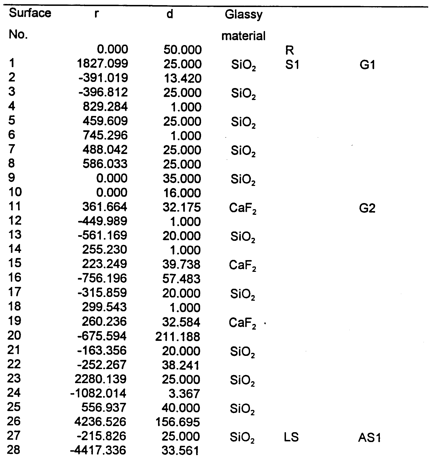


As described above, the required parameters comprise a NA of 0.6, the
image height Y of 18.6, and the diameter of about 20 for all optical members of
the catadioptric lens system. Figure 2 shows a horizontal aberration diagram
for the catadioptric lens system of the present embodiment. Aberrations are
measured for each bandwidth using the image height Y = 18.6 for (a) and Y =
5 for (b) with the unit Y in millimeters (mm). As is clear from Figure 2,
aberrations are corrected very well by the reflective-refractive optical system
of the present embodiment.
In the second embodiment 2, a first lens group G1 of the first lens
system comprises, in order from the surface of the reticle R, a meniscus lens
34 whose convexity points to the side of the surface of the reticle R, a
biconvex lens 35, a biconcave lens 36, a meniscus lens 37 whose convexity
points to the side of the surface of the reticle R, and parallel plane plate 38.
The second lens group G2 of the first lens system comprises, in order from the
surface of the reticle R, a biconvex lens 39, a meniscus lens 40 whose
concavity points to the side of the surface of the reticle, a biconvex lens 41, a
meniscus lens 42 whose convexity points to the side of the surface of the
reticle R, biconcave lens 43, biconvex lens 44, a meniscus lens 45 whose
convexity points to the side of the surface of the reticle R, a biconvex lens 46,
a meniscus lens 47 whose concavity points to the side of the surface of the
reticle R, and a negative meniscus lens LS whose concavity points to the
surface of the reticle R. Parallel plane plates in the first lens group G1
comprises a plane mirror M2 which is made by polishing a surface of the lens
to function as an optical reflection member. The image of the reticle R is
formed once in the vicinity of the plane mirror M2. Also in the present
embodiment, the concave mirror M1 is formed on an aspherical surface AS2.
In addition, the second lens system S2 comprises, in order from the
surface of the reticle R, a biconvex lens 48, a meniscus lens 49 whose
convexity points to the side of the surface of the reticle R, (the biconvex lens
48 and the meniscus lens 49 may be arranged within the second lens system
S2 or between the first and second lens systems S1 and S2 respectively),
meniscus lens 50 whose convexity points to the side of the surface of the
reticle R, a meniscus lens 51 whose concavity points to the side of the surface
of the reticle R, an aperture stop P, a biconvex lens 52 whose surface on the
side of the reticle R is formed with an aspherical surface AS2, a meniscus lens
53 whose convexity points to the side of the surface of the reticle R, a
biconcave lens 54, a meniscus lens 55 whose convexity points to the side of
the surface of the reticle R, a meniscus lens 56 whose convexity points to the
side of the surface of the reticle R, and a biconvex lens 57. Now, in the
present embodiment, a plane mirror M3 is arranged between the lens 49 and
the lens 50 in the second lens system S2 such that surfaces of a reticle R and
a wafer W are arranged in parallel.

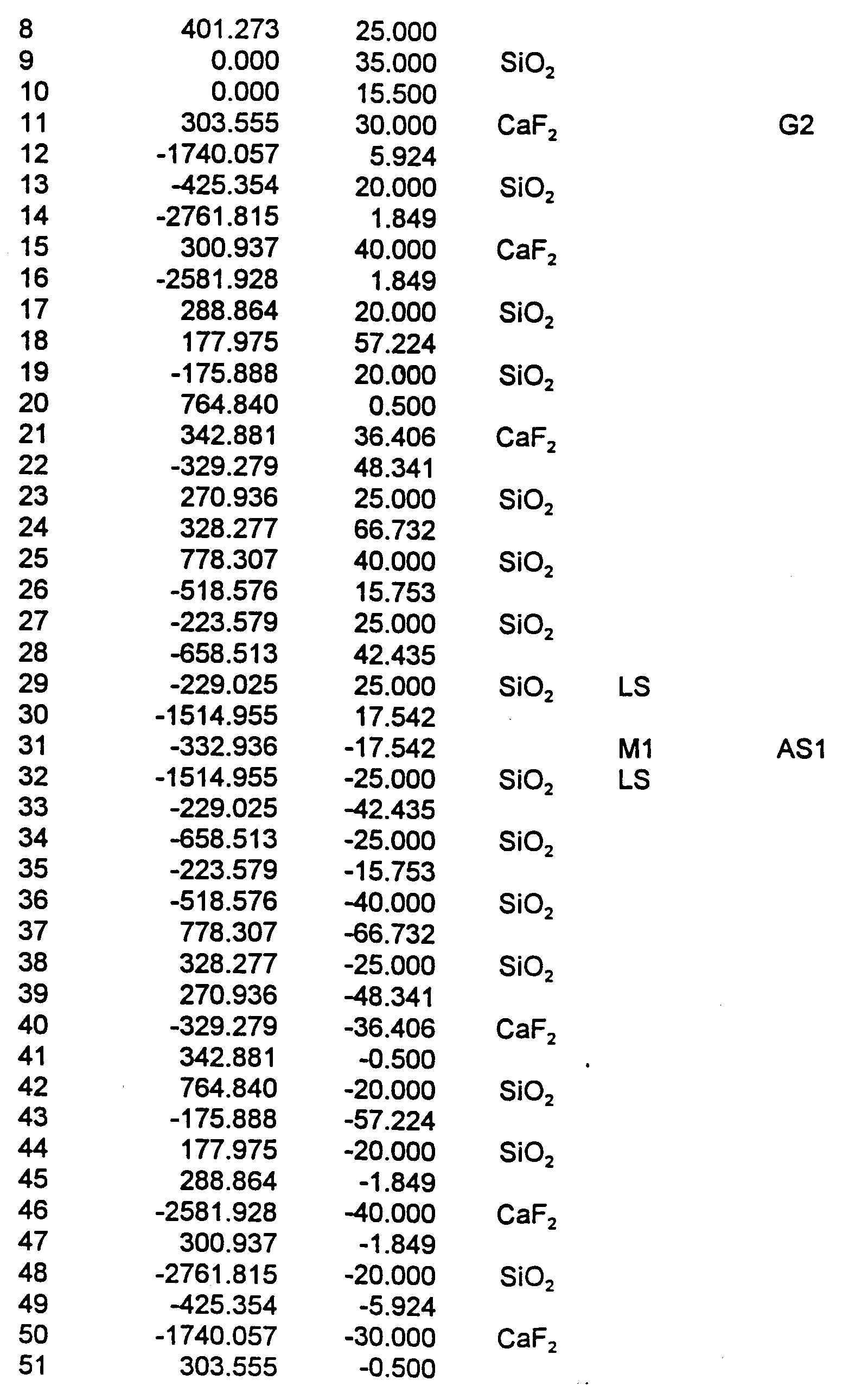

As described above, the required parameters comprise a NA of 0.6, an
image height Y of 18.6, and a diameter of about 20 for all optical members of
the catadioptric lens system. Figure 4 shows a horizontal aberration diagram
for the catadioptric lens system of the present embodiment. Aberrations are
measured for each bandwidth using the image height Y = 18.6 for (a) and Y =
5 for (b). As is clear from Figure 4, aberrations are corrected very well by the
reflective-refractive optical system of the present embodiment.
As described, the present invention can provide a catadioptric lens
system whose entire size is practically compact and is capable of providing a
large numerical aperture in the ultraviolet band. The invention also provides
photolithographic resolution of quarter micron levels and is easy to
manufacture.


