EP0738008A2 - Semiconductor power module - Google Patents
Semiconductor power module Download PDFInfo
- Publication number
- EP0738008A2 EP0738008A2 EP96810191A EP96810191A EP0738008A2 EP 0738008 A2 EP0738008 A2 EP 0738008A2 EP 96810191 A EP96810191 A EP 96810191A EP 96810191 A EP96810191 A EP 96810191A EP 0738008 A2 EP0738008 A2 EP 0738008A2
- Authority
- EP
- European Patent Office
- Prior art keywords
- module
- control unit
- base plate
- connections
- power
- Prior art date
- Legal status (The legal status is an assumption and is not a legal conclusion. Google has not performed a legal analysis and makes no representation as to the accuracy of the status listed.)
- Granted
Links
Images


Classifications
-
- H10W90/00—
-
- H10W70/682—
-
- H10W70/685—
-
- H10W72/07554—
-
- H10W72/5363—
-
- H10W72/547—
-
- H10W72/5475—
-
- H10W90/754—
Definitions
- the invention relates to the field of power electronics.
- the power connections run perpendicular to the base plate (see DE 39 31 634 Fig. 4 and column 5, lines 24 ff. And DE 43 30 070 Fig. 8).
- the Power connections are led out of the module housing perpendicular to the base plate.
- the control units must be arranged at a certain distance, for example above or next to the modules. This entails relatively long connection lines to the control unit, which is used to control the module.
- the long connecting lines result in an undesirably high inductance of the arrangement, which can have a limiting effect particularly with regard to high switching frequencies.
- the object of the present invention is therefore to provide a power semiconductor module in which the connecting lines to the control unit are as short as possible and the arrangement is thereby as low-inductance as possible.
- the essence of the invention is therefore that the power connections run parallel to the base plate and are led out of the housing parallel to the base plate. This makes it possible to mount the control unit directly on the surface of the module housing facing away from the base plate. This enables the use of short connecting lines and thus a low-inductance structure.
- control connection which has the smallest, ideally none, potential difference compared to the control unit is located furthest away from the base plate, this power connection just acts for the control unit as a shield for electromagnetic fields, which are caused by switching the module.
- fastening means such as screw holes and screws are provided on the side of the module housing facing away from the base plate.
- the control and auxiliary connections can be led out on the top of the housing.
- the control unit is then plugged into these connections and the connection between the control and auxiliary connections of the module and the corresponding connections of the control unit is made e.g. by means of simple screw or plug contacts.
- modules according to the invention it is thus possible to produce circuit arrangements in which the control unit of the modules is mounted directly on the modules and in which the connection between module and control unit can advantageously be established in a low-inductance manner, so that the modules can be used in particular for higher frequencies.
- FIG. 3 shows the structure of a circuit arrangement with a power semiconductor module 1 and a control unit 12.
- the control unit 12 is fastened on the housing 2 of the module 1, for example by means of screws 10 which are guided through corresponding screw holes 11.
- the module housing 2 can also have screw holes 8, which are used for fastening in a system.
- the power semiconductor module 1 has a number of control and auxiliary connections 13, which are connected to the control unit 12, in particular by means of a plug connection.
- the control and auxiliary connections serve on the one hand to switch module 1 on and off and on the other hand to monitor it.
- Module 1 also has at least two Power connections 5 and 6, which are led laterally out of the housing 2.
- a load connection 7 is also provided. Since the control unit 12 is packed directly onto the housing 2 of the module, the connecting lines between the control and auxiliary connections 13 and the control unit can be selected to be very short and thus of low inductance.
- the power connections 5 and 6 run parallel to a base plate 3, to which a power semiconductor switching element 4 is applied.
- the power semiconductor switching element is in particular an IGBT chip, i.e. a bipolar transistor chip with an isolated gate.
- FIG. 2 shows from above and FIG. 1 in section, the connection between the power electrodes and the corresponding power connections 5 and 6 can be established, for example, by means of bonding wires 9.
- a power semiconductor module 1 is therefore basically constructed as follows: Ceramic substrates 15 are soldered to a base plate 3, for example an 8 mm thick copper plate, which can possibly also serve as a cooler.
- the substrates are each assigned to a switching element 4. This includes, for example, at least one IGBT chip with an associated free-wheeling diode.
- the substrates 15 are metallized over the entire surface.
- the power connections 5, 6 and possibly 7 are supplied from the side by means of connecting lines 9, in particular by means of bond wires ("wirebonds") or soldered strips (“solder clips").
- the connecting lines 9 lead to the corresponding power connections 5 and 6, possibly to the load connection 7 and to the control and auxiliary connections 13, which are arranged in different levels and run parallel to the base plate.
- the power connections 5, 6 and possibly 7 are led out of the housing 2 laterally parallel to the base plate 3.
- the auxiliary and control connections 13 can be brought out at right angles to the base plate 3.
- the control unit 12 can be connected to these connections by simply plugging them onto the corresponding connections.
- this power connection also serves as an electromagnetic shield. This protects the control unit 12 from the influence of the electromagnetic fields caused by the switching of the module. These fields are caused by the high currents and voltages that should be switched with the module in the shortest possible time. Without special shielding, the fields can lead to serious malfunctions of a power electronic circuit arrangement and, in addition to other influencing factors, also hinder the further development of higher switching frequencies.
- FIG. 4 shows the equivalent circuit diagram of a half-bridge.
- the switching elements are each at least one switch chip, here in the form of an IGBT (IGBT1, IGBT2), with an associated freewheeling diode D1, D2.
- IGBT IGBT
- the common node corresponds to the load connection 7
- the plus and minus connection corresponds to the load connections 5 and 6.
- the two IGBTs are each controlled by a gate or control connection 13.
- Figure 5 shows such a module in section: on the base plate 3 are the substrates 15 of the switching elements 4, i.e. of the IGBTs (IGBT1, IGBT2, 4) attached.
- the power connections 5 and 6 and the common load connection 7 are arranged in different levels and are connected to the corresponding electrodes of the semiconductor switches via the connection wires 9.
- the two control connections 13 of the IGBTs are arranged on the same connection level.
- the corresponding connection level e.g. by means of conductor tracks, structured so that the connections are electrically separated.
- Insulating layers 14 must be inserted between two adjacent levels or connections. It is of course also conceivable to arrange 3 substrates and switching elements on both sides of the base plate.
Landscapes
- Power Conversion In General (AREA)
- Inverter Devices (AREA)
Abstract
Es wird ein Leistungshalbleitermodul angegeben, bei welchem die Leistungsanschlüsse parallel zu einer Grundplatte verlaufen. Dadurch kann die Steuereinheit direkt auf dem Gehäuse angeordnet werden und es resultiert aufgrund der kurzen Verbindungsleitungen ein niederinduktiver Aufbau.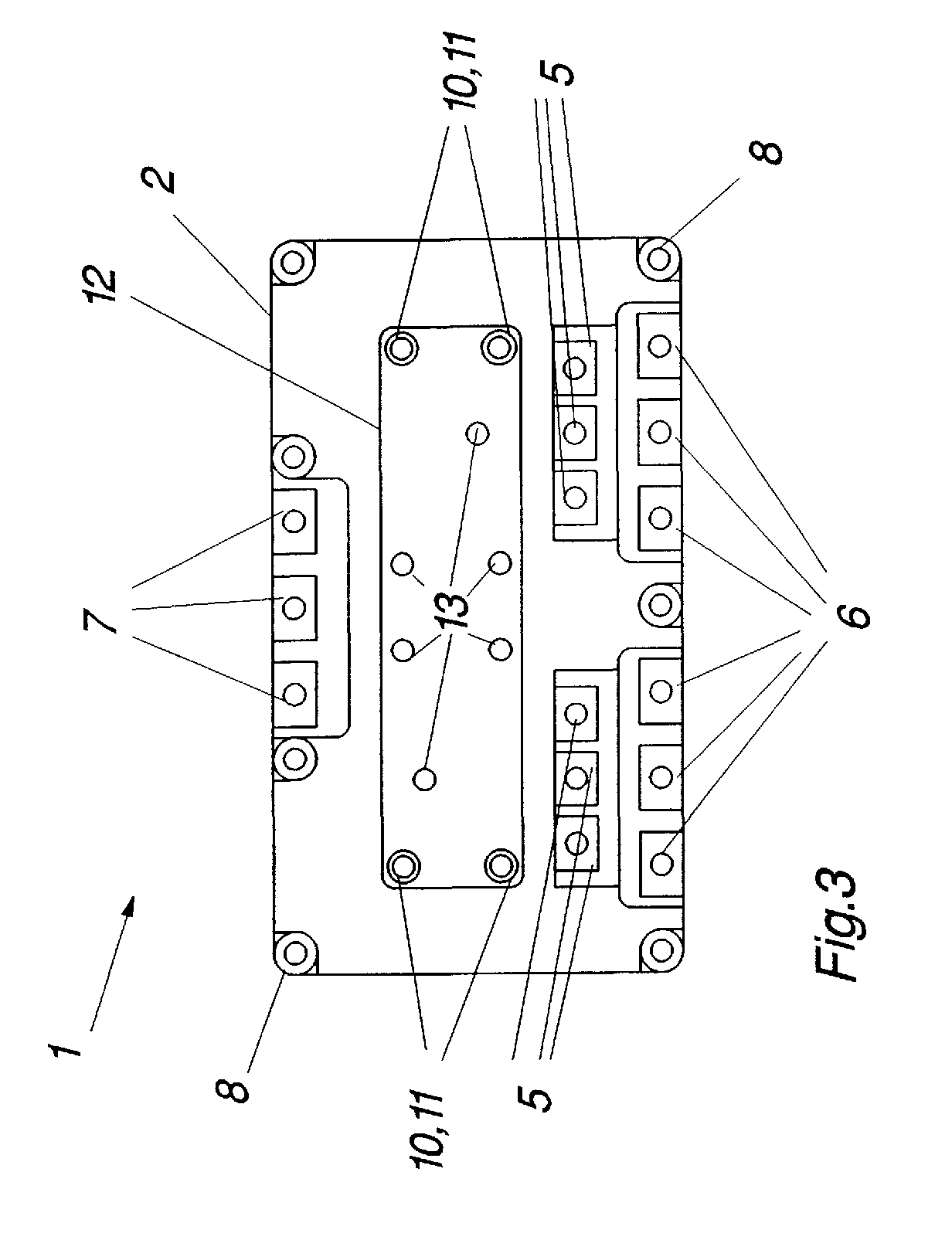
Description
Die Erfindung bezieht sich auf das Gebiet der Leistungselektronik.The invention relates to the field of power electronics.
Sie geht aus von einem Leistungshalbleitermodul nach dem Oberbegriff des ersten Anspruchs.It is based on a power semiconductor module according to the preamble of the first claim.
Solche Leistungshalbleitermodule werden beispielsweise schon in den deutschen Offenlegungsschriften DE-A1-39 31 634 und DE-A1-43 30 070 beschrieben.Power semiconductor modules of this type are already described, for example, in German Offenlegungsschriften DE-A1-39 31 634 and DE-A1-43 30 070.
Bei diesen Leistungshalbleitermodulen, welche eine Grundplatte mit mindestens einem Leistungshalbleiterschaltelement umfassen, verlaufen die Leistungsanschlüsse senkrecht zur Grundplatte (siehe DE 39 31 634 Fig. 4 und Spalte 5, Zeilen 24 ff. und DE 43 30 070 Fig. 8). Die Leistungsanschlüsse werden senkrecht zur Grundplatte aus dem Modulgehäuse geführt. Dadurch müssen die Steuereinheiten in einer gewissen Entfernung z.B. oberhalb oder neben den Modulen angeordnet werden. Dies zieht relativ lange Anschlussleitungen zur Steuereinheit, welche der Ansteuerung des Moduls dient, mit sich. Die langen Anschlussleitungen ergeben eine unerwünscht hohe Induktivität der Anordnung, welche insbesondere im Hinblick auf hohe Schaltfrequenzen limitierend wirken kann.In these power semiconductor modules, which comprise a base plate with at least one power semiconductor switching element, the power connections run perpendicular to the base plate (see DE 39 31 634 Fig. 4 and
Aufgabe der vorliegenden Erfindung ist es deshalb, ein Leistungshalbleitermodul anzugeben, bei welchem die Verbindungsleitungen zur Steuereinheit möglichst kurz sind und die Anordnung dadurch möglichst niederinduktiv wird.The object of the present invention is therefore to provide a power semiconductor module in which the connecting lines to the control unit are as short as possible and the arrangement is thereby as low-inductance as possible.
Diese Aufgabe wird bei einem Leistungshalbleitermodul der eingangs genannten Art durch die Merkmale des ersten Anspruchs gelöst.This object is achieved in a power semiconductor module of the type mentioned at the outset by the features of the first claim.
Kern der Erfindung ist es also, dass die Leistungsanschlüsse parallel zur Grundplatte verlaufen und parallel zur Grundplatte aus dem Gehäuse herausgeführt werden. Dadurch wird es möglich, die Steuereinheit direkt auf die der Grundplatte abgewandte Oberfläche des Modulgehäuses zu montieren. Dies ermöglicht die Verwendung von kurzen Verbindungsleitungen und damit einen niederinduktiven Aufbau.The essence of the invention is therefore that the power connections run parallel to the base plate and are led out of the housing parallel to the base plate. This makes it possible to mount the control unit directly on the surface of the module housing facing away from the base plate. This enables the use of short connecting lines and thus a low-inductance structure.
Wird ausserdem derjenige Steueranschluss, welcher gegenüber der Steuereinheit die kleinste, idealerweise gar keine, Potentialdifferenz aufweist, am weitesten entfernt von der Grundplatte angeordnet, so wirkt dieser Leistungsanschluss für die Steuereinheit gerade auch noch als Abschirmung für elektromagnetische Felder, welche durch das Schalten des Moduls hervorgerufen werden.If, in addition, the control connection which has the smallest, ideally none, potential difference compared to the control unit is located furthest away from the base plate, this power connection just acts for the control unit as a shield for electromagnetic fields, which are caused by switching the module.
Um die Steuereinheit auf dem Modul zu befestigen, sind Befestigungsmittel wie zum Beispiel Schraubenlöcher und Schrauben auf der von der Grundplatte abgewandten Seite des Modulgehäuses vorgesehen. Die Steuer- und Hilfsanschlüsse können auf die Oberseite des Gehäuses herausgeführt werden. Die Steuereinheit wird dann auf diese Anschlüsse gesteckt und die Verbindung zwischen den Steuerund Hilfsanschlüssen des Moduls und den entsprechenden Anschlüssen der Steuereinheit erfolgt z.B. mittels einfacher Schraub- oder Steckkontakte. Dadurch wird eine unmittelbare Verbindung zwischen den Steuer- und Hilfsanschlüssen und der Steuereinheit erreicht, und die ansonsten relativ lange und damit induktivitätsbehafteten Zuleitungen entfallen. Weitere Ausführungsbeispiele ergeben sich aus den entsprechenden abhängigen Ansprüchen.In order to fasten the control unit on the module, fastening means such as screw holes and screws are provided on the side of the module housing facing away from the base plate. The control and auxiliary connections can be led out on the top of the housing. The control unit is then plugged into these connections and the connection between the control and auxiliary connections of the module and the corresponding connections of the control unit is made e.g. by means of simple screw or plug contacts. As a result, a direct connection between the control and auxiliary connections and the control unit is achieved, and the supply lines, which are otherwise relatively long and therefore subject to inductance, are eliminated. Further exemplary embodiments result from the corresponding dependent claims.
Mit erfindungsgemässen Modulen lassen sich somit Schaltungsanordnungen herstellen, bei welchen die Steuereinheit der Module direkt auf den Modulen angebracht ist und bei welchen die Verbindung zwischen Modul und Steuereinheit in vorteilhafter Weise niederinduktiv aufgebaut werden kann, so dass die Module insbesondere für höhere Frequenzen eingesetzt werden können.With the modules according to the invention it is thus possible to produce circuit arrangements in which the control unit of the modules is mounted directly on the modules and in which the connection between module and control unit can advantageously be established in a low-inductance manner, so that the modules can be used in particular for higher frequencies.
Nachfolgend wird die Erfindung anhand von Ausführungsbeispielen im Zusammenhang mit den Zeichnungen näher erläutert.The invention is explained in more detail below on the basis of exemplary embodiments in conjunction with the drawings.
Es zeigen:
- Fig. 1
- Einen Schnitt durch ein erfindungsgemässes, aufgeschnittenes Modul ohne Gehäuse;
- Fig. 2
- Eine Aufsicht auf ein geöffnetes Modul nach der Erfindung;
- Fig. 3
- Ein erfindungsgemässes Modul mit aufgepackter Steuereinheit von oben;
- Fig. 4
- Ein Ersatzschaltbild einer Halbbrücke mit IGBTs;
- Fig. 5
- Ein Schnittbild eines Halbbrückenmoduls.
- Fig. 1
- A section through a cut module according to the invention without a housing;
- Fig. 2
- A supervision of an opened module according to the invention;
- Fig. 3
- A module according to the invention with a packed control unit from above;
- Fig. 4
- An equivalent circuit diagram of a half-bridge with IGBTs;
- Fig. 5
- A sectional view of a half-bridge module.
Die in den Zeichnungen verwendeten Bezugszeichen und deren Bedeutung sind in der Bezeichnungsliste zusammengefasst aufgelistet. Grundsätzlich sind in den Figuren gleiche Teile mit gleichen Bezugszeichen versehen.The reference symbols used in the drawings and their meaning are summarized in the list of designations. In principle, the same parts are provided with the same reference symbols in the figures.
Figur 3 zeigt den Aufbau einer Schaltungsanordnung mit einem Leistungshalbleitermodul 1 und einer Steuereinheit 12. Die Steuereinheit 12 ist auf dem Gehäuse 2 des Moduls 1 z.B. mittels Schrauben 10, welche durch entsprechende Schraubenlöcher 11 geführt sind, befestigt. Das Modulgehäuse 2 kann ebenfalls Schraubenlöcher 8 aufweisen, welche der Befestigung in einer Anlage dienen. Das Leistungshalbleitermodul 1 weist eine Anzahl Steuer- und Hilfsanschlüsse 13, welche mit der Steuereinheit 12, insbesondere durch eine Steckverbindung, verbunden sind. Die Steuer- und Hilfsanschlüsse dienen einerseits dem Einund Ausschalten des Moduls 1 und andererseits zu dessen Überwachung. Das Modul 1 weist ausserdem mindestens zwei Leistungsanschlüsse 5 und 6 auf, welche seitlich aus dem Gehäuse 2 herausgeführt sind. Im Falle eines Halbbrückenmoduls ist ausserdem ein Lastanschluss 7 vorgesehen. Da die Steuereinheit 12 direkt auf das Gehäuse 2 des Moduls aufgepackt ist, können die Anschlussleitungen zwischen den Steuer- und Hilfsanschlüssen 13 und der Steuereinheit sehr kurz und damit niederinduktiv gewählt werden.FIG. 3 shows the structure of a circuit arrangement with a
Dies wir dadurch erreicht, dass, wie in Figur 1 grundsätzlich dargestellt ist, die Leistungsanschlüsse 5 und 6 parallel zu einer Grundplatte 3 verlaufen, auf welche ein Leistungshalbleiterschaltelement 4 aufgebracht ist. Beim Leistungshalbleiterschaltelement handelt es sich insbesondere um einen IGBT-Chip, d.h. um einen Bipolartransistorchip mit isoliert angeordnetem Gate. Wie die Figur 2 von oben und Figur 1 im Schnitt zeigt kann die Verbindung zwischen den Leistungselektroden und den entsprechenden Leistungsanschlüssen 5 bzw. 6 zum Beispiel mittels Bonddrähten 9 hergestellt werden.This is achieved in that, as is shown in principle in FIG. 1, the
Ein Leistungshalbleitermodul 1 nach der Erfindung ist also grundsätzlich wie folgt aufgebaut: Auf einer Grundplatte 3, z.B. eine 8mm dicke Kupferplatte, welche ggf. auch gerade noch als Kühler dienen kann, werden Keramiksubstrate 15 gelötet. Die Substrate sind jeweils einem Schaltelement 4 zugeordnet. Dieses umfasst z.B. mindestens einen IGBT-Chip mit zugehöriger Freilaufdiode. Die Substrate 15 sind ganzflächig metallisiert. Die Leistungsanschlüsse 5, 6 und ggf. 7 werden von der Seite mittels Verbindungsleitungen 9, insbesondere mittels Bonddrähten ("Wirebonds") oder gelöteten Bändern ("Solderclips"), zugeführt. Die Verbindungsleitungen 9 führen zu den entsprechenden Leistungsanschlüssen 5 und 6, ggf. zum Lastanschluss 7 und zu den Steuer- und Hilfsanschlüssen 13, welche in verschiedenen Ebenen angeordnet sind und parallel zur Grundplatte verlaufen.A
Die Leistungsanschlüsse 5,6 und ggf. 7 werden parallel zur Grundplatte 3 seitlich aus dem Gehäuse 2 herausgeführt. Im Gegensatz zu den Leistungsanschlüssen 5, 6 und ggf. 7 können die Hilfs- und Steueranschlüsse 13 rechtwinklig zur Grundplatte 3 herausgeführt werden. Mit diesen Anschlüssen kann die Steuereinheit 12 durch einfaches Aufstecken auf die entsprechenden Anschlüssen verbunden werden.The
Wird nun derjenige Leistungsanschluss, z.B. 6, am weitesten entfernt von der Grundplatte 3 und am nächsten bei der Steuereinheit 12 angeordnet, welcher auf das elektrische Potential bezogen am wenigsten von demjenigen der Steuereinheit 12 abweicht, so dient dieser Leistungsanschluss ausserdem auch noch als elektromagnetische Abschirmung. Diese schützt die Steuereinheit 12 vor dem Einfluss der durch das Schalten des Moduls hervorgerufenen elektromagnetischen Felder. Diese Felder werden durch die hohen Ströme und Spannungen hervorgerufen, welche mit dem Modul in möglichst kurzer Zeit geschaltet werden sollen. Die Felder können ohne spezielle Abschirmung zu schwerwiegenden Fehlfunktionen einer leistungselektronischen Schaltungsanordnung führen und behindern neben anderen Einflussfaktoren auch die Weiterentwicklung zu höheren Schaltfrequenzen.If the power connection, e.g. 6, most distant from the
Mit dem erfindungsgemässen Aufbau ist auch möglich, ganze Halbbrückenmodule oder sogar noch umfangreichere leistungselektronische Schaltungen, z.B. ein Dreiphasenmodul, aufzubauen. Figur 4 zeigt das Ersatzschaltbild einer Halbbrücke. Hierbei sind zwischen einem Plus- und einem Minusanschluss zwei Schaltelemente 4 in Serie geschaltet. Bei den Schaltelementen handelt es jeweils um mindestens einen Schalterchip, hier in Form eines IGBTs (IGBT1, IGBT2), mit dazugehöriger Freilaufdiode D1, D2. Der gemeinsame Knotenpunkt entspricht dabei dem Lastanschluss 7, der Plus- und Minusanschluss entspricht den Lastanschlüssen 5 und 6. Die beiden IGBTs werden von je einem Gate- oder Steueranschluss 13 angesteuert.With the construction according to the invention, it is also possible to construct entire half-bridge modules or even more extensive power electronic circuits, for example a three-phase module. Figure 4 shows the equivalent circuit diagram of a half-bridge. Here, two switching
Figur 5 zeigt ein solches Modul im Schnitt: Auf der Grundplatte 3 sind die Substrate 15 der Schaltelemente 4, d.h. der IGBTs (IGBT1, IGBT2, 4) angebracht. Die Leistungsanschlüsse 5 und 6 sowie der gemeinsame Lastanschluss 7 sind in verschiedenen Ebenen angeordnet und werden über die Anschlussdrähte 9 mit den entsprechenden Elektroden der Halbleiterschalter verbunden. Im dargestellten Beispiel sind die beiden Steueranschlüsse 13 der IGBTs auf derselben Anschlussebene angeordnet. In diesem Fall ist die entsprechende Anschlussebene, z.B. mittels Leiterbahnen, strukturiert, so dass die Anschlüsse elektrisch getrennt werden. Zwischen zwei benachbarten Ebenen bzw. Anschlüssen müssen Isolierschichten 14 eingelegt sein. Es ist selbstverständlich auch denkbar, auf beiden Seiten der Grundplatte 3 Substrate und Schaltelemente anzuordnen.Figure 5 shows such a module in section: on the
Wird ein solches Halbbrückenmodul in einen Aufbau wie in Figur 3 dargestellt integriert, so wird der Lastanschluss 7 in der Figur auf eine Seite herausgeführt und die Leistungsanschlüsse 5 und 6 in verschiedenen Ebenen auf die gegenüberliegende Seite. Deutlich zu sehen ist auch, wie die Steuereinheit 12 auf die Steuer- und Hilfsanschlüsse 13 aufgesteckt ist. Die Verbindung zur Steuereinheit 12 kann z.B. mittels einfacher Steck- oder Schraubverbindungen erfolgen.If such a half-bridge module is integrated into a structure as shown in FIG. 3, the
Mit dem erfindungsgemässen Aufbau eines Leistungshalbleitermoduls ist also möglich, niederinduktive und damit schnelle aber dennoch elektromagnetisch gut verträgliche Schaltungsanordnung zu bauen. Dies ist im Hinblick auf höhere Schaltfrequenzen von grösster Bedeutung.With the construction of a power semiconductor module according to the invention, it is thus possible to build low-inductance and thus fast, but nevertheless electromagnetically well-tolerated circuitry. This is of the utmost importance with regard to higher switching frequencies.
- 11
- LeistungshalbleitermodulPower semiconductor module
- 22nd
- Gehäusecasing
- 33rd
- GrundplatteBase plate
- 44th
- LeistungshalbleiterschalterelementPower semiconductor switch element
- 55
- LeistungsanschlussPower connection
- 66
- LeistungsanschlussPower connection
- 77
- LastanschlussLoad connection
- 88th
- SchraubenlöcherScrew holes
- 99
- VerbindungsleitungConnecting line
- 1010th
- SchraubenScrews
- 1111
- SchraubenlöcherScrew holes
- 1212th
- SteuereinheitControl unit
- 1313
- Steuer- und HilfsanschlüsseControl and auxiliary connections
- 1414
- IsolationsschichtInsulation layer
- 1515
- SubstratSubstrate
Claims (3)
Applications Claiming Priority (2)
| Application Number | Priority Date | Filing Date | Title |
|---|---|---|---|
| US08/422,169 US5541453A (en) | 1995-04-14 | 1995-04-14 | Power semiconductor module |
| US422169 | 1995-04-14 |
Publications (3)
| Publication Number | Publication Date |
|---|---|
| EP0738008A2 true EP0738008A2 (en) | 1996-10-16 |
| EP0738008A3 EP0738008A3 (en) | 1998-12-09 |
| EP0738008B1 EP0738008B1 (en) | 2003-06-25 |
Family
ID=23673682
Family Applications (1)
| Application Number | Title | Priority Date | Filing Date |
|---|---|---|---|
| EP96810191A Expired - Lifetime EP0738008B1 (en) | 1995-04-14 | 1996-03-26 | Semiconductor power module |
Country Status (5)
| Country | Link |
|---|---|
| US (1) | US5541453A (en) |
| EP (1) | EP0738008B1 (en) |
| JP (1) | JPH08288456A (en) |
| CN (1) | CN1089492C (en) |
| DE (2) | DE19529785A1 (en) |
Families Citing this family (15)
| Publication number | Priority date | Publication date | Assignee | Title |
|---|---|---|---|---|
| JPH09148523A (en) * | 1995-11-21 | 1997-06-06 | Toshiba Corp | Semiconductor device |
| US5748456A (en) * | 1995-11-24 | 1998-05-05 | Asea Brown Boveri Ag | Power semiconductor module system |
| US5811878A (en) * | 1996-07-09 | 1998-09-22 | Asea Brown Boveri Ag | High-power semiconductor module |
| US6954368B1 (en) | 1996-07-22 | 2005-10-11 | HYDRO-QUéBEC | Low stray interconnection inductance power converting molecule for converting a DC voltage into an AC voltage, and a method therefor |
| WO1998010508A1 (en) * | 1996-09-06 | 1998-03-12 | Hitachi, Ltd. | Semiconductor device |
| DE19726534A1 (en) * | 1997-06-23 | 1998-12-24 | Asea Brown Boveri | Power semiconductor module with closed submodules |
| US6232654B1 (en) * | 1998-07-10 | 2001-05-15 | Kabushiki Kaisha Toyoda Jidoshokki Seisakusho | Semiconductor module |
| JP2001308265A (en) * | 2000-04-21 | 2001-11-02 | Toyota Industries Corp | Semiconductor device |
| JP2001308264A (en) * | 2000-04-21 | 2001-11-02 | Toyota Industries Corp | Semiconductor device |
| US7012810B2 (en) * | 2000-09-20 | 2006-03-14 | Ballard Power Systems Corporation | Leadframe-based module DC bus design to reduce module inductance |
| US6845017B2 (en) * | 2000-09-20 | 2005-01-18 | Ballard Power Systems Corporation | Substrate-level DC bus design to reduce module inductance |
| EP1263045A1 (en) * | 2001-06-01 | 2002-12-04 | ABB Schweiz AG | High power semiconductor module |
| JP4363190B2 (en) * | 2004-01-08 | 2009-11-11 | 株式会社豊田自動織機 | Semiconductor device and manufacturing method thereof |
| US7791208B2 (en) * | 2007-09-27 | 2010-09-07 | Infineon Technologies Ag | Power semiconductor arrangement |
| EP3113223A1 (en) * | 2015-07-02 | 2017-01-04 | ABB Technology AG | Power semiconductor module |
Family Cites Families (16)
| Publication number | Priority date | Publication date | Assignee | Title |
|---|---|---|---|---|
| FR2503932A1 (en) * | 1981-04-08 | 1982-10-15 | Thomson Csf | FLAT TERMINAL PACKAGES FOR MEDIUM POWER SEMICONDUCTOR COMPONENTS AND MANUFACTURING METHOD |
| US4920405A (en) * | 1986-11-28 | 1990-04-24 | Fuji Electric Co., Ltd. | Overcurrent limiting semiconductor device |
| DE3930858C2 (en) * | 1988-09-20 | 2002-01-03 | Peter H Maier | module Design |
| JPH0671061B2 (en) * | 1989-05-22 | 1994-09-07 | 株式会社東芝 | Resin-sealed semiconductor device |
| US5089878A (en) * | 1989-06-09 | 1992-02-18 | Lee Jaesup N | Low impedance packaging |
| DE3931634A1 (en) * | 1989-09-22 | 1991-04-04 | Telefunken Electronic Gmbh | SEMICONDUCTOR COMPONENT |
| DE3937045A1 (en) * | 1989-11-07 | 1991-05-08 | Abb Ixys Semiconductor Gmbh | PERFORMANCE SEMICONDUCTOR MODULE |
| DE4031051C2 (en) * | 1989-11-14 | 1997-05-07 | Siemens Ag | Module with at least one semiconductor switching element and a control circuit |
| JPH04180401A (en) * | 1990-11-15 | 1992-06-26 | Hitachi Ltd | High frequency transmission line |
| US5126827A (en) * | 1991-01-17 | 1992-06-30 | Avantek, Inc. | Semiconductor chip header having particular surface metallization |
| JP2656416B2 (en) * | 1991-12-16 | 1997-09-24 | 三菱電機株式会社 | Semiconductor device, method of manufacturing semiconductor device, composite substrate used in semiconductor device, and method of manufacturing composite substrate |
| DE9202583U1 (en) * | 1992-02-28 | 1992-04-23 | Ludwig, Peter, 8502 Zirndorf | Component with semiconductor |
| US5376909A (en) * | 1992-05-29 | 1994-12-27 | Texas Instruments Incorporated | Device packaging |
| JP2838625B2 (en) * | 1992-09-08 | 1998-12-16 | 株式会社日立製作所 | Semiconductor module |
| US5347160A (en) * | 1992-09-28 | 1994-09-13 | Sundstrand Corporation | Power semiconductor integrated circuit package |
| EP0597144A1 (en) * | 1992-11-12 | 1994-05-18 | IXYS Semiconductor GmbH | Hybrid power electronic device |
-
1995
- 1995-04-14 US US08/422,169 patent/US5541453A/en not_active Expired - Fee Related
- 1995-08-12 DE DE19529785A patent/DE19529785A1/en not_active Withdrawn
-
1996
- 1996-03-26 DE DE59610548T patent/DE59610548D1/en not_active Expired - Fee Related
- 1996-03-26 EP EP96810191A patent/EP0738008B1/en not_active Expired - Lifetime
- 1996-04-08 JP JP8085407A patent/JPH08288456A/en not_active Abandoned
- 1996-04-12 CN CN96104547A patent/CN1089492C/en not_active Expired - Fee Related
Also Published As
| Publication number | Publication date |
|---|---|
| CN1089492C (en) | 2002-08-21 |
| EP0738008A3 (en) | 1998-12-09 |
| JPH08288456A (en) | 1996-11-01 |
| DE59610548D1 (en) | 2003-07-31 |
| US5541453A (en) | 1996-07-30 |
| EP0738008B1 (en) | 2003-06-25 |
| CN1142687A (en) | 1997-02-12 |
| DE19529785A1 (en) | 1996-10-17 |
Similar Documents
| Publication | Publication Date | Title |
|---|---|---|
| DE102009002993B4 (en) | Power semiconductor module with spaced circuit carriers | |
| EP0590354B1 (en) | Device with a board, a heat sink and at least one power component | |
| DE19645636C1 (en) | Power module for operating electric motor with speed and power control | |
| EP0776042B1 (en) | Power semiconductor module with a plurality of submodules | |
| DE69532700T2 (en) | Control circuit module | |
| DE102019112935B4 (en) | Semiconductor module | |
| DE102012218670B4 (en) | ELECTRONIC MODULE AND POWER TRANSISTOR SYSTEM | |
| DE102015101086B4 (en) | SEMICONDUCTOR POWER MODULE ARRANGEMENT | |
| EP0738008B1 (en) | Semiconductor power module | |
| EP1178595B1 (en) | Arrangement with a low inductance for circuit | |
| EP0277546A1 (en) | Semiconductor device having at least one semiconductor body | |
| EP1083599B1 (en) | Power semiconductor module | |
| DE19924993C2 (en) | Intelligent power module in sandwich construction | |
| DE102013219780A1 (en) | Power semiconductor module and method for producing a power semiconductor module | |
| EP1318545A1 (en) | Power semiconductor submodule and power semiconductor module | |
| DE102004027185B4 (en) | Low-inductance semiconductor device with half-bridge configuration | |
| DE69118591T2 (en) | Connection arrangement for a chip arranged on a printed circuit board | |
| EP2413354B1 (en) | Sub-module and power semiconductor module | |
| EP0381849A1 (en) | Fast power semiconductor circuit | |
| DE102019112934A1 (en) | Semiconductor module | |
| DE10119502A1 (en) | Semiconductor device e.g. for motor vehicle air-conditioning unit, has insulating base mounted on the drain (main current) electrode and a connection zone covering the wiring joining the main current electrode | |
| DE102005014746A1 (en) | Active primary-side circuit arrangement for a switching power supply | |
| DE10119474B4 (en) | Semiconductor device with leveled rung lengths | |
| DE10054489A1 (en) | Power converter module | |
| EP1057249A1 (en) | Matrix converter |
Legal Events
| Date | Code | Title | Description |
|---|---|---|---|
| PUAI | Public reference made under article 153(3) epc to a published international application that has entered the european phase |
Free format text: ORIGINAL CODE: 0009012 |
|
| AK | Designated contracting states |
Kind code of ref document: A2 Designated state(s): DE FR GB |
|
| RAP1 | Party data changed (applicant data changed or rights of an application transferred) |
Owner name: ASEA BROWN BOVERI AG |
|
| PUAL | Search report despatched |
Free format text: ORIGINAL CODE: 0009013 |
|
| AK | Designated contracting states |
Kind code of ref document: A3 Designated state(s): DE FR GB |
|
| 17P | Request for examination filed |
Effective date: 19990512 |
|
| RAP1 | Party data changed (applicant data changed or rights of an application transferred) |
Owner name: ABB SEMICONDUCTORS AG |
|
| RAP1 | Party data changed (applicant data changed or rights of an application transferred) |
Owner name: ABB SCHWEIZ AG |
|
| GRAH | Despatch of communication of intention to grant a patent |
Free format text: ORIGINAL CODE: EPIDOS IGRA |
|
| GRAH | Despatch of communication of intention to grant a patent |
Free format text: ORIGINAL CODE: EPIDOS IGRA |
|
| GRAA | (expected) grant |
Free format text: ORIGINAL CODE: 0009210 |
|
| AK | Designated contracting states |
Designated state(s): DE FR GB |
|
| REG | Reference to a national code |
Ref country code: GB Ref legal event code: FG4D Free format text: NOT ENGLISH |
|
| REF | Corresponds to: |
Ref document number: 59610548 Country of ref document: DE Date of ref document: 20030731 Kind code of ref document: P |
|
| GBT | Gb: translation of ep patent filed (gb section 77(6)(a)/1977) |
Effective date: 20031022 |
|
| PG25 | Lapsed in a contracting state [announced via postgrant information from national office to epo] |
Ref country code: GB Free format text: LAPSE BECAUSE OF NON-PAYMENT OF DUE FEES Effective date: 20040326 |
|
| ET | Fr: translation filed | ||
| PLBE | No opposition filed within time limit |
Free format text: ORIGINAL CODE: 0009261 |
|
| STAA | Information on the status of an ep patent application or granted ep patent |
Free format text: STATUS: NO OPPOSITION FILED WITHIN TIME LIMIT |
|
| 26N | No opposition filed |
Effective date: 20040326 |
|
| PG25 | Lapsed in a contracting state [announced via postgrant information from national office to epo] |
Ref country code: DE Free format text: LAPSE BECAUSE OF NON-PAYMENT OF DUE FEES Effective date: 20041001 |
|
| GBPC | Gb: european patent ceased through non-payment of renewal fee |
Effective date: 20040326 |
|
| PG25 | Lapsed in a contracting state [announced via postgrant information from national office to epo] |
Ref country code: FR Free format text: LAPSE BECAUSE OF NON-PAYMENT OF DUE FEES Effective date: 20041130 |
|
| REG | Reference to a national code |
Ref country code: FR Ref legal event code: ST |