EP0712159A2 - Structure of resin molded type semiconductor - Google Patents
Structure of resin molded type semiconductor Download PDFInfo
- Publication number
- EP0712159A2 EP0712159A2 EP95307678A EP95307678A EP0712159A2 EP 0712159 A2 EP0712159 A2 EP 0712159A2 EP 95307678 A EP95307678 A EP 95307678A EP 95307678 A EP95307678 A EP 95307678A EP 0712159 A2 EP0712159 A2 EP 0712159A2
- Authority
- EP
- European Patent Office
- Prior art keywords
- semiconductor element
- semiconductor device
- chip support
- bonded
- resin molded
- Prior art date
- Legal status (The legal status is an assumption and is not a legal conclusion. Google has not performed a legal analysis and makes no representation as to the accuracy of the status listed.)
- Ceased
Links
- 239000004065 semiconductor Substances 0.000 title claims abstract description 257
- 239000011347 resin Substances 0.000 title claims abstract description 114
- 229920005989 resin Polymers 0.000 title claims abstract description 114
- PCHJSUWPFVWCPO-UHFFFAOYSA-N gold Chemical compound [Au] PCHJSUWPFVWCPO-UHFFFAOYSA-N 0.000 claims abstract description 27
- 239000010931 gold Substances 0.000 claims abstract description 27
- 229910052737 gold Inorganic materials 0.000 claims abstract description 27
- 238000007789 sealing Methods 0.000 claims abstract description 17
- 239000000853 adhesive Substances 0.000 claims description 46
- 230000001070 adhesive effect Effects 0.000 claims description 46
- 238000002347 injection Methods 0.000 claims description 15
- 239000007924 injection Substances 0.000 claims description 15
- 239000002184 metal Substances 0.000 claims description 13
- 229910052751 metal Inorganic materials 0.000 claims description 13
- 239000000463 material Substances 0.000 claims description 5
- 229910052802 copper Inorganic materials 0.000 claims description 4
- 229910052782 aluminium Inorganic materials 0.000 claims description 2
- 239000012778 molding material Substances 0.000 claims 3
- 239000012790 adhesive layer Substances 0.000 claims 1
- 230000002093 peripheral effect Effects 0.000 claims 1
- 239000002390 adhesive tape Substances 0.000 abstract description 10
- 238000010276 construction Methods 0.000 abstract 1
- 238000012986 modification Methods 0.000 description 13
- 230000004048 modification Effects 0.000 description 13
- 238000004519 manufacturing process Methods 0.000 description 9
- 229910052710 silicon Inorganic materials 0.000 description 5
- 239000010703 silicon Substances 0.000 description 5
- 238000009826 distribution Methods 0.000 description 3
- 238000005452 bending Methods 0.000 description 2
- 238000005520 cutting process Methods 0.000 description 2
- 230000000694 effects Effects 0.000 description 2
- 238000000034 method Methods 0.000 description 2
- 239000012779 reinforcing material Substances 0.000 description 2
- 238000001035 drying Methods 0.000 description 1
- 238000005530 etching Methods 0.000 description 1
- 230000002787 reinforcement Effects 0.000 description 1
- 238000007493 shaping process Methods 0.000 description 1
Images


Classifications
-
- H—ELECTRICITY
- H01—ELECTRIC ELEMENTS
- H01L—SEMICONDUCTOR DEVICES NOT COVERED BY CLASS H10
- H01L23/00—Details of semiconductor or other solid state devices
- H01L23/28—Encapsulations, e.g. encapsulating layers, coatings, e.g. for protection
- H01L23/31—Encapsulations, e.g. encapsulating layers, coatings, e.g. for protection characterised by the arrangement or shape
- H01L23/3107—Encapsulations, e.g. encapsulating layers, coatings, e.g. for protection characterised by the arrangement or shape the device being completely enclosed
-
- H—ELECTRICITY
- H01—ELECTRIC ELEMENTS
- H01L—SEMICONDUCTOR DEVICES NOT COVERED BY CLASS H10
- H01L21/00—Processes or apparatus adapted for the manufacture or treatment of semiconductor or solid state devices or of parts thereof
- H01L21/02—Manufacture or treatment of semiconductor devices or of parts thereof
- H01L21/04—Manufacture or treatment of semiconductor devices or of parts thereof the devices having potential barriers, e.g. a PN junction, depletion layer or carrier concentration layer
- H01L21/50—Assembly of semiconductor devices using processes or apparatus not provided for in a single one of the groups H01L21/18 - H01L21/326 or H10D48/04 - H10D48/07 e.g. sealing of a cap to a base of a container
- H01L21/56—Encapsulations, e.g. encapsulation layers, coatings
-
- H—ELECTRICITY
- H01—ELECTRIC ELEMENTS
- H01L—SEMICONDUCTOR DEVICES NOT COVERED BY CLASS H10
- H01L23/00—Details of semiconductor or other solid state devices
- H01L23/28—Encapsulations, e.g. encapsulating layers, coatings, e.g. for protection
-
- H—ELECTRICITY
- H01—ELECTRIC ELEMENTS
- H01L—SEMICONDUCTOR DEVICES NOT COVERED BY CLASS H10
- H01L23/00—Details of semiconductor or other solid state devices
- H01L23/34—Arrangements for cooling, heating, ventilating or temperature compensation ; Temperature sensing arrangements
- H01L23/42—Fillings or auxiliary members in containers or encapsulations selected or arranged to facilitate heating or cooling
- H01L23/433—Auxiliary members in containers characterised by their shape, e.g. pistons
- H01L23/4334—Auxiliary members in encapsulations
-
- H—ELECTRICITY
- H01—ELECTRIC ELEMENTS
- H01L—SEMICONDUCTOR DEVICES NOT COVERED BY CLASS H10
- H01L23/00—Details of semiconductor or other solid state devices
- H01L23/48—Arrangements for conducting electric current to or from the solid state body in operation, e.g. leads, terminal arrangements ; Selection of materials therefor
- H01L23/488—Arrangements for conducting electric current to or from the solid state body in operation, e.g. leads, terminal arrangements ; Selection of materials therefor consisting of soldered or bonded constructions
- H01L23/495—Lead-frames or other flat leads
- H01L23/49503—Lead-frames or other flat leads characterised by the die pad
- H01L23/4951—Chip-on-leads or leads-on-chip techniques, i.e. inner lead fingers being used as die pad
-
- H—ELECTRICITY
- H01—ELECTRIC ELEMENTS
- H01L—SEMICONDUCTOR DEVICES NOT COVERED BY CLASS H10
- H01L2224/00—Indexing scheme for arrangements for connecting or disconnecting semiconductor or solid-state bodies and methods related thereto as covered by H01L24/00
- H01L2224/01—Means for bonding being attached to, or being formed on, the surface to be connected, e.g. chip-to-package, die-attach, "first-level" interconnects; Manufacturing methods related thereto
- H01L2224/42—Wire connectors; Manufacturing methods related thereto
- H01L2224/44—Structure, shape, material or disposition of the wire connectors prior to the connecting process
- H01L2224/45—Structure, shape, material or disposition of the wire connectors prior to the connecting process of an individual wire connector
- H01L2224/45001—Core members of the connector
- H01L2224/45099—Material
- H01L2224/451—Material with a principal constituent of the material being a metal or a metalloid, e.g. boron (B), silicon (Si), germanium (Ge), arsenic (As), antimony (Sb), tellurium (Te) and polonium (Po), and alloys thereof
- H01L2224/45138—Material with a principal constituent of the material being a metal or a metalloid, e.g. boron (B), silicon (Si), germanium (Ge), arsenic (As), antimony (Sb), tellurium (Te) and polonium (Po), and alloys thereof the principal constituent melting at a temperature of greater than or equal to 950°C and less than 1550°C
- H01L2224/45144—Gold (Au) as principal constituent
-
- H—ELECTRICITY
- H01—ELECTRIC ELEMENTS
- H01L—SEMICONDUCTOR DEVICES NOT COVERED BY CLASS H10
- H01L2224/00—Indexing scheme for arrangements for connecting or disconnecting semiconductor or solid-state bodies and methods related thereto as covered by H01L24/00
- H01L2224/01—Means for bonding being attached to, or being formed on, the surface to be connected, e.g. chip-to-package, die-attach, "first-level" interconnects; Manufacturing methods related thereto
- H01L2224/42—Wire connectors; Manufacturing methods related thereto
- H01L2224/47—Structure, shape, material or disposition of the wire connectors after the connecting process
- H01L2224/48—Structure, shape, material or disposition of the wire connectors after the connecting process of an individual wire connector
- H01L2224/4805—Shape
- H01L2224/4809—Loop shape
- H01L2224/48091—Arched
-
- H—ELECTRICITY
- H01—ELECTRIC ELEMENTS
- H01L—SEMICONDUCTOR DEVICES NOT COVERED BY CLASS H10
- H01L2224/00—Indexing scheme for arrangements for connecting or disconnecting semiconductor or solid-state bodies and methods related thereto as covered by H01L24/00
- H01L2224/01—Means for bonding being attached to, or being formed on, the surface to be connected, e.g. chip-to-package, die-attach, "first-level" interconnects; Manufacturing methods related thereto
- H01L2224/42—Wire connectors; Manufacturing methods related thereto
- H01L2224/47—Structure, shape, material or disposition of the wire connectors after the connecting process
- H01L2224/48—Structure, shape, material or disposition of the wire connectors after the connecting process of an individual wire connector
- H01L2224/481—Disposition
- H01L2224/48151—Connecting between a semiconductor or solid-state body and an item not being a semiconductor or solid-state body, e.g. chip-to-substrate, chip-to-passive
- H01L2224/48221—Connecting between a semiconductor or solid-state body and an item not being a semiconductor or solid-state body, e.g. chip-to-substrate, chip-to-passive the body and the item being stacked
- H01L2224/48245—Connecting between a semiconductor or solid-state body and an item not being a semiconductor or solid-state body, e.g. chip-to-substrate, chip-to-passive the body and the item being stacked the item being metallic
- H01L2224/48247—Connecting between a semiconductor or solid-state body and an item not being a semiconductor or solid-state body, e.g. chip-to-substrate, chip-to-passive the body and the item being stacked the item being metallic connecting the wire to a bond pad of the item
-
- H—ELECTRICITY
- H01—ELECTRIC ELEMENTS
- H01L—SEMICONDUCTOR DEVICES NOT COVERED BY CLASS H10
- H01L2224/00—Indexing scheme for arrangements for connecting or disconnecting semiconductor or solid-state bodies and methods related thereto as covered by H01L24/00
- H01L2224/01—Means for bonding being attached to, or being formed on, the surface to be connected, e.g. chip-to-package, die-attach, "first-level" interconnects; Manufacturing methods related thereto
- H01L2224/42—Wire connectors; Manufacturing methods related thereto
- H01L2224/47—Structure, shape, material or disposition of the wire connectors after the connecting process
- H01L2224/48—Structure, shape, material or disposition of the wire connectors after the connecting process of an individual wire connector
- H01L2224/484—Connecting portions
- H01L2224/48463—Connecting portions the connecting portion on the bonding area of the semiconductor or solid-state body being a ball bond
- H01L2224/48465—Connecting portions the connecting portion on the bonding area of the semiconductor or solid-state body being a ball bond the other connecting portion not on the bonding area being a wedge bond, i.e. ball-to-wedge, regular stitch
-
- H—ELECTRICITY
- H01—ELECTRIC ELEMENTS
- H01L—SEMICONDUCTOR DEVICES NOT COVERED BY CLASS H10
- H01L2224/00—Indexing scheme for arrangements for connecting or disconnecting semiconductor or solid-state bodies and methods related thereto as covered by H01L24/00
- H01L2224/01—Means for bonding being attached to, or being formed on, the surface to be connected, e.g. chip-to-package, die-attach, "first-level" interconnects; Manufacturing methods related thereto
- H01L2224/42—Wire connectors; Manufacturing methods related thereto
- H01L2224/47—Structure, shape, material or disposition of the wire connectors after the connecting process
- H01L2224/49—Structure, shape, material or disposition of the wire connectors after the connecting process of a plurality of wire connectors
- H01L2224/491—Disposition
- H01L2224/4912—Layout
- H01L2224/49171—Fan-out arrangements
-
- H—ELECTRICITY
- H01—ELECTRIC ELEMENTS
- H01L—SEMICONDUCTOR DEVICES NOT COVERED BY CLASS H10
- H01L2224/00—Indexing scheme for arrangements for connecting or disconnecting semiconductor or solid-state bodies and methods related thereto as covered by H01L24/00
- H01L2224/73—Means for bonding being of different types provided for in two or more of groups H01L2224/10, H01L2224/18, H01L2224/26, H01L2224/34, H01L2224/42, H01L2224/50, H01L2224/63, H01L2224/71
- H01L2224/732—Location after the connecting process
- H01L2224/73201—Location after the connecting process on the same surface
- H01L2224/73215—Layer and wire connectors
-
- H—ELECTRICITY
- H01—ELECTRIC ELEMENTS
- H01L—SEMICONDUCTOR DEVICES NOT COVERED BY CLASS H10
- H01L2224/00—Indexing scheme for arrangements for connecting or disconnecting semiconductor or solid-state bodies and methods related thereto as covered by H01L24/00
- H01L2224/80—Methods for connecting semiconductor or other solid state bodies using means for bonding being attached to, or being formed on, the surface to be connected
- H01L2224/85—Methods for connecting semiconductor or other solid state bodies using means for bonding being attached to, or being formed on, the surface to be connected using a wire connector
- H01L2224/85909—Post-treatment of the connector or wire bonding area
- H01L2224/8592—Applying permanent coating, e.g. protective coating
-
- H—ELECTRICITY
- H01—ELECTRIC ELEMENTS
- H01L—SEMICONDUCTOR DEVICES NOT COVERED BY CLASS H10
- H01L24/00—Arrangements for connecting or disconnecting semiconductor or solid-state bodies; Methods or apparatus related thereto
- H01L24/01—Means for bonding being attached to, or being formed on, the surface to be connected, e.g. chip-to-package, die-attach, "first-level" interconnects; Manufacturing methods related thereto
- H01L24/42—Wire connectors; Manufacturing methods related thereto
- H01L24/44—Structure, shape, material or disposition of the wire connectors prior to the connecting process
- H01L24/45—Structure, shape, material or disposition of the wire connectors prior to the connecting process of an individual wire connector
-
- H—ELECTRICITY
- H01—ELECTRIC ELEMENTS
- H01L—SEMICONDUCTOR DEVICES NOT COVERED BY CLASS H10
- H01L24/00—Arrangements for connecting or disconnecting semiconductor or solid-state bodies; Methods or apparatus related thereto
- H01L24/01—Means for bonding being attached to, or being formed on, the surface to be connected, e.g. chip-to-package, die-attach, "first-level" interconnects; Manufacturing methods related thereto
- H01L24/42—Wire connectors; Manufacturing methods related thereto
- H01L24/47—Structure, shape, material or disposition of the wire connectors after the connecting process
- H01L24/48—Structure, shape, material or disposition of the wire connectors after the connecting process of an individual wire connector
-
- H—ELECTRICITY
- H01—ELECTRIC ELEMENTS
- H01L—SEMICONDUCTOR DEVICES NOT COVERED BY CLASS H10
- H01L24/00—Arrangements for connecting or disconnecting semiconductor or solid-state bodies; Methods or apparatus related thereto
- H01L24/01—Means for bonding being attached to, or being formed on, the surface to be connected, e.g. chip-to-package, die-attach, "first-level" interconnects; Manufacturing methods related thereto
- H01L24/42—Wire connectors; Manufacturing methods related thereto
- H01L24/47—Structure, shape, material or disposition of the wire connectors after the connecting process
- H01L24/49—Structure, shape, material or disposition of the wire connectors after the connecting process of a plurality of wire connectors
-
- H—ELECTRICITY
- H01—ELECTRIC ELEMENTS
- H01L—SEMICONDUCTOR DEVICES NOT COVERED BY CLASS H10
- H01L2924/00—Indexing scheme for arrangements or methods for connecting or disconnecting semiconductor or solid-state bodies as covered by H01L24/00
- H01L2924/0001—Technical content checked by a classifier
- H01L2924/00014—Technical content checked by a classifier the subject-matter covered by the group, the symbol of which is combined with the symbol of this group, being disclosed without further technical details
-
- H—ELECTRICITY
- H01—ELECTRIC ELEMENTS
- H01L—SEMICONDUCTOR DEVICES NOT COVERED BY CLASS H10
- H01L2924/00—Indexing scheme for arrangements or methods for connecting or disconnecting semiconductor or solid-state bodies as covered by H01L24/00
- H01L2924/01—Chemical elements
- H01L2924/01013—Aluminum [Al]
-
- H—ELECTRICITY
- H01—ELECTRIC ELEMENTS
- H01L—SEMICONDUCTOR DEVICES NOT COVERED BY CLASS H10
- H01L2924/00—Indexing scheme for arrangements or methods for connecting or disconnecting semiconductor or solid-state bodies as covered by H01L24/00
- H01L2924/01—Chemical elements
- H01L2924/01014—Silicon [Si]
-
- H—ELECTRICITY
- H01—ELECTRIC ELEMENTS
- H01L—SEMICONDUCTOR DEVICES NOT COVERED BY CLASS H10
- H01L2924/00—Indexing scheme for arrangements or methods for connecting or disconnecting semiconductor or solid-state bodies as covered by H01L24/00
- H01L2924/01—Chemical elements
- H01L2924/01029—Copper [Cu]
-
- H—ELECTRICITY
- H01—ELECTRIC ELEMENTS
- H01L—SEMICONDUCTOR DEVICES NOT COVERED BY CLASS H10
- H01L2924/00—Indexing scheme for arrangements or methods for connecting or disconnecting semiconductor or solid-state bodies as covered by H01L24/00
- H01L2924/01—Chemical elements
- H01L2924/01079—Gold [Au]
-
- H—ELECTRICITY
- H01—ELECTRIC ELEMENTS
- H01L—SEMICONDUCTOR DEVICES NOT COVERED BY CLASS H10
- H01L2924/00—Indexing scheme for arrangements or methods for connecting or disconnecting semiconductor or solid-state bodies as covered by H01L24/00
- H01L2924/10—Details of semiconductor or other solid state devices to be connected
- H01L2924/102—Material of the semiconductor or solid state bodies
- H01L2924/1025—Semiconducting materials
- H01L2924/10251—Elemental semiconductors, i.e. Group IV
- H01L2924/10253—Silicon [Si]
-
- H—ELECTRICITY
- H01—ELECTRIC ELEMENTS
- H01L—SEMICONDUCTOR DEVICES NOT COVERED BY CLASS H10
- H01L2924/00—Indexing scheme for arrangements or methods for connecting or disconnecting semiconductor or solid-state bodies as covered by H01L24/00
- H01L2924/10—Details of semiconductor or other solid state devices to be connected
- H01L2924/11—Device type
- H01L2924/14—Integrated circuits
-
- H—ELECTRICITY
- H01—ELECTRIC ELEMENTS
- H01L—SEMICONDUCTOR DEVICES NOT COVERED BY CLASS H10
- H01L2924/00—Indexing scheme for arrangements or methods for connecting or disconnecting semiconductor or solid-state bodies as covered by H01L24/00
- H01L2924/15—Details of package parts other than the semiconductor or other solid state devices to be connected
- H01L2924/181—Encapsulation
- H01L2924/1815—Shape
- H01L2924/1816—Exposing the passive side of the semiconductor or solid-state body
- H01L2924/18165—Exposing the passive side of the semiconductor or solid-state body of a wire bonded chip
Definitions
- This invention relates to a structure of a resin molded type semiconductor device.
- the semiconductor device can be made thin by a thickness ranging from about 0.2mm to 0.3mm if the entire thickness of a package is regarded as about 1.0mm.
- An object of the present invention is to cheaply provide a structure of a semiconductor device capable of preventing resin cracks from occurring, providing high reliability and making it thinner.
- a structure of a resin molded type semiconductor device comprising:
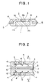
- Fig. 1 is a schematic cross-sectional view showing a first embodiment of a plastic or resin molded type semiconductor device according to the present invention.
- the semiconductor device comprises a semiconductor element 1 in which circuits are formed on the surface of silicon, a chip support 3 tightly fixed onto one surface 1a of the semiconductor element 1 wit an adhesive tape 2, leads 5 respectively electrically connected to A1 pads (bonding pads) formed on the one surface 1a of the semiconductor element 1 through gold wires (bonding wires) 4, and a mold resin 6 that seals the entire semiconductor device.
- the chip support 3 serves so as to reinforce the semiconductor element 1.
- the chip support 3 is provided so as to avoid areas or portions where the gold wires 4 are disposed and extend in the longitudinal direction of the semiconductor element 1 substantially along the center of the semiconductor element 1. Further, the chip support 3 is disposed so as to extend between substantially both ends of the semiconductor element 1.
- a structure is adopted in which the other surface located on the side opposite to one surface of the semiconductor element 1 and a surface of the chip support 3 located on the side opposite to a surface of the chip support 3, which is bonded to the semiconductor element 1, are respectively exposed and sealed with the mold resin 6.
- the chip support 3 is tightly disposed and fixed onto the semiconductor element 1 supported by an unillustrated support with the adhesive tape 2 interposed therebetween.
- the semiconductor element 1 and the chip support 3 are fixed to each other with an adhesive or an adhesive tape.
- the time required to dry the adhesive is spent when they are fixed to each other with the adhesive.
- drying becomes unnecessary.
- the unillustrated A1 pads formed on the semiconductor element 1 and the leads 5 are respectively electrically bonded to one another by the gold wires 4.
- the resin molded type semiconductor device can be obtained by cutting and bending the leads 5 which project from the mold resin 6.
- the other surface 1b located on the side opposite to one surface 1a of the semiconductor element 1 and the surface 3b of the chip support 3 located on the side opposite to the surface 3a of the chip support 3, which is bonded to the semiconductor element 1, are exposed and sealed with the mold resin 6. Therefore, the thickness of a package can be reduced to a size obtained by simply adding the thicknesses of the semiconductor element 1, the adhesive tape 2 and the chip support 3 together, thereby making it possible to thin the semiconductor device. Since the distribution of the mold resin 6 is averaged, warpage of the semiconductor device, which occurs due to heat shrinkage, is hardly generated and the stress applied to the incorporated semiconductor element 1 can be also reduced.
- Figs. 2 and 3 illustrate a second embodiment of a resin molded type semiconductor device according to the present invention.
- Fig. 2 is a fragmentary plan view of the second embodiment.
- Fig. 3 is a schematic enlarged sectional view taken along line A - A of Fig. 2.
- elements of structure indicated by reference numerals identical to those shown in Fig. 1 show the same ones as those shown in Fig. 1.
- the unillustrated A1 pads formed on the semiconductor element 1 and the leads 5 are then electrically bonded to each other by the gold wires 4.
- the mold resin 6 is injected with a part in the interval x , which is unfilled with the adhesive 7 as a mold injection port.
- the entire semiconductor device from which parts of the leads 5 are eliminated, is sealed with the mold resin 6.
- the mold resin 6 flows into the upper side of the adhesive 7 already charged into the interval x and hence the pair of chip supports 3 and 3 and the semiconductor element 1 are brought into a bonded state.
- a final resin molded type semiconductor device is obtained by finally effecting cutting/bending processing on the leads 5 that project from the mold resin 6.
- the mold resin 6 since the structure is adopted wherein the mold resin 6 is injected with the part in the interval x unfilled with the adhesive 7 as the mold injection port and the entire semiconductor device from which the parts of the leads 5 are eliminated, is sealed with the mold resin 6, the mold resin 6 flows into the upper side of the adhesive 7 already poured into the interval x and hence the pair of chip supports 3 and 3 and the semiconductor element 1 are firmer bonded to one another.
- Fig. 4 is a schematic sectional view of a resin molded type semiconductor device showing one modification of the second embodiment of the present invention.
- elements of structure identified by reference numerals identical to those shown in Figs. 2 and 3 show the same ones as those shown in Figs. 2 and 3.
- the structure of this modification can bring about advantageous effects that the bonding between the pair of chip supports 3 and 3 and the semiconductor element 1 is made firmer, as well as advantageous effects obtained by the structure shown in Figs. 2 and 3.
- Fig. 5 is a fragmentary plan view showing a third embodiment of a resin molded type semiconductor device according to the present invention.
- elements of structure indicated by reference numerals identical to those shown in Figs. 1 through 4 show the same ones as those illustrated in Figs. 1 through 4.
- the semiconductor device includes a semiconductor element 1 in which circuits are formed on the surface of silicon, and a plurality of chip supports 3 tightly placed on one surface of the semiconductor element 1 and fixed thereto with an adhesive 7. Further, the semiconductor device has leads respectively electrically connected to unillustrated A1 pads (bonding pads) formed on one side or surface of the semiconductor element 1 through gold wires (bonding wires). Furthermore, the entire semiconductor device is constructed so as to be sealed with a mold resin 6.
- adhesive injection holes 8 are respectively defined in tips of the chip supports 3.
- the individual chip supports 3 are tightly placed on one surface 1a of the semiconductor element 1. Further, the adhesive 7 is injected through the adhesive injection holes 8 so as to bond between the chip supports 3 and the semiconductor element 1.
- the chip supports 3 serve as reinforcing materials for the semiconductor element 1.
- a structure is adopted in which the other surface 1b located on the side opposite to one surface 1a of the semiconductor element 1 and a surface 3b of each chip support 3 located on the side opposite to a surface 3a thereof bonded to the semiconductor element 1, are respectively exposed and sealed with the mold resin 6.
- the other surface 1b located on the side opposite to one surface 1a of the semiconductor element 1 and the surface 3b of each chip support 3 located on the side opposite to the surface 3a thereof bonded to the semiconductor element 1, are exposed and sealed with the mold resin 6. Therefore, the thickness of a package can be reduced to a size obtained by simply adding the thicknesses of the semiconductor element 1 and the chip supports 3 together, thereby making it possible to thin the semiconductor device. Since the mold resin 6 is distributed on the average, warpage of the semiconductor device, which occurs due to heat shrinkage, is hardly produced and the stress applied to the incorporated semiconductor element 1 can be also reduced.
- Fig. 6 is a schematic sectional view of a resin molded type semiconductor device shown as one modification of the third embodiment according to the present invention.
- elements of structure indicated by reference numerals identical to those shown in Figs. 1 through 5 show the same ones as those shown in Figs. 1 through 5.
- chip supports 3 having adhesive injection holes 8 defined in tips thereof extend from the four corners (substantially symmetrical as seen from left to right side although only about the half of the semiconductor device is shown in Fig. 6) of a semiconductor element 1 so as to avoid areas or portions where gold wires (not shown) are provided.
- the chip supports 3 are bonded to one surface 1a of the semiconductor element 1 with an adhesive 7 injected through adhesive injection holes 8.
- the present embodiment is identical in structure to the third embodiment in that the chip supports 3 are used as reinforcing materials for the semiconductor element 1 and other features exist.
- Figs. 7 and 8 show a fourth embodiment of a resin molded type semiconductor device according to the present invention.
- Fig. 7 is a schematic vertical sectional side view of the fourth embodiment.
- Fig. 8 is a schematic horizontal sectional view of the fourth embodiment.
- elements of structure indicated by reference numerals identical to those shown in Figs. 1 through 6 show the same ones as those shown in Figs. 1 through 6.
- Fig. 10 illustrates a fifth embodiment of a resin molded type semiconductor device according to the present invention.
- Fig. 10 is a schematic horizontal sectional view of the fifth embodiment.
- elements of structure designated at reference numerals identical to those shown in Figs. 1 through 9 show the same ones as those shown in Figs. 1 through 9.
- the semiconductor device is of a semiconductor device having a LOC (Lead On Chip) structure.
- the semiconductor device comprises a semiconductor element 1 in which circuits are formed on the surface of silicon, a plurality of leads 5 which are tightly placed on one surface 1a of the semiconductor element 1 with adhesive injection holes 10 defined in tips thereof and are respectively fixed onto the whole surface of the semiconductor element 1 with an adhesive 7 injected into the adhesive injection holes 10, gold wires (bonding wires) for respectively connecting A1 pads (bonding pads) formed on one side of the semiconductor element 1 and the leads 5 to one another, and a mold resin 6 that seals the entire semiconductor device.
- the leads 5 tightly stuck to the semiconductor element 1 serve as for reinforcement.
Landscapes
- Engineering & Computer Science (AREA)
- Physics & Mathematics (AREA)
- Condensed Matter Physics & Semiconductors (AREA)
- General Physics & Mathematics (AREA)
- Computer Hardware Design (AREA)
- Microelectronics & Electronic Packaging (AREA)
- Power Engineering (AREA)
- Manufacturing & Machinery (AREA)
- Structures Or Materials For Encapsulating Or Coating Semiconductor Devices Or Solid State Devices (AREA)
- Encapsulation Of And Coatings For Semiconductor Or Solid State Devices (AREA)
Abstract
Description
- This invention relates to a structure of a resin molded type semiconductor device.
- An IC card and a memory card have been rapidly developed in recent years. With its rapid development, there has been a demand for a thin plastic or resin molded type semiconductor device mounted in the IC or memory card. A vast number of methods of making the resin molded type semiconductor device thinner have been also proposed. As one of the methods, there is known a structure of a semiconductor device disclosed in Japanese Patent Application Laid-Open No. 4-317360, for example, wherein lower surfaces of die pads are exposed without being covered with a mold resin. According to the above structure, the semiconductor device can be made thin by a thickness ranging from about 0.2mm to 0.3mm if the entire thickness of a package is regarded as about 1.0mm.
- An object of the present invention is to cheaply provide a structure of a semiconductor device capable of preventing resin cracks from occurring, providing high reliability and making it thinner.
- According to one aspect of the invention, for achieving the above object, there is provided a structure of a resin molded type semiconductor device, comprising:
- a semiconductor element having a surface to which gold wires are connected;
- a chip support fixed to the semiconductor element so as to avoid portions of the semiconductor element, which are respectively connected with the gold wires; and
- a mold resin for sealing a back surface of the semiconductor element, which is located on the opposite side of the surface of the semiconductor element and a surface of the chip support, which is located on the side opposite to a surface thereof fixed to the semiconductor element, so as to expose both surfaces.
- While the specification concludes with claims particularly pointing out and distinctly claiming the subject matter which is regarded as the invention, it is believed that the invention, the objects, features and advantages thereof will be better understood from the following description taken in connection with the accompanying drawings in which:
- Fig. 1 is a vertical sectional side view of a resin molded type semiconductor device showing a first embodiment of the present invention;
- Fig. 2 is a fragmentary plan view of a resin molded type semiconductor device illustrating a second embodiment of the present invention;
- Fig. 3 is an enlarged vertical sectional side view taken along line A - A of Fig. 2;
- Fig. 4 is a vertical sectional side view depicting a modification of the second embodiment of the present invention;
- Fig. 5 is a fragmentary plan view of a resin molded type semiconductor device depicting a third embodiment of the present invention;
- Fig. 6 is a vertical sectional side view illustrating a modification of the third embodiment of the present invention;
- Fig. 7 is a vertical sectional side view of a resin molded type semiconductor device showing a fourth embodiment of the present invention;
- Fig. 8 is a horizontal sectional view showing the resin molded type semiconductor device according to the fourth embodiment;
- Fig. 9 is a horizontal side view illustrating a modification of the fourth embodiment of the present invention;
- Fig. 10 is a horizontal sectional view of a resin molded type semiconductor device illustrating a fifth embodiment of the present invention;
- Fig. 11 is a sectional view of a resin molded type semiconductor device illustrating a sixth embodiment of the present invention;
- Fig. 12 is a sectional view of a resin molded type semiconductor device showing a seventh embodiment of the present invention;
- Fig. 13 is a sectional view of a resin molded type semiconductor device depicting an eighth embodiment of the present invention;
- Fig. 14 is a fragmentary plan view of a resin molded type semiconductor device showing a ninth embodiment of the present invention;
- Fig. 15 is an enlarged vertical sectional side view taken along line A - A of Fig. 14; and
- Fig. 16 is a sectional view of a resin molded type semiconductor device illustrating a tenth embodiment of the present invention.
- Preferred embodiments of the present invention will hereinafter be described in detail with reference to the accompanying drawings.
- Fig. 1 is a schematic cross-sectional view showing a first embodiment of a plastic or resin molded type semiconductor device according to the present invention. In Fig. 1, the semiconductor device comprises a semiconductor element 1 in which circuits are formed on the surface of silicon, a
chip support 3 tightly fixed onto one surface 1a of the semiconductor element 1 wit anadhesive tape 2, leads 5 respectively electrically connected to A1 pads (bonding pads) formed on the one surface 1a of the semiconductor element 1 through gold wires (bonding wires) 4, and amold resin 6 that seals the entire semiconductor device. Thechip support 3 serves so as to reinforce the semiconductor element 1. - In this type of structure, the
chip support 3 is provided so as to avoid areas or portions where thegold wires 4 are disposed and extend in the longitudinal direction of the semiconductor element 1 substantially along the center of the semiconductor element 1. Further, thechip support 3 is disposed so as to extend between substantially both ends of the semiconductor element 1. Upon sealing the semiconductor device with themold resin 6, a structure is adopted in which the other surface located on the side opposite to one surface of the semiconductor element 1 and a surface of thechip support 3 located on the side opposite to a surface of thechip support 3, which is bonded to the semiconductor element 1, are respectively exposed and sealed with themold resin 6. - A method of manufacturing the resin molded type semiconductor device shown in Fig. 1 will now be described. The
chip support 3 is tightly disposed and fixed onto the semiconductor element 1 supported by an unillustrated support with theadhesive tape 2 interposed therebetween. In this case, the semiconductor element 1 and thechip support 3 are fixed to each other with an adhesive or an adhesive tape. The time required to dry the adhesive is spent when they are fixed to each other with the adhesive. On the other hand, when they are fixed to one another with theadhesive tape 2, drying becomes unnecessary. - Next, the unillustrated A1 pads formed on the semiconductor element 1 and the
leads 5 are respectively electrically bonded to one another by thegold wires 4. - Thereafter, the entire semiconductor device from which parts of the
leads 5 are eliminated, is sealed with themold resin 6. - Finally, the resin molded type semiconductor device can be obtained by cutting and bending the
leads 5 which project from themold resin 6. - Thus, in the resin molded type semiconductor device showing the first embodiment of the present invention, the other surface 1b located on the side opposite to one surface 1a of the semiconductor element 1 and the
surface 3b of thechip support 3 located on the side opposite to thesurface 3a of thechip support 3, which is bonded to the semiconductor element 1, are exposed and sealed with themold resin 6. Therefore, the thickness of a package can be reduced to a size obtained by simply adding the thicknesses of the semiconductor element 1, theadhesive tape 2 and the chip support 3 together, thereby making it possible to thin the semiconductor device. Since the distribution of themold resin 6 is averaged, warpage of the semiconductor device, which occurs due to heat shrinkage, is hardly generated and the stress applied to the incorporated semiconductor element 1 can be also reduced. - Figs. 2 and 3 illustrate a second embodiment of a resin molded type semiconductor device according to the present invention. Fig. 2 is a fragmentary plan view of the second embodiment. Fig. 3 is a schematic enlarged sectional view taken along line A - A of Fig. 2. In Figs. 2 and 3, elements of structure indicated by reference numerals identical to those shown in Fig. 1 show the same ones as those shown in Fig. 1.
- The semiconductor device comprises a semiconductor element 1 in which circuits are formed on the surface of silicon, a pair of chip supports 3 and 3 stuck fast to one surface of the semiconductor element 1 and fixed thereto with an adhesive 7, leads 5 respectively electrically connected to A1 pads (bonding pads) formed on one surface of the semiconductor element 1 through gold wires (bonding wires) 4, and a
mold resin 6 that seals the entire semiconductor device. The pair of chip supports 3 and 3 serves so as to reinforce the semiconductor element 1. - In this type of structure, an interval x is defined between the pair of chip supports 3 and 3. The chip supports 3 and 3 are provided so as to avoid areas or portions where the
gold wires 3 are disposed, and extend in the longitudinal direction of the semiconductor element 1 substantially along the center of the semiconductor element 1. Further, the pair of chip supports 3 and 3, and the pair of chip supports 3 and 3 and the semiconductor element 1 are respectively fixed to one another with theadhesive 7 injected into the interval x. Upon sealing the semiconductor device with themold resin 6, a structure is adopted wherein the other surface 1b located on the side opposite to one surface 1a of the semiconductor element 1 and asurface 3b located on the side opposite to asurface 3a of thechip support 3, which is bonded to the semiconductor element 1, are respectively exposed and sealed with themold resin 6. - A method of manufacturing the resin molded type semiconductor device shown in Figs. 2 and 3 will further be described. Firstly, the
chip supports 3 are tightly placed on the semiconductor element 1 supported by an unillustrated support and are arranged in parallel to each other with the interval x defined therebetween. - Next, parts of both ends extending in the longitudinal direction of the semiconductor element 1 are left and the interval x is filled up with the
adhesive 7. Thus, the pair of chip supports 3 and 3 and the semiconductor element 1 are brought into a tacked state. - The unillustrated A1 pads formed on the semiconductor element 1 and the
leads 5 are then electrically bonded to each other by thegold wires 4. - Thereafter, the
mold resin 6 is injected with a part in the interval x, which is unfilled with the adhesive 7 as a mold injection port. Thus, the entire semiconductor device from which parts of theleads 5 are eliminated, is sealed with themold resin 6. In this case, themold resin 6 flows into the upper side of the adhesive 7 already charged into the interval x and hence the pair of chip supports 3 and 3 and the semiconductor element 1 are brought into a bonded state. - A final resin molded type semiconductor device is obtained by finally effecting cutting/bending processing on the
leads 5 that project from themold resin 6. - Thus, in the resin molded type semiconductor device showing the second embodiment of the present invention, the other surface 1b located on the side opposite to one surface 1a of the semiconductor element 1 and the
surface 3b of thechip support 3 located on the side opposite to thesurface 3a of thechip support 3, which is bonded to the semiconductor element 1, are exposed and sealed with themold resin 6. Therefore, the thickness of a package can be reduced to a size obtained by simply adding the thicknesses of the semiconductor element 1 and thechip support 3 together, thereby making it possible to thin the semiconductor device. Since the distribution of themold resin 6 is averaged, warpage of the semiconductor device, which occurs due to heat shrinkage, is hardly generated and the stress applied to the incorporated semiconductor element 1 can be also reduced. - Further, since the structure is adopted wherein the
mold resin 6 is injected with the part in the interval x unfilled with the adhesive 7 as the mold injection port and the entire semiconductor device from which the parts of theleads 5 are eliminated, is sealed with themold resin 6, themold resin 6 flows into the upper side of the adhesive 7 already poured into the interval x and hence the pair of chip supports 3 and 3 and the semiconductor element 1 are firmer bonded to one another. - Fig. 4 is a schematic sectional view of a resin molded type semiconductor device showing one modification of the second embodiment of the present invention. In Fig. 4, elements of structure identified by reference numerals identical to those shown in Figs. 2 and 3 show the same ones as those shown in Figs. 2 and 3.
- In the illustrated modification, chip supports 3 and 3 provided in a pair have cut-away portions respectively. Further, the chip supports 3 respectively have horizontal and
vertical portions horizontal portions 3A are opposed to each other. Further, an interval is defined between eachhorizontal portion 3A and the semiconductor element 1 so as to be filled with an adhesive 7 and amold resin 6, so that an area that contributes to bonding, is increased. - Thus, the structure of this modification can bring about advantageous effects that the bonding between the pair of chip supports 3 and 3 and the semiconductor element 1 is made firmer, as well as advantageous effects obtained by the structure shown in Figs. 2 and 3.
- Fig. 5 is a fragmentary plan view showing a third embodiment of a resin molded type semiconductor device according to the present invention. In Fig. 5, elements of structure indicated by reference numerals identical to those shown in Figs. 1 through 4 show the same ones as those illustrated in Figs. 1 through 4.
- The semiconductor device includes a semiconductor element 1 in which circuits are formed on the surface of silicon, and a plurality of chip supports 3 tightly placed on one surface of the semiconductor element 1 and fixed thereto with an adhesive 7. Further, the semiconductor device has leads respectively electrically connected to unillustrated A1 pads (bonding pads) formed on one side or surface of the semiconductor element 1 through gold wires (bonding wires). Furthermore, the entire semiconductor device is constructed so as to be sealed with a
mold resin 6. - In this structure,
adhesive injection holes 8 are respectively defined in tips of the chip supports 3. The individual chip supports 3 are tightly placed on one surface 1a of the semiconductor element 1. Further, the adhesive 7 is injected through theadhesive injection holes 8 so as to bond between the chip supports 3 and the semiconductor element 1. The chip supports 3 serve as reinforcing materials for the semiconductor element 1. Upon sealing the semiconductor device with themold resin 6, a structure is adopted in which the other surface 1b located on the side opposite to one surface 1a of the semiconductor element 1 and asurface 3b of eachchip support 3 located on the side opposite to asurface 3a thereof bonded to the semiconductor element 1, are respectively exposed and sealed with themold resin 6. - Thus, in the resin molded type semiconductor device showing the third embodiment of the present invention, the other surface 1b located on the side opposite to one surface 1a of the semiconductor element 1 and the
surface 3b of eachchip support 3 located on the side opposite to thesurface 3a thereof bonded to the semiconductor element 1, are exposed and sealed with themold resin 6. Therefore, the thickness of a package can be reduced to a size obtained by simply adding the thicknesses of the semiconductor element 1 and the chip supports 3 together, thereby making it possible to thin the semiconductor device. Since themold resin 6 is distributed on the average, warpage of the semiconductor device, which occurs due to heat shrinkage, is hardly produced and the stress applied to the incorporated semiconductor element 1 can be also reduced. - Fig. 6 is a schematic sectional view of a resin molded type semiconductor device shown as one modification of the third embodiment according to the present invention. In Fig. 6, elements of structure indicated by reference numerals identical to those shown in Figs. 1 through 5 show the same ones as those shown in Figs. 1 through 5.
- In the illustrated modification, chip supports 3 having
adhesive injection holes 8 defined in tips thereof extend from the four corners (substantially symmetrical as seen from left to right side although only about the half of the semiconductor device is shown in Fig. 6) of a semiconductor element 1 so as to avoid areas or portions where gold wires (not shown) are provided. The chip supports 3 are bonded to one surface 1a of the semiconductor element 1 with an adhesive 7 injected through adhesive injection holes 8. The present embodiment is identical in structure to the third embodiment in that the chip supports 3 are used as reinforcing materials for the semiconductor element 1 and other features exist. - Figs. 7 and 8 show a fourth embodiment of a resin molded type semiconductor device according to the present invention. Fig. 7 is a schematic vertical sectional side view of the fourth embodiment. Fig. 8 is a schematic horizontal sectional view of the fourth embodiment. In Figs. 7 and 8, elements of structure indicated by reference numerals identical to those shown in Figs. 1 through 6 show the same ones as those shown in Figs. 1 through 6.
- Referring to Figs. 7 and 8, the semiconductor device comprises a semiconductor element 1 in which circuits are formed on the surface of silicon, die
pads 9 divided into three which are tightly placed on the other surface 1b of the semiconductor element 1 and fixed thereto with an adhesive 7, leads 5 respectively electrically connected to A1 pads (bonding pads) formed on one surface of the semiconductor element 1 through gold wires (bonding wires) 4, and amold resin 6 that seals the entire semiconductor device. The three diepads 9 serve so as to reinforce the semiconductor element 1. - In this type of structure, the three die
pads 9 extend in the longitudinal direction of the semiconductor device with intervals x defined therebetween. Further, the three diepads 9 are disposed so as to extend between substantially both ends of the semiconductor element 1. The adhesive 7 poured into the intervals x fix between thedie pads 9 and between thedie pads 9 and the semiconductor element 1. Upon sealing the semiconductor device with themold resin 6, a structure is adopted in which a surface 9b located on the side opposite to a surface 9a of each diepad 9, which is bonded to the semiconductor element 1, is exposed and sealed with themold resin 6. - A method of manufacturing the resin molded type semiconductor device shown in Figs. 7 and 8 will further be described. The semiconductor element 1 is first placed on the three die
pads 9 supported by an unillustrated support and provided in parallel to each other with the intervals x defined therebetween so as to extend across the three diepads 9. Further, the semiconductor element 1 is tightly fixed to thedie pads 9 with the adhesive 7 so as to temporarily affix between thedie pads 9 and the semiconductor 1. - Next, the unillustrated A1 pads formed on the semiconductor element 1 and the
leads 5 are electrically bonded to each other through thegold wires 4. - Thereafter, the intervals x are filled with the
mold resin 6. Thus, the entire semiconductor device from which parts of theleads 5 are eliminated, is sealed with themold resin 6. In this case, themold resin 6 also flows into each interval x defined between the adjacent divideddie pads 9. - The
leads 5 that project from themold resin 6, are finally bent so as to obtain a final resin molded type semiconductor device. - Thus, in the resin molded type semiconductor device shown as the fourth embodiment of the present invention, the other surface of each die
pad 9 provided on the other surface 1b located on the side opposite to one surface 1a of the semiconductor element 1, is exposed and sealed with themold resin 6.
Therefore, the thickness of a package can be reduced, thus making it possible to thin the semiconductor device. Since themold resin 6 is poured into each interval x defined between the adjacent divideddie pads 9 and hence the distribution of themold resin 6 is averaged, warpage of the semiconductor device, which occurs due to heat shrinkage, is hardly generated and the stress applied to the incorporated semiconductor element 1 can be also reduced. - Fig. 9 is a schematic sectional view of a resin molded type semiconductor device showing one modification of the fourth embodiment according to the present invention. In Fig. 9, elements of structure indicated by reference numerals identical to those shown in Figs. 1 through 8 show the same ones as those shown in Figs. 1 through 8.
- In the present modification, die
pads 9 divided into four are used. The four diepads 9 extend from the four corners of a semiconductor element 1 and are bonded to one surface 1b of the semiconductor element 1 with an adhesive 7. In regard to other points, the present modification is identical in structure to the fourth embodiment. - Fig. 10 illustrates a fifth embodiment of a resin molded type semiconductor device according to the present invention. Fig. 10 is a schematic horizontal sectional view of the fifth embodiment. In Fig. 10, elements of structure designated at reference numerals identical to those shown in Figs. 1 through 9 show the same ones as those shown in Figs. 1 through 9.
- Referring to Fig. 10, the semiconductor device is of a semiconductor device having a LOC (Lead On Chip) structure. The semiconductor device comprises a semiconductor element 1 in which circuits are formed on the surface of silicon, a plurality of
leads 5 which are tightly placed on one surface 1a of the semiconductor element 1 with adhesive injection holes 10 defined in tips thereof and are respectively fixed onto the whole surface of the semiconductor element 1 with an adhesive 7 injected into the adhesive injection holes 10, gold wires (bonding wires) for respectively connecting A1 pads (bonding pads) formed on one side of the semiconductor element 1 and theleads 5 to one another, and amold resin 6 that seals the entire semiconductor device. The leads 5 tightly stuck to the semiconductor element 1 serve as for reinforcement. - A method of fabricating the resin molded type semiconductor device shown in Fig. 10 will be further described. The leads 5 are first located in predetermined positions of one surface 1a of the semiconductor element 1 and the adhesive 7 is injected through the adhesive injection holes 10 so as to temporarily affix the semiconductor element 1 and the
leads 5. Next, the unillustrated A1 pads formed on the semiconductor element 1 and theleads 5 are electrically bonded to one another by thegold wires 4. - Thereafter, the
mold resin 6 is poured so as to seal the entire semiconductor device from which parts of theleads 5 are excluded. - Finally, the
leads 5 that project from themold resin 6, are cut and bent so as to obtain a final resin molded type semiconductor device. - Thus, since the resin molded type semiconductor device shown as the fifth embodiment has a structure in which the
leads 5 having the adhesive injection holes 10 respectively defined in the tips thereof are tightly placed on one surface 1a of the semiconductor element 1, the semiconductor element 1 and theleads 5 are bonded to one another with the adhesive 7 poured through the adhesive injection holes 10 and thereafter the semiconductor device is sealed with themold resin 6, the electrical connection between the semiconductor element 1 and theleads 5 can be made without using an adhesive tape and hence the cost of processing the adhesive tape can be reduced. - Fig. 11 is a schematic enlarged sectional view showing a sixth embodiment of a resin molded type semiconductor device according to the present invention. In Fig. 11, elements of structure indicated by reference numerals identical to those shown in Fig. 1 show the same ones as those shown in Fig. 1.
- In the sixth embodiment, a projection is formed on the surface of the
chip support 3 opposite to the surface thereof bonded to the chip, which is bonded to the upper surface of the semiconductor element 1 employed in the first embodiment. Fig. 11 shows the case where achip support 63 having a convex cross-section is used as one example of the projection. A method of fabricating the resin molded type semiconductor device according to the sixth embodiment is identical to the method of manufacturing the semiconductor device according to the first embodiment. A convex sectional form of thechip support 63 can be formed by effecting halfetching on the same chip support as that employed in the first embodiment. Owing to the shaping of the cross-section of the chip support in the form of the convex, an interface surface between the chip support and a mold resin can be made longer and the adhesion therebetween can be improved when the semiconductor element 1 and thechip support 63 are sealed with the mold resin. It is therefore possible to prevent moisture from entering from the outside. - Figs. 12 and 13 are respectively schematic enlarged sectional views showing seventh and eighth embodiments of resin molded type semiconductor devices according to the present invention. In Figs. 12 and 13, elements of structure indicated by reference numerals identical to those shown in Fig. 1 show the same ones as those shown in Fig. 1.
- The seventh embodiment shown in Fig. 12 is identical in manufacturing method to the first embodiment. As an adhesive for bonding a
chip support 3 formed on an upper surface of a semiconductor element 1 to a semiconductor element 1, a rubber-like adhesive having a Young's modulus of about 10kg/mm is used. The adhesive 11 is formed by being applied to the upper surface of the semiconductor element 1 during a manufacturing operation. In the eighth embodiment shown in Fig. 13, an adhesive 12 is of a tape-like one and is bonded to achip support 3 in advance. The tape-like adhesive 12 also has a Young's modulus of about 10kg/mm in a manner similar to the rubber-like adhesive 11 employed in the seventh embodiment. - When elastic adhesives are used as the adhesives provided between the semiconductor elements 1 and the chip supports 3 as in the case of the seventh and eighth embodiments respectively, the adhesives serve as cushioning materials even if a mold is brought into contact with the reverse side of the
chip support 3 or the semiconductor element 1 upon mold clamping under resin sealing, so that a large force is prevented from applying to the semiconductor element 1 and thechip support 3. It is therefore possible to prevent cracks from occurring in the reverse side of the semiconductor element 1. - Figs. 14 and 15 illustrate a ninth embodiment of a resin molded type semiconductor device according to the present invention. Fig. 14 is a fragmentary plan view of the resin molded type semiconductor device. Fig. 15 is a schematic enlarged sectional view taken along line A - A of Fig. 2. In Figs. 14 and 15, elements of structure indicated by reference numerals identical to those shown in Fig. 1 show the same ones as those shown in Fig. 1.
- In the resin molded type semiconductor device according to the ninth embodiment, a
metal plate 13 is bonded onto an upper surface of a semiconductor element 1. In the ninth embodiment as well, a mold is brought into direct contact with an upper surface of themetal plate 13 and a lower surface of the semiconductor element 1 and interposed therebetween upon mold clamping under resin sealing. Accordingly, the vertical dimension of the mold is substantially determined by themetal plate 13 and the semiconductor element 1. Since themetal plate 13 is provided separately from leads, themetal plate 13 can be formed so as to become thinner than each of leads. It is therefore possible to make the entire semiconductor device thinner. Assuming now that the thickness of themetal plate 13 is 0.1mm, the thickness of anadhesive tape 2 is 0.1mm and the thickness of the semiconductor element 1 is 0.3mm, an ultra-thin semiconductor device whose entire thickness is 0.5mm can be achieved. - Since the
metal plate 13 is independent of the leads, themetal plate 13 can utilize a material different from that used for the leads. The thermal resistance of the semiconductor device can be lowered by using, for example, a high-radiative material such as Cu, Al, Cu/W or the like as the material. - Fig. 16 is a schematic enlarged sectional view illustrating a tenth embodiment of a resin molded type semiconductor device according to the present invention. In Fig. 16, elements of structure indicated by reference numerals identical to those shown in Fig. 1 show the same ones as those shown in Fig. 1.
- The tenth embodiment shown in Fig. 16 is identical in manufacturing method to the first embodiment. However, the form of a
chip support 3 formed on and bonded to an upper surface of a semiconductor element 1 is different from that of thechip support 3 employed in the first embodiment. Namely, thechip support 3 is half-etched and an adhesive tape is provided within a half-etched area thereby to bond thechip support 3 to the semiconductor element 1. By half-etching the portion of thechip support 3, which is bonded to the semiconductor element 1 as described above, the thickness of the entire semiconductor device can be made thin by a thickness corresponding to the amount of halfetching. - While the present invention has been described with reference to the illustrative embodiments, this description is not intended to be construed in a limiting sense. Various modifications of the illustrative embodiments, as well as other embodiments of the invention, will be apparent to those skilled in the art on reference to this description. It is therefore contemplated that the appended claims will cover any such modifications or embodiments as fall within the true scope of the invention.
Claims (13)
- A structure of a resin molded type semiconductor device, comprising:a semiconductor element having a surface to which gold wires are connected;a chip support fixed to the semiconductor element so as to avoid portions of said semiconductor element, which are respectively connected to the gold wires; anda mold resin for sealing a back surface of said semiconductor element, which is located on the opposite side of the surface of said semiconductor element and a surface of said chip support, which is located on the side opposite to a surface thereof fixed to said semiconductor element, so as to expose said both surfaces.
- A structure of a resin molded type semiconductor device, comprising:a semiconductor element having a surface to which gold wires are connected;a pair of chip supports fixed to said semiconductor element so as to avoid portions of said semiconductor element, which are respectively connected to the gold wires;an adhesive injected between said pair of chip supports, for fixing said pair of chip support and said semiconductor element to each other; anda mold resin for sealing a back surface of said semiconductor element, which is located on the opposite side of the surface of said semiconductor element and a surface of said each chip support, which is located on the side opposite to a surface thereof fixed to said semiconductor element, so as to expose said both surfaces.
- A structure according to claim 2, wherein said chip supports are respectively composed of horizontal and vertical portions integrally provided so as to be substantially L-shaped in cross section and are constructed so that tips of the horizontal portions of said chip supports are disposed face-to-face with each other.
- A structure of a resin molded type semiconductor device, comprising:a semiconductor element having a surface to which gold wires are connected;chip supports disposed so as to avoid portions of said semiconductor element, which are connected to the gold wires and to extend from plural directions, said chip supports having a plurality of adhesive injection holes defined in tips thereof so as to vertically extend therethrough and being bonded to said semiconductor element with adhesives injected through the adhesive injection holes; anda mold resin for sealing a back surface of said semiconductor element, which is located on the opposite side of the surface of said semiconductor element and a surface of said each chip support, which is located on the side opposite to a surface thereof bonded to said semiconductor element, so as to expose said both surfaces.
- A structure of a resin molded type semiconductor device, comprising:a semiconductor element having a surface to which gold wires are connected;at least one pair of die pads disposed on a back surface of said semiconductor element, which is opposite to the surface of said semiconductor; anda mold resin injected between said pair of die pads so as to bond between said pair of die pads, said mold resin bonding said pair of die pads and said semiconductor element to one another and sealing surfaces of said die pads, which are located on the side opposite to surfaces thereof bonded to said semiconductor element, so as to expose the opposed surfaces of said die pads.
- A structure of a resin molded type semiconductor device, comprising:a semiconductor element;a plurality of leads respectively having adhesive injection holes defined in tips thereof provided on a surface of said semiconductor element;an adhesive injected through said each adhesive injection hole, for bonding between said semiconductor element and said each lead; anda mold resin for sealing said semiconductor element and said leads.
- A structure of a resin molded type semiconductor device, comprising:a semiconductor element having a surface to which gold wires are connected;a chip support bonded to the surface of said semiconductor element so as to avoid portions of said semiconductor element, which are connected to the gold wires, said chip support having a projection provided on a surface on the opposite side of the bonded surface; anda mold resin for sealing a back surface of said semiconductor element, which is located on the opposite side of the surface of said semiconductor element and a tip of the projection of said chip support so as to expose the back surface thereof and the tip thereof.
- A structure of a resin molded type semiconductor device, comprising:a semiconductor element having a surface to which gold wires are connected;a chip support face-bonded to said semiconductor element with an elastic adhesive layer interposed therebetween so as to avoid portions of said semiconductor element, which are connected to the gold wires; anda mold resin for sealing a back surface of said semiconductor element, which is located on the opposite side of said one surface of said semiconductor element and a surface of said chip support, which is located on the opposite side of a surface thereof bonded to said semiconductor element, so as to expose said both surfaces.
- A structure of a resin molded type semiconductor device, comprising:a semiconductor element having bonding pads formed on a surface thereof;a plurality of inner leads respectively electrically connected to the bonding pads;a metal plate bonded to said semiconductor element so as to avoid the bonding pads provided on the surface of said semiconductor element; anda mold resin for sealing the other surface of said semiconductor element, which is located on the opposite side of the surface of said semiconductor element and a surface of said metal plate, which is located on the opposite side of a surface thereof bonded to said semiconductor element, so as to expose said both surfaces.
- A structure according to claim 9, wherein said metal plate is a radiative metal plate.
- A structure according to claim 10, wherein said radiative metal plate is selected from Cu, Al and Cu/W as a material.
- A structure of a resin molded type semiconductor device, comprising:a semiconductor element having bonding pads formed on a surface thereof;a plurality of inner leads respectively electrically connected to the bonding pads;a chip support thinner in thickness than each of said inner leads bonded to the surface of said semiconductor element so as to avoid the bonding pads; anda mold resin for sealing the other surface of said semiconductor element, which is located on the opposite side of the surface of said semiconductor element and a surface of said chip support, which is located on the opposite side of a surface thereof bonded to said semiconductor element, so as to expose said both surfaces.
- A semiconductor device structure having first and second major opposed substantially planar surfaces between which peripheral side edge portions extend, a semiconductor element (1), a chip support (3), a plurality of leads (5) that are exposed to the exterior of the device, electrical connection wires (4) that provide electrical connections between the leads and pads (A1) on the semiconductor element, and resin molding material which encapsulates the device, wherein the chip support is adhered to the semiconductor element on the same side as the pads, the first major surface includes a surface of the chip support contiguous with a first surface of the resin molding material, and the second major surface includes a surface of the semiconductor element contiguous with a second surface of the resin molding material.
Applications Claiming Priority (2)
| Application Number | Priority Date | Filing Date | Title |
|---|---|---|---|
| JP273262/94 | 1994-11-08 | ||
| JP27326294 | 1994-11-08 |
Publications (2)
| Publication Number | Publication Date |
|---|---|
| EP0712159A2 true EP0712159A2 (en) | 1996-05-15 |
| EP0712159A3 EP0712159A3 (en) | 1997-03-26 |
Family
ID=17525385
Family Applications (1)
| Application Number | Title | Priority Date | Filing Date |
|---|---|---|---|
| EP95307678A Ceased EP0712159A3 (en) | 1994-11-08 | 1995-10-27 | Structure of resin molded type semiconductor |
Country Status (4)
| Country | Link |
|---|---|
| US (1) | US6002181A (en) |
| EP (1) | EP0712159A3 (en) |
| KR (1) | KR100366111B1 (en) |
| TW (1) | TW357443B (en) |
Cited By (2)
| Publication number | Priority date | Publication date | Assignee | Title |
|---|---|---|---|---|
| FR2788882A1 (en) * | 1999-01-27 | 2000-07-28 | Schlumberger Systems & Service | Integrated circuit module for smart card |
| US6340837B1 (en) | 1998-08-31 | 2002-01-22 | Hitachi, Ltd. | Semiconductor device and method of fabricating the same |
Families Citing this family (10)
| Publication number | Priority date | Publication date | Assignee | Title |
|---|---|---|---|---|
| SG60099A1 (en) * | 1996-08-16 | 1999-02-22 | Sony Corp | Semiconductor package and manufacturing method of lead frame |
| US6127724A (en) * | 1996-10-31 | 2000-10-03 | Tessera, Inc. | Packaged microelectronic elements with enhanced thermal conduction |
| US5920112A (en) * | 1998-04-07 | 1999-07-06 | Micro Networks Corporation | Circuit including a corral for containing a protective coating, and method of making same |
| TW429494B (en) * | 1999-11-08 | 2001-04-11 | Siliconware Precision Industries Co Ltd | Quad flat non-leaded package |
| US6559525B2 (en) * | 2000-01-13 | 2003-05-06 | Siliconware Precision Industries Co., Ltd. | Semiconductor package having heat sink at the outer surface |
| TW518729B (en) * | 2001-09-04 | 2003-01-21 | Siliconware Precision Industries Co Ltd | Quad flat non-leaded semiconductor package structure and manufacturing process |
| US20040124508A1 (en) * | 2002-11-27 | 2004-07-01 | United Test And Assembly Test Center Ltd. | High performance chip scale leadframe package and method of manufacturing the package |
| TWI334638B (en) * | 2005-12-30 | 2010-12-11 | Ind Tech Res Inst | Structure and process of chip package |
| US7911040B2 (en) * | 2007-12-27 | 2011-03-22 | Stats Chippac Ltd. | Integrated circuit package with improved connections |
| KR20160038364A (en) * | 2014-09-30 | 2016-04-07 | 현대모비스 주식회사 | Non-insulation type power semiconductor module and Method for manufacturing the same |
Citations (5)
| Publication number | Priority date | Publication date | Assignee | Title |
|---|---|---|---|---|
| JPH01106455A (en) * | 1987-10-19 | 1989-04-24 | Matsushita Electric Ind Co Ltd | Semiconductor integration circuit device |
| JPH0262295A (en) * | 1988-08-29 | 1990-03-02 | Matsushita Electric Ind Co Ltd | Information medium, conveying body therefor and reader thereof |
| JPH04317360A (en) | 1991-04-16 | 1992-11-09 | Sony Corp | Resin sealed semiconductor device |
| JPH0513477A (en) * | 1991-07-01 | 1993-01-22 | Oki Electric Ind Co Ltd | Manufacture of resin-sealed type semiconductor device |
| JPH05315526A (en) * | 1992-05-08 | 1993-11-26 | Hitachi Ltd | Semiconductor device |
Family Cites Families (11)
| Publication number | Priority date | Publication date | Assignee | Title |
|---|---|---|---|---|
| JPH0775253B2 (en) * | 1987-06-30 | 1995-08-09 | 株式会社日立製作所 | Semiconductor device and manufacturing method thereof |
| JP2660732B2 (en) * | 1989-01-09 | 1997-10-08 | 株式会社日立製作所 | Semiconductor device |
| JPH02260558A (en) * | 1989-03-31 | 1990-10-23 | Nec Corp | Lead frame of semiconductor device |
| US5157478A (en) * | 1989-04-19 | 1992-10-20 | Mitsubishi Denki Kabushiki Kaisha | Tape automated bonding packaged semiconductor device incorporating a heat sink |
| JP2875334B2 (en) * | 1990-04-06 | 1999-03-31 | 株式会社日立製作所 | Semiconductor device |
| JPH04245462A (en) * | 1991-01-30 | 1992-09-02 | Hitachi Ltd | Semiconductor integrated circuit device and its manufacture |
| US5173764A (en) * | 1991-04-08 | 1992-12-22 | Motorola, Inc. | Semiconductor device having a particular lid means and encapsulant to reduce die stress |
| JP2970060B2 (en) * | 1991-06-06 | 1999-11-02 | 日本電気株式会社 | Lead frame for resin-sealed semiconductor device |
| US5387554A (en) * | 1992-09-10 | 1995-02-07 | Vlsi Technology, Inc. | Apparatus and method for thermally coupling a heat sink to a lead frame |
| JP2824175B2 (en) * | 1992-09-17 | 1998-11-11 | シャープ株式会社 | Semiconductor device and manufacturing method thereof |
| JP2874483B2 (en) * | 1992-10-05 | 1999-03-24 | 松下電器産業株式会社 | Semiconductor device |
-
1995
- 1995-10-23 KR KR1019950036671A patent/KR100366111B1/en not_active IP Right Cessation
- 1995-10-23 US US08/551,917 patent/US6002181A/en not_active Expired - Fee Related
- 1995-10-26 TW TW084111314A patent/TW357443B/en active
- 1995-10-27 EP EP95307678A patent/EP0712159A3/en not_active Ceased
Patent Citations (5)
| Publication number | Priority date | Publication date | Assignee | Title |
|---|---|---|---|---|
| JPH01106455A (en) * | 1987-10-19 | 1989-04-24 | Matsushita Electric Ind Co Ltd | Semiconductor integration circuit device |
| JPH0262295A (en) * | 1988-08-29 | 1990-03-02 | Matsushita Electric Ind Co Ltd | Information medium, conveying body therefor and reader thereof |
| JPH04317360A (en) | 1991-04-16 | 1992-11-09 | Sony Corp | Resin sealed semiconductor device |
| JPH0513477A (en) * | 1991-07-01 | 1993-01-22 | Oki Electric Ind Co Ltd | Manufacture of resin-sealed type semiconductor device |
| JPH05315526A (en) * | 1992-05-08 | 1993-11-26 | Hitachi Ltd | Semiconductor device |
Cited By (6)
| Publication number | Priority date | Publication date | Assignee | Title |
|---|---|---|---|---|
| US6340837B1 (en) | 1998-08-31 | 2002-01-22 | Hitachi, Ltd. | Semiconductor device and method of fabricating the same |
| US6441400B1 (en) | 1998-08-31 | 2002-08-27 | Hitachi, Ltd. | Semiconductor device and method of fabricating the same |
| US6476479B2 (en) | 1998-08-31 | 2002-11-05 | Hitachi, Ltd. | Semiconductor device and method of fabricating the same |
| FR2788882A1 (en) * | 1999-01-27 | 2000-07-28 | Schlumberger Systems & Service | Integrated circuit module for smart card |
| WO2000045434A1 (en) * | 1999-01-27 | 2000-08-03 | Schlumberger Systemes | Integrated circuit device, electronic module for chip card using said device and method for making same |
| US7208822B1 (en) | 1999-01-27 | 2007-04-24 | Axalto Sa | Integrated circuit device, electronic module for chip cards using said device and method for making same |
Also Published As
| Publication number | Publication date |
|---|---|
| KR960019621A (en) | 1996-06-17 |
| EP0712159A3 (en) | 1997-03-26 |
| TW357443B (en) | 1999-05-01 |
| KR100366111B1 (en) | 2003-03-06 |
| US6002181A (en) | 1999-12-14 |
Similar Documents
| Publication | Publication Date | Title |
|---|---|---|
| KR100776451B1 (en) | Semiconductor device and manufacturing method thereof | |
| US6410979B2 (en) | Ball-grid-array semiconductor device with protruding terminals | |
| JPH0730046A (en) | Semiconductor device, lead frame, and manufacture of semiconductor device | |
| KR100242393B1 (en) | Semiconductor Package and Manufacturing Method | |
| US6002181A (en) | Structure of resin molded type semiconductor device with embedded thermal dissipator | |
| KR100428271B1 (en) | Integrated circuit package and its manufacturing method | |
| EP0807973B1 (en) | Plastic molded type semiconductor device and method of manufacturing the same | |
| US5796160A (en) | Resin-sealed semiconductor device | |
| US5714799A (en) | Resin-sealed type semiconductor device having an unoccupied second die pad | |
| US5952710A (en) | Semiconductor device and method of manufacturing same | |
| JP3367272B2 (en) | Lead frame and semiconductor device | |
| JPH0719859B2 (en) | Method for manufacturing IC card module | |
| JP3229816B2 (en) | Method for manufacturing resin-encapsulated semiconductor device | |
| JPH06342816A (en) | Semiconductor device, its manufacture, and lead frame used therefor | |
| JPH08213513A (en) | Structure of resin-sealed semiconductor device | |
| JP2756436B2 (en) | Semiconductor device and manufacturing method thereof | |
| KR100244254B1 (en) | Lead frame and semiconductor package with such lead frame | |
| KR100304922B1 (en) | Lead frame and semiconductor package with such lead frame | |
| EP1381084A1 (en) | Semiconductor device and method of its fabrication | |
| KR0185571B1 (en) | Chip-on-lead leadframe with chip adhesion stepped at inner lead end and semiconductor chip package using same | |
| JP4620915B2 (en) | Resin-sealed semiconductor device | |
| JPS63120694A (en) | Manufacture of semiconductor device | |
| KR970004618Y1 (en) | Padless Semiconductor Package | |
| KR200141125Y1 (en) | Structure of lead frame | |
| JPH0737921A (en) | Semiconductor device |
Legal Events
| Date | Code | Title | Description |
|---|---|---|---|
| PUAI | Public reference made under article 153(3) epc to a published international application that has entered the european phase |
Free format text: ORIGINAL CODE: 0009012 |
|
| AK | Designated contracting states |
Kind code of ref document: A2 Designated state(s): DE FR GB NL |
|
| PUAL | Search report despatched |
Free format text: ORIGINAL CODE: 0009013 |
|
| AK | Designated contracting states |
Kind code of ref document: A3 Designated state(s): DE FR GB NL |
|
| 17P | Request for examination filed |
Effective date: 19970923 |
|
| 17Q | First examination report despatched |
Effective date: 19990928 |
|
| STAA | Information on the status of an ep patent application or granted ep patent |
Free format text: STATUS: THE APPLICATION HAS BEEN REFUSED |
|
| 18R | Application refused |
Effective date: 20010826 |