EP0473448B1 - Electrophotographic imaging member - Google Patents
Electrophotographic imaging member Download PDFInfo
- Publication number
- EP0473448B1 EP0473448B1 EP91307955A EP91307955A EP0473448B1 EP 0473448 B1 EP0473448 B1 EP 0473448B1 EP 91307955 A EP91307955 A EP 91307955A EP 91307955 A EP91307955 A EP 91307955A EP 0473448 B1 EP0473448 B1 EP 0473448B1
- Authority
- EP
- European Patent Office
- Prior art keywords
- layer
- group
- imaging member
- charge
- nitrogen
- Prior art date
- Legal status (The legal status is an assumption and is not a legal conclusion. Google has not performed a legal analysis and makes no representation as to the accuracy of the status listed.)
- Expired - Lifetime
Links
- 238000003384 imaging method Methods 0.000 title claims description 32
- 239000010410 layer Substances 0.000 claims description 195
- 230000000903 blocking effect Effects 0.000 claims description 62
- -1 amino, imino Chemical group 0.000 claims description 36
- 239000000203 mixture Substances 0.000 claims description 29
- 239000000758 substrate Substances 0.000 claims description 22
- 229910000077 silane Inorganic materials 0.000 claims description 21
- BLRPTPMANUNPDV-UHFFFAOYSA-N Silane Chemical group [SiH4] BLRPTPMANUNPDV-UHFFFAOYSA-N 0.000 claims description 20
- 229910021595 Copper(I) iodide Inorganic materials 0.000 claims description 16
- LSXDOTMGLUJQCM-UHFFFAOYSA-M copper(i) iodide Chemical compound I[Cu] LSXDOTMGLUJQCM-UHFFFAOYSA-M 0.000 claims description 16
- QJGQUHMNIGDVPM-UHFFFAOYSA-N nitrogen group Chemical group [N] QJGQUHMNIGDVPM-UHFFFAOYSA-N 0.000 claims description 15
- 229920000642 polymer Polymers 0.000 claims description 15
- 150000003512 tertiary amines Chemical class 0.000 claims description 13
- 239000012790 adhesive layer Substances 0.000 claims description 12
- 229910052802 copper Inorganic materials 0.000 claims description 12
- 239000010949 copper Substances 0.000 claims description 12
- RYGMFSIKBFXOCR-UHFFFAOYSA-N Copper Chemical compound [Cu] RYGMFSIKBFXOCR-UHFFFAOYSA-N 0.000 claims description 11
- 229910021645 metal ion Inorganic materials 0.000 claims description 11
- WYTZZXDRDKSJID-UHFFFAOYSA-N (3-aminopropyl)triethoxysilane Chemical group CCO[Si](OCC)(OCC)CCCN WYTZZXDRDKSJID-UHFFFAOYSA-N 0.000 claims description 10
- RTAQQCXQSZGOHL-UHFFFAOYSA-N Titanium Chemical compound [Ti] RTAQQCXQSZGOHL-UHFFFAOYSA-N 0.000 claims description 9
- PXHVJJICTQNCMI-UHFFFAOYSA-N Nickel Chemical compound [Ni] PXHVJJICTQNCMI-UHFFFAOYSA-N 0.000 claims description 8
- 229910052723 transition metal Inorganic materials 0.000 claims description 7
- 150000003624 transition metals Chemical class 0.000 claims description 7
- XEEYBQQBJWHFJM-UHFFFAOYSA-N Iron Chemical compound [Fe] XEEYBQQBJWHFJM-UHFFFAOYSA-N 0.000 claims description 6
- KDLHZDBZIXYQEI-UHFFFAOYSA-N Palladium Chemical compound [Pd] KDLHZDBZIXYQEI-UHFFFAOYSA-N 0.000 claims description 6
- BASFCYQUMIYNBI-UHFFFAOYSA-N platinum Chemical compound [Pt] BASFCYQUMIYNBI-UHFFFAOYSA-N 0.000 claims description 6
- 150000003839 salts Chemical class 0.000 claims description 6
- 229910052719 titanium Inorganic materials 0.000 claims description 5
- 239000010936 titanium Substances 0.000 claims description 5
- VYZAMTAEIAYCRO-UHFFFAOYSA-N Chromium Chemical compound [Cr] VYZAMTAEIAYCRO-UHFFFAOYSA-N 0.000 claims description 4
- 229910052804 chromium Inorganic materials 0.000 claims description 4
- 239000011651 chromium Substances 0.000 claims description 4
- 229910017052 cobalt Inorganic materials 0.000 claims description 4
- 239000010941 cobalt Substances 0.000 claims description 4
- GUTLYIVDDKVIGB-UHFFFAOYSA-N cobalt atom Chemical compound [Co] GUTLYIVDDKVIGB-UHFFFAOYSA-N 0.000 claims description 4
- PCHJSUWPFVWCPO-UHFFFAOYSA-N gold Chemical compound [Au] PCHJSUWPFVWCPO-UHFFFAOYSA-N 0.000 claims description 4
- 229910052737 gold Inorganic materials 0.000 claims description 4
- 239000010931 gold Substances 0.000 claims description 4
- 229910052759 nickel Inorganic materials 0.000 claims description 4
- 229910052720 vanadium Inorganic materials 0.000 claims description 4
- 239000005725 8-Hydroxyquinoline Substances 0.000 claims description 3
- KJTLSVCANCCWHF-UHFFFAOYSA-N Ruthenium Chemical compound [Ru] KJTLSVCANCCWHF-UHFFFAOYSA-N 0.000 claims description 3
- BQCADISMDOOEFD-UHFFFAOYSA-N Silver Chemical compound [Ag] BQCADISMDOOEFD-UHFFFAOYSA-N 0.000 claims description 3
- HCHKCACWOHOZIP-UHFFFAOYSA-N Zinc Chemical compound [Zn] HCHKCACWOHOZIP-UHFFFAOYSA-N 0.000 claims description 3
- 229910052793 cadmium Inorganic materials 0.000 claims description 3
- BDOSMKKIYDKNTQ-UHFFFAOYSA-N cadmium atom Chemical compound [Cd] BDOSMKKIYDKNTQ-UHFFFAOYSA-N 0.000 claims description 3
- 229920003020 cross-linked polyethylene Polymers 0.000 claims description 3
- 239000004703 cross-linked polyethylene Substances 0.000 claims description 3
- 150000002466 imines Chemical class 0.000 claims description 3
- 229910052742 iron Inorganic materials 0.000 claims description 3
- WPBNNNQJVZRUHP-UHFFFAOYSA-L manganese(2+);methyl n-[[2-(methoxycarbonylcarbamothioylamino)phenyl]carbamothioyl]carbamate;n-[2-(sulfidocarbothioylamino)ethyl]carbamodithioate Chemical compound [Mn+2].[S-]C(=S)NCCNC([S-])=S.COC(=O)NC(=S)NC1=CC=CC=C1NC(=S)NC(=O)OC WPBNNNQJVZRUHP-UHFFFAOYSA-L 0.000 claims description 3
- QSHDDOUJBYECFT-UHFFFAOYSA-N mercury Chemical compound [Hg] QSHDDOUJBYECFT-UHFFFAOYSA-N 0.000 claims description 3
- 229910052753 mercury Inorganic materials 0.000 claims description 3
- 229910052762 osmium Inorganic materials 0.000 claims description 3
- SYQBFIAQOQZEGI-UHFFFAOYSA-N osmium atom Chemical compound [Os] SYQBFIAQOQZEGI-UHFFFAOYSA-N 0.000 claims description 3
- 229960003540 oxyquinoline Drugs 0.000 claims description 3
- 229910052763 palladium Inorganic materials 0.000 claims description 3
- 229910052697 platinum Inorganic materials 0.000 claims description 3
- MCJGNVYPOGVAJF-UHFFFAOYSA-N quinolin-8-ol Chemical compound C1=CN=C2C(O)=CC=CC2=C1 MCJGNVYPOGVAJF-UHFFFAOYSA-N 0.000 claims description 3
- 229910052703 rhodium Inorganic materials 0.000 claims description 3
- 239000010948 rhodium Substances 0.000 claims description 3
- MHOVAHRLVXNVSD-UHFFFAOYSA-N rhodium atom Chemical compound [Rh] MHOVAHRLVXNVSD-UHFFFAOYSA-N 0.000 claims description 3
- 229910052707 ruthenium Inorganic materials 0.000 claims description 3
- 229910052709 silver Inorganic materials 0.000 claims description 3
- 239000004332 silver Substances 0.000 claims description 3
- 229910052725 zinc Inorganic materials 0.000 claims description 3
- 239000011701 zinc Substances 0.000 claims description 3
- JOZYBUSXAGFNKN-UHFFFAOYSA-N N-pyridin-2-ylpyridin-2-amine Chemical compound N(c1ccccn1)c1ccccn1.N(c1ccccn1)c1ccccn1 JOZYBUSXAGFNKN-UHFFFAOYSA-N 0.000 claims description 2
- 150000004696 coordination complex Chemical class 0.000 claims description 2
- LEONUFNNVUYDNQ-UHFFFAOYSA-N vanadium atom Chemical compound [V] LEONUFNNVUYDNQ-UHFFFAOYSA-N 0.000 claims 2
- 229910052741 iridium Inorganic materials 0.000 claims 1
- GKOZUEZYRPOHIO-UHFFFAOYSA-N iridium atom Chemical compound [Ir] GKOZUEZYRPOHIO-UHFFFAOYSA-N 0.000 claims 1
- 239000000463 material Substances 0.000 description 59
- 239000000243 solution Substances 0.000 description 36
- YMWUJEATGCHHMB-UHFFFAOYSA-N Dichloromethane Chemical compound ClCCl YMWUJEATGCHHMB-UHFFFAOYSA-N 0.000 description 24
- YXFVVABEGXRONW-UHFFFAOYSA-N Toluene Chemical compound CC1=CC=CC=C1 YXFVVABEGXRONW-UHFFFAOYSA-N 0.000 description 22
- 239000011230 binding agent Substances 0.000 description 19
- 108091008695 photoreceptors Proteins 0.000 description 18
- WYURNTSHIVDZCO-UHFFFAOYSA-N Tetrahydrofuran Chemical compound C1CCOC1 WYURNTSHIVDZCO-UHFFFAOYSA-N 0.000 description 16
- 229910052751 metal Inorganic materials 0.000 description 16
- 239000002184 metal Substances 0.000 description 16
- LYCAIKOWRPUZTN-UHFFFAOYSA-N Ethylene glycol Chemical compound OCCO LYCAIKOWRPUZTN-UHFFFAOYSA-N 0.000 description 15
- 125000004432 carbon atom Chemical group C* 0.000 description 15
- 238000000576 coating method Methods 0.000 description 15
- 239000011248 coating agent Substances 0.000 description 14
- 238000000034 method Methods 0.000 description 14
- BUGBHKTXTAQXES-UHFFFAOYSA-N Selenium Chemical compound [Se] BUGBHKTXTAQXES-UHFFFAOYSA-N 0.000 description 13
- 239000007795 chemical reaction product Substances 0.000 description 13
- 229910052711 selenium Inorganic materials 0.000 description 13
- 239000011669 selenium Substances 0.000 description 13
- 125000000217 alkyl group Chemical group 0.000 description 11
- 229920005989 resin Polymers 0.000 description 11
- 239000011347 resin Substances 0.000 description 11
- IJGRMHOSHXDMSA-UHFFFAOYSA-N Atomic nitrogen Chemical compound N#N IJGRMHOSHXDMSA-UHFFFAOYSA-N 0.000 description 10
- LFQSCWFLJHTTHZ-UHFFFAOYSA-N Ethanol Chemical compound CCO LFQSCWFLJHTTHZ-UHFFFAOYSA-N 0.000 description 10
- 229920000728 polyester Polymers 0.000 description 10
- 239000002904 solvent Substances 0.000 description 10
- 239000000049 pigment Substances 0.000 description 9
- XLYOFNOQVPJJNP-UHFFFAOYSA-N water Substances O XLYOFNOQVPJJNP-UHFFFAOYSA-N 0.000 description 9
- UBOXGVDOUJQMTN-UHFFFAOYSA-N 1,1,2-trichloroethane Chemical compound ClCC(Cl)Cl UBOXGVDOUJQMTN-UHFFFAOYSA-N 0.000 description 8
- 238000006243 chemical reaction Methods 0.000 description 8
- OPQARKPSCNTWTJ-UHFFFAOYSA-L copper(ii) acetate Chemical compound [Cu+2].CC([O-])=O.CC([O-])=O OPQARKPSCNTWTJ-UHFFFAOYSA-L 0.000 description 8
- 229910052757 nitrogen Inorganic materials 0.000 description 8
- YLQBMQCUIZJEEH-UHFFFAOYSA-N tetrahydrofuran Natural products C=1C=COC=1 YLQBMQCUIZJEEH-UHFFFAOYSA-N 0.000 description 8
- 229920001634 Copolyester Polymers 0.000 description 7
- 238000002347 injection Methods 0.000 description 7
- 239000007924 injection Substances 0.000 description 7
- 229920005668 polycarbonate resin Polymers 0.000 description 7
- 239000004431 polycarbonate resin Substances 0.000 description 7
- 150000004756 silanes Chemical class 0.000 description 7
- OGGKVJMNFFSDEV-UHFFFAOYSA-N 3-methyl-n-[4-[4-(n-(3-methylphenyl)anilino)phenyl]phenyl]-n-phenylaniline Chemical compound CC1=CC=CC(N(C=2C=CC=CC=2)C=2C=CC(=CC=2)C=2C=CC(=CC=2)N(C=2C=CC=CC=2)C=2C=C(C)C=CC=2)=C1 OGGKVJMNFFSDEV-UHFFFAOYSA-N 0.000 description 6
- KKEYFWRCBNTPAC-UHFFFAOYSA-N Terephthalic acid Chemical compound OC(=O)C1=CC=C(C(O)=O)C=C1 KKEYFWRCBNTPAC-UHFFFAOYSA-N 0.000 description 6
- 230000002411 adverse Effects 0.000 description 6
- 238000001035 drying Methods 0.000 description 6
- QQVIHTHCMHWDBS-UHFFFAOYSA-N isophthalic acid Chemical compound OC(=O)C1=CC=CC(C(O)=O)=C1 QQVIHTHCMHWDBS-UHFFFAOYSA-N 0.000 description 6
- 229920000515 polycarbonate Polymers 0.000 description 6
- 239000000126 substance Substances 0.000 description 6
- 239000000853 adhesive Substances 0.000 description 5
- 230000001070 adhesive effect Effects 0.000 description 5
- 230000001351 cycling effect Effects 0.000 description 5
- KPUWHANPEXNPJT-UHFFFAOYSA-N disiloxane Chemical class [SiH3]O[SiH3] KPUWHANPEXNPJT-UHFFFAOYSA-N 0.000 description 5
- 230000007062 hydrolysis Effects 0.000 description 5
- 238000006460 hydrolysis reaction Methods 0.000 description 5
- 239000002245 particle Substances 0.000 description 5
- 229920003227 poly(N-vinyl carbazole) Polymers 0.000 description 5
- 239000007921 spray Substances 0.000 description 5
- 238000005507 spraying Methods 0.000 description 5
- 125000004429 atom Chemical group 0.000 description 4
- 230000000052 comparative effect Effects 0.000 description 4
- 230000000536 complexating effect Effects 0.000 description 4
- 150000001875 compounds Chemical class 0.000 description 4
- JHIVVAPYMSGYDF-UHFFFAOYSA-N cyclohexanone Chemical compound O=C1CCCCC1 JHIVVAPYMSGYDF-UHFFFAOYSA-N 0.000 description 4
- 125000001449 isopropyl group Chemical group [H]C([H])([H])C([H])(*)C([H])([H])[H] 0.000 description 4
- 150000002739 metals Chemical class 0.000 description 4
- YRZZLAGRKZIJJI-UHFFFAOYSA-N oxyvanadium phthalocyanine Chemical compound [V+2]=O.C12=CC=CC=C2C(N=C2[N-]C(C3=CC=CC=C32)=N2)=NC1=NC([C]1C=CC=CC1=1)=NC=1N=C1[C]3C=CC=CC3=C2[N-]1 YRZZLAGRKZIJJI-UHFFFAOYSA-N 0.000 description 4
- IEQIEDJGQAUEQZ-UHFFFAOYSA-N phthalocyanine Chemical compound N1C(N=C2C3=CC=CC=C3C(N=C3C4=CC=CC=C4C(=N4)N3)=N2)=C(C=CC=C2)C2=C1N=C1C2=CC=CC=C2C4=N1 IEQIEDJGQAUEQZ-UHFFFAOYSA-N 0.000 description 4
- 229920006267 polyester film Polymers 0.000 description 4
- 125000002924 primary amino group Chemical group [H]N([H])* 0.000 description 4
- 230000035484 reaction time Effects 0.000 description 4
- QTBSBXVTEAMEQO-UHFFFAOYSA-N Acetic acid Chemical compound CC(O)=O QTBSBXVTEAMEQO-UHFFFAOYSA-N 0.000 description 3
- 239000004425 Makrolon Substances 0.000 description 3
- 150000008043 acidic salts Chemical class 0.000 description 3
- 150000004982 aromatic amines Chemical class 0.000 description 3
- KRKNYBCHXYNGOX-UHFFFAOYSA-N citric acid Chemical compound OC(=O)CC(O)(C(O)=O)CC(O)=O KRKNYBCHXYNGOX-UHFFFAOYSA-N 0.000 description 3
- 239000004020 conductor Substances 0.000 description 3
- 238000004132 cross linking Methods 0.000 description 3
- 229940076286 cupric acetate Drugs 0.000 description 3
- 238000000151 deposition Methods 0.000 description 3
- 150000002009 diols Chemical class 0.000 description 3
- 230000009477 glass transition Effects 0.000 description 3
- 230000005525 hole transport Effects 0.000 description 3
- 125000001841 imino group Chemical group [H]N=* 0.000 description 3
- 230000003993 interaction Effects 0.000 description 3
- 125000001997 phenyl group Chemical group [H]C1=C([H])C([H])=C(*)C([H])=C1[H] 0.000 description 3
- 239000004417 polycarbonate Substances 0.000 description 3
- 230000005855 radiation Effects 0.000 description 3
- 239000002002 slurry Substances 0.000 description 3
- UOCLXMDMGBRAIB-UHFFFAOYSA-N 1,1,1-trichloroethane Chemical compound CC(Cl)(Cl)Cl UOCLXMDMGBRAIB-UHFFFAOYSA-N 0.000 description 2
- KIIFVSJBFGYDFV-UHFFFAOYSA-N 1h-benzimidazole;perylene Chemical group C1=CC=C2NC=NC2=C1.C1=CC(C2=CC=CC=3C2=C2C=CC=3)=C3C2=CC=CC3=C1 KIIFVSJBFGYDFV-UHFFFAOYSA-N 0.000 description 2
- SJECZPVISLOESU-UHFFFAOYSA-N 3-trimethoxysilylpropan-1-amine Chemical compound CO[Si](OC)(OC)CCCN SJECZPVISLOESU-UHFFFAOYSA-N 0.000 description 2
- NLXLAEXVIDQMFP-UHFFFAOYSA-N Ammonia chloride Chemical compound [NH4+].[Cl-] NLXLAEXVIDQMFP-UHFFFAOYSA-N 0.000 description 2
- 229920002799 BoPET Polymers 0.000 description 2
- KFZMGEQAYNKOFK-UHFFFAOYSA-N Isopropanol Chemical compound CC(C)O KFZMGEQAYNKOFK-UHFFFAOYSA-N 0.000 description 2
- 239000005041 Mylar™ Substances 0.000 description 2
- NBIIXXVUZAFLBC-UHFFFAOYSA-N Phosphoric acid Chemical compound OP(O)(O)=O NBIIXXVUZAFLBC-UHFFFAOYSA-N 0.000 description 2
- 239000004721 Polyphenylene oxide Substances 0.000 description 2
- NRCMAYZCPIVABH-UHFFFAOYSA-N Quinacridone Chemical compound N1C2=CC=CC=C2C(=O)C2=C1C=C1C(=O)C3=CC=CC=C3NC1=C2 NRCMAYZCPIVABH-UHFFFAOYSA-N 0.000 description 2
- 229910001370 Se alloy Inorganic materials 0.000 description 2
- XSTXAVWGXDQKEL-UHFFFAOYSA-N Trichloroethylene Chemical group ClC=C(Cl)Cl XSTXAVWGXDQKEL-UHFFFAOYSA-N 0.000 description 2
- 239000002253 acid Substances 0.000 description 2
- 230000003213 activating effect Effects 0.000 description 2
- WNLRTRBMVRJNCN-UHFFFAOYSA-N adipic acid Chemical compound OC(=O)CCCCC(O)=O WNLRTRBMVRJNCN-UHFFFAOYSA-N 0.000 description 2
- 125000003545 alkoxy group Chemical group 0.000 description 2
- 125000001118 alkylidene group Chemical group 0.000 description 2
- 150000001412 amines Chemical class 0.000 description 2
- 229910052785 arsenic Inorganic materials 0.000 description 2
- 125000003118 aryl group Chemical group 0.000 description 2
- 230000015572 biosynthetic process Effects 0.000 description 2
- 230000009920 chelation Effects 0.000 description 2
- 239000002131 composite material Substances 0.000 description 2
- 238000007796 conventional method Methods 0.000 description 2
- 230000002939 deleterious effect Effects 0.000 description 2
- 238000003618 dip coating Methods 0.000 description 2
- ZUOUZKKEUPVFJK-UHFFFAOYSA-N diphenyl Chemical group C1=CC=CC=C1C1=CC=CC=C1 ZUOUZKKEUPVFJK-UHFFFAOYSA-N 0.000 description 2
- 239000006185 dispersion Substances 0.000 description 2
- 125000006575 electron-withdrawing group Chemical group 0.000 description 2
- 229910052739 hydrogen Inorganic materials 0.000 description 2
- BDAGIHXWWSANSR-UHFFFAOYSA-N methanoic acid Natural products OC=O BDAGIHXWWSANSR-UHFFFAOYSA-N 0.000 description 2
- 150000007522 mineralic acids Chemical class 0.000 description 2
- BDJRBEYXGGNYIS-UHFFFAOYSA-N nonanedioic acid Chemical compound OC(=O)CCCCCCCC(O)=O BDJRBEYXGGNYIS-UHFFFAOYSA-N 0.000 description 2
- 150000007524 organic acids Chemical class 0.000 description 2
- 239000013034 phenoxy resin Substances 0.000 description 2
- 229920006287 phenoxy resin Polymers 0.000 description 2
- 229920000570 polyether Polymers 0.000 description 2
- 238000006116 polymerization reaction Methods 0.000 description 2
- 229920002635 polyurethane Polymers 0.000 description 2
- 239000004814 polyurethane Substances 0.000 description 2
- 230000008569 process Effects 0.000 description 2
- 238000009877 rendering Methods 0.000 description 2
- 229920006395 saturated elastomer Polymers 0.000 description 2
- 230000035945 sensitivity Effects 0.000 description 2
- FZHAPNGMFPVSLP-UHFFFAOYSA-N silanamine Chemical class [SiH3]N FZHAPNGMFPVSLP-UHFFFAOYSA-N 0.000 description 2
- 229910001220 stainless steel Inorganic materials 0.000 description 2
- 239000010935 stainless steel Substances 0.000 description 2
- 125000001424 substituent group Chemical group 0.000 description 2
- 229910052714 tellurium Inorganic materials 0.000 description 2
- 238000012360 testing method Methods 0.000 description 2
- JOXIMZWYDAKGHI-UHFFFAOYSA-N toluene-4-sulfonic acid Chemical compound CC1=CC=C(S(O)(=O)=O)C=C1 JOXIMZWYDAKGHI-UHFFFAOYSA-N 0.000 description 2
- GPPXJZIENCGNKB-UHFFFAOYSA-N vanadium Chemical compound [V]#[V] GPPXJZIENCGNKB-UHFFFAOYSA-N 0.000 description 2
- XDOFQFKRPWOURC-UHFFFAOYSA-N 16-methylheptadecanoic acid Chemical compound CC(C)CCCCCCCCCCCCCCC(O)=O XDOFQFKRPWOURC-UHFFFAOYSA-N 0.000 description 1
- OFAPSLLQSSHRSQ-UHFFFAOYSA-N 1H-triazine-2,4-diamine Chemical class NN1NC=CC(N)=N1 OFAPSLLQSSHRSQ-UHFFFAOYSA-N 0.000 description 1
- QPYKYDBKQYZEKG-UHFFFAOYSA-N 2,2-dimethylpropane-1,1-diol Chemical compound CC(C)(C)C(O)O QPYKYDBKQYZEKG-UHFFFAOYSA-N 0.000 description 1
- KUBDPQJOLOUJRM-UHFFFAOYSA-N 2-(chloromethyl)oxirane;4-[2-(4-hydroxyphenyl)propan-2-yl]phenol Chemical compound ClCC1CO1.C=1C=C(O)C=CC=1C(C)(C)C1=CC=C(O)C=C1 KUBDPQJOLOUJRM-UHFFFAOYSA-N 0.000 description 1
- TXZUUQRMOIEKKQ-UHFFFAOYSA-N 2-[diethoxy(phenyl)silyl]oxy-n,n-dimethylethanamine Chemical compound CN(C)CCO[Si](OCC)(OCC)C1=CC=CC=C1 TXZUUQRMOIEKKQ-UHFFFAOYSA-N 0.000 description 1
- MEPWMMZGWMVZOH-UHFFFAOYSA-N 2-n-trimethoxysilylpropane-1,2-diamine Chemical compound CO[Si](OC)(OC)NC(C)CN MEPWMMZGWMVZOH-UHFFFAOYSA-N 0.000 description 1
- HXLAEGYMDGUSBD-UHFFFAOYSA-N 3-[diethoxy(methyl)silyl]propan-1-amine Chemical compound CCO[Si](C)(OCC)CCCN HXLAEGYMDGUSBD-UHFFFAOYSA-N 0.000 description 1
- OSWFIVFLDKOXQC-UHFFFAOYSA-N 4-(3-methoxyphenyl)aniline Chemical compound COC1=CC=CC(C=2C=CC(N)=CC=2)=C1 OSWFIVFLDKOXQC-UHFFFAOYSA-N 0.000 description 1
- BMKOVBATNIFKNA-UHFFFAOYSA-N 4-[diethoxy(methyl)silyl]butan-2-amine Chemical compound CCO[Si](C)(OCC)CCC(C)N BMKOVBATNIFKNA-UHFFFAOYSA-N 0.000 description 1
- GBIDVAHDYHDYFG-UHFFFAOYSA-J 4-aminobenzoate titanium(4+) Chemical compound [Ti+4].Nc1ccc(cc1)C([O-])=O.Nc1ccc(cc1)C([O-])=O.Nc1ccc(cc1)C([O-])=O.Nc1ccc(cc1)C([O-])=O GBIDVAHDYHDYFG-UHFFFAOYSA-J 0.000 description 1
- SRRPHAPPCGRQKB-UHFFFAOYSA-N 4-aminobenzoic acid;16-methylheptadecanoic acid;propan-2-ol;titanium Chemical compound [Ti].CC(C)O.NC1=CC=C(C(O)=O)C=C1.NC1=CC=C(C(O)=O)C=C1.CC(C)CCCCCCCCCCCCCCC(O)=O SRRPHAPPCGRQKB-UHFFFAOYSA-N 0.000 description 1
- ZCYVEMRRCGMTRW-UHFFFAOYSA-N 7553-56-2 Chemical compound [I] ZCYVEMRRCGMTRW-UHFFFAOYSA-N 0.000 description 1
- QTBSBXVTEAMEQO-UHFFFAOYSA-M Acetate Chemical compound CC([O-])=O QTBSBXVTEAMEQO-UHFFFAOYSA-M 0.000 description 1
- 229920001342 Bakelite® Polymers 0.000 description 1
- FRPHFZCDPYBUAU-UHFFFAOYSA-N Bromocresolgreen Chemical compound CC1=C(Br)C(O)=C(Br)C=C1C1(C=2C(=C(Br)C(O)=C(Br)C=2)C)C2=CC=CC=C2S(=O)(=O)O1 FRPHFZCDPYBUAU-UHFFFAOYSA-N 0.000 description 1
- BVKZGUZCCUSVTD-UHFFFAOYSA-L Carbonate Chemical compound [O-]C([O-])=O BVKZGUZCCUSVTD-UHFFFAOYSA-L 0.000 description 1
- VEXZGXHMUGYJMC-UHFFFAOYSA-M Chloride anion Chemical compound [Cl-] VEXZGXHMUGYJMC-UHFFFAOYSA-M 0.000 description 1
- ZAMOUSCENKQFHK-UHFFFAOYSA-N Chlorine atom Chemical compound [Cl] ZAMOUSCENKQFHK-UHFFFAOYSA-N 0.000 description 1
- 229910021589 Copper(I) bromide Inorganic materials 0.000 description 1
- 229910021591 Copper(I) chloride Inorganic materials 0.000 description 1
- UFHFLCQGNIYNRP-UHFFFAOYSA-N Hydrogen Chemical compound [H][H] UFHFLCQGNIYNRP-UHFFFAOYSA-N 0.000 description 1
- 229920004142 LEXAN™ Polymers 0.000 description 1
- 229920004313 LEXAN™ RESIN 141 Polymers 0.000 description 1
- 239000004418 Lexan Substances 0.000 description 1
- ZOKXTWBITQBERF-UHFFFAOYSA-N Molybdenum Chemical compound [Mo] ZOKXTWBITQBERF-UHFFFAOYSA-N 0.000 description 1
- 206010067482 No adverse event Diseases 0.000 description 1
- 239000004952 Polyamide Substances 0.000 description 1
- 229920002873 Polyethylenimine Polymers 0.000 description 1
- 239000004642 Polyimide Substances 0.000 description 1
- XUIMIQQOPSSXEZ-UHFFFAOYSA-N Silicon Chemical group [Si] XUIMIQQOPSSXEZ-UHFFFAOYSA-N 0.000 description 1
- 229910001215 Te alloy Inorganic materials 0.000 description 1
- QCWXUUIWCKQGHC-UHFFFAOYSA-N Zirconium Chemical compound [Zr] QCWXUUIWCKQGHC-UHFFFAOYSA-N 0.000 description 1
- 238000005299 abrasion Methods 0.000 description 1
- 238000010521 absorption reaction Methods 0.000 description 1
- 150000001242 acetic acid derivatives Chemical class 0.000 description 1
- LQCBBFDILUQYIJ-UHFFFAOYSA-N acetic acid;3-triethoxysilylpropan-1-amine Chemical compound CC(O)=O.CCO[Si](OCC)(OCC)CCCN LQCBBFDILUQYIJ-UHFFFAOYSA-N 0.000 description 1
- ZOIORXHNWRGPMV-UHFFFAOYSA-N acetic acid;zinc Chemical compound [Zn].CC(O)=O.CC(O)=O ZOIORXHNWRGPMV-UHFFFAOYSA-N 0.000 description 1
- 239000001361 adipic acid Substances 0.000 description 1
- 235000011037 adipic acid Nutrition 0.000 description 1
- 238000007605 air drying Methods 0.000 description 1
- 239000000956 alloy Substances 0.000 description 1
- 229910045601 alloy Inorganic materials 0.000 description 1
- 230000004075 alteration Effects 0.000 description 1
- 229910052782 aluminium Inorganic materials 0.000 description 1
- XAGFODPZIPBFFR-UHFFFAOYSA-N aluminium Chemical compound [Al] XAGFODPZIPBFFR-UHFFFAOYSA-N 0.000 description 1
- 229910000147 aluminium phosphate Inorganic materials 0.000 description 1
- 125000003277 amino group Chemical group 0.000 description 1
- 235000019270 ammonium chloride Nutrition 0.000 description 1
- KPTXLCRDMLKUHK-UHFFFAOYSA-N aniline;titanium Chemical compound [Ti].NC1=CC=CC=C1 KPTXLCRDMLKUHK-UHFFFAOYSA-N 0.000 description 1
- 150000001450 anions Chemical group 0.000 description 1
- 239000004637 bakelite Substances 0.000 description 1
- 230000004888 barrier function Effects 0.000 description 1
- 238000005452 bending Methods 0.000 description 1
- 230000008901 benefit Effects 0.000 description 1
- 230000005540 biological transmission Effects 0.000 description 1
- 235000010290 biphenyl Nutrition 0.000 description 1
- 125000006267 biphenyl group Chemical group 0.000 description 1
- 229920000402 bisphenol A polycarbonate polymer Polymers 0.000 description 1
- 238000009835 boiling Methods 0.000 description 1
- 150000001649 bromium compounds Chemical class 0.000 description 1
- UDSAIICHUKSCKT-UHFFFAOYSA-N bromophenol blue Chemical compound C1=C(Br)C(O)=C(Br)C=C1C1(C=2C=C(Br)C(O)=C(Br)C=2)C2=CC=CC=C2S(=O)(=O)O1 UDSAIICHUKSCKT-UHFFFAOYSA-N 0.000 description 1
- KVNRLNFWIYMESJ-UHFFFAOYSA-N butyronitrile Chemical compound CCCC#N KVNRLNFWIYMESJ-UHFFFAOYSA-N 0.000 description 1
- 150000004649 carbonic acid derivatives Chemical class 0.000 description 1
- 230000015556 catabolic process Effects 0.000 description 1
- 238000007385 chemical modification Methods 0.000 description 1
- 239000003795 chemical substances by application Substances 0.000 description 1
- 239000000460 chlorine Substances 0.000 description 1
- 229910052801 chlorine Inorganic materials 0.000 description 1
- 150000001805 chlorine compounds Chemical class 0.000 description 1
- 238000004140 cleaning Methods 0.000 description 1
- 239000008199 coating composition Substances 0.000 description 1
- 238000009833 condensation Methods 0.000 description 1
- 230000005494 condensation Effects 0.000 description 1
- NKNDPYCGAZPOFS-UHFFFAOYSA-M copper(i) bromide Chemical compound Br[Cu] NKNDPYCGAZPOFS-UHFFFAOYSA-M 0.000 description 1
- GBRBMTNGQBKBQE-UHFFFAOYSA-L copper;diiodide Chemical compound I[Cu]I GBRBMTNGQBKBQE-UHFFFAOYSA-L 0.000 description 1
- 125000004122 cyclic group Chemical group 0.000 description 1
- 238000006731 degradation reaction Methods 0.000 description 1
- 230000032798 delamination Effects 0.000 description 1
- 229940075894 denatured ethanol Drugs 0.000 description 1
- 230000008021 deposition Effects 0.000 description 1
- 230000001627 detrimental effect Effects 0.000 description 1
- 125000000118 dimethyl group Chemical group [H]C([H])([H])* 0.000 description 1
- 230000003292 diminished effect Effects 0.000 description 1
- USIUVYZYUHIAEV-UHFFFAOYSA-N diphenyl ether Chemical group C=1C=CC=CC=1OC1=CC=CC=C1 USIUVYZYUHIAEV-UHFFFAOYSA-N 0.000 description 1
- 238000004090 dissolution Methods 0.000 description 1
- 239000012153 distilled water Substances 0.000 description 1
- 229920001971 elastomer Polymers 0.000 description 1
- 230000005670 electromagnetic radiation Effects 0.000 description 1
- 108091008699 electroreceptors Proteins 0.000 description 1
- 238000000572 ellipsometry Methods 0.000 description 1
- 125000001495 ethyl group Chemical group [H]C([H])([H])C([H])([H])* 0.000 description 1
- 238000001704 evaporation Methods 0.000 description 1
- 230000008020 evaporation Effects 0.000 description 1
- 230000001747 exhibiting effect Effects 0.000 description 1
- 238000001125 extrusion Methods 0.000 description 1
- 238000007765 extrusion coating Methods 0.000 description 1
- 235000019253 formic acid Nutrition 0.000 description 1
- 229910052735 hafnium Inorganic materials 0.000 description 1
- VBJZVLUMGGDVMO-UHFFFAOYSA-N hafnium atom Chemical compound [Hf] VBJZVLUMGGDVMO-UHFFFAOYSA-N 0.000 description 1
- 238000010438 heat treatment Methods 0.000 description 1
- HTENFZMEHKCNMD-UHFFFAOYSA-N helio brilliant orange rk Chemical compound C1=CC=C2C(=O)C(C=C3Br)=C4C5=C2C1=C(Br)C=C5C(=O)C1=CC=CC3=C14 HTENFZMEHKCNMD-UHFFFAOYSA-N 0.000 description 1
- RBTKNAXYKSUFRK-UHFFFAOYSA-N heliogen blue Chemical compound [Cu].[N-]1C2=C(C=CC=C3)C3=C1N=C([N-]1)C3=CC=CC=C3C1=NC([N-]1)=C(C=CC=C3)C3=C1N=C([N-]1)C3=CC=CC=C3C1=N2 RBTKNAXYKSUFRK-UHFFFAOYSA-N 0.000 description 1
- 230000005524 hole trap Effects 0.000 description 1
- 239000001257 hydrogen Substances 0.000 description 1
- XMBWDFGMSWQBCA-UHFFFAOYSA-N hydrogen iodide Chemical compound I XMBWDFGMSWQBCA-UHFFFAOYSA-N 0.000 description 1
- 229910000043 hydrogen iodide Inorganic materials 0.000 description 1
- 230000003301 hydrolyzing effect Effects 0.000 description 1
- 125000002887 hydroxy group Chemical group [H]O* 0.000 description 1
- 238000005286 illumination Methods 0.000 description 1
- 238000010348 incorporation Methods 0.000 description 1
- AMGQUBHHOARCQH-UHFFFAOYSA-N indium;oxotin Chemical compound [In].[Sn]=O AMGQUBHHOARCQH-UHFFFAOYSA-N 0.000 description 1
- 238000002129 infrared reflectance spectroscopy Methods 0.000 description 1
- 150000002484 inorganic compounds Chemical class 0.000 description 1
- 229910010272 inorganic material Inorganic materials 0.000 description 1
- 239000012212 insulator Substances 0.000 description 1
- 150000004694 iodide salts Chemical class 0.000 description 1
- 239000011630 iodine Substances 0.000 description 1
- 229910052740 iodine Inorganic materials 0.000 description 1
- 238000010849 ion bombardment Methods 0.000 description 1
- 125000000040 m-tolyl group Chemical group [H]C1=C([H])C(*)=C([H])C(=C1[H])C([H])([H])[H] 0.000 description 1
- 239000011159 matrix material Substances 0.000 description 1
- VNWKTOKETHGBQD-UHFFFAOYSA-N methane Chemical compound C VNWKTOKETHGBQD-UHFFFAOYSA-N 0.000 description 1
- 125000002496 methyl group Chemical group [H]C([H])([H])* 0.000 description 1
- 230000004048 modification Effects 0.000 description 1
- 238000012986 modification Methods 0.000 description 1
- 229910052750 molybdenum Inorganic materials 0.000 description 1
- 239000011733 molybdenum Substances 0.000 description 1
- PHQOGHDTIVQXHL-UHFFFAOYSA-N n'-(3-trimethoxysilylpropyl)ethane-1,2-diamine Chemical compound CO[Si](OC)(OC)CCCNCCN PHQOGHDTIVQXHL-UHFFFAOYSA-N 0.000 description 1
- NHBRUUFBSBSTHM-UHFFFAOYSA-N n'-[2-(3-trimethoxysilylpropylamino)ethyl]ethane-1,2-diamine Chemical compound CO[Si](OC)(OC)CCCNCCNCCN NHBRUUFBSBSTHM-UHFFFAOYSA-N 0.000 description 1
- IZIQYHDAXYDQHR-UHFFFAOYSA-N n'-propyl-n'-trimethoxysilylethane-1,2-diamine Chemical compound CCCN(CCN)[Si](OC)(OC)OC IZIQYHDAXYDQHR-UHFFFAOYSA-N 0.000 description 1
- KBJFYLLAMSZSOG-UHFFFAOYSA-N n-(3-trimethoxysilylpropyl)aniline Chemical compound CO[Si](OC)(OC)CCCNC1=CC=CC=C1 KBJFYLLAMSZSOG-UHFFFAOYSA-N 0.000 description 1
- 125000004108 n-butyl group Chemical group [H]C([H])([H])C([H])([H])C([H])([H])C([H])([H])* 0.000 description 1
- 125000001624 naphthyl group Chemical group 0.000 description 1
- 229910052758 niobium Inorganic materials 0.000 description 1
- 239000010955 niobium Substances 0.000 description 1
- GUCVJGMIXFAOAE-UHFFFAOYSA-N niobium atom Chemical compound [Nb] GUCVJGMIXFAOAE-UHFFFAOYSA-N 0.000 description 1
- 239000012811 non-conductive material Substances 0.000 description 1
- 230000003287 optical effect Effects 0.000 description 1
- 239000012044 organic layer Substances 0.000 description 1
- 229920000620 organic polymer Polymers 0.000 description 1
- 238000000643 oven drying Methods 0.000 description 1
- 239000003973 paint Substances 0.000 description 1
- 229920003023 plastic Polymers 0.000 description 1
- 239000004033 plastic Substances 0.000 description 1
- 229920003229 poly(methyl methacrylate) Polymers 0.000 description 1
- 229920002492 poly(sulfone) Polymers 0.000 description 1
- 229920002037 poly(vinyl butyral) polymer Polymers 0.000 description 1
- 229920000058 polyacrylate Polymers 0.000 description 1
- 229920002647 polyamide Polymers 0.000 description 1
- 229920001230 polyarylate Polymers 0.000 description 1
- 229920001721 polyimide Polymers 0.000 description 1
- 229920005596 polymer binder Polymers 0.000 description 1
- 239000002491 polymer binding agent Substances 0.000 description 1
- 229920002959 polymer blend Polymers 0.000 description 1
- 239000004926 polymethyl methacrylate Substances 0.000 description 1
- 229920006389 polyphenyl polymer Chemical group 0.000 description 1
- 229920000036 polyvinylpyrrolidone Polymers 0.000 description 1
- 239000001267 polyvinylpyrrolidone Substances 0.000 description 1
- 235000013855 polyvinylpyrrolidone Nutrition 0.000 description 1
- 125000001436 propyl group Chemical group [H]C([*])([H])C([H])([H])C([H])([H])[H] 0.000 description 1
- 150000002910 rare earth metals Chemical group 0.000 description 1
- 230000009467 reduction Effects 0.000 description 1
- 239000004065 semiconductor Substances 0.000 description 1
- SCPYDCQAZCOKTP-UHFFFAOYSA-N silanol Chemical compound [SiH3]O SCPYDCQAZCOKTP-UHFFFAOYSA-N 0.000 description 1
- 125000005372 silanol group Chemical group 0.000 description 1
- 229910052710 silicon Inorganic materials 0.000 description 1
- 239000008247 solid mixture Substances 0.000 description 1
- 230000003595 spectral effect Effects 0.000 description 1
- 230000006641 stabilisation Effects 0.000 description 1
- 238000011105 stabilization Methods 0.000 description 1
- 238000003756 stirring Methods 0.000 description 1
- 229910052715 tantalum Inorganic materials 0.000 description 1
- GUVRBAGPIYLISA-UHFFFAOYSA-N tantalum atom Chemical compound [Ta] GUVRBAGPIYLISA-UHFFFAOYSA-N 0.000 description 1
- 125000005259 triarylamine group Chemical group 0.000 description 1
- NBXZNTLFQLUFES-UHFFFAOYSA-N triethoxy(propyl)silane Chemical compound CCC[Si](OCC)(OCC)OCC NBXZNTLFQLUFES-UHFFFAOYSA-N 0.000 description 1
- 125000006617 triphenylamine group Chemical group 0.000 description 1
- AAAQKTZKLRYKHR-UHFFFAOYSA-N triphenylmethane Chemical compound C1=CC=CC=C1C(C=1C=CC=CC=1)C1=CC=CC=C1 AAAQKTZKLRYKHR-UHFFFAOYSA-N 0.000 description 1
- WFKWXMTUELFFGS-UHFFFAOYSA-N tungsten Chemical compound [W] WFKWXMTUELFFGS-UHFFFAOYSA-N 0.000 description 1
- 229910052721 tungsten Inorganic materials 0.000 description 1
- 239000010937 tungsten Substances 0.000 description 1
- 125000005287 vanadyl group Chemical group 0.000 description 1
- XMDMAACDNUUUHQ-UHFFFAOYSA-N vat orange 1 Chemical compound C1=CC(C2=O)=C3C4=C1C1=CC=CC=C1C(=O)C4=CC=C3C1=C2C(Br)=CC=C1Br XMDMAACDNUUUHQ-UHFFFAOYSA-N 0.000 description 1
- KOTVVDDZWMCZBT-UHFFFAOYSA-N vat violet 1 Chemical compound C1=CC=C[C]2C(=O)C(C=CC3=C4C=C(C=5C=6C(C([C]7C=CC=CC7=5)=O)=CC=C5C4=6)Cl)=C4C3=C5C=C(Cl)C4=C21 KOTVVDDZWMCZBT-UHFFFAOYSA-N 0.000 description 1
- 238000005406 washing Methods 0.000 description 1
- 239000004246 zinc acetate Substances 0.000 description 1
- 229910052726 zirconium Inorganic materials 0.000 description 1
Images

Classifications
-
- G—PHYSICS
- G03—PHOTOGRAPHY; CINEMATOGRAPHY; ANALOGOUS TECHNIQUES USING WAVES OTHER THAN OPTICAL WAVES; ELECTROGRAPHY; HOLOGRAPHY
- G03G—ELECTROGRAPHY; ELECTROPHOTOGRAPHY; MAGNETOGRAPHY
- G03G5/00—Recording members for original recording by exposure, e.g. to light, to heat, to electrons; Manufacture thereof; Selection of materials therefor
- G03G5/14—Inert intermediate or cover layers for charge-receiving layers
- G03G5/142—Inert intermediate layers
Definitions
- the present invention relates to charge blocking materials and to electrophotographic imaging member containing them in the charge blocking layer.
- an electrophotographic plate containing a photoconductive insulating layer on a conductive layer is imaged by first uniformly electrostatically charging its surface. The plate is then exposed to a pattern of activating electromagnetic radiation such as light. The radiation selectively dissipates the charge in the illuminated areas of the photoconductive insulating layer while leaving behind an electrostatic latent image in the non-illuminated areas.
- This electrostatic latent image may then be developed to form a visible image by depositing finely divided electroscopic marking particles on the surface of the photoconductive insulating layer. The resulting visible image may then be transferred from the electrophotographic plate to a support such as paper. This imaging process may be repeated many times with reusable photoconductive insulating layers.
- An electrophotographic imaging member may be provided in a number of forms.
- the imaging member may be a homogeneous layer of a single material such as vitreous selenium or it may be a composite layer containing a photoconductor and another material.
- One type of composite imaging member comprises a layer of finely divided particles of a photoconductive inorganic compound dispersed in an electrically insulating organic resin binder.
- U.S. Patent No. 4,265,990 discloses a layered photoreceptor having separate photogenerating and charge transport layers. The photogenerating layer is capable of photogenerating holes and injecting the photogenerated holes into the charge transport layer.
- One type of multilayered photoreceptor that has been employed as a belt in electrophotographic imaging systems comprises a substrate, a conductive layer, a blocking layer, an adhesive layer, a charge generating layer, a charge transport layer and a conductive ground strip layer adjacent to one edge of the imaging layers.
- This photoreceptor may also comprise additional layers such as an anti-curl back coating and an optional overcoating layer
- Multilayered belt photoreceptors tend to delaminate during extended cycling over small diameter support rollers. Alteration of materials in the various belt layers to reduce delamination is not easily effected because the new materials may adversely affect the overall electrical, mechanical and other properties of the belt such as residual voltage, background, dark decay, flexibility, and the like. Problems have been encountered in multilayered photoreceptors in which a substantially transparent photoreceptor is desired. One particular problem is that materials used to obtain a substantially transparent conductive layer, for example, cuprous iodide, do not adhere well to the materials used in the charge blocking layer. Thus, the layers tend to delaminate, resulting in failure of the device.
- a substantially transparent conductive layer for example, cuprous iodide
- a problem is the decrease in conductivity of certain materials used in the conductive layer.
- the present inventors have discovered that this problem may be associated with the materials used for forming the adjacent charge blocking layer.
- a number of charge blocking materials are available for forming the charge blocking layer in a photoreceptor.
- One particularly effective type of material is siloxanes containing nitrogen.
- Various nitrogen-containing siloxanes are available as charge blocking materials, such as those disclosed in U.S. Patents No. 4,725,518, No. 4,464,450, No. 4,599,286, No. 4,664,995, No. 4,639,402, and No. 4,654,284.
- the present inventors have discovered that the conductivity of materials such as cuprous iodide used in the conductive layer is diminished or destroyed by use of blocking layers containing nitrogen-containing siloxanes. A reduction in conductivity of the conductive layer is undesirable as it may result in a total failure of the device.
- US-A-4,678,844 discloses a cross-linked polyethylene imine chelating polymer.
- GB-A-2,097,414 discloses a composition for protecting metal surfaces comprising a paint vehicle including a film forming material that can be 8-hydroxy quinoline or dipyridlamine.
- the present invention provides a composition, characterised in that said composition comprises a composition comprised of a complex of a film forming charge blocking polymer containing at least one nitrogen-containing group, said polymer being other than an 8-hydroxy quinoline, a dipyridylamine or a cross-linked polyethylene imine, the at least one nitrogen-containing group being chelated to a metal ion or atom.
- the invention strives to provide charge blocking materials for a charge blocking layer of an imaging device as claimed in claim 6 which do not diminish or destroy conductivity of an adjacent conductive layer, which exhibit good blocking electrical properties with excellent mechanical properties, and which provide a charge blocking layer which has excellent adhesion properties.
- the invention also strives to provide a materials combination for a photoreceptor which does not delaminate, and which provides the necessary electrical and mechanical characteristics.
- the invention also provides an electrophotographic imaging member, including a charge blocking material comprising a complex or salt of a film forming polymer containing at least one nitrogen-containing group, such as an amino, an imino and a tertiary amine group, the at least one nitrogen- containing group of the charge blocking material being chelated to a metal ion or atom.
- a charge blocking material comprising a complex or salt of a film forming polymer containing at least one nitrogen-containing group, such as an amino, an imino and a tertiary amine group, the at least one nitrogen- containing group of the charge blocking material being chelated to a metal ion or atom.
- the charge blocking material of the present invention may comprise a metal complex or salt of a film forming polymer containing a nitrogen group, for example an amino, an imino and a tertiary amine group.
- the metal complexes are formed with a metal ion or atom and the amino, imino or tertiary groups of a charge blocking material.
- an imaging device such as an electroreceptor or a photoreceptor
- the material does not adversely affect the properties of adjacent layers, and in particular, an adjacent conductive layer.
- a number of charge blocking materials contain nitrogen, and in particular amino, imino, or tertiary amine groups.
- the present inventors have discovered that these groups may react with materials in an adjacent layer of an imaging member, i.e., the conductive layer. Such interactions have deleterious effects on the properties of the conductive layer ard, in particular, reduce or destroy the electrical conductivity of that layer.
- the present inventors have discovered that this interaction can be prevented by metal-complexing the nitrogencontaining groups of the charge blocking material, thereby rendering innocuous the deleterious effects of these groups.
- the charge blocking material of the invention may include any polymer having nitrogen-containing groups such as amino, imino or tertiary amine groups.
- nitrogen-containing groups such as amino, imino or tertiary amine groups.
- examples include polyethyleneimine, n-ethylpolyethyleneimine, and the like, nitrogen-containing siloxanes or nitrogen- containing titanium compounds such as trimethoxysilyl propylene diamine, hydrolyzed trimethoxysilyl propyl ethylene diamine, N-beta-(aminoethyl) and gamma-amino-propyl trimethoxy silane, isopropyl 4-aminobenzene sulfonyl, di(dodecylbenzene sulfonyl) titanate, isopropyl di(4- aminobenzoyl)isostearoyl titanate, isopropyl tri(N-ethylaminoethylamino)
- the complexing material may be any material capable of complexing with the nitrogen-containing group of the charge blocking material.
- the complexing material may be a metal, a metal ion of a metal containing compound
- Preferred metals include transition metals, for example, copper, silver, gold, nickel, palladium, platinum, cobalt, rhodium, irridium, iron, ruthenium, osmium, manganese, chromium, vanadium, titanium, zinc, cadmium, mercury, lead, main group metais, and rare earth atoms and the like.
- transition metals are used which coordinate to nitrogen in the charge blocking material.
- transition metals are used which also can form 2, 3, 4, 5 arid 6 coordinate species and higher coordination numbers for larger metal ions.
- the metal ions may be provided in a solution which is added to the hydrolyzed silane solution, and chemically reacted.
- the resulting solution may then be coated as a charge blocking layer and dried.
- the dried charge blocking layer is substantially uniform throughout the layer. That is, the layer contains a uniform mixture of the complexed or chelated blocking material.
- a preferred hole blocking layer of the invention comprises a reaction product between a hydrolyzed silane containing an amino, imino or tertiary amine group or mixture of hydrolyzed silanes containing an amino, imino or tertiary amine group, and a transition metal.
- the transition metal complexes with the amino, imino or tertiary amine groups of the silanes, thereby rendering the reactive groups innocuous.
- Hydrolyzed silanes have the general formula: wherein R 1 is an alkylidene group containing 1 to 20 carbon atoms, R 2 , R 3 and R 7 are independently selected from the group consisting of H, a lower alkyl group containing 1 to 3 carbon atoms and a phenyl group, X is an anion of an acid or acidic salt, n is 1-4, and y is 1-4.
- the hydrolyzed silane may be prepared by hydrolyzing a silane having the following structural formula: wherein R 1 is an alkylidene group containing 1 to 20 carbon atoms, R 2 and R 3 are independently selected from H, a lower alkyl group containing 1 to 3 carbon atoms, a phenyl group and a poly(ethylene-amino) group, and R 4 , R 5 and R 6 are independently selected from a lower alkyl group containing 1 to 4 carbon atoms.
- Typical hydrolyzable silanes include 3-amino-propyl triethoxy silane, N- aminoethyl-3-aminopropyl trimethoxy silane, 3-aminopropyl trimethoxy silane, (N,N′dimethyl 3-amino) propyl triethoxysilane, N,N-dimethylamino phenyl triethoxy silane, N-phenyl aminopropyl trimethoxy silane, trimethoxy silylpropyl-diethylene triamine and mixtures thereof.
- R 1 is extended into a long chain, the compound becomes less stable.
- Silanes in which R 1 contains about 3 to about 5 carbon atoms are preferred because the molecule is more stable, is more flexible and is under less strain.
- Optimum results are achieved when R 1 contains 3 carbon atoms.
- Satisfactory results are achieved when R 2 and R 3 are alkyl groups.
- Optimum smooth and uniform films are formed with hydrolyzed silanes in which R 2 and R 3 are hydrogen. Satisfactory hydrolysis of the silane may be effected when R 4 , R 5 and R 6 are alkyl groups containing 1 to 4 carbon atoms. When the alkyl groups exceed 4 carbon atoms, hydrolysis becomes impractically slow. However, hydrolysis of silanes with alkyl groups containing 2 carbon atoms is preferred for best results.
- the hydrolyzed silane solution may be prepared by adding sufficient water to hycrolyze the alkoxy groups attached to the silicon atom to form a solution. Insufficient water with normally cause the hydrolyzed silane to form an undesirable gel. Generally, dilute solutions are preferred for achieving thin coatings. Satisfactory reaction product films may be achieved with solutions containing from about 0.01 percent by weight to about 5 percent by weight of the silane. A solution containing from about 0.05 percent by weight to about 2 percent by weight silane based on the total weight of solution are preferred for stable solutions which form uniform reaction product layers.
- Solutions of metal salts for example acetates, chlorides, bromides, iodides and other soluble species, may be used for the chelation of the reactive amino, imino or tertiary amine groups. Stoichiometric reactions with the nitrogen groups of the blocking material are preferred.
- ethanol solutions of cupric acetate and 3-aminopropyl triethoxysilane may be prepared to give a 1:4 atom ratio of copper to nitrogen and a water content of about 10% to about 15%.
- metal to nitrogen ratios of 1:2, 1:3, 1:4, 1:5, 1:6 and higher may be used depending on the coordination capacity of the metal and the stereochemistry of the resulting complex. Water content may range from about 5% to about 20%.
- Control of the pH of the hydrolyzed silane solution may be effected with any suitable organic or inorganic acid or acidic salt.
- Typical organic and inorganic acids and acidic salts include acetic acid, citric acid, formic acid, hydrogen iodide, phosphoric acid, ammonium chloride, hydrofluorsilicic acid, bromocresol green, bromophenol blue, p-toluene sulfonic acid and the like.
- Any suitable technique may be utilized to apply the blocking layer solution of the invention.
- Typical application techniques include spraying, dip coating, roll coating, wire wound roc coating, and the like. Hydrolyzed amino silanes complexed with metal described above are preferred.
- the siloxane reaction product film formed from the hydrolyzed silane contains larger molecules which may be linear, partially crosslinked, dimeric, trimeric, or otherwise oligomeric.
- Drying or curing of the hydrolyzed silane metal complex upon the conductive layer should be conducted at a temperature greater than about room temperature to provide a reaction product layer having more uniform electrical properties, more complete converssion of the hydrolyzed silane to siloxanes and less unreacted silanol.
- a reaction temperature between about 80°C and about 150°C is preferred for maximum stabilization of electrical chemical properties.
- the temperature selected depends to some extent on the specific conductive layer utilized and is limited by the temperature sensitivity of the substrate Reaction product layers having optimum electrical chemical stability are obtained when reactions are conducted at temperatures of about 120°C.
- the reaction temperature may be maintained by any suitable technique such as ovens, forced air ovens, radiant heat lamps, microwaves and the like.
- reaction time depends upon the reaction temperatures used. Thus less reaction time is required when higher reaction temperatures are employed. Generally, increasing the reaction time increases the degree of cross-linking of the hydrolyzed silane. Satisfactory results have been achieved with reaction times between about 0.5 minute to about 45 minutes at elevated temperatures. For practical purposes, sufficient cross-linking is achieved by the time the reaction product layer is dry.
- the reaction may be conducted under any suitable pressure including atmospheric pressure or in a vacuum. Less heat energy is required when the reaction is conducted at subatmospheric pressures.
- the expression "partially polymerized” is used because total polymerization is normally not achievable even under the most severe drying or curing conditions.
- the blocking layers formed from the materials do not adversely interact with other layers of an electrophotographic imaging member, as the amino, imino or tertiary amine group is complexed with a metal.
- the amine group of hydrolyzed gamma-aminopropyl triethoxysilane can be seen to be chelated to copper by the intense blue color of the resulting copper amine complex.
- the amine (or imino or tertiary amine group) is chelated, it is still available as a hole trap against injection.
- metal such as copper allows for strong adhesion between a conductive layer of cuprous iodide and the blocking layer due to the interaction between the iodine of the copper iodide and the complexed copper.
- the stability of the blocking layer materials of the invention and the resistance to polymerization may be due to the chelation, and possibly due to zwitterion formation.
- FIG. 1 A representative structure of an electrophotographic imaging member of the invention is shown in Figure 1.
- This imaging member is provided with a supporting substrate 1, an electrically conductive ground plane 2, a charge blocking layer 3 comprising the charge blocking material of the invention, an optional adhesive layer 4, a charge generating layer 5, and a charge transport layer 6.
- Other layers commonly used in electrophotographic imaging members may also be used, such as anti-curl layers, overcoating layers, and the like.
- the supporting substrate may be opaque or substantially transparent and may comprise numerous suitable materials having the required mechanical properties.
- the substrate may further be provided with an electrically conductive surface.
- the substrate may comprise a layer of an electrically non-conductive or conductive material such as an inorganic or organic composition.
- electrically non-conducting materials there may be employed various resins known for this purpose including polyesters, polycarbonates, polyamides, polyimides, polyurethanes, and the like.
- the electrically insulating or conductive substrate can be flexible and may have any number of different configurations such as, for example, a sheet, a scroll, an endless flexible belt, and the like.
- the substrate is in the form of an endless flexible belt and comprises a commercially available biaxially oriented polyester known as Mylar, available from E.I. du Pont de Nemours & Co., or Melinex, available from ICI Americas Inc., or Hostaphan, available from American Hoechst Corporation.
- Mylar available from E.I. du Pont de Nemours & Co.
- Melinex available from ICI Americas Inc.
- Hostaphan available from American Hoechst Corporation.
- the electrically conductive ground plane may be an electrically conductive metal layer which may be formed, for example, on the substrate by any suitable coating technique, such as a vacuum depositing technique.
- the conductive layer may comprise cuprous iodide. Cuprous iodide is particularly desirable for a highly transparent conductive layer. The properties of cuprous iodide are not adversely affected when the blocking layer materials of the invention are utilized. When cuprous iodide is used as the conductive layer, it is preferred that an adhesive layer be provided between the cuprous iodide conductive layer and the supporting substrate for improving adhesion.
- conductive materials such as metals may also be used for the conductive layer.
- Typical metals include aluminum, copper, gold, zirconium, niobium, tantalum, vanadium, hafnium, titanium, nickel, stainless steel, chromium, tungsten, molybdenum, and the like, and mixtures or alloys thereof.
- the conductive layer need not be limited to metals or cuprous iodide.
- I-VII semiconductors can be used such as cuprous bromide or chloride, or the corresponding silver salts.
- Other examples of conductive layers may be combinations of materials such as conductive indium tin oxide as a highly transparent layer for light having a wavelength between about 4000 Angstroms and about 9000 Angstroms or a conductive carbon black dispersed in a plastic binder as a semi-transparent or opaque conductive layer.
- the conductive layer may vary in thickness aver substantially wide ranges depending on the conductivity, optical transparency and flexibility desired for the electrophotoconductive member. Accordingly, for a flexible photoresponsive imaging device, the thickness of the conductive layer may be between about 50 Angstroms to about 1000 Angstroms, and more preferably from about 200 Angstroms to about 800 Angstroms for an optimum combination of electrical conductivity, flexibility and light transmission.
- the blocking layer of the invention may be applied thereto as discussed above in detail. Electron blocking layers for positively charged photoreceptors allow holes from the imaging surface of the photoreceptor to migrate toward the conductive layer. For negatively charged photoreceptors, any suitable hole blocking layer of the invention capable of forming a barrier to prevent hole injection from the conductive layer to the opposite photoconductive layer may be utilized. The thickness of the blocking layer may range from about 20 Angstroms to about 4000 Angstroms, and preferably ranges from about 150 Angstroms to about 2000 Angstroms.
- the adhesive layer 4 may be employed. If such layers are utilized, they preferably have a dry thickness between about 0.001 micrometer to about 0.2 micrometer.
- Typical adhesive layers include film-forming polymers such as polyester, du Pont 49,000 resin (available from E.I. du Pont de Nemours & Co.), Vitel PE-100 and PE-200 (available from Goodyear Rubber & Tire Co.), polyvinylbutyral, polyvinylpyrrolidone, polyurethane, polymethyl methacrylate, phenoxy resin, and the like.
- Du Pont 49,000 is a linear saturated copolyester of four diacids and ethylene glycol having a molecular weight of about 70,000 and a glass transition temperature of 32°C. Its molecular structure is represented as where n is a number sufficient for achieving the molecular weight of about 70,000.
- the ratio of diacid to ethylene glycol in the copolyester is 1:1.
- the diacids are terephthalic acid, isophthalic acid, adipic acid and azelaic acid in a ratio of 4:4:1:1.
- Vitel PE-100 is a linear copolyester of two diacids and ethylene glycol having a molecular weight of about 50,000 and a glass transition temperature of 71°C. Its molecular structure is represented as where n is a number sufficient to achieve the molecular weight of about 50,000.
- the ratio of diacid to ethylene glycol in the copolyester is 1:1.
- the two diacids are terephthalic acid and isophthalic acid in a ratio of 3:2.
- Vitel PE-200 is a linear saturated copolyester of two diacids and two diols having a molecular weight of about 45,000 and a glass transition temperature of 67°C.
- the molecular structure is represented as where n is a number sufficient to achieve the molecular weight of about 45,000.
- the ratio of diacid to diol in the copolyester is 1:1.
- the two diacids are terephthalic and isophthalic acid in a ratio of 1.2:1.
- the two diols are ethylene glycol and 2,2-dimethyl propane diol in a ratio of 1.33:1.
- Any suitable charge generating (photogenerating) layer may be applied to the adhesive layer 4.
- materials for photogenerating layers include inorganic photoconductive particles such as amorphous selenium, trigonal selenium, and selenium alloys selected from the group consisting of selenium-tellurium, selenium- tellurium-arsenic, selenium arsenide; and phthalocyanine pigment such as the X-form of metal-free phthalocyanine described in U.S. Patent No.
- metal phthalocyanines such as vanadyl phthalocyanine and copper phthalocyanine; dibromoanthanthrone, squarylium, quinacridones such as those available from du Pont under the tradenames Monastral Red, Monastral Violet and Monastral Red Y; dibromo anthanthrone pigments such as those available under the trade names Vat orange 1 and Vat orange 3; benzimidazole perylene; substituted 2,4-diamino- triazines disclosed in U.S. Patent No.
- Multi- photogenerating layer compositions may be utilized where a photoconductive layer enhances or reduces the properties of the photogenerating layer. Examples of this type of configuration are described in U.S. Patent No 4,415,639. Other suitable photogenerating materials known in the art may also be utilized, if desired.
- Charge generating layers comprising a photoconductive material such as vanadyl phthalocyanine, metal-free phthalocyanine, benzimidazole perylene, amorphous selenium, trigonal selenium, selenium alloys such as selenium-tellurium, selenium-tellurium-arsenic, selenium arsenide, and the like and mixtures thereof are especially preferred because of their sensitivity to white light.
- adyl phthalocyanine, metal-free phthalocyanine and tellurium alloys are also preferred because these materials provide the additional benefit of being sensitive to near infrared light.
- any suitable polymeric film-forming binder material may be employed as the matrix in the photogenerating layer.
- Typical polymeric film-forming materials include those described, for example, in U.S. Patent No. 3,121,006.
- the binder polymer should adhere well to the adhesive layer, dissolve in a solvent which also dissolves the upper surface of the adhesive layer and be miscible with the copolyester of the adhesive layer to form a polymer blend zone.
- Typical solvents include tetrahydrofuran, cyclohexanone, methylene chloride, 1,1,1-trichloroethane, 1, 1,2-trichloroethane, trichloroethylene, toluene, and the like, and mixtures thereof.
- the combination of photogenerating pigment, binder polymer and solvent should form uniform dispersions of the photogenerating pigment in the charge generating layer coating composition.
- Typical combinations include polyvinylcarbazole, trigonal selenium and tetrahydrofuran, phenoxy resin, trigonal selenium and toluene; and polycarbonate resin, vanadyl ohthalocyanine and methylene chloride.
- the solvent for the charge generating layer binder polymer should dissolve the polymer binder utilized in the charge-generating layer and be capable of dispersing the photogenerating pigment particles present in the charge generating layer.
- the photogenerating composition or pigment may be present in the resinous binder composition in various amounts. Generally, from about 5 percent by volume to about 90 percent by volume of the photogenerating pigment is dispersed in about 10 percent by volume to about 90 percent by volume of the resinous binder. Preferably from about 20 percent by volume to about 30 percent by volume of the photogenerating pigment is dispersed in about 70 percent by volume to about 80 percent by volume of the resinous binder composition. In one embodiment about 8 percent by volume of the photogenerating pigment is dispersed in about 92 percent by volume of the resinous binder composition.
- the photogenerating layer generally ranges in thickness from about 0.1 micrometer to about 5.0 micrometers, preferably from about 0.3 micrometer to about 3 micrometers.
- the photogenerating layer thickness is related to binder content. Higher binder content compositions generally require thicker layers for photogeneration. Thicknesses outside these ranges can be selected, providing the objectives of the present invention are achieved.
- Any suitable and conventional technique may be utilized to mix and thereafter apply the photogenerating layer coating mixture to the previously dried adhesive layer.
- Typical application techniques include spraying, dip coating, roll coating, wire wound rod coating, and the like. Drying of the deposited coating may be effected by any suitable conventional technique such as oven drying, infrared radiation drying, air drying and the like, to remove substantially all of the solvents utilized in applying the coating.
- the Charge Transport Layer is the Charge Transport Layer
- the charge transport layer 6 may comprise any suitable transparent organic polymer or non-polymeric material capable of supporting the injection of photo- generated holes or electrons from the charge generating layer 5 and allowing the transport of these holes or electrons through the organic layer to selectively discharge the surface charge.
- the charge transport layer not only serves to transport holes or electrons, but also protects the photoconductive layer from abrasion or chemical attack, and therefore extends the operating life of the photoreceptor imaging member.
- the charge transport layer should exhibit negligible, if any, discharge when exposed to a wavelength of light useful in xerography, e.g. 4000 Angstroms to 9000 Angstroms.
- the charge transport layer is normally transparent in a wavelength region in which the photoconductor is to be used when exposure is effected therethrough is ensure that most of the incident radiation is utilized by the underlying charge generating layer.
- imagewise exposure or erasure may be accomplished through the substrate with all light passing through the substrate.
- the charge transport material need not transmit light in the wavelength region of use.
- the charge transport layer in conjunction with the charge- generating layer is an insulator to the extent that an electrostatic charge placed on the charge transport layer is not conducted in the absence of illumination.
- the charge transport layer may comprise activating compounds or charge transport molecules dispersed in normally electrically inactive film-forming polymeric materials for making these materials electrically active. These charge transport molecules may be added to polymeric materials which are incapable of supporting the injection of photogenerated holes and incapable of allowing the transport of these holes.
- An especially preferred transport layer employed in multilayer photoconductors comprises from about 25 percent to about 75 percent by weight of at least one charge-transporting aromatic amine, and about 75 percent to about 25 percent by weight of a polymeric film-forming resin in which the aromatic amine is soluble.
- the charge transport layer is preferably formed from a mixture comprising at least one aromatic amine compound of the formula: wherein R 1 and R 2 are each an aromatic group selected from the group consisting of a substituted or unsubstituted phenyl group; naphthyl group, and polyphenyl group and R 3 is selected from the group consisting of a substituted or unsubstituted aryl group, an alkyl group having from 1 to 18 carbon atoms and a cycloaliphatic group having from 3 to 18 carbon atoms.
- the substituents should be free from electron-withdrawing groups such as NO 2 groups, CN groups, and the like.
- Typical aromatic amine compounds that are represented by this structural formula include:
- a preferred aromatic amine compound has the general formula: wherein R 1 and R 2 are defined above, and R 4 is selected from the group consisting of a substituted or unsubstituted biphenyl group, a diphenyl ether group, an alkyl group having from 1 to 18 carbon atoms, and a cycloaliphatic group having from 3 to 12 carbon atoms.
- the substituents should be free from electron-withdrawing groups such as NO 2 groups, CN groups, and the like.
- Examples of charge-transporting aromatic amines represented by the structural formulae above include triphenylmethane, bis(4-diethylamine-2-methylphenyl)phenylmethane, 4-4′-bis(diethylamino)-2,2′-dimethyltriphenylmethane; N,N′-bis(alkylphenyl)-(1,1′-biphenyl)-4,4′-diamine wherein the alkyl is, for example, methyl, ethyl, propyl, n-butyl, etc.; N,N′-diphenyl-N,N′-bis(3-methylphenyl)-(1,1′biphenyl)-4,4′-diamine; and the like, dispersed in an inactive resin binder.
- any suitable inactive resin binder soluble in methylene chloride or other suitable solvents may be employed.
- Typical inactive resin binders soluble in methylene chloride include polycarbonate resin, polyvinylcarbazole, polyester, polyarylate, polyacrylate, polyether, polysulfone, and the like. Molecular weights can vary from about 20,000 to about 1,500,000.
- Other solvents that may dissolve these binders include tetrahydrofuran, tol uene, trichloroethylene, 1,1,2-trichloroethane, 1,1,1-trichloroethane, and the like.
- the preferred electrically inactive resin materials are polycarbonate resins having a molecular weight from about 20,000 to about 120,000, more preferably from about 50,000 to about 100,000.
- the materials most preferred as the electrically inactive resin material are poly(4,4′-dipropylidene-diphenylene carbonate) with a molecular weight of from about 35,000 to about 40,000, available as Lexan 145 from General Electric Company; poly(4,4′-isopropylidenediphenylene carbonate) with a molecular weight of from about 40,000 to about 45,000, available as Lexan 141 from General Electric Company; a polycarbonate resin having a molecular weight of from about 50,000 to about 100,000, available as Makrolon from Maschinenfabricken Bayer A.G., a polycarbonate resin having a molecular weight of from about 20,000 to about 50,000, available as Merlon from Mobay Chemical Company; polyether carbonates; and 4,4′-cyclohexylidene diphenyl polycarbonate.
- An especially preferred multilayer photoconductor comprises a charge-generating layer comprising a binder layer of photoconductive material and a contiguous hole transport layer of a polycarbonate resin material having a molecular weight of from about 20,000 to about 120,000, having dispersed therein from about 25 to about 75 percent by weight of one or more compounds having the formula: wherein X is selected from the group consisting of an alkyl group, having from 1 to about 4 carbon atoms, and chlorine, the photoconductive layer exhibiting the capability of photogeneration of holes and injection of the holes, the hole transport layer being substantially non-absorbing in the spectral region at which the photoconductive layer generates and injects photogenerated holes but being capable of supporting the injection of photogenerated holes from the photoconductive layer and transporting the holes through the hole transport layer.
- the thickness of the charge transport layer may generally range from about 10 micrometers to about 50 micrometers, and preferably from about 20 micrometers to about 35 micrometers. Optimum thicknesses may range from about 23 micrometers to about 31 micrometers.
- a solution of 1.2 weight percent of cuprous iodide (Cul) in n-butyronitrile is sprayed upon a blow- formed polyester sleeve supported by a rotating mandrel with an automatic spray gun (Binks No. 61).
- the thickness of this substrate is 0.1 mm (4 mils). After drying for 10 minutes at 100°C, the Cul layer is 400 Angstroms thick.
- This conductive sleeve is cut into three rectangular pieces measuring 9 inches x 11 inches.
- a charge generating layer is coated on a first piece of 22.9cm x 28cm (9 inches x 11 inches) sleeve.
- About 1.5 grams of a dispersion of 33 volume percent trigonal selenium having a particle size between about 0.05 micron to about 0.20 micron and about 67 volume percent of poly(hydroxyether) resin, Bakelite phenoxy PKHH available from Union Carbide Corporation is added to about 2.5 grams of a solution of tetrahydrofuran containing about 0.025 grams of N,N'-diphenyl-N,N'-bis(3-methylphenyl)1,1'-biphenyl-4,4'-diamine.
- This mixture is applied with a 0.00127cm (0.0005 inch) Bird applicator to the Cul layer and the device is then allowed to dry at 135°C for 3 minutes resulting in the formation of a hole generating layer having a dry thickness of about 0.6 micron containing about 28 volume percent of trigonal selenium dispersed in about 72 volume percent of poly(hydroxyether).
- the generating layer is then overcoated with a 25 micron thick charge transport layer containing about 50 percent by weight N,N'-diphenyl- N,N'-bis(3-methylphenyl)1,1'-biphenyl-4,4'-diamine dispersed in about 50 percent by weight of polycarbonate resin, Makrolon, available from Bayer Corporation.
- the resulting photosensitive member having two electrically operative layers is subjected to electrical negative charging in a xerographic scanner.
- the results of the scanning test show only an approximately initial 150 volts charge acceptance. This suggests a strong injection of positive charges from the conductive Cul into the electrically active layers.
- a second device is fabricated using the same procedures as in Example I upon a second piece of cuprous iodide coated polyester with the exception that a blocking layer is coated between the Cul layer and the charge generating layer.
- An aqueous 10% water solution is prepared containing about 0.88 percent by weight based on the total weight of the solution (0.004 mole solution), of 3-aminopropyl triethoxysilane.
- the solution also contains about 95 percent by weight denatured ethanol and about 5 percent by weight isopropanol based on the total weight of the solution (0.004 mole solution).
- This solution is applied with a 0.00127cm (0.0005 inch) Bird applicator onto the surface of the Cul coated polyester film and thereafter dried at a temperature of about 135°C in a forced air oven for about 3 minutes to form a reaction product layer of the partially polymerized silane upon the Cul coated polyester film to form a dried layer having a thickness of about 450 Angstroms measured by infrared reflectance spectrometry and by ellipsometry.
- the resulting photosensitive member having two electrically operative layers is subjected to electrical negative charging in a xerographic scanner.
- the results of scanning show that the device accepts a charge of more than 1000 volts and does not discharge under strong light exposure. This suggests that the silane blocking layer reacts with the Cul layer and destroys its conductivity.
- a third device is fabricated as in Comparative Example II upon the third piece of Cul coated polyester with the exception that a blocking layer of the invention is coated between the conductive cuprous iodide layer and the charge generating layer.
- 1.76g (0.008 mol) of 3- aminopropyl triethoxysilane is hydrolyzed in 8.24g of distilled water and 0.002 mol (0.36g) of anhydrous copper (II) acetate (Aldrich) is dissolved with gentle heating into 86.4g of 200 proof ethanol. After complete dissolution, this solution is added to the aqueous silane slowly under good stirring. A deep blue color develops.
- This solution is applied with a 0.00127cm (0.0005 inch) Bird coater on the surface of the Cul coated polyester film and thereafter dried at a temperature of about 135°C in a forced air oven for about 3 minutes to form a reaction product layer of the partially polymerized copper (II) modified silane.
- the layer has a dry thickness of about 1000 Angstroms.
- a blocking layer material is prepared from an ethanol solution of cupric acetate and gamma-amino-propyl triethoxysilane, giving a 1:4 ratio of copper to amine and a water content of 10 to 15% using the same procedures as described in Example III.
- a full electrophotographic device is fabricated with the blocking material.
- a photoconductive imaging member is prepared by providing a web of Cul (0.06 micron thickness) coated polyester (Melinex) substrate having a thickness of 0.0762mm (3 mils), and applying thereto, using a gravure applicator, a solution containing about 2.1 weight percent of the charge blocking layer solution. This layer is then dried for 10 minutes atl 35°C in a forced air oven. The resulting blocking layer has a dry thickness of about 0.1 micrometer.
- An adhesive interface layer is then prepared by applying a wet coating containing 49,000 polyester (du Pont) over the blocking layer, using a gravure applicator.
- the adhesive interface layer is then dried for 10 minutes at 135°C in a forced air oven.
- the resulting adhesive interface layer has a dry thickness of 0.05 micrometer.
- the adhesive interface layer is thereafter coated with a photogenerating layer containing 7.5 percent by volume trigonal selenium, 25 percent by volume N,N'-diphenyl-N,N'-bis(3-methyl-phenyl)-1,1'-biphenyl-4,4'-diamine, and 67.5 percent by volume polyvinylcarbazole.
- This photogenerating layer is prepared by introducing 80 grams polyvinylcarbazole to 1400 ml of a 1:1 volume ratio of a mixture of tetrahydrofuran and toluene. To this solution are added 80 grams of trigonal selenium and 10,000 grams of 0.32cm (1/8 inch) diameter stainless steel shot. mixture is then placed on a ball mill for 72 to 96 hours.
- the charge transport coating solution is prepared by introducing into a carboy container in a weight ratio of 1:1 N,N'-diphenyl-N,N'-bis(3-methylphenyl)-1,1'-biphenyl-4,4'-diamine, and the binder resin Makrolon 5705, a polycarbonate having a weight average molecular weight from about 50,000 to about 1,000,000, available from Konricken Bayer AG.
- the resulting solid mixture is dissolved in methylene chloride to provide a 15 weight percent solution thereof.
- This solution is then applied onto the photogenerator layer by extrusion coating to form a wet charge transport layer.
- the resulting photoconductive member is then dried at 135°C in a forced air oven for 5 minutes to produce a 25 micrometers dry thickness charge transport layer.
- the resulting photosensitive device having two electrically operative layers is subjected to electrical testing in a continuous rotating scanner and shows excellent xerographic properties.
- a charge generating layer is applied from a solution of vanadyl phthalocyanine (80 percent by volume) in Vitel PE-100 polyester (Goodyear) (20 percent by volume) by spraying with an automatic spray gun (Binks No. 61) upon the blocking layer coated sleeve supported by a rotating mandrel.
- the sprayed layer is dried for one hour at 100°C and has a dry layer thickness of 0.6 micron.
- a charge transport layer of 40 percent by weight N-N'-diphenyl-N,N'-bis(3-methylphenyl) 1,1′biphenyl diamine in 60 percent by weight bisphenol A-polycarbonate Merlon (Mobay) is sprayed from a solution of 80 parts methylene chloride and 20 parts 1,1,2-trichloroethane with an automatic spray gun (Binks No. 61) in a climatized spray room (18°C/5% RH). After spraying, the device is dried in a forced air oven at 80°C for 10 minutes, at 100°C for 10 minutes, and at 120°C for 10 minutes. The thickness of this layer is 19 microns.
- This photoreceptor is evaluated in a rotating xerographic scanner for 50,000 cycles.
- the scanning results show excellent xerographic properties.
- Example III The same procedures as described in Example III are followed except that the substrate polyester film (Mylar from du Pont) is vacuum coated with 120 Angstroms thickness of titanium in place of the conductive cuprous iodide layer.
- the resulting photoreceptor exhibits excellent xerographic properties.
- Example V The same procedures are followed as in Example V except that a blocking layer of 0.006 mol 3-aminopropyl triethoxysilane and 0.001 mol cobalt II acetate is used.
- the electrical cycling results are the same as those for the photoreceptor of Example V.
- Example VI The same procedures are followed as in Example VI except that the blocking layer is made of 0.002 mol 3- aminopropyl triethoxysilane, 0.002 mol 3-aminopropyl triethoxysilane acetate, and 0.001 mol zinc acetate.
- the electrical cycling results are very similar to those of Example VI.
Landscapes
- Physics & Mathematics (AREA)
- General Physics & Mathematics (AREA)
- Photoreceptors In Electrophotography (AREA)
- Paints Or Removers (AREA)
Description
- The present invention relates to charge blocking materials and to electrophotographic imaging member containing them in the charge blocking layer.
- In electrophotography, an electrophotographic plate containing a photoconductive insulating layer on a conductive layer is imaged by first uniformly electrostatically charging its surface. The plate is then exposed to a pattern of activating electromagnetic radiation such as light. The radiation selectively dissipates the charge in the illuminated areas of the photoconductive insulating layer while leaving behind an electrostatic latent image in the non-illuminated areas. This electrostatic latent image may then be developed to form a visible image by depositing finely divided electroscopic marking particles on the surface of the photoconductive insulating layer. The resulting visible image may then be transferred from the electrophotographic plate to a support such as paper. This imaging process may be repeated many times with reusable photoconductive insulating layers.
- An electrophotographic imaging member may be provided in a number of forms. For example, the imaging member may be a homogeneous layer of a single material such as vitreous selenium or it may be a composite layer containing a photoconductor and another material. One type of composite imaging member comprises a layer of finely divided particles of a photoconductive inorganic compound dispersed in an electrically insulating organic resin binder. U.S. Patent No. 4,265,990 discloses a layered photoreceptor having separate photogenerating and charge transport layers. The photogenerating layer is capable of photogenerating holes and injecting the photogenerated holes into the charge transport layer.
- As more advanced, higher speed electrophotographic copiers, duplicators and printers were developed, degradation of image quality was encountered during extended cycling. Moreover, complex, highly sophisticated duplicating and printing systems operating at very high speeds have placed stringent requirements including narrow operating limits on photoreceptors. For example, the numerous layers found in many modern photoconductive imaging members must be highly flexible, adhere well to adjacent layers, and exhibit predictable electrical characteristics within narrow operating limits to provide excellent toner images over many thousands of cycles. One type of multilayered photoreceptor that has been employed as a belt in electrophotographic imaging systems comprises a substrate, a conductive layer, a blocking layer, an adhesive layer, a charge generating layer, a charge transport layer and a conductive ground strip layer adjacent to one edge of the imaging layers. This photoreceptor may also comprise additional layers such as an anti-curl back coating and an optional overcoating layer
- Multilayered belt photoreceptors tend to delaminate during extended cycling over small diameter support rollers. Alteration of materials in the various belt layers to reduce delamination is not easily effected because the new materials may adversely affect the overall electrical, mechanical and other properties of the belt such as residual voltage, background, dark decay, flexibility, and the like. Problems have been encountered in multilayered photoreceptors in which a substantially transparent photoreceptor is desired. One particular problem is that materials used to obtain a substantially transparent conductive layer, for example, cuprous iodide, do not adhere well to the materials used in the charge blocking layer. Thus, the layers tend to delaminate, resulting in failure of the device.
- Another problem is the decrease in conductivity of certain materials used in the conductive layer. The present inventors have discovered that this problem may be associated with the materials used for forming the adjacent charge blocking layer. A number of charge blocking materials are available for forming the charge blocking layer in a photoreceptor. One particularly effective type of material is siloxanes containing nitrogen. Various nitrogen-containing siloxanes are available as charge blocking materials, such as those disclosed in U.S. Patents No. 4,725,518, No. 4,464,450, No. 4,599,286, No. 4,664,995, No. 4,639,402, and No. 4,654,284. However, the present inventors have discovered that the conductivity of materials such as cuprous iodide used in the conductive layer is diminished or destroyed by use of blocking layers containing nitrogen-containing siloxanes. A reduction in conductivity of the conductive layer is undesirable as it may result in a total failure of the device.
- US-A-4,678,844 discloses a cross-linked polyethylene imine chelating polymer. GB-A-2,097,414 discloses a composition for protecting metal surfaces comprising a paint vehicle including a film forming material that can be 8-hydroxy quinoline or dipyridlamine.
- It is an object of the present invention to provide charge blocking materials for a charge blocking layer of an imaging device which do not adversely affect the electrical and mechanical properties of the other layers of the device, and which do not adversely affect the overall function of the imaging device.
- Accordingly, the present invention provides a composition, characterised in that said composition comprises a composition comprised of a complex of a film forming charge blocking polymer containing at least one nitrogen-containing group, said polymer being other than an 8-hydroxy quinoline, a dipyridylamine or a cross-linked polyethylene imine, the at least one nitrogen-containing group being chelated to a metal ion or atom.
- The invention strives to provide charge blocking materials for a charge blocking layer of an imaging device as claimed in
claim 6 which do not diminish or destroy conductivity of an adjacent conductive layer, which exhibit good blocking electrical properties with excellent mechanical properties, and which provide a charge blocking layer which has excellent adhesion properties. - The invention also strives to provide a materials combination for a photoreceptor which does not delaminate, and which provides the necessary electrical and mechanical characteristics.
- The invention also provides an electrophotographic imaging member, including a charge blocking material comprising a complex or salt of a film forming polymer containing at least one nitrogen-containing group, such as an amino, an imino and a tertiary amine group, the at least one nitrogen- containing group of the charge blocking material being chelated to a metal ion or atom.
- The present invention will be described further with reference to the drawing, which is a cross-sectional view of a multilayer photoreceptor according to one embodiment of the invention.
- The charge blocking material of the present invention may comprise a metal complex or salt of a film forming polymer containing a nitrogen group, for example an amino, an imino and a tertiary amine group. The metal complexes are formed with a metal ion or atom and the amino, imino or tertiary groups of a charge blocking material. When the charge blocking materials of the invention are used in an imaging device, such as an electroreceptor or a photoreceptor, the material does not adversely affect the properties of adjacent layers, and in particular, an adjacent conductive layer.
- A number of charge blocking materials contain nitrogen, and in particular amino, imino, or tertiary amine groups. The present inventors have discovered that these groups may react with materials in an adjacent layer of an imaging member, i.e., the conductive layer. Such interactions have deleterious effects on the properties of the conductive layer ard, in particular, reduce or destroy the electrical conductivity of that layer. The present inventors have discovered that this interaction can be prevented by metal-complexing the nitrogencontaining groups of the charge blocking material, thereby rendering innocuous the deleterious effects of these groups.
- The charge blocking material of the invention may include any polymer having nitrogen-containing groups such as amino, imino or tertiary amine groups. Examples include polyethyleneimine, n-ethylpolyethyleneimine, and the like, nitrogen-containing siloxanes or nitrogen- containing titanium compounds such as trimethoxysilyl propylene diamine, hydrolyzed trimethoxysilyl propyl ethylene diamine, N-beta-(aminoethyl) and gamma-amino-propyl trimethoxy silane, isopropyl 4-aminobenzene sulfonyl, di(dodecylbenzene sulfonyl) titanate, isopropyl di(4- aminobenzoyl)isostearoyl titanate, isopropyl tri(N-ethylaminoethylamino)titanate, isopropyl trianthranil titanate, isopropyl tri(N,N-dimethylethylamino)titanate, titanium-4-amino benzene sulfonte oxyacetate, titanium 4-aminobenzoate isostearate oxyacetate, [H2N(CH2)4]CH3Si(OCH3)2 (gamma-aminobutyl) methyl diethoxysilane, [H2N(CH2)3]CH3Si(OCH3)2 (gamma- aminopropyl) methyl diethoxysilane, as disclosed in U.S. Patents Nos. 4,338,387, 4,286,033 and 4,291,110. The complexing material may be any material capable of complexing with the nitrogen-containing group of the charge blocking material. The complexing material may be a metal, a metal ion of a metal containing compound Preferred metals include transition metals, for example, copper, silver, gold, nickel, palladium, platinum, cobalt, rhodium, irridium, iron, ruthenium, osmium, manganese, chromium, vanadium, titanium, zinc, cadmium, mercury, lead, main group metais, and rare earth atoms and the like. Preferably, transition metals are used which coordinate to nitrogen in the charge blocking material. Preferably, transition metals are used which also can form 2, 3, 4, 5 arid 6 coordinate species and higher coordination numbers for larger metal ions. The metal ions may be provided in a solution which is added to the hydrolyzed silane solution, and chemically reacted. The resulting solution may then be coated as a charge blocking layer and dried. The dried charge blocking layer is substantially uniform throughout the layer. That is, the layer contains a uniform mixture of the complexed or chelated blocking material.
- A preferred hole blocking layer of the invention comprises a reaction product between a hydrolyzed silane containing an amino, imino or tertiary amine group or mixture of hydrolyzed silanes containing an amino, imino or tertiary amine group, and a transition metal. The transition metal complexes with the amino, imino or tertiary amine groups of the silanes, thereby rendering the reactive groups innocuous.
- Hydrolyzed silanes have the general formula:

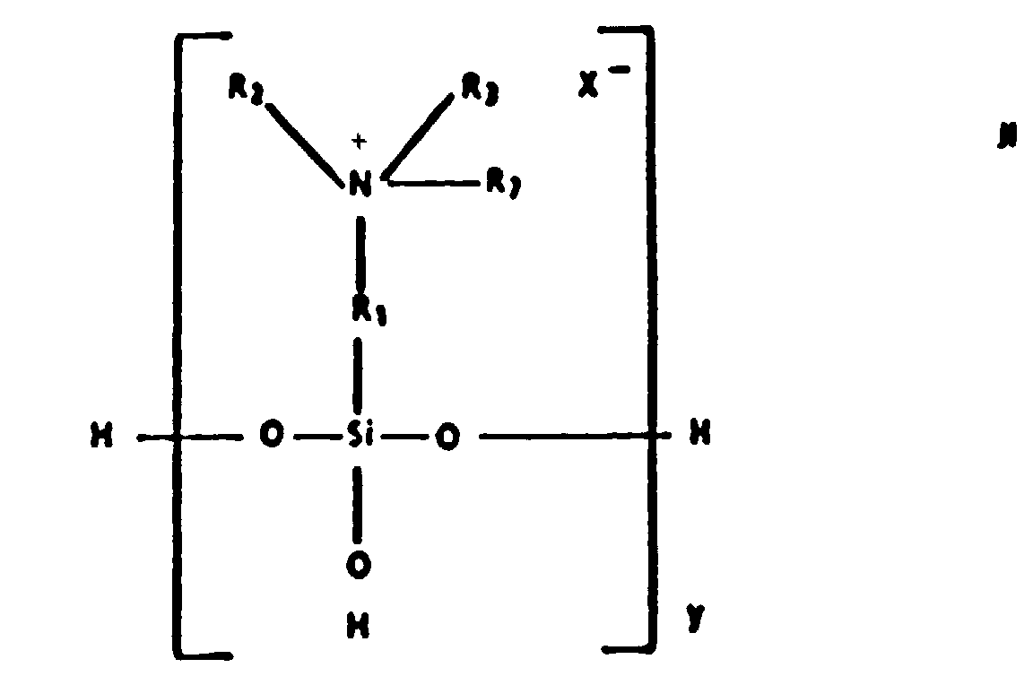
- The hydrolyzed silane may be prepared by hydrolyzing a silane having the following structural formula:
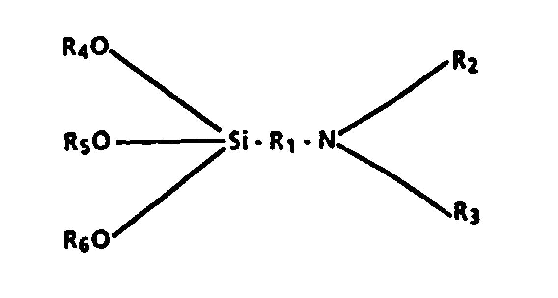
- If R1 is extended into a long chain, the compound becomes less stable. Silanes in which R1 contains about 3 to about 5 carbon atoms are preferred because the molecule is more stable, is more flexible and is under less strain. Optimum results are achieved when R1 contains 3 carbon atoms. Satisfactory results are achieved when R2 and R3 are alkyl groups. Optimum smooth and uniform films are formed with hydrolyzed silanes in which R2 and R3 are hydrogen. Satisfactory hydrolysis of the silane may be effected when R4, R5 and R6 are alkyl groups containing 1 to 4 carbon atoms. When the alkyl groups exceed 4 carbon atoms, hydrolysis becomes impractically slow. However, hydrolysis of silanes with alkyl groups containing 2 carbon atoms is preferred for best results.
- During hydrolysis of the amino silanes described above, the alkoxy groups are replaced with hydroxyl groups. As hydrolysis continues, the hydrolyzed silane takes on the following intermediate general structure:

- Chemical modification of the reactive amino, imino or tertiary amine groups above with metal ions by complexing or chelating eliminates the detrimental effects of the reactive group.
- The hydrolyzed silane solution may be prepared by adding sufficient water to hycrolyze the alkoxy groups attached to the silicon atom to form a solution. Insufficient water with normally cause the hydrolyzed silane to form an undesirable gel. Generally, dilute solutions are preferred for achieving thin coatings. Satisfactory reaction product films may be achieved with solutions containing from about 0.01 percent by weight to about 5 percent by weight of the silane. A solution containing from about 0.05 percent by weight to about 2 percent by weight silane based on the total weight of solution are preferred for stable solutions which form uniform reaction product layers.
- Solutions of metal salts, for example acetates, chlorides, bromides, iodides and other soluble species, may be used for the chelation of the reactive amino, imino or tertiary amine groups. Stoichiometric reactions with the nitrogen groups of the blocking material are preferred. for example, ethanol solutions of cupric acetate and 3-aminopropyl triethoxysilane may be prepared to give a 1:4 atom ratio of copper to nitrogen and a water content of about 10% to about 15%. Similarly, metal to nitrogen ratios of 1:2, 1:3, 1:4, 1:5, 1:6 and higher may be used depending on the coordination capacity of the metal and the stereochemistry of the resulting complex. Water content may range from about 5% to about 20%.
- Control of the pH of the hydrolyzed silane solution may be effected with any suitable organic or inorganic acid or acidic salt. Typical organic and inorganic acids and acidic salts include acetic acid, citric acid, formic acid, hydrogen iodide, phosphoric acid, ammonium chloride, hydrofluorsilicic acid, bromocresol green, bromophenol blue, p-toluene sulfonic acid and the like.
- Any suitable technique may be utilized to apply the blocking layer solution of the invention. Typical application techniques include spraying, dip coating, roll coating, wire wound roc coating, and the like. Hydrolyzed amino silanes complexed with metal described above are preferred.
- After drying, the siloxane reaction product film formed from the hydrolyzed silane contains larger molecules which may be linear, partially crosslinked, dimeric, trimeric, or otherwise oligomeric.
- Drying or curing of the hydrolyzed silane metal complex upon the conductive layer should be conducted at a temperature greater than about room temperature to provide a reaction product layer having more uniform electrical properties, more complete converssion of the hydrolyzed silane to siloxanes and less unreacted silanol. Generally, a reaction temperature between about 80°C and about 150°C is preferred for maximum stabilization of electrical chemical properties. The temperature selected depends to some extent on the specific conductive layer utilized and is limited by the temperature sensitivity of the substrate Reaction product layers having optimum electrical chemical stability are obtained when reactions are conducted at temperatures of about 120°C. The reaction temperature may be maintained by any suitable technique such as ovens, forced air ovens, radiant heat lamps, microwaves and the like.
- The reaction time depends upon the reaction temperatures used. Thus less reaction time is required when higher reaction temperatures are employed. Generally, increasing the reaction time increases the degree of cross-linking of the hydrolyzed silane. Satisfactory results have been achieved with reaction times between about 0.5 minute to about 45 minutes at elevated temperatures. For practical purposes, sufficient cross-linking is achieved by the time the reaction product layer is dry.
- The reaction may be conducted under any suitable pressure including atmospheric pressure or in a vacuum. Less heat energy is required when the reaction is conducted at subatmospheric pressures.
- One may readily determine whether sufficient condensation and cross-linking has occurred to form a siloxane reaction product film having stable electrical chemical properties in a machine environment by merely washing the siloxane reaction product film with water, toluene, tetrahydrofuran, methylene chloride or cyclohexanone and examining the washed siloxane reaction product film to compare infrared absorption of linear or cyclic Si-O- wavelength bands between about 1,000 to about 1,200 cm-1. It is believed that the partially polymerized reaction product contains siloxane and silanol moieties in the same molecule. The expression "partially polymerized" is used because total polymerization is normally not achievable even under the most severe drying or curing conditions.
- The blocking layers formed from the materials do not adversely interact with other layers of an electrophotographic imaging member, as the amino, imino or tertiary amine group is complexed with a metal. For example, the amine group of hydrolyzed gamma-aminopropyl triethoxysilane can be seen to be chelated to copper by the intense blue color of the resulting copper amine complex. Although the amine (or imino or tertiary amine group) is chelated, it is still available as a hole trap against injection. Further, the incorporation of metal such as copper allows for strong adhesion between a conductive layer of cuprous iodide and the blocking layer due to the interaction between the iodine of the copper iodide and the complexed copper. The stability of the blocking layer materials of the invention and the resistance to polymerization may be due to the chelation, and possibly due to zwitterion formation.
- A representative structure of an electrophotographic imaging member of the invention is shown in Figure 1. This imaging member is provided with a supporting substrate 1, an electrically
conductive ground plane 2, a charge blocking layer 3 comprising the charge blocking material of the invention, an optionaladhesive layer 4, acharge generating layer 5, and acharge transport layer 6. Other layers commonly used in electrophotographic imaging members may also be used, such as anti-curl layers, overcoating layers, and the like. - A description of the layers of the electrophotographic imaging member shown in Figure 1 follows.
- The supporting substrate may be opaque or substantially transparent and may comprise numerous suitable materials having the required mechanical properties. The substrate may further be provided with an electrically conductive surface. Accordingly, the substrate may comprise a layer of an electrically non-conductive or conductive material such as an inorganic or organic composition. As electrically non-conducting materials, there may be employed various resins known for this purpose including polyesters, polycarbonates, polyamides, polyimides, polyurethanes, and the like. The electrically insulating or conductive substrate can be flexible and may have any number of different configurations such as, for example, a sheet, a scroll, an endless flexible belt, and the like. Preferably, the substrate is in the form of an endless flexible belt and comprises a commercially available biaxially oriented polyester known as Mylar, available from E.I. du Pont de Nemours & Co., or Melinex, available from ICI Americas Inc., or Hostaphan, available from American Hoechst Corporation.
- The thickness of the substrate layer depends on numerous factors, including mechanical performance and economic considerations. The thickness of this layer may range from about 65 micrometers to about 150 micrometers, and preferably from about 75 micrometers to about 125 micrometers for optimum flexibility and minimum induced surface bending stress when cycled around small diameter rollers, e-g., 19 millimeter diameter rollers. The substrate for a flexible belt may be of substantial thickness, for example, over 200 micrometers, or of minimum thickness, for example less than 50 micrometers, provided there are no adverse effects on the final photoconductive device. The surface of the substrate layer is preferably cleaned prior to coating to promote greater adhesion of the deposited coating. Cleaning may be effected by exposing the surface of the substrate layer to plasma discharge, ion bombardment, solvent treatment and the like.
- The electrically conductive ground plane may be an electrically conductive metal layer which may be formed, for example, on the substrate by any suitable coating technique, such as a vacuum depositing technique. The conductive layer may comprise cuprous iodide. Cuprous iodide is particularly desirable for a highly transparent conductive layer. The properties of cuprous iodide are not adversely affected when the blocking layer materials of the invention are utilized. When cuprous iodide is used as the conductive layer, it is preferred that an adhesive layer be provided between the cuprous iodide conductive layer and the supporting substrate for improving adhesion.
- Other conductive materials such as metals may also be used for the conductive layer. Typical metals include aluminum, copper, gold, zirconium, niobium, tantalum, vanadium, hafnium, titanium, nickel, stainless steel, chromium, tungsten, molybdenum, and the like, and mixtures or alloys thereof.
- The conductive layer need not be limited to metals or cuprous iodide. For example, other I-VII semiconductors can be used such as cuprous bromide or chloride, or the corresponding silver salts. Other examples of conductive layers may be combinations of materials such as conductive indium tin oxide as a highly transparent layer for light having a wavelength between about 4000 Angstroms and about 9000 Angstroms or a conductive carbon black dispersed in a plastic binder as a semi-transparent or opaque conductive layer.
- The conductive layer may vary in thickness aver substantially wide ranges depending on the conductivity, optical transparency and flexibility desired for the electrophotoconductive member. Accordingly, for a flexible photoresponsive imaging device, the thickness of the conductive layer may be between about 50 Angstroms to about 1000 Angstroms, and more preferably from about 200 Angstroms to about 800 Angstroms for an optimum combination of electrical conductivity, flexibility and light transmission.
- After deposition of the electrically conductive ground plane layer, the blocking layer of the invention may be applied thereto as discussed above in detail. Electron blocking layers for positively charged photoreceptors allow holes from the imaging surface of the photoreceptor to migrate toward the conductive layer. For negatively charged photoreceptors, any suitable hole blocking layer of the invention capable of forming a barrier to prevent hole injection from the conductive layer to the opposite photoconductive layer may be utilized. The thickness of the blocking layer may range from about 20 Angstroms to about 4000 Angstroms, and preferably ranges from about 150 Angstroms to about 2000 Angstroms.
- In most cases, intermediate layers between the blocking layer and the adjacent charge generating or photogenerating layer may be desired to promote adhesion. For example, the
adhesive layer 4 may be employed. If such layers are utilized, they preferably have a dry thickness between about 0.001 micrometer to about 0.2 micrometer. Typical adhesive layers include film-forming polymers such as polyester, du Pont 49,000 resin (available from E.I. du Pont de Nemours & Co.), Vitel PE-100 and PE-200 (available from Goodyear Rubber & Tire Co.), polyvinylbutyral, polyvinylpyrrolidone, polyurethane, polymethyl methacrylate, phenoxy resin, and the like. - Du Pont 49,000 is a linear saturated copolyester of four diacids and ethylene glycol having a molecular weight of about 70,000 and a glass transition temperature of 32°C. Its molecular structure is represented as

- Vitel PE-100 is a linear copolyester of two diacids and ethylene glycol having a molecular weight of about 50,000 and a glass transition temperature of 71°C. Its molecular structure is represented as

- Vitel PE-200 is a linear saturated copolyester of two diacids and two diols having a molecular weight of about 45,000 and a glass transition temperature of 67°C. The molecular structure is represented as

- Any suitable charge generating (photogenerating) layer may be applied to the
adhesive layer 4. Examples of materials for photogenerating layers include inorganic photoconductive particles such as amorphous selenium, trigonal selenium, and selenium alloys selected from the group consisting of selenium-tellurium, selenium- tellurium-arsenic, selenium arsenide; and phthalocyanine pigment such as the X-form of metal-free phthalocyanine described in U.S. Patent No. 3,357,989, metal phthalocyanines such as vanadyl phthalocyanine and copper phthalocyanine; dibromoanthanthrone, squarylium, quinacridones such as those available from du Pont under the tradenames Monastral Red, Monastral Violet and Monastral Red Y; dibromo anthanthrone pigments such as those available under the trade names Vat orange 1 and Vat orange 3; benzimidazole perylene; substituted 2,4-diamino- triazines disclosed in U.S. Patent No. 3,442,781; polynuclear aromatic quinones such as those available from Allied Chemical Corporation under the tradenames Indofast Double Scarlet, Indofast Violet Lake B, Indofast Brilliant Scarlet and Indofast Orange; and the like, dispersed in a film forming polymeric binder. Multi- photogenerating layer compositions may be utilized where a photoconductive layer enhances or reduces the properties of the photogenerating layer. Examples of this type of configuration are described in U.S. Patent No 4,415,639. Other suitable photogenerating materials known in the art may also be utilized, if desired. Charge generating layers comprising a photoconductive material such as vanadyl phthalocyanine, metal-free phthalocyanine, benzimidazole perylene, amorphous selenium, trigonal selenium, selenium alloys such as selenium-tellurium, selenium-tellurium-arsenic, selenium arsenide, and the like and mixtures thereof are especially preferred because of their sensitivity to white light. Vanadyl phthalocyanine, metal-free phthalocyanine and tellurium alloys are also preferred because these materials provide the additional benefit of being sensitive to near infrared light. - Any suitable polymeric film-forming binder material may be employed as the matrix in the photogenerating layer. Typical polymeric film-forming materials include those described, for example, in U.S. Patent No. 3,121,006. The binder polymer should adhere well to the adhesive layer, dissolve in a solvent which also dissolves the upper surface of the adhesive layer and be miscible with the copolyester of the adhesive layer to form a polymer blend zone. Typical solvents include tetrahydrofuran, cyclohexanone, methylene chloride, 1,1,1-trichloroethane, 1, 1,2-trichloroethane, trichloroethylene, toluene, and the like, and mixtures thereof. Mixtures of solvents may be utilized to control evaporation range For example, satisfactory results may be achieved with a tetrahydrofuran to toluene ratio of between about 90:10 and about 10:90 by weight. Generally, the combination of photogenerating pigment, binder polymer and solvent should form uniform dispersions of the photogenerating pigment in the charge generating layer coating composition. Typical combinations include polyvinylcarbazole, trigonal selenium and tetrahydrofuran, phenoxy resin, trigonal selenium and toluene; and polycarbonate resin, vanadyl ohthalocyanine and methylene chloride. The solvent for the charge generating layer binder polymer should dissolve the polymer binder utilized in the charge-generating layer and be capable of dispersing the photogenerating pigment particles present in the charge generating layer.
- The photogenerating composition or pigment may be present in the resinous binder composition in various amounts. Generally, from about 5 percent by volume to about 90 percent by volume of the photogenerating pigment is dispersed in about 10 percent by volume to about 90 percent by volume of the resinous binder. Preferably from about 20 percent by volume to about 30 percent by volume of the photogenerating pigment is dispersed in about 70 percent by volume to about 80 percent by volume of the resinous binder composition. In one embodiment about 8 percent by volume of the photogenerating pigment is dispersed in about 92 percent by volume of the resinous binder composition.
- The photogenerating layer generally ranges in thickness from about 0.1 micrometer to about 5.0 micrometers, preferably from about 0.3 micrometer to about 3 micrometers. The photogenerating layer thickness is related to binder content. Higher binder content compositions generally require thicker layers for photogeneration. Thicknesses outside these ranges can be selected, providing the objectives of the present invention are achieved.
- Any suitable and conventional technique may be utilized to mix and thereafter apply the photogenerating layer coating mixture to the previously dried adhesive layer. Typical application techniques include spraying, dip coating, roll coating, wire wound rod coating, and the like. Drying of the deposited coating may be effected by any suitable conventional technique such as oven drying, infrared radiation drying, air drying and the like, to remove substantially all of the solvents utilized in applying the coating.
- The
charge transport layer 6 may comprise any suitable transparent organic polymer or non-polymeric material capable of supporting the injection of photo- generated holes or electrons from thecharge generating layer 5 and allowing the transport of these holes or electrons through the organic layer to selectively discharge the surface charge. The charge transport layer not only serves to transport holes or electrons, but also protects the photoconductive layer from abrasion or chemical attack, and therefore extends the operating life of the photoreceptor imaging member. The charge transport layer should exhibit negligible, if any, discharge when exposed to a wavelength of light useful in xerography, e.g. 4000 Angstroms to 9000 Angstroms. The charge transport layer is normally transparent in a wavelength region in which the photoconductor is to be used when exposure is effected therethrough is ensure that most of the incident radiation is utilized by the underlying charge generating layer. When used with a transparent substrate, imagewise exposure or erasure may be accomplished through the substrate with all light passing through the substrate. In this case, the charge transport material need not transmit light in the wavelength region of use. The charge transport layer in conjunction with the charge- generating layer is an insulator to the extent that an electrostatic charge placed on the charge transport layer is not conducted in the absence of illumination. - The charge transport layer may comprise activating compounds or charge transport molecules dispersed in normally electrically inactive film-forming polymeric materials for making these materials electrically active. These charge transport molecules may be added to polymeric materials which are incapable of supporting the injection of photogenerated holes and incapable of allowing the transport of these holes. An especially preferred transport layer employed in multilayer photoconductors comprises from about 25 percent to about 75 percent by weight of at least one charge-transporting aromatic amine, and about 75 percent to about 25 percent by weight of a polymeric film-forming resin in which the aromatic amine is soluble.
- The charge transport layer is preferably formed from a mixture comprising at least one aromatic amine compound of the formula:
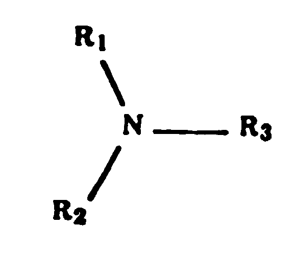
- I. Triphenyl amines such as:

- II. Bis and poly triarylamines such as:
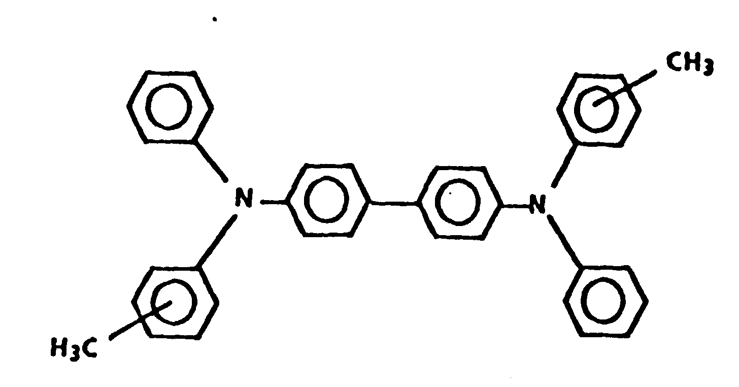
- III. Bis arylamine ethers such as:

- IV. Bis alkyl-arylamines such as:

- A preferred aromatic amine compound has the general formula:

- Examples of charge-transporting aromatic amines represented by the structural formulae above include triphenylmethane, bis(4-diethylamine-2-methylphenyl)phenylmethane, 4-4′-bis(diethylamino)-2,2′-dimethyltriphenylmethane; N,N′-bis(alkylphenyl)-(1,1′-biphenyl)-4,4′-diamine wherein the alkyl is, for example, methyl, ethyl, propyl, n-butyl, etc.; N,N′-diphenyl-N,N′-bis(3-methylphenyl)-(1,1′biphenyl)-4,4′-diamine; and the like, dispersed in an inactive resin binder.
- Any suitable inactive resin binder soluble in methylene chloride or other suitable solvents may be employed. Typical inactive resin binders soluble in methylene chloride include polycarbonate resin, polyvinylcarbazole, polyester, polyarylate, polyacrylate, polyether, polysulfone, and the like. Molecular weights can vary from about 20,000 to about 1,500,000. Other solvents that may dissolve these binders include tetrahydrofuran, tol uene, trichloroethylene, 1,1,2-trichloroethane, 1,1,1-trichloroethane, and the like.
- The preferred electrically inactive resin materials are polycarbonate resins having a molecular weight from about 20,000 to about 120,000, more preferably from about 50,000 to about 100,000. The materials most preferred as the electrically inactive resin material are poly(4,4′-dipropylidene-diphenylene carbonate) with a molecular weight of from about 35,000 to about 40,000, available as Lexan 145 from General Electric Company; poly(4,4′-isopropylidenediphenylene carbonate) with a molecular weight of from about 40,000 to about 45,000, available as Lexan 141 from General Electric Company; a polycarbonate resin having a molecular weight of from about 50,000 to about 100,000, available as Makrolon from Farbenfabricken Bayer A.G., a polycarbonate resin having a molecular weight of from about 20,000 to about 50,000, available as Merlon from Mobay Chemical Company; polyether carbonates; and 4,4′-cyclohexylidene diphenyl polycarbonate. Methylene chloride solvent is a desirable component of the charge transport layer coating mixture for adequate dissolving of all the components and for its low boiling point.
- An especially preferred multilayer photoconductor comprises a charge-generating layer comprising a binder layer of photoconductive material and a contiguous hole transport layer of a polycarbonate resin material having a molecular weight of from about 20,000 to about 120,000, having dispersed therein from about 25 to about 75 percent by weight of one or more compounds having the formula:

- The thickness of the charge transport layer may generally range from about 10 micrometers to about 50 micrometers, and preferably from about 20 micrometers to about 35 micrometers. Optimum thicknesses may range from about 23 micrometers to about 31 micrometers.
- The invention will further be illustrated with reference to the following, nonlimiting examples, it being understood that these examples are intended to be illustrative only, and that the invention is not intended to be limited to the materials, conditions, process parameters and the like recited herein.
- A solution of 1.2 weight percent of cuprous iodide (Cul) in n-butyronitrile is sprayed upon a blow- formed polyester sleeve supported by a rotating mandrel with an automatic spray gun (Binks No. 61). The thickness of this substrate is 0.1 mm (4 mils). After drying for 10 minutes at 100°C, the Cul layer is 400 Angstroms thick. This conductive sleeve is cut into three rectangular pieces measuring 9 inches x 11 inches.
- A charge generating layer is coated on a first piece of 22.9cm x 28cm (9 inches x 11 inches) sleeve. About 1.5 grams of a dispersion of 33 volume percent trigonal selenium having a particle size between about 0.05 micron to about 0.20 micron and about 67 volume percent of poly(hydroxyether) resin, Bakelite phenoxy PKHH available from Union Carbide Corporation is added to about 2.5 grams of a solution of tetrahydrofuran containing about 0.025 grams of N,N'-diphenyl-N,N'-bis(3-methylphenyl)1,1'-biphenyl-4,4'-diamine. This mixture is applied with a 0.00127cm (0.0005 inch) Bird applicator to the Cul layer and the device is then allowed to dry at 135°C for 3 minutes resulting in the formation of a hole generating layer having a dry thickness of about 0.6 micron containing about 28 volume percent of trigonal selenium dispersed in about 72 volume percent of poly(hydroxyether). The generating layer is then overcoated with a 25 micron thick charge transport layer containing about 50 percent by weight N,N'-diphenyl- N,N'-bis(3-methylphenyl)1,1'-biphenyl-4,4'-diamine dispersed in about 50 percent by weight of polycarbonate resin, Makrolon, available from Bayer Corporation.
- The resulting photosensitive member having two electrically operative layers is subjected to electrical negative charging in a xerographic scanner. The results of the scanning test show only an approximately initial 150 volts charge acceptance. This suggests a strong injection of positive charges from the conductive Cul into the electrically active layers.
- A second device is fabricated using the same procedures as in Example I upon a second piece of cuprous iodide coated polyester with the exception that a blocking layer is coated between the Cul layer and the charge generating layer.
- An aqueous 10% water solution is prepared containing about 0.88 percent by weight based on the total weight of the solution (0.004 mole solution), of 3-aminopropyl triethoxysilane. The solution also contains about 95 percent by weight denatured ethanol and about 5 percent by weight isopropanol based on the total weight of the solution (0.004 mole solution). This solution is applied with a 0.00127cm (0.0005 inch) Bird applicator onto the surface of the Cul coated polyester film and thereafter dried at a temperature of about 135°C in a forced air oven for about 3 minutes to form a reaction product layer of the partially polymerized silane upon the Cul coated polyester film to form a dried layer having a thickness of about 450 Angstroms measured by infrared reflectance spectrometry and by ellipsometry.
- The resulting photosensitive member having two electrically operative layers is subjected to electrical negative charging in a xerographic scanner. The results of scanning show that the device accepts a charge of more than 1000 volts and does not discharge under strong light exposure. This suggests that the silane blocking layer reacts with the Cul layer and destroys its conductivity.
- A third device is fabricated as in Comparative Example II upon the third piece of Cul coated polyester with the exception that a blocking layer of the invention is coated between the conductive cuprous iodide layer and the charge generating layer. 1.76g (0.008 mol) of 3- aminopropyl triethoxysilane is hydrolyzed in 8.24g of distilled water and 0.002 mol (0.36g) of anhydrous copper (II) acetate (Aldrich) is dissolved with gentle heating into 86.4g of 200 proof ethanol. After complete dissolution, this solution is added to the aqueous silane slowly under good stirring. A deep blue color develops. This solution is applied with a 0.00127cm (0.0005 inch) Bird coater on the surface of the Cul coated polyester film and thereafter dried at a temperature of about 135°C in a forced air oven for about 3 minutes to form a reaction product layer of the partially polymerized copper (II) modified silane. The layer has a dry thickness of about 1000 Angstroms. The resulting photosensitive device having two electrically operative layers is subjected to electrical cycling in a continuous rotating scanner and shows excellent xerographic properties.
- A blocking layer material is prepared from an ethanol solution of cupric acetate and gamma-amino-propyl triethoxysilane, giving a 1:4 ratio of copper to amine and a water content of 10 to 15% using the same procedures as described in Example III.
- A full electrophotographic device is fabricated with the blocking material. In particular, a photoconductive imaging member is prepared by providing a web of Cul (0.06 micron thickness) coated polyester (Melinex) substrate having a thickness of 0.0762mm (3 mils), and applying thereto, using a gravure applicator, a solution containing about 2.1 weight percent of the charge blocking layer solution. This layer is then dried for 10 minutes atl 35°C in a forced air oven. The resulting blocking layer has a dry thickness of about 0.1 micrometer.
- An adhesive interface layer is then prepared by applying a wet coating containing 49,000 polyester (du Pont) over the blocking layer, using a gravure applicator. The adhesive interface layer is then dried for 10 minutes at 135°C in a forced air oven. The resulting adhesive interface layer has a dry thickness of 0.05 micrometer.
- The adhesive interface layer is thereafter coated with a photogenerating layer containing 7.5 percent by volume trigonal selenium, 25 percent by volume N,N'-diphenyl-N,N'-bis(3-methyl-phenyl)-1,1'-biphenyl-4,4'-diamine, and 67.5 percent by volume polyvinylcarbazole. This photogenerating layer is prepared by introducing 80 grams polyvinylcarbazole to 1400 ml of a 1:1 volume ratio of a mixture of tetrahydrofuran and toluene. To this solution are added 80 grams of trigonal selenium and 10,000 grams of 0.32cm (1/8 inch) diameter stainless steel shot. mixture is then placed on a ball mill for 72 to 96 hours. Subsequently, 500 grams of the resulting slurry are added to a solution of 36 grams of polyvinylcarbazole and 20 grams of N,N'-diphenyl-N,N'- bis(3-methylphenyl)-1,1'-biphenyl-4,4'-diamine in 750 ml of 1:1 volume ratio of tetrahydrofuran/toluene. This slurry is then placed on a shaker for 10 minutes. The resulting slurry is thereafter applied to the adhesive interface with an extrusion die. This photogenerating layer is dried at 135°C for 5 minutes in a forced air oven to form a photogenerating layer having a dry thickness of 2.3 micrometers.
- This member is then coated over with a charge transport layer. The charge transport coating solution is prepared by introducing into a carboy container in a weight ratio of 1:1 N,N'-diphenyl-N,N'-bis(3-methylphenyl)-1,1'-biphenyl-4,4'-diamine, and the binder resin Makrolon 5705, a polycarbonate having a weight average molecular weight from about 50,000 to about 1,000,000, available from Farbenfabricken Bayer AG. The resulting solid mixture is dissolved in methylene chloride to provide a 15 weight percent solution thereof. This solution is then applied onto the photogenerator layer by extrusion coating to form a wet charge transport layer. The resulting photoconductive member is then dried at 135°C in a forced air oven for 5 minutes to produce a 25 micrometers dry thickness charge transport layer.
- The resulting photosensitive device having two electrically operative layers is subjected to electrical testing in a continuous rotating scanner and shows excellent xerographic properties.
- The same procedures are followed as described in Comparative Example I except that a blocking solution of silane (0.004 mol) modified by cupric acetate (0 001 mol) in a 85:15 ratio of alcohol (95% ethanol and 5% isopropyl aicohol):water is sprayed with an automatic spray gun (Binks No. 61) upon the electrically conductive cuprous iodide coated sleeve. This sleeve is supported by a rotating mandrel. After spraying, the sleeve is dried at 100°C for 10 minutes. A charge generating layer is applied from a solution of vanadyl phthalocyanine (80 percent by volume) in Vitel PE-100 polyester (Goodyear) (20 percent by volume) by spraying with an automatic spray gun (Binks No. 61) upon the blocking layer coated sleeve supported by a rotating mandrel. The sprayed layer is dried for one hour at 100°C and has a dry layer thickness of 0.6 micron. Then a charge transport layer of 40 percent by weight N-N'-diphenyl-N,N'-bis(3-methylphenyl) 1,1′biphenyl diamine in 60 percent by weight bisphenol A-polycarbonate Merlon (Mobay) is sprayed from a solution of 80 parts methylene chloride and 20 parts 1,1,2-trichloroethane with an automatic spray gun (Binks No. 61) in a climatized spray room (18°C/5% RH). After spraying, the device is dried in a forced air oven at 80°C for 10 minutes, at 100°C for 10 minutes, and at 120°C for 10 minutes. The thickness of this layer is 19 microns.
- This photoreceptor is evaluated in a rotating xerographic scanner for 50,000 cycles. The scanning results show excellent xerographic properties.
- The same procedures as described in Example III are followed except that the substrate polyester film (Mylar from du Pont) is vacuum coated with 120 Angstroms thickness of titanium in place of the conductive cuprous iodide layer. The resulting photoreceptor exhibits excellent xerographic properties.
- The same procedures are followed as in Example V except that a blocking layer of 0.006 mol 3-aminopropyl triethoxysilane and 0.001 mol cobalt II acetate is used. The electrical cycling results are the same as those for the photoreceptor of Example V.
- The same procedures are followed as in Example VI except that the blocking layer is made of 0.002 mol 3- aminopropyl triethoxysilane, 0.002 mol 3-aminopropyl triethoxysilane acetate, and 0.001 mol zinc acetate. The electrical cycling results are very similar to those of Example VI.
- While the invention has been described with reference to specific preferred embodiments, it is not intended to be limited thereto. Rather, those skilled in the art will recognize that variations and modifications may be made therein which are within the scope of the claims.
Claims (13)
- A composition comprised of a complex of a film forming charge blocking polymer containing at least one nitrogen-containing group, said polymer being other than an 8-hydroxy quinoline, a dipyridylamine or a cross-linked polyethylene imine, the at least one nitrogen-containing group being chelated to a metal ion or atom.
- A composition as claimed in claim 1, characterised in that said nitrogen-containing group is selected from the group consisting of amino, imino and tertiary amine.
- A composition as claimed in claim 1 or claim 2, characterised in that said metal ion or atom is a transition metal or is at least one member selected from the group consisting of copper, silver, gold, nickel, palladium, platinum, cobalt, rhodium, irridium, iron, ruthenium, osmium, manganese, chromium, vanadium, titanium, zinc, cadmium, mercury and lead.
- A composition as claimed in any one of claims 1 to 3, characterised in that said film forming charge blocking polymer is a silane.
- A composition as claimed in any one of claims 1 to 4, chacterised in that said complex or salt is a 3-aminopropyl triethoxysilane metal complex or is 3-aminopropyl triethoxysilane complexed with copper.
- An electrophotographic imaging member, comprising a charge blocking layer (3) comprised of a metal complex or salt of a film forming polymer containing at least one nitrogen-containing group, the at least one nitrogen-containing group being chelated to a metal ion or atom.
- An imaging member as claimed in claim 6, characterised in that said nitrogen-containing group is selected from the group consisting of amino, imino and tertiary amine.
- An imaging member as claimed in claim 6 or claim 7, characterised in that said metal ion or atom is a transition metal or is at least one member selected from the group consisting of copper, silver, gold, nickel, palladium, platinum, cobalt, rhodium, iridium, iron, ruthenium, osmium, manganese, chromium, vanadium, titanium, zinc, cadmium, mercury and lead.
- An imaging member as claimed in any one of claims 6 to 8, characterised in that said film forming charge blocking polymer is a silane.
- An imaging member as claimed in any one of claims 6 to 9, characterised in that said complex or salt is a 3-aminopropyl triethoxysilane metal complex or is 3-aminopropyl triethoxysilane complexed with copper.
- An imaging member as claimed in any one of claims 6 to 10, further including a conductive layer (2) comprising cuprous iodide adjacent said charge blocking layer (3).
- An electrophotographic imaging member as claimed in any one of claims 6 to 11, including a supporting substrate (1), a conductive layer (2), said charge blocking layer (3), an adhesive layer (4), a charge generating layer (5) and a charge transport layer (6).
- An imaging member as claimed in claim 12, characterised in that said conductive layer (2) comprises cuprous iodide.
Applications Claiming Priority (2)
| Application Number | Priority Date | Filing Date | Title |
|---|---|---|---|
| US575610 | 1984-01-31 | ||
| US07/575,610 US5091278A (en) | 1990-08-31 | 1990-08-31 | Blocking layer for photoreceptors |
Publications (2)
| Publication Number | Publication Date |
|---|---|
| EP0473448A1 EP0473448A1 (en) | 1992-03-04 |
| EP0473448B1 true EP0473448B1 (en) | 1996-12-04 |
Family
ID=24301005
Family Applications (1)
| Application Number | Title | Priority Date | Filing Date |
|---|---|---|---|
| EP91307955A Expired - Lifetime EP0473448B1 (en) | 1990-08-31 | 1991-08-30 | Electrophotographic imaging member |
Country Status (4)
| Country | Link |
|---|---|
| US (1) | US5091278A (en) |
| EP (1) | EP0473448B1 (en) |
| JP (1) | JP3292304B2 (en) |
| DE (1) | DE69123404T2 (en) |
Families Citing this family (15)
| Publication number | Priority date | Publication date | Assignee | Title |
|---|---|---|---|---|
| JPH0519516A (en) * | 1991-07-10 | 1993-01-29 | Fuji Xerox Co Ltd | Electrophotographic sensitive body |
| US5415961A (en) * | 1992-09-29 | 1995-05-16 | Xerox Corporation | Flexible belt supported on rigid drum for electrophotographic imaging |
| US5550618A (en) * | 1993-05-18 | 1996-08-27 | Xerox Corporation | Drum imaging structure with photosensitive member |
| US5413810A (en) * | 1994-01-03 | 1995-05-09 | Xerox Corporation | Fabricating electrostatographic imaging members |
| US5562840A (en) * | 1995-01-23 | 1996-10-08 | Xerox Corporation | Substrate reclaim method |
| JPH08220790A (en) * | 1995-02-14 | 1996-08-30 | Fuji Xerox Co Ltd | Electrophotographic photoreceptor |
| US5529870A (en) * | 1995-05-11 | 1996-06-25 | Xerox Corporation | Halogenindium phthalocyanine crystals |
| US5876887A (en) * | 1997-02-26 | 1999-03-02 | Xerox Corporation | Charge generation layers comprising pigment mixtures |
| SE0000090D0 (en) * | 2000-01-13 | 2000-01-13 | Astrazeneca Ab | Method and apparatus for monitoring |
| US7279050B2 (en) | 2002-10-29 | 2007-10-09 | Xerox Corporation | One-piece bottom edge wipe sponge for cleaning a photoreceptor drum |
| US7947417B2 (en) * | 2004-11-18 | 2011-05-24 | Xerox Corporation | Processes for the preparation of high sensitivity titanium phthalocyanines photogenerating pigments |
| US7824830B2 (en) * | 2004-12-20 | 2010-11-02 | Ricoh Company Limited | Coating liquid and electrophotographic photoreceptor prepared using the coating liquid |
| JP5473542B2 (en) * | 2009-11-04 | 2014-04-16 | キヤノン株式会社 | Method for producing electrophotographic photosensitive member |
| US8481655B2 (en) * | 2011-07-27 | 2013-07-09 | Wacker Chemical Corporation | Copper complexes of amino-functional organosilicon compounds and their use |
| CN114512615A (en) * | 2021-12-29 | 2022-05-17 | 电子科技大学 | Organic photoelectric detector based on organic-metal ion chelated electron transport layer |
Family Cites Families (21)
| Publication number | Priority date | Publication date | Assignee | Title |
|---|---|---|---|---|
| US3121006A (en) * | 1957-06-26 | 1964-02-11 | Xerox Corp | Photo-active member for xerography |
| US3357989A (en) * | 1965-10-29 | 1967-12-12 | Xerox Corp | Metal free phthalocyanine in the new x-form |
| US3442781A (en) * | 1966-01-06 | 1969-05-06 | Xerox Corp | Photoelectrophoretic and xerographic imaging processes employing triphenodioxazines as the electrically photosensitive component |
| US4265990A (en) * | 1977-05-04 | 1981-05-05 | Xerox Corporation | Imaging system with a diamine charge transport material in a polycarbonate resin |
| US4291110A (en) * | 1979-06-11 | 1981-09-22 | Xerox Corporation | Siloxane hole trapping layer for overcoated photoreceptors |
| US4286033A (en) * | 1980-03-05 | 1981-08-25 | Xerox Corporation | Trapping layer overcoated inorganic photoresponsive device |
| US4338387A (en) * | 1981-03-02 | 1982-07-06 | Xerox Corporation | Overcoated photoreceptor containing inorganic electron trapping and hole trapping layers |
| GB2097414A (en) * | 1981-04-01 | 1982-11-03 | Fulmer Res Inst Ltd | Protection of metal surfaces |
| US4415639A (en) * | 1982-09-07 | 1983-11-15 | Xerox Corporation | Multilayered photoresponsive device for electrophotography |
| US4464450A (en) * | 1982-09-21 | 1984-08-07 | Xerox Corporation | Multi-layer photoreceptor containing siloxane on a metal oxide layer |
| JPS59223440A (en) * | 1983-06-03 | 1984-12-15 | Fuji Xerox Co Ltd | Electrophotographic sensitive body |
| US4725518A (en) * | 1984-05-15 | 1988-02-16 | Xerox Corporation | Electrophotographic imaging system comprising charge transporting aromatic amine compound and protonic acid or Lewis acid |
| US4599286A (en) * | 1984-12-24 | 1986-07-08 | Xerox Corporation | Photoconductive imaging member with stabilizer in charge transfer layer |
| JPS61203131A (en) * | 1985-03-04 | 1986-09-09 | Agency Of Ind Science & Technol | Novel chelate resin and its production |
| US4639402A (en) * | 1985-08-02 | 1987-01-27 | Xerox Corporation | Photoreceptor containing selenium particles coated with a reaction product of a hydrolyzed silane |
| US4654284A (en) * | 1985-10-24 | 1987-03-31 | Xerox Corporation | Electrostatographic imaging member with anti-curl layer comprising a reaction product of a binder bi-functional coupling agent and crystalline particles |
| US4664995A (en) * | 1985-10-24 | 1987-05-12 | Xerox Corporation | Electrostatographic imaging members |
| JPS63199363A (en) * | 1987-02-16 | 1988-08-17 | Ricoh Co Ltd | electrophotographic photoreceptor |
| US4780385A (en) * | 1987-04-21 | 1988-10-25 | Xerox Corporation | Electrophotographic imaging member containing zirconium in base layer |
| US4786570A (en) * | 1987-04-21 | 1988-11-22 | Xerox Corporation | Layered, flexible electrophotographic imaging member having hole blocking and adhesive layers |
| US4806443A (en) * | 1987-06-10 | 1989-02-21 | Xerox Corporation | Polyarylamine compounds and systems utilizing polyarylamine compounds |
-
1990
- 1990-08-31 US US07/575,610 patent/US5091278A/en not_active Expired - Fee Related
-
1991
- 1991-08-22 JP JP21107191A patent/JP3292304B2/en not_active Expired - Fee Related
- 1991-08-30 DE DE69123404T patent/DE69123404T2/en not_active Expired - Fee Related
- 1991-08-30 EP EP91307955A patent/EP0473448B1/en not_active Expired - Lifetime
Also Published As
| Publication number | Publication date |
|---|---|
| EP0473448A1 (en) | 1992-03-04 |
| JP3292304B2 (en) | 2002-06-17 |
| DE69123404T2 (en) | 1997-06-12 |
| JPH04270773A (en) | 1992-09-28 |
| US5091278A (en) | 1992-02-25 |
| DE69123404D1 (en) | 1997-01-16 |
Similar Documents
| Publication | Publication Date | Title |
|---|---|---|
| US6194111B1 (en) | Crosslinkable binder for charge transport layer of a photoconductor | |
| US4786570A (en) | Layered, flexible electrophotographic imaging member having hole blocking and adhesive layers | |
| US6933089B2 (en) | Imaging member | |
| EP0289216B1 (en) | Electrophotographic imaging member | |
| US5830614A (en) | Multilayer organic photoreceptor employing a dual layer of charge transporting polymers | |
| US5008167A (en) | Internal metal oxide filled materials for electrophotographic devices | |
| US5055366A (en) | Polymeric protective overcoatings contain hole transport material for electrophotographic imaging members | |
| EP0473448B1 (en) | Electrophotographic imaging member | |
| CA2164033C (en) | Multilayered photoreceptor | |
| US5576130A (en) | Photoreceptor which resists charge deficient spots | |
| US5571649A (en) | Electrophotographic imaging member with improved underlayer | |
| US5422213A (en) | Multilayer electrophotographic imaging member having cross-linked adhesive layer | |
| US5149609A (en) | Polymers for photoreceptor overcoating for use as protective layer against liquid xerographic ink interaction | |
| US5571647A (en) | Electrophotographic imaging member with improved charge generation layer | |
| US5418100A (en) | Crack-free electrophotographic imaging device and method of making same | |
| US5283143A (en) | Electrophotographic imaging member containing arylamine terpolymers with CF3 substituted moieties | |
| US5643702A (en) | Multilayered electrophotograpic imaging member with vapor deposited generator layer and improved adhesive layer | |
| US5686215A (en) | Multilayered electrophotographic imaging member | |
| US5166381A (en) | Blocking layer for photoreceptors | |
| US7704656B2 (en) | Photoconductive imaging member | |
| US7267917B2 (en) | Photoreceptor charge transport layer composition | |
| US5607802A (en) | Multilayered photoreceptor with dual underlayers for improved adhesion and reduced micro-defects | |
| EP0798346A2 (en) | Hydroxygallium phthalocyanine and alkoxygallium phthalocyanine dimers | |
| US5110700A (en) | Electrophotographic imaging member | |
| US5223361A (en) | Multilayer electrophotographic imaging member comprising a charge generation layer with a copolyester adhesive dopant |
Legal Events
| Date | Code | Title | Description |
|---|---|---|---|
| PUAI | Public reference made under article 153(3) epc to a published international application that has entered the european phase |
Free format text: ORIGINAL CODE: 0009012 |
|
| AK | Designated contracting states |
Kind code of ref document: A1 Designated state(s): DE FR GB |
|
| 17P | Request for examination filed |
Effective date: 19920904 |
|
| 17Q | First examination report despatched |
Effective date: 19950708 |
|
| GRAG | Despatch of communication of intention to grant |
Free format text: ORIGINAL CODE: EPIDOS AGRA |
|
| GRAG | Despatch of communication of intention to grant |
Free format text: ORIGINAL CODE: EPIDOS AGRA |
|
| GRAH | Despatch of communication of intention to grant a patent |
Free format text: ORIGINAL CODE: EPIDOS IGRA |
|
| GRAH | Despatch of communication of intention to grant a patent |
Free format text: ORIGINAL CODE: EPIDOS IGRA |
|
| GRAA | (expected) grant |
Free format text: ORIGINAL CODE: 0009210 |
|
| AK | Designated contracting states |
Kind code of ref document: B1 Designated state(s): DE FR GB |
|
| REF | Corresponds to: |
Ref document number: 69123404 Country of ref document: DE Date of ref document: 19970116 |
|
| ET | Fr: translation filed | ||
| PLBE | No opposition filed within time limit |
Free format text: ORIGINAL CODE: 0009261 |
|
| STAA | Information on the status of an ep patent application or granted ep patent |
Free format text: STATUS: NO OPPOSITION FILED WITHIN TIME LIMIT |
|
| 26N | No opposition filed | ||
| REG | Reference to a national code |
Ref country code: GB Ref legal event code: IF02 |
|
| PGFP | Annual fee paid to national office [announced via postgrant information from national office to epo] |
Ref country code: FR Payment date: 20020808 Year of fee payment: 12 |
|
| PGFP | Annual fee paid to national office [announced via postgrant information from national office to epo] |
Ref country code: GB Payment date: 20020828 Year of fee payment: 12 |
|
| PGFP | Annual fee paid to national office [announced via postgrant information from national office to epo] |
Ref country code: DE Payment date: 20020904 Year of fee payment: 12 |
|
| PG25 | Lapsed in a contracting state [announced via postgrant information from national office to epo] |
Ref country code: GB Free format text: LAPSE BECAUSE OF NON-PAYMENT OF DUE FEES Effective date: 20030830 |
|
| PG25 | Lapsed in a contracting state [announced via postgrant information from national office to epo] |
Ref country code: DE Free format text: LAPSE BECAUSE OF NON-PAYMENT OF DUE FEES Effective date: 20040302 |
|
| GBPC | Gb: european patent ceased through non-payment of renewal fee | ||
| PG25 | Lapsed in a contracting state [announced via postgrant information from national office to epo] |
Ref country code: FR Free format text: LAPSE BECAUSE OF NON-PAYMENT OF DUE FEES Effective date: 20040430 |
|
| REG | Reference to a national code |
Ref country code: FR Ref legal event code: ST |