EP0245745B1 - Image processing system - Google Patents
Image processing system Download PDFInfo
- Publication number
- EP0245745B1 EP0245745B1 EP87106443A EP87106443A EP0245745B1 EP 0245745 B1 EP0245745 B1 EP 0245745B1 EP 87106443 A EP87106443 A EP 87106443A EP 87106443 A EP87106443 A EP 87106443A EP 0245745 B1 EP0245745 B1 EP 0245745B1
- Authority
- EP
- European Patent Office
- Prior art keywords
- field
- signal
- sub
- memory
- video signals
- Prior art date
- Legal status (The legal status is an assumption and is not a legal conclusion. Google has not performed a legal analysis and makes no representation as to the accuracy of the status listed.)
- Expired - Lifetime
Links
- 230000015654 memory Effects 0.000 claims description 59
- 230000002441 reversible effect Effects 0.000 claims description 12
- 230000004044 response Effects 0.000 claims description 7
- 238000001514 detection method Methods 0.000 claims 2
- 238000010586 diagram Methods 0.000 description 13
- 238000005070 sampling Methods 0.000 description 5
- 239000002131 composite material Substances 0.000 description 1
- 230000010485 coping Effects 0.000 description 1
- 239000000284 extract Substances 0.000 description 1
- 230000006870 function Effects 0.000 description 1
- 230000036039 immunity Effects 0.000 description 1
- 238000012544 monitoring process Methods 0.000 description 1
- 230000001681 protective effect Effects 0.000 description 1
- 238000000926 separation method Methods 0.000 description 1
- 230000001131 transforming effect Effects 0.000 description 1
Images


Classifications
-
- H—ELECTRICITY
- H04—ELECTRIC COMMUNICATION TECHNIQUE
- H04N—PICTORIAL COMMUNICATION, e.g. TELEVISION
- H04N5/00—Details of television systems
- H04N5/44—Receiver circuitry for the reception of television signals according to analogue transmission standards
- H04N5/445—Receiver circuitry for the reception of television signals according to analogue transmission standards for displaying additional information
- H04N5/45—Picture in picture, e.g. displaying simultaneously another television channel in a region of the screen
Definitions
- the present invention relates to an image processing system.
- the image processing system of the present invention is especially suitable for use in an apparatus which receives two different video signals (for example, video signals from a magnetic recording/reproducing apparatus such as a video tape recorder and from a signal source such as a television tuner) compresses one of the two video signals on the time axis, merges the compressed video signal into the other video signal, and supplies the resultant signal to a Braun tube in a television set so that two-field images are displayed simultaneously on the Braun tube.
- two different video signals for example, video signals from a magnetic recording/reproducing apparatus such as a video tape recorder and from a signal source such as a television tuner
- a conventional apparatus using the above-described system is provided with two memories for storing one of the two different video signals to be displayed in a sub-field (small area) of the Braun tube.
- the sub-field is stored in a one-field memory and buffered in an additional buffer memory (EP 175 590).
- a multiplexer feeds the luminance signal Y and the color difference signals R-Y and B-Y alternatively to an A/D converter (IEEE Transactions on Consumer Electronics, vol. CE-25, Feb/1979, pages 152-158; M. Masuda et al.: "Fully digitalized color picture in picture television system").
- the video signal is sequentially written into the memories and at the same time the signal is read out from the memories in a compressed form.
- the retrieved signal is merged into the other video signal to be displayed in a main-field (large area) on the Braun tube.
- Writing and reading of the two memories are switched at the input and output stages of the memories in synchronism with the two video signals. Namely, writing into the memories is in synchronism with the sub-field video signal, while reading from the memories is in synchronism with the main-field video signal.
- An object of the present invention is to provide an image processing system which is simple in structure and is capable of satisfactory sub-field display.
- discriminating means for discriminating odd/even fields of each main-field and sub-field picture memory means for storing information of the sub-field picture, and address control means for controlling read/write timing of the sub-field picture information are employed.
- the sub-field coincides with the result of the field discrimination of the main-field picture to/from the memory means at an appropriate timing.
- a high resolution picture is realized compared to systems having only one field picture information, and no jolt in the vertical direction appears since the memory means includes both odd/even information, and the memory address control means supplies information which coincides with the result of the discrimination of the main-fields picture.
- a joint of two field appearing in the sub-field picture results in that rewriting new information during reading is prevented since the memory address control means controls so that the reading phase is always proceeding in a memory area corresponding to one field.
- Fig. 1 shows in block diagram the image processing system representing one embodiment of this invention.
- This embodiment is capable of accomplishing "picture-in-picture" for the sub-field with high picture equality using only one memory.
- the disturbance in sub-field which is caused by the outrun of the memory read phase over the memory write phase i.e., the misalignment of sub-field video signals (2-field display) read out of the memory, can be prevented.
- the embodiment will be described in detail with reference to the drawing.
- Shown by 301 and 302 are sync separation circuits connected to the first and second video signal sources for separating the vertical and horizontal sync signals from the video signal, 303 and 304 are field discriminating circuits for discriminating the field of the main-field video signal by receiving the sync signals, 305 is a false operation preventing circuit, 3' and 4' are switches operated in unison and connected to the outputs of the field discriminating circuits 303 and 304; 306 is a field information read/write outrun inhibit circuit which receives the sigal passing the switches and produces a control signal for controlling the switching control circuit 5 and a control signal for controlling the dual-port memory 12 in the time-axis compressing circuit in the video signal processing unit 220, and a television receiver set 16.
- the video signals including the main-field video signal and sub-field video signal originating from the video signal sources 1 and 2 are fed to the sync separating circuits 301 and 302, respectively, by which the vertical sync signal and horizontal sync signal are separated.
- the video signals are further fed through the field discriminating circuits 303 and 304 and switches 3' and 4', and supplied to the outrun inhibit circuit 306.
- the main-field video signal from the video signal source 2 is fed through the switch 3 to one input terminal of an adder 26.
- the sub-field video signal from the video signal source 1 is fed through the switch 4 to the memory 12, and after it is compressed on the time-axis by the memory it is delivered to another input terminal of the adder 26.
- the main and sub-field video signals merged by the adder 26 are delivered to the television receiver set 16, on which two fields are displayed to accomplish the "picture-in-picture" function.
- the false operation preventing circuit 305 and switching control circuit 5 play a protective role for coping with the field discrimination for the sync signals disturbed by noises and the transitional operation at exchange of two fields, and these circuits may be simplified or eliminated in some cases.
- FIGs. 2 and 3 are block diagrams for explaining the read/write operations of the memory 12. Shown in Fig. 2 by 10a is an analog-to-digital (A/D) converter, 10b is a sampling circuit, 10c is an automatic phase controller, 10d is a clock signal generator, 11a and 15a are switches, 60a-60d are areas of a memory 12, and 19 is a digital-to-analog (D/A) converter.
- A/D analog-to-digital
- 10b is a sampling circuit
- 10c is an automatic phase controller
- 10d is a clock signal generator
- 11a and 15a are switches
- 60a-60d are areas of a memory 12
- 19 is a digital-to-analog (D/A) converter.
- the sub-field video signal S1 in a digital form at the end of the A/D converter 10a is sampled by the sampling circuit 10b in response to the clock signal provided by the clock signal generator 10d.
- the clock signal is controlled by the automatic phase controller 10c to be in-phase with the burst signal of the sub-field video signal S1, and it has a frequency twice or more of the burst signal.
- the sampled signal is written into any of the areas 60a-60d in the memory 12.
- the memory readout operation takes place in asynchronous manner with the write operation.
- the memory read and write operations are carried out by switching the switches 11a and 15a by the control signal C (C1 and C2) from the outrun inhibit circuit 306 based on the result of field discrimination by the field discriminating circuits 303 and 304. Transforming the signal read out of the memory areas 60a-60d into an analog signal by the D/A converter 19 results in a signal S1' which is a time-axis compressed version of the sub-field video signal S1.
- a luminance signal extractor Shown in Fig. 3 by 6 is a luminance signal extractor, 8 is a color-difference separator, 8' is an automatic phase synchronization control circuit, 9 and 19d are switches, 10e is a color-difference and luminance switching circuit, 19a and 19b are D/A converters, and 19c is an adder.
- the difference between Fig. 2 and Fig. 3 is whether or not the sub-field video signal S1 is decomposed into the luminance signal and color-difference signal.
- the former can be called “composite system", and the latter "component system".
- the automatic phase synchronization control circuit 42 is used for the control.
- the circuit is known in the art and its detailed explanation will be omitted.
- the color signal separator 8 is merely required to demodulate the color-difference signal from the NTSC signal, and a commonly used demodulator suffices for this purpose.
- the luminance signal is extracted by the luminance signal extractor 6, and also in this case a usual low-pass filter suffices for the purpose.
- the input signal which has been decomposed into the luminance signal and color-difference signal is fed through the switch 9 to the A/D converter 10a, by which it is transformed into digital data in a time slicing manner. After that the data is stored in the memory areas 60a-60d by way of the sampling circuit 10b and switch 11a.
- This management of the signal is due to the use of a single A/D converter, and in exchange for the provision of a plurality of A/D converters the switch circuits 9 and 19d and the color-difference and luminance switching circuit 10e can be eliminated.
- the switch 19d In synchronism with the clock signal produced by the clock signal generator 10d, the switch 19d is operated by the signal C4 and at the same time sampling is implemented by the sampling circuit 10b. Accordingly, when the switch 19d is positioned to a-terminal, the luminance signal is A/D converted and sampled by the samping circuit 10b and then written in the memory areas 60a-60d. With the switch 19d positioned to b-terminal, the color-difference signal is sampled and written in the memory areas 60a-60d. For reading, the switch 19d is operated in synchronism with the reading of the memory areas 60a-60d.
- the read clock is controlled by the color-difference and luminance switching circuit 10e so that the luminance and color-difference signals are read out in a prescribed order, and the switch 19d is operated at this timing.
- the switch 19d is positioned to a-terminal at reading of the luminance signal out of the memory areas, while the switch is positioned to b-terminal at reading of the color-difference signal, and after being transformed into analog signals by the D/A converters 19a and 19b both signals are merged by the adder 19c.
- This summing operation implies modulation to the NTSC signal, and a usual NTSC modulator suffices for the purpose.
- Fig. 4 shows in block diagram the arrangement of the outrun inhibit circuit 306, Fig. 15 explains the circuit, and Fig. 17 is a waveform diagram used to explain the operation of the circuit.
- 306a is an AND gate
- 306b is a sub-field trigger generator
- 306c and 306d are flip-flops
- 306e and 306f are decoders.
- Fig. 5 shown by 16a and 16b are screens on the Braun tube of the television receiver set.
- Figs. 6 and 7 shown by T1 through T17 are time bands on the signal waveforms.
- the main-field and sub-field discrimination signals f1 and f2 are the input signals to the outrun inhibit circuit 306.
- the field discrimination signal f2 for the sub-field is divided in frequency by two by the flip-flop 306d, which produces a signal 60 on its Q-output.
- the field discrimination signal (information) f1 for the main-field is taken AND by the AND gate 306a with the sub-field trigger signal 61 produced by the sub-field trigger generator 306b.
- the sub-field trigger signal 61 is a pulse which rises when the scanning spot has reached a point al on the screen 16a (see Fig. 5), and it indicates the starting time point for the sub-field display (the falling time point is arbitrary).
- the resulting signal 62 is used as a data input trigger for the flip-flop 306c.
- the flip-flop 306c has its input terminal D receiving a signal 60 which is the result of frequency division for the signal f2 by the flip-flop 306d, and therefore the flip-flop 306c produces a signal 63 on its Q -output.
- Table 1 lists the states of the signal f2 and signal 60 in the time bands T1 and T4 and the signal f1 and signal 63 in the time bands T5-T9. Table 1 (pertinent to Fig. 6) Time band T1 T2 T3 T4 Signal f2 H L H L Signal 60 H H L L L Time band T5 T6 T7 T8 T9 Signal f1 H L H L H Signal 63 H H L L H (H: high, L: low)
- the time difference between reading and writing is short, but in this case reading always precedes writing for a memory area.
- the signal f2 and signal 60 are both low, causing the write switch 11a to position to c-terminal, as indicated in Table 3, while the signal f1 and signal 63 are both high, causing the switch 11a to turn to b-terminal.
- the bl information for the screen 18b is written in the memory, but in this case reading takes place for the memory area 60d are writing takes place for the memory area 60c.
- the signals f2 and 60 go high, causing the switch 11a to turn to b-terminal. Reading and writing take place for the same memory area 60c, but in the time band T5 reading for the memory area 60c always precedes, and therefore the writing phase never outruns the reading phase. Reading of the memory area 60c completes at time t3, and a short while later following the end of the time band T1, writing of the memory area 60c completes. For the same memory area, the reading phase and writing phase becomes closest when the signals f2, 60 and 63 rise coincidently (at this time the signal f1 is fixed to high), but even under this condition reading always precedes writing except for a coincident moment at the beginning of reading and writing for a memory area. Accordingly, the outrun phenomenon can be prevented by the present invention.
- 303a is a horizontal sync separator
- 303b is a vertical sync separator
- 303c is a pulse generating circuit
- 303d is a reversible counter
- 303e is a logic circuit
- 303f is a flip-flop
- 305a is a frequency division counter
- 305b is a discrimination circuit.
- Shown by 134 is a preset pulse applied to the reversible counter 303d
- 135 is a latching pulse for the output of the reversible counter 303d.
- the sync-separated signal 130 is fed to the horizontal sync separator 303a and vertical sync separator 303b, by which a horizontal sync signal 131 and vertical sync signal 132 are extracted.
- the number of pulses of the horizontal sync signal 131 in the outside of the period of the vertical sync signal 132 varies in each field, and the number of pulses of the horizontal sync signal within the vertical sync signal period (a, b, c) also varies in each field.
- the pulse generating circuit 303c extracts horizontal sync pulses 133 within the vertical sync periods a, b and c, and supplies them as a clock to the reversible counter 303d.
- the reversible counter 303d reveals the difference of horizontal sync pulses 133 among the consecutive vertical sync periods a, b and c. Namely, the circuit bases the field discrimination on the difference of horizontal sync pulses 133 in consecutive vertical sync periods.
- the flip-flop 303f doubles the period of the vertical sync signal 132, and the first horizontal sync pulse (e) during the high period of that vertical sync signal and following the falling of the original vertical sync signal is used to make a latching pulse 134, and the subsequent horizontal sync pulse (d) is used to make a presetting pulse 135.
- the reversible counter 303d is made up of three bits having bit outputs Q1, Q2 and Q3, and the counter is preset to have '111' on the Q1, Q2 and Q3, i.e., a preset value of '7'.
- the reversible counter 303d is designed to up-count in response to a high output signal (f1) from the flip-flop 303f and down-count in response to a low output signal f1. Under these operating conditions, the reversible counter 303d which has been preset to value '7' in response to the preset pulse 135 at time point d operates to down-count (because of the low signal 136) the horizontal sync pulses 133 within the period of the next vertical sync signal 132. Accordingly, the counter 303d down-counts from '7' to '6' to '5' and to '4' as shown by 137 in Fig. 9, and in the next vertical sync period c up-counts the pulses 133 from '5' to '6' to '7' and to '0'. The count value is latched in response to the latch pulse 134 at e.
- the latched count value is rendered zero.
- the latched count value when the signal 136 goes low in the period (b) including a larger number of horizontal sync pulses is '7'.
- the above latching operation and discrimination of the count value are the role of the logic circuit 303e, and it suffices to determine whether the latched value of Q3 is high or low.
- the false operation preventing circuit 305 is provided for this purpose, and it includes a decision circuit 305b which makes a final decision upon consistent results of count for the vertical sync signal 132 (or signal 136) by the counter 305a.
- the flip-flop 303f is controlled to reverse upon successive false decisions in several count operations, and the noise immunity of the operation can be enhanced significantly.
- the switching control circuit 5 in Figs. 1 and 2 serves to exchange the main-field and sub-field in 2-field display.
- the circuit is operated in synchronism with the vertical sync signal to gain the smoothness. Since the circuit can be arranged using known means, and its detailed explanation will be omitted.
Landscapes
- Engineering & Computer Science (AREA)
- Multimedia (AREA)
- Signal Processing (AREA)
- Television Signal Processing For Recording (AREA)
- Studio Circuits (AREA)
- Television Systems (AREA)
- Synchronizing For Television (AREA)
Description
- The present invention relates to an image processing system. The image processing system of the present invention is especially suitable for use in an apparatus which receives two different video signals (for example, video signals from a magnetic recording/reproducing apparatus such as a video tape recorder and from a signal source such as a television tuner) compresses one of the two video signals on the time axis, merges the compressed video signal into the other video signal, and supplies the resultant signal to a Braun tube in a television set so that two-field images are displayed simultaneously on the Braun tube.
- Such a system which simultaneously displays two different video signals on one Braun tube, is well known and is called a "picture-in-picture system".
- A conventional apparatus using the above-described system is provided with two memories for storing one of the two different video signals to be displayed in a sub-field (small area) of the Braun tube. In another known embodiment the sub-field is stored in a one-field memory and buffered in an additional buffer memory (EP 175 590). A multiplexer feeds the luminance signal Y and the color difference signals R-Y and B-Y alternatively to an A/D converter (IEEE Transactions on Consumer Electronics, vol. CE-25, Feb/1979, pages 152-158; M. Masuda et al.: "Fully digitalized color picture in picture television system").
- The video signal is sequentially written into the memories and at the same time the signal is read out from the memories in a compressed form. The retrieved signal is merged into the other video signal to be displayed in a main-field (large area) on the Braun tube. Writing and reading of the two memories are switched at the input and output stages of the memories in synchronism with the two video signals. Namely, writing into the memories is in synchronism with the sub-field video signal, while reading from the memories is in synchronism with the main-field video signal.
- However, in the above-mentioned systems with the ability of simultaneous reading and writing of the memories, the main-field and sub-field video-signals are usually out of phase with each other, and therefore the memory contents is often replaced with the next field information in the course of monitoring the sub-field, with the result that different images are displayed on the upper and lower portions of the sub-field.
- In this way, when pictures of different fields in its upper and lower portions are connected, it is indistinct in a high speed picture and unpleasant since brightness changes at a joint. Furthermore, if the memory has only one field, the resolution of the picture is less than that of a picture in which two odd/even pictures are employed.
- An object of the present invention is to provide an image processing system which is simple in structure and is capable of satisfactory sub-field display.
- To achieve the above objective, discriminating means for discriminating odd/even fields of each main-field and sub-field picture, memory means for storing information of the sub-field picture, and address control means for controlling read/write timing of the sub-field picture information are employed. The sub-field coincides with the result of the field discrimination of the main-field picture to/from the memory means at an appropriate timing. In this invention, a high resolution picture is realized compared to systems having only one field picture information, and no jolt in the vertical direction appears since the memory means includes both odd/even information, and the memory address control means supplies information which coincides with the result of the discrimination of the main-fields picture. Furthermore in this invention, a joint of two field appearing in the sub-field picture results in that rewriting new information during reading is prevented since the memory address control means controls so that the reading phase is always proceeding in a memory area corresponding to one field.
- Fig. 1 is a block diagram showing one embodiment of the inventive image processing system;
- Figs. 2 and 3 are block diagrams showing part of the video signal processing unit;
- Fig. 4 is a block diagram showing an example of the outrun inhibit circuit;
- Figs. 5, 6 and 7 are diagrams of displays on the screen and waveform diagrams of signals, all pertinent to the explanation with Fig. 4;
- Fig. 8 is a block diagram showing an example of the field discrimination circuit and false operation preventing circuit; and
- Figs. 9 and 10 are waveform diagrams used for the explanation with Fig. 8.
- Embodiments of the present invention will be described with reference to the drawings.
- Fig. 1 shows in block diagram the image processing system representing one embodiment of this invention. This embodiment is capable of accomplishing "picture-in-picture" for the sub-field with high picture equality using only one memory. According to this embodiment, the disturbance in sub-field which is caused by the outrun of the memory read phase over the memory write phase, i.e., the misalignment of sub-field video signals (2-field display) read out of the memory, can be prevented. The embodiment will be described in detail with reference to the drawing. Shown by 301 and 302 are sync separation circuits connected to the first and second video signal sources for separating the vertical and horizontal sync signals from the video signal, 303 and 304 are field discriminating circuits for discriminating the field of the main-field video signal by receiving the sync signals, 305 is a false operation preventing circuit, 3' and 4' are switches operated in unison and connected to the outputs of the field
discriminating circuits switching control circuit 5 and a control signal for controlling the dual-port memory 12 in the time-axis compressing circuit in the videosignal processing unit 220, and a television receiver set 16. - In the above arrangement, the video signals including the main-field video signal and sub-field video signal originating from the
video signal sources sync separating circuits discriminating circuits circuit 306. At the same time, the main-field video signal from thevideo signal source 2 is fed through the switch 3 to one input terminal of anadder 26. The sub-field video signal from thevideo signal source 1 is fed through theswitch 4 to thememory 12, and after it is compressed on the time-axis by the memory it is delivered to another input terminal of theadder 26. The main and sub-field video signals merged by theadder 26 are delivered to the television receiver set 16, on which two fields are displayed to accomplish the "picture-in-picture" function. In this operation, the falseoperation preventing circuit 305 and switchingcontrol circuit 5 play a protective role for coping with the field discrimination for the sync signals disturbed by noises and the transitional operation at exchange of two fields, and these circuits may be simplified or eliminated in some cases. - Next, the arrangement and operation of the individual functional blocks will be described in more detail using waveform diagrams. Figs. 2 and 3 are block diagrams for explaining the read/write operations of the
memory 12. Shown in Fig. 2 by 10a is an analog-to-digital (A/D) converter, 10b is a sampling circuit, 10c is an automatic phase controller, 10d is a clock signal generator, 11a and 15a are switches, 60a-60d are areas of amemory D converter 10a is sampled by the sampling circuit 10b in response to the clock signal provided by theclock signal generator 10d. The clock signal is controlled by the automatic phase controller 10c to be in-phase with the burst signal of the sub-field video signal S1, and it has a frequency twice or more of the burst signal. The sampled signal is written into any of theareas 60a-60d in thememory 12. The memory readout operation takes place in asynchronous manner with the write operation. The memory read and write operations are carried out by switching theswitches 11a and 15a by the control signal C (C1 and C2) from the outrun inhibitcircuit 306 based on the result of field discrimination by the fielddiscriminating circuits memory areas 60a-60d into an analog signal by the D/A converter 19 results in a signal S1' which is a time-axis compressed version of the sub-field video signal S1. - Shown in Fig. 3 by 6 is a luminance signal extractor, 8 is a color-difference separator, 8' is an automatic phase synchronization control circuit, 9 and 19d are switches, 10e is a color-difference and luminance switching circuit, 19a and 19b are D/A converters, and 19c is an adder. The difference between Fig. 2 and Fig. 3 is whether or not the sub-field video signal S1 is decomposed into the luminance signal and color-difference signal. The former can be called "composite system", and the latter "component system". The following describes the operation of the component system. The NTSC signal forming the video signal S1 in Fig. 3 is known to be the quadrature modulation of the color-difference signal in which two kinds of color information are modulated in the phase difference relative to the burst signal, and therefore demodulation of this signal necessitates the clock signal which is in-phase with the burst signal. As an example of the arrangement for the clock generation, the automatic phase synchronization control circuit 42 is used for the control. The circuit is known in the art and its detailed explanation will be omitted. The color signal separator 8 is merely required to demodulate the color-difference signal from the NTSC signal, and a commonly used demodulator suffices for this purpose. The luminance signal is extracted by the
luminance signal extractor 6, and also in this case a usual low-pass filter suffices for the purpose. - The input signal which has been decomposed into the luminance signal and color-difference signal is fed through the switch 9 to the A/
D converter 10a, by which it is transformed into digital data in a time slicing manner. After that the data is stored in thememory areas 60a-60d by way of the sampling circuit 10b and switch 11a. This management of the signal is due to the use of a single A/D converter, and in exchange for the provision of a plurality of A/D converters theswitch circuits 9 and 19d and the color-difference and luminance switching circuit 10e can be eliminated. - In synchronism with the clock signal produced by the
clock signal generator 10d, theswitch 19d is operated by the signal C4 and at the same time sampling is implemented by the sampling circuit 10b. Accordingly, when theswitch 19d is positioned to ⓐ-terminal, the luminance signal is A/D converted and sampled by the samping circuit 10b and then written in thememory areas 60a-60d. With theswitch 19d positioned to ⓑ-terminal, the color-difference signal is sampled and written in thememory areas 60a-60d. For reading, theswitch 19d is operated in synchronism with the reading of thememory areas 60a-60d. Namely, the read clock is controlled by the color-difference and luminance switching circuit 10e so that the luminance and color-difference signals are read out in a prescribed order, and theswitch 19d is operated at this timing. In consequence, theswitch 19d is positioned to ⓐ-terminal at reading of the luminance signal out of the memory areas, while the switch is positioned to ⓑ-terminal at reading of the color-difference signal, and after being transformed into analog signals by the D/A converters adder 19c. This summing operation implies modulation to the NTSC signal, and a usual NTSC modulator suffices for the purpose. - Next, a specific arrangement and operation of the outrun inhibit
circuit 306 will be described. Fig. 4 shows in block diagram the arrangement of the outrun inhibitcircuit 306, Fig. 15 explains the circuit, and Fig. 17 is a waveform diagram used to explain the operation of the circuit. In Fig. 4, shown by 306a is an AND gate, 306b is a sub-field trigger generator, 306c and 306d are flip-flops, and 306e and 306f are decoders. In Fig. 5, shown by 16a and 16b are screens on the Braun tube of the television receiver set. In Figs. 6 and 7, shown by T1 through T17 are time bands on the signal waveforms. The main-field and sub-field discrimination signals f1 and f2 are the input signals to the outrun inhibitcircuit 306. - The operation of the outrun inhibit
circuit 306 will be described. The field discrimination signal f2 for the sub-field is divided in frequency by two by the flip-flop 306d, which produces asignal 60 on its Q-output. The field discrimination signal (information) f1 for the main-field is taken AND by the AND gate 306a with thesub-field trigger signal 61 produced by thesub-field trigger generator 306b. Thesub-field trigger signal 61 is a pulse which rises when the scanning spot has reached a point al on thescreen 16a (see Fig. 5), and it indicates the starting time point for the sub-field display (the falling time point is arbitrary). The resultingsignal 62 is used as a data input trigger for the flip-flop 306c. The flip-flop 306c has its input terminal D receiving asignal 60 which is the result of frequency division for the signal f2 by the flip-flop 306d, and therefore the flip-flop 306c produces asignal 63 on itsQ -output. The following Table 1 lists the states of the signal f2 and signal 60 in the time bands T1 and T4 and the signal f1 and signal 63 in the time bands T5-T9.Table 1 (pertinent to Fig. 6) Time band T1 T2 T3 T4 Signal f2 H L H L Signal 60 H H L L Time band T₅ T₆ T₇ T₈ T₉ Signal f1 H L H L H Signal 63 H H L L H (H: high, L: low) - In case the phase relationship between the main and sub-field video signals has varied, resulting in another waveform diagram shown in Fig. 7, the states of the signal f2 and signal 60 in the time bands T10-T13 and the signal f1 and signal 63 in the time bands T14-T17 are as shown in Table 2.
Table 2 (pertinent to Fig. 7) Time band T10 T11 T12 T13 Signal f2 H L H L Signal 60 H H L L Time band T₁₄ T₁₅ T₁₆ T₁₇ Signal f1 H L H L Signal 63 L L H H (H: high, L: low) - The operation of the
decoders switches 11a and 15a in Fig. 2 or Fig. 3 in response to the control signals C1 and C2 produced following the reception of the signals f2 and 60 or signals f1 and 63 is stated as shown in the following Table 3.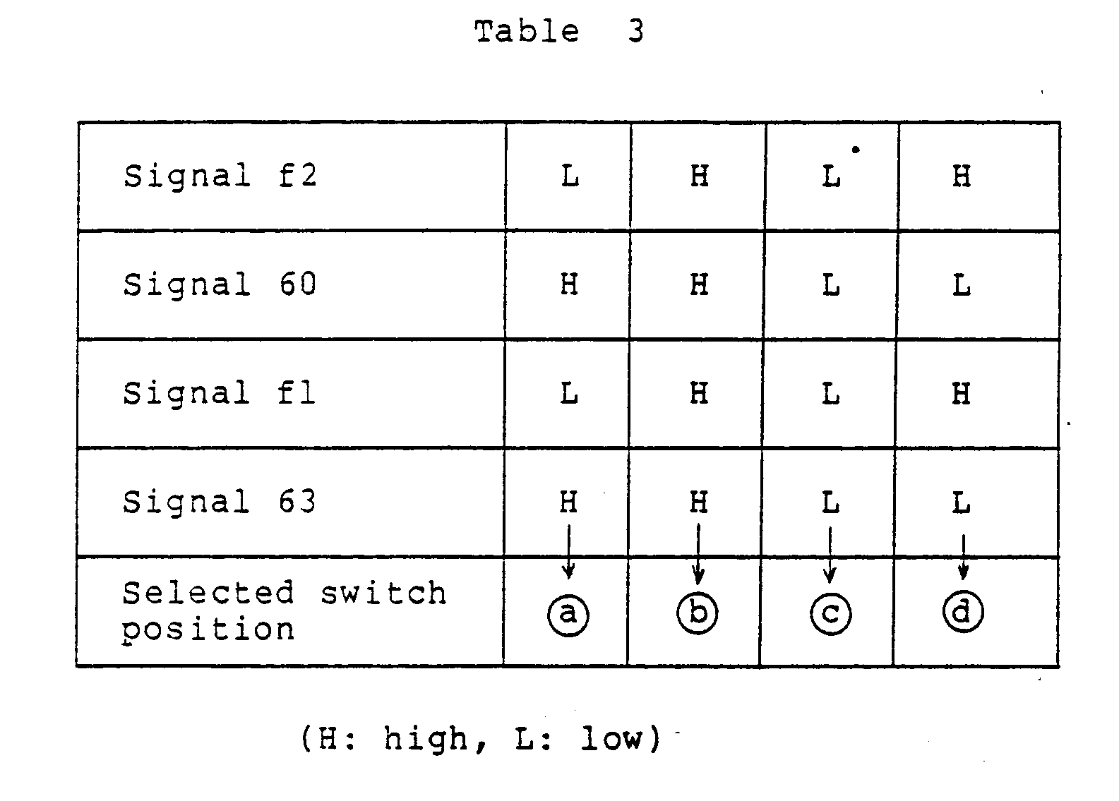
According to the outputs f1 and f2 of thefield discrimination circuits memory areas 60a-60d and reading from any ofmemory areas 60a-60d in thememory area 60 are controlled. In the preceding example, with the phase relationship between the main and sub-field video signals shown in Fig. 7, the time difference between reading and writing of a memory area is greater than 1-field scanning length. In the phase relationship shown in Fig. 6, the time difference between reading and writing is short, but in this case reading always precedes writing for a memory area. For example, at time t1 in Fig. 6, the signal f2 and signal 60 are both low, causing the write switch 11a to position to ⓒ-terminal, as indicated in Table 3, while the signal f1 and signal 63 are both high, causing the switch 11a to turn to ⓑ-terminal. At the time point when the scanning has reached the sub-field al as shown in thescreen 16a of Fig. 5, the bl information for the screen 18b is written in the memory, but in this case reading takes place for thememory area 60d are writing takes place for thememory area 60c. At time t2 in Fig. 6, the signals f2 and 60 go high, causing the switch 11a to turn to ⓑ-terminal. Reading and writing take place for thesame memory area 60c, but in the time band T5 reading for thememory area 60c always precedes, and therefore the writing phase never outruns the reading phase. Reading of thememory area 60c completes at time t3, and a short while later following the end of the time band T1, writing of thememory area 60c completes. For the same memory area, the reading phase and writing phase becomes closest when the signals f2, 60 and 63 rise coincidently (at this time the signal f1 is fixed to high), but even under this condition reading always precedes writing except for a coincident moment at the beginning of reading and writing for a memory area. Accordingly, the outrun phenomenon can be prevented by the present invention. - Next, a specific arrangement and operation of the
field discrimination circuit 303 and falseoperation preventing circuit 305 shown in Fig. 8 will be described. In the figure, shown by 303a is a horizontal sync separator, 303b is a vertical sync separator, 303c is a pulse generating circuit, 303d is a reversible counter, 303e is a logic circuit, 303f is a flip-flop, 305a is a frequency division counter, and 305b is a discrimination circuit. Shown by 134 is a preset pulse applied to thereversible counter reversible counter 303d. - The operation of the above arrangement will be described with reference to the principal signal waveforms shown in Figs. 9 and 10. The sync-separated
signal 130 is fed to the horizontal sync separator 303a andvertical sync separator 303b, by which ahorizontal sync signal 131 andvertical sync signal 132 are extracted. The number of pulses of thehorizontal sync signal 131 in the outside of the period of thevertical sync signal 132 varies in each field, and the number of pulses of the horizontal sync signal within the vertical sync signal period (a, b, c) also varies in each field. It is a matter of choice to count the number of pulses of thehorizontal sync signal 131 inside or outside of the vertical sync period, but in this embodiment to save the bits count, the number of pulse of thehorizontal sync signal 131 within the vertical sync period (a, b, c) is counted. For this purpose, the pulse generating circuit 303c extractshorizontal sync pulses 133 within the vertical sync periods a, b and c, and supplies them as a clock to thereversible counter 303d. Thereversible counter 303d reveals the difference ofhorizontal sync pulses 133 among the consecutive vertical sync periods a, b and c. Namely, the circuit bases the field discrimination on the difference ofhorizontal sync pulses 133 in consecutive vertical sync periods. - The field discrimination operation will be described in more detail in the following. The flip-
flop 303f doubles the period of thevertical sync signal 132, and the first horizontal sync pulse (e) during the high period of that vertical sync signal and following the falling of the original vertical sync signal is used to make a latchingpulse 134, and the subsequent horizontal sync pulse (d) is used to make apresetting pulse 135. In this embodiment, thereversible counter 303d is made up of three bits having bit outputs Q1, Q2 and Q3, and the counter is preset to have '111' on the Q1, Q2 and Q3, i.e., a preset value of '7'. Thereversible counter 303d is designed to up-count in response to a high output signal (f1) from the flip-flop 303f and down-count in response to a low output signal f1. Under these operating conditions, thereversible counter 303d which has been preset to value '7' in response to thepreset pulse 135 at time point d operates to down-count (because of the low signal 136) thehorizontal sync pulses 133 within the period of the nextvertical sync signal 132. Accordingly, thecounter 303d down-counts from '7' to '6' to '5' and to '4' as shown by 137 in Fig. 9, and in the next vertical sync period c up-counts thepulses 133 from '5' to '6' to '7' and to '0'. The count value is latched in response to thelatch pulse 134 at e. - When the
signal 136 goes high in periods (a and c) including a larger number of horizontal sync pulses among the vertical sync periods a, b and c, as in the above case, the latched count value is rendered zero. In another case shown in Fig. 10, where the vertical sync periods a, b and c includehorizontal sync pulses 133 in '3', '4' and '3' in number, respectively, the latched count value when thesignal 136 goes low in the period (b) including a larger number of horizontal sync pulses is '7'. The above latching operation and discrimination of the count value are the role of thelogic circuit 303e, and it suffices to determine whether the latched value of Q3 is high or low. - If the
signal 136 in Figs. 9 and 10 is used as the field discrimination signal f1, one of the cases of Figs. 19 and 20 is a false judgement, and therefore the phase of the flip-flop 303f is unchanged or unchanged or inverted depending on this judgement result. In this case, single judgement result can be erroneous due to a noise component on the sync signals, and therefore it is desirable to make a final decision using several judgement results. The falseoperation preventing circuit 305 is provided for this purpose, and it includes a decision circuit 305b which makes a final decision upon consistent results of count for the vertical sync signal 132 (or signal 136) by thecounter 305a. The flip-flop 303f is controlled to reverse upon successive false decisions in several count operations, and the noise immunity of the operation can be enhanced significantly. - As for the switching
control circuit 5 in Figs. 1 and 2, it serves to exchange the main-field and sub-field in 2-field display. The circuit is operated in synchronism with the vertical sync signal to gain the smoothness. Since the circuit can be arranged using known means, and its detailed explanation will be omitted. - According to the foregoing embodiments of this invention, 2-field patches at the top and bottom of the screen, which has occurred in the conventional 2-field display system in displaying a sub-field due to outrun of read/write phases, can be eliminated, and a sub-field display can be a complete 1-field picture even in the case of fast motion, whereby the performance can effectively be improved.
Claims (4)
- An image processing system for compressing a sub-field picture signal by using a memory (12) for storing picture information of the sub-field picture signal and for outputting the compressed sub-field picture signal synthesized - in a signal merging unit (26) - with a main-field picture signal, wherein the memory (12) is a dual-port memory having a first port and a second port and implementing its reading operation and its writing operation in asynchronous manner,
characterized by,
field discriminating means (303, 304) which discriminates odd-numbered and even-numbered fields of the main-field video signal and the sub-field video signal,
memory address control means (306) for controlling the writing of said sub-field picture information into a certain area of said memory means (12) according to the result of said field discrimination of the sub-field picture
and for controlling the read-out of stored information from a selected one of said areas in response to the result of said field discrimination of both the main-field and sub-field picture. - An image processing system according to claim 1, wherein said memory (12) is capable of storing four fields of sub-field video signals, and the system further comprises,
divider means for dividing the discriminating sub-field video signals;
displaying period control means (306b) which outputs a displaying period signal of the sub-field video signals;
merging means with merges main-field video signals and sub-field video signals for output in accordance with the controlled displaying period signal;
said memory address control means (306) comprising write address control means for deciding an address area in said memory to write information in accordance with the discriminated sub-field video signals and the divided sub-field video signals and;
read address control means for deciding the read address area in the memory according to said discriminating main field video signals, the displaying period signal and said divided sub-field video signals. - An image processing system according to claim 1, wherein each of said field discriminating means for main-field and sub-field video signals comprises;
a reversible counter which counts the number of horizontal sync signals inside or outside a vertical sync signal period of the image and sub-field video signals, means for presetting said reversible counter once in N periods (where N is a positive integer) of the vertical sync signal, sample-holding means which samples and holds the contents of said reversible counter immediately before presetting, second frequency-division means which implements frequency division for the vertical sync signal, and frequency division phase control means which varies the frequency-division phase of said second frequency-division means in accordance with the output of said sample holding means. - An image processing system according to claim 3, further comprising
a counter for counting the vertical sync signal or the output of said second frequency-division means, variation detection means which detects whether or not the output of an sample-holding means varies during a certain count period of said counter, and means for operating on said frequency-division phase only at the detection of variation by said variation detecting means.
Applications Claiming Priority (4)
| Application Number | Priority Date | Filing Date | Title |
|---|---|---|---|
| JP106609/86 | 1986-05-12 | ||
| JP61106609A JPS62264775A (en) | 1986-05-12 | 1986-05-12 | Image processor |
| JP112604/86 | 1986-05-19 | ||
| JP11260486A JPH07101931B2 (en) | 1986-05-19 | 1986-05-19 | Image processing device |
Publications (3)
| Publication Number | Publication Date |
|---|---|
| EP0245745A2 EP0245745A2 (en) | 1987-11-19 |
| EP0245745A3 EP0245745A3 (en) | 1989-03-15 |
| EP0245745B1 true EP0245745B1 (en) | 1993-10-27 |
Family
ID=26446737
Family Applications (1)
| Application Number | Title | Priority Date | Filing Date |
|---|---|---|---|
| EP87106443A Expired - Lifetime EP0245745B1 (en) | 1986-05-12 | 1987-05-04 | Image processing system |
Country Status (4)
| Country | Link |
|---|---|
| US (1) | US4984083A (en) |
| EP (1) | EP0245745B1 (en) |
| KR (1) | KR910001654B1 (en) |
| DE (1) | DE3787923T2 (en) |
Families Citing this family (21)
| Publication number | Priority date | Publication date | Assignee | Title |
|---|---|---|---|---|
| US4724487A (en) * | 1987-02-17 | 1988-02-09 | Rca Corporation | Interlace inversion detector for a picture-in-picture video signal generator |
| JP2973420B2 (en) * | 1988-03-30 | 1999-11-08 | キヤノン株式会社 | Video camera |
| KR950010887B1 (en) * | 1988-07-08 | 1995-09-25 | Samsung Electronics Co Ltd | Multi-screen producting image control circuit |
| GB2236031B (en) * | 1989-06-30 | 1993-11-17 | Samuelson Group Plc | Video mixer unit |
| US5208660A (en) * | 1989-07-29 | 1993-05-04 | Sharp Kabushiki Kaisha | Television display apparatus having picture-in-picture display function and the method of operating the same |
| KR910013904A (en) * | 1989-12-21 | 1991-08-08 | 강진구 | POP playback TV using HD screen |
| JPH03204283A (en) * | 1989-12-29 | 1991-09-05 | Nec Corp | Slave pattern information storage circuit |
| US5369444A (en) * | 1990-06-01 | 1994-11-29 | Thomson Consumer Electronics | Field type matching system |
| GB9012326D0 (en) * | 1990-06-01 | 1990-07-18 | Thomson Consumer Electronics | Wide screen television |
| US5287189A (en) * | 1992-08-21 | 1994-02-15 | Thomson Consumer Electronics, Inc. | Displaying an interlaced video signal with a noninterlaced video signal |
| US20040230992A1 (en) * | 1993-05-27 | 2004-11-18 | Gemstar Development Corporation | Method and apparatus for displaying video clips |
| US6002444A (en) | 1994-05-20 | 1999-12-14 | United Video Properties, Inc. | Video clip program guide |
| US5523796A (en) * | 1994-05-20 | 1996-06-04 | Prevue Networks, Inc. | Video clip program guide |
| MY118491A (en) * | 1995-06-02 | 2004-11-30 | Matsushita Electric Industrial Co Ltd | A subpicture image signal vertical compression circuit |
| JPH0983893A (en) * | 1995-09-08 | 1997-03-28 | Matsushita Electric Ind Co Ltd | Television receiver |
| KR100186409B1 (en) * | 1996-04-23 | 1999-05-01 | 구자홍 | Circuit for processing pip image signal suitable type in the tv and pc |
| TW374155B (en) * | 1997-05-27 | 1999-11-11 | Sony Corp | Image compression device and image compression method |
| EP1292133A1 (en) * | 2001-09-06 | 2003-03-12 | Koninklijke Philips Electronics N.V. | Multi-picture display |
| KR100463531B1 (en) * | 2002-10-11 | 2004-12-29 | 엘지전자 주식회사 | Apparatus for processing main/sub image in digital TV |
| JP5672862B2 (en) | 2010-08-27 | 2015-02-18 | ソニー株式会社 | Imaging apparatus, imaging system, and imaging method |
| KR101573916B1 (en) * | 2014-12-16 | 2015-12-02 | (주)넥스트칩 | Method and apparatus for receiving vedio |
Family Cites Families (11)
| Publication number | Priority date | Publication date | Assignee | Title |
|---|---|---|---|---|
| GB1576621A (en) * | 1976-03-19 | 1980-10-08 | Rca Corp | Television synchronizing apparatus |
| DE2644706C3 (en) * | 1976-10-04 | 1985-12-05 | Robert Bosch Gmbh, 7000 Stuttgart | System for the transmission or storage of a color television signal |
| DE2725362C3 (en) * | 1977-06-04 | 1980-08-28 | Robert Bosch Gmbh, 7000 Stuttgart | Method for processing color television signals |
| JPS5492015A (en) * | 1977-12-29 | 1979-07-20 | Matsushita Electric Ind Co Ltd | Color television image receiving unit |
| JPS6053940B2 (en) * | 1978-05-19 | 1985-11-28 | 株式会社東京放送 | Write prohibition control circuit in frame synchronizer |
| US4249213A (en) * | 1978-09-14 | 1981-02-03 | Hitachi, Ltd. | Picture-in-picture television receiver |
| JPS5637778A (en) * | 1979-09-04 | 1981-04-11 | Sony Corp | Producing circuit of inserted screen signal |
| US4562435A (en) * | 1982-09-29 | 1985-12-31 | Texas Instruments Incorporated | Video display system using serial/parallel access memories |
| US4623915A (en) * | 1984-09-21 | 1986-11-18 | Rca Corporation | Apparatus for processing multiple time division multiplexed asynchronous composite video signals |
| US4656515A (en) * | 1985-03-25 | 1987-04-07 | Rca Corporation | Horizontal compression of pixels in a reduced-size video image utilizing cooperating subsampling and display rates |
| US4665438A (en) * | 1986-01-03 | 1987-05-12 | North American Philips Corporation | Picture-in-picture color television receiver |
-
1987
- 1987-05-04 EP EP87106443A patent/EP0245745B1/en not_active Expired - Lifetime
- 1987-05-04 DE DE3787923T patent/DE3787923T2/en not_active Expired - Fee Related
- 1987-05-07 KR KR1019870004461A patent/KR910001654B1/en not_active Expired
-
1989
- 1989-06-28 US US07/373,630 patent/US4984083A/en not_active Expired - Lifetime
Also Published As
| Publication number | Publication date |
|---|---|
| EP0245745A3 (en) | 1989-03-15 |
| DE3787923T2 (en) | 1994-05-26 |
| KR910001654B1 (en) | 1991-03-16 |
| KR870011790A (en) | 1987-12-26 |
| EP0245745A2 (en) | 1987-11-19 |
| DE3787923D1 (en) | 1993-12-02 |
| US4984083A (en) | 1991-01-08 |
Similar Documents
| Publication | Publication Date | Title |
|---|---|---|
| EP0245745B1 (en) | Image processing system | |
| US4364090A (en) | Method for a compatible increase in resolution in television systems | |
| US4249213A (en) | Picture-in-picture television receiver | |
| KR940006625B1 (en) | Adaptive field or frame store processor | |
| CA1173954A (en) | Television receiver including a circuit for doubling line scanning frequency | |
| KR950014577B1 (en) | Pip signal control method & apparatus of hdtv | |
| EP0490942A1 (en) | Multiple hdtv format digital signal converter | |
| JPS63256071A (en) | Video signal generating circuit of picture-in-picture | |
| US5045939A (en) | Apparatus utilizing motion detector for converting a maximum motion portion of a wide screen tv signal to a normal screen tv signal | |
| US4768095A (en) | Apparatus for processing image | |
| JPS63104582A (en) | Television signal processing system | |
| US4782391A (en) | Multiple input digital video features processor for TV signals | |
| EP0363970B1 (en) | Flicker reduction apparatus | |
| US6226039B1 (en) | Automatic aspect ratio converting apparatus for television receiver | |
| KR100394288B1 (en) | Video picture display method and video display device of first and second received video signals | |
| US4722007A (en) | TV receiver having zoom processing apparatus | |
| US4991013A (en) | Picture-in-picture television apparatus with sync controlled memory addressing | |
| GB2248745A (en) | Picture signal superposing circuit | |
| US4907072A (en) | Mosaic picture generation circuit | |
| JP2692128B2 (en) | Image processing circuit | |
| JP2696988B2 (en) | Video signal processing device | |
| JP2860988B2 (en) | Image storage device | |
| JP3410117B2 (en) | Signal processing adapter | |
| JP3112078B2 (en) | Image storage device | |
| JP2681996B2 (en) | Image processing device |
Legal Events
| Date | Code | Title | Description |
|---|---|---|---|
| PUAI | Public reference made under article 153(3) epc to a published international application that has entered the european phase |
Free format text: ORIGINAL CODE: 0009012 |
|
| 17P | Request for examination filed |
Effective date: 19870504 |
|
| AK | Designated contracting states |
Kind code of ref document: A2 Designated state(s): DE FR GB |
|
| PUAL | Search report despatched |
Free format text: ORIGINAL CODE: 0009013 |
|
| AK | Designated contracting states |
Kind code of ref document: A3 Designated state(s): DE FR GB |
|
| 17Q | First examination report despatched |
Effective date: 19910604 |
|
| GRAA | (expected) grant |
Free format text: ORIGINAL CODE: 0009210 |
|
| AK | Designated contracting states |
Kind code of ref document: B1 Designated state(s): DE FR GB |
|
| REF | Corresponds to: |
Ref document number: 3787923 Country of ref document: DE Date of ref document: 19931202 |
|
| ET | Fr: translation filed | ||
| PLBE | No opposition filed within time limit |
Free format text: ORIGINAL CODE: 0009261 |
|
| STAA | Information on the status of an ep patent application or granted ep patent |
Free format text: STATUS: NO OPPOSITION FILED WITHIN TIME LIMIT |
|
| 26N | No opposition filed | ||
| REG | Reference to a national code |
Ref country code: GB Ref legal event code: IF02 |
|
| PGFP | Annual fee paid to national office [announced via postgrant information from national office to epo] |
Ref country code: FR Payment date: 20030423 Year of fee payment: 17 |
|
| PGFP | Annual fee paid to national office [announced via postgrant information from national office to epo] |
Ref country code: GB Payment date: 20030425 Year of fee payment: 17 |
|
| PGFP | Annual fee paid to national office [announced via postgrant information from national office to epo] |
Ref country code: DE Payment date: 20030605 Year of fee payment: 17 |
|
| PG25 | Lapsed in a contracting state [announced via postgrant information from national office to epo] |
Ref country code: GB Free format text: LAPSE BECAUSE OF NON-PAYMENT OF DUE FEES Effective date: 20040504 |
|
| PG25 | Lapsed in a contracting state [announced via postgrant information from national office to epo] |
Ref country code: DE Free format text: LAPSE BECAUSE OF NON-PAYMENT OF DUE FEES Effective date: 20041201 |
|
| GBPC | Gb: european patent ceased through non-payment of renewal fee |
Effective date: 20040504 |
|
| PG25 | Lapsed in a contracting state [announced via postgrant information from national office to epo] |
Ref country code: FR Free format text: LAPSE BECAUSE OF NON-PAYMENT OF DUE FEES Effective date: 20050131 |
|
| REG | Reference to a national code |
Ref country code: FR Ref legal event code: ST |