EP0187375B1 - Nonvolatile semiconductor memory device - Google Patents
Nonvolatile semiconductor memory device Download PDFInfo
- Publication number
- EP0187375B1 EP0187375B1 EP85116542A EP85116542A EP0187375B1 EP 0187375 B1 EP0187375 B1 EP 0187375B1 EP 85116542 A EP85116542 A EP 85116542A EP 85116542 A EP85116542 A EP 85116542A EP 0187375 B1 EP0187375 B1 EP 0187375B1
- Authority
- EP
- European Patent Office
- Prior art keywords
- lines
- row
- circuit
- decoder
- high voltage
- Prior art date
- Legal status (The legal status is an assumption and is not a legal conclusion. Google has not performed a legal analysis and makes no representation as to the accuracy of the status listed.)
- Expired
Links
- 239000004065 semiconductor Substances 0.000 title claims description 16
- 230000015654 memory Effects 0.000 claims description 49
- 238000007667 floating Methods 0.000 description 17
- 238000010586 diagram Methods 0.000 description 7
- 239000003990 capacitor Substances 0.000 description 6
- 230000004048 modification Effects 0.000 description 4
- 238000012986 modification Methods 0.000 description 4
- 238000010276 construction Methods 0.000 description 3
- 230000000717 retained effect Effects 0.000 description 3
- VYPSYNLAJGMNEJ-UHFFFAOYSA-N Silicium dioxide Chemical compound O=[Si]=O VYPSYNLAJGMNEJ-UHFFFAOYSA-N 0.000 description 2
- 239000000969 carrier Substances 0.000 description 2
- 230000008878 coupling Effects 0.000 description 2
- 238000010168 coupling process Methods 0.000 description 2
- 238000005859 coupling reaction Methods 0.000 description 2
- 238000001514 detection method Methods 0.000 description 2
- 238000005516 engineering process Methods 0.000 description 2
- 229910021420 polycrystalline silicon Inorganic materials 0.000 description 2
- 229910052814 silicon oxide Inorganic materials 0.000 description 2
- 239000000758 substrate Substances 0.000 description 2
- 230000003247 decreasing effect Effects 0.000 description 1
- 230000000694 effects Effects 0.000 description 1
- 238000002347 injection Methods 0.000 description 1
- 239000007924 injection Substances 0.000 description 1
- 239000011159 matrix material Substances 0.000 description 1
- 229910044991 metal oxide Inorganic materials 0.000 description 1
- 150000004706 metal oxides Chemical class 0.000 description 1
- 238000012856 packing Methods 0.000 description 1
- 230000004044 response Effects 0.000 description 1
Images


Classifications
-
- G—PHYSICS
- G11—INFORMATION STORAGE
- G11C—STATIC STORES
- G11C16/00—Erasable programmable read-only memories
- G11C16/02—Erasable programmable read-only memories electrically programmable
- G11C16/06—Auxiliary circuits, e.g. for writing into memory
- G11C16/10—Programming or data input circuits
- G11C16/12—Programming voltage switching circuits
-
- G—PHYSICS
- G11—INFORMATION STORAGE
- G11C—STATIC STORES
- G11C16/00—Erasable programmable read-only memories
- G11C16/02—Erasable programmable read-only memories electrically programmable
- G11C16/06—Auxiliary circuits, e.g. for writing into memory
- G11C16/08—Address circuits; Decoders; Word-line control circuits
Definitions
- This invention relates to a nonvolatile semiconductor memory device using nonvolatile memory cells.
- EEPROM Electrically erasable and programmable read only memories
- EPROM erasable and programmable read only memory
- Each nonvolatile memory cell can be structurally illustrated in the form of an MOS (metal oxide semiconductor) transistor, as shown in Figs. 1A to 1D.
- MOS metal oxide semiconductor
- 101 and 102 are source and drain regions, respectively.
- a floating gate electrode, denoted by 103 which is in an electrically floating state, is made of, for example, polycrystalline silicon.
- a control gate electrode, denoted by 104 is similarly made of, for example, polycrystalline silicon.
- a relatively thick insulating film of, for example, a silicon oxide film exists between floating gate electrode 103 and semiconductor substrate 105, and between floating gate electrode 103 arid control gate electrode 104.
- Relatively thin insulating film 107 of, for example, a silicon oxide film is formed on substrate 105, where floating gate electrode 103 closes drain region 102.
- Data is set into the memory cell by injecting electrons into floating gate 103 of the cell.
- the threshold value of the cell transistor is high. Consequently, even if a high voltage is applied to control gate 104, the transistor is not turned on.
- the cell transistor is turned on, providing a high voltage is applied to control gate 104.
- "1" or "0" data of the cell is determined.
- a high voltage is applied to control gate 104. As a result of the application of this high potential, the potential at floating gate 103 is increased through the capacitor coupling between control gate 104 and floating gate 103.
- the memory device comprises memory cells arranged in a matrix fashion.
- a high voltage must be selectively applied to the control gate electrode.
- some of the memory devices contain boost circuits.
- a power source voltage of 5 V for example, can be boosted to, for example, 20 V.
- An example of such a boost circuit is shown in Fig. 2.
- Timing charts of pulse signals ⁇ 1 and ⁇ 2, used to control the operation of the boost circuit, are shown in Figs. 3A and 3B.
- the known boost circuit comprises a plurality of enhancement type MOS transistors 201 serving as diodes, and a plurality of capacitors 202.
- the boost circuit can boost a 5 V power source voltage Vc to as high a voltage V H as 20 V, for example.
- This 20 V high voltage V H provides only a weak current.
- no current must be fed from the boost circuit to the nonselected memory cells: those memory cells whose control gate electrodes are grounded. Instead, the boosted voltage must be applied to the selected memory cells.
- Such a data write circuit needs an increased number of circuit elements; hence its construction is complicated.
- the conventional memory device is provided with a data write circuit for each row or column line, the memory device contains a large number of elements. Consequently, when fabricating an integrated circuit, the resultant chip is large in size.
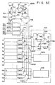
- FIG. 4 A circuit diagram of a conventional EPROM is shown in Fig. 4.
- Memory cells TM11 to TMmn as MOS transistors of the double layered gate (floating and control gates) structure, are located at the cross points of row lines R1 to Rm and column lines D1 to Dn.
- the sources of memory cells TM11 to TMmn are all grounded.
- Memory cells TM11 to TMmn cooperate to form memory cell array 10.
- Row lines R1 to Rm are connected to row decoder 20 through depletion type (D type) MOS transistors TR1 to TRm.
- Control signal R/ W is applied to the gates of transistors TR1 to TRm to control data read/write.
- Row decoder 20 receives a row address signal (not shown) and selects one of the row lines accordingly, and sets the selected line to a high potential.
- Column lines D1 to Dn are connected to signal detection node N1, through enhancement type (E type) MOS transistors TD1 to TDn.
- Sense amplifier 40 is connected to node N1.
- Output circuit 50 is connected to amplifier 40.
- a signal at node N1 is detected by amplifier 40 and output to the exterior through output circuit 50.
- Column select lines C1 to Cn are connected to the gates of transistors TD1 to TDn, respectively. Lines C1 to Cn are connected to column decoder 60 through D type MOS transistors TC1 to TCn. Control signal R/ W is applied to the gates of transistors TC1 to TCn. Decoder 60 selects one of column select lines C (generally designated as C1 to Cn) according to a column address signal, and sets it to a high potential.
- Write circuit 70 selectively feeds high voltage V H to row line R (generally designates R1 to Rm) and column select line C.
- Voltage V H is for writing data, and is obtained by the voltage boost circuit of Fig. 2.
- Boosted voltage distributing circuits 711 to 72m, of a total of (n+m), are provided to correspond to column select lines C1 to Cn and row lines R1 to Rm.
- Circuits 71 and 72 (generally designated as 711 to 71n and 721 to 72m) are each comprised of four D type MOS transistors TW1 to TW4, and one E type MOS transistor TW5, as typified by circuit 721 which is connected to row line R1.
- transistors TW1 and TW2 are connected to power source terminal 73, coupled with voltage V H , and power source terminal 74, coupled with power source voltage Vc of, for example, 5 V, respectively.
- the second ends of these transistors are connected together at node 75.
- Transistor TW3 is connected between node 75 and row line R1.
- the gates of both transistors TW1 and TW3 are connected together to row line R1.
- Transistors TW4 and TW5 are inserted in series between terminal 76, connected to voltage Vc, and the ground potential point. Connection point 77, between these transistors, is connected to the gates of transistors TW2 and TW4.
- the gate of transistor TW5 is connected to row line R1.
- E type MOS transistor T1 is connected between node N1 and terminal 78 which is connected to voltage V H .
- the gate of transistor T1 is supplied with a signal appearing at output node N2 of write data input control circuit 80.
- Circuit 80 is comprised of power source terminal 82, NAND gate circuit 83, and voltage output control circuit 84.
- NAND gate 83 includes D type MOS transistor T2 and E type MOS transistors T3 and T4, which are connected in series between ground and power source terminal 82 which is connected to voltage Vc.
- Voltage output control circuit 84 includes D type transistors TW11 to TW13, and E type transistor TW14, and controls voltage V H according to a signal appearing at output node N3 of NAND gate circuit 83.
- the gate of transistor T2 is connected to its output node N3.
- the gate of transistor T3 is supplied with input data Din.
- the gate of transistor T4 is supplied with signal R /W which is set at level "1" in a write mode and at "0" in a read mode.
- signal R/ W is set at high ("1") level, signal R /W at low (“0") level, and voltage V H at power source terminal 73 at 5 V.
- signal R/ W is high in level, transistors TC1 to TCn, and transistors TR1 to TRm are turned on.
- signal R /W is low, transistor T4 is turned off, the signal at output node N3 of NAND circuit 83 is set to high level, the signal at output node N2 of output control circuit 84 is set to low level, and transistor T1 is turned off.
- memory cell TM (generally designated as TM11 to TMmn) in memory cell array 10, located at this intersecting point, is selected. If no carriers are injected into selected memory cell TM, the memory cell is turned on, allowing current to flow between the drain and source. If carriers are injected into selected memory cell TM, the memory cell is turned off and signal detecting node N1 is set to high level by the load in sense amplifier 40. The signal at node N1 at this time is output to the exterior through sense amplifier 40 and output circuit 50.
- signal R/ W When "1" level data is written into the cell, signal R/ W is set to low level, signal R /W to high level, and voltage V H to positive 20 V. At this time, if row line R1 and column select line C1, for example, are selected, the "1" level voltage is applied to row line R1 and column select line C1, through transistors TR1 and TC1. Then, boosted voltage distribution circuits 711 and 722, connected to row line R1 and column select line C1, produce high voltage V H . Row line R1 and column select line C1 are charged up to 20 V.
- the high voltage is applied to the control gates of memory cell TM11, selected by row and column lines R1 and D1, and subsequently, to its drain, with the result that data of "1" level is written into memory cell TM11 by the injection of electrons caused by the tunnel effect. If input data Din is set to low level, the transistor T1 is turned off, so that high voltage is not applied to the drain of memory cell TM11. Accordingly, data of "1" level is not written into the cell (This operation is equivalent to the writing of "0" level into the cell).
- the cell data is nonvolatile.
- the conventional nonvolatile semiconductor memory device needs boosted voltage distribution circuits for each row line and each column select line. This results in an increase in the number of circuit elements required for the memory device as a whole, resulting in reduction of packing density when the device is fabricated by IC technology.
- GB-A-2 094 086 describes a non-volatile semiconductor memory system including a memory cell array having floating gate type MOS transistors, and a boosting circuit for boosting a write voltage applied to the memory system.
- a distributing circuit is further contained for selectively distributing a boosted voltage from the boosting circuit to at least a part of the memory system, for example, row lines in response to a control signal.
- Distributing circuits may be responsive to the state of address lines such that the boosted voltage is only applied to the selected row and column, thereby reducing power requirements.
- an object of the present invention is to provide a nonvolatile semiconductor memory device in which the number of necessary high voltage supply circuits has been decreased.
- a nonvolatile semiconductor memory device comprising: a plurality of row lines ; a plurality of column lines crossing said plurality of row lines to define intersections therebetween; a memory array comprising a plurality of memory cells (TM11-TMmn), said plurality of memory cells being located on said intersections; a plurality of column selecting lines connected to said column lines; a first decoder for receiving an address signal and for selecting one of said row lines and one of said column selecting lines; and high voltage supply means for providing a high voltage to said memory cells, characterized by: a plurality of selecting elements grouped into a plurality of groups, one terminal of said selecting elements being connected to said row lines or said column selecting lines, said high voltage supply means comprising a plurality of high voltage supply circuits provided for said groups of said selecting elements, one of said high voltage supply circuits being connected to the other terminal of those of said selecting elements which constitute a group, and a second decoder for receiving said address signal and for selecting one of said selecting elements.
- FIG. 5A to 5D An EPROM according to an embodiment of the present invention will be described with reference to Figs. 5A to 5D.
- This embodiment differs from the EPROM shown in Fig. 4 in the following respects. While the conventional circuit shown in Fig. 4 uses boosted voltage distribution circuits for each row line or each column select line, the circuit of this embodiment, shown in Figs. 5A to 5D, uses one boosted voltage distribution circuit for four column select lines or four row lines. Further, decoders 901 to 904 are additionally provided.
- memory cells TM11 to TMmn - MOS transistors of a double gate (floating and control gates) structure - are located at the intersections of row lines R1 to Rm and column lines D1 to Dn.
- the sources of memory cells TM11 to TMmn are all grounded.
- Memory cells TM11 to TMmn cooperate to form memory cell array 10.
- Row lines R1 to Rm are connected to row decoder 20 through depletion type (D type) MOS transistors TR1 to TRm.
- Control signal R/ W for control of data read/write, is applied to the gate of transistors TR1 to TRm.
- Row decoder 20 receives a row address signal (not shown), selects one of the row lines according to the contents of the address signal, and sets the line at a high potential.
- Column lines D1 to Dn are connected to signal detection node N1 through column selection enhancement type (E type) MOS transistors TD1 to TDn.
- Sense amplifier 40 is connected to node N1.
- Output circuit 50 is connected to amplifier 40.
- a signal at node N1 is detected by amplifier 40 and output to the exterior through output circuit 50.
- Column select lines C1 to Cn are connected to the gates of transistors TD1 to TDn, respectively. Lines C1 to Cn are connected to column decoder 60 through D type MOS transistors TC1 to TCn. Control signal R/ W is applied to the gates of transistors TC1 to TCn. Decoder 201 receives a column address signal (not shown), selects one of column select lines C (generally designated as C1 to Cn) according to the column address signal, and sets it to a high potential.
- Write circuits 70R and 70C are used to supply high voltage Vp to row lines R and column lines C, when data is to be written into memory cells TM11 to TMmn.
- Write circuit 70R comprises boosted voltage distributing-circuits 72R1 to 72Ri.
- lines R1 to R4 are connected together to single boosted voltage distribution circuit 72R1 through node N5 and E type MOS transistors TWR11 to TWR14.
- Row lines R5 to R8 are connected together to boosted voltage distribution circuit 72R2 through E type MOS transistors TWR21 to TWR24.
- four row lines R are connected together to one boosted voltage distribution circuit 72R through four E type MOS transistors TWR.
- Row lines Rm-3 to Rm are connected together to one boosted voltage distribution circuit 72Ri through E type MOS transistors TWRi1 to TWRi4.
- the structure and operation of the boosted voltage distributing circuits 72C1 to 72Ci are substantially the same as those of boosted voltage distributing circuits 72R1 to 72Ri, except that circuits 72C1 to 72Ci are connected to groups of the four column select lines C1, C2, C3, C4; ...; C n-3 , C n-2 , C n-1 , Cn. Therefore, corresponding characters with the suffix C are employed, and the descriptions are omitted.
- Signal H1, derived from decoder 901 is applied to the gates of transistors TWR11, TWR21, ..., TWRi1.
- signal H2, derived from decoder 902 is applied to the gates of transistors TWR12, TWR22, ..., TWRi2.
- Signal H3, derived from decoder 903 is connected to the gates of transistors TWR13, TWR23, ..., TWRi3.
- Signal H4, coming from decoder 904 is applied to the gates of transistors TWR14, TWR24, ... TWRi4.
- Decoders 901 through 904 have the same configurations. As typified by decoder 904, each circuit comprises D type MOS transistor T11 for load, NAND gate circuit 92, and voltage output control circuit 93.
- the source-drain path of transistor T11 is inserted between power source terminal 91, coupled with voltage Vc, and node N11.
- the gate of transistor T11 is connected to node N11.
- E type MOS transistors T12 to T14 are connected in series between node N11 and ground potential.
- Two bit row address signals RA1 and RA2 are applied to the gates of transistors T12 and T13.
- Signal R /W is applied to the gate of transistor T14. This signal is in "0" level in the read mode and in "1" level in the write mode.
- Control circuit 93 is made up of D type transistors TW11 to TW13, and E type transistor TW14. This circuit is configured like voltage output control circuit 84.
- the signal from output node N11 of NAND gate circuit 92 is
- Decoders 902 to 904 are similarly configured. In decoder 903, signals RA1 and RA2 are used in place of address signals RA1 and RA2. In decoder 902, signals RA1 and RA2 are used in place of address signals RA1 and RA2. In decoder 901, signals RA1 and RA2 are used in place of signals RA1 and RA2.
- address signals RA1 and RA2 are the same as the address signals applied when row decoder 20 selects row lines R1, R5, ... , Rm-3.
- Signals RA1 and RA2 are the same as the address signals applied when row decoder 20 selects row lines R2, R6, ..., Rm-2.
- Signals RA1 and RA2 are the same as the address signals applied when row decoder 20 selects row lines R3, R7, ..., Rm-1.
- Signals RA1 and RA2 are the same as the address signals applied when row decoder 20 selects row lines R4, R8, ..., Rm.
- row decoder 20 is constructed with a NOR gate type circuit, it needs only to invert the phases of all of the address signals. That is to say, the address signals to select row lines R1, R5, ..., Rm-3 are RA1 and RA2, respectively.
- signal R/ W is set at high level, signal R /W at low level, and voltage VH at 5 V.
- signal R /W is set at "0" level.
- transistors T14 in decoders 901 to 904 are all turned off. Node N11 is then set to "1" level. Therefore, transistors T14 of voltage output control circuits 93 in decoders 901 to 904 are turned on, so that signals H1 to H4 are "0" in level.
- selected transistors TWR11 to TWR14, TWR21 to TWR24, ..., TWRi1 to TWRi4 are all turned off, so that lines R1 to Rm are selectively driven by the output signal of row decoder 20.
- transistors T14 in decoders 901 to 904 are all turned on. At this time, if one row line R4 is selected, transistors T12 and T13 are both in an on state. Transistors T12 and T13 contained in decoder 904 are supplied with row address signals RA1 and RA2 same as those supplied to row decoder 20 when row line R4 is selected. As a result, only the signal at output node N11 of NAND gate circuit 92 in decoder 904 is set to "0" level. In turn, transistor TW12 in voltage output control circuit 93 is turned on, and signal H4 is set to "1" level. Further, the gate of transistor TW11 is substantially 0 V.
- transistor TW11 is turned off. High voltage VH is applied to output node N12 through transistors TW12 and TW13. At this time, either of transistors T12 and T13 is turned off in each of decoders 901 to 903.
- the signal at output node N11 of NAND gate circuit 92 is set to "1" level, so that transistor TW14 is turned on. Therefore, signals H1 to H3 are all in "0" level. By this time, in decoder 901 to 903, high voltage VH has been applied to transistor TW12.
- row lines R5 through R8 are disconnected from boosted voltage distribution circuit 72R2 by select transistors TWR21 to TWR23. Only row line R8 is connected, through transistor TWR24, to distribution circuit 72R2. Because, row line R8 has not been selected by row decoder 20, it is set in "0" level, and no high voltage is applied to it from distribution circuit 72R2. The same thing is true for other groups of other four row lines (for example, a group of row lines R1 through R4). Consequently, no current is caused by the high voltage in distribution circuits 72R2 to 72Ri.
- one boosted voltage distribution circuit is provided for each group of four row lines R1 through R4, R5 through R8, ... and Rm-3 through Rm.
- one boosted voltage distribution circuit is provided for each of four column select line groups C1 through C4 and C5 through C8, .... Therefore, the number of the boosted voltage distribution circuits can be reduced to one quarter that of the conventional memory device.
- four decoder 90 are additionally provided.
- the number of row lines R is extremely large, and hence the number of distribution circuits is considerably large. For this reason, the number of circuit elements is considerably reduced for the entire memory device. This indicates that the memory device, when fabricated into an integrated circuit, requires a reduced size of the chip.
- Fig. 6 shows a modification of distribution circuit 72R in the device of Figs. 5A to 5D.
- voltage boost circuit 304 is used in place of circuit 72R.
- Circuit 304 is comprised of E type transistors 301 and 302 and capacitor 303. Circuit 304 is provided for each four row line group. One end of capacitor 303 is coupled with the output signal of oscillator 400 through inverter 305 which is supplied with high voltage Vp.
- the output signal of oscillator 400 is converted into signal ⁇ of high voltage Vp by inverter 305, and is fed to one end of capacitor 303 in boost circuit 304.
- voltage Vp as applied through transistor 301 and through the capacitive coupling of capacitor 303 is boosted.
- the boosted voltage is rectified by transistor 302 and supplied to one row line R.
- Figs. 7A to 7D show a semiconductor memory device according to another embodiment of the invention.
- the structure of boosted voltage distributing circuits 72R to 72C are different from those in the device of Figs. 5A to 5D. Others are substantially the same as those in the device of Figs. 5A to 5D.
- boosted voltage distributing circuit 72R1 comprises power source terminal 71 to which write voltage Vp is applied, D type MOS transistor TW101 whose drain is connected to power source terminal 71, E type MOS transistors TWR11 to TWR14 whose drains are connected to the source of MOS transistor TW101 and whose sources are connected to row lines R1 to R4.
- Other boosted voltage distributing circuits 72R2, 72R3, ..., and 72Ri have substantially the same construction as that of boosted voltage distributing circuits 72R1.
- boosted voltage distributing circuits 72R2 comprises power source terminal 71 to which write voltage Vp is applied, D type MOS transistor TW101 whose drain is connected to power source terminal 71, E type MOS transistors TWR21 to TWR24 whose drains are connected to the source of MOS transistor TWR101 and whose sources are connected to row lines R5 to R8.
- Boosted voltage distributing circuits 72Ri comprises power source terminal 71 to which write voltage Vp is applied, D type MOS transistor TW101 whose drain is connected to power source terminal 71, E type MOs transistors TWRi1 to TWRi4 whose drains are connected to the source of MOS transistor TW101 and whose sources are connected to row lines Rm3 to RM.
- Boosted voltage distributing circuit 72C1 comprises power source terminal 71 to which write voltage Vp is applied, D type MOB transistor TW101 whose drain is connected to power source terminal 71, E type MOS transistors TWRC11 to TWRC14 whose drains are connected to the source of MOS transistor TW101 and whose sources are connected to column select lines C1 to C4.
- Other boosted voltage distributing circuits 72C are substantially the same construction as that of boosted voltage distributing circuits 72C1 and the descriptions are omitted.
- transistors T14 in decoders 901 to 904 are all turned on. At this time, if one row line R4 is selected, transistors T12 and T13 are both in an on state.
- the transistors T12 and T13 contained in decoder 904 are supplied with row address signals RA1 and RA2 same as those supplied to row decoder 20 when row line R4 is selected.
- RA1 and RA2 row address signals
- transistors TW11 and TW14 in voltage output control circuit 93 is turned off, and signal H4 is set to "1" level (VH).
- row lines R5 to R8 are disconnected from load resistors TW101 in boosted voltage distribution circuit 72R2 by select transistors TWR21 to TWR23. Only row line R8 is connected, through transistor TWR24, to distribution circuit 72R2. By this time, row line R8 has not been selected by row decoder 20, it is set in "0" level. The same thing is true for other groups of other four row lines (for example, a group of row lines R1 through R4).
- Fig. 8 shows a modification of the decoder 904 in the device of Figs. 7A to 7D.
- the modified circuit 964 is of NOR gate type and comprises D type MOS transistor T21 and E type MOS transistors T21 to T24.
- Transistors T21 and T23 are inserted in series between write voltage terminal 97, to which write voltage Vp is applied, and ground.
- Transistors T22 and T24 are connected in parallel to transistor T23.
- the gates of transistors T22 and T23 are inputted with row address signals RA1 and RA2, respectifely.
- the gate of transistor T24 is in putted with read/write control signal R/ W .
- a high voltage H4 is taken out at the common node of transistor T22 to T24.
- the invention can be modified in that, for example, three bit row address signals may be used.
- eight row and/or column select lines are gathered into a single group of lines.
- One distribution circuit is provided for each group of lines. Further, the distribution circuits are applicable for only one of the row and column lines.
- the present invention can provide the EPROM and EEPROM of which chip size is smaller than that of the conventional one when the memory device of the invention is fabricated by the IC technology.
Landscapes
- Read Only Memory (AREA)
Description
- This invention relates to a nonvolatile semiconductor memory device using nonvolatile memory cells.
- Electrically erasable and programmable read only memories (EEPROM) or erasable and programmable read only memory (EPROM) using nonvolatile memory cells have long been known. Each of the memory cells has a double layered gate structure comprising a floating gate and a control gate. Data can be electrically written into and erased from the memory cells.
- Each nonvolatile memory cell can be structurally illustrated in the form of an MOS (metal oxide semiconductor) transistor, as shown in Figs. 1A to 1D. In Figs. 1A through 1D, 101 and 102 are source and drain regions, respectively. A floating gate electrode, denoted by 103, which is in an electrically floating state, is made of, for example, polycrystalline silicon. A control gate electrode, denoted by 104, is similarly made of, for example, polycrystalline silicon. A relatively thick insulating film of, for example, a silicon oxide film, exists between
floating gate electrode 103 andsemiconductor substrate 105, and betweenfloating gate electrode 103 aridcontrol gate electrode 104. Relatively thininsulating film 107 of, for example, a silicon oxide film, is formed onsubstrate 105, where floatinggate electrode 103 closesdrain region 102. - Data is set into the memory cell by injecting electrons into floating
gate 103 of the cell. When electrons are injected intofloating gate 103, the threshold value of the cell transistor is high. Consequently, even if a high voltage is applied tocontrol gate 104, the transistor is not turned on. When electrons have been discharged from the memory cell, the cell transistor is turned on, providing a high voltage is applied tocontrol gate 104. By detecting the on or off state of the cell transistor, "1" or "0" data of the cell is determined. To inject electrons intofloating gate 103, a high voltage is applied tocontrol gate 104. As a result of the application of this high potential, the potential at floatinggate 103 is increased through the capacitor coupling betweencontrol gate 104 and floatinggate 103. Then, electrons are injected fromdrain 102 into floatinggate 103 throughthin region 107 ofinsulating film 106. To discharge electrons fromfloating gate 103,control gate 104 is grounded, whiledrain region 102 is set to a high potential. In turn, electrons are dischargedfro floating gate 103 to drainregion 102 throughthin region 107 ofinsulating film 106. - The memory device comprises memory cells arranged in a matrix fashion. To write data into the selected cell, a high voltage must be selectively applied to the control gate electrode. To obtain the high voltage, some of the memory devices contain boost circuits. In this type of memory device, a power source voltage of 5 V, for example, can be boosted to, for example, 20 V. An example of such a boost circuit is shown in Fig. 2. Timing charts of pulse signals φ1 and φ2, used to control the operation of the boost circuit, are shown in Figs. 3A and 3B.
- The known boost circuit comprises a plurality of enhancement
type MOS transistors 201 serving as diodes, and a plurality ofcapacitors 202. Under control of pulse signals φ1 and φ2, the boost circuit can boost a 5 V power source voltage Vc to as high a voltage VH as 20 V, for example. This 20 V high voltage VH, however, provides only a weak current. To selectively apply this voltage to the memory cells, no current must be fed from the boost circuit to the nonselected memory cells: those memory cells whose control gate electrodes are grounded. Instead, the boosted voltage must be applied to the selected memory cells. Such a data write circuit needs an increased number of circuit elements; hence its construction is complicated. Similarly, as the conventional memory device is provided with a data write circuit for each row or column line, the memory device contains a large number of elements. Consequently, when fabricating an integrated circuit, the resultant chip is large in size. - A circuit diagram of a conventional EPROM is shown in Fig. 4. Memory cells TM11 to TMmn, as MOS transistors of the double layered gate (floating and control gates) structure, are located at the cross points of row lines R1 to Rm and column lines D1 to Dn. The sources of memory cells TM11 to TMmn are all grounded. Memory cells TM11 to TMmn cooperate to form
memory cell array 10. - Row lines R1 to Rm are connected to
row decoder 20 through depletion type (D type) MOS transistors TR1 to TRm. Control signal R/W is applied to the gates of transistors TR1 to TRm to control data read/write.Row decoder 20 receives a row address signal (not shown) and selects one of the row lines accordingly, and sets the selected line to a high potential. - Column lines D1 to Dn are connected to signal detection node N1, through enhancement type (E type) MOS transistors TD1 to TDn.
Sense amplifier 40 is connected to node N1.Output circuit 50 is connected toamplifier 40. A signal at node N1 is detected byamplifier 40 and output to the exterior throughoutput circuit 50. - Column select lines C1 to Cn are connected to the gates of transistors TD1 to TDn, respectively. Lines C1 to Cn are connected to
column decoder 60 through D type MOS transistors TC1 to TCn. Control signal R/W is applied to the gates of transistors TC1 to TCn.Decoder 60 selects one of column select lines C (generally designated as C1 to Cn) according to a column address signal, and sets it to a high potential. - Write
circuit 70 selectively feeds high voltage VH to row line R (generally designates R1 to Rm) and column select line C. Voltage VH is for writing data, and is obtained by the voltage boost circuit of Fig. 2. Boosted voltage distributing circuits 71₁ to 72m, of a total of (n+m), are provided to correspond to column select lines C1 to Cn and row lines R1 to Rm.Circuits 71 and 72 (generally designated as 71₁ to 71n and 72₁ to 72m) are each comprised of four D type MOS transistors TW1 to TW4, and one E type MOS transistor TW5, as typified bycircuit 72₁ which is connected to row line R1. The first ends of transistors TW1 and TW2 are connected to power source terminal 73, coupled with voltage VH, and power source terminal 74, coupled with power source voltage Vc of, for example, 5 V, respectively. The second ends of these transistors are connected together atnode 75. Transistor TW3 is connected betweennode 75 and row line R1. The gates of both transistors TW1 and TW3 are connected together to row line R1. Transistors TW4 and TW5 are inserted in series between terminal 76, connected to voltage Vc, and the ground potential point. Connection point 77, between these transistors, is connected to the gates of transistors TW2 and TW4. The gate of transistor TW5 is connected to row line R1. - E type MOS transistor T1 is connected between node N1 and
terminal 78 which is connected to voltage VH. The gate of transistor T1 is supplied with a signal appearing at output node N2 of write datainput control circuit 80. -
Circuit 80 is comprised ofpower source terminal 82, NANDgate circuit 83, and voltageoutput control circuit 84. NANDgate 83 includes D type MOS transistor T2 and E type MOS transistors T3 and T4, which are connected in series between ground andpower source terminal 82 which is connected to voltage Vc. Voltageoutput control circuit 84 includes D type transistors TW11 to TW13, and E type transistor TW14, and controls voltage VH according to a signal appearing at output node N3 ofNAND gate circuit 83. InNAND gate circuit 83, the gate of transistor T2 is connected to its output node N3. The gate of transistor T3 is supplied with input data Din. The gate of transistor T4 is supplied with signalR /W which is set at level "1" in a write mode and at "0" in a read mode. - In the read mode of the EPROM thus arranged, signal R/
W is set at high ("1") level, signalR /W at low ("0") level, and voltage VH at power source terminal 73 at 5 V. When signal R/W is high in level, transistors TC1 to TCn, and transistors TR1 to TRm are turned on. When signalR /W is low, transistor T4 is turned off, the signal at output node N3 ofNAND circuit 83 is set to high level, the signal at output node N2 ofoutput control circuit 84 is set to low level, and transistor T1 is turned off. - Of row lines R1 to Rm and column select lines C1 to Cn, only those selected by
row decoder 20 orcolumn decoder 60 are set at high level. Then, memory cell TM (generally designated as TM11 to TMmn) inmemory cell array 10, located at this intersecting point, is selected. If no carriers are injected into selected memory cell TM, the memory cell is turned on, allowing current to flow between the drain and source. If carriers are injected into selected memory cell TM, the memory cell is turned off and signal detecting node N1 is set to high level by the load insense amplifier 40. The signal at node N1 at this time is output to the exterior throughsense amplifier 40 andoutput circuit 50. - When "1" level data is written into the cell, signal R/
W is set to low level, signalR /W to high level, and voltage VH to positive 20 V. At this time, if row line R1 and column select line C1, for example, are selected, the "1" level voltage is applied to row line R1 and column select line C1, through transistors TR1 and TC1. Then, boostedvoltage distribution circuits 71₁ and 72₂, connected to row line R1 and column select line C1, produce high voltage VH. Row line R1 and column select line C1 are charged up to 20 V. As for other row line R and column select line C, the output signals which are derived fromrow decoder 20 andcolumn decoder 60 are low in level, and boostedvoltage distributing circuits 71 and 72 do not produce high voltage VH. At this time, input data Din is set to high level. As a result, voltage Vc, having been supplied topower source terminal 82, appears at node N3. Therefore, output node N2 of voltageoutput control circuit 84 is set at VH, so that transistor T1 is turned on. In turn, transistor TD1, controlled by column select line C1, is turned on to charge column line D1 with a high voltage. The high voltage is applied to the control gates of memory cell TM11, selected by row and column lines R1 and D1, and subsequently, to its drain, with the result that data of "1" level is written into memory cell TM11 by the injection of electrons caused by the tunnel effect. If input data Din is set to low level, the transistor T1 is turned off, so that high voltage is not applied to the drain of memory cell TM11. Accordingly, data of "1" level is not written into the cell (This operation is equivalent to the writing of "0" level into the cell). - When "1" level data has been written into a memory cell, it is retained unless erased. In this respect, the cell data is nonvolatile. The conventional nonvolatile semiconductor memory device, however, needs boosted voltage distribution circuits for each row line and each column select line. This results in an increase in the number of circuit elements required for the memory device as a whole, resulting in reduction of packing density when the device is fabricated by IC technology.
- GB-A-2 094 086 describes a non-volatile semiconductor memory system including a memory cell array having floating gate type MOS transistors, and a boosting circuit for boosting a write voltage applied to the memory system. A distributing circuit is further contained for selectively distributing a boosted voltage from the boosting circuit to at least a part of the memory system, for example, row lines in response to a control signal. Distributing circuits may be responsive to the state of address lines such that the boosted voltage is only applied to the selected row and column, thereby reducing power requirements.
- Accordingly, an object of the present invention is to provide a nonvolatile semiconductor memory device in which the number of necessary high voltage supply circuits has been decreased.
- According to the invention, there is provided a nonvolatile semiconductor memory device comprising:
a plurality of row lines ;
a plurality of column lines crossing said plurality of row lines to define intersections therebetween;
a memory array comprising a plurality of memory cells (TM11-TMmn), said plurality of memory cells being located on said intersections;
a plurality of column selecting lines connected to said column lines;
a first decoder for receiving an address signal and for selecting one of said row lines and one of said column selecting lines; and
high voltage supply means for providing a high voltage to said memory cells,
characterized by:
a plurality of selecting elements grouped into a plurality of groups, one terminal of said selecting elements being connected to said row lines or said column selecting lines,
said high voltage supply means comprising a plurality of high voltage supply circuits provided for said groups of said selecting elements, one of said high voltage supply circuits being connected to the other terminal of those of said selecting elements which constitute a group, and
a second decoder for receiving said address signal and for selecting one of said selecting elements. - This invention can be more fully understood from the following detailed description when taken in conjunction with the accompanying drawings, in which:
- Fig.1A is a plan view of a memory cell used in a nonvolatile semiconductor memory device; Figs. 1B to 1D are cross sectional views taken on lines B-B, C-C and D-D in Fig. 1A;
- Fig. 2 is a circuit diagram of a boost circuit;
- Figs. 3A and 3B are waveforms of clock pulses;
- Fig. 4 is a diagram of a conventional EPROM;
- Figs. 5A to 5D are circuit diagrams of an EPROM according to an embodiment of the present invention; and
- Fig. 6 is a diagram of a modification of a boosted voltage distributing circuit of the EPROM shown in Figs. 5A to 5D;
- Figs. 7A to 7D are circuit diagrams of an EPROM according to another embodiment of the present invention; and
- Fig. 8 is a diagram of a modification of a decoder in the EPROM of Figs. 7A to 7D.
- An EPROM according to an embodiment of the present invention will be described with reference to Figs. 5A to 5D. This embodiment differs from the EPROM shown in Fig. 4 in the following respects. While the conventional circuit shown in Fig. 4 uses boosted voltage distribution circuits for each row line or each column select line, the circuit of this embodiment, shown in Figs. 5A to 5D, uses one boosted voltage distribution circuit for four column select lines or four row lines. Further, decoders 90₁ to 90₄ are additionally provided.
- In the EPROM shown in Fig. 5A to 5D, memory cells TM11 to TMmn - MOS transistors of a double gate (floating and control gates) structure - are located at the intersections of row lines R1 to Rm and column lines D1 to Dn. The sources of memory cells TM11 to TMmn are all grounded. Memory cells TM11 to TMmn cooperate to form
memory cell array 10. - Row lines R1 to Rm are connected to row
decoder 20 through depletion type (D type) MOS transistors TR1 to TRm. Control signal R/W , for control of data read/write, is applied to the gate of transistors TR1 to TRm.Row decoder 20 receives a row address signal (not shown), selects one of the row lines according to the contents of the address signal, and sets the line at a high potential. - Column lines D1 to Dn are connected to signal detection node N1 through column selection enhancement type (E type) MOS transistors TD1 to TDn.
Sense amplifier 40 is connected to node N1.Output circuit 50 is connected toamplifier 40. A signal at node N1 is detected byamplifier 40 and output to the exterior throughoutput circuit 50. - Column select lines C1 to Cn are connected to the gates of transistors TD1 to TDn, respectively. Lines C1 to Cn are connected to
column decoder 60 through D type MOS transistors TC1 to TCn. Control signal R/W is applied to the gates of transistors TC1 to TCn.Decoder 201 receives a column address signal (not shown), selects one of column select lines C (generally designated as C1 to Cn) according to the column address signal, and sets it to a high potential. - Write
circuits - Write
circuit 70R comprises boosted voltage distributing-circuits 72R1 to 72Ri. Of m row lines R1 to Rm, lines R1 to R4 are connected together to single boosted voltage distribution circuit 72R1 through node N5 and E type MOS transistors TWR11 to TWR14. Row lines R5 to R8 are connected together to boosted voltage distribution circuit 72R2 through E type MOS transistors TWR21 to TWR24. Similarly, four row lines R are connected together to one boosted voltage distribution circuit 72R through four E type MOS transistors TWR. Row lines Rm-3 to Rm are connected together to one boosted voltage distribution circuit 72Ri through E type MOS transistors TWRi1 to TWRi4. - The structure and operation of the boosted voltage distributing circuits 72C1 to 72Ci are substantially the same as those of boosted voltage distributing circuits 72R1 to 72Ri, except that circuits 72C1 to 72Ci are connected to groups of the four column select lines C1, C2, C3, C4; ...; Cn-3, Cn-2, Cn-1, Cn. Therefore, corresponding characters with the suffix C are employed, and the descriptions are omitted.
- Signal H1, derived from decoder 90₁, is applied to the gates of transistors TWR11, TWR21, ..., TWRi1. Similarly, signal H2, derived from decoder 90₂, is applied to the gates of transistors TWR12, TWR22, ..., TWRi2. Signal H3, derived from decoder 90₃, is connected to the gates of transistors TWR13, TWR23, ..., TWRi3. Signal H4, coming from decoder 90₄, is applied to the gates of transistors TWR14, TWR24, ... TWRi4.
- Decoders 90₁ through 90₄ have the same configurations. As typified by decoder 90₄, each circuit comprises D type MOS transistor T11 for load,
NAND gate circuit 92, and voltageoutput control circuit 93. The source-drain path of transistor T11 is inserted betweenpower source terminal 91, coupled with voltage Vc, and node N11. The gate of transistor T11 is connected to node N11. E type MOS transistors T12 to T14 are connected in series between node N11 and ground potential. Two bit row address signals RA1 and RA2 are applied to the gates of transistors T12 and T13. SignalR /W is applied to the gate of transistor T14. This signal is in "0" level in the read mode and in "1" level in the write mode.Control circuit 93 is made up of D type transistors TW11 to TW13, and E type transistor TW14. This circuit is configured like voltageoutput control circuit 84. The signal from output node N11 ofNAND gate circuit 92 is applied to controlcircuit 93. - Decoders 90₂ to 90₄ are similarly configured. In decoder 90₃, signals RA1 and
RA2 are used in place of address signals RA1 and RA2. In decoder 90₂, signalsRA1 and RA2 are used in place of address signals RA1 and RA2. In decoder 90₁, signalsRA1 andRA2 are used in place of signals RA1 and RA2. - When
row decoder 20 is constructed with a NAND type circuit, address signalsRA1 andRA2 are the same as the address signals applied whenrow decoder 20 selects row lines R1, R5, ... , Rm-3. SignalsRA1 and RA2 are the same as the address signals applied whenrow decoder 20 selects row lines R2, R6, ..., Rm-2. Signals RA1 andRA2 are the same as the address signals applied whenrow decoder 20 selects row lines R3, R7, ..., Rm-1. Signals RA1 and RA2 are the same as the address signals applied whenrow decoder 20 selects row lines R4, R8, ..., Rm. Ifrow decoder 20 is constructed with a NOR gate type circuit, it needs only to invert the phases of all of the address signals. That is to say, the address signals to select row lines R1, R5, ..., Rm-3 are RA1 and RA2, respectively. - With such an arrangement, when the memory device is in the read mode, signal R/
W is set at high level, signalR /W at low level, and voltage VH at 5 V. In the read mode, signalR /W is set at "0" level. Under this condition, transistors T14 in decoders 90₁ to 90₄ are all turned off. Node N11 is then set to "1" level. Therefore, transistors T14 of voltageoutput control circuits 93 in decoders 90₁ to 90₄ are turned on, so that signals H1 to H4 are "0" in level. In turn, selected transistors TWR11 to TWR14, TWR21 to TWR24, ..., TWRi1 to TWRi4 are all turned off, so that lines R1 to Rm are selectively driven by the output signal ofrow decoder 20. - In the write mode, since signal
R /W is "1" in level, transistors T14 in decoders 90₁ to 90₄ are all turned on. At this time, if one row line R4 is selected, transistors T12 and T13 are both in an on state. Transistors T12 and T13 contained in decoder 90₄ are supplied with row address signals RA1 and RA2 same as those supplied to rowdecoder 20 when row line R4 is selected. As a result, only the signal at output node N11 ofNAND gate circuit 92 in decoder 90₄ is set to "0" level. In turn, transistor TW12 in voltageoutput control circuit 93 is turned on, and signal H4 is set to "1" level. Further, the gate of transistor TW11 is substantially 0 V. Therefore, if the absolute value of the threshold voltage of transistor TW11 is smaller than voltage Vc, transistor TW11 is turned off. High voltage VH is applied to output node N12 through transistors TW12 and TW13. At this time, either of transistors T12 and T13 is turned off in each of decoders 90₁ to 90₃. The signal at output node N11 ofNAND gate circuit 92 is set to "1" level, so that transistor TW14 is turned on. Therefore, signals H1 to H3 are all in "0" level. By this time, in decoder 90₁ to 90₃, high voltage VH has been applied to transistor TW12. If conductance gm of transistor TW11 is set to be satisfactorily larger than that of transistor TW13, node N13 between transistors TW11 and TW12 is set at about voltage Vc and the gate of transistor TW12 is at about 0 V. Therefore, if the threshold voltage of the D type transistor is smaller than voltage Vc, the D type transistor is turned off. In decoders 90₁ to 90₃, no current is caused by high voltage VH in voltageoutput control circuit 93. - When signal H4 is set at a high voltage, only selected transistors TWR14, TWR24, ..., TWRi4, of which the gates are coupled with signal H4, are turned on. Under this condition, of selected transistors TWR11 to TWR14, transistors TWR11 to TWR13 are turned off and disconnected from boosted voltage distribution circuit 72R1. Only row line R4 remains connected to boosted voltage distribution circuit 72R1. In circuit 72R1, by the signal of "1" level in row line R4, transistor TW5 is turned off. As a result, the gate of transistor TW2 is set in "0" level. At the same time, transistor TW1 is turned on. Transistor TW2 is turned off, so that high voltage VH is applied to node N20, coupled with the gate of transistor TW5, through transistors TW1 and TW3. Then, row line R4 is charged up to high voltage VH.
- Of row lines R5 through R8, for example, lines R5 to R7 are disconnected from boosted voltage distribution circuit 72R2 by select transistors TWR21 to TWR23. Only row line R8 is connected, through transistor TWR24, to distribution circuit 72R2. Because, row line R8 has not been selected by
row decoder 20, it is set in "0" level, and no high voltage is applied to it from distribution circuit 72R2. The same thing is true for other groups of other four row lines (for example, a group of row lines R1 through R4). Consequently, no current is caused by the high voltage in distribution circuits 72R2 to 72Ri. - Subsequently, data is written into a memory cell at the intersecting point of the column line (not shown) which is placed in a select state and row line R4 to which high voltage VH is selectively applied. The written data is retained in the cell unless it is erased.
- As described above, in the present embodiment, one boosted voltage distribution circuit is provided for each group of four row lines R1 through R4, R5 through R8, ... and Rm-3 through Rm. Similarly, one boosted voltage distribution circuit is provided for each of four column select line groups C1 through C4 and C5 through C8, .... Therefore, the number of the boosted voltage distribution circuits can be reduced to one quarter that of the conventional memory device. In this embodiment, four decoder 90 are additionally provided. However, in general EPROMs, the number of row lines R is extremely large, and hence the number of distribution circuits is considerably large. For this reason, the number of circuit elements is considerably reduced for the entire memory device. This indicates that the memory device, when fabricated into an integrated circuit, requires a reduced size of the chip.
- Fig. 6 shows a modification of distribution circuit 72R in the device of Figs. 5A to 5D. In this modified circuit,
voltage boost circuit 304 is used in place of circuit 72R.Circuit 304 is comprised ofE type transistors capacitor 303.Circuit 304 is provided for each four row line group. One end ofcapacitor 303 is coupled with the output signal ofoscillator 400 throughinverter 305 which is supplied with high voltage Vp. - In such a circuit arrangement, the output signal of
oscillator 400 is converted into signal φ of high voltage Vp byinverter 305, and is fed to one end ofcapacitor 303 inboost circuit 304. Incircuit 304, voltage Vp as applied throughtransistor 301 and through the capacitive coupling ofcapacitor 303 is boosted. The boosted voltage is rectified bytransistor 302 and supplied to one row line R. - Figs. 7A to 7D show a semiconductor memory device according to another embodiment of the invention. In this embodiment, the structure of boosted voltage distributing circuits 72R to 72C are different from those in the device of Figs. 5A to 5D. Others are substantially the same as those in the device of Figs. 5A to 5D.
- In the embodiment of Figs. 7A to 7D, boosted voltage distributing circuit 72R1 comprises
power source terminal 71 to which write voltage Vp is applied, D type MOS transistor TW101 whose drain is connected topower source terminal 71, E type MOS transistors TWR11 to TWR14 whose drains are connected to the source of MOS transistor TW101 and whose sources are connected to row lines R1 to R4. Other boosted voltage distributing circuits 72R2, 72R3, ..., and 72Ri have substantially the same construction as that of boosted voltage distributing circuits 72R1. That is, boosted voltage distributing circuits 72R2 comprisespower source terminal 71 to which write voltage Vp is applied, D type MOS transistor TW101 whose drain is connected topower source terminal 71, E type MOS transistors TWR21 to TWR24 whose drains are connected to the source of MOS transistor TWR101 and whose sources are connected to row lines R5 to R8. Boosted voltage distributing circuits 72Ri comprisespower source terminal 71 to which write voltage Vp is applied, D type MOS transistor TW101 whose drain is connected topower source terminal 71, E type MOs transistors TWRi1 to TWRi4 whose drains are connected to the source of MOS transistor TW101 and whose sources are connected to row lines Rm3 to RM. - Boosted voltage distributing circuit 72C1 comprises
power source terminal 71 to which write voltage Vp is applied, D type MOB transistor TW101 whose drain is connected topower source terminal 71, E type MOS transistors TWRC11 to TWRC14 whose drains are connected to the source of MOS transistor TW101 and whose sources are connected to column select lines C1 to C4. Other boostedvoltage distributing circuits 72C are substantially the same construction as that of boosted voltage distributing circuits 72C1 and the descriptions are omitted. - With the device of Figs. 7A to 7D, when the memory device is in the read mode, signal R/
W is set to high level, signalR /w to low level, and voltage VH to 5 V. In the read mode, signalR /W is set to "0" level. Under this condition, transistors T14 in decoders 90₁ to 90₄ are all turned off. Node N11 is then set to "1" level. Therefore, transistors T14 of voltageoutput control circuits 93 in decoders 90₁ to 90₄ are turned on, so that signals H1 to H4 are "0" in level. In turn, selected transistors TWR11 to TWR14, TWR21 to TWR24, ..., TWRi1 to TWRi4 are all turned off, so that lines R1 to Rm are selectively driven by the output signal ofrow decoder 20. - In the write mode, since signal R/W is "1" in level, transistors T14 in decoders 90₁ to 90₄ are all turned on. At this time, if one row line R4 is selected, transistors T12 and T13 are both in an on state. The transistors T12 and T13 contained in decoder 90₄ are supplied with row address signals RA1 and RA2 same as those supplied to row
decoder 20 when row line R4 is selected. As a result, only the signal at output node N11 ofNAND gate circuit 92 in decoder 90₄ is set to "0" level. In turn, transistors TW11 and TW14 in voltageoutput control circuit 93 is turned off, and signal H4 is set to "1" level (VH). At this time, either of transistors T12 and T13 is turned off in each of decoders 90₁ to 90₃. The signal at output node N11 ofNAND gate circuit 92 is set to "1" level, so that transistor TW14 is turned on. Therefore, signals H1 to H3 are all in "0" level. - When signal H4 is set at a high voltage, only selected transistors TWR14, TWR24, ..., TWRi4, of which the gates are coupled with signal H4, are turned on. Under this condition, of selected transistors TWR11 to TWR14, transistors TWR11 to TWR13 are turned off and disconnected from load transistor TW101. Only row line R4 remains connected to load transistor TW101, so that write voltage Vp is supplied to row line R4.
- Of four row lines R5 to R8, for example, lines R5 to R7 are disconnected from load resistors TW101 in boosted voltage distribution circuit 72R2 by select transistors TWR21 to TWR23. Only row line R8 is connected, through transistor TWR24, to distribution circuit 72R2. By this time, row line R8 has not been selected by
row decoder 20, it is set in "0" level. The same thing is true for other groups of other four row lines (for example, a group of row lines R1 through R4). - Subsequently, data is written into a memory cell at the intersecting point of the column line which is placed in a select state, and row line R4 to which write voltage Vp is selectively applied. The written data is retained in the cell unless it is erased.
- Fig. 8 shows a modification of the decoder 90₄ in the device of Figs. 7A to 7D. The modified
circuit 96₄ is of NOR gate type and comprises D type MOS transistor T21 and E type MOS transistors T21 to T24. Transistors T21 and T23 are inserted in series betweenwrite voltage terminal 97, to which write voltage Vp is applied, and ground. Transistors T22 and T24 are connected in parallel to transistor T23. The gates of transistors T22 and T23 are inputted with row address signals RA1 and RA2, respectifely. The gate of transistor T24 is in putted with read/write control signal R/W . A high voltage H4 is taken out at the common node of transistor T22 to T24. - The invention can be modified in that, for example, three bit row address signals may be used. In such a case, eight row and/or column select lines are gathered into a single group of lines. One distribution circuit is provided for each group of lines. Further, the distribution circuits are applicable for only one of the row and column lines.
- As described above, the present invention can provide the EPROM and EEPROM of which chip size is smaller than that of the conventional one when the memory device of the invention is fabricated by the IC technology.
Claims (6)
- A nonvolatile semiconductor memory device comprising:
a plurality of row lines (R1-Rm);
a plurality of column lines (D1-Dn) crossing said plurality of row lines to define intersections therebetween;
a memory array (10) comprising a plurality of memory cells (TM11-TMmn), said plurality of memory cells being located on said intersections;
a plurality of column selecting lines (C1-Cn) acting on said column lines;
a first decoder (20, 201) for receiving an address signal and for selecting one of said row lines and one of said column selecting lines; and
high voltage supply means for providing a high voltage (Vp) to said memory cells,
characterized by:
a plurality of selecting elements grouped into a plurality of groups, a first terminal of each one of said selecting elements being connected to a corresponding one of said row lines or said column selecting lines,
said high voltage supply means comprising a plurality of high voltage supply circuits (72R, 72C), one provided for each of said groups of said selecting elements each one of said high voltage supply circuits being connected to a second terminal of those of said selecting elements which constitute a group, and
a second decoder for receiving said address signal and for selecting one of said selecting elements. - A nonvolatile semiconductor memory device according to claim 1, characterized in that said first decoder is a row decoder (20).
- A nonvolatile semiconductor memory device according to claim 1, characterized in that said first decoder is a column decoder (201).
- A nonvolatile semiconductor memory device according to claim 1, characterized in that each of said memory cells has means for storing charge.
- A nonvolatile semiconductor memory device according to claim 1, characterized in that said high voltage supplying circuit (72R, 72C) comprises a bootstrap circuit for providing a high voltage (Vp) for writing data according to a signal of said row lines and said column selecting lines.
- A nonvolatile semiconductor memory device according to claim 1, characterized in that each of said high voltage supply circuit (72R, 72C) comprises an input voltage terminal (71) to which a high voltage (Vp) for writing data into said memory cells is inputted, and a load element (TW101) one terminal of which is connected to said input voltage terminal and the other terminal of which is connected to said one terminal of each of said selecting elements constituting said group.
Applications Claiming Priority (4)
| Application Number | Priority Date | Filing Date | Title |
|---|---|---|---|
| JP278407/84 | 1984-12-25 | ||
| JP59278408A JPS61150198A (en) | 1984-12-25 | 1984-12-25 | Non-volatile semiconductor storage device |
| JP278408/84 | 1984-12-25 | ||
| JP59278407A JPS61150197A (en) | 1984-12-25 | 1984-12-25 | Non-volatile semiconductor storage device |
Publications (3)
| Publication Number | Publication Date |
|---|---|
| EP0187375A2 EP0187375A2 (en) | 1986-07-16 |
| EP0187375A3 EP0187375A3 (en) | 1988-04-20 |
| EP0187375B1 true EP0187375B1 (en) | 1991-07-31 |
Family
ID=26552866
Family Applications (1)
| Application Number | Title | Priority Date | Filing Date |
|---|---|---|---|
| EP85116542A Expired EP0187375B1 (en) | 1984-12-25 | 1985-12-24 | Nonvolatile semiconductor memory device |
Country Status (3)
| Country | Link |
|---|---|
| US (1) | US4805150A (en) |
| EP (1) | EP0187375B1 (en) |
| DE (1) | DE3583669D1 (en) |
Families Citing this family (13)
| Publication number | Priority date | Publication date | Assignee | Title |
|---|---|---|---|---|
| US6034899A (en) * | 1987-06-29 | 2000-03-07 | Kabushiki Kaisha Toshiba | Memory cell of nonvolatile semiconductor memory device |
| US5877981A (en) * | 1987-06-29 | 1999-03-02 | Kabushiki Kaisha Toshiba | Nonvolatile semiconductor memory device having a matrix of memory cells |
| US6545913B2 (en) | 1987-06-29 | 2003-04-08 | Kabushiki Kaisha Toshiba | Memory cell of nonvolatile semiconductor memory device |
| US5448517A (en) * | 1987-06-29 | 1995-09-05 | Kabushiki Kaisha Toshiba | Electrically programmable nonvolatile semiconductor memory device with NAND cell structure |
| US4851720A (en) * | 1988-09-02 | 1989-07-25 | Cypress Semiconductor Corporation | Low power sense amplifier for programmable logic device |
| US5247480A (en) * | 1989-05-02 | 1993-09-21 | Kabushiki Kaisha Toshiba | Electrically erasable progammable read-only memory with nand cell blocks |
| US5075890A (en) * | 1989-05-02 | 1991-12-24 | Kabushiki Kaisha Toshiba | Electrically erasable programmable read-only memory with nand cell |
| KR940005695B1 (en) * | 1990-12-19 | 1994-06-22 | 삼성전자 주식회사 | Row decoder circuit of non-volatile memory device |
| JP3247402B2 (en) * | 1991-07-25 | 2002-01-15 | 株式会社東芝 | Semiconductor device and nonvolatile semiconductor memory device |
| US5506816A (en) * | 1994-09-06 | 1996-04-09 | Nvx Corporation | Memory cell array having compact word line arrangement |
| EP0814481B1 (en) * | 1996-06-18 | 2002-03-20 | STMicroelectronics S.r.l. | Low-supply-voltage nonvolatile memory device with voltage boosting |
| US8059458B2 (en) * | 2007-12-31 | 2011-11-15 | Cypress Semiconductor Corporation | 3T high density nvDRAM cell |
| US8064255B2 (en) * | 2007-12-31 | 2011-11-22 | Cypress Semiconductor Corporation | Architecture of a nvDRAM array and its sense regime |
Family Cites Families (10)
| Publication number | Priority date | Publication date | Assignee | Title |
|---|---|---|---|---|
| JPS5831677B2 (en) * | 1979-11-26 | 1983-07-07 | 富士通株式会社 | semiconductor storage device |
| GB2089612B (en) * | 1980-12-12 | 1984-08-30 | Tokyo Shibaura Electric Co | Nonvolatile semiconductor memory device |
| JPS57130291A (en) * | 1981-02-05 | 1982-08-12 | Toshiba Corp | Semiconductor nonvolatile read-only storage device |
| GB2094086B (en) * | 1981-03-03 | 1985-08-14 | Tokyo Shibaura Electric Co | Non-volatile semiconductor memory system |
| JPS57171840A (en) * | 1981-04-16 | 1982-10-22 | Toshiba Corp | Driving circuit |
| US4653026A (en) * | 1981-08-12 | 1987-03-24 | Hitachi, Ltd. | Nonvolatile memory device or a single crystal silicon film |
| US4627027A (en) * | 1982-09-01 | 1986-12-02 | Sanyo Electric Co., Ltd. | Analog storing and reproducing apparatus utilizing non-volatile memory elements |
| JPS59124095A (en) * | 1982-12-29 | 1984-07-18 | Fujitsu Ltd | Semiconductor storage device |
| JPS6052112A (en) * | 1983-08-31 | 1985-03-25 | Toshiba Corp | Logical circuit |
| US4686651A (en) * | 1984-11-15 | 1987-08-11 | Raytheon Company | Power switched read-only memory |
-
1985
- 1985-12-24 EP EP85116542A patent/EP0187375B1/en not_active Expired
- 1985-12-24 US US06/813,237 patent/US4805150A/en not_active Expired - Lifetime
- 1985-12-24 DE DE8585116542T patent/DE3583669D1/en not_active Expired - Lifetime
Also Published As
| Publication number | Publication date |
|---|---|
| DE3583669D1 (en) | 1991-09-05 |
| EP0187375A3 (en) | 1988-04-20 |
| EP0187375A2 (en) | 1986-07-16 |
| US4805150A (en) | 1989-02-14 |
Similar Documents
| Publication | Publication Date | Title |
|---|---|---|
| US5877982A (en) | Semiconductor memory device including circuitry for selecting a block in both read and write modes | |
| US5335198A (en) | Flash EEPROM array with high endurance | |
| KR910003388B1 (en) | Semiconductor memory | |
| US5511022A (en) | Depletion mode NAND string electrically erasable programmable semiconductor memory device and method for erasing and programming thereof | |
| US5357465A (en) | Single transistor EEPROM memory cell | |
| US5729493A (en) | Memory suitable for operation at low power supply voltages and sense amplifier therefor | |
| US5748527A (en) | Nonvolatile memory having transistor redundancy | |
| US4979146A (en) | Electrically erasable non-volatile semiconductor device | |
| EP0545904A2 (en) | Nonvolatile semiconductor memory device | |
| US4710900A (en) | Non-volatile semiconductor memory device having an improved write circuit | |
| US5581107A (en) | Nonvolatile semiconductor memory that eases the dielectric strength requirements | |
| EP0187375B1 (en) | Nonvolatile semiconductor memory device | |
| EP0459794B1 (en) | Read only memory device | |
| US5402382A (en) | Nonvolatile semiconductor memory device capable of erasing by a word line unit | |
| US5896316A (en) | Semiconductor non-volatile programmable memory device preventing non-selected memory cells from disturb during programmable operation | |
| US5513137A (en) | Flash memory having transistor redundancy | |
| US20020054531A1 (en) | Non-volatile semiconductor memory device | |
| EP0830686A1 (en) | Negative voltage switching circuit | |
| JP3204799B2 (en) | Semiconductor memory device | |
| KR100518096B1 (en) | Control gate driver circuit for nonvolatile memory and memory using it | |
| US5265062A (en) | Row decoder circuit for non-volatile memory device | |
| US6639838B2 (en) | Non-volatile memory architecture and integrated circuit comprising a corresponding memory | |
| KR100275609B1 (en) | Nonvolatile semiconductor memory | |
| JPH0346914B2 (en) | ||
| EP0365721B1 (en) | Programmable semiconductor memory |
Legal Events
| Date | Code | Title | Description |
|---|---|---|---|
| PUAI | Public reference made under article 153(3) epc to a published international application that has entered the european phase |
Free format text: ORIGINAL CODE: 0009012 |
|
| 17P | Request for examination filed |
Effective date: 19851224 |
|
| AK | Designated contracting states |
Kind code of ref document: A2 Designated state(s): DE FR GB |
|
| PUAL | Search report despatched |
Free format text: ORIGINAL CODE: 0009013 |
|
| AK | Designated contracting states |
Kind code of ref document: A3 Designated state(s): DE FR GB |
|
| 17Q | First examination report despatched |
Effective date: 19891215 |
|
| GRAA | (expected) grant |
Free format text: ORIGINAL CODE: 0009210 |
|
| AK | Designated contracting states |
Kind code of ref document: B1 Designated state(s): DE FR GB |
|
| REF | Corresponds to: |
Ref document number: 3583669 Country of ref document: DE Date of ref document: 19910905 |
|
| ET | Fr: translation filed | ||
| PLBE | No opposition filed within time limit |
Free format text: ORIGINAL CODE: 0009261 |
|
| STAA | Information on the status of an ep patent application or granted ep patent |
Free format text: STATUS: NO OPPOSITION FILED WITHIN TIME LIMIT |
|
| 26N | No opposition filed | ||
| REG | Reference to a national code |
Ref country code: GB Ref legal event code: 746 Effective date: 19980929 |
|
| REG | Reference to a national code |
Ref country code: FR Ref legal event code: D6 |
|
| REG | Reference to a national code |
Ref country code: GB Ref legal event code: IF02 |
|
| PGFP | Annual fee paid to national office [announced via postgrant information from national office to epo] |
Ref country code: FR Payment date: 20041208 Year of fee payment: 20 |
|
| PGFP | Annual fee paid to national office [announced via postgrant information from national office to epo] |
Ref country code: DE Payment date: 20041216 Year of fee payment: 20 |
|
| PGFP | Annual fee paid to national office [announced via postgrant information from national office to epo] |
Ref country code: GB Payment date: 20041222 Year of fee payment: 20 |
|
| PG25 | Lapsed in a contracting state [announced via postgrant information from national office to epo] |
Ref country code: GB Free format text: LAPSE BECAUSE OF EXPIRATION OF PROTECTION Effective date: 20051223 |
|
| REG | Reference to a national code |
Ref country code: GB Ref legal event code: PE20 |