EP0135236A1 - Picture display device comprising a noise detector - Google Patents
Picture display device comprising a noise detector Download PDFInfo
- Publication number
- EP0135236A1 EP0135236A1 EP84201205A EP84201205A EP0135236A1 EP 0135236 A1 EP0135236 A1 EP 0135236A1 EP 84201205 A EP84201205 A EP 84201205A EP 84201205 A EP84201205 A EP 84201205A EP 0135236 A1 EP0135236 A1 EP 0135236A1
- Authority
- EP
- European Patent Office
- Prior art keywords
- signal
- noise
- field
- stage
- synchronizing
- Prior art date
- Legal status (The legal status is an assumption and is not a legal conclusion. Google has not performed a legal analysis and makes no representation as to the accuracy of the status listed.)
- Granted
Links
- 238000005070 sampling Methods 0.000 claims abstract description 17
- 239000002131 composite material Substances 0.000 claims description 11
- 230000001360 synchronised effect Effects 0.000 claims description 6
- 239000003990 capacitor Substances 0.000 description 4
- 230000003111 delayed effect Effects 0.000 description 3
- 238000010276 construction Methods 0.000 description 2
- 230000004069 differentiation Effects 0.000 description 2
- 230000000694 effects Effects 0.000 description 2
- 230000035945 sensitivity Effects 0.000 description 2
- 230000002238 attenuated effect Effects 0.000 description 1
- 238000001514 detection method Methods 0.000 description 1
- 238000010586 diagram Methods 0.000 description 1
- 230000036039 immunity Effects 0.000 description 1
- 238000002347 injection Methods 0.000 description 1
- 239000007924 injection Substances 0.000 description 1
- 230000010354 integration Effects 0.000 description 1
- 238000005259 measurement Methods 0.000 description 1
- 238000000034 method Methods 0.000 description 1
- 238000001228 spectrum Methods 0.000 description 1
- 230000001052 transient effect Effects 0.000 description 1
Images

Classifications
-
- H—ELECTRICITY
- H04—ELECTRIC COMMUNICATION TECHNIQUE
- H04N—PICTORIAL COMMUNICATION, e.g. TELEVISION
- H04N5/00—Details of television systems
- H04N5/14—Picture signal circuitry for video frequency region
- H04N5/21—Circuitry for suppressing or minimising disturbance, e.g. moiré or halo
Definitions
- the invention relates to a picture display device comprising a video processing stage for supplying an incoming video signal containing at least a composite synchronizing signal, a synchronizing signal separating stage, connected to the video processing stage for supplying the composite synchronizing signal, a line synchronizing circuit coupled to the synchronizing signal separating stage for generating a line reference signal which is substantially synchronous with the line synchronizing signal present in the composite synchronizing signal, and a noise detector coupled to the video processing stage for detecting noise in the incoming video signal and for changing-over portions of the picture display device in dependence on the detected noise signal, this noise detector comprising a noise separating stage for differentiating the incoming video signal and for amplifying the resultant noise signal during the occurrence of a line signal, and also an output stage for supplying a change-signal derived from the amplified noise signal.
- Such a picture display device is disclosed in European Patent Application 59,379.
- the incoming video signal is delayed before it is applied to the synchronizing signal separating stage.
- the line synchronizing signal is generated with the aid of the delayed signal.
- the noise obtained by differentiation is amplified and thereafter the amplified noise signal is subjected to half-wave rectification. This results in a d.c. voltage.
- the value of this voltage depends on the quantity of noise contained in the video signal. When a predetermined value is exceeded this voltage provides the change.
- the differentiation of the video signal produces disturbing pulses during the occurrence of the edges of the non-delayed line synchronizing pulses. Thanks to the delay the disturbing pulse during the occurrence of the leading edge is removed, whereas the disturbing pulse caused by the trailing edge can be removed by half-wave rectification.
- the synchronizing signal separating stage in the prior art arrangement is not capable of producing an adequate line signal for the noise separating stage.
- the weak line signal obtained may be shifted in the time relative to the incoming video signal, for example owing to reflections, so that no proper distinction can be made between the noise and the higher components of the video spectrum, i.e, luminance and, more specifically, chrominance components, with the result that the noise detector does not supply reliable information.
- a large-amplitude disturbing pulse occurring during the line trace period may also produce a signal for the noise separating stage.
- the time interval in which the noise separating stage is operative being determined in a reliable way.
- the arrangement according to the invention is characterized in that connected to the noise separating stage there is a pulse shaper which is coupled to the line synchronizing circuit for generating a sampling pulse for making the noise separating stage operative during the occurrence of this pulse, this sampling pulse being derived from the line reference signal and in operation occurring during the line synchronizing period, the duration of the sampling pulse being shorter than the duration of the said period.
- the invention is based on the recognition that on reception of very much noise the line synchronizing circuit is also capable, thanks to the flywheel effect thereof, of producing a stable and reliable line reference signal and consequently a reliable sampling pulse, on the understanding that this pulse occurs each line period in an interval which is fixed in the time relative to the incoming video signal, in which interval this signal does not contain luminance and chrominance components.
- noise and video signal components are further enhanced in that the arrangement according to the invention, is further characterized by an integrator for suppressing the high-frequency components of the incoming video signal applied to the noise separating stage.
- an arrangement comprising a field synchronizing signal connected to the synchronizing signal separating stage for deriving the field synchronizing signal present in the composite synchronizing signal obtained and connected to the field synchronizing signal separating stage a field synchronizing circuit for generating a field reference signal which is substantially synchronous with the incoming field synchronizing signal, is characterized in that the noise detector also comprises a counting device connected to the noise separating stage and to the field synchronizing circuit for counting the number of times the noise signal amplified by the noise separating stage exceeds a predetermined value and for causing a change-over signal to be generated by the output stage when the number of times counted during a predetermined number of line periods in the field trace period has reached a predetermined value.
- This measure is further based on the recognition that it is advantageous to have the presence of noise determined during a predetermined period of time. This results in a reliable criterion.
- the arrangement according to the invention may be characterized in that the counting device produces the change-over signal after the situation in which the said number found during the counting operation has reached the said predetermined value during a predetermined number of line periods in the field trace period repeats itself during a predetermined number of consecutive field periods.
- the noise detector improves operation of the noise detector is obtained if the arrangement is characterized in that the output stage is connected to the noise separating stage for increasing the gain factor thereof in the presence of the change-oer signal.
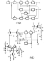
- reference numeral 1 illustrates a video processing stage which applies a video signal to a synchronizing signal separating stage 2.
- Stage 1 comprises a plurality of circuits in which an incoming video signal is amplified and processed in known manner.
- the signal from stage 1 comprises a composite synchronizing signal which is present at the output of stage 2 and is applied to a field synchronising signal separating stage 3and to a line synchronizing circuit.
- This circuit comprises a phase discriminator 4, a loop filter 5 and a line oscillator 6.
- Phase discriminator 4 determines the phase difference between the line synchronizing signal contained in the composite synchronizing signal and the line reference signal generated by oscillator 6 and in dependence on the phase difference measured a voltage is generated which is smoothed by filter 5.
- the smoothed voltage is applied to oscillator 6 for controlling the frequency and/or phase thereof.
- the reference signal has substantially the line frequency, i ⁇ e ⁇ the nominal frequency of the incoming line synchronizing pulses, namely 15.625 kHz for the European standard, and substantially the same phase as these pulses.
- the reference signal is applied to stages, not shown, in which it is further processed in known manner for the horizontal deflection in a picture display tube.
- Circuit 7 comprises, for example, a frequency dividing circuit to which the signal from line oscillator 6 is applied for dividing the frequency thereof, as a result of which in the nominal state of line phase control loop 4, 5, 6 a signal having the field frequency, i.e. 50 Hz for the European standard, is obtained, which is compared to the incoming field synchronizing signal.
- the field-frequency reference signal generated by circuit 7 has substantially the correct phase with respect to the field synchronizing signal and is applied to stages, not shown, for further processing for the vertical deflection in the picture display tube.
- Such a stage is, for example, a synchronizing detector with which coincidence between the incoming line synchronizing signal and the signal from oscillator 6 is determined for switching the elements of control loop 4, 5, 6 with the object of accelerating pull-in of the loop and also to increase the insensitivity to noise in the pulled-in state.
- a synchronizing detector with which coincidence between the incoming line synchronizing signal and the signal from oscillator 6 is determined for switching the elements of control loop 4, 5, 6 with the object of accelerating pull-in of the loop and also to increase the insensitivity to noise in the pulled-in state.
- the sensitivity of phase discriminator 4 and the time constant of Fig. 5 may then be given other vahes.
- the picture display device of which the above-mentioned stages form part also comprises a noise detector comprising an integrator 8, a noise separating stage 9, a counting device 10 and an output stage 11.
- the video signal present at the output of stage 1 is applied to integrator 8 which is in the form of a low-pass filter. By means thereof the high-frequency components are removed from the video signal.
- the signal obtained comprises few luminance and chrominance components, while the noise components are somewhat attenuated and the synchronizing pulses are substantially not influenced.
- the signal from line oscillator 6 is also applied to a pulse shaper 12 for producing a sampling pulse. This pulse occurs during a time interval located in the synchronized state of the line synchronizing circuit within the line synchronizing interval in the incoming video signal.
- the sampling pulse is free from noise and interference, and the edges thereof have a well- defined position in the time.
- the sampling pulse is applied to noise separating stage 9 for making this stage operative.
- the signal coming from integrator 8 is first differentiated and thereafter the signal obtained is amplified by stage 9 during the occurrence of the sampling pulse. Thanks to the described measures the amplified signal contains only noise components. This noise signal produces a pulse which is applied to counting device 10.
- Fig. 2 shows a possible embodiment of noise separating stage 9.
- the sampling pulse produced by pulse shaper 12 is applied to the base of an npn-transistor 22 via a kOhm resistor 21. Because of the action of the line phase control loop having elements 4, 5 and 6 it is ensured that an edge of the signal from oscillator 6 occurs approximately at the centre instant of a line synchronizing pulse synchronized therewith. By means of pulse shaper 12 a positively going pulse is produced which after the said edge has a duration of 1 to 195/us.
- the oscillator 6 may alternatively be in form of a sawtooth generator having a short flyback, pulse shaper 12 generating a pulse during the flyback period. The pulse from pulse-shaper 12 renders transistor 22 conductive.
- the emitter of transistor 22 is connected to ground via a 700 ⁇ resistor 23, while the collector is connected to the emitter of an npn transistor 24.
- the collector of transistor 24 is connected to the positive pole of a 12 V power supply whose negative pole is connected to ground.
- the emitter of a further npn transistor 25 is connected to the emitter of transistor 24 via a 2 kSL resistor 26.
- the collector of transistor 25 is connected to the base and to the collector of a pnp transistor 27 whose emitter is connected to the supply voltage.
- the base of transistor 25 is connected to a 14.7 k ⁇ resistor 28, whose other side is connected to the base of transistor 24, and to the junction between a 10 k ⁇ resistor 29, whose other side is connected to the supply voltage, and two diodes 30 and 31 arranged in series with the same forward directions.
- the anode of diode 30 is connected to the base of transistor 25 whereas the cathode of diode 31 is connected to ground.
- Integrator 8 comprises a 1 kSl series resistor and a parallel capacitor of 150 pF and affects the synchronizing pulses to a small extent.
- integrator 8 can be included in stage 1, that is to say integration can be effected before the output of this stage.
- the resultant slightly integrated video signal is a positive going signal, that is to say the synchronizing signal has a lower voltage level than the luminance signal. It is applied via a 2 k ⁇ resistor 32 to the base of an npn transistor 33, whose collector is connected to the supply voltage, whereas the emitter is connected to a 3.5 kSl resistor 34, whose other side is connected to ground.
- transistor 33 and resistor 34 constitute a separating stage between integrator 8 and stage 1, respectively and the differentiator formed by capacitor 35 and resistor 28.
- the base and the collector of transistor 27 are also connected to the base of a further pnp transistor 36 whose emitter is connected to the supply voltage, whereas the emitter is connected to a 10 k ⁇ resistor 37 and to the base of an npn transistor 38, whose emitter is connected to ground.
- the other side of resistor 37 is connected to a 7.5 kJ1 resistor 39 and to the collector of an npn transistor 40.
- the other terminal of resistor 39 and also the emitter of transistor 40 are connected to ground.
- Transistor 22 forms a current source which is only operative during the occurrence of the sampling pulse applied thereto.
- the emitter current of transistor 25 flows through resistor 26, which current, because of the high value of resistor 26 and the low value of the internal resistance of transistor 24 is predominantly determined by the high-frequency signal applied via capacitor 35.
- a current which has substantially the same value as the current through resistor 26 flows through resistor 37.
- transistor 40 is kept in the conducting state, in a way to be described still further, by the current through a 7.5 k ⁇ resistor 41 then it is clear that the noise signal present at the base of transistor 24 in the sampling interval is also present at the collector of transistor 36, but with a gain which is equal to the ratio between the values of resistors 37 and 26, that is to say 5 times in this example.
- a noise signal at the base of transistor 24 with an amplitude of at least approximately 120 mV consequently produces a signal of at least approximately 0.6 V at the base of transistor 38, which is sufficient to render this transistor conductive. Consequently, a pulse-shaped current flows through transistor 38. If the noise signal is less than approximately 120 mV then transistor 38 remains cut-off during the sampling interval.
- the current through transistor 38 produces at the collector a negatively-going voltage transient which is conveyed to counting device 10.
- This counting device comprises two counters 13 and 14 and a pulse generator 15.
- Generator 15 receives the control signal from field synchronizing circuit 7 and produces a window signal for counters 13 and 14.
- the window signal has a duration of 16 line periods and starts approximately 4 ms after the end of the field blanking interval, so it is located in the visible portion of the picture.
- counter 13 counts the number of times transistor 38 conducts and consequently the number of times stage 9 measures noise. If this number is equal to or greater than four then counter 13 stops counting causing a pulse to be applied to counter 14.
- Output stage 11 comprises a current mirror circuit including two pnp transistors 42 and 43 and is connected to counter 14. As soon as counter 14 has counted to two the level at its coutput becomes high so that no current flows through transistor 42 and consequently through transistor 43.
- the base of an npn transistor 44 is connected to the collector of transistor 43 and the collector is connected to the supply voltage, whereas a 7.5 k ⁇ resistor 45 and a 13.9 kll resistor 46 are arranged in series between the emitter and ground. In the described circumstances transistor 44 is in the non-conducting state. So the voltage at the emitter is zero.
- the junction of resistors 45 and 46 carries the output voltage of the noise detector. This junction is connected to phase discriminator 4 and filter 5 for changing their operation in known manner. Further portions of the picture display device can be changed. Then the change by means of the noise detector can be combined with a change controlled by the above-mentioned synchronization detector.
- the European Patent Application 59,379 describes such switcheable portions and also such a combination.
- the said junction is also connected to that terminal of resistor 41 which is not connected to the base of transistor 40.
- the last-mentioned measure has for its object to improve the operation of the noise detector somewhat, thanks to a hysteresis effect.
- stage 9 has a gain factor of 5. If the said condition has indeed been satisfied then transistor 40 is non-conducting, causing the value of the emitter-resistor of transistor 36 to be increased to 17.5 k4l and the gain factor of stage 9 to be increased to approximately 8.8. Thus, it is sufficient for stage 9 to measure a smaller quantity of noise to render transistor 38 conductive. This measure accomplishes that when noise is detected in a measuring period the noise detector has an increased sensitivity during the subsequent measuring period and thus it is easier for the detector to maintain the line synchronizing circuit in the state in which it has an improved immunity to noise.
- noise is measured in a short interval in which no video signal is present, it being a condition that the amplitude of the noise must exceed a predetermined threshold value to be taken into consideration, this threshold value being lower for the case in which the presence of noise was already determined previously. Since noise usually contains high-frequency components such components will certainly occur in the said interval.
- the number of times is counted in which noise was measured during a predetermined number of line periods, which line periods occur a certain time after the beginning of the field trace period, it being a condition that the counter exceeds a predetermined value.
- noise separating stage 9 is described as a keyed amplifier. It will be obvious that this stage may be replaced by a sample-and-hold circuit with the same function.
- Generator 15 is not described in detail as it may be of a known construction. If field synchronizing circuit 7 comprises a frequency dividing circuit for counting line periods then generator 15 can be of a simple construction for generating the window signal in that a certain number is counted for the leading edge and a second number for the trailing edge of this signal. Elements 13, 14 and 15 may be replaced by a microcomputer, whilst the place and the duration of the window signal, the maximum number of line periods and also the maximum number of field periods for the noise detection can be programmed optionally.
- Fig. 3 shows a possible embodiment of counters 13 and 14. These counters comprise flip-flops produced in accordance with the integrated injection logic (I 2 L) technique.
- Counter 13 comprises three flip-flops FF1, FF2 and FF3 which can be reset by the window signal via a transistor 51, whereas the set inputs S1, S 2 and S3 are connected to ground.
- the clock input CL 1 of flip-flop FF1 is connected to the collector of transistor 38, whereas the output Q 1 is connected to the clock input CL 2 of flip-flop FF2.
- the output Q 2 of flip-flop FF2 is connected to the clock input CL 3 of flip-flop FF3.
- the inserting output Q 1 of flip-flop FF1 is connected to the D-input D 1 of the same flip-flop and also to the inverting output Q 3 of flip-flop FF3.
- the inverting input Q 2 of flip-flop FF2 is connected to the D-input D 2 of the same flip-flop.
- the D-input D 3 of flip-flop FF3 carries a logic
- the reference symbols denote the logic signals at the similarly denoted terminals.
- the third impulse causes flip-flop FF1 to change state again, but Q 2 becomes zero at the fourth pulse only, when Q 1 becomes zero, in response to which Q 3 also becomes zero. As a result thereof also D 1 becomes zero. Subsequent clock pulses at input CL 1 will not have any influence on Q 3 , as Q 1 is and remains zero.
- Counter 14 comprises three flip-flops FF4, FF5 and FF6 of which both the set and the reset inputs S 4 , S 51 S 6 and R 4 , R 5 , R 69 respectively are connected to ground.
- the window signal is applied as a clock signal to flip-flops FF4 and FF5 via a transistor 52.
- the D-input D 4 of flip-flop FF4 is connected to the output Q 3 of flip-flop FF 3
- the D-input D 5 of flip-flop FF5 is connected to the output Q 4 of flip-flop FF4.
- the inverting outputs Q 4 and Q 5 of flip-flops FF4 and FF5, respectively are interconnected.
- Q 4 At the occurrence of the subsequent window signal, that is to say one field period later, Q 4 remains a logic 0 but Q 5 , which was a logic 1 becomes zero, causing both Q 4 and Q 5 to be 1. As long as Q 3 is zero subsequent clock pulses at inputs CL 4 and CL 5 will not have any influence on Q 5 . If Q 3 becomes a logic 1 after the occurrence of the first window signal, then Q 4 becomes an 1 at the occurrence of the second window signal, resulting in Q 4 and Q 5 becoming zero. This is the original state.
- the signal at output Q 5 when noise is measured, does not become a logic 1 until after two consecutive field periods.
- This information can be used as the output signal of the noise detector.
- a delay has been adopted for, more specifically by means of flip-flop FF6.
- a signal originating from circuit 7 is applied as a clock signal to this flip-flop via transistor 53, while the D-input D 6 is connected to the output Q 5 of flip-flop FF5.
- the output Q 6 of flip-flop FF6 is the output of counter 14 and is connected to the collector and to the base of transistor 42 via a transistor which operates as a current source.
Landscapes
- Engineering & Computer Science (AREA)
- Multimedia (AREA)
- Signal Processing (AREA)
- Synchronizing For Television (AREA)
- Picture Signal Circuits (AREA)
- Details Of Television Scanning (AREA)
Abstract
Description
- The invention relates to a picture display device comprising a video processing stage for supplying an incoming video signal containing at least a composite synchronizing signal, a synchronizing signal separating stage, connected to the video processing stage for supplying the composite synchronizing signal, a line synchronizing circuit coupled to the synchronizing signal separating stage for generating a line reference signal which is substantially synchronous with the line synchronizing signal present in the composite synchronizing signal, and a noise detector coupled to the video processing stage for detecting noise in the incoming video signal and for changing-over portions of the picture display device in dependence on the detected noise signal, this noise detector comprising a noise separating stage for differentiating the incoming video signal and for amplifying the resultant noise signal during the occurrence of a line signal, and also an output stage for supplying a change-signal derived from the amplified noise signal. Such a picture display device is disclosed in European Patent Application 59,379. In the television receiver described there a number of portions of the receiver are changed so as to improve the displayed picture when much noise is received. To that end the incoming video signal is delayed before it is applied to the synchronizing signal separating stage. The line synchronizing signal is generated with the aid of the delayed signal. During the occurrence of the line synchronizing signal the noise obtained by differentiation is amplified and thereafter the amplified noise signal is subjected to half-wave rectification. This results in a d.c. voltage. The value of this voltage depends on the quantity of noise contained in the video signal. When a predetermined value is exceeded this voltage provides the change. The differentiation of the video signal produces disturbing pulses during the occurrence of the edges of the non-delayed line synchronizing pulses. Thanks to the delay the disturbing pulse during the occurrence of the leading edge is removed, whereas the disturbing pulse caused by the trailing edge can be removed by half-wave rectification.
- If a great deal of noise is present than it may, happen that the synchronizing signal separating stage in the prior art arrangement is not capable of producing an adequate line signal for the noise separating stage. The weak line signal obtained may be shifted in the time relative to the incoming video signal, for example owing to reflections, so that no proper distinction can be made between the noise and the higher components of the video spectrum, i.e, luminance and, more specifically, chrominance components, with the result that the noise detector does not supply reliable information. A large-amplitude disturbing pulse occurring during the line trace period may also produce a signal for the noise separating stage.
- It is an object of the invention to provide a picture display device, of the above-described type, the time interval in which the noise separating stage is operative being determined in a reliable way. To this end the arrangement according to the invention is characterized in that connected to the noise separating stage there is a pulse shaper which is coupled to the line synchronizing circuit for generating a sampling pulse for making the noise separating stage operative during the occurrence of this pulse, this sampling pulse being derived from the line reference signal and in operation occurring during the line synchronizing period, the duration of the sampling pulse being shorter than the duration of the said period.
- The invention is based on the recognition that on reception of very much noise the line synchronizing circuit is also capable, thanks to the flywheel effect thereof, of producing a stable and reliable line reference signal and consequently a reliable sampling pulse, on the understanding that this pulse occurs each line period in an interval which is fixed in the time relative to the incoming video signal, in which interval this signal does not contain luminance and chrominance components.
- The distinction between noise and video signal components is further enhanced in that the arrangement according to the invention, is further characterized by an integrator for suppressing the high-frequency components of the incoming video signal applied to the noise separating stage.
- Advantageously, an arrangement comprising a field synchronizing signal connected to the synchronizing signal separating stage for deriving the field synchronizing signal present in the composite synchronizing signal obtained and connected to the field synchronizing signal separating stage a field synchronizing circuit for generating a field reference signal which is substantially synchronous with the incoming field synchronizing signal, is characterized in that the noise detector also comprises a counting device connected to the noise separating stage and to the field synchronizing circuit for counting the number of times the noise signal amplified by the noise separating stage exceeds a predetermined value and for causing a change-over signal to be generated by the output stage when the number of times counted during a predetermined number of line periods in the field trace period has reached a predetermined value. This measure is further based on the recognition that it is advantageous to have the presence of noise determined during a predetermined period of time. This results in a reliable criterion.
- The arrangement according to the invention may be characterized in that the counting device produces the change-over signal after the situation in which the said number found during the counting operation has reached the said predetermined value during a predetermined number of line periods in the field trace period repeats itself during a predetermined number of consecutive field periods.
- Improved operation of the noise detector is obtained if the arrangement is characterized in that the output stage is connected to the noise separating stage for increasing the gain factor thereof in the presence of the change-oer signal.
- The invention will now be described in greater detail by way of example with reference to the accompanying drawings. Herein
- Fig. 1 shows the block diagram of a portion of a picture display device, for example a television receiver, according to the invention and
- Figs. 2 and 3 show some details of the arrangement of Fig. 1,
- In Fig. 1
reference numeral 1 illustrates a video processing stage which applies a video signal to a synchronizing signal separating stage 2.Stage 1 comprises a plurality of circuits in which an incoming video signal is amplified and processed in known manner. The signal fromstage 1 comprises a composite synchronizing signal which is present at the output of stage 2 and is applied to a field synchronising signal separating stage 3and to a line synchronizing circuit. This circuit comprises a phase discriminator 4, aloop filter 5 and a line oscillator 6. Phase discriminator 4 determines the phase difference between the line synchronizing signal contained in the composite synchronizing signal and the line reference signal generated by oscillator 6 and in dependence on the phase difference measured a voltage is generated which is smoothed byfilter 5. The smoothed voltage is applied to oscillator 6 for controlling the frequency and/or phase thereof. In the final state of the phase control loop formed byelements 4, 5 and 6 the reference signal has substantially the line frequency, i·e· the nominal frequency of the incoming line synchronizing pulses, namely 15.625 kHz for the European standard, and substantially the same phase as these pulses. The reference signal is applied to stages, not shown, in which it is further processed in known manner for the horizontal deflection in a picture display tube. - At the mtput of the field synchronzing signal separating stage 3 the field synchronlzing signal present in the composite synchronizing signal is available for application to a
field synchronizing circuit 7.Circuit 7 comprises, for example, a frequency dividing circuit to which the signal from line oscillator 6 is applied for dividing the frequency thereof, as a result of which in the nominal state of linephase control loop 4, 5, 6 a signal having the field frequency, i.e. 50 Hz for the European standard, is obtained, which is compared to the incoming field synchronizing signal. The field-frequency reference signal generated bycircuit 7 has substantially the correct phase with respect to the field synchronizing signal and is applied to stages, not shown, for further processing for the vertical deflection in the picture display tube. - Everything described in the foregoing is of a known type. Other known stages may be present. Such a stage is, for example, a synchronizing detector with which coincidence between the incoming line synchronizing signal and the signal from oscillator 6 is determined for switching the elements of
control loop 4, 5, 6 with the object of accelerating pull-in of the loop and also to increase the insensitivity to noise in the pulled-in state. For this purpose the sensitivity of phase discriminator 4 and the time constant of Fig. 5 may then be given other vahes. - The picture display device of which the above-mentioned stages form part also comprises a noise detector comprising an
integrator 8, anoise separating stage 9, acounting device 10 and anoutput stage 11. The video signal present at the output ofstage 1 is applied tointegrator 8 which is in the form of a low-pass filter. By means thereof the high-frequency components are removed from the video signal. The signal obtained comprises few luminance and chrominance components, while the noise components are somewhat attenuated and the synchronizing pulses are substantially not influenced. The signal from line oscillator 6 is also applied to apulse shaper 12 for producing a sampling pulse. This pulse occurs during a time interval located in the synchronized state of the line synchronizing circuit within the line synchronizing interval in the incoming video signal. Contrary to the line synchronizing pulse, the sampling pulse is free from noise and interference, and the edges thereof have a well- defined position in the time. The sampling pulse is applied tonoise separating stage 9 for making this stage operative. The signal coming fromintegrator 8 is first differentiated and thereafter the signal obtained is amplified bystage 9 during the occurrence of the sampling pulse. Thanks to the described measures the amplified signal contains only noise components. This noise signal produces a pulse which is applied to countingdevice 10. - Fig. 2 shows a possible embodiment of
noise separating stage 9. The sampling pulse produced bypulse shaper 12 is applied to the base of an npn-transistor 22 via akOhm resistor 21. Because of the action of the line phase controlloop having elements 4, 5 and 6 it is ensured that an edge of the signal from oscillator 6 occurs approximately at the centre instant of a line synchronizing pulse synchronized therewith. By means of pulse shaper 12 a positively going pulse is produced which after the said edge has a duration of 1 to 195/us. The oscillator 6 may alternatively be in form of a sawtooth generator having a short flyback,pulse shaper 12 generating a pulse during the flyback period. The pulse from pulse-shaper 12renders transistor 22 conductive. The emitter oftransistor 22 is connected to ground via a700Ω resistor 23, while the collector is connected to the emitter of annpn transistor 24. The collector oftransistor 24 is connected to the positive pole of a 12 V power supply whose negative pole is connected to ground. The emitter of afurther npn transistor 25 is connected to the emitter oftransistor 24 via a 2kSL resistor 26. The collector oftransistor 25 is connected to the base and to the collector of apnp transistor 27 whose emitter is connected to the supply voltage. The base oftransistor 25 is connected to a 14.7kΩ resistor 28, whose other side is connected to the base oftransistor 24, and to the junction between a 10kΩ resistor 29, whose other side is connected to the supply voltage, and two diodes 30 and 31 arranged in series with the same forward directions. The anode of diode 30 is connected to the base oftransistor 25 whereas the cathode of diode 31 is connected to ground. -
Integrator 8 comprises a 1 kSl series resistor and a parallel capacitor of 150 pF and affects the synchronizing pulses to a small extent. Anthough different from Figure 1,integrator 8 can be included instage 1, that is to say integration can be effected before the output of this stage. The resultant slightly integrated video signal is a positive going signal, that is to say the synchronizing signal has a lower voltage level than the luminance signal. It is applied via a 2kΩ resistor 32 to the base of annpn transistor 33, whose collector is connected to the supply voltage, whereas the emitter is connected to a 3.5kSl resistor 34, whose other side is connected to ground. An 18pF capacitor 35 is arranged between the emitter oftransistor 33 and the base oftransistor 24. From this it can be seen thattransistor 33 andresistor 34 constitute a separating stage betweenintegrator 8 andstage 1, respectively and the differentiator formed bycapacitor 35 andresistor 28. - The base and the collector of
transistor 27 are also connected to the base of afurther pnp transistor 36 whose emitter is connected to the supply voltage, whereas the emitter is connected to a 10kΩ resistor 37 and to the base of annpn transistor 38, whose emitter is connected to ground. The other side ofresistor 37 is connected to a 7.5kJ1 resistor 39 and to the collector of an npn transistor 40. The other terminal ofresistor 39 and also the emitter of transistor 40 are connected to ground. -
Transistor 22 forms a current source which is only operative during the occurrence of the sampling pulse applied thereto. In the sampling interval the emitter current oftransistor 25 flows throughresistor 26, which current, because of the high value ofresistor 26 and the low value of the internal resistance oftransistor 24 is predominantly determined by the high-frequency signal applied viacapacitor 35. Because of the mirror inerting action by means oftransistors 27 and 36 a current which has substantially the same value as the current throughresistor 26 flows throughresistor 37. If transistor 40 is kept in the conducting state, in a way to be described still further, by the current through a 7.5 kΩ resistor 41 then it is clear that the noise signal present at the base oftransistor 24 in the sampling interval is also present at the collector oftransistor 36, but with a gain which is equal to the ratio between the values ofresistors transistor 24 with an amplitude of at least approximately 120 mV consequently produces a signal of at least approximately 0.6 V at the base oftransistor 38, which is sufficient to render this transistor conductive. Consequently, a pulse-shaped current flows throughtransistor 38. If the noise signal is less than approximately 120 mV thentransistor 38 remains cut-off during the sampling interval. - The current through
transistor 38 produces at the collector a negatively-going voltage transient which is conveyed to countingdevice 10. This counting device comprises twocounters pulse generator 15.Generator 15 receives the control signal fromfield synchronizing circuit 7 and produces a window signal forcounters times transistor 38 conducts and consequently the number of times stage 9 measures noise. If this number is equal to or greater than four then counter 13 stops counting causing a pulse to be applied to counter 14. The latter counter is enabled by the field signal fromcircuit 7 and subsequently counts to two consecutivefields Output stage 11 comprises a current mirror circuit including twopnp transistors counter 14 has counted to two the level at its coutput becomes high so that no current flows throughtransistor 42 and consequently throughtransistor 43. The base of annpn transistor 44 is connected to the collector oftransistor 43 and the collector is connected to the supply voltage, whereas a 7.5kΩ resistor 45 and a 13.9kll resistor 46 are arranged in series between the emitter and ground. In the describedcircumstances transistor 44 is in the non-conducting state. So the voltage at the emitter is zero. Ifcounter 13 has counted to less than four and/orcounter 14 has counted to less than two then, in contradistinction therewith, the level at the output ofcounter 14 is low, so thattransistors transistor 44 carries a positive voltage. - The junction of
resistors filter 5 for changing their operation in known manner. Further portions of the picture display device can be changed. Then the change by means of the noise detector can be combined with a change controlled by the above-mentioned synchronization detector. The European Patent Application 59,379 describes such switcheable portions and also such a combination. The said junction is also connected to that terminal of resistor 41 which is not connected to the base of transistor 40. The last-mentioned measure has for its object to improve the operation of the noise detector somewhat, thanks to a hysteresis effect. As long as the condition that counter 13 has counted to four andcounter 14 has counted to 2 has not been satisfied transistor 40 is conductive andstage 9 has a gain factor of 5. If the said condition has indeed been satisfied then transistor 40 is non-conducting, causing the value of the emitter-resistor oftransistor 36 to be increased to 17.5 k4l and the gain factor ofstage 9 to be increased to approximately 8.8. Thus, it is sufficient forstage 9 to measure a smaller quantity of noise to rendertransistor 38 conductive. This measure accomplishes that when noise is detected in a measuring period the noise detector has an increased sensitivity during the subsequent measuring period and thus it is easier for the detector to maintain the line synchronizing circuit in the state in which it has an improved immunity to noise. - From the foregoing it can be seen which standard is used for the decision that noise is indeed received. Firstly noise is measured in a short interval in which no video signal is present, it being a condition that the amplitude of the noise must exceed a predetermined threshold value to be taken into consideration, this threshold value being lower for the case in which the presence of noise was already determined previously. Since noise usually contains high-frequency components such components will certainly occur in the said interval. Secondly, the number of times is counted in which noise was measured during a predetermined number of line periods, which line periods occur a certain time after the beginning of the field trace period, it being a condition that the counter exceeds a predetermined value. The position in the field trace period in which these line periods are located is not critical, although the measurement must not be effected during the field blanking period. A reason therefor is that some types of video recording devices generate during the said period an encoding signal which might disturb the operation of the noise detector and of the line synchronizing circuit. Thirdly, the detected situation must repeat itself during a predetermined number of consecutive field periods. In the foregoing a description is given of the choices made in the described embodiment with respect to the amplitude of the noise, the duration of the window signal, the count of the line periods and the count of the field periods. It will be obvious that these choices were determined from actual practice and that other choices might have been made. It would, for example, be possible to emit counter 14 so that noise is only measured during one field period or to opt for a longer or shorter duration for the window signal.
- In the foregoing
noise separating stage 9 is described as a keyed amplifier. It will be obvious that this stage may be replaced by a sample-and-hold circuit with the same function.Generator 15 is not described in detail as it may be of a known construction. Iffield synchronizing circuit 7 comprises a frequency dividing circuit for counting line periods thengenerator 15 can be of a simple construction for generating the window signal in that a certain number is counted for the leading edge and a second number for the trailing edge of this signal.Elements - Fig. 3 shows a possible embodiment of
counters Counter 13 comprises three flip-flops FF1, FF2 and FF3 which can be reset by the window signal via atransistor 51, whereas the set inputs S1, S 2 and S3 are connected to ground. The clock input CL1 of flip-flop FF1 is connected to the collector oftransistor 38, whereas the output Q1 is connected to the clock input CL2 of flip-flop FF2. The output Q2 of flip-flop FF2 is connected to the clock input CL3 of flip-flop FF3. The inserting output Q1 of flip-flop FF1 is connected to the D-input D1 of the same flip-flop and also to the inverting output Q3 of flip-flop FF3. Similarly, the inverting input Q2 of flip-flop FF2 is connected to the D-input D2 of the same flip-flop. The D-input D3 of flip-flop FF3 carries a logic - The window signal accomplishes that Q1=Q2=0 and
Q 3= 1. Herein the reference symbols denote the logic signals at the similarly denoted terminals. Now D1= D2 = 1. If the collector oftransistor 38 becomes low, thenQ 1 = 1. At the subsequent pulse Q1 becomes zero, causing Q2 to become alogic 1. The third impulse causes flip-flop FF1 to change state again, but Q2 becomes zero at the fourth pulse only, when Q1 becomes zero, in response to which Q3 also becomes zero. As a result thereof also D1 becomes zero. Subsequent clock pulses at input CL1 will not have any influence on Q3, as Q1 is and remains zero. -
Counter 14 comprises three flip-flops FF4, FF5 and FF6 of which both the set and the reset inputs S4, S51 S6 and R4, R5, R69 respectively are connected to ground. The window signal is applied as a clock signal to flip-flops FF4 and FF5 via atransistor 52. The D-input D4 of flip-flop FF4 is connected to the outputQ 3 of flip-flop FF3, whereas the D-input D5 of flip-flop FF5 is connected to the output Q4 of flip-flop FF4. The inverting outputs Q4 and Q5 of flip-flops FF4 and FF5, respectively are interconnected. When the circuit is made operative flip-flops FF4 and FF5 keep counting until Q4 and Q5 have both become alogic 1. If counter 13 counts to less than four, then Q3 = D4 = 1, so that Q4 remains a 1 while flip-flop FF5 does not change state either. As long as Q3 remains a 1, this state is not changed at the occurrence of the subsequent window signals. If counter 13 counts, in contradistinction thereto, to four then Q3 = D4 = 0. At the occurrence of the window signal it is obtained that Q4 = D5 = 0, while Q5 does not change and consequently remains 1. Since Q5 is zero also Q4 is zero but this does not influence Q4. At the occurrence of the subsequent window signal, that is to say one field period later, Q4 remains a logic 0 but Q5, which was alogic 1 becomes zero, causing both Q4 and Q5 to be 1. As long as Q3 is zero subsequent clock pulses at inputs CL4 and CL5 will not have any influence onQ 5. If Q3 becomes alogic 1 after the occurrence of the first window signal, then Q4 becomes an 1 at the occurrence of the second window signal, resulting in Q4 and Q5 becoming zero. This is the original state. - From the foregoing it is to be seen that the signal at output Q 5, when noise is measured, does not become a
logic 1 until after two consecutive field periods. This information can be used as the output signal of the noise detector. In the embodiment of Fig. 3 a delay has been adopted for, more specifically by means of flip-flop FF6. A signal originating fromcircuit 7 is applied as a clock signal to this flip-flop viatransistor 53, while the D-input D6 is connected to the output Q 5 of flip-flop FF5. The output Q6 of flip-flop FF6 is the output ofcounter 14 and is connected to the collector and to the base oftransistor 42 via a transistor which operates as a current source. When no noise is measured the situation is maintained that D6 = Q5 = O and Q6 remains low, causingtransistor 42 to carry current. If the presence of noise is detected bystage 9 and flip-flops FF1 to FF5, in clu- sive then D6 becomes alogic 1. At the occurrence of the subsequent field signal at tclock input CL6, Q6 becomes high,causingtransistor 42 to be cut-off. In this way it is obtained that the change-over actions controlled by the noise detector are effected during a field change, that is to say at an instant at which no visible signal is displayed. This measure must be considered as a refinement. The same applies to the above-described hysteresis.
Claims (11)
Applications Claiming Priority (2)
| Application Number | Priority Date | Filing Date | Title |
|---|---|---|---|
| NL8302984A NL8302984A (en) | 1983-08-26 | 1983-08-26 | IMAGE DISPLAY WITH A NOISE DETECTOR. |
| NL8302984 | 1983-08-26 |
Publications (2)
| Publication Number | Publication Date |
|---|---|
| EP0135236A1 true EP0135236A1 (en) | 1985-03-27 |
| EP0135236B1 EP0135236B1 (en) | 1987-10-28 |
Family
ID=19842311
Family Applications (1)
| Application Number | Title | Priority Date | Filing Date |
|---|---|---|---|
| EP84201205A Expired EP0135236B1 (en) | 1983-08-26 | 1984-08-20 | Picture display device comprising a noise detector |
Country Status (7)
| Country | Link |
|---|---|
| US (1) | US4636860A (en) |
| EP (1) | EP0135236B1 (en) |
| JP (1) | JPS6069964A (en) |
| AU (1) | AU568398B2 (en) |
| DD (1) | DD222464A5 (en) |
| DE (1) | DE3467079D1 (en) |
| NL (1) | NL8302984A (en) |
Cited By (1)
| Publication number | Priority date | Publication date | Assignee | Title |
|---|---|---|---|---|
| WO1995024785A2 (en) * | 1994-03-07 | 1995-09-14 | Philips Electronics N.V. | Noise measurement |
Families Citing this family (8)
| Publication number | Priority date | Publication date | Assignee | Title |
|---|---|---|---|---|
| FR2625637B1 (en) * | 1988-01-04 | 1990-06-15 | Sgs Thomson Microelectronics | RECOGNITION CIRCUIT OF A MAGNETOSCOPE SIGNAL |
| JPH01204573A (en) * | 1988-02-10 | 1989-08-17 | Sony Corp | Noise reduction circuit |
| IT1229479B (en) * | 1989-03-13 | 1991-09-03 | Bioresearch Spa | USE OF 5 'DEOSSI 5' METHYLTHIOADENOSINE, S ADENOSYLMETHIONINE AND THEIR SALTS FOR THE PREPARATION OF PHARMACEUTICAL COMPOSITIONS SUITABLE TO PROMOTE THE GROWTH OF HAIR IN SUBJECTS AFFECTED BY Baldness and RELATIVE PHARMACEUTICAL COMPOSITIONS. |
| DE3924686A1 (en) * | 1989-07-26 | 1991-01-31 | Philips Patentverwaltung | SYNCHRONIZING ARRANGEMENT FOR AN IMAGE DISPLAY DEVICE |
| GB9113922D0 (en) * | 1991-06-27 | 1991-08-14 | Thomson Consumer Electronics | Television sync disable circuit |
| FR2742623B1 (en) * | 1995-12-18 | 1998-03-06 | Sgs Thomson Microelectronics | DEVICE FOR PROCESSING SYNCHRONIZATION SIGNALS |
| DE19743124B4 (en) * | 1997-09-30 | 2004-08-26 | Harman Becker Automotive Systems (Xsys Division) Gmbh | Method for determining the quality of a video signal and / or a television picture |
| CN113280912B (en) * | 2021-06-09 | 2024-03-05 | 湛江港(集团)股份有限公司 | Multi-dimensional noise monitoring system for industrial enterprise factory |
Citations (2)
| Publication number | Priority date | Publication date | Assignee | Title |
|---|---|---|---|---|
| US3806646A (en) * | 1972-09-11 | 1974-04-23 | Zenith Radio Corp | Noise processing system and method for use in a television receiver |
| EP0059379A2 (en) * | 1981-02-27 | 1982-09-08 | Sanyo Electric Co., Ltd. | Noise detecting circuit and television receiver employing the same |
Family Cites Families (6)
| Publication number | Priority date | Publication date | Assignee | Title |
|---|---|---|---|---|
| JPS5249730A (en) * | 1975-10-17 | 1977-04-21 | Matsushita Electric Ind Co Ltd | Noise detection unit |
| US4295161A (en) * | 1980-04-21 | 1981-10-13 | Rca Corporation | Keyed noise filter in a television receiver |
| JPS57142088A (en) * | 1981-02-27 | 1982-09-02 | Sanyo Electric Co Ltd | Detecting circuit for electric field strength |
| NL8103437A (en) * | 1981-07-21 | 1983-02-16 | Philips Nv | SYNCHRONIZER CIRCUIT FOR A TELEVISION RECEIVER. |
| US4376952A (en) * | 1981-07-30 | 1983-03-15 | Rca Corporation | Noise responsive automatic peaking control apparatus |
| JPS5831677A (en) * | 1981-08-19 | 1983-02-24 | Pioneer Electronic Corp | Video reproducer |
-
1983
- 1983-08-26 NL NL8302984A patent/NL8302984A/en not_active Application Discontinuation
-
1984
- 1984-08-09 US US06/639,164 patent/US4636860A/en not_active Expired - Fee Related
- 1984-08-20 DE DE8484201205T patent/DE3467079D1/en not_active Expired
- 1984-08-20 EP EP84201205A patent/EP0135236B1/en not_active Expired
- 1984-08-23 DD DD84266564A patent/DD222464A5/en not_active IP Right Cessation
- 1984-08-24 AU AU32377/84A patent/AU568398B2/en not_active Ceased
- 1984-08-24 JP JP59175342A patent/JPS6069964A/en active Granted
Patent Citations (2)
| Publication number | Priority date | Publication date | Assignee | Title |
|---|---|---|---|---|
| US3806646A (en) * | 1972-09-11 | 1974-04-23 | Zenith Radio Corp | Noise processing system and method for use in a television receiver |
| EP0059379A2 (en) * | 1981-02-27 | 1982-09-08 | Sanyo Electric Co., Ltd. | Noise detecting circuit and television receiver employing the same |
Cited By (2)
| Publication number | Priority date | Publication date | Assignee | Title |
|---|---|---|---|---|
| WO1995024785A2 (en) * | 1994-03-07 | 1995-09-14 | Philips Electronics N.V. | Noise measurement |
| WO1995024785A3 (en) * | 1994-03-07 | 1995-10-12 | Philips Electronics Nv | Noise measurement |
Also Published As
| Publication number | Publication date |
|---|---|
| AU568398B2 (en) | 1987-12-24 |
| JPH0342033B2 (en) | 1991-06-25 |
| AU3237784A (en) | 1985-02-28 |
| US4636860A (en) | 1987-01-13 |
| DE3467079D1 (en) | 1987-12-03 |
| JPS6069964A (en) | 1985-04-20 |
| EP0135236B1 (en) | 1987-10-28 |
| NL8302984A (en) | 1985-03-18 |
| DD222464A5 (en) | 1985-05-15 |
Similar Documents
| Publication | Publication Date | Title |
|---|---|---|
| EP0135236B1 (en) | Picture display device comprising a noise detector | |
| US4353091A (en) | Circuit for detecting faults in horizontal sync pulse signals | |
| EP0091719A1 (en) | Line synchronizing circuit for a picture display device and picture display device comprising such a circuit | |
| US6285403B1 (en) | Data slice circuit for slicing data carried on a video signal and a method thereof | |
| US4520393A (en) | Synchronizing circuit arrangement for deriving and processing a synchronizing signal contained in an incoming video signal | |
| EP0168089B1 (en) | Circuit for deriving a synchronizing signal contained in an incoming video signal | |
| US4496978A (en) | Noise detecting circuit and television receiver employing the same | |
| EP0281169B1 (en) | Line synchronising circuit in a picture display device | |
| US4415869A (en) | Sawtooth generator switchable between a free-running state or a synchronizable state | |
| KR930005185B1 (en) | Sync frequency automatic regulator | |
| US5963267A (en) | Delay correction circuit | |
| US5003391A (en) | Circuitry for processing a synchronizing signal | |
| US4388649A (en) | AFT Lockout prevention system | |
| EP0059379B1 (en) | Noise detecting circuit and television receiver employing the same | |
| US4446483A (en) | Circuit arrangement for deriving a field synchronizing signal from an incoming signal | |
| EP0406947B1 (en) | Synchronizing circuit including an oscillator | |
| US3743774A (en) | Synchronizing signal separation circuit | |
| US4789896A (en) | Vertical synchronizing pulse generating circuit | |
| EP0242907B1 (en) | Coincidence circuit in a line synchronizing circuit arrangement | |
| US3070657A (en) | Horizontal deflection synchronizing device | |
| US3717726A (en) | Noise immune color killer circuit | |
| US5251032A (en) | Line synchronizing circuit | |
| GB1583421A (en) | Secam television receiver | |
| JPS60248082A (en) | Circuit for detecting presence or absence of video signal reception | |
| US2605350A (en) | Synchronizing signal separator circuit |
Legal Events
| Date | Code | Title | Description |
|---|---|---|---|
| PUAI | Public reference made under article 153(3) epc to a published international application that has entered the european phase |
Free format text: ORIGINAL CODE: 0009012 |
|
| AK | Designated contracting states |
Designated state(s): DE FR GB IT NL |
|
| 17P | Request for examination filed |
Effective date: 19850919 |
|
| 17Q | First examination report despatched |
Effective date: 19860806 |
|
| GRAA | (expected) grant |
Free format text: ORIGINAL CODE: 0009210 |
|
| AK | Designated contracting states |
Kind code of ref document: B1 Designated state(s): DE FR GB IT NL |
|
| REF | Corresponds to: |
Ref document number: 3467079 Country of ref document: DE Date of ref document: 19871203 |
|
| ITF | It: translation for a ep patent filed | ||
| ET | Fr: translation filed | ||
| PLBE | No opposition filed within time limit |
Free format text: ORIGINAL CODE: 0009261 |
|
| STAA | Information on the status of an ep patent application or granted ep patent |
Free format text: STATUS: NO OPPOSITION FILED WITHIN TIME LIMIT |
|
| 26N | No opposition filed | ||
| PGFP | Annual fee paid to national office [announced via postgrant information from national office to epo] |
Ref country code: NL Payment date: 19900831 Year of fee payment: 7 |
|
| PG25 | Lapsed in a contracting state [announced via postgrant information from national office to epo] |
Ref country code: NL Effective date: 19920301 |
|
| NLV4 | Nl: lapsed or anulled due to non-payment of the annual fee | ||
| ITTA | It: last paid annual fee | ||
| ITPR | It: changes in ownership of a european patent |
Owner name: CAMBIO RAGIONE SOCIALE;PHILIPS ELECTRONICS N.V. |
|
| REG | Reference to a national code |
Ref country code: FR Ref legal event code: CD |
|
| PGFP | Annual fee paid to national office [announced via postgrant information from national office to epo] |
Ref country code: GB Payment date: 19960731 Year of fee payment: 13 |
|
| PGFP | Annual fee paid to national office [announced via postgrant information from national office to epo] |
Ref country code: FR Payment date: 19960828 Year of fee payment: 13 |
|
| PGFP | Annual fee paid to national office [announced via postgrant information from national office to epo] |
Ref country code: DE Payment date: 19961025 Year of fee payment: 13 |
|
| PG25 | Lapsed in a contracting state [announced via postgrant information from national office to epo] |
Ref country code: GB Free format text: LAPSE BECAUSE OF NON-PAYMENT OF DUE FEES Effective date: 19970820 |
|
| GBPC | Gb: european patent ceased through non-payment of renewal fee |
Effective date: 19970820 |
|
| PG25 | Lapsed in a contracting state [announced via postgrant information from national office to epo] |
Ref country code: FR Free format text: LAPSE BECAUSE OF NON-PAYMENT OF DUE FEES Effective date: 19980430 |
|
| PG25 | Lapsed in a contracting state [announced via postgrant information from national office to epo] |
Ref country code: DE Free format text: LAPSE BECAUSE OF NON-PAYMENT OF DUE FEES Effective date: 19980501 |
|
| REG | Reference to a national code |
Ref country code: FR Ref legal event code: ST |