DE19729163B4 - System and method for scan control of a programmable fuse circuit in an integrated circuit - Google Patents
System and method for scan control of a programmable fuse circuit in an integrated circuit Download PDFInfo
- Publication number
- DE19729163B4 DE19729163B4 DE19729163A DE19729163A DE19729163B4 DE 19729163 B4 DE19729163 B4 DE 19729163B4 DE 19729163 A DE19729163 A DE 19729163A DE 19729163 A DE19729163 A DE 19729163A DE 19729163 B4 DE19729163 B4 DE 19729163B4
- Authority
- DE
- Germany
- Prior art keywords
- fuse
- output
- latch
- scannable
- circuit
- Prior art date
- Legal status (The legal status is an assumption and is not a legal conclusion. Google has not performed a legal analysis and makes no representation as to the accuracy of the status listed.)
- Expired - Fee Related
Links
- 238000000034 method Methods 0.000 title description 15
- 230000001960 triggered effect Effects 0.000 claims abstract description 9
- 230000008859 change Effects 0.000 claims abstract description 3
- 238000005070 sampling Methods 0.000 claims description 8
- 238000013461 design Methods 0.000 claims description 6
- 238000012360 testing method Methods 0.000 description 20
- 230000002950 deficient Effects 0.000 description 14
- 230000007547 defect Effects 0.000 description 9
- 230000003213 activating effect Effects 0.000 description 7
- 238000013507 mapping Methods 0.000 description 6
- 230000008901 benefit Effects 0.000 description 5
- 239000002184 metal Substances 0.000 description 5
- 230000008439 repair process Effects 0.000 description 5
- 238000010586 diagram Methods 0.000 description 4
- 230000008569 process Effects 0.000 description 4
- 238000013100 final test Methods 0.000 description 3
- XUIMIQQOPSSXEZ-UHFFFAOYSA-N Silicon Chemical compound [Si] XUIMIQQOPSSXEZ-UHFFFAOYSA-N 0.000 description 2
- 230000007812 deficiency Effects 0.000 description 2
- 230000001419 dependent effect Effects 0.000 description 2
- 238000004519 manufacturing process Methods 0.000 description 2
- 229910021420 polycrystalline silicon Inorganic materials 0.000 description 2
- 229920005591 polysilicon Polymers 0.000 description 2
- 239000004065 semiconductor Substances 0.000 description 2
- 229910052710 silicon Inorganic materials 0.000 description 2
- 239000010703 silicon Substances 0.000 description 2
- 238000003860 storage Methods 0.000 description 2
- 230000003139 buffering effect Effects 0.000 description 1
- 238000010276 construction Methods 0.000 description 1
- 238000003745 diagnosis Methods 0.000 description 1
- 238000002405 diagnostic procedure Methods 0.000 description 1
- 230000000694 effects Effects 0.000 description 1
- 230000002996 emotional effect Effects 0.000 description 1
- 238000005538 encapsulation Methods 0.000 description 1
- 230000005669 field effect Effects 0.000 description 1
- 238000013508 migration Methods 0.000 description 1
- 230000005012 migration Effects 0.000 description 1
- 238000004806 packaging method and process Methods 0.000 description 1
- 238000002360 preparation method Methods 0.000 description 1
- 238000012545 processing Methods 0.000 description 1
- 238000013102 re-test Methods 0.000 description 1
- 230000008672 reprogramming Effects 0.000 description 1
- 230000029305 taxis Effects 0.000 description 1
- 238000012546 transfer Methods 0.000 description 1
- 230000007704 transition Effects 0.000 description 1
Classifications
-
- G—PHYSICS
- G11—INFORMATION STORAGE
- G11C—STATIC STORES
- G11C29/00—Checking stores for correct operation ; Subsequent repair; Testing stores during standby or offline operation
- G11C29/70—Masking faults in memories by using spares or by reconfiguring
- G11C29/78—Masking faults in memories by using spares or by reconfiguring using programmable devices
- G11C29/785—Masking faults in memories by using spares or by reconfiguring using programmable devices with redundancy programming schemes
- G11C29/789—Masking faults in memories by using spares or by reconfiguring using programmable devices with redundancy programming schemes using non-volatile cells or latches
-
- G—PHYSICS
- G01—MEASURING; TESTING
- G01R—MEASURING ELECTRIC VARIABLES; MEASURING MAGNETIC VARIABLES
- G01R31/00—Arrangements for testing electric properties; Arrangements for locating electric faults; Arrangements for electrical testing characterised by what is being tested not provided for elsewhere
- G01R31/28—Testing of electronic circuits, e.g. by signal tracer
- G01R31/317—Testing of digital circuits
- G01R31/3181—Functional testing
- G01R31/3185—Reconfiguring for testing, e.g. LSSD, partitioning
- G01R31/318533—Reconfiguring for testing, e.g. LSSD, partitioning using scanning techniques, e.g. LSSD, Boundary Scan, JTAG
-
- G—PHYSICS
- G11—INFORMATION STORAGE
- G11C—STATIC STORES
- G11C29/00—Checking stores for correct operation ; Subsequent repair; Testing stores during standby or offline operation
- G11C29/02—Detection or location of defective auxiliary circuits, e.g. defective refresh counters
-
- G—PHYSICS
- G11—INFORMATION STORAGE
- G11C—STATIC STORES
- G11C29/00—Checking stores for correct operation ; Subsequent repair; Testing stores during standby or offline operation
- G11C29/04—Detection or location of defective memory elements, e.g. cell constructio details, timing of test signals
- G11C29/08—Functional testing, e.g. testing during refresh, power-on self testing [POST] or distributed testing
- G11C29/12—Built-in arrangements for testing, e.g. built-in self testing [BIST] or interconnection details
- G11C29/18—Address generation devices; Devices for accessing memories, e.g. details of addressing circuits
- G11C29/30—Accessing single arrays
- G11C29/32—Serial access; Scan testing
Landscapes
- Engineering & Computer Science (AREA)
- General Engineering & Computer Science (AREA)
- Physics & Mathematics (AREA)
- General Physics & Mathematics (AREA)
- For Increasing The Reliability Of Semiconductor Memories (AREA)
- Tests Of Electronic Circuits (AREA)
- Test And Diagnosis Of Digital Computers (AREA)
- Design And Manufacture Of Integrated Circuits (AREA)
Abstract
Abtaststeuerbare,
programmierbare Sicherungsschaltung zur Verwendung in einer integrierten Schaltung
und mit einem Schaltungsausgang (A, B, C), mit folgenden Merkmalen:
einer
Sicherungsschaltung (11a, 11b, 11c) mit einem Sicherungsausgang
(16a, 16b, 16c), wobei die Sicherungsschaltung eine Sicherung (12a,
12b, 12c) aufweist, die ausgelöst werden
kann, um einen Logikpegel des Sicherungsausgangs zu ändern; und
einem
abtastbaren Latch (18a, 18b, 18c), das mit dem Sicherungsausgang
verbunden ist, und das zum Steuern des Schaltungsausgangs konfiguriert
ist, um es zu ermöglichen,
daß Ausgangswerte
in die abtastbare Latcheinrichtung von dem Sicherungsausgang geladen
werden, und dann zu dem Schaltungsausgang verschoben werden, und daß programmierte
Ausgangswerte in die abtastbare Latcheinrichtung hineingetastet
und dann zu dem Schaltungsausgang verschoben werden.Scannable programmable fuse circuit for use in an integrated circuit and having a circuit output (A, B, C), comprising:
a fuse circuit (11a, 11b, 11c) having a fuse output (16a, 16b, 16c), the fuse circuit having a fuse (12a, 12b, 12c) which can be triggered to change a logic level of the fuse output; and
a scannable latch (18a, 18b, 18c) connected to the fuse output and configured to control the circuit output to allow output values to be loaded into the scannable latch from the fuse output, and then shifted to the circuit output and programmed output values are keyed into the scannable latch and then shifted to the circuit output.
Description
Die vorliegende Erfindung bezieht sich auf eine programmierbare Sicherungsschaltungsanordnung und insbesondere auf das Steuern der Ausgabe einer programmierbaren Sicherungsschaltung mit einem abtastbaren Latch.The The present invention relates to a programmable fuse circuit arrangement and more particularly to controlling the output of a programmable Fuse circuit with a scannable latch.
Bei dem Entwurf von integrierten Schaltungen, die Speicher enthalten, wird eine gewisse Menge von Redundanz eingebaut, derart, daß Defekte, die während des Herstellens der integrierten Schaltung auftreten, durch Ersetzen des defekten Elements durch ein redundantes Element behoben werden können. Der Prozeß des Ersetzens des defekten Elements durch ein redundantes Element wird als "Kartographieren" bezeichnet, wobei das defekte Element "entkartographiert" wird, und das redundante Element "kartographiert" wird. Das Kartographieren wird typischerweise durch eine Sicherungslogikschaltungsanordnung durchgeführt, die durch eine oder mehrere programmierbare Sicherungsschaltungen gesteuert wird, die programmiert werden, um ein logisches Steuerungssignal an die Sicherungslogikschaltungsanordnung auszugeben. Eine programmierbare Sicherungsschaltung wird üblicherweise entweder durch Auslösen oder Nichtauslösen einer Sicherung programmiert, die der programmierbaren Sicherungsschaltung zugeordnet ist.at the design of integrated circuits containing memory, a certain amount of redundancy is built in, so that defects that while of manufacturing the integrated circuit by replacement of the defective element can be remedied by a redundant element can. The process of Replacing the defective element with a redundant element referred to as "mapping", wherein the defective element is "de-cartographed", and the redundant one Element is "mapped". The mapping is typically implemented by a back-up logic circuitry carried out, by one or more programmable fuse circuits which are programmed to provide a logic control signal to output to the backup logic circuitry. A programmable Fuse circuit is usually either by triggering or non-triggering programmed a fuse, the programmable fuse circuit assigned.
Beispielsweise ist eine Speicherbank, die eine Mehrzahl von Speicherelementen aufweist, eine übliche Struktur, die gut geeignet ist, um dieselbe redundant zu entwerfen, d. h. mit redundanten Speicherelementen. Wenn während des Herstellens eines der Speicherelemente in der Bank defekt wird, dann kann die Sicherungslogikschaltungsanordnung, die der Speicherbank zugeordnet ist, programmiert werden, um das defekte Element zu entkartographieren, und um ein redundantes Element zu kartographieren. Dementsprechend führen Hersteller von integrierten Schaltungen, um herauszufinden, welche Speicherelemente defekt sind, verschiedene Testtypen an verschiedenen Punkten während des Herstellungsprozesses durch. Von besonderer Relevanz ist dabei bezüglich der vorliegenden Erfindung ein Test, der als Scheibentest oder "Wafertest" bezeichnet wird.For example is a memory bank having a plurality of memory elements, a common one Structure that is well suited to redundantly designing it d. H. with redundant memory elements. If during the making of a the memory elements in the bank becomes defective, then the backup logic circuitry, the the memory bank is assigned to be programmed to the defective element to de-cartograph and to map a redundant element. Accordingly lead Manufacturer of integrated circuits to find out which storage elements are defective, different test types at different points during the Through the manufacturing process. Of particular relevance is in terms of present invention, a test which is referred to as a disk test or "wafer test".
Im allgemeinen ist das Scheibentesten ein Mittel zum Verifizieren der korrekten Operation einer integrierten Schaltung, sobald dieselbe hergestellt ist, und sich in einer Scheibenform befindet.in the In general, disk testing is a means of verifying the correct operation of an integrated circuit as soon as it is the same is made, and is in a disk shape.
Folglich werden, sobald die integrierte Schaltung hergestellt wurde, jedoch bevor die Scheibe in einzelne Chips geschnitten wird, Scheibentests an der integrierten Schaltung durchgeführt, um zu bestimmen, ob der Speicher ordnungsgemäß arbeitet, oder ob sich defekte Speicherelemente in derselben befinden. Wenn defekte Speicherelemente geortet werden, dann wird die Scheibe von dem Scheibentester entfernt, und dieselbe wird zu einer Laserprogrammierstation genommen, bei der die programmierbaren Sicherungsschaltungen programmiert werden, um die Sicherungslogikschaltungsanordnung mit einer geeigneten Logikstruktur zum Kartographieren der Speicherbank zu versehen. Die programmierbaren Sicherungsschaltungen werden bei der Laserprogrammierstation durch einen Laser programmiert, der die Sicherungen "auslöst", die den ausgewählten programmierbaren Sicherungsschaltungen zugeordnet sind. Es gibt derzeit keine verfügbare Einrichtung zum Verifizieren, ob das Laserprogrammieren erfolgreich ist, ohne einen zweiten Scheibentest durchführen zu müssen. Die Scheibe wird daher zu dem Scheibentester zum erneuten Testen der integrierten Schaltung zurückgebracht, um zu bestätigen, daß das Laserprogrammieren den Defekt vor dem Endaufbau der integrierten Schaltung repariert hat. Der vorhergehende Prozeß ist nicht nur kostenintensiv und zeitaufwendig, derselbe erfordert jedoch ferner, daß die integrierte Schaltung zweimal scheibengetestet wird, wodurch die Wahrscheinlichkeit erhöht wird, daß die integrierte Schaltung weiter beschädigt wird, jedesmal, wenn die integrierte Schaltung gehandhabt oder getestet wird.consequently however, once the integrated circuit has been manufactured before the disk is cut into individual chips, disk tests performed on the integrated circuit to determine if the Memory is working properly, or whether there are defective memory elements in the same. If broken Storage elements are located, then the disc is from the disk tester removed and the same is taken to a laser programming station, in which the programmable fuse circuits are programmed, the fuse logic circuitry with a suitable logic structure to map the memory bank. The programmable Fuse circuits are performed at the laser programming station programmed a laser that "triggers" the fuses that make up the selected programmable Assigned to fuse circuits. There is currently no available facility to verify that laser programming is successful without to perform a second disk test. The disc is therefore to the disk tester for re-testing the integrated circuit brought back, to confirm, that this Laser programming the defect before the final construction of the integrated Has repaired circuit. The previous process is not only costly and time consuming, but it also requires that the integrated Circuit is twice disc-tested, reducing the probability elevated will that the integrated circuit continues to be damaged every time the integrated circuit is handled or tested.
Weiterhin sind Speicherbänke oftmals ein Teil einer eingebetteten Speicherschaltung, wobei andere Schaltungsanordnungen in der integrierten Schaltung den eingebetteten Speicher verwenden (d. h. von demselben abhängen). Der Speicher muß folglich vollständig funktionsfähig und in seinem Endzustand konfiguriert sein, um ein vollständiges Testen der anderen Nicht-Speicherschaltungen zu ermöglichen. Wenn der Betrieb des Speichers nicht vollständig bei dem ersten Scheibentest konfiguriert wird, dann können die anderen Schaltungen, die den Speicher verwenden, nicht vollständig getestet werden, bis der Speicher kartographiert und der zweite Scheibentest durchgeführt wurde, um die Reparatur zu bestätigen. Dies ist wiederum kostenintensiv und zeitaufwendig.Farther are memory banks often part of an embedded memory circuit, with others Circuits in the integrated circuit embedded Use memory (that is, depend on it). The memory must therefore Completely functioning and be configured in its final state for complete testing to enable the other non-memory circuits. When the operation of the Memory not complete is configured at the first disk test, then the other circuits that use the memory are not fully tested until the memory is mapped and the second disk test carried out was to confirm the repair. This again is costly and time consuming.
Eine weitere Option besteht darin, den Speicher und die Nicht-Speicherschaltungen unabhängig bei dem Scheibentest zu testen, die redundanten Elemente des Speichers zu konfigurieren und dann den Endaufbau in einer Gehäuseform oder "gepackaged" zu testen. Dies hinterläßt jedoch die Schnittstelle zwischen dem Speicher und den Nicht-Speicherschaltungen ungetestet, und daher können Defekte existieren, die bewirken, daß die integrierte Schaltung bei dem Endtesten versagt. Die Kosten des Aufbaus und des Häusens der integrierten Schaltung gehen, wenn die integrierte Schaltung beim Endtest versagt, sonst verloren. Ein weiterer Nachteil dieser Option besteht darin, daß die Nicht-Speicherschaltungen nicht testbar sind, ohne daß der Speicher konfiguriert ist. Dies kann einen zusätzlichen Ausbeuteverlust beim Endtesten bewirken.Another option is to independently test the memory and non-memory circuits in the disk test, configure the redundant elements of the memory, and then test the final assembly in a package form or "packaged". However, this leaves the interface between the memory and the non-memory circuits untested, and therefore defects may exist which cause the integrated circuit to fail in the final test. The cost of building and packaging the integrated circuit will otherwise be lost if the integrated circuit fails the final test. Another disadvantage this option is that the non-memory circuits are not testable without the memory being configured. This can cause an additional yield loss in final testing.
Sobald eine integrierte Schaltung gehäust und in Betrieb genommen wird, können zusätzlich gewisse physikalische Phänomene und/oder Aktivitäten zu latenten Defekten beitragen.As soon as an integrated circuit housed and can be put into operation in addition certain physical phenomena and / or activities contribute to latent defects.
Wenn derartige Defekte auftreten, wird die integrierte Schaltung typischerweise als irreparabel betrachtet, und daher muß die integrierte Schaltung (oder das Produkt, in dem dieselbe gehäust ist) ersetzt werden. Derzeit ist keine Einrichtung zum Neuprogrammieren der programmierbaren Sicherungsschaltungen, die die Sicherungslogikschaltungsanordnung steuern, verfügbar, um diese latenten Defekte zu überwinden.If If such defects occur, the integrated circuit typically becomes considered irreparable, and therefore the integrated circuit (or the product in which it is housed is) replaced. There is currently no facility for reprogramming the programmable fuse circuits, the fuse logic circuitry control, available, to overcome these latent defects.
Die
Die
Die Aufgabe der vorliegenden Erfindung besteht darin, eine programmierbare Sicherungsschaltung zu schaffen, die ohne die programmierbare Sicherungsschaltung permanent programmieren zu müssen, neu programmiert werden kann.The Object of the present invention is a programmable To provide a fuse circuit without the programmable fuse circuit to have to program permanently can be reprogrammed.
Diese Aufgabe wird durch eine Sicherungsschaltung gemäß Anspruch 1 gelöst.These The object is achieved by a fuse circuit according to claim 1.
Die vorliegende Erfindung überwindet die Unzulänglichkeiten und Mängel des Stands der Technik, wie im vorhergehenden beschrieben, und wie in der Industrie bekannt. Die vorliegende Erfindung schafft ein abtastbares Latch, das in einer programmierbaren Sicherungsschaltung verwendet werden kann, um eine Abtaststeuerung der Ausgabe der programmierbaren Sicherungsschaltung zu schaffen. Im wesentlichen ermöglicht das abtastbare Latch, daß die tatsächliche Ausgabe der programmierbaren Sicherungsschaltung geladen werden kann, und zu dem Ausgang des abtastbaren Latchs verschoben werden kann, an dem der Ausgangswert der programmierbaren Sicherungsschaltung gelesen werden kann, oder alternativ, daß ein programmierter Ausgangswert hineinabgetastet werden kann, und zu dem Ausgang des abtastbaren Latchs, an dem der programmierte Wert gelesen werden kann, verschoben werden kann. Dies liefert die Funktionalität, um jede Nicht-Speicherschaltungsanordnung testen zu können, die davon abhängt, daß der Speicher voll funktionsfähig und betriebsfähig ist, während sich dieselbe noch bei dem Scheibentester befindet, bevor jegliche Sicherungen bei der Laserprogrammierstation ausgelöst werden. Zusätzlich liefern die abtastbaren Latchs die Funktionalität, um das Programmieren der Sicherungen durch Laden der Ausgangssignale der programmierbaren Sicherungsschaltungen, nachdem die ausgewählten Sicherungen ausgelöst wurden, und durch Abtasten derselben verifizieren zu können.The overcomes the present invention the shortcomings and defects of the prior art as described above, and how known in the industry. The present invention provides Scannable latch in a programmable fuse circuit can be used to control the output of programmable sampling control To provide security circuit. In essence, this allows scannable latch that the actual Output of the programmable fuse circuit are loaded can be moved to the output of the scannable latch may be at which the output value of the programmable fuse circuit can be read, or alternatively, that a programmed output value can be scanned in, and to the output of the scannable Latches, where the programmed value can be read, moved can be. This provides the functionality to any non-memory circuitry to be able to test which depends that the Memory fully functional and operational is while the same is still at the disk tester before any Fuses are triggered at the laser programming station. additionally The scannable latches provide the functionality to program the Fuses by loading the programmable output signals Backup circuits after the selected fuses have been triggered, and be able to verify by scanning them.
Daher und gemäß der Erfindung ist der Ausgang der programmierbaren Sicherungsschaltung mit dem Eingang eines abtastbaren Latchs verbunden, derart, daß das abtastbare Latch den Ausgangswert der programmierbaren Sicherungsschaltung laden kann, und dann den Ausgangswert auf den Ausgang des abtastbaren Latchs schaltet. Alternativ dazu kann das abtastbare Latch einen Ausgangswert hineinabtasten, und den abgetasteten Wert zu dem Ausgang des abtastbaren Latchs verschieben. Bei einer bevorzugten Konfiguration wird die vorhergehende Funktionalität durch ein abtastbares Latch erreicht, das in einem Drei-Latch-Entwurf implementiert ist, der ein Datenlatch, ein Schieberegistermasterlatch und ein Schieberegisterslavelatch aufweist. Das Datenlatch umfaßt ein einzelnes Latch, mit zwei Eingangssignalen (LADEN oder "LOAD" und SCHREIBEN oder "WRITE"), die von dem Eingang des abtastbaren Latchs oder von dem Schieberegisterslavelatch geladen werden können. Das Schieberegistermasterlatch und ein Schieberegisterslavelatch sind seriell verbunden, um ein Master-Slave-Schieberegister mit zwei Eingangssignalen (HINEINABTASTEN oder "SCANIN" und LESEN oder "READ") zum Steuern der Operationen des "Hineinabtastens" von Daten und des "Hinausabtastens" von Daten zu steuern. Es sei jedoch bemerkt, daß jegliche Implementation eines geeigneten abtastbaren Latchs in der vorliegenden Erfindung enthalten sein kann, und daß diese verschiedenen Implementationen lediglich eine Entwurfswahl sind. Bei dem bevorzugten Ausführungsbeispiel sind eine Mehrzahl von abtastbaren Latchs als Parallel-Hinein-, Parallel-Hinaus-Schieberegister verbunden, wie es in der Technik bekannt ist. Jedem Eingang des Schieberegisters ist eine programmierbare Sicherungsschaltung, wie die im folgenden beschriebene Schaltung, zugeordnet.Therefore, and in accordance with the invention, the output of the programmable fuse circuit is connected to the input of a scannable latch such that the scannable latch can load the output value of the programmable fuse circuit and then switch the output value to the output of the scannable latch. Alternatively, the scannable latch may sample in an output value and shift the sampled value to the output of the scannable latch. In a preferred configuration, the foregoing functionality is achieved by a scannable latch implemented in a three-latch design comprising a data latch, a shift register master latch, and a shift register latch latch. The data latch comprises a single latch, with two input signals (LOAD or "LOAD" and WRITE or "WRITE") which can be loaded from the input of the scannable latch or from the shift register latch latch. The shift register master latch and a shift register slave latch are connected in series to provide a master-slave shift register with two input signals (HI-INBUT or "SCANIN" and READ or "READ") for controlling the operations of "scanning in" data and "oversampling" data Taxes. It should be understood, however, that any implementation of an appropriate scannable latch in the present invention and that these various implementations are merely a design choice. In the preferred embodiment, a plurality of scannable latches are connected as parallel in, parallel out of shift registers, as is known in the art. Each input of the shift register is associated with a programmable fuse circuit, such as the circuit described below.
Die programmierbare Sicherungsschaltung, mit der das abtastbare Latch verbunden ist, kann viele Formen annehmen. Zum Zweck der Offenbarung der vorliegenden Erfindung ist hierin jedoch ein bevorzugtes Ausführungsbeispiel beschrieben, obwohl klar sein sollte, daß die Prinzipien der vorliegenden Erfindung praktisch auf jede programmierbare Sicherungsschaltungskonfiguration gleich anwendbar sind. Bei dem bevorzugten Ausführungsbeispiel, das hierin offenbart ist, weist die programmierbare Sicherungsschaltung ein Lastbauelement und eine Sicherung auf, die seriell miteinander verbunden sind. Das Lastbauelement ist mit der Spannungsversorgung (VDD) verbunden, und die Sicherung ist mit der Erde (ERDE) verbunden. Der Sicherung ist ein Ausgangssignal zugeordnet, das an der Verbindung zwischen dem Lastbauelement und der Sicherung abgenommen wird. Das Lastbauelement ist vorzugsweise ein NWELL-Widerstand (NWELL = N-WANNE) oder ein PMOS-FET, obwohl jedes resistive Bauelement verwendet werden kann. Zusätzlich ist die Sicherung vorzugsweise eine Metallschicht, die entweder leitfähig oder nicht leitfähig ist, abhängig davon, ob dieselbe während des Programmierens ausgelöst wurde. Alternativ kann anstelle der Metallschicht eine Polysilizium- oder Siliziumschicht verwendet werden.The programmable fuse circuit, with which the scannable latch can take many forms. For the purpose of disclosing the However, the present invention is a preferred embodiment herein although it should be understood that the principles of the present invention virtually any programmable fuse circuit configuration are equally applicable. In the preferred embodiment, herein discloses the programmable fuse circuit Load component and a fuse connected in series are. The load device is connected to the power supply (VDD), and the fuse is connected to earth (EARTH). The fuse is associated with an output signal connected to the connection between the Load component and the fuse is removed. The load component is preferably a NWELL resistor (NWELL = N-TANK) or a PMOS-FET, although any resistive device can be used. In addition is the fuse is preferably a metal layer which is either conductive or not conductive depends on of whether the same during of programming has been. Alternatively, instead of the metal layer, a polysilicon or silicon layer can be used.
Die vorliegende Erfindung stellt nicht nur ein System zur Abtaststeuerung von programmierbaren Sicherungsschaltungen sondern ferner verschiedene Methoden für die Abtaststeuerung von programmierbaren Sicherungen bereit. Ein erstes Verfahren zum Verifizieren des Programmierens der programmierbaren Sicherungsschaltung kann in die folgenden Schritte verallgemeinert werden: Verbinden eines abtastbaren Latchs mit der programmierbare Sicherungsschaltung, derart, daß der Ausgang der Sicherungsschaltung mit dem Eingang des abtastbaren Latchs verbunden ist; Zwischenspeichern der programmierten Sicherungsdaten von der programmierbaren Sicherungsschaltung in dem abtastbaren Latch; und Herausabtasten der programmierten Sicherungsdatenwerte der programmierbaren Sicherungsschaltung, um das Programmieren der programmierbaren Sicherungsschaltung zu verifizieren. Ein zweites Verfahren zum Testen von Nicht-Speicherschaltungen, abhängig von dem Speicher, der der programmierbaren Sicherungsschaltung zugeordnet ist, kann durch die folgenden Schritte verallgemeinert werden: Verbinden eines abtastbaren Latchs mit einer programmierbaren Sicherungsschaltung, derart, daß der Ausgang der Sicherungsschaltung mit dem Eingang des abtastbaren Latchs verbunden ist; Abtasten eines Ausgangsdatenwerts in das abtastbare Latch; und Verschieben des Ausgangsdatenwerts zu dem Ausgang des abtastbaren Latchs, um die Nicht-Speicherschaltungen abhängig von dem Speicher, der den Sicherungsschaltungen zugeordnet ist, zu testen. Dieses zweite Verfahren ermöglicht ferner das Verifizieren der vorgeschlagenen Programmierung der programmierbaren Sicherungsschaltung, wie es durch den Ausgangsdatenwert dargestellt wird.The The present invention not only provides a system for scan control of programmable fuse circuits but also different methods for the Scan control of programmable fuses ready. A first Method for verifying the programming of the programmable Fuse circuit can be generalized in the following steps Connect a scannable latch to the programmable latch Fuse circuit, such that the Output of the fuse circuit with the input of the scannable latch connected is; Caching the programmed backup data from the programmable fuse circuit in the scannable latch; and sampling out the programmed fuse data values of the programmable Fuse circuit to program the programmable fuse circuit to verify. A second method for testing non-memory circuits, dependent from the memory associated with the programmable fuse circuit can be generalized by the following steps: connect a scannable latch with a programmable fuse circuit, such that the Output of the fuse circuit with the input of the scannable Latches connected; Scanning an output data value into the scannable one latch; and shifting the output data value to the output of the scannable latches to the non-memory circuits depending on the Memory to be assigned to the fuse circuits. This second method allows further verifying the proposed programming of the programmable Fuse circuit as represented by the output data value becomes.
Zusätzlich zu den obigen Merkmalen weisen das System und das Verfahren der vorliegenden Erfindung viele Vorteile auf, von denen ein paar im folgenden als Beispiele beschrieben sind.In addition to The above features indicate the system and method of the present invention Invention has many advantages, a few of which below Examples are described.
Ein Vorteil der vorliegenden Erfindung besteht darin, daß dieselbe die Redundanz ermöglicht, daß ein Speicherblock in eine Endkonfiguration bei dem Scheibentester programmiert wird, derart, daß die Schaltungsanordnung, die von der Speicherbank abhängig ist, vollständig vor dem Endprogrammieren der Sicherungen bei einer Laserprogrammierstation getestet werden kann.One Advantage of the present invention is that the same the redundancy allows a memory block programmed into a final configuration at the disk tester, such that the Circuitry dependent on the memory bank Completely tested before final programming of the fuses at a laser programming station can be.
Ein weiterer Vorteil der vorliegenden Erfindung besteht darin, daß dieselbe ein Verifizieren der Laserprogrammierung einer programmierbaren Sicherungsschaltung durch Herausabtasten der programmierten Sicherungswerte vorsieht.One Another advantage of the present invention is that the same verifying the laser programming of a programmable Fuse circuit by sampling out the programmed fuse values provides.
Noch ein weiterer Vorteil der vorliegenden Erfindung besteht darin, daß die Redundanz bei einer integrierten Schaltung über das abtastbare Latch zu jeder Zeit neu programmiert werden kann, sogar durch Aufheben der Laserprogrammierung.Yet Another advantage of the present invention is that the redundancy with an integrated circuit via the scannable latch to each Time can be reprogrammed, even by reversing the laser programming.
Bevorzugte Ausführungsbeispiele der vorliegenden Erfindung werden nachfolgend unter Bezugnahme auf die beiliegenden Zeichnungen näher erläutert. Es zeigen:preferred embodiments The present invention will be described below with reference to FIG the enclosed drawings closer explained. Show it:
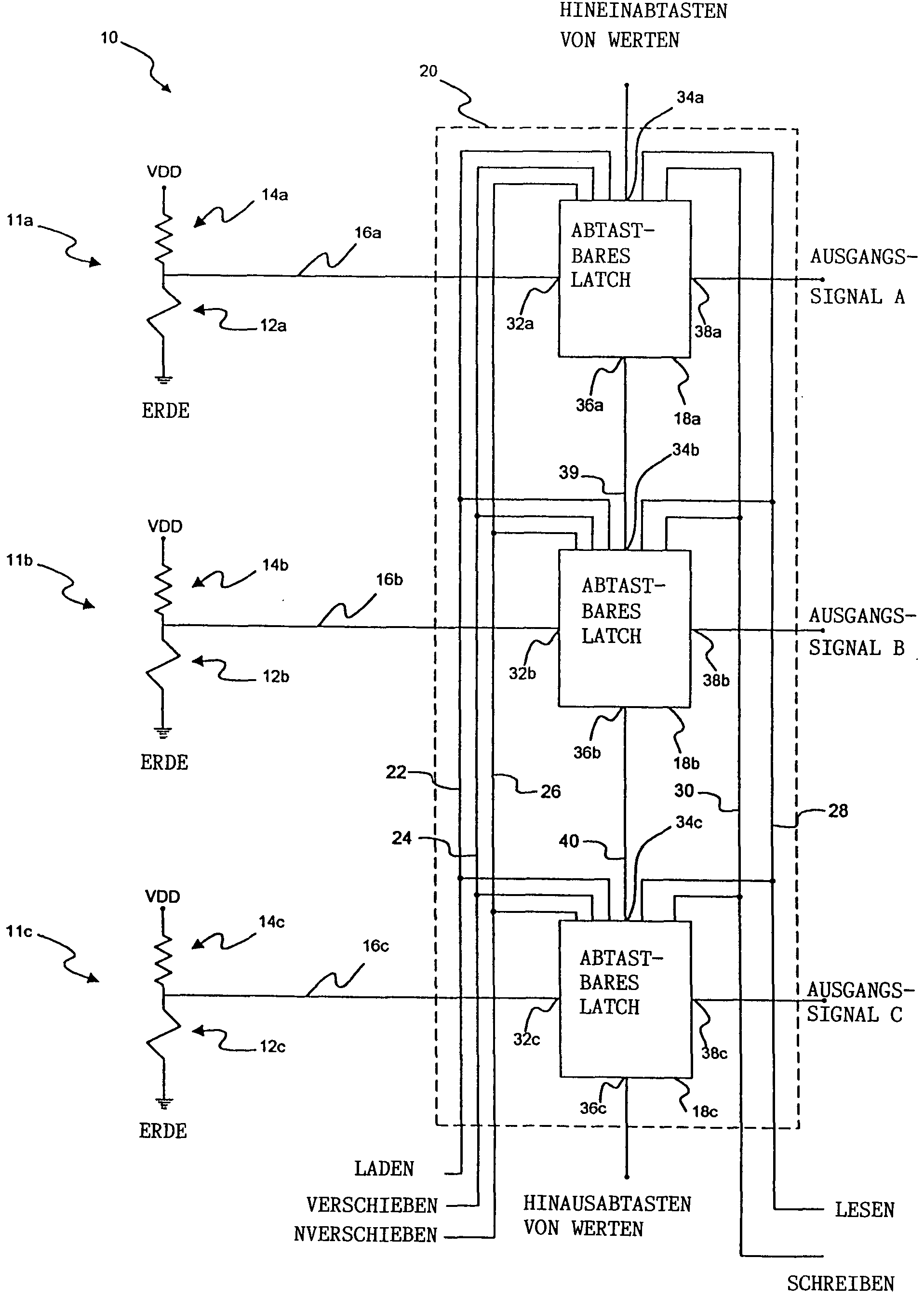
I. ArchitekturI. Architecture
Unter
Bezugnahme auf die Zeichnungen, zeigt die
Die
abtaststeuerbare, programmierbare Sicherungsschaltung
Bei
einem bevorzugten Ausführungsbeispiel weisen
die Sicherungen
Mit
der Ausgangsleitung
Die
LADEN-Leitung
Es
sei ferner angemerkt, daß das
HINAUSABTASTEN-Tor
Nimmt
man nun Bezug auf
Das
abtastbare Latch
Das
Datenlatch
Das
Schieberegistermasterlatch
Das
Schieberegisterslavelatch
II. BetriebII. Operation
Eine
besondere Funktionalität,
die der abtaststeuerbaren, programmierbaren Sicherungsschaltung
Beim
Betrieb kann, sobald ein defektes Speicherelement über das
Scheibentesten lokalisiert wurde, eine spezielle Ausgangsdatenstruktur
für die
abtaststeuerbare, programmierbare Sicherungsschaltung 10 zum Kartographieren
der Speicherbank bestimmt werden, um das defekte Speicherelement durch
ein redundantes Speicherelement über
die Sicherungslogikschaltungsanordnung zu ersetzen. Früher konnte
diese Ausgangsdatenstruktur lediglich durch Auslösen der geeigneten Sicherungen
Dementsprechend
enthält
die abtaststeuerbare, programmierbare Sicherungsschaltung
Unter
Bezugnahme auf
Unter
Bezugnahme auf
Ein
Zeitablaufdiagramm
Zum
Zweck des Lesezyklus
Wenn
der Lesen-Schalter
Eine
Datenstruktur kann ferner seriell durch das abtastbare Latch
Zum
Zweck des Schreibzyklusses
Zunächst befindet
sich der erste Datenwert, der hinein abgetastet wird, bei einem
hohen Wert, und daher befindet sich das Signal an dem HINEINABTASTEN-Tor
Der
dritte Datenwert, der hineinabzutasten ist, ist ein weiterer niedriger
Wert, und daher verbleibt das Signal an dem HINEINABTASTEN-Tor
Das
Schieberegisterslavelatch
Die
Ausgangssignalstrukturen der abtaststeuerbaren, programmierbaren
Sicherungsschaltung
Wenn
die programmierte Ausgangsstruktur anscheinend den Speicher erfolgreich
neu kartographiert, kann die Scheibe zu einem Laserprogrammierer
(oder jedem anderen sicherungsauslösenden System) gebracht werden,
bei dem die geeigneten Sicherungen
Eine
weitere Funktionalität,
die durch die vorliegende Erfindung bereitgestellt wird, besteht
darin, daß dieselbe
eine weiche Programmier- oder temporäre Programmierfähigkeit
bezüglich
des Speichers vorsieht. Dies ermöglicht
es der abtaststeuerbaren, programmierbaren Sicherungsschaltung
Claims (7)
Applications Claiming Priority (2)
| Application Number | Priority Date | Filing Date | Title |
|---|---|---|---|
| US08/692,736 US5668818A (en) | 1996-08-06 | 1996-08-06 | System and method for scan control of a programmable fuse circuit in an integrated circuit |
| US08/692,736 | 1996-08-06 |
Publications (2)
| Publication Number | Publication Date |
|---|---|
| DE19729163A1 DE19729163A1 (en) | 1998-02-12 |
| DE19729163B4 true DE19729163B4 (en) | 2006-03-02 |
Family
ID=24781800
Family Applications (1)
| Application Number | Title | Priority Date | Filing Date |
|---|---|---|---|
| DE19729163A Expired - Fee Related DE19729163B4 (en) | 1996-08-06 | 1997-07-08 | System and method for scan control of a programmable fuse circuit in an integrated circuit |
Country Status (4)
| Country | Link |
|---|---|
| US (1) | US5668818A (en) |
| JP (1) | JPH1092291A (en) |
| DE (1) | DE19729163B4 (en) |
| GB (1) | GB2316180B (en) |
Families Citing this family (32)
| Publication number | Priority date | Publication date | Assignee | Title |
|---|---|---|---|---|
| US5677917A (en) * | 1996-04-29 | 1997-10-14 | Motorola, Inc. | Integrated circuit memory using fusible links in a scan chain |
| US5987632A (en) * | 1997-05-07 | 1999-11-16 | Lsi Logic Corporation | Method of testing memory operations employing self-repair circuitry and permanently disabling memory locations |
| US5933370A (en) * | 1998-01-09 | 1999-08-03 | Information Storage Devices, Inc. | Trimbit circuit for flash memory |
| DE19821459A1 (en) * | 1998-05-13 | 1999-11-18 | Siemens Ag | Arrangement for redundancy evaluation in a semiconductor memory chip |
| US5973977A (en) * | 1998-07-06 | 1999-10-26 | Pmc-Sierra Ltd. | Poly fuses in CMOS integrated circuits |
| US6363020B1 (en) | 1999-12-06 | 2002-03-26 | Virage Logic Corp. | Architecture with multi-instance redundancy implementation |
| JP2001266589A (en) | 2000-03-21 | 2001-09-28 | Toshiba Corp | Semiconductor memory device and test method therefor |
| DE10018013A1 (en) * | 2000-04-11 | 2001-10-18 | Infineon Technologies Ag | Integrated semiconductor circuit, in particular semiconductor memory arrangement and method for operating the same |
| JP3821637B2 (en) | 2000-08-24 | 2006-09-13 | 株式会社東芝 | Semiconductor integrated circuit device |
| US6577156B2 (en) * | 2000-12-05 | 2003-06-10 | International Business Machines Corporation | Method and apparatus for initializing an integrated circuit using compressed data from a remote fusebox |
| DE10063688A1 (en) * | 2000-12-20 | 2002-07-18 | Infineon Technologies Ag | Circuit arrangement for controlling a programmable connection |
| DE10063626B4 (en) * | 2000-12-20 | 2008-12-24 | Qimonda Ag | Method for testing the performance of a DRAM device |
| US6373771B1 (en) | 2001-01-17 | 2002-04-16 | International Business Machines Corporation | Integrated fuse latch and shift register for efficient programming and fuse readout |
| JP2002369377A (en) * | 2001-06-08 | 2002-12-20 | Pioneer Electronic Corp | Electronic apparatus |
| DE10135775B4 (en) * | 2001-07-23 | 2004-02-19 | Infineon Technologies Ag | Methods and devices for checking and reading out the programming of a cavity fuse |
| DE10162306A1 (en) * | 2001-12-19 | 2003-07-03 | Philips Intellectual Property | Method and arrangement for verifying NV fuses as well as a corresponding computer program product and a corresponding computer-readable storage medium |
| US6791367B2 (en) * | 2002-03-19 | 2004-09-14 | Broadcom Corporation | Hardware and software programmable fuses for memory repair |
| US6798272B2 (en) * | 2002-07-02 | 2004-09-28 | Infineon Technologies North America Corp. | Shift register for sequential fuse latch operation |
| EP1394810B1 (en) * | 2002-08-13 | 2007-10-10 | STMicroelectronics S.r.l. | Nonvolatile storage device and self-repair method for the same |
| JP4048884B2 (en) * | 2002-09-10 | 2008-02-20 | セイコーエプソン株式会社 | Fuse circuit and display drive circuit |
| JP3881641B2 (en) * | 2003-08-08 | 2007-02-14 | 株式会社東芝 | Fuse circuit |
| DE10343388A1 (en) * | 2003-09-19 | 2005-02-10 | Infineon Technologies Ag | Integrated circuit with fuse memory permanently storing setting value for integrated circuit after integrated circuit testing |
| DE10345976A1 (en) * | 2003-10-02 | 2005-06-16 | Infineon Technologies Ag | Test device for testing a circuit unit applies a test system, a register device for storing initializing data, a control unit and a switch-on unit |
| US20050076277A1 (en) * | 2003-10-02 | 2005-04-07 | Erwin Thalmann | Test apparatus with static storage device and test method |
| DE102004027423A1 (en) * | 2004-06-04 | 2006-07-20 | Infineon Technologies Ag | Memory circuit with redundant memory areas |
| GB2445303B (en) * | 2005-12-14 | 2008-08-20 | Dell Products Lp | System and method for configuring information handling system integrated circuits |
| US7693596B2 (en) * | 2005-12-14 | 2010-04-06 | Dell Products L.P. | System and method for configuring information handling system integrated circuits |
| JP5102473B2 (en) * | 2006-10-02 | 2012-12-19 | インターナショナル・ビジネス・マシーンズ・コーポレーション | Multi-purpose e-fuse macro system and method |
| US7567115B2 (en) * | 2007-11-01 | 2009-07-28 | Elite Semiconductor Memory Technology Inc. | Fuse-fetching circuit and method for using the same |
| JP5422259B2 (en) * | 2009-05-18 | 2014-02-19 | 新日本無線株式会社 | Trimming circuit |
| US8194489B2 (en) * | 2010-01-21 | 2012-06-05 | International Business Machines Corporation | Paired programmable fuses |
| EP2501040A1 (en) * | 2011-03-18 | 2012-09-19 | Panasonic Corporation | Scannable configuration memory |
Citations (2)
| Publication number | Priority date | Publication date | Assignee | Title |
|---|---|---|---|---|
| DE4407954A1 (en) * | 1993-03-10 | 1994-09-15 | Mitsubishi Electric Corp | Semiconductor memory device with a redundant circuit |
| DE19543834A1 (en) * | 1994-12-29 | 1996-07-11 | Samsung Electronics Co Ltd | Defect cell repair circuit and method for a semiconductor memory device |
Family Cites Families (5)
| Publication number | Priority date | Publication date | Assignee | Title |
|---|---|---|---|---|
| US5321277A (en) * | 1990-12-31 | 1994-06-14 | Texas Instruments Incorporated | Multi-chip module testing |
| US5206583A (en) * | 1991-08-20 | 1993-04-27 | International Business Machines Corporation | Latch assisted fuse testing for customized integrated circuits |
| US5347519A (en) * | 1991-12-03 | 1994-09-13 | Crosspoint Solutions Inc. | Preprogramming testing in a field programmable gate array |
| US5315177A (en) * | 1993-03-12 | 1994-05-24 | Micron Semiconductor, Inc. | One time programmable fully-testable programmable logic device with zero power and anti-fuse cell architecture |
| US5677917A (en) * | 1996-04-29 | 1997-10-14 | Motorola, Inc. | Integrated circuit memory using fusible links in a scan chain |
-
1996
- 1996-08-06 US US08/692,736 patent/US5668818A/en not_active Expired - Lifetime
-
1997
- 1997-07-08 DE DE19729163A patent/DE19729163B4/en not_active Expired - Fee Related
- 1997-07-14 GB GB9714774A patent/GB2316180B/en not_active Expired - Fee Related
- 1997-07-28 JP JP9201098A patent/JPH1092291A/en active Pending
Patent Citations (2)
| Publication number | Priority date | Publication date | Assignee | Title |
|---|---|---|---|---|
| DE4407954A1 (en) * | 1993-03-10 | 1994-09-15 | Mitsubishi Electric Corp | Semiconductor memory device with a redundant circuit |
| DE19543834A1 (en) * | 1994-12-29 | 1996-07-11 | Samsung Electronics Co Ltd | Defect cell repair circuit and method for a semiconductor memory device |
Also Published As
| Publication number | Publication date |
|---|---|
| GB2316180A (en) | 1998-02-18 |
| DE19729163A1 (en) | 1998-02-12 |
| JPH1092291A (en) | 1998-04-10 |
| GB2316180B (en) | 2000-12-27 |
| GB9714774D0 (en) | 1997-09-17 |
| US5668818A (en) | 1997-09-16 |
Similar Documents
| Publication | Publication Date | Title |
|---|---|---|
| DE19729163B4 (en) | System and method for scan control of a programmable fuse circuit in an integrated circuit | |
| DE3751002T2 (en) | Semiconductor memory. | |
| DE68921269T2 (en) | Integrated test circuit. | |
| DE69623334T2 (en) | METHOD FOR TESTING THE SWITCHING ON / OFF BEHAVIOR USING JTAG | |
| DE69223461T2 (en) | Configurable self-test for integrated RAMs | |
| DE2555435C2 (en) | Monolithic highly integrated semiconductor circuit | |
| DE2311034C2 (en) | Method for testing a semiconductor chip containing integrated logic combination and memory elements | |
| DE69904320T2 (en) | ON-CHIP CIRCUIT AND METHOD FOR CHECKING THE MEMORY CIRCUIT | |
| DE2555439C2 (en) | Monolithic highly integrated semiconductor circuit | |
| DE3130714C2 (en) | ||
| DE10244757B3 (en) | Programming a memory module using a boundary scan register | |
| DE3851847T2 (en) | Integrated semiconductor circuit with a plurality of circuit blocks of equivalent functions. | |
| DE19852430C2 (en) | Circuit arrangement with temperature-dependent semiconductor component test and repair logic | |
| DE3788586T2 (en) | Circuit for testing the input voltage signal for a semiconductor integrated circuit. | |
| DE69321207T2 (en) | Scan test for integrated circuits | |
| DE102004009693A1 (en) | Technique for combining a scanning test and a built-in memory self-test | |
| DE60109321T2 (en) | INSPECTION OF ASYNCHRONOUS RESET CONTROL | |
| DE69724742T2 (en) | Memory field test circuit with error message | |
| DE69433542T2 (en) | Testing, sequential logic circuit due to a combinatorial logic circuit change | |
| DE68927984T2 (en) | Logic circuit with a test function | |
| DE10138556C1 (en) | Method for testing input / output drivers of a circuit and corresponding test device | |
| DE69516303T2 (en) | TEST METHOD AND DEVICE FOR LEVEL-SENSITIVE INQUIRY CONSTRUCTIONS | |
| WO2005052612A2 (en) | Input and output circuit for an integrated switching circuit, method for testing an integrated switching circuit and an integrated switching circuit provided with said input and output circuit | |
| DE69831918T2 (en) | Memory circuit with DMA test and its test method | |
| DE4208688A1 (en) | BUMPER SCAN PATH AND INTEGRATED CIRCUIT DEVICE USING SAME |
Legal Events
| Date | Code | Title | Description |
|---|---|---|---|
| OP8 | Request for examination as to paragraph 44 patent law | ||
| 8127 | New person/name/address of the applicant |
Owner name: HEWLETT-PACKARD CO. (N.D.GES.D.STAATES DELAWARE), |
|
| 8127 | New person/name/address of the applicant |
Owner name: HEWLETT-PACKARD DEVELOPMENT CO., L.P., HOUSTON, TE |
|
| 8364 | No opposition during term of opposition | ||
| 8339 | Ceased/non-payment of the annual fee |