DE112019004478T5 - SYSTEM AND PROCEDURE FOR X-RAY ANALYSIS WITH SELECTABLE DEPTH - Google Patents
SYSTEM AND PROCEDURE FOR X-RAY ANALYSIS WITH SELECTABLE DEPTH Download PDFInfo
- Publication number
- DE112019004478T5 DE112019004478T5 DE112019004478.8T DE112019004478T DE112019004478T5 DE 112019004478 T5 DE112019004478 T5 DE 112019004478T5 DE 112019004478 T DE112019004478 T DE 112019004478T DE 112019004478 T5 DE112019004478 T5 DE 112019004478T5
- Authority
- DE
- Germany
- Prior art keywords
- ray
- rays
- source
- sub
- sample
- Prior art date
- Legal status (The legal status is an assumption and is not a legal conclusion. Google has not performed a legal analysis and makes no representation as to the accuracy of the status listed.)
- Pending
Links
- 238000002441 X-ray diffraction Methods 0.000 title claims abstract description 9
- 238000000034 method Methods 0.000 title claims description 16
- 230000003287 optical effect Effects 0.000 claims abstract description 135
- 238000004846 x-ray emission Methods 0.000 claims abstract description 69
- 239000000758 substrate Substances 0.000 claims abstract description 52
- HBMJWWWQQXIZIP-UHFFFAOYSA-N silicon carbide Chemical compound [Si+]#[C-] HBMJWWWQQXIZIP-UHFFFAOYSA-N 0.000 claims abstract description 50
- 229910010271 silicon carbide Inorganic materials 0.000 claims abstract description 48
- 230000004044 response Effects 0.000 claims abstract description 21
- 239000013077 target material Substances 0.000 claims description 28
- 238000010894 electron beam technology Methods 0.000 claims description 26
- 239000000463 material Substances 0.000 claims description 22
- 238000000429 assembly Methods 0.000 claims description 16
- 230000000712 assembly Effects 0.000 claims description 16
- 238000004833 X-ray photoelectron spectroscopy Methods 0.000 claims description 14
- 239000013078 crystal Substances 0.000 claims description 14
- 239000010432 diamond Substances 0.000 claims description 11
- 229910003460 diamond Inorganic materials 0.000 claims description 11
- 229910052709 silver Inorganic materials 0.000 claims description 8
- 230000001678 irradiating effect Effects 0.000 claims description 6
- 238000002047 photoemission electron microscopy Methods 0.000 claims description 6
- 230000005855 radiation Effects 0.000 claims description 6
- 229910052719 titanium Inorganic materials 0.000 claims description 6
- 229910052804 chromium Inorganic materials 0.000 claims description 5
- 238000001941 electron spectroscopy Methods 0.000 claims description 5
- 229910052703 rhodium Inorganic materials 0.000 claims description 5
- 229910052782 aluminium Inorganic materials 0.000 claims description 4
- 229910052737 gold Inorganic materials 0.000 claims description 4
- 238000003384 imaging method Methods 0.000 claims description 4
- 229910052742 iron Inorganic materials 0.000 claims description 4
- 238000004876 x-ray fluorescence Methods 0.000 claims description 4
- 238000004891 communication Methods 0.000 claims description 3
- 229910052750 molybdenum Inorganic materials 0.000 claims description 3
- 238000004002 angle-resolved photoelectron spectroscopy Methods 0.000 claims description 2
- 238000013170 computed tomography imaging Methods 0.000 claims description 2
- 238000005286 illumination Methods 0.000 claims description 2
- 238000004838 photoelectron emission spectroscopy Methods 0.000 claims description 2
- 239000000523 sample Substances 0.000 description 62
- 230000006870 function Effects 0.000 description 23
- 230000035515 penetration Effects 0.000 description 19
- 239000011651 chromium Substances 0.000 description 16
- 239000010948 rhodium Substances 0.000 description 15
- 239000011248 coating agent Substances 0.000 description 13
- 238000000576 coating method Methods 0.000 description 13
- 239000010936 titanium Substances 0.000 description 13
- 230000008901 benefit Effects 0.000 description 10
- XLYOFNOQVPJJNP-UHFFFAOYSA-N water Substances O XLYOFNOQVPJJNP-UHFFFAOYSA-N 0.000 description 10
- 239000007788 liquid Substances 0.000 description 9
- 238000004458 analytical method Methods 0.000 description 8
- XUIMIQQOPSSXEZ-UHFFFAOYSA-N Silicon Chemical compound [Si] XUIMIQQOPSSXEZ-UHFFFAOYSA-N 0.000 description 7
- 230000004907 flux Effects 0.000 description 7
- 229910052710 silicon Inorganic materials 0.000 description 7
- 239000010703 silicon Substances 0.000 description 7
- 238000004088 simulation Methods 0.000 description 6
- OKTJSMMVPCPJKN-UHFFFAOYSA-N Carbon Chemical compound [C] OKTJSMMVPCPJKN-UHFFFAOYSA-N 0.000 description 5
- 229910052799 carbon Inorganic materials 0.000 description 5
- XEEYBQQBJWHFJM-UHFFFAOYSA-N iron Substances [Fe] XEEYBQQBJWHFJM-UHFFFAOYSA-N 0.000 description 5
- BASFCYQUMIYNBI-UHFFFAOYSA-N platinum Chemical compound [Pt] BASFCYQUMIYNBI-UHFFFAOYSA-N 0.000 description 5
- VYPSYNLAJGMNEJ-UHFFFAOYSA-N Silicium dioxide Chemical compound O=[Si]=O VYPSYNLAJGMNEJ-UHFFFAOYSA-N 0.000 description 4
- BQCADISMDOOEFD-UHFFFAOYSA-N Silver Chemical compound [Ag] BQCADISMDOOEFD-UHFFFAOYSA-N 0.000 description 4
- 230000005284 excitation Effects 0.000 description 4
- 239000004332 silver Substances 0.000 description 4
- 239000007787 solid Substances 0.000 description 4
- 238000001228 spectrum Methods 0.000 description 4
- 238000005211 surface analysis Methods 0.000 description 4
- 239000012620 biological material Substances 0.000 description 3
- 230000008859 change Effects 0.000 description 3
- 229910052735 hafnium Inorganic materials 0.000 description 3
- VBJZVLUMGGDVMO-UHFFFAOYSA-N hafnium atom Chemical compound [Hf] VBJZVLUMGGDVMO-UHFFFAOYSA-N 0.000 description 3
- 238000000338 in vitro Methods 0.000 description 3
- 230000008569 process Effects 0.000 description 3
- 239000004065 semiconductor Substances 0.000 description 3
- 229910002703 Al K Inorganic materials 0.000 description 2
- 229910018089 Al Ka Inorganic materials 0.000 description 2
- 230000005461 Bremsstrahlung Effects 0.000 description 2
- RTAQQCXQSZGOHL-UHFFFAOYSA-N Titanium Chemical compound [Ti] RTAQQCXQSZGOHL-UHFFFAOYSA-N 0.000 description 2
- QVGXLLKOCUKJST-UHFFFAOYSA-N atomic oxygen Chemical compound [O] QVGXLLKOCUKJST-UHFFFAOYSA-N 0.000 description 2
- 238000001816 cooling Methods 0.000 description 2
- 238000001514 detection method Methods 0.000 description 2
- 238000009826 distribution Methods 0.000 description 2
- 239000011888 foil Substances 0.000 description 2
- 239000007789 gas Substances 0.000 description 2
- 239000011521 glass Substances 0.000 description 2
- 239000010931 gold Substances 0.000 description 2
- 239000007943 implant Substances 0.000 description 2
- 238000011065 in-situ storage Methods 0.000 description 2
- WPYVAWXEWQSOGY-UHFFFAOYSA-N indium antimonide Chemical compound [Sb]#[In] WPYVAWXEWQSOGY-UHFFFAOYSA-N 0.000 description 2
- 229910052760 oxygen Inorganic materials 0.000 description 2
- 239000001301 oxygen Substances 0.000 description 2
- 238000009304 pastoral farming Methods 0.000 description 2
- 229910052697 platinum Inorganic materials 0.000 description 2
- 239000010453 quartz Substances 0.000 description 2
- 238000011160 research Methods 0.000 description 2
- 230000035945 sensitivity Effects 0.000 description 2
- 229910052814 silicon oxide Inorganic materials 0.000 description 2
- 239000010944 silver (metal) Substances 0.000 description 2
- 230000003746 surface roughness Effects 0.000 description 2
- 238000011144 upstream manufacturing Methods 0.000 description 2
- BUHVIAUBTBOHAG-FOYDDCNASA-N (2r,3r,4s,5r)-2-[6-[[2-(3,5-dimethoxyphenyl)-2-(2-methylphenyl)ethyl]amino]purin-9-yl]-5-(hydroxymethyl)oxolane-3,4-diol Chemical compound COC1=CC(OC)=CC(C(CNC=2C=3N=CN(C=3N=CN=2)[C@H]2[C@@H]([C@H](O)[C@@H](CO)O2)O)C=2C(=CC=CC=2)C)=C1 BUHVIAUBTBOHAG-FOYDDCNASA-N 0.000 description 1
- VYZAMTAEIAYCRO-UHFFFAOYSA-N Chromium Chemical compound [Cr] VYZAMTAEIAYCRO-UHFFFAOYSA-N 0.000 description 1
- 229910002794 Si K Inorganic materials 0.000 description 1
- 230000004888 barrier function Effects 0.000 description 1
- 239000012472 biological sample Substances 0.000 description 1
- 238000006555 catalytic reaction Methods 0.000 description 1
- 229910010293 ceramic material Inorganic materials 0.000 description 1
- 238000006243 chemical reaction Methods 0.000 description 1
- 238000005229 chemical vapour deposition Methods 0.000 description 1
- 239000002826 coolant Substances 0.000 description 1
- 238000005260 corrosion Methods 0.000 description 1
- 230000007797 corrosion Effects 0.000 description 1
- 238000012864 cross contamination Methods 0.000 description 1
- 230000001419 dependent effect Effects 0.000 description 1
- 238000009792 diffusion process Methods 0.000 description 1
- 238000006073 displacement reaction Methods 0.000 description 1
- 230000009977 dual effect Effects 0.000 description 1
- 230000017525 heat dissipation Effects 0.000 description 1
- 230000006872 improvement Effects 0.000 description 1
- 229910001338 liquidmetal Inorganic materials 0.000 description 1
- 238000001755 magnetron sputter deposition Methods 0.000 description 1
- 238000013507 mapping Methods 0.000 description 1
- 238000005259 measurement Methods 0.000 description 1
- 230000007246 mechanism Effects 0.000 description 1
- 238000002844 melting Methods 0.000 description 1
- 230000008018 melting Effects 0.000 description 1
- 229910052751 metal Inorganic materials 0.000 description 1
- 239000002184 metal Substances 0.000 description 1
- 238000012986 modification Methods 0.000 description 1
- 230000004048 modification Effects 0.000 description 1
- 229910021421 monocrystalline silicon Inorganic materials 0.000 description 1
- 238000002161 passivation Methods 0.000 description 1
- 238000007750 plasma spraying Methods 0.000 description 1
- 238000002360 preparation method Methods 0.000 description 1
- 239000000376 reactant Substances 0.000 description 1
- MHOVAHRLVXNVSD-UHFFFAOYSA-N rhodium atom Chemical compound [Rh] MHOVAHRLVXNVSD-UHFFFAOYSA-N 0.000 description 1
- 238000005070 sampling Methods 0.000 description 1
- 238000001179 sorption measurement Methods 0.000 description 1
- 230000003595 spectral effect Effects 0.000 description 1
- 238000005507 spraying Methods 0.000 description 1
- 238000004544 sputter deposition Methods 0.000 description 1
- 238000005477 sputtering target Methods 0.000 description 1
- 230000009897 systematic effect Effects 0.000 description 1
- 238000012360 testing method Methods 0.000 description 1
- 239000011573 trace mineral Substances 0.000 description 1
- 235000013619 trace mineral Nutrition 0.000 description 1
- 210000003462 vein Anatomy 0.000 description 1
- 229910052727 yttrium Inorganic materials 0.000 description 1
Images


Classifications
-
- H—ELECTRICITY
- H01—ELECTRIC ELEMENTS
- H01J—ELECTRIC DISCHARGE TUBES OR DISCHARGE LAMPS
- H01J35/00—X-ray tubes
- H01J35/02—Details
- H01J35/04—Electrodes ; Mutual position thereof; Constructional adaptations therefor
- H01J35/08—Anodes; Anti cathodes
- H01J35/112—Non-rotating anodes
-
- H—ELECTRICITY
- H01—ELECTRIC ELEMENTS
- H01J—ELECTRIC DISCHARGE TUBES OR DISCHARGE LAMPS
- H01J35/00—X-ray tubes
- H01J35/02—Details
- H01J35/04—Electrodes ; Mutual position thereof; Constructional adaptations therefor
- H01J35/08—Anodes; Anti cathodes
- H01J35/10—Rotary anodes; Arrangements for rotating anodes; Cooling rotary anodes
- H01J35/108—Substrates for and bonding of emissive target, e.g. composite structures
-
- G—PHYSICS
- G01—MEASURING; TESTING
- G01N—INVESTIGATING OR ANALYSING MATERIALS BY DETERMINING THEIR CHEMICAL OR PHYSICAL PROPERTIES
- G01N23/00—Investigating or analysing materials by the use of wave or particle radiation, e.g. X-rays or neutrons, not covered by groups G01N3/00 – G01N17/00, G01N21/00 or G01N22/00
- G01N23/02—Investigating or analysing materials by the use of wave or particle radiation, e.g. X-rays or neutrons, not covered by groups G01N3/00 – G01N17/00, G01N21/00 or G01N22/00 by transmitting the radiation through the material
- G01N23/06—Investigating or analysing materials by the use of wave or particle radiation, e.g. X-rays or neutrons, not covered by groups G01N3/00 – G01N17/00, G01N21/00 or G01N22/00 by transmitting the radiation through the material and measuring the absorption
- G01N23/083—Investigating or analysing materials by the use of wave or particle radiation, e.g. X-rays or neutrons, not covered by groups G01N3/00 – G01N17/00, G01N21/00 or G01N22/00 by transmitting the radiation through the material and measuring the absorption the radiation being X-rays
-
- G—PHYSICS
- G01—MEASURING; TESTING
- G01N—INVESTIGATING OR ANALYSING MATERIALS BY DETERMINING THEIR CHEMICAL OR PHYSICAL PROPERTIES
- G01N23/00—Investigating or analysing materials by the use of wave or particle radiation, e.g. X-rays or neutrons, not covered by groups G01N3/00 – G01N17/00, G01N21/00 or G01N22/00
- G01N23/22—Investigating or analysing materials by the use of wave or particle radiation, e.g. X-rays or neutrons, not covered by groups G01N3/00 – G01N17/00, G01N21/00 or G01N22/00 by measuring secondary emission from the material
- G01N23/227—Measuring photoelectric effect, e.g. photoelectron emission microscopy [PEEM]
- G01N23/2273—Measuring photoelectron spectrum, e.g. electron spectroscopy for chemical analysis [ESCA] or X-ray photoelectron spectroscopy [XPS]
-
- H—ELECTRICITY
- H01—ELECTRIC ELEMENTS
- H01J—ELECTRIC DISCHARGE TUBES OR DISCHARGE LAMPS
- H01J35/00—X-ray tubes
- H01J35/02—Details
- H01J35/04—Electrodes ; Mutual position thereof; Constructional adaptations therefor
- H01J35/06—Cathodes
- H01J35/064—Details of the emitter, e.g. material or structure
-
- H—ELECTRICITY
- H01—ELECTRIC ELEMENTS
- H01J—ELECTRIC DISCHARGE TUBES OR DISCHARGE LAMPS
- H01J35/00—X-ray tubes
- H01J35/02—Details
- H01J35/04—Electrodes ; Mutual position thereof; Constructional adaptations therefor
- H01J35/06—Cathodes
- H01J35/065—Field emission, photo emission or secondary emission cathodes
-
- H—ELECTRICITY
- H01—ELECTRIC ELEMENTS
- H01J—ELECTRIC DISCHARGE TUBES OR DISCHARGE LAMPS
- H01J35/00—X-ray tubes
- H01J35/02—Details
- H01J35/04—Electrodes ; Mutual position thereof; Constructional adaptations therefor
- H01J35/06—Cathodes
- H01J35/066—Details of electron optical components, e.g. cathode cups
-
- H—ELECTRICITY
- H01—ELECTRIC ELEMENTS
- H01J—ELECTRIC DISCHARGE TUBES OR DISCHARGE LAMPS
- H01J35/00—X-ray tubes
- H01J35/02—Details
- H01J35/14—Arrangements for concentrating, focusing, or directing the cathode ray
-
- H—ELECTRICITY
- H01—ELECTRIC ELEMENTS
- H01J—ELECTRIC DISCHARGE TUBES OR DISCHARGE LAMPS
- H01J35/00—X-ray tubes
- H01J35/02—Details
- H01J35/16—Vessels; Containers; Shields associated therewith
- H01J35/18—Windows
-
- H—ELECTRICITY
- H01—ELECTRIC ELEMENTS
- H01J—ELECTRIC DISCHARGE TUBES OR DISCHARGE LAMPS
- H01J35/00—X-ray tubes
- H01J35/24—Tubes wherein the point of impact of the cathode ray on the anode or anticathode is movable relative to the surface thereof
-
- G—PHYSICS
- G21—NUCLEAR PHYSICS; NUCLEAR ENGINEERING
- G21K—TECHNIQUES FOR HANDLING PARTICLES OR IONISING RADIATION NOT OTHERWISE PROVIDED FOR; IRRADIATION DEVICES; GAMMA RAY OR X-RAY MICROSCOPES
- G21K1/00—Arrangements for handling particles or ionising radiation, e.g. focusing or moderating
- G21K1/06—Arrangements for handling particles or ionising radiation, e.g. focusing or moderating using diffraction, refraction or reflection, e.g. monochromators
-
- H—ELECTRICITY
- H01—ELECTRIC ELEMENTS
- H01J—ELECTRIC DISCHARGE TUBES OR DISCHARGE LAMPS
- H01J2201/00—Electrodes common to discharge tubes
- H01J2201/28—Heaters for thermionic cathodes
- H01J2201/2892—Coatings
- H01J2201/2896—Insulating layers
-
- H—ELECTRICITY
- H01—ELECTRIC ELEMENTS
- H01J—ELECTRIC DISCHARGE TUBES OR DISCHARGE LAMPS
- H01J2235/00—X-ray tubes
- H01J2235/08—Targets (anodes) and X-ray converters
- H01J2235/081—Target material
-
- H—ELECTRICITY
- H01—ELECTRIC ELEMENTS
- H01J—ELECTRIC DISCHARGE TUBES OR DISCHARGE LAMPS
- H01J2235/00—X-ray tubes
- H01J2235/12—Cooling
- H01J2235/1225—Cooling characterised by method
-
- H—ELECTRICITY
- H01—ELECTRIC ELEMENTS
- H01J—ELECTRIC DISCHARGE TUBES OR DISCHARGE LAMPS
- H01J2235/00—X-ray tubes
- H01J2235/12—Cooling
- H01J2235/1225—Cooling characterised by method
- H01J2235/1291—Thermal conductivity
-
- H—ELECTRICITY
- H01—ELECTRIC ELEMENTS
- H01J—ELECTRIC DISCHARGE TUBES OR DISCHARGE LAMPS
- H01J2235/00—X-ray tubes
- H01J2235/18—Windows, e.g. for X-ray transmission
-
- H—ELECTRICITY
- H05—ELECTRIC TECHNIQUES NOT OTHERWISE PROVIDED FOR
- H05G—X-RAY TECHNIQUE
- H05G1/00—X-ray apparatus involving X-ray tubes; Circuits therefor
- H05G1/02—Constructional details
Landscapes
- Health & Medical Sciences (AREA)
- Physics & Mathematics (AREA)
- Biochemistry (AREA)
- Life Sciences & Earth Sciences (AREA)
- Chemical & Material Sciences (AREA)
- Analytical Chemistry (AREA)
- General Health & Medical Sciences (AREA)
- General Physics & Mathematics (AREA)
- Immunology (AREA)
- Pathology (AREA)
- Spectroscopy & Molecular Physics (AREA)
- Toxicology (AREA)
- Analysing Materials By The Use Of Radiation (AREA)
- X-Ray Techniques (AREA)
Abstract
Ein System zur Röntgenanalyse beinhaltet mindestens eine Röntgenstrahlungsquelle, die dazu konfiguriert ist, Röntgenstrahlen zu emittieren. Die mindestens eine Röntgenstrahlungsquelle beinhaltet mindestens eine Siliziumkarbid-Unterquelle auf mindestens einem wärmeleitfähigen Substrat oder in dieses eingebettet und dazu konfiguriert, die Röntgenstrahlen als Reaktion auf einen Elektronenbeschuss der mindestens einen Siliziumkarbid-Unterquelle zu generieren. Mindestens einige der Röntgenstrahlen, die von der mindestens einen Röntgenstrahlungsquelle emittiert werden, beinhalten Si-Röntgenemissionslinien-Röntgenstrahlen. Das System beinhaltet ferner mindestens eine röntgenoptische Anordnung, die dazu konfiguriert ist, die Si-Röntgenemissionslinien-Röntgenstrahlen zu empfangen und eine Probe mit mindestens einigen der Si-Röntgenemissionslinien-Röntgenstrahlen zu bestrahlen.An x-ray analysis system includes at least one x-ray source configured to emit x-rays. The at least one x-ray source includes at least one silicon carbide sub-source on or embedded in at least one thermally conductive substrate and configured to generate the x-rays in response to electron bombardment of the at least one silicon carbide sub-source. At least some of the X-rays emitted from the at least one X-ray source include Si X-ray emission line X-rays. The system further includes at least one x-ray optical assembly configured to receive the Si x-ray emission line x-rays and to irradiate a sample with at least some of the Si x-ray emission line x-rays.
Description
BEANSPRUCHUNG EINER PRIORITÄTCLAIMING A PRIORITY
Diese Patentanmeldung beansprucht den Vorteil der Priorität gegenüber der vorläufigen US-Patentanmeldung Nr.
ALLGEMEINER STAND DER TECHNIKGENERAL STATE OF THE ART
Gebietarea
Diese Anmeldung betrifft im Allgemeinen Systeme und Verfahren zum Analysieren von Proben unter Verwendung von Röntgenstrahlen und insbesondere Röntgenstrahlungsquellen, die dazu konfiguriert sind, weiche und/oder sanfte Röntgenstrahlen bereitzustellen, die über einen Röntgenstrahlungsenergiebereich auswählbar sind.This application relates generally to systems and methods for analyzing samples using x-rays, and more particularly to x-ray sources configured to provide soft and / or gentle x-rays that are selectable over a range of x-ray energies.
Beschreibung des Standes der TechnikDescription of the prior art
Herkömmliche laborbasierte Röntgenstrahlungsquellen generieren Röntgenstrahlen durch Beschießen eines Zielmaterials (z. B. eine feste Anode; einen flüssigen Metallstrahl) mit einem Elektronenbündel. Die generierten Röntgenstrahlen beinhalten Emissions- (z. B. Fluoreszenz) Röntgenstrahlen, die durch das Elektronenbündel generiert werden, das Löcher in dem Innenkernelektronenorbital der Zielatome erzeugt, die dann durch Elektronen des Ziels mit Bindeenergien, die geringer als die Innenkernelektronenorbitale sind, mit gleichzeitiger Generierung von Emissionsröntgenstrahlen gefüllt werden. Die Emissionsröntgenstrahlen weisen diskrete Energien auf, die für die Zielatome charakteristisch sind und die geringer als die kinetische Energie des Elektronenbündels sind. Zusätzlich beinhalten die generierten Röntgenstrahlen Bremsstrahlung-Röntgenstrahlen, die durch die Verlangsamung des Elektronenbündels innerhalb des Zielmaterials generiert werden, wobei die Bremsstrahlung-Röntgenstrahlen ein Kontinuum von Energien von null bis zur kinetischen Energie des Elektronenbündels aufweisen. Im Allgemeinen wird in Röntgenanalyseanwendungen (z. B. Röntgen-Photoelektronenspektroskopie), in denen Röntgenstrahlen mit einer vorbestimmten Energie die Probe bestrahlen, das Zielmaterial der Röntgenstrahlungsquelle auf Grundlage der Charakteristik diskreter Energien der Emissionsröntgenstrahlen ausgewählt.Conventional laboratory-based X-ray sources generate X-rays by bombarding a target material (e.g. a solid anode; a liquid metal beam) with a beam of electrons. The generated X-rays include emission (e.g. fluorescence) X-rays generated by the electron beam that creates holes in the inner-nucleus electron orbital of the target atoms, which are then generated by electrons of the target with binding energies less than the inner-core electron orbitals be filled by emission x-rays. The emission X-rays have discrete energies which are characteristic of the target atoms and which are less than the kinetic energy of the electron beam. In addition, the generated x-rays include bremsstrahlung x-rays generated by the deceleration of the electron beam within the target material, the bremsstrahlung x-rays having a continuum of energies from zero to the kinetic energy of the electron beam. In general, in X-ray analysis applications (e.g., X-ray photoelectron spectroscopy) in which X-rays of a predetermined energy irradiate the sample, the target material of the X-ray source is selected based on the discrete energy characteristics of the emission X-rays.
Zum Beispiel zeigt
KURZDARSTELLUNGSHORT REPRESENTATION
In einem hierin offenbarten Aspekt umfasst ein System zur Röntgenanalyse mindestens eine Röntgenstrahlungsquelle, die dazu konfiguriert ist, Röntgenstrahlen zu emittieren. Die mindestens eine Röntgenstrahlungsquelle umfasst mindestens eine Siliziumkarbid-Unterquelle auf mindestens einem wärmeleitfähigen Substrat oder in dieses eingebettet und dazu konfiguriert, die Röntgenstrahlen als Reaktion auf einen Elektronenbeschuss der mindestens einen Siliziumkarbid-Unterquelle zu generieren. Mindestens einige der Röntgenstrahlen, die von der mindestens einen Röntgenstrahlungsquelle emittiert werden, umfassen Si-Röntgenemissionslinien-Röntgenstrahlen. Das System umfasst ferner mindestens eine röntgenoptische Anordnung, die dazu konfiguriert ist, die Si-Röntgenemissionslinien-Röntgenstrahlen zu empfangen und eine Probe mit mindestens einigen der Si-Röntgenemissionslinien-Röntgenstrahlen zu bestrahlen.In one aspect disclosed herein, an x-ray analysis system includes at least one x-ray source configured to emit x-rays. The at least one x-ray source comprises at least one silicon carbide sub-source on or embedded in at least one thermally conductive substrate and configured to generate the x-rays in response to electron bombardment of the at least one silicon carbide sub-source. At least some of the x-rays emitted from the at least one x-ray source include Si x-ray emission line x-rays. The system further includes at least one x-ray optical assembly configured to receive the Si x-ray emission line x-rays and to irradiate a sample with at least some of the Si x-ray emission line x-rays.
In einem weiteren hierin offenbarten Aspekt umfasst die Röntgenstrahlungsquelle mindestens eine Elektronenquelle, die dazu konfiguriert ist, mindestens ein Elektronenbündel zu generieren, und mindestens ein Ziel. Das mindestens eine Ziel umfasst mindestens ein wärmeleitfähiges Substrat und eine Vielzahl von Unterquellen auf mindestens einem Abschnitt des mindestens einen wärmeleitfähigen Substrats oder in diesen eingebettet. Die Unterquellen sind voneinander getrennt und stehen mit dem mindestens einen wärmeleitfähigen Substrat in thermischer Verbindung. Mindestens eine Unterquelle der Vielzahl von Unterquellen umfasst Siliziumkarbid und ist dazu konfiguriert, Si-Röntgenemissionslinien-Röntgenstrahlen als Reaktion auf einen Beschuss durch das mindestens eine Elektronenbündel zu emittieren.In another aspect disclosed herein, the x-ray source includes at least one electron source configured to generate at least one electron beam and at least one target. The at least one target includes at least one thermally conductive substrate and a plurality of sub-sources on or in at least a portion of the at least one thermally conductive substrate embedded. The sub-sources are separated from one another and are in thermal connection with the at least one thermally conductive substrate. At least one sub-source of the plurality of sub-sources comprises silicon carbide and is configured to emit Si x-ray emission line x-rays in response to bombardment by the at least one electron beam.
In einem weiteren hierin offenbarten Aspekt umfasst ein Verfahren zur Röntgenanalyse Beschießen eines Zielmaterials, das Siliziumkarbid umfasst, mit Elektronen. Das Verfahren umfasst ferner Emittieren von Si-Röntgenemissionslinien-Röntgenstrahlen von dem Zielmaterial. Das Verfahren umfasst ferner Bestrahlen einer Probe mit mindestens einigen der Si-Röntgenemissionslinien-Röntgenstrahlen. Das Verfahren umfasst ferner Detektieren von Röntgenstrahlen und/oder Elektronen, die von der Probe emittiert werden.In another aspect disclosed herein, a method of x-ray analysis includes bombarding a target material comprising silicon carbide with electrons. The method further includes emitting Si x-ray emission line x-rays from the target material. The method further includes irradiating a sample with at least some of the Si x-ray emission line x-rays. The method further includes detecting x-rays and / or electrons emitted from the sample.
In einem weiteren hierin offenbarten Aspekt umfasst ein Röntgenbeleuchtungssystem mindestens eine Röntgenstrahlungsquelle, die mindestens eine erste Röntgenstrahlungsunterquelle und eine zweite Röntgenstrahlungsunterquelle umfasst. Die erste und zweite Röntgenstrahlungsunterquelle befinden sich auf mindestens einem wärmeleitfähigen Substrat oder sind in dieses eingebettet. Die erste Röntgenstrahlungsunterquelle umfasst ein erstes Material, das dazu konfiguriert ist, erste Röntgenstrahlen als Reaktion auf einen Elektronenbeschuss der ersten Röntgenstrahlungsunterquelle zu generieren. Die zweite Röntgenstrahlungsunterquelle umfasst ein zweites Material, das sich von dem ersten Material unterscheidet, wobei das zweite Material dazu konfiguriert ist, zweite Röntgenstrahlen als Reaktion auf einen Elektronenbeschuss der zweiten Röntgenstrahlungsunterquelle zu generieren. Das System umfasst ferner eine Vielzahl von röntgenoptischen Anordnungen, die eine erste optische Anordnung und eine zweite optische Anordnung umfasst. Die erste optische Anordnung umfasst mindestens einen ersten kollimierenden Röntgenstrahlungsspiegel, mindestens eine(n) erste(n) energieselektive(n) Röntgenmonochromator oder Mehrfachschicht und mindestens einen ersten fokussierenden Röntgenstrahlungsspiegel. Die erste optische Anordnung ist dazu konfiguriert, so positioniert zu sein, dass sie mindestens einige der von der ersten Röntgenstrahlungsunterquelle emittierten ersten Röntgenstrahlen lenkt, um eine Probe zu bestrahlen. Die zweite optische Anordnung umfasst mindestens einen zweiten kollimierenden Röntgenstrahlungsspiegel, mindestens eine(n) zweite(n) energieselektive(n) Röntgenmonochromator oder Mehrfachschicht und mindestens einen zweiten fokussierenden Röntgenstrahlungsspiegel. Die zweite optische Anordnung ist dazu konfiguriert, so positioniert zu sein, dass sie mindestens einige der von der zweiten Röntgenstrahlungsunterquelle emittierten zweiten Röntgenstrahlen lenkt, um eine Probe zu bestrahlen.In another aspect disclosed herein, an x-ray illumination system includes at least one x-ray source that includes at least a first x-ray sub-source and a second x-ray sub-source. The first and second x-ray sub-sources are located on or embedded in at least one thermally conductive substrate. The first x-ray sub-source includes a first material configured to generate first x-rays in response to electron bombardment of the first x-ray sub-source. The second x-ray sub-source includes a second material that is different from the first material, the second material configured to generate second x-rays in response to electron bombardment of the second x-ray sub-source. The system further includes a plurality of x-ray optical assemblies including a first optical assembly and a second optical assembly. The first optical arrangement comprises at least one first collimating X-ray mirror, at least one first energy-selective X-ray monochromator or multilayer and at least one first focusing X-ray mirror. The first optical assembly is configured to be positioned to direct at least some of the first x-rays emitted from the first x-ray sub-source to irradiate a sample. The second optical arrangement comprises at least one second collimating X-ray mirror, at least one second energy-selective X-ray monochromator or multilayer and at least one second focusing X-ray mirror. The second optical assembly is configured to be positioned to direct at least some of the second x-rays emitted from the second x-ray sub-source to irradiate a sample.
In einem weiteren hierin offenbarten Aspekt umfasst ein Röntgen-Photoelektronenspektroskopiesystem mindestens eine Röntgenstrahlungsquelle, die eine Vielzahl von Röntgenstrahlungsunterquellen auf mindestens einem wärmeleitfähigen Substrat oder in dieses eingebettet umfasst. Die Röntgenstrahlungsunterquellen umfassen eine Vielzahl von Materialien, die dazu konfiguriert ist, Röntgenstrahlen als Reaktion auf einen Elektronenbeschuss zu generieren. Das System umfasst ferner eine Vielzahl von röntgenoptischen Anordnungen, wobei jede optische Anordnung mindestens ein kollimierendes röntgenoptisches Element, mindestens ein energieselektives optisches Element und mindestens ein fokussierendes röntgenoptisches Element umfasst. Die Vielzahl von röntgenoptischen Anordnungen ist dazu konfiguriert, so positioniert zu sein, dass sie mindestens einige der von einer ausgewählten der Vielzahl von Röntgenstrahlungsunterquellen emittierten Röntgenstrahlen lenkt, um eine Probe zu bestrahlen. Das System umfasst ferner eine Probenkammer, die dazu konfiguriert ist, die Probe bei einem Probendruck zu enthalten. Das System umfasst ferner eine erste Kammer und eine erste elektrostatische Linse, die in der ersten Kammer bei einem ersten Druck, der geringer als der Probendruck ist, enthalten ist. Die Probenkammer und die erste Kammer sind durch eine erste Wand voneinander getrennt, die eine erste Öffnung aufweist, die dazu konfiguriert ist zuzulassen, dass sich mindestens einige Photoelektronen aus der Probe von der Probenkammer zu der ersten Kammer ausbreiten. Das System umfasst ferner eine zweite Kammer und eine zweite elektrostatische Linse, die in der zweiten Kammer bei einem zweiten Druck, der geringer als der erste Druck ist, enthalten ist. Die erste Kammer und die zweite Kammer sind durch eine zweite Wand voneinander getrennt, die eine zweite Öffnung aufweist, die dazu konfiguriert ist zuzulassen, dass sich mindestens einige Photoelektronen in der ersten Kammer zu der zweiten Kammer ausbreiten.In a further aspect disclosed herein, an x-ray photoelectron spectroscopy system comprises at least one x-ray source comprising a plurality of x-ray sub-sources on or embedded in at least one thermally conductive substrate. The x-ray sub-sources include a variety of materials configured to generate x-rays in response to electron bombardment. The system further comprises a plurality of X-ray optical arrangements, each optical arrangement comprising at least one collimating X-ray optical element, at least one energy-selective optical element and at least one focusing X-ray optical element. The plurality of x-ray optical assemblies are configured to be positioned to direct at least some of the x-rays emitted by a selected one of the plurality of x-ray sub-sources to irradiate a sample. The system further includes a sample chamber configured to contain the sample at a sample pressure. The system further includes a first chamber and a first electrostatic lens contained in the first chamber at a first pressure that is less than the sample pressure. The sample chamber and the first chamber are separated from one another by a first wall that has a first opening configured to allow at least some photoelectrons from the sample to propagate from the sample chamber to the first chamber. The system further includes a second chamber and a second electrostatic lens contained in the second chamber at a second pressure that is less than the first pressure. The first chamber and the second chamber are separated from each other by a second wall having a second opening configured to allow at least some photoelectrons in the first chamber to propagate to the second chamber.
FigurenlisteFigure list
-
1 zeigt die Photoemissionsquerschnitte für die 1s-, 2p-, 3d- und 4s-Kernebenen von Titan und die 1s-, 2s- und 2p-Kernebenen von Sauerstoff mit der Energie der Al Kα-Röntgenstrahlungslinie (1,49 keV) und der Energie der Ga Kα-Röntgenstrahlungslinie (9,25 keV).1 shows the photoemission cross-sections for the 1s, 2p, 3d and 4s core planes of titanium and the 1s, 2s and 2p core planes of oxygen with the energy of the Al Kα x-ray line (1.49 keV) and the energy of Ga Kα X-ray line (9.25 keV). -
2A-2C veranschaulichen schematisch verschiedene Beispiele eines Systems zur Röntgenanalyse gemäß gewissen hierin beschriebenen Ausführungsformen.2A-2C schematically illustrate various examples of a system for x-ray analysis in accordance with certain embodiments described herein. -
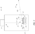
3 veranschaulicht schematisch eine beispielhafte Röntgenstrahlungsquelle, die dazu konfiguriert ist, Röntgenstrahlen gemäß gewissen hierin beschriebenen Ausführungsformen zu emittieren.3 FIG. 3 schematically illustrates an exemplary x-ray source configured to emit x-rays in accordance with certain embodiments described herein. -
4A zeigt die Abschwächungslänge von auf eine Siliziumfläche einfallenden Photonen in Abhängigkeit von der Photonenenergie gemäß gewissen hierin beschriebenen Ausführungsformen.4A Figure 11 shows the attenuation length of photons incident on a silicon surface as a function of the photon energy according to certain embodiments described herein. -
4B zeigt die Abschwächungslänge von auf eine Hafniumfläche einfallenden Photonen in Abhängigkeit von der Photonenenergie gemäß gewissen hierin beschriebenen Ausführungsformen.4B Figure 11 shows the attenuation length of photons incident on a hafnium surface as a function of the photon energy according to certain embodiments described herein. -
5A zeigt einen Verlauf der parametrischen unelastischen mittleren freien Weglänge von Elektronen in Abhängigkeit von der kinetischen Energie der Elektronen gemäß gewissen hierin beschriebenen Ausführungsformen.5A shows a curve of the parametric inelastic mean free path of electrons as a function of the kinetic energy of the electrons according to certain embodiments described herein. -
5B zeigt den Verlauf der parametrischen unelastischen mittleren freien Weglänge von Elektronen in Abhängigkeit von der kinetischen Energie der Elektronen, wobei Pfeile die Energien der Hf M5 (3d5/2) Photoelektronen, die durch drei Röntgenstahlungslinien (Si Kα1;5B shows the course of the parametric inelastic mean free path of electrons as a function of the kinetic energy of the electrons, with arrows showing the energies of the Hf M 5 (3d 5/2 ) photoelectrons, which are caused by three X-ray radiation lines (Si Kα 1 ; - Rh Kα; Cr Kα1) generiert werden, bezeichnen, und eine entsprechende Tabelle von Werten gemäß gewissen hierin beschriebenen Ausführungsformen.Rh Kα; Cr Kα 1 ) and a corresponding table of values according to certain embodiments described herein.
-
5C zeigt den Verlauf der parametrischen unelastischen mittleren freien Weglänge von Elektronen in Abhängigkeit von der kinetischen Energie der Elektronen, wobei Pfeile die Energien der Al K (Is)-Photoelektronen und der Al L (2p)-Photoelektronen, die durch drei Röntgenstrahlungslinien (Si Kα1; Rh Kα; Cr Kα1) generiert werden, bezeichnen, und eine entsprechende Tabelle von Werten gemäß gewissen hierin beschriebenen Ausführungsformen.5C shows the course of the parametric inelastic mean free path of electrons as a function of the kinetic energy of the electrons, with arrows showing the energies of the Al K (Is) photoelectrons and the Al L (2p) photoelectrons, which are caused by three X-ray lines (Si Kα 1 ; Rh Kα; Cr Kα 1 ), and a corresponding table of values according to certain embodiments described herein. -
5D zeigt den Verlauf der parametrischen unelastischen mittleren freien Weglänge von Elektronen in Abhängigkeit von der kinetischen Energie der Elektronen, wobei Pfeile die Energien der Ti K (Is)-Photoelektronen und der Ti L (2p)-Photoelektronen, die durch drei Röntgenstrahlungslinien (Si Kα1; Rh Kα; Cr Kα1) generiert werden, bezeichnen, und eine entsprechende Tabelle von Werten gemäß gewissen hierin beschriebenen Ausführungsformen.5D shows the course of the parametric inelastic mean free path of electrons as a function of the kinetic energy of the electrons, with arrows showing the energies of the Ti K (Is) photoelectrons and the Ti L (2p) photoelectrons, which are caused by three X-ray lines (Si Kα 1 ; Rh Kα; Cr Kα 1 ), and a corresponding table of values according to certain embodiments described herein. -
6 zeigt einen Verlauf der relativen Photoelektronenintensität in Abhängigkeit von der Tiefe für Si-2p-Photoelektronen, die unter Verwendung verschiedener Röntgenstrahlungsenergien gemäß gewissen hierin beschriebenen Ausführungsformen generiert werden.6th FIG. 12 shows a profile of the relative photoelectron intensity as a function of the depth for Si-2p photoelectrons which are generated using different X-ray energies in accordance with certain embodiments described herein. -
7 zeigt einen Verlauf der unelastischen mittleren freien Weglänge von Elektronen in flüssigem Wasser in Abhängigkeit von der kinetischen Energie der Elektronen gemäß gewissen hierin beschriebenen Ausführungsformen.7th shows a curve of the inelastic mean free path of electrons in liquid water as a function of the kinetic energy of the electrons according to certain embodiments described herein. -
8A veranschaulicht schematisch die Fe-2p-Photoemissionsspitzenintensität in Abhängigkeit von der Röntgenstrahlungsenergie von einem Siliziumsubstrat mit einer 1 nm dicken Fe-Schicht und einer Kohlenstoffdeckschicht mit drei Dicken von 10 nm, 20 nm und 30 nm gemäß gewissen hierin beschriebenen Ausführungsformen.8A Figure 3 illustrates schematically the Fe-2p photoemission peak intensity versus X-ray energy from a silicon substrate with a 1 nm thick Fe layer and a carbon top layer with three thicknesses of 10 nm, 20 nm and 30 nm according to certain embodiments described herein. -
8B zeigt eine Simulation der „NIST-Datenbank für die Simulation von Elektronenspektren für Flächenanalyse (Simulation of Electron Spectra for Surface Analysis - SESSA)“.8B shows a simulation of the "NIST database for the simulation of electron spectra for surface analysis (Simulation of Electron Spectra for Surface Analysis - SESSA)". -
9A veranschaulicht schematisch einen Abschnitt eines beispielhaften Systems, das einen kleinen Fokus nutzt, der Atmosphärendruck-XPS gemäß gewissen hierin beschriebenen Ausführungsformen ermöglicht.9A Figure 3 schematically illustrates a portion of an exemplary system utilizing a small focus that enables atmospheric pressure XPS in accordance with certain embodiments described herein. -
9B und9C zeigen eine beispielhafte Baugruppe einer elektrostatischen Linse bzw. ein beispielhaftes APXPS-System (das sich an der Advanced Light Source befindet) gemäß gewissen hierin beschriebenen Ausführungsformen.9B and9C -
10 zeigt beispielhafte Vorteile einer Umgebungsdruck-XPS gemäß gewissen hierin beschriebenen Ausführungsformen.10 FIG. 10 shows exemplary advantages of ambient pressure XPS in accordance with certain embodiments described herein. -
11 zeigt einen Ausgleichsdampfdruck von Wasser in Abhängigkeit von der Temperatur.11 shows an equilibrium vapor pressure of water as a function of temperature.
DETAILLIERTE BESCHREIBUNGDETAILED DESCRIPTION
Gewisse hierin beschriebene Ausführungsformen stellen in vorteilhafter Weise Emissionsröntgenstrahlen mit Energien innerhalb des Bereichs zwischen der Al Kα-Röntgenstrahlungslinie (1,49 keV) und der Ga Kα-Röntgenstrahlungslinie (9,25 keV) bereit. In gewissen Ausführungsformen werden diese Emissionsröntgenstrahlen verwendet, um in vorteilhafter Weise brauchbare Informationen bezüglich zu analysierenden Proben bereitzustellen (z. B. durch Auswählen der Emissionsröntgenstrahlungsenergie, um die Photonenquerschnitte zu optimieren).Certain embodiments described herein advantageously provide emission x-rays having energies within the range between the Al Kα x-ray line (1.49 keV) and the Ga Kα x-ray line (9.25 keV). In certain embodiments, these emission x-rays are used to advantageously provide useful information regarding samples to be analyzed (e.g., by selecting the emission x-ray energy to optimize the photon cross-sections).
Gewisse hierin beschriebene Ausführungsformen stellen eine Quelle für weiche und/oder sanfte Röntgenstrahlen bereit (z. B. weiche Röntgenstrahlen mit Energien in einem Bereich von 0,5 keV bis etwa 1,8 keV; sanfte Röntgenstrahlen mit Energien in einem Bereich von etwa 1,8 keV bis 6 keV), die über einen weiten Energiebereich zum Abstimmen der Tiefensensitivität sowie Untersuchungsgrenzflächen (z. B. gasförmig/fest; gasförmig/flüssig; flüssig/fest) auswählbar sind. Das System in gewissen Ausführungsformen ist optimiert, um einen hohen Fluss von monochromatischen und fokussierten Röntgenstrahlen bereitzustellen. Certain embodiments described herein provide a source of soft and / or gentle x-rays (e.g., soft x-rays with energies in a range of 0.5 keV to about 1.8 keV; soft x-rays with energies in a range of about 1, 8 keV to 6 keV), which can be selected over a wide energy range for adjusting the depth sensitivity and examination interfaces (e.g. gaseous / solid; gaseous / liquid; liquid / solid). The system in certain embodiments is optimized to provide high flux of monochromatic and focused x-rays.
Die Röntgenstrahlungsquelle gewisser hierin beschriebener Ausführungsformen ist an einen 4,5"-ConFlat®-Flansch montierbar, beinhaltet ein austauschbares Fenster (z. B. Be) und beinhaltet einen Mechanismus mit ausreichendem Schwenkbereich (z. B. 50 mm), um die Röntgenstrahlungsquelle relativ zu den röntgenoptischen Elementen zu bewegen und zu positionieren, ohne das Vakuum zu durchbrechen und ohne eine Neuausrichtung zu erfordern.The X-ray source of certain embodiments described herein is mountable to a 4.5 "ConFlat® flange, includes a replaceable window (e.g. Be) and includes a mechanism with sufficient pivoting range (e.g. 50 mm) around the X-ray source to move and position relative to the x-ray optical elements without breaking the vacuum and without requiring realignment.
Gewisse hierin beschriebene Ausführungsformen stellen auswählbare (z. B. abstimmbare) Röntgenstrahlungsenergien bereit (z. B. auswählbar zwischen 1,74 keV, 2,7 keV und 5,4 keV), wodurch in vorteilhafter Weise Beprobungstiefen (z. B. von 1 nm bis 15 nm) für Flächen-Grenzflächen- und Massenanalyse bereitgestellt werden, und mit optimierter Sensitivität auf ausgewählte Elemente (z. B. Hf; Al; Ti). Gewisse hierin beschriebene Ausführungsformen stellen eine hohe Röntgenstrahlungsenergieauflösung (z. B. besser als 0,7 eV für alle Energien), kleine Röntgenstrahlungsfokuspunktgrößen (z. B. in einem Bereich von 10 µm bis 200 µm; 15 µm oder weniger; 20 µm oder weniger; 100 µm oder weniger) für Analyse und Bildgebung kleiner Punkte und hohen Fluss von monochromatischen Röntgenstrahlen (z. B. mehr als 2×10⁹ Photonen/Sekunde bei 100µm Punktgröße und 200 W oder 300 W Elektronenbündelleistung; bis zu 5×10⁹ Photonen/Sekunde für Hochgeschwindigkeitsanalyse) bereit. Gewisse hierin beschriebene Ausführungsformen stellen Analyse in situ, in vitro und/oder in operando in Kombination mit kleinen Fokuspunktgrößen und hohen Anregungsenergien bereit, wodurch in vorteilhafter Weise ein Betrieb nahe Umgebungsdruck ermöglicht wird. Zum Beispiel können gewisse hierin beschriebene Ausführungsformen durch Verwendung einer Röntgenstrahlungspunktgröße von 100 µm Elektronenenergieanalysatorschlitzgrößen von 100 µm beinhalten, wodurch ein Druck in der Probenregion von etwa 20 mbar ermöglicht wird, was mit dem Dampfdruck von Wasser (z. B. etwa 17 mbar bei 15 Grad Celsius) vergleichbar ist. Bei einem weiteren Beispiel können gewisse hierin beschriebene Ausführungsformen durch Verwendung einer Röntgenstrahlungspunktgröße von 10 µm Elektronenenergieanalysatorschlitzgrößen von 10 µm aufweisen, wodurch ein Druck in der Probenregion von etwa 100 mbar oder sogar höher (z. B. 1 bar) bei einer gleichzeitigen reduzierten Signalstärke ermöglicht wird, was in vorteilhafter Weise für die Untersuchung der Katalyse verwendet werden kann. Gewisse hierin beschriebene Ausführungsformen stellen eine vollautomatisierte Auswahl der Anregungsenergie und/oder der Fokuspunktgröße ohne Kreuzkontamination unterschiedlicher Röntgenstrahlen bereit.Certain embodiments described herein provide selectable (e.g., tunable) X-ray energies (e.g., selectable between 1.74 keV, 2.7 keV and 5.4 keV), whereby sampling depths (e.g. from 1 nm to 15 nm) for surface, interface and mass analysis, and with optimized sensitivity to selected elements (e.g. Hf; Al; Ti). Certain embodiments described herein provide high x-ray energy resolution (e.g., better than 0.7 eV for all energies), small x-ray focus spot sizes (e.g., in a range of 10 µm to 200 µm; 15 µm or less; 20 µm or less ; 100 µm or less) for analysis and imaging of small points and high flow of monochromatic X-rays (e.g. more than 2 × 10 9 photons / second at 100 µm point size and 200 W or 300 W electron beam power; up to 5 × 10 9 photons / Second for high-speed analysis). Certain embodiments described herein provide analysis in situ, in vitro and / or in operando in combination with small focus point sizes and high excitation energies, which advantageously enables operation near ambient pressure. For example, certain embodiments described herein by using an X-ray spot size of 100 µm can include electron energy analyzer slot sizes of 100 µm, thereby allowing a pressure in the sample region of about 20 mbar, which is the same as the vapor pressure of water (e.g., about 17 mbar at 15 degrees Celsius) is comparable. In another example, certain embodiments described herein by using an X-ray spot size of 10 µm can have electron energy analyzer slot sizes of 10 µm, thereby enabling a pressure in the sample region of about 100 mbar or even higher (e.g. 1 bar) with a simultaneous reduced signal strength , which can be used advantageously for the study of catalysis. Certain embodiments described herein provide a fully automated selection of the excitation energy and / or the focus point size without cross-contamination of different x-rays.
Die
Während frühere Systeme Röntgenstrahlungsquellen mit Anoden beinhalteten, die eine Wärmeableitungsschicht aufweisen, die Siliziumkarbid umfasst, waren diese Röntgenstrahlungsquellen nicht dazu konfiguriert, Si-charakteristische Röntgenstrahlen (z. B. die Si Kai-Linie) zu emittieren, die im Siliziumkarbid generiert werden (siehe z. B. US-Patentanmeldung mit Veröffentlichungsnr.
In gewissen Ausführungsformen ist die mindestens eine Röntgenstrahlungsquelle
Wie schematisch durch
In gewissen Ausführungsformen umfasst die mindestens eine Schicht
In gewissen Ausführungsformen umfasst die Vielzahl von Unterquellen
In gewissen Ausführungsformen umfasst die mindestens eine Röntgenstrahlungsquelle
In gewissen Ausführungsformen umfasst das mindestens eine Ziel
Beispielhafte Parameter der mindestens einen Röntgenstrahlungsquelle
In gewissen Ausführungsformen umfasst das System
Für eine Spurenelementanalyse von Halbleiter- und geologischen Proben kann die Verwendung der Si Kai-Röntgenemissionslinien-Röntgenstrahlen in vorteilhafter Weise den Hintergrundbeitrag von Silizium in den Proben reduzieren. Da die Energie der Si Kα1-Röntgenemissionslinien-Röntgenstrahlen (etwa 1,74 keV) geringer als die Si K-Adsorptionskantenenergie ist, generieren die Si Kα1-Röntgenemissionslinien-Röntgenstrahlen keinen Hintergrund-Photoelektronen- und/oder Fluoreszenzbeitrag von Si, der zu sehen wäre, wenn Röntgenstrahlen über der Si K-Adsorptionskantenenergie verwendet würden.For trace element analysis of semiconductor and geological samples, the use of the Si Kai x-ray emission line x-rays can advantageously reduce the background contribution of silicon in the samples. Since the energy of the Si-Ka 1 -Röntgenemissionslinien X-rays (about 1.74 keV) is less than the K-Si Adsorptionskantenenergie, the Si Ka 1 -Röntgenemissionslinien X-ray photoelectron generate no background and / or fluorescence contribution of Si to the would be seen if x-rays were used above the Si K adsorption edge energy.
In gewissen Ausführungsformen, wie schematisch durch die
In gewissen Ausführungsformen umfasst das mindestens eine kollimierende röntgenoptische Element
In gewissen Ausführungsformen weist mindestens ein Abschnitt der Fläche
Das mindestens eine zweite röntgenoptische Element
Das mindestens eine dritte röntgenoptische Element
In gewissen Ausführungsformen umfasst das mindestens eine fokussierende röntgenoptische Element
In gewissen Ausführungsformen weist mindestens ein Abschnitt der Fläche
In gewissen Ausführungsformen umfasst das System
In gewissen Ausführungsformen umfasst das System
In gewissen Ausführungsformen ist jede der röntgenoptischen Anordnungen
In gewissen Ausführungsformen ist eine erste röntgenoptische Anordnung
In gewissen Ausführungsformen ist das System
In gewissen Ausführungsformen ist das System
In gewissen Ausführungsformen ist das System
TiefenselektivitätDepth selectivity
In gewissen Ausführungsformen ist das System
Zum Beispiel zeigen die
Die
Beispielhafte KonfigurationenExemplary configurations
Die
Wie schematisch durch
Wie schematisch durch
Beispielhafte KonfigurationExemplary configuration
Tabelle 1 listet verschiedene Komponenten einer beispielhaften Konfiguration eines APXPS-Systems gemäß gewissen hierin beschriebenen Ausführungsformen auf. Die beispielhafte Konfiguration kann beim Untersuchen verschiedener Prozesse und/oder Phänomenen bei Flüssig-Fest-Grenzflächen (z. B. Korrosion von metallischen Biomaterialien, wie etwa medizinische Implantate und medizinische Vorrichtungen; Flächenchemie bei realistischen Umgebungsdruckumgebungen) verwendet werden.
Tabelle 1:
Die beispielhafte Konfiguration, die mit gewissen hierin beschriebenen Ausführungsformen kompatibel ist, kann durch einen Gütefaktor (z. B. zum Vergleich mit anderen APXPS-Systemen) gekennzeichnet sein. Zum Beispiel kann der Gütefaktor zum Vergleichen unterschiedlicher APXPS-Systeme zum Untersuchen von Fest-Flüssig-Grenzflächen von Biomaterialien mit Tiefenprofilierung als die Intensität der Photoelektronenspitze (Ii) für ein interessierendes Element i bei einer Tiefe (z) von der Fläche, von der die Photoelektronen emittiert werden, ausgedrückt werden. Die Intensität Ii ist abhängig von dem Photonenfluss (F), der auf die Fläche einfällt, der durchschnittlichen Atomkonzentration des Elements i (Ni), dem Photonenquerschnitt des Elements i in Bezug auf die erwähnte Spitze (σi), die unelastische mittlere freie Weglänge (Λi,) von Photoelektronen vom Element i in Bezug auf die erwähnte Spitze und den festen Akzeptanzwinkel (Ω(hv)) des Analysators (ungefähr umgekehrt proportional zu hv). In der einfachsten Form gilt Ii = F * Ni * σi * exp (-z/Λi,) * Ω(hv) Khv, wobei Khv allen anderen Faktoren entspricht (von denen angenommen werden kann, dass sie für eine spezifische Photonenenergie während der Messung konstant bleiben).The exemplary configuration compatible with certain embodiments described herein may be characterized by a figure of merit (e.g., for comparison to other APXPS systems). For example, the figure of merit for comparing different APXPS systems for investigating solid-liquid interfaces of biomaterials with depth profiling as the intensity of the photoelectron tip (Ii) for an element of interest i at a depth (z) from the surface from which the photoelectrons be emitted, be expressed. The intensity Ii depends on the photon flux (F) incident on the surface, the average atomic concentration of the element i (Ni), the photon cross section of the element i in relation to the mentioned tip (σi), the inelastic mean free path (Λi ,) of photoelectrons from element i in relation to the mentioned tip and the fixed acceptance angle (Ω (hv)) of the analyzer (approximately inversely proportional to hv). In its simplest form, Ii = F * Ni * σi * exp (-z / Λ i ,) * Ω (hv) K hv , where K hv corresponds to all other factors (which can be assumed to be for a specific photon energy remain constant during the measurement).
In gewissen hierin beschriebenen Ausführungsformen stellt die beispielhafte Konfiguration fünf Mal mehr Fluss an der Probe als die derzeit vertriebenen APXPS-Systeme bereit. Zum Beispiel verwendet das von SPECS Surface Nano Analysis GmbH, Berlin, Deutschland vertriebene laborbasierte APXPS-System Al Ka-Röntgenstrahlen mit 1,487 keV, die aufgrund der begrenzten IMFP der Photoelektronen nicht geeignet sind zum Untersuchen von Fest-Flüssig-Grenzflächen von in-vitro-Biomaterialien (z. B. medizinische Implantate). Bei einem anderen Beispiel leidet eine Ga Ka-Röntgenstrahlungsquelle (9,3 keV), die eine Ga-Flüssigstrahlanode verwendet, die von Scienta-Omicron GmbH, Taunusstein, Deutschland vertrieben wird, an geringeren Querschnitten und somit geringeren Detektionseffizienzen (z. B. um einen Faktor 6 im Vergleich zur Verwendung von Cr Ka-Röntgenstrahlen). Zusätzlich ist der akzeptierte Festwinkel des Analysators für 9,3 keV Photoelektronen im Vergleich zu 5,4 keV Photoelektronen aufgrund größerer Verlangsamung, die durch den Analysator verwendet wird, etwa 60 % geringer, was den Festwinkel reduziert. Bei noch einem weiteren Beispiel nutzt eine Doppel-Röntgenstrahlungsquelle von Al Kα und Cr Kα, vertrieben von Ulvac-Phi, Inc., Kanagawa, Japan, als „Phi Quantes“ Bragg-Kristalle mit Rowland-Kreisgeometrie zur Monochromatisierung, was eine höhere Auflösung zu Lasten eines geringeren Flusses und eines größeren Divergenzwinkels bereitstellt.In certain embodiments described herein, the exemplary configuration provides five times more flow to the sample than the currently marketed APXPS systems. For example, the laboratory-based APXPS system sold by SPECS Surface Nano Analysis GmbH, Berlin, Germany, uses Al Ka X-rays with 1.487 keV, which are not suitable for examining solid-liquid interfaces of in vitro due to the limited IMFP of the photoelectrons. Biomaterials (e.g. medical implants). In another example, a Ga Ka x-ray source (9.3 keV) using a Ga liquid jet anode sold by Scienta-Omicron GmbH, Taunusstein, Germany, suffers from smaller cross-sections and thus lower detection efficiencies (e.g. um a factor of 6 compared to using Cr Ka X-rays). In addition, the accepted fixed angle of the analyzer for 9.3 keV photoelectrons compared to 5.4 keV photoelectrons is about 60% less due to the greater deceleration used by the analyzer, which reduces the fixed angle. In yet another example, a dual X-ray source of Al Kα and Cr Kα, sold by Ulvac-Phi, Inc., Kanagawa, Japan, uses Bragg crystals with Rowland circular geometry as "Phi Quantes" for monochromatization, which leads to higher resolution Provides loads of lesser flow and greater angle of divergence.
In gewissen hierin beschriebenen Ausführungsformen stellt die beispielhafte Konfiguration drei unterschiedliche Röntgenstrahlungsenergien bereit, wodurch eine systematische Untersuchung von Tiefenprofilierung ermöglicht und die Leistungsfähigkeit für Signalstärke optimiert wird, mit einem Gütefaktor von etwa 50 Mal größer als bei derzeit vertriebenen APXPS-Systemen (z. B. gleich etwa 5 (Fluss) × 6 (Querschnitt) × 1,6 (Akzeptanzfestwinkel)). Als Ergebnis kann die beispielhafte Konfiguration einen höheren Fluss (z. B. um einen Faktor fünf) mit deutlich größeren Querschnitten und der Fähigkeit zur Optimierung in Abhängigkeit von dem interessierenden Element und verschiedenen Dicken der Flüssigkeit und der Passivierungsschicht der Probe bereitstellen.In certain embodiments described herein, the exemplary configuration provides three different x-ray energies, thereby enabling a systematic study of depth profiling and optimizing performance for signal strength, with a figure of merit of about 50 times greater than currently marketed APXPS systems (e.g., equal to about 5 (flow) × 6 (cross section) × 1.6 (acceptance fixed angle)). As a result, the exemplary configuration can provide higher flux (e.g., by a factor of five) with significantly larger cross-sections and the ability to optimize depending on the element of interest and different thicknesses of the liquid and the passivation layer of the sample.
Konditionalsprache, wie etwa „kann“, „könnte“, „würde“ oder „möchte“, soll, sofern nicht spezifisch anders angegeben oder im verwendeten Kontext anders zu verstehen, allgemein vermitteln, dass gewisse Ausführungsformen gewisse Merkmale, Elemente und/oder Schritte beinhalten, während andere Ausführungsformen diese nicht beinhalten. Somit soll eine derartige Konditionalsprache im Allgemeinen nicht implizieren, dass Merkmale, Elemente und/oder Schritte in irgendeiner Weise für eine oder mehrere Ausführungsformen erforderlich sind.Unless specifically stated otherwise or understood differently in the context used, conditional language such as “can”, “could”, “would” or “would like” generally convey that certain embodiments include certain features, elements and / or steps while other embodiments do not include them. Thus, such conditional language is generally not intended to imply that features, elements, and / or steps are required in any way for one or more embodiments.
Konjunktivsprache, wie etwa der Ausdruck „mindestens eines von X, Y und Z“ soll, sofern nicht spezifisch anders angegeben, im verwendeten Kontext so verstanden werden, dass allgemein vermittelt wird, dass ein Gegenstand, ein Begriff usw. entweder X, Y oder Z sein kann. Somit soll derartige Konjunktivsprache im Allgemeinen nicht implizieren, dass gewisse Ausführungsformen die Anwesenheit von mindestens einem von X, mindestens einem von Y und mindestens einem von Z erfordern.Unless specifically stated otherwise, subjunctive language, such as the expression "at least one of X, Y and Z", should be understood in the context used to mean that an object, a term etc. is either X, Y or Z can be. Thus, in general, such subjunctive language is not intended to imply that certain embodiments require the presence of at least one of X, at least one of Y, and at least one of Z.
Sprache mit Abstufungen, wie hierin verwendet, wie etwa die Begriffe „ungefähr“, „etwa“, „im Allgemeinen“ und „im Wesentlichen“, stellt einen Wert, eine Menge oder eine Eigenschaft nahe dem genannten Wert, der genannten Menge oder der genannten Eigenschaft dar, der bzw. die dennoch eine gewünschte Funktion durchführt oder ein gewünschtes Ergebnis erzielt. Zum Beispiel können sich die Begriffe „ungefähr“, „etwa“, „im Allgemeinen“ und „im Wesentlichen“ auf eine Menge beziehen, die innerhalb von ± 10%, innerhalb von ± 5 %, innerhalb von ± 2 %, innerhalb von ± 1 % oder innerhalb von ± 0.1 % der genannten Menge liegt. Als ein weiteres Beispiel beziehen sich die Begriffe „im Allgemeinen parallel“ und „im Wesentlichen parallel“ auf einen Wert, eine Menge oder eine Eigenschaft, der bzw. die von genau parallel um ± 10 Grad, ± 5 Grad, ± 2 Grad, ± 1 Grad oder ± 0,1 Grad abweicht, und beziehen sich die Begriffe „im Allgemeinen senkrecht“ und „im Wesentlichen senkrecht“ auf einen Wert, eine Menge oder eine Eigenschaft, der bzw. die von genau senkrecht um ± 10 Grad, ± 5 Grad, ± 2 Grad, ± 1 Grad oder ± 0,1 Grad abweicht.Graded language, as used herein, such as the terms "approximately,""about,""generally", and "substantially" represents a value, amount, or property close to the stated value, amount or characteristic A property that nonetheless performs a desired function or achieves a desired result. For example, the terms “approximately”, “about”, “generally” and “substantially” can refer to an amount that is within ± 10%, within ± 5%, within ± 2%, within ± 1% or within ± 0.1% of the stated amount. As another example, the terms “generally parallel” and “substantially parallel” refer to a value, amount, or property that is precisely parallel by ± 10 degrees, ± 5 degrees, ± 2 degrees, ± 1 degree or ± 0.1 degree, and the terms “generally perpendicular” and “im Substantially perpendicular ”means a value, quantity or characteristic that deviates from precisely perpendicular by ± 10 degrees, ± 5 degrees, ± 2 degrees, ± 1 degree or ± 0.1 degrees.
Verschiedene Konfigurationen wurden vorstehend beschrieben. Auch wenn diese Erfindung unter Bezugnahme auf diese spezifischen Konfigurationen beschrieben wurde, sollen die Beschreibungen für die Erfindung veranschaulichend sein und sind nicht als einschränkend zu verstehen. Viele Modifikationen und Anwendungen werden dem Fachmann in den Sinn kommen, ohne vom wahren Geist und Umfang der Erfindung abzuweichen. Zum Beispiel können in jedem Verfahren oder Prozess, die hierin offenbart sind, die Handlungen oder Vorgänge, die das Verfahren/den Prozess ausmachen, in einer beliebigen geeigneten Abfolge durchgeführt werden und sind nicht notwendigerweise auf eine beliebige konkrete offenbarte Abfolge begrenzt. Merkmale oder Elemente aus verschiedenen Ausführungsformen und Beispielen, die vorstehend erörtert wurden, können miteinander kombiniert werden, um alternative Konfigurationen zu erzeugen, die mit hierin offenbarten Ausführungsformen kompatibel sind. Verschiedene Aspekte und Vorteile der Ausführungsformen wurden soweit angebracht beschrieben. Es versteht sich, dass nicht notwendigerweise alle derartigen Aspekte oder Vorteile gemäß einer konkreten Ausführungsform erreicht werden können. Somit ist zum Beispiel anzuerkennen, dass die verschiedenen Ausführungsformen in einer Weise ausgeführt werden können, die einen Vorteil oder eine Reihe von Vorteilen gemäß den Lehren hierin erreicht oder optimiert, ohne notwendigerweise andere Aspekte oder Vorteile, die hierin gelehrt oder vorgeschlagen sein können, zu erreichen.Various configurations have been described above. While this invention has been described with reference to these specific configurations, the descriptions are intended to be illustrative of the invention and are not to be considered restrictive. Many modifications and applications will come to mind to those skilled in the art without departing from the true spirit and scope of the invention. For example, in each method or process disclosed herein, the acts or acts that comprise the method / process can be performed in any suitable sequence and are not necessarily limited to any particular sequence disclosed. Features or elements from various embodiments and examples discussed above can be combined with one another to create alternative configurations compatible with embodiments disclosed herein. Various aspects and advantages of the embodiments have been described as appropriate. It is understood that not necessarily all such aspects or advantages can be achieved in accordance with a specific embodiment. Thus, for example, it should be recognized that the various embodiments can be practiced in a manner that achieves or optimizes a benefit or series of advantages according to the teachings herein without necessarily achieving other aspects or advantages that may be taught or suggested herein .
ZITATE ENTHALTEN IN DER BESCHREIBUNGQUOTES INCLUDED IN THE DESCRIPTION
Diese Liste der vom Anmelder aufgeführten Dokumente wurde automatisiert erzeugt und ist ausschließlich zur besseren Information des Lesers aufgenommen. Die Liste ist nicht Bestandteil der deutschen Patent- bzw. Gebrauchsmusteranmeldung. Das DPMA übernimmt keinerlei Haftung für etwaige Fehler oder Auslassungen.This list of the documents listed by the applicant was generated automatically and is included solely for the better information of the reader. The list is not part of the German patent or utility model application. The DPMA assumes no liability for any errors or omissions.
Zitierte PatentliteraturPatent literature cited
- US 62728574 B [0001]US 62728574 B [0001]
- US 2014/0185778 [0015]US 2014/0185778 [0015]
- US 5944963 A [0018]US 5944963 A [0018]
- US 9874531 [0023, 0035]US 9874531 [0023, 0035]
- US 9823203 [0023, 0035]US 9823203 [0023, 0035]
- US 9719947 [0023, 0035]US 9719947 [0023, 0035]
- US 9594036 [0023, 0035]US 9594036 [0023, 0035]
- US 9570265 [0023, 0035]US 9570265 [0023, 0035]
- US 9543109 [0023, 0035]US 9543109 [0023, 0035]
- US 9449781 [0023, 0035]US 9449781 [0023, 0035]
- US 9448190 [0023, 0035]US 9448190 [0023, 0035]
- US 9390881 [0023, 0035]US 9390881 [0023, 0035]
- US 9874531 B [0027, 0030, 0031, 0034]US 9874531 B [0027, 0030, 0031, 0034]
- US 9823203 B [0027, 0030, 0031, 0034, 0036]US 9823203 B [0027, 0030, 0031, 0034, 0036]
- US 9719947 B [0027, 0030, 0031, 0034]US 9719947 B [0027, 0030, 0031, 0034]
- US 9594036 B [0027, 0030, 0031, 0034, 0036]US 9594036 B [0027, 0030, 0031, 0034, 0036]
- US 9570265 B [0027, 0030, 0031, 0034]US 9570265 B [0027, 0030, 0031, 0034]
- US 9543109 B [0027, 0030, 0031, 0034]US 9543109 B [0027, 0030, 0031, 0034]
- US 9449781 B [0027, 0030, 0031, 0034]US 9449781 B [0027, 0030, 0031, 0034]
- US 9448190 B [0027, 0030, 0031, 0034]US 9448190 B [0027, 0030, 0031, 0034]
- US 9390881 B [0027, 0030, 0031, 0034]US 9390881 B [0027, 0030, 0031, 0034]
Zitierte Nicht-PatentliteraturNon-patent literature cited
- Emfietzoglou & Nikjoo, Radiation Research 2007 [0051]Emfietzoglou & Nikjoo, Radiation Research 2007 [0051]
- Stafanos u.a., Nature Scientific Report, 2013 [0052]Stafanos et al., Nature Scientific Report, 2013 [0052]
Claims (34)
Applications Claiming Priority (3)
| Application Number | Priority Date | Filing Date | Title |
|---|---|---|---|
| US201862728574P | 2018-09-07 | 2018-09-07 | |
| US62/728,574 | 2018-09-07 | ||
| PCT/US2019/049553 WO2020051221A2 (en) | 2018-09-07 | 2019-09-04 | System and method for depth-selectable x-ray analysis |
Publications (1)
| Publication Number | Publication Date |
|---|---|
| DE112019004478T5 true DE112019004478T5 (en) | 2021-07-08 |
Family
ID=69722613
Family Applications (1)
| Application Number | Title | Priority Date | Filing Date |
|---|---|---|---|
| DE112019004478.8T Pending DE112019004478T5 (en) | 2018-09-07 | 2019-09-04 | SYSTEM AND PROCEDURE FOR X-RAY ANALYSIS WITH SELECTABLE DEPTH |
Country Status (4)
| Country | Link |
|---|---|
| US (1) | US11056308B2 (en) |
| CN (1) | CN112823280B (en) |
| DE (1) | DE112019004478T5 (en) |
| WO (1) | WO2020051221A2 (en) |
Families Citing this family (26)
| Publication number | Priority date | Publication date | Assignee | Title |
|---|---|---|---|---|
| WO2010120377A2 (en) | 2009-04-16 | 2010-10-21 | Silver Eric H | Monochromatic x-ray methods and apparatus |
| US20150369758A1 (en) | 2014-06-24 | 2015-12-24 | Eric H. Silver | Methods and apparatus for determining information regarding chemical composition using x-ray radiation |
| KR102658750B1 (en) | 2017-05-19 | 2024-04-22 | 이매진 싸이언티픽, 인크. | Monochromatic X-ray imaging system and method |
| CA3129632A1 (en) | 2018-02-09 | 2019-08-15 | Imagine Scientific, Inc. | Monochromatic x-ray imaging systems and methods |
| WO2020056281A1 (en) * | 2018-09-14 | 2020-03-19 | Imagine Scientific, Inc. | Monochromatic x-ray component systems and methods |
| WO2020132360A1 (en) * | 2018-12-20 | 2020-06-25 | Arizona Board Of Regents On Behalf Of Arizona State University | Off-axis capillary x-ray optics |
| JP7705852B2 (en) * | 2019-10-24 | 2025-07-10 | ノヴァ メジャリング インスツルメンツ インコーポレイテッド | Patterned X-ray emitting target |
| JP7572033B2 (en) * | 2020-10-23 | 2024-10-23 | 株式会社リガク | Imaging X-ray microscope |
| CN116472474A (en) * | 2020-11-25 | 2023-07-21 | 浜松光子学株式会社 | Image pickup unit and image pickup system |
| US12480892B2 (en) | 2020-12-07 | 2025-11-25 | Sigray, Inc. | High throughput 3D x-ray imaging system using a transmission x-ray source |
| DE112021006348T5 (en) | 2020-12-07 | 2023-09-21 | Sigray, Inc. | HIGH-THROUGHPUT 3D X-RAY IMAGING SYSTEM USING A TRANSMISSION X-RAY SOURCE |
| EP4145117A1 (en) | 2021-09-01 | 2023-03-08 | Malvern Panalytical B.V. | Adaptable x-ray analysis apparatus |
| DE112023000574T5 (en) | 2022-01-13 | 2024-10-24 | Sigray, Inc. | MICROFOCUS X-RAY SOURCE FOR GENERATING HIGH FLUX AND LOW ENERGY X-RAYS |
| US20230243762A1 (en) * | 2022-01-28 | 2023-08-03 | National Technology & Engineering Solutions Of Sandia, Llc | Multi-material patterned anode systems |
| WO2023168204A1 (en) | 2022-03-02 | 2023-09-07 | Sigray, Inc. | X-ray fluorescence system and x-ray source with electrically insulative target material |
| CN114594121B (en) * | 2022-03-04 | 2022-11-29 | 南开大学 | High-flux XPS device, detection method and application |
| DE112023001408T5 (en) | 2022-03-15 | 2025-02-13 | Sigray, Inc. | SYSTEM AND METHOD FOR COMPACT LAMINOGRAPHY USING A MICROFOCUS TRANSMISSION X-RAY SOURCE AND A VARIABLE MAGNIFICATION X-RAY DETECTOR |
| JP2025515085A (en) | 2022-05-02 | 2025-05-13 | シグレイ、インコーポレイテッド | X-ray sequential array wavelength dispersive spectrometer |
| KR102893593B1 (en) * | 2022-11-23 | 2025-12-04 | 주식회사 월드빔솔루션 | Electron beam based extreme ultraviolet light source apparatus |
| WO2024173256A1 (en) | 2023-02-16 | 2024-08-22 | Sigray, Inc. | X-ray detector system with at least two stacked flat bragg diffractors |
| EP4425158A1 (en) * | 2023-03-03 | 2024-09-04 | Malvern Panalytical B.V. | X-ray analysis apparatus and method |
| US12181423B1 (en) | 2023-09-07 | 2024-12-31 | Sigray, Inc. | Secondary image removal using high resolution x-ray transmission sources |
| US12429437B2 (en) | 2023-11-07 | 2025-09-30 | Sigray, Inc. | System and method for x-ray absorption spectroscopy using spectral information from two orthogonal planes |
| WO2025151383A1 (en) | 2024-01-08 | 2025-07-17 | Sigray, Inc. | X-ray analysis system with focused x-ray beam and non-x-ray microscope |
| WO2025155719A1 (en) | 2024-01-18 | 2025-07-24 | Sigray, Inc. | Sequential array of x-ray imaging detectors |
| US12431256B2 (en) | 2024-02-15 | 2025-09-30 | Sigray, Inc. | System and method for generating a focused x-ray beam |
Citations (11)
| Publication number | Priority date | Publication date | Assignee | Title |
|---|---|---|---|---|
| US5944963A (en) | 1994-01-21 | 1999-08-31 | The Carborundum Company | Method of coating a substrate with a SiCx film |
| US20140185778A1 (en) | 2012-12-28 | 2014-07-03 | General Electric Company | Multilayer x-ray source target with high thermal conductivity |
| US9390881B2 (en) | 2013-09-19 | 2016-07-12 | Sigray, Inc. | X-ray sources using linear accumulation |
| US9448190B2 (en) | 2014-06-06 | 2016-09-20 | Sigray, Inc. | High brightness X-ray absorption spectroscopy system |
| US9449781B2 (en) | 2013-12-05 | 2016-09-20 | Sigray, Inc. | X-ray illuminators with high flux and high flux density |
| US9543109B2 (en) | 2013-09-19 | 2017-01-10 | Sigray, Inc. | X-ray sources using linear accumulation |
| US9570265B1 (en) | 2013-12-05 | 2017-02-14 | Sigray, Inc. | X-ray fluorescence system with high flux and high flux density |
| US9594036B2 (en) | 2014-02-28 | 2017-03-14 | Sigray, Inc. | X-ray surface analysis and measurement apparatus |
| US9719947B2 (en) | 2013-10-31 | 2017-08-01 | Sigray, Inc. | X-ray interferometric imaging system |
| US9823203B2 (en) | 2014-02-28 | 2017-11-21 | Sigray, Inc. | X-ray surface analysis and measurement apparatus |
| US9874531B2 (en) | 2013-10-31 | 2018-01-23 | Sigray, Inc. | X-ray method for the measurement, characterization, and analysis of periodic structures |
Family Cites Families (539)
| Publication number | Priority date | Publication date | Assignee | Title |
|---|---|---|---|---|
| US1355126A (en) | 1916-12-16 | 1920-10-12 | Gen Electric | X-ray tube |
| US1203495A (en) | 1913-05-09 | 1916-10-31 | Gen Electric | Vacuum-tube. |
| US1211092A (en) | 1915-06-05 | 1917-01-02 | Gen Electric | X-ray tube. |
| US1215116A (en) | 1916-10-24 | 1917-02-06 | Gen Electric | X-ray apparatus. |
| US1328495A (en) | 1918-07-15 | 1920-01-20 | Gen Electric | X-ray apparatus |
| US1790073A (en) | 1927-07-02 | 1931-01-27 | Pohl Ernst | Rontgen tube |
| BE355009A (en) | 1927-10-18 | |||
| US1917099A (en) | 1929-10-18 | 1933-07-04 | Gen Electric | x-ray tube |
| US2926270A (en) | 1957-12-30 | 1960-02-23 | Gen Electric | Rotating anode x-ray tube |
| US3795832A (en) | 1972-02-28 | 1974-03-05 | Machlett Lab Inc | Target for x-ray tubes |
| US4165472A (en) | 1978-05-12 | 1979-08-21 | Rockwell International Corporation | Rotating anode x-ray source and cooling technique therefor |
| US4266138A (en) | 1978-07-11 | 1981-05-05 | Cornell Research Foundation, Inc. | Diamond targets for producing high intensity soft x-rays and a method of exposing x-ray resists |
| US4192994A (en) | 1978-09-18 | 1980-03-11 | The United States Of America As Represented By The Administrator Of The National Aeronautics And Space Administration | Diffractoid grating configuration for X-ray and ultraviolet focusing |
| US4227112A (en) | 1978-11-20 | 1980-10-07 | The Machlett Laboratories, Inc. | Gradated target for X-ray tubes |
| JPS5744841A (en) | 1980-09-01 | 1982-03-13 | Hitachi Ltd | Method and apparatus for x-ray diffraction |
| DE3222511C2 (en) | 1982-06-16 | 1985-08-29 | Feinfocus Röntgensysteme GmbH, 3050 Wunstorf | Fine focus X-ray tube |
| US4523327A (en) | 1983-01-05 | 1985-06-11 | The United States Of America As Represented By The Secretary Of The Air Force | Multi-color X-ray line source |
| US4727000A (en) | 1983-06-06 | 1988-02-23 | Ovonic Synthetic Materials Co., Inc. | X-ray dispersive and reflective structures |
| FR2548447B1 (en) | 1983-06-28 | 1986-02-21 | Thomson Csf | HIGH INTENSITY FIREPLACE X-RAY TUBE |
| US4807268A (en) | 1983-11-04 | 1989-02-21 | University Of Southern California | Scanning monochrometer crystal and method of formation |
| US4642811A (en) | 1984-06-12 | 1987-02-10 | Northwestern University | EXAFS spectrometer |
| US4798446A (en) | 1987-09-14 | 1989-01-17 | The United States Of America As Represented By The United States Department Of Energy | Aplanatic and quasi-aplanatic diffraction gratings |
| US4945552A (en) | 1987-12-04 | 1990-07-31 | Hitachi, Ltd. | Imaging system for obtaining X-ray energy subtraction images |
| JPH0631887B2 (en) | 1988-04-28 | 1994-04-27 | 株式会社東芝 | X-ray mirror and manufacturing method thereof |
| US5001737A (en) | 1988-10-24 | 1991-03-19 | Aaron Lewis | Focusing and guiding X-rays with tapered capillaries |
| US4951304A (en) | 1989-07-12 | 1990-08-21 | Adelphi Technology Inc. | Focused X-ray source |
| US5249216B1 (en) | 1989-10-19 | 1996-11-05 | Sumitomo Electric Industries | Total reflection x-ray fluorescence apparatus |
| US5008918A (en) | 1989-11-13 | 1991-04-16 | General Electric Company | Bonding materials and process for anode target in an x-ray tube |
| EP0432568A3 (en) | 1989-12-11 | 1991-08-28 | General Electric Company | X ray tube anode and tube having same |
| US4972449A (en) | 1990-03-19 | 1990-11-20 | General Electric Company | X-ray tube target |
| US5204887A (en) | 1990-06-01 | 1993-04-20 | Canon Kabushiki Kaisha | X-ray microscope |
| US5173928A (en) | 1990-07-09 | 1992-12-22 | Hitachi, Ltd. | Tomograph using phase information of a signal beam having transmitted through a to-be-inspected object |
| JPH0769477B2 (en) | 1990-09-05 | 1995-07-31 | 理学電機工業株式会社 | X-ray spectrometer |
| US5119408A (en) | 1990-10-31 | 1992-06-02 | General Electric Company | Rotate/rotate method and apparatus for computed tomography x-ray inspection of large objects |
| US5148462A (en) | 1991-04-08 | 1992-09-15 | Moltech Corporation | High efficiency X-ray anode sources |
| JPH0582419A (en) | 1991-09-20 | 1993-04-02 | Fujitsu Ltd | X-ray transmissive window and its manufacture |
| US5452142A (en) | 1992-10-20 | 1995-09-19 | Hughes Aircraft Company | Approach for positioning, fabricating, aligning and testing grazing, convex, hyperbolic mirrors |
| JPH06167599A (en) * | 1992-11-27 | 1994-06-14 | Nikon Corp | Production method for multilayer film mirror for x-ray |
| JPH06188092A (en) | 1992-12-17 | 1994-07-08 | Hitachi Ltd | X-ray generation target, X-ray source, and X-ray imaging device |
| US5371774A (en) | 1993-06-24 | 1994-12-06 | Wisconsin Alumni Research Foundation | X-ray lithography beamline imaging system |
| JPH0720293A (en) | 1993-06-30 | 1995-01-24 | Canon Inc | X-ray mirror, X-ray exposure apparatus using the same, and device manufacturing method |
| JPH0756000A (en) | 1993-08-17 | 1995-03-03 | Ishikawajima Harima Heavy Ind Co Ltd | Micro X-ray target |
| GB9318197D0 (en) | 1993-09-02 | 1993-10-20 | Medical Res Council | Improvements in or relating xo x-ray tubes |
| JP3512874B2 (en) | 1993-11-26 | 2004-03-31 | 株式会社東芝 | X-ray computed tomography equipment |
| DE69425631T2 (en) | 1993-11-26 | 2001-04-19 | Kabushiki Kaisha Toshiba, Kawasaki | Computer tomograph |
| US5737387A (en) | 1994-03-11 | 1998-04-07 | Arch Development Corporation | Cooling for a rotating anode X-ray tube |
| JP3191554B2 (en) | 1994-03-18 | 2001-07-23 | 株式会社日立製作所 | X-ray imaging device |
| ATE169769T1 (en) | 1994-05-11 | 1998-08-15 | Univ Colorado | X-RAY OPTICS WITH STRIKING INCIDENT LIGHT AND SPHERICAL MIRRORS |
| US5646976A (en) | 1994-08-01 | 1997-07-08 | Osmic, Inc. | Optical element of multilayered thin film for X-rays and neutrons |
| JP3612795B2 (en) | 1994-08-20 | 2005-01-19 | 住友電気工業株式会社 | X-ray generator |
| US5878110A (en) | 1994-08-20 | 1999-03-02 | Sumitomo Electric Industries, Ltd. | X-ray generation apparatus |
| JPH08128971A (en) | 1994-10-31 | 1996-05-21 | Rigaku Corp | Exafs measuring device |
| JPH08184572A (en) | 1995-01-04 | 1996-07-16 | Hitachi Ltd | Total reflection X-ray analyzer |
| DE19509516C1 (en) | 1995-03-20 | 1996-09-26 | Medixtec Gmbh Medizinische Ger | Microfocus X-ray device |
| JPH095500A (en) | 1995-06-26 | 1997-01-10 | Shimadzu Corp | X-ray microscope |
| US5729583A (en) | 1995-09-29 | 1998-03-17 | The United States Of America As Represented By The Secretary Of Commerce | Miniature x-ray source |
| US5682415A (en) | 1995-10-13 | 1997-10-28 | O'hara; David B. | Collimator for x-ray spectroscopy |
| JPH09187455A (en) | 1996-01-10 | 1997-07-22 | Hitachi Ltd | Phase type X-ray CT system |
| US5602899A (en) | 1996-01-31 | 1997-02-11 | Physical Electronics Inc. | Anode assembly for generating x-rays and instrument with such anode assembly |
| US5778039A (en) | 1996-02-21 | 1998-07-07 | Advanced Micro Devices, Inc. | Method and apparatus for the detection of light elements on the surface of a semiconductor substrate using x-ray fluorescence (XRF) |
| EP0799600B1 (en) | 1996-03-29 | 2004-09-08 | Hitachi, Ltd. | Phase-contrast X-ray imaging system |
| US5912940A (en) | 1996-06-10 | 1999-06-15 | O'hara; David | Combination wavelength and energy dispersive x-ray spectrometer |
| US5825848A (en) | 1996-09-13 | 1998-10-20 | Varian Associates, Inc. | X-ray target having big Z particles imbedded in a matrix |
| US5772903A (en) | 1996-09-27 | 1998-06-30 | Hirsch; Gregory | Tapered capillary optics |
| IL132351A (en) | 1997-04-08 | 2003-03-12 | X Ray Technologies Pty Ltd | High resolution x-ray imaging of very small objects |
| US5812629A (en) | 1997-04-30 | 1998-09-22 | Clauser; John F. | Ultrahigh resolution interferometric x-ray imaging |
| WO1999009401A1 (en) | 1997-08-15 | 1999-02-25 | Hara David B O | Apparatus and method for improved energy dispersive x-ray spectrometer |
| US6108397A (en) | 1997-11-24 | 2000-08-22 | Focused X-Rays, Llc | Collimator for x-ray proximity lithography |
| JPH11304728A (en) | 1998-04-23 | 1999-11-05 | Hitachi Ltd | X-ray measurement device |
| DE19820861B4 (en) | 1998-05-09 | 2004-09-16 | Bruker Axs Gmbh | Simultaneous X-ray fluorescence spectrometer |
| JP3712531B2 (en) | 1998-06-10 | 2005-11-02 | 株式会社リガク | XAFS measurement method and XAFS measurement apparatus |
| US6108398A (en) | 1998-07-13 | 2000-08-22 | Jordan Valley Applied Radiation Ltd. | X-ray microfluorescence analyzer |
| GB9815968D0 (en) | 1998-07-23 | 1998-09-23 | Bede Scient Instr Ltd | X-ray focusing apparatus |
| US6118853A (en) | 1998-10-06 | 2000-09-12 | Cardiac Mariners, Inc. | X-ray target assembly |
| WO2000031523A2 (en) | 1998-11-25 | 2000-06-02 | Koninklijke Philips Electronics N.V. | X-ray analysis apparatus including a parabolic x-ray mirror and a crystal monochromator |
| US6125167A (en) | 1998-11-25 | 2000-09-26 | Picker International, Inc. | Rotating anode x-ray tube with multiple simultaneously emitting focal spots |
| AU3474200A (en) | 1999-01-26 | 2000-08-07 | Focused X-Rays Llc | X-ray interferometer |
| JP2000306533A (en) | 1999-02-19 | 2000-11-02 | Toshiba Corp | Transmission radiation type X-ray tube and method of manufacturing the same |
| US6181773B1 (en) | 1999-03-08 | 2001-01-30 | Direct Radiography Corp. | Single-stroke radiation anti-scatter device for x-ray exposure window |
| US6389100B1 (en) | 1999-04-09 | 2002-05-14 | Osmic, Inc. | X-ray lens system |
| JP2001021507A (en) | 1999-07-05 | 2001-01-26 | Rigaku Corp | Xafs measuring apparatus |
| US6278764B1 (en) | 1999-07-22 | 2001-08-21 | The Regents Of The Unviersity Of California | High efficiency replicated x-ray optics and fabrication method |
| JP2001035428A (en) | 1999-07-22 | 2001-02-09 | Shimadzu Corp | X-ray generator |
| DE19934987B4 (en) | 1999-07-26 | 2004-11-11 | Fraunhofer-Gesellschaft zur Förderung der angewandten Forschung e.V. | X-ray anode and its use |
| US6421417B1 (en) | 1999-08-02 | 2002-07-16 | Osmic, Inc. | Multilayer optics with adjustable working wavelength |
| JP3488843B2 (en) | 1999-08-26 | 2004-01-19 | 理学電機株式会社 | X-ray spectrometer and XAFS measurement device |
| US6307916B1 (en) | 1999-09-14 | 2001-10-23 | General Electric Company | Heat pipe assisted cooling of rotating anode x-ray tubes |
| US6381303B1 (en) | 1999-09-29 | 2002-04-30 | Jordan Valley Applied Radiation Ltd. | X-ray microanalyzer for thin films |
| DE19955392A1 (en) | 1999-11-18 | 2001-05-23 | Philips Corp Intellectual Pty | Monochromatic x-ray source |
| GB9927555D0 (en) | 1999-11-23 | 2000-01-19 | Bede Scient Instr Ltd | X-ray fluorescence apparatus |
| TWI282909B (en) | 1999-12-23 | 2007-06-21 | Asml Netherlands Bv | Lithographic apparatus and a method for manufacturing a device |
| AU2001233057A1 (en) | 2000-01-27 | 2001-08-14 | The University Of Chicago | Patterning of nanocrystalline diamond films for diamond microstructures useful in mems and other devices |
| US6504902B2 (en) | 2000-04-10 | 2003-01-07 | Rigaku Corporation | X-ray optical device and multilayer mirror for small angle scattering system |
| US20030054133A1 (en) | 2000-08-07 | 2003-03-20 | Wadley Hadyn N.G. | Apparatus and method for intra-layer modulation of the material deposition and assist beam and the multilayer structure produced therefrom |
| UA59495C2 (en) | 2000-08-07 | 2003-09-15 | Мурадін Абубєкіровіч Кумахов | X-ray system for measurements and tests |
| US6815363B2 (en) | 2000-08-11 | 2004-11-09 | The Regents Of The University Of California | Method for nanomachining high aspect ratio structures |
| US6891627B1 (en) | 2000-09-20 | 2005-05-10 | Kla-Tencor Technologies Corp. | Methods and systems for determining a critical dimension and overlay of a specimen |
| US6829327B1 (en) | 2000-09-22 | 2004-12-07 | X-Ray Optical Systems, Inc. | Total-reflection x-ray fluorescence apparatus and method using a doubly-curved optic |
| US6553096B1 (en) | 2000-10-06 | 2003-04-22 | The University Of North Carolina Chapel Hill | X-ray generating mechanism using electron field emission cathode |
| US6445769B1 (en) | 2000-10-25 | 2002-09-03 | Koninklijke Philips Electronics N.V. | Internal bearing cooling using forced air |
| US6463123B1 (en) | 2000-11-09 | 2002-10-08 | Steris Inc. | Target for production of x-rays |
| US6847699B2 (en) | 2000-12-04 | 2005-01-25 | Advanced Ceramics Research, Inc. | Composite components for use in high temperature applications |
| US6430260B1 (en) | 2000-12-29 | 2002-08-06 | General Electric Company | X-ray tube anode cooling device and systems incorporating same |
| JP2002336232A (en) | 2001-05-16 | 2002-11-26 | Fuji Photo Film Co Ltd | Phase-contrast image generation method and device, and program |
| DE60213994T2 (en) | 2001-06-19 | 2006-12-07 | X-Ray Optical Systems, Inc., East Greenbush | WAVE LENGTH-DISPERSIVE X-RAY FLUORESCENT SYSTEM WITH FOCUSING SOUND OPTICS AND A FOCUSING MONOCHROMATOR FOR COLLAPSE |
| US6914723B2 (en) | 2001-11-09 | 2005-07-05 | Xradia, Inc. | Reflective lithography mask inspection tool based on achromatic Fresnel optics |
| US6917472B1 (en) | 2001-11-09 | 2005-07-12 | Xradia, Inc. | Achromatic fresnel optics for ultraviolet and x-ray radiation |
| JP2003149392A (en) | 2001-11-09 | 2003-05-21 | Tohken Co Ltd | X-ray enhanced reflector and X-ray inspection device |
| WO2003049510A2 (en) | 2001-12-04 | 2003-06-12 | X-Ray Optical Systems, Inc. | X-ray source assembly having enhanced output stability, and fluid stream analysis applications thereof |
| DE10162093A1 (en) | 2001-12-18 | 2003-07-10 | Bruker Axs Gmbh | X-ray optical system with an aperture in the focus of an X-ray mirror |
| JP2003297891A (en) | 2002-01-31 | 2003-10-17 | Rigaku Industrial Co | X-ray fluorescence analyzer for semiconductors |
| WO2003065772A2 (en) | 2002-01-31 | 2003-08-07 | The Johns Hopkins University | X-ray source and method for producing selectable x-ray wavelength |
| DE10391780D2 (en) | 2002-03-26 | 2005-02-17 | Fraunhofer Ges Forschung | X-ray source with a small focal spot size |
| JP2003288853A (en) | 2002-03-27 | 2003-10-10 | Toshiba Corp | X-ray equipment |
| US7180981B2 (en) | 2002-04-08 | 2007-02-20 | Nanodynamics-88, Inc. | High quantum energy efficiency X-ray tube and targets |
| JP4322470B2 (en) | 2002-05-09 | 2009-09-02 | 浜松ホトニクス株式会社 | X-ray generator |
| US6560315B1 (en) | 2002-05-10 | 2003-05-06 | Ge Medical Systems Global Technology Company, Llc | Thin rotating plate target for X-ray tube |
| US20050282300A1 (en) | 2002-05-29 | 2005-12-22 | Xradia, Inc. | Back-end-of-line metallization inspection and metrology microscopy system and method using x-ray fluorescence |
| US7245696B2 (en) | 2002-05-29 | 2007-07-17 | Xradia, Inc. | Element-specific X-ray fluorescence microscope and method of operation |
| JP2004089445A (en) | 2002-08-30 | 2004-03-25 | Konica Minolta Holdings Inc | X ray generating apparatus and x-ray image photographing system |
| US6763086B2 (en) | 2002-09-05 | 2004-07-13 | Osmic, Inc. | Method and apparatus for detecting boron in x-ray fluorescence spectroscopy |
| DE10241423B4 (en) | 2002-09-06 | 2007-08-09 | Siemens Ag | Method of making and applying a anti-scatter grid or collimator to an X-ray or gamma detector |
| US7015467B2 (en) | 2002-10-10 | 2006-03-21 | Applied Materials, Inc. | Generating electrons with an activated photocathode |
| US7268945B2 (en) | 2002-10-10 | 2007-09-11 | Xradia, Inc. | Short wavelength metrology imaging system |
| JP3998556B2 (en) | 2002-10-17 | 2007-10-31 | 株式会社東研 | High resolution X-ray microscope |
| US7365909B2 (en) | 2002-10-17 | 2008-04-29 | Xradia, Inc. | Fabrication methods for micro compounds optics |
| US10638994B2 (en) | 2002-11-27 | 2020-05-05 | Hologic, Inc. | X-ray mammography with tomosynthesis |
| US6947522B2 (en) | 2002-12-20 | 2005-09-20 | General Electric Company | Rotating notched transmission x-ray for multiple focal spots |
| WO2004058070A1 (en) | 2002-12-26 | 2004-07-15 | Atsushi Momose | X-ray imaging system and imaging method |
| US7119953B2 (en) | 2002-12-27 | 2006-10-10 | Xradia, Inc. | Phase contrast microscope for short wavelength radiation and imaging method |
| US7079625B2 (en) | 2003-01-20 | 2006-07-18 | Siemens Aktiengesellschaft | X-ray anode having an electron incident surface scored by microslits |
| GB0309374D0 (en) | 2003-04-25 | 2003-06-04 | Cxr Ltd | X-ray sources |
| GB0812864D0 (en) | 2008-07-15 | 2008-08-20 | Cxr Ltd | Coolign anode |
| GB0525593D0 (en) | 2005-12-16 | 2006-01-25 | Cxr Ltd | X-ray tomography inspection systems |
| US8094784B2 (en) | 2003-04-25 | 2012-01-10 | Rapiscan Systems, Inc. | X-ray sources |
| US6707883B1 (en) | 2003-05-05 | 2004-03-16 | Ge Medical Systems Global Technology Company, Llc | X-ray tube targets made with high-strength oxide-dispersion strengthened molybdenum alloy |
| US7006596B1 (en) | 2003-05-09 | 2006-02-28 | Kla-Tencor Technologies Corporation | Light element measurement |
| US7280634B2 (en) | 2003-06-13 | 2007-10-09 | Osmic, Inc. | Beam conditioning system with sequential optic |
| JP5392982B2 (en) | 2003-06-13 | 2014-01-22 | オスミック、インコーポレイテッド | Beam adjustment system |
| US6975703B2 (en) | 2003-08-01 | 2005-12-13 | General Electric Company | Notched transmission target for a multiple focal spot X-ray source |
| US7023955B2 (en) | 2003-08-12 | 2006-04-04 | X-Ray Optical System, Inc. | X-ray fluorescence system with apertured mask for analyzing patterned surfaces |
| US7003077B2 (en) | 2003-10-03 | 2006-02-21 | General Electric Company | Method and apparatus for x-ray anode with increased coverage |
| US7057187B1 (en) | 2003-11-07 | 2006-06-06 | Xradia, Inc. | Scintillator optical system and method of manufacture |
| US7170969B1 (en) | 2003-11-07 | 2007-01-30 | Xradia, Inc. | X-ray microscope capillary condenser system |
| US7394890B1 (en) | 2003-11-07 | 2008-07-01 | Xradia, Inc. | Optimized x-ray energy for high resolution imaging of integrated circuits structures |
| US7218703B2 (en) | 2003-11-21 | 2007-05-15 | Tohken Co., Ltd. | X-ray microscopic inspection apparatus |
| US7130375B1 (en) | 2004-01-14 | 2006-10-31 | Xradia, Inc. | High resolution direct-projection type x-ray microtomography system using synchrotron or laboratory-based x-ray source |
| US7023950B1 (en) | 2004-02-11 | 2006-04-04 | Martin Annis | Method and apparatus for determining the position of an x-ray cone beam produced by a scanning electron beam |
| US7215736B1 (en) | 2004-03-05 | 2007-05-08 | Xradia, Inc. | X-ray micro-tomography system optimized for high resolution, throughput, image quality |
| US7203281B2 (en) | 2004-03-11 | 2007-04-10 | Varian Medical Systems, Inc. | Encapsulated stator assembly for an x-ray tube |
| DE102004013620B4 (en) | 2004-03-19 | 2008-12-04 | GE Homeland Protection, Inc., Newark | Electron window for a liquid metal anode, liquid metal anode, X-ray source and method of operating such an X-ray source |
| JP2005276760A (en) | 2004-03-26 | 2005-10-06 | Shimadzu Corp | X-ray generator |
| JP4189770B2 (en) | 2004-04-08 | 2008-12-03 | 独立行政法人科学技術振興機構 | X-ray target and apparatus using the same |
| US7286640B2 (en) | 2004-04-09 | 2007-10-23 | Xradia, Inc. | Dual-band detector system for x-ray imaging of biological samples |
| US7412024B1 (en) | 2004-04-09 | 2008-08-12 | Xradia, Inc. | X-ray mammography |
| US7330533B2 (en) | 2004-05-05 | 2008-02-12 | Lawrence Livermore National Security, Llc | Compact x-ray source and panel |
| WO2005109969A2 (en) | 2004-05-05 | 2005-11-17 | The Regents Of The University Of California | Compact x-ray source and panel |
| US6870172B1 (en) | 2004-05-21 | 2005-03-22 | Kla-Tencor Technologies Corporation | Maskless reflection electron beam projection lithography |
| US7218700B2 (en) | 2004-05-28 | 2007-05-15 | General Electric Company | System for forming x-rays and method for using same |
| US7095822B1 (en) | 2004-07-28 | 2006-08-22 | Xradia, Inc. | Near-field X-ray fluorescence microprobe |
| US7365918B1 (en) | 2004-08-10 | 2008-04-29 | Xradia, Inc. | Fast x-ray lenses and fabrication method therefor |
| US7103138B2 (en) | 2004-08-24 | 2006-09-05 | The Board Of Trustees Of The Leland Stanford Junior University | Sampling in volumetric computed tomography |
| US7120228B2 (en) | 2004-09-21 | 2006-10-10 | Jordan Valley Applied Radiation Ltd. | Combined X-ray reflectometer and diffractometer |
| WO2006050891A2 (en) | 2004-11-09 | 2006-05-18 | Carl Zeiss Smt Ag | A high-precision optical surface prepared by sagging from a masterpiece |
| US7298882B2 (en) | 2005-02-15 | 2007-11-20 | Siemens Aktiengesellschaft | Generalized measure of image quality in medical X-ray imaging |
| US7605371B2 (en) | 2005-03-01 | 2009-10-20 | Osaka University | High-resolution high-speed terahertz spectrometer |
| NL1028481C2 (en) | 2005-03-08 | 2006-09-11 | Univ Delft Tech | Micro X-ray source. |
| US20060233309A1 (en) | 2005-04-14 | 2006-10-19 | Joerg Kutzner | Laser x-ray source apparatus and target used therefore |
| WO2006115114A1 (en) | 2005-04-20 | 2006-11-02 | Kyoto Institute Of Technology | Fresnel zone plate and x-ray microscope using the fresnel zone plate |
| WO2006130630A2 (en) | 2005-05-31 | 2006-12-07 | The University Of North Carolina At Chapel Hill | X-ray pixel beam array systems and methods for electronically shaping radiation fields and modulating radiation field intensity patterns for radiotherapy |
| EP1731099A1 (en) | 2005-06-06 | 2006-12-13 | Paul Scherrer Institut | Interferometer for quantitative phase contrast imaging and tomography with an incoherent polychromatic x-ray source |
| JP4247559B2 (en) | 2005-06-07 | 2009-04-02 | 株式会社リガク | X-ray fluorescence analyzer and program used therefor |
| DE102005026578A1 (en) | 2005-06-08 | 2006-12-21 | Comet Gmbh | Device for X-ray laminography and / or tomosynthesis |
| US7406151B1 (en) | 2005-07-19 | 2008-07-29 | Xradia, Inc. | X-ray microscope with microfocus source and Wolter condenser |
| WO2007016484A2 (en) | 2005-08-01 | 2007-02-08 | The Research Foundation Of State University Of New York | X-ray imaging systems employing point-focusing, curved monochromating optics |
| DE102005036285B4 (en) | 2005-08-02 | 2013-06-20 | Siemens Aktiengesellschaft | Method for determining the relative position of an X-ray source to an X-ray image detector and corresponding X-ray system |
| JP2007093581A (en) | 2005-09-01 | 2007-04-12 | Jeol Ltd | Wavelength dispersive X-ray spectrometer |
| US7382864B2 (en) | 2005-09-15 | 2008-06-03 | General Electric Company | Systems, methods and apparatus of a composite X-Ray target |
| US7359487B1 (en) | 2005-09-15 | 2008-04-15 | Revera Incorporated | Diamond anode |
| KR100772639B1 (en) | 2005-10-18 | 2007-11-02 | 한국기계연구원 | Stamp for fine imprint lithography using diamond-like carbon thin film and its manufacturing method |
| DE202005017496U1 (en) | 2005-11-07 | 2007-03-15 | Comet Gmbh | Target for a microfocus or nanofocus X-ray tube |
| DE102005053386A1 (en) | 2005-11-07 | 2007-05-16 | Comet Gmbh | NanoFocus X-ray tube |
| DE102005052992A1 (en) | 2005-11-07 | 2007-05-16 | Siemens Ag | Anti-scatter grid for reducing scattered radiation in an X-ray machine and X-ray machine with a scattered radiation grid |
| US20070108387A1 (en) | 2005-11-14 | 2007-05-17 | Xradia, Inc. | Tunable x-ray fluorescence imager for multi-element analysis |
| US7443953B1 (en) | 2005-12-09 | 2008-10-28 | Xradia, Inc. | Structured anode X-ray source for X-ray microscopy |
| EP1803398B1 (en) | 2005-12-27 | 2010-07-14 | Siemens Aktiengesellschaft | Source-detector arrangement for X-ray phase contrast imaging and method therefor |
| DE102006015358B4 (en) | 2006-02-01 | 2019-08-22 | Paul Scherer Institut | Focus / detector system of an X-ray apparatus for producing phase-contrast images, associated X-ray system and storage medium and method for producing tomographic images |
| DE102006046034A1 (en) | 2006-02-01 | 2007-08-16 | Siemens Ag | X-ray CT system for producing projective and tomographic phase-contrast images |
| DE102006063048B3 (en) | 2006-02-01 | 2018-03-29 | Siemens Healthcare Gmbh | Focus / detector system of an X-ray apparatus for producing phase-contrast images |
| DE102006015356B4 (en) | 2006-02-01 | 2016-09-22 | Siemens Healthcare Gmbh | Method for producing projective and tomographic phase-contrast images with an X-ray system |
| DE102006017290B4 (en) | 2006-02-01 | 2017-06-22 | Siemens Healthcare Gmbh | Focus / detector system of an X-ray apparatus, X-ray system and method for producing phase-contrast images |
| DE102006037257B4 (en) | 2006-02-01 | 2017-06-01 | Siemens Healthcare Gmbh | Method and measuring arrangement for the non-destructive analysis of an examination object with X-radiation |
| DE102006037254B4 (en) | 2006-02-01 | 2017-08-03 | Paul Scherer Institut | Focus-detector arrangement for producing projective or tomographic phase-contrast images with X-ray optical grids, as well as X-ray system, X-ray C-arm system and X-ray computer tomography system |
| KR100974119B1 (en) | 2006-02-01 | 2010-08-04 | 도시바 덴시칸 디바이스 가부시키가이샤 | X-ray source and fluorescence X-ray analyzer |
| DE102006017291B4 (en) | 2006-02-01 | 2017-05-24 | Paul Scherer Institut | Focus / detector system of an X-ray apparatus for producing phase contrast recordings, X-ray system with such a focus / detector system and associated storage medium and method |
| DE102006037281A1 (en) | 2006-02-01 | 2007-08-09 | Siemens Ag | X-ray radiographic grating of a focus-detector arrangement of an X-ray apparatus for generating projective or tomographic phase-contrast images of an examination subject |
| DE102006037282B4 (en) | 2006-02-01 | 2017-08-17 | Siemens Healthcare Gmbh | Focus-detector arrangement with X-ray optical grating for phase contrast measurement |
| DE102006037256B4 (en) | 2006-02-01 | 2017-03-30 | Paul Scherer Institut | Focus-detector arrangement of an X-ray apparatus for producing projective or tomographic phase contrast recordings and X-ray system, X-ray C-arm system and X-ray CT system |
| DE102006037255A1 (en) | 2006-02-01 | 2007-08-02 | Siemens Ag | Focus-detector system on X-ray equipment for generating projective or tomographic X-ray phase-contrast exposures of an object under examination uses an anode with areas arranged in strips |
| US7796726B1 (en) | 2006-02-14 | 2010-09-14 | University Of Maryland, Baltimore County | Instrument and method for X-ray diffraction, fluorescence, and crystal texture analysis without sample preparation |
| JP2007218683A (en) | 2006-02-15 | 2007-08-30 | Renesas Technology Corp | Analysis method and analyzer for bromine compound |
| JP4878311B2 (en) | 2006-03-03 | 2012-02-15 | キヤノン株式会社 | Multi X-ray generator |
| US7412030B1 (en) | 2006-03-03 | 2008-08-12 | O'hara David | Apparatus employing conically parallel beam of X-rays |
| WO2007125833A1 (en) | 2006-04-24 | 2007-11-08 | The University Of Tokyo | X-ray image picking-up device and x-ray image picking-up method |
| US7529343B2 (en) | 2006-05-04 | 2009-05-05 | The Boeing Company | System and method for improved field of view X-ray imaging using a non-stationary anode |
| US7463712B2 (en) | 2006-05-18 | 2008-12-09 | The Board Of Trustees Of The Leland Stanford Junior University | Scatter correction for x-ray imaging using modulation of primary x-ray spatial spectrum |
| JP4912743B2 (en) | 2006-05-18 | 2012-04-11 | 浜松ホトニクス株式会社 | X-ray tube and X-ray irradiation apparatus using the same |
| US8078265B2 (en) | 2006-07-11 | 2011-12-13 | The General Hospital Corporation | Systems and methods for generating fluorescent light images |
| EP1879020A1 (en) | 2006-07-12 | 2008-01-16 | Paul Scherrer Institut | X-ray interferometer for phase contrast imaging |
| US20080037706A1 (en) | 2006-08-08 | 2008-02-14 | Panalytical B.V. | Device and method for performing X-ray analysis |
| US7522707B2 (en) | 2006-11-02 | 2009-04-21 | General Electric Company | X-ray system, X-ray apparatus, X-ray target, and methods for manufacturing same |
| WO2008061221A2 (en) | 2006-11-16 | 2008-05-22 | X-Ray Optical Systems, Inc. | X-ray focusing optic having multiple layers with respective crystal orientations |
| US7902528B2 (en) | 2006-11-21 | 2011-03-08 | Cadence Design Systems, Inc. | Method and system for proximity effect and dose correction for a particle beam writing device |
| JP2008145111A (en) | 2006-12-06 | 2008-06-26 | Univ Of Tokyo | X-ray imaging apparatus, X-ray source used therefor, and X-ray imaging method |
| EP1933170A1 (en) | 2006-12-07 | 2008-06-18 | Universiteit Gent | Method and system for computed tomography using transmission and fluorescence measurements |
| CN101563628A (en) | 2006-12-22 | 2009-10-21 | 皇家飞利浦电子股份有限公司 | Energy-resolving detection system and imaging system |
| DE102006062452B4 (en) | 2006-12-28 | 2008-11-06 | Comet Gmbh | X-ray tube and method for testing an X-ray tube target |
| IL180482A0 (en) | 2007-01-01 | 2007-06-03 | Jordan Valley Semiconductors | Inspection of small features using x - ray fluorescence |
| US7412131B2 (en) | 2007-01-02 | 2008-08-12 | General Electric Company | Multilayer optic device and system and method for making same |
| US7499521B2 (en) | 2007-01-04 | 2009-03-03 | Xradia, Inc. | System and method for fuel cell material x-ray analysis |
| US20080181363A1 (en) | 2007-01-25 | 2008-07-31 | Uchicago Argonne, Llc | Surface topography with X-ray reflection phase-contrast microscopy |
| US7601399B2 (en) | 2007-01-31 | 2009-10-13 | Surface Modification Systems, Inc. | High density low pressure plasma sprayed focal tracks for X-ray anodes |
| US7864426B2 (en) | 2007-02-13 | 2011-01-04 | Xradia, Inc. | High aspect-ratio X-ray diffractive structure stabilization methods and systems |
| JP2008197495A (en) | 2007-02-14 | 2008-08-28 | Konica Minolta Medical & Graphic Inc | X-ray imaging film and production method, x-ray imaging method and system |
| JP2008200359A (en) | 2007-02-21 | 2008-09-04 | Konica Minolta Medical & Graphic Inc | Radiographic system |
| WO2008112950A1 (en) | 2007-03-15 | 2008-09-18 | X-Ray Optical Systems, Inc. | Small spot and high energy resolution xrf system for valence state determination |
| US7920676B2 (en) | 2007-05-04 | 2011-04-05 | Xradia, Inc. | CD-GISAXS system and method |
| DE102007029730B4 (en) | 2007-06-27 | 2017-06-08 | Paul Scherer Institut | Measuring system with a phase-contrast contrast agent and its use for the non-invasive determination of properties of an examination subject |
| US7680243B2 (en) | 2007-09-06 | 2010-03-16 | Jordan Valley Semiconductors Ltd. | X-ray measurement of properties of nano-particles |
| AT10598U1 (en) | 2007-09-28 | 2009-06-15 | Plansee Metall Gmbh | RINGEN GENODISM WITH IMPROVED WARM REMOVAL |
| US8699667B2 (en) | 2007-10-02 | 2014-04-15 | General Electric Company | Apparatus for x-ray generation and method of making same |
| WO2009058976A1 (en) | 2007-10-30 | 2009-05-07 | Massachusetts Institute Of Technology | Phase-contrast x-ray imaging |
| ATE524056T1 (en) | 2007-11-15 | 2011-09-15 | Suisse Electronique Microtech | INTERFEROMETER APPARATUS AND METHOD |
| CN101576515B (en) | 2007-11-23 | 2012-07-04 | 同方威视技术股份有限公司 | System and method for X-ray optical grating contrast imaging |
| JP5438022B2 (en) | 2007-11-26 | 2014-03-12 | コーニンクレッカ フィリップス エヌ ヴェ | X-ray phase contrast imaging detection setup |
| EP2075569B1 (en) | 2007-12-31 | 2012-02-15 | Xenocs S.A. | X-ray beam device |
| DE102008007413A1 (en) | 2008-02-04 | 2009-08-27 | Fraunhofer-Gesellschaft zur Förderung der angewandten Forschung e.V. | X-ray target |
| JP5461438B2 (en) | 2008-02-14 | 2014-04-02 | コーニンクレッカ フィリップス エヌ ヴェ | X-ray detector for phase contrast imaging |
| JP5158699B2 (en) | 2008-02-20 | 2013-03-06 | 国立大学法人 東京大学 | X-ray imaging apparatus and X-ray source used therefor |
| JP5294653B2 (en) | 2008-02-28 | 2013-09-18 | キヤノン株式会社 | Multi X-ray generator and X-ray imaging apparatus |
| US8559597B2 (en) | 2008-03-05 | 2013-10-15 | X-Ray Optical Systems, Inc. | XRF system having multiple excitation energy bands in highly aligned package |
| JP5153388B2 (en) | 2008-03-06 | 2013-02-27 | 株式会社リガク | X-ray generator, X-ray analyzer, X-ray transmission image measuring device, and X-ray interferometer |
| US7848483B2 (en) | 2008-03-07 | 2010-12-07 | Rigaku Innovative Technologies | Magnesium silicide-based multilayer x-ray fluorescence analyzers |
| US7813475B1 (en) | 2008-03-11 | 2010-10-12 | Xradia, Inc. | X-ray microscope with switchable x-ray source |
| US8565371B2 (en) | 2008-03-19 | 2013-10-22 | Koninklijke Philips N.V. | Rotational X ray device for phase contrast imaging |
| US8068579B1 (en) | 2008-04-09 | 2011-11-29 | Xradia, Inc. | Process for examining mineral samples with X-ray microscope and projection systems |
| US7876883B2 (en) | 2008-04-10 | 2011-01-25 | O'hara David | Mammography X-ray homogenizing optic |
| JP5451150B2 (en) | 2008-04-15 | 2014-03-26 | キヤノン株式会社 | X-ray source grating and X-ray phase contrast image imaging apparatus |
| CN102027561A (en) | 2008-05-15 | 2011-04-20 | 皇家飞利浦电子股份有限公司 | Method and system for generating an X-ray bean |
| US7672433B2 (en) | 2008-05-16 | 2010-03-02 | General Electric Company | Apparatus for increasing radiative heat transfer in an x-ray tube and method of making same |
| US7787588B1 (en) | 2008-07-21 | 2010-08-31 | Xradia, Inc. | System and method for quantitative reconstruction of Zernike phase-contrast images |
| US8520803B2 (en) | 2008-08-14 | 2013-08-27 | Koninklijke Philips N.V. | Multi-segment anode target for an X-ray tube of the rotary anode type with each anode disk segment having its own anode inclination angle with respect to a plane normal to the rotational axis of the rotary anode and X-ray tube comprising a rotary anode with such a multi-segment anode target |
| US8036341B2 (en) | 2008-08-14 | 2011-10-11 | Varian Medical Systems, Inc. | Stationary x-ray target and methods for manufacturing same |
| US7974379B1 (en) | 2008-09-09 | 2011-07-05 | Xradia, Inc. | Metrology and registration system and method for laminography and tomography |
| JP2010063646A (en) | 2008-09-11 | 2010-03-25 | Fujifilm Corp | Radiation phase image radiographing apparatus |
| US8602648B1 (en) | 2008-09-12 | 2013-12-10 | Carl Zeiss X-ray Microscopy, Inc. | X-ray microscope system with cryogenic handling system and method |
| DE102008048683A1 (en) | 2008-09-24 | 2010-04-08 | Siemens Aktiengesellschaft | Method for determining phase and / or amplitude between interfering adjacent X-rays in a detector pixel in a Talbot interferometer |
| DE102008048688B4 (en) | 2008-09-24 | 2011-08-25 | Paul Scherrer Institut | X-ray CT system for generating tomographic phase-contrast or dark-field images |
| DE102008049200B4 (en) | 2008-09-26 | 2010-11-11 | Paul Scherrer Institut | Method for producing X-ray optical grids, X-ray optical grating and X-ray system |
| EP2168488B1 (en) | 2008-09-30 | 2013-02-13 | Siemens Aktiengesellschaft | X-ray CT system for x-ray phase contrast and/or x-ray dark field imaging |
| US7929667B1 (en) | 2008-10-02 | 2011-04-19 | Kla-Tencor Corporation | High brightness X-ray metrology |
| CN101413905B (en) | 2008-10-10 | 2011-03-16 | 深圳大学 | X ray differentiation interference phase contrast imaging system |
| US8559594B2 (en) | 2008-10-29 | 2013-10-15 | Canon Kabushiki Kaisha | Imaging apparatus and imaging method |
| WO2010050483A1 (en) | 2008-10-29 | 2010-05-06 | キヤノン株式会社 | X-ray imaging device and x-ray imaging method |
| US8353628B1 (en) | 2008-12-04 | 2013-01-15 | Xradia, Inc. | Method and system for tomographic projection correction |
| EP2380183B1 (en) | 2008-12-17 | 2012-08-15 | Koninklijke Philips Electronics N.V. | Attachment of a high-z focal track layer to a carbon-carbon composite substrate serving as a rotary anode target |
| DE102009004702B4 (en) | 2009-01-15 | 2019-01-31 | Paul Scherer Institut | Arrangement and method for projective and / or tomographic phase-contrast imaging with X-radiation |
| JP5606455B2 (en) | 2009-02-05 | 2014-10-15 | パウル・シェラー・インスティトゥート | Imaging apparatus for backprojection and method of operating the same |
| US7949095B2 (en) | 2009-03-02 | 2011-05-24 | University Of Rochester | Methods and apparatus for differential phase-contrast fan beam CT, cone-beam CT and hybrid cone-beam CT |
| DE112010002512B4 (en) | 2009-03-27 | 2024-03-14 | Rigaku Corp. | X-ray generating device and examination device using the same |
| JP5631967B2 (en) | 2009-03-27 | 2014-11-26 | コーニンクレッカ フィリップス エヌ ヴェ | Achromatic phase contrast imaging |
| JP2010236986A (en) | 2009-03-31 | 2010-10-21 | Fujifilm Corp | Radiation phase imaging device |
| JP2010249533A (en) | 2009-04-10 | 2010-11-04 | Canon Inc | Source grating for Talbot-Lau interferometer |
| WO2010120377A2 (en) | 2009-04-16 | 2010-10-21 | Silver Eric H | Monochromatic x-ray methods and apparatus |
| JP2010253194A (en) | 2009-04-28 | 2010-11-11 | Fujifilm Corp | Radiation phase imaging device |
| RU2538771C2 (en) | 2009-05-12 | 2015-01-10 | Конинклейке Филипс Электроникс Н.В. | X-ray source with variety of electron emitters |
| US8351569B2 (en) | 2009-06-12 | 2013-01-08 | Lawrence Livermore National Security, Llc | Phase-sensitive X-ray imager |
| EP2442722B1 (en) | 2009-06-16 | 2017-03-29 | Koninklijke Philips N.V. | Correction method for differential phase contrast imaging |
| DE112010001478B4 (en) | 2009-07-01 | 2016-05-04 | Rigaku Corp. | Use of an X-ray device |
| JP2011029072A (en) | 2009-07-28 | 2011-02-10 | Canon Inc | X-ray generator, and x-ray imaging device including the same |
| JP5626750B2 (en) | 2009-08-04 | 2014-11-19 | 国立大学法人広島大学 | Measuring apparatus and measuring method |
| EP2284524B1 (en) | 2009-08-10 | 2014-01-15 | FEI Company | Microcalorimetry for X-ray spectroscopy |
| US8526575B1 (en) | 2009-08-12 | 2013-09-03 | Xradia, Inc. | Compound X-ray lens having multiple aligned zone plates |
| JP5670111B2 (en) | 2009-09-04 | 2015-02-18 | 東京エレクトロン株式会社 | X-ray generation target, X-ray generation apparatus, and method for manufacturing X-ray generation target |
| WO2011033798A1 (en) | 2009-09-16 | 2011-03-24 | コニカミノルタエムジー株式会社 | X-ray imaging device, x-ray image system, and x-ray image generation method |
| CN102686972B (en) | 2009-09-18 | 2015-04-08 | 卡尔蔡司Smt有限责任公司 | Method of measuring a shape of an optical surface and interferometric measuring device |
| JP5459659B2 (en) | 2009-10-09 | 2014-04-02 | キヤノン株式会社 | Phase grating used for imaging X-ray phase contrast image, imaging apparatus using the phase grating, and X-ray computed tomography system |
| US8249220B2 (en) | 2009-10-14 | 2012-08-21 | Rigaku Innovative Technologies, Inc. | Multiconfiguration X-ray optical system |
| US8058621B2 (en) | 2009-10-26 | 2011-11-15 | General Electric Company | Elemental composition detection system and method |
| FR2953320B1 (en) | 2009-11-27 | 2013-07-05 | Gen Electric | REVERSE ANTI-DIFFUSING GRID |
| JP5269041B2 (en) | 2009-12-04 | 2013-08-21 | キヤノン株式会社 | X-ray imaging apparatus and X-ray imaging method |
| US8588372B2 (en) | 2009-12-16 | 2013-11-19 | General Electric Company | Apparatus for modifying electron beam aspect ratio for X-ray generation |
| JP5538936B2 (en) | 2010-02-10 | 2014-07-02 | キヤノン株式会社 | Analysis method, program, storage medium, X-ray phase imaging apparatus |
| US8208602B2 (en) | 2010-02-22 | 2012-06-26 | General Electric Company | High flux photon beams using optic devices |
| JP5725870B2 (en) | 2010-02-22 | 2015-05-27 | キヤノン株式会社 | X-ray imaging apparatus and X-ray imaging method |
| WO2011114845A1 (en) | 2010-03-18 | 2011-09-22 | コニカミノルタエムジー株式会社 | X-ray imaging system |
| JP5378335B2 (en) | 2010-03-26 | 2013-12-25 | 富士フイルム株式会社 | Radiography system |
| JP5438649B2 (en) | 2010-03-26 | 2014-03-12 | 富士フイルム株式会社 | Radiation imaging system and displacement determination method |
| JP2011218147A (en) | 2010-03-26 | 2011-11-04 | Fujifilm Corp | Radiographic system |
| JP5548085B2 (en) | 2010-03-30 | 2014-07-16 | 富士フイルム株式会社 | Adjustment method of diffraction grating |
| JP2012090944A (en) | 2010-03-30 | 2012-05-17 | Fujifilm Corp | Radiographic system and radiographic method |
| JP2011224329A (en) | 2010-03-30 | 2011-11-10 | Fujifilm Corp | Radiation imaging system and method |
| WO2011146758A2 (en) | 2010-05-19 | 2011-11-24 | Silver Eric H | Hybrid x-ray optic apparatus and methods |
| US8509386B2 (en) | 2010-06-15 | 2013-08-13 | Varian Medical Systems, Inc. | X-ray target and method of making same |
| DE102010017425A1 (en) | 2010-06-17 | 2011-12-22 | Karlsruher Institut für Technologie | Inclined phase lattice structures |
| DE102010017426A1 (en) | 2010-06-17 | 2011-12-22 | Karlsruher Institut für Technologie | Lattice of at least two materials for X-ray imaging |
| WO2012000694A1 (en) | 2010-06-28 | 2012-01-05 | Paul Scherrer Institut | A method for x-ray phase contrast and dark-field imaging using an arrangement of gratings in planar geometry |
| US9031201B2 (en) | 2010-07-05 | 2015-05-12 | Canon Kabushiki Kaisha | X-ray source, X-ray imaging apparatus, and X-ray computed tomography imaging system |
| JP5646906B2 (en) | 2010-08-06 | 2014-12-24 | キヤノン株式会社 | X-ray apparatus and X-ray measuring method |
| JP5731214B2 (en) | 2010-08-19 | 2015-06-10 | 富士フイルム株式会社 | Radiation imaging system and image processing method thereof |
| US8406378B2 (en) | 2010-08-25 | 2013-03-26 | Gamc Biotech Development Co., Ltd. | Thick targets for transmission x-ray tubes |
| US20130163717A1 (en) | 2010-09-08 | 2013-06-27 | Canon Kabushiki Kaisha | Imaging apparatus |
| JP2012103237A (en) | 2010-10-14 | 2012-05-31 | Canon Inc | Imaging apparatus |
| WO2012052900A1 (en) | 2010-10-19 | 2012-04-26 | Koninklijke Philips Electronics N.V. | Differential phase-contrast imaging |
| US10028716B2 (en) | 2010-10-19 | 2018-07-24 | Koniklijke Philips N.V. | Differential phase-contrast imaging |
| EP2865336A1 (en) | 2010-10-27 | 2015-04-29 | Fujifilm Corporation | Radiography system and radiograph generation method |
| WO2012056724A1 (en) | 2010-10-29 | 2012-05-03 | 富士フイルム株式会社 | Phase contrast radiation imaging device |
| RU2013126530A (en) | 2010-11-08 | 2014-12-20 | Конинклейке Филипс Электроникс Н.В. | DETERMINATION OF CHANGES IN THE EXIT OF THE X-RAY SOURCE |
| WO2012086121A1 (en) | 2010-12-21 | 2012-06-28 | コニカミノルタエムジー株式会社 | Method for manufacturing metal lattice, metal lattice manufactured by the method, and x-ray imaging device using the metal lattice |
| JP2012130586A (en) | 2010-12-22 | 2012-07-12 | Fujifilm Corp | X-ray image detecting apparatus, radiographing apparatus, and radiographing system |
| US8744048B2 (en) | 2010-12-28 | 2014-06-03 | General Electric Company | Integrated X-ray source having a multilayer total internal reflection optic device |
| FR2969918B1 (en) | 2010-12-29 | 2013-12-13 | Gen Electric | METHOD AND DEVICE FOR IMPLEMENTING AN ANTI-DIFFUSING GRID |
| US9968316B2 (en) | 2010-12-29 | 2018-05-15 | General Electric Company | High-frequency anti-scatter grid movement profile for line cancellation |
| EP2663898B1 (en) | 2011-01-12 | 2015-03-25 | Eulitha A.G. | Method and system for printing high-resolution periodic patterns |
| KR101239765B1 (en) | 2011-02-09 | 2013-03-06 | 삼성전자주식회사 | X-ray generating apparatus and x-ray imaging system having the same |
| WO2012122398A2 (en) | 2011-03-09 | 2012-09-13 | California Institute Of Technology | Talbot imaging devices and systems |
| JP5777360B2 (en) | 2011-03-14 | 2015-09-09 | キヤノン株式会社 | X-ray imaging device |
| WO2012144317A1 (en) | 2011-04-20 | 2012-10-26 | 富士フイルム株式会社 | Radiographic apparatus and image processing method |
| US8831179B2 (en) | 2011-04-21 | 2014-09-09 | Carl Zeiss X-ray Microscopy, Inc. | X-ray source with selective beam repositioning |
| US20120307970A1 (en) | 2011-05-31 | 2012-12-06 | General Electric Company | Multispot x-ray phase-contrast imaging system |
| EP2713884B1 (en) | 2011-06-01 | 2019-07-31 | Total SA | An x-ray tomography device |
| JP5812700B2 (en) | 2011-06-07 | 2015-11-17 | キヤノン株式会社 | X-ray emission target, X-ray generator tube and X-ray generator |
| JP2012256559A (en) | 2011-06-10 | 2012-12-27 | Canon Inc | Radiation transmission target |
| US9486175B2 (en) | 2011-07-04 | 2016-11-08 | Koninklijke Philips N.V. | Phase contrast imaging apparatus |
| WO2013004574A1 (en) | 2011-07-04 | 2013-01-10 | Koninklijke Philips Electronics N.V | Phase contrast imaging apparatus |
| US20140241493A1 (en) | 2011-07-27 | 2014-08-28 | Mitsuru Yokoyama | Metal Lattice Production Method, Metal Lattice, X-Ray Imaging Device, and Intermediate Product for Metal Lattice |
| KR20140129394A (en) | 2011-07-29 | 2014-11-06 | 더 존스 홉킨스 유니버시티 | Differential phase contrast x-ray imaging system and components |
| JP2013050441A (en) | 2011-08-03 | 2013-03-14 | Canon Inc | Wavefront measuring apparatus, wavefront measuring method, program and x-ray imaging apparatus |
| AT12862U1 (en) | 2011-08-05 | 2013-01-15 | Plansee Se | ANODE WITH LINEAR MAIN CIRCUIT DIRECTION |
| EP2740127B1 (en) | 2011-08-06 | 2017-11-29 | Rigaku Innovative Technologies, Inc. | Nanotube based device for guiding x-ray photons and neutrons |
| JP5854707B2 (en) | 2011-08-31 | 2016-02-09 | キヤノン株式会社 | Transmission X-ray generator tube and transmission X-ray generator |
| JP5896649B2 (en) | 2011-08-31 | 2016-03-30 | キヤノン株式会社 | Target structure and X-ray generator |
| JP5875297B2 (en) | 2011-08-31 | 2016-03-02 | キヤノン株式会社 | Radiation generator tube, radiation generator using the same, and radiation imaging system |
| JP6105586B2 (en) | 2011-08-31 | 2017-03-29 | コーニンクレッカ フィリップス エヌ ヴェKoninklijke Philips N.V. | Differential phase contrast imaging for energy sensitive detection |
| JP5901180B2 (en) | 2011-08-31 | 2016-04-06 | キヤノン株式会社 | Transmission X-ray generator and X-ray imaging apparatus using the same |
| JP5871529B2 (en) | 2011-08-31 | 2016-03-01 | キヤノン株式会社 | Transmission X-ray generator and X-ray imaging apparatus using the same |
| JP2013063099A (en) | 2011-09-15 | 2013-04-11 | Canon Inc | X-ray imaging device |
| US9001968B2 (en) | 2011-10-27 | 2015-04-07 | Lawrence Livermore National Security, Llc | Method for characterization of a spherically bent crystal for Kα X-ray imaging of laser plasmas using a focusing monochromator geometry |
| US20130108015A1 (en) | 2011-10-28 | 2013-05-02 | Csem Centre Suisse D'electronique Et De Microtechnique S.A - Recherche Et Developpement | X-ray interferometer |
| US20150117599A1 (en) * | 2013-10-31 | 2015-04-30 | Sigray, Inc. | X-ray interferometric imaging system |
| RU2624513C2 (en) | 2012-01-24 | 2017-07-04 | Конинклейке Филипс Н.В. | Multidirectional phase-contrast x-ray visualization |
| JP5984403B2 (en) | 2012-01-31 | 2016-09-06 | キヤノン株式会社 | Target structure and radiation generating apparatus including the same |
| JP5911323B2 (en) | 2012-02-06 | 2016-04-27 | キヤノン株式会社 | Target structure, radiation generating apparatus including the target structure, and radiation imaging system |
| US20150055743A1 (en) | 2012-02-24 | 2015-02-26 | University Of Massachusetts Medical School | Apparatus and method for x-ray phase contrast imaging |
| JP6468844B2 (en) | 2012-02-28 | 2019-02-13 | エックス−レイ オプティカル システムズ インコーポレーテッド | X-ray analyzer in which multiple excitation energy bands are generated using an X-ray tube anode and monochromating optics |
| JP6009178B2 (en) | 2012-03-01 | 2016-10-19 | 株式会社神戸製鋼所 | Method for visualizing inclusions in aluminum material |
| WO2014137318A1 (en) | 2012-03-05 | 2014-09-12 | University Of Rochester | Methods and apparatus for differential phase-contrast cone-beam ct and hybrid cone-beam ct |
| KR20130101839A (en) | 2012-03-06 | 2013-09-16 | 삼성전자주식회사 | X-ray source |
| JP6036321B2 (en) | 2012-03-23 | 2016-11-30 | 株式会社リガク | X-ray composite device |
| DE102012005767A1 (en) | 2012-03-25 | 2013-09-26 | DüRR DENTAL AG | Phase contrast X-ray tomography apparatus |
| US8735844B1 (en) | 2012-03-26 | 2014-05-27 | Massachusetts Institute Of Technology | Compact neutron imaging system using axisymmetric mirrors |
| JP5936895B2 (en) | 2012-03-27 | 2016-06-22 | 株式会社リガク | X-ray generator target, manufacturing method thereof, and X-ray generator |
| CN104244828B (en) | 2012-04-24 | 2017-06-30 | 西门子公司 | X-ray equipment |
| US9007562B2 (en) | 2012-04-26 | 2015-04-14 | Colorado State University Research Foundation | Extreme ultraviolet/soft X-ray laser nano-scale patterning using the demagnified talbot effect |
| CN104285270A (en) | 2012-05-11 | 2015-01-14 | 浜松光子学株式会社 | X-ray generation device and x-ray generation method |
| EP2850595B1 (en) | 2012-05-14 | 2016-04-06 | Koninklijke Philips N.V. | Dark field computed tomography imaging |
| WO2013184213A2 (en) | 2012-05-14 | 2013-12-12 | The General Hospital Corporation | A distributed, field emission-based x-ray source for phase contrast imaging |
| JP2013239317A (en) | 2012-05-15 | 2013-11-28 | Canon Inc | Radiation generating target, radiation generator, and radiographic system |
| US9757081B2 (en) | 2012-06-27 | 2017-09-12 | Koninklijke Philips N.V. | Grating-based differential phase contrast imaging |
| EP2690646A1 (en) | 2012-07-26 | 2014-01-29 | Agilent Technologies, Inc. | Gradient vacuum for high-flux x-ray source |
| US9291578B2 (en) | 2012-08-03 | 2016-03-22 | David L. Adler | X-ray photoemission microscope for integrated devices |
| US9129715B2 (en) | 2012-09-05 | 2015-09-08 | SVXR, Inc. | High speed x-ray inspection microscope |
| FR2995439A1 (en) | 2012-09-10 | 2014-03-14 | Commissariat Energie Atomique | X-RAY SOURCE GENERATING A NANOMETRIC SIZE BEAM AND IMAGING DEVICE COMPRISING AT LEAST ONE SUCH SOURCE |
| US9520260B2 (en) | 2012-09-14 | 2016-12-13 | The Board Of Trustees Of The Leland Stanford Junior University | Photo emitter X-ray source array (PeXSA) |
| US9132436B2 (en) | 2012-09-21 | 2015-09-15 | Applied Materials, Inc. | Chemical control features in wafer process equipment |
| WO2014054497A1 (en) | 2012-10-04 | 2014-04-10 | 東京エレクトロン株式会社 | Method for manufacturing target for x-ray generation and target for x-ray generation |
| KR101399505B1 (en) | 2012-11-08 | 2014-05-27 | 주식회사 아이에스피 | Frame accumulation scanning method for energy dispersive x-ray fluorescence spectrometer |
| AU2012258412A1 (en) | 2012-11-30 | 2014-06-19 | Canon Kabushiki Kaisha | Combining differential images by inverse Riesz transformation |
| US9357975B2 (en) | 2013-12-30 | 2016-06-07 | Carestream Health, Inc. | Large FOV phase contrast imaging based on detuned configuration including acquisition and reconstruction techniques |
| US9700267B2 (en) | 2012-12-21 | 2017-07-11 | Carestream Health, Inc. | Method and apparatus for fabrication and tuning of grating-based differential phase contrast imaging system |
| US9001967B2 (en) | 2012-12-28 | 2015-04-07 | Carestream Health, Inc. | Spectral grating-based differential phase contrast system for medical radiographic imaging |
| US9494534B2 (en) | 2012-12-21 | 2016-11-15 | Carestream Health, Inc. | Material differentiation with phase contrast imaging |
| JP6061692B2 (en) | 2013-01-18 | 2017-01-18 | キヤノン株式会社 | Radiation generating tube, radiation generating apparatus, and radiation imaging apparatus using them |
| JP6253233B2 (en) | 2013-01-18 | 2017-12-27 | キヤノン株式会社 | Transmission X-ray target, radiation generating tube including the transmission X-ray target, radiation generating device including the radiation generating tube, and radiation imaging apparatus including the radiation generating device |
| US9439613B2 (en) | 2013-02-12 | 2016-09-13 | The Johns Hopkins University | System and method for phase-contrast X-ray imaging |
| JP2014171799A (en) | 2013-03-12 | 2014-09-22 | Canon Inc | X-ray imaging apparatus, and x-ray imaging system |
| JP2014178130A (en) | 2013-03-13 | 2014-09-25 | Canon Inc | X-ray imaging device and x-ray imaging system |
| KR101434821B1 (en) | 2013-04-10 | 2014-08-26 | 주식회사엑스엘 | Rotary anode type x-ray tube having non-evaporable getter |
| WO2014194995A1 (en) | 2013-06-07 | 2014-12-11 | Paul Scherrer Institut | Image fusion scheme for differential phase contrast imaging |
| JP6207246B2 (en) | 2013-06-14 | 2017-10-04 | キヤノン株式会社 | Transmission type target, radiation generating tube including the transmission type target, radiation generation apparatus, and radiation imaging apparatus |
| DE102013214393A1 (en) | 2013-07-23 | 2014-11-20 | Siemens Aktiengesellschaft | X-ray system for differential phase-contrast imaging of an examination object with phase-stepping |
| JP6188470B2 (en) | 2013-07-24 | 2017-08-30 | キヤノン株式会社 | Radiation generator and radiation imaging system using the same |
| JP2015028879A (en) | 2013-07-30 | 2015-02-12 | 東京エレクトロン株式会社 | Target for x-ray generation and x-ray generation device |
| JPWO2015015851A1 (en) | 2013-07-30 | 2017-03-02 | コニカミノルタ株式会社 | Medical image system and articular cartilage state score determination method |
| EP3028036A1 (en) | 2013-07-30 | 2016-06-08 | Koninklijke Philips N.V. | Monochromatic attenuation contrast image generation by using phase contrast ct |
| WO2015026766A1 (en) | 2013-08-19 | 2015-02-26 | University Of Houston System | Single step differential phase contrast x-ray imaging |
| US9778213B2 (en) | 2013-08-19 | 2017-10-03 | Kla-Tencor Corporation | Metrology tool with combined XRF and SAXS capabilities |
| WO2015027029A1 (en) | 2013-08-23 | 2015-02-26 | Carl Zeiss X-ray Microscopy, Inc. | Phase contrast imaging using patterned illumination/detector and phase mask |
| JP6232603B2 (en) | 2013-08-30 | 2017-11-22 | 国立大学法人大阪大学 | X-ray imaging apparatus and X-ray imaging method |
| US20150092924A1 (en) | 2013-09-04 | 2015-04-02 | Wenbing Yun | Structured targets for x-ray generation |
| JP2015072263A (en) | 2013-09-09 | 2015-04-16 | キヤノン株式会社 | X-ray imaging system |
| WO2015038793A1 (en) | 2013-09-12 | 2015-03-19 | The United States Of America, As Represented By The Secretary, Department Of Health & Human Services | Demodulation of intensity modulation in x-ray imaging |
| EP3168856B1 (en) * | 2013-09-19 | 2019-07-03 | Sigray Inc. | X-ray sources using linear accumulation |
| US10269528B2 (en) | 2013-09-19 | 2019-04-23 | Sigray, Inc. | Diverging X-ray sources using linear accumulation |
| US10297359B2 (en) | 2013-09-19 | 2019-05-21 | Sigray, Inc. | X-ray illumination system with multiple target microstructures |
| JP6338341B2 (en) | 2013-09-19 | 2018-06-06 | キヤノン株式会社 | Transmission type radiation tube, radiation generator, and radiation imaging system |
| US20190088381A9 (en) | 2013-09-19 | 2019-03-21 | Sigray, Inc. | X-ray illuminators with high flux and high flux density |
| US10295485B2 (en) | 2013-12-05 | 2019-05-21 | Sigray, Inc. | X-ray transmission spectrometer system |
| JP6296062B2 (en) | 2013-09-26 | 2018-03-20 | コニカミノルタ株式会社 | X-ray metal grating, X-ray metal grating manufacturing method, X-ray metal grating unit and X-ray imaging apparatus |
| WO2015052017A1 (en) | 2013-10-07 | 2015-04-16 | Siemens Aktiengesellschaft | Phase contrast x-ray imaging device and phase grating therefor |
| JP6166145B2 (en) | 2013-10-16 | 2017-07-19 | 浜松ホトニクス株式会社 | X-ray generator |
| JP6256941B2 (en) | 2013-10-17 | 2018-01-10 | 国立大学法人大阪大学 | X-ray imaging method and X-ray imaging apparatus |
| US9970119B2 (en) | 2013-10-25 | 2018-05-15 | Konica Minolta, Inc. | Curved grating structure manufacturing method, curved grating structure, grating unit, and x-ray imaging device |
| US10304580B2 (en) | 2013-10-31 | 2019-05-28 | Sigray, Inc. | Talbot X-ray microscope |
| WO2015066333A1 (en) | 2013-10-31 | 2015-05-07 | Sigray, Inc. | X-ray interferometric imaging system |
| JP6025211B2 (en) | 2013-11-28 | 2016-11-16 | 株式会社リガク | X-ray topography equipment |
| JP6335729B2 (en) | 2013-12-06 | 2018-05-30 | キヤノン株式会社 | Transmission target and X-ray generating tube provided with the transmission target |
| US9551677B2 (en) | 2014-01-21 | 2017-01-24 | Bruker Jv Israel Ltd. | Angle calibration for grazing-incidence X-ray fluorescence (GIXRF) |
| US9588066B2 (en) | 2014-01-23 | 2017-03-07 | Revera, Incorporated | Methods and systems for measuring periodic structures using multi-angle X-ray reflectance scatterometry (XRS) |
| US9934930B2 (en) | 2014-04-18 | 2018-04-03 | Fei Company | High aspect ratio x-ray targets and uses of same |
| WO2015168473A1 (en) | 2014-05-01 | 2015-11-05 | Sigray, Inc. | X-ray interferometric imaging system |
| CN106659444B (en) | 2014-05-09 | 2020-02-21 | 约翰斯·霍普金斯大学 | System and method for phase contrast X-ray imaging |
| US10401309B2 (en) | 2014-05-15 | 2019-09-03 | Sigray, Inc. | X-ray techniques using structured illumination |
| WO2015176023A1 (en) | 2014-05-15 | 2015-11-19 | Sigray, Inc. | X-ray method for measurement, characterization, and analysis of periodic structures |
| WO2015187219A1 (en) | 2014-06-06 | 2015-12-10 | Sigray, Inc. | X-ray absorption measurement system |
| JP2017523386A (en) * | 2014-06-06 | 2017-08-17 | シグレイ、インコーポレイテッド | X-ray absorption measurement system |
| JP6667215B2 (en) | 2014-07-24 | 2020-03-18 | キヤノン株式会社 | X-ray shielding grating, structure, Talbot interferometer, and method of manufacturing X-ray shielding grating |
| CN105374654B (en) | 2014-08-25 | 2018-11-06 | 同方威视技术股份有限公司 | Electron source, x-ray source, the equipment for having used the x-ray source |
| WO2016059673A1 (en) | 2014-10-14 | 2016-04-21 | 株式会社リガク | X-ray thin film inspection device |
| US10473598B2 (en) | 2014-10-14 | 2019-11-12 | Rigaku Corporation | X-ray thin film inspection device |
| US10231687B2 (en) | 2014-10-17 | 2019-03-19 | Triple Ring Technologies, Inc. | Method and apparatus for enhanced X-ray computing arrays |
| CN105606633B (en) | 2014-11-04 | 2019-03-19 | 清华大学 | X-ray phase contrast imaging system and imaging method |
| CN105628718A (en) | 2014-11-04 | 2016-06-01 | 同方威视技术股份有限公司 | Multi-energy-spectrum X-ray grating imaging system and imaging method |
| CN106999125B (en) | 2014-11-11 | 2021-02-02 | 皇家飞利浦有限公司 | Source-detector arrangement |
| KR20160075078A (en) * | 2014-12-19 | 2016-06-29 | 삼성전자주식회사 | Apparatus for measuring thickness of thinfilm using multi x-ray |
| US9715989B2 (en) * | 2015-04-09 | 2017-07-25 | General Electric Company | Multilayer X-ray source target with high thermal conductivity |
| US10431414B2 (en) | 2015-04-17 | 2019-10-01 | NanoRay Biotech Co., Ltd. | Composite target and X-ray tube with the composite target |
| US10352880B2 (en) | 2015-04-29 | 2019-07-16 | Sigray, Inc. | Method and apparatus for x-ray microscopy |
| JP6377572B2 (en) | 2015-05-11 | 2018-08-22 | 株式会社リガク | X-ray generator and adjustment method thereof |
| WO2016187623A1 (en) | 2015-05-15 | 2016-11-24 | Sigray, Inc. | X-ray techniques using structured illumination |
| US10151713B2 (en) | 2015-05-21 | 2018-12-11 | Industrial Technology Research Institute | X-ray reflectometry apparatus for samples with a miniscule measurement area and a thickness in nanometers and method thereof |
| CN107743379B (en) | 2015-06-15 | 2021-10-22 | 皇家飞利浦有限公司 | Tiled detector arrangement for differential phase contrast CT |
| WO2016207423A1 (en) | 2015-06-26 | 2016-12-29 | Koninklijke Philips N.V. | Robust reconstruction for dark-field and phase contrast ct |
| US10153062B2 (en) | 2015-06-30 | 2018-12-11 | Fraunhofer-Gesellschaft Zur Foerderung Der Angewandten Forschung E.V. | Illumination and imaging device for high-resolution X-ray microscopy with high photon energy |
| JP6594075B2 (en) | 2015-07-22 | 2019-10-23 | キヤノン株式会社 | Image processing apparatus, imaging system, and image processing method |
| US10295486B2 (en) | 2015-08-18 | 2019-05-21 | Sigray, Inc. | Detector for X-rays with high spatial and high spectral resolution |
| JP6657664B2 (en) | 2015-08-21 | 2020-03-04 | 住友ゴム工業株式会社 | Chemical state measurement method |
| US10283311B2 (en) | 2015-08-21 | 2019-05-07 | Electronics And Telecommunications Research Institute | X-ray source |
| EP3341756A4 (en) | 2015-08-27 | 2019-05-22 | Shenzhen Xpectvision Technology Co., Ltd. | X-RAY IMAGING WITH A DETECTOR LIKELY TO RESOLVE PHOTONIC ENERGY |
| JP6422123B2 (en) | 2015-08-27 | 2018-11-14 | 国立大学法人東北大学 | Radiation image generator |
| JP6322172B2 (en) | 2015-09-11 | 2018-05-09 | 株式会社リガク | X-ray small angle optical system |
| US10182490B2 (en) | 2015-09-25 | 2019-01-15 | Moxtek, Inc. | X-ray tube integral heatsink |
| CN108028089B (en) | 2015-09-25 | 2021-07-06 | 国立大学法人大阪大学 | X-ray microscope |
| US10352695B2 (en) | 2015-12-11 | 2019-07-16 | Kla-Tencor Corporation | X-ray scatterometry metrology for high aspect ratio structures |
| DE102015226101A1 (en) * | 2015-12-18 | 2017-06-22 | Bruker Axs Gmbh | X-ray optics assembly with switching system for three beam paths and associated X-ray diffractometer |
| KR20180133849A (en) | 2016-02-19 | 2018-12-17 | 카림 에스. 카림 | Method and apparatus for improved detection quantum efficiency in X-ray detectors |
| US10816705B2 (en) | 2016-03-02 | 2020-10-27 | Alcorix Co. | Super-high aspect ratio diffractive optics fabricated by batch-processing |
| JP6501230B2 (en) | 2016-03-08 | 2019-04-17 | 株式会社リガク | Multi-element simultaneous fluorescent X-ray analyzer and multi-element simultaneous fluorescent X-ray analysis method |
| WO2017173341A1 (en) | 2016-03-31 | 2017-10-05 | The Regents Of The University Of California | Stationary x-ray source |
| WO2017204850A1 (en) * | 2016-05-27 | 2017-11-30 | Sigray, Inc. | Diverging x-ray sources using linear accumulation |
| WO2017213996A1 (en) | 2016-06-05 | 2017-12-14 | Sigray, Inc. | Method and apparatus for x-ray microscopy |
| EP3258253A1 (en) | 2016-06-13 | 2017-12-20 | Technische Universität München | X-ray tensor tomography system |
| EP3261110A1 (en) | 2016-06-21 | 2017-12-27 | Excillum AB | X-ray source with ionisation tool |
| CN109475335A (en) | 2016-07-20 | 2019-03-15 | 株式会社岛津制作所 | X-ray phase difference imaging device |
| WO2018035171A1 (en) | 2016-08-16 | 2018-02-22 | Massachusetts Institute Of Technology | Nanoscale x-ray tomosynthesis for rapid analysis of integrated circuit (ic) dies |
| EP3509492B1 (en) | 2016-09-08 | 2021-12-15 | Koninklijke Philips N.V. | Source grating for x-ray imaging |
| US10217596B2 (en) | 2016-09-29 | 2019-02-26 | General Electric Company | High temperature annealing in X-ray source fabrication |
| US10775323B2 (en) | 2016-10-18 | 2020-09-15 | Kla-Tencor Corporation | Full beam metrology for X-ray scatterometry systems |
| EP3312868A1 (en) | 2016-10-21 | 2018-04-25 | Excillum AB | Structured x-ray target |
| DE102016223797A1 (en) | 2016-11-30 | 2018-05-30 | Technische Universität München | X-ray CT method, sample holder and X-ray CT apparatus |
| US10281414B2 (en) | 2016-12-01 | 2019-05-07 | Malvern Panalytical B.V. | Conical collimator for X-ray measurements |
| CN110088603B (en) | 2016-12-01 | 2020-06-09 | 株式会社理学 | Fluorescence X-ray Analyzer |
| US10247683B2 (en) | 2016-12-03 | 2019-04-02 | Sigray, Inc. | Material measurement techniques using multiple X-ray micro-beams |
| JP2020503518A (en) | 2017-01-02 | 2020-01-30 | コーニンクレッカ フィリップス エヌ ヴェKoninklijke Philips N.V. | X-ray detector and X-ray imaging device |
| CN110199575B (en) | 2017-01-19 | 2023-07-14 | 皇家飞利浦有限公司 | X-ray source device for generating X-ray radiation |
| EP3598116B1 (en) | 2017-03-15 | 2021-07-21 | Rigaku Corporation | X-ray fluorescence analysis method, x-ray fluorescence analysis program, and x-ray fluorescence spectrometer |
| WO2018175570A1 (en) | 2017-03-22 | 2018-09-27 | Sigray, Inc. | Method of performing x-ray spectroscopy and x-ray absorption spectrometer system |
| DE102017205113A1 (en) | 2017-03-27 | 2018-09-27 | Siemens Aktiengesellschaft | Determining the pose of an X-ray unit relative to an object based on a digital model of the object |
| US10976272B2 (en) | 2017-03-30 | 2021-04-13 | Rigaku Corporation | X-ray analysis assistance device and x-ray analysis device |
| CN110382047B (en) | 2017-03-31 | 2022-06-03 | 胜赛斯医疗有限责任公司 | X-ray source and method for controlling X-ray radiation |
| DE102017003517A1 (en) | 2017-04-11 | 2018-10-11 | Universität Hamburg | Method and measuring device for X-ray fluorescence measurement |
| EP3391821B1 (en) | 2017-04-20 | 2024-05-08 | Shimadzu Corporation | X-ray phase contrast imaging system |
| JP6849518B2 (en) | 2017-04-28 | 2021-03-24 | 浜松ホトニクス株式会社 | X-ray tube and X-ray generator |
| US10520454B2 (en) | 2017-05-02 | 2019-12-31 | Fei Company | Innovative X-ray source for use in tomographic imaging |
| WO2018211664A1 (en) | 2017-05-18 | 2018-11-22 | 株式会社島津製作所 | X-ray spectrometer |
| US10727142B2 (en) | 2017-05-30 | 2020-07-28 | Kla-Tencor Corporation | Process monitoring of deep structures with X-ray scatterometry |
| US10634628B2 (en) | 2017-06-05 | 2020-04-28 | Bruker Technologies Ltd. | X-ray fluorescence apparatus for contamination monitoring |
| JP6792519B2 (en) | 2017-06-07 | 2020-11-25 | 浜松ホトニクス株式会社 | X-ray generator |
| EP3416181A1 (en) | 2017-06-15 | 2018-12-19 | Koninklijke Philips N.V. | X-ray source and method for manufacturing an x-ray source |
| FR3069098B1 (en) | 2017-07-11 | 2020-11-06 | Thales Sa | COMPACT IONIZING RAY GENERATOR SOURCE, ASSEMBLY INCLUDING SEVERAL SOURCES AND PROCESS FOR REALIZING THE SOURCE |
| US11333621B2 (en) | 2017-07-11 | 2022-05-17 | Kla-Tencor Corporation | Methods and systems for semiconductor metrology based on polychromatic soft X-Ray diffraction |
| CN109243947B (en) | 2017-07-11 | 2023-05-02 | Fei 公司 | Laminar targets for x-ray generation |
| KR101966794B1 (en) | 2017-07-12 | 2019-08-27 | (주)선재하이테크 | X-ray tube for improving electron focusing |
| EP3428629B1 (en) | 2017-07-14 | 2022-12-07 | Malvern Panalytical B.V. | Analysis of x-ray spectra using curve fitting |
| US10872708B2 (en) | 2017-07-24 | 2020-12-22 | Board Of Supervisors Of Louisiana State University And Agricultural And Mechanical College | Phase contrast X-ray interferometry |
| EP3843121A1 (en) | 2017-08-04 | 2021-06-30 | Edax Inc. | Methods for high energy x-ray detection in electron microscopes |
| US10847336B2 (en) | 2017-08-17 | 2020-11-24 | Bruker AXS, GmbH | Analytical X-ray tube with high thermal performance |
| US10914694B2 (en) | 2017-08-23 | 2021-02-09 | Government Of The United States Of America, As Represented By The Secretary Of Commerce | X-ray spectrometer |
| EP3447538A1 (en) | 2017-08-23 | 2019-02-27 | Koninklijke Philips N.V. | X-ray detection |
| US10811213B2 (en) | 2017-09-15 | 2020-10-20 | Canon Medical Systems Corporation | X-ray CT apparatus and insert |
| EP3459461A1 (en) | 2017-09-25 | 2019-03-27 | Koninklijke Philips N.V. | X-ray imaging reference scan |
| WO2019064360A1 (en) | 2017-09-27 | 2019-04-04 | 株式会社島津製作所 | X-ray spectroscopic analysis device and chemical state analysis device using said x-ray spectroscopic analysis device |
| US10748736B2 (en) | 2017-10-18 | 2020-08-18 | Kla-Tencor Corporation | Liquid metal rotating anode X-ray source for semiconductor metrology |
| US10914689B2 (en) | 2017-10-18 | 2021-02-09 | Ka Imaging Inc. | Method and system for high-resolution X-ray detection for phase contrast X-ray imaging |
| US10624195B2 (en) | 2017-10-26 | 2020-04-14 | Moxtek, Inc. | Tri-axis x-ray tube |
| EP3477289A1 (en) | 2017-10-30 | 2019-05-01 | FEI Company | X-ray spectroscopy in a charged particle microscope |
| JP7069670B2 (en) | 2017-12-04 | 2022-05-18 | コニカミノルタ株式会社 | X-ray system |
| EP3496128A1 (en) | 2017-12-11 | 2019-06-12 | Koninklijke Philips N.V. | A rotary anode for an x-ray source |
| EP3498170A1 (en) | 2017-12-12 | 2019-06-19 | Koninklijke Philips N.V. | Device and method for aligning an x-ray grating to an x-ray radiation source, and x-ray image acquisition system |
| DE102017223228B3 (en) | 2017-12-19 | 2018-12-27 | Bruker Axs Gmbh | Setup for spatially resolved measurement with a wavelength-dispersive X-ray spectrometer |
| WO2019129465A1 (en) | 2017-12-28 | 2019-07-04 | Asml Netherlands B.V. | A metrology apparatus for and a method of determining a characteristic of interest of a structure on a substrate |
| US10895541B2 (en) | 2018-01-06 | 2021-01-19 | Kla-Tencor Corporation | Systems and methods for combined x-ray reflectometry and photoelectron spectroscopy |
| JP7020169B2 (en) | 2018-02-23 | 2022-02-16 | コニカミノルタ株式会社 | X-ray system |
| JP6857400B2 (en) | 2018-03-01 | 2021-04-14 | 株式会社リガク | X-ray generator and X-ray analyzer |
| EP3537216B1 (en) | 2018-03-09 | 2021-09-15 | Max-Planck-Gesellschaft zur Förderung der Wissenschaften e.V. | Method for producing an xuv and x-ray diffractive optic |
| US10748735B2 (en) | 2018-03-29 | 2020-08-18 | The Boeing Company | Multi-spectral X-ray target and source |
| US10578566B2 (en) | 2018-04-03 | 2020-03-03 | Sigray, Inc. | X-ray emission spectrometer system |
| JP7067221B2 (en) | 2018-04-12 | 2022-05-16 | コニカミノルタ株式会社 | X-ray system |
| EP3553506B1 (en) | 2018-04-13 | 2025-04-23 | Malvern Panalytical B.V. | Apparatus and method for x-ray analysis with hybrid control of beam divergence |
| US20190341219A1 (en) | 2018-05-07 | 2019-11-07 | Washington University | Multi-pixel x-ray source with tungsten-diamond transmission target |
| US10727023B2 (en) | 2018-05-07 | 2020-07-28 | Moxtek, Inc. | X-ray tube single anode bore |
| CN112423668A (en) | 2018-06-08 | 2021-02-26 | Ka影像公司 | Method and system for determining virtual output of multi-energy x-ray imaging device |
| JP6954232B2 (en) | 2018-06-08 | 2021-10-27 | 株式会社島津製作所 | Method for determining the degree of wear of the target of the X-ray tube in the X-ray inspection device and the X-ray inspection device |
| DE102018210315B4 (en) | 2018-06-25 | 2021-03-18 | Carl Zeiss Smt Gmbh | Method for detecting a structure of a lithography mask and device for carrying out the method |
| JP6871629B2 (en) | 2018-06-29 | 2021-05-12 | 株式会社リガク | X-ray analyzer and its optical axis adjustment method |
| US10692184B2 (en) | 2018-07-05 | 2020-06-23 | SVXR, Inc. | Super-resolution X-ray imaging method and apparatus |
| KR102142488B1 (en) | 2018-08-03 | 2020-08-07 | 한국과학기술원 | Nondestructive inspection apparatus and method for micro defect inspection |
| PL3633360T3 (en) | 2018-10-01 | 2022-11-14 | Scienta Omicron Ab | Hard x-ray photoelectron spectroscopy arrangement and system |
| US11302508B2 (en) | 2018-11-08 | 2022-04-12 | Bruker Technologies Ltd. | X-ray tube |
| EP3664119A1 (en) | 2018-12-07 | 2020-06-10 | Siemens Healthcare GmbH | X-ray device and method of applying x-ray radiation |
| EP3663749A1 (en) | 2018-12-07 | 2020-06-10 | Siemens Healthcare GmbH | X-ray imaging system and method of x-ray imaging |
| US20200194212A1 (en) | 2018-12-13 | 2020-06-18 | General Electric Company | Multilayer x-ray source target with stress relieving layer |
| US11399788B2 (en) | 2019-01-15 | 2022-08-02 | Duke University | Systems and methods for tissue discrimination via multi-modality coded aperture x-ray imaging |
| JP7165400B2 (en) | 2019-03-19 | 2022-11-04 | 株式会社リガク | X-ray analyzer |
| EP3923312B1 (en) | 2019-04-15 | 2024-04-24 | Canon Anelva Corporation | X-ray generation device and x-ray imaging device |
| CN113678025B (en) | 2019-04-18 | 2024-07-23 | 棱镜传感器公司 | Coaxial X-ray focusing optics for manipulating X-rays in medical transmission radiography |
| JP7188261B2 (en) | 2019-04-24 | 2022-12-13 | 株式会社島津製作所 | X-ray phase imaging system |
| US11022571B2 (en) | 2019-05-30 | 2021-06-01 | The Boeing Company | X-ray scattering method and system for non-destructively inspecting bond line and porosity |
| KR102414965B1 (en) | 2019-06-24 | 2022-07-01 | 캐논 아네르바 가부시키가이샤 | X-ray generator tube, X-ray generator and X-ray imaging device |
-
2019
- 2019-09-04 DE DE112019004478.8T patent/DE112019004478T5/en active Pending
- 2019-09-04 CN CN201980065798.9A patent/CN112823280B/en active Active
- 2019-09-04 US US16/560,287 patent/US11056308B2/en active Active
- 2019-09-04 WO PCT/US2019/049553 patent/WO2020051221A2/en not_active Ceased
Patent Citations (11)
| Publication number | Priority date | Publication date | Assignee | Title |
|---|---|---|---|---|
| US5944963A (en) | 1994-01-21 | 1999-08-31 | The Carborundum Company | Method of coating a substrate with a SiCx film |
| US20140185778A1 (en) | 2012-12-28 | 2014-07-03 | General Electric Company | Multilayer x-ray source target with high thermal conductivity |
| US9390881B2 (en) | 2013-09-19 | 2016-07-12 | Sigray, Inc. | X-ray sources using linear accumulation |
| US9543109B2 (en) | 2013-09-19 | 2017-01-10 | Sigray, Inc. | X-ray sources using linear accumulation |
| US9719947B2 (en) | 2013-10-31 | 2017-08-01 | Sigray, Inc. | X-ray interferometric imaging system |
| US9874531B2 (en) | 2013-10-31 | 2018-01-23 | Sigray, Inc. | X-ray method for the measurement, characterization, and analysis of periodic structures |
| US9449781B2 (en) | 2013-12-05 | 2016-09-20 | Sigray, Inc. | X-ray illuminators with high flux and high flux density |
| US9570265B1 (en) | 2013-12-05 | 2017-02-14 | Sigray, Inc. | X-ray fluorescence system with high flux and high flux density |
| US9594036B2 (en) | 2014-02-28 | 2017-03-14 | Sigray, Inc. | X-ray surface analysis and measurement apparatus |
| US9823203B2 (en) | 2014-02-28 | 2017-11-21 | Sigray, Inc. | X-ray surface analysis and measurement apparatus |
| US9448190B2 (en) | 2014-06-06 | 2016-09-20 | Sigray, Inc. | High brightness X-ray absorption spectroscopy system |
Non-Patent Citations (2)
| Title |
|---|
| Emfietzoglou & Nikjoo, Radiation Research 2007 |
| Stafanos u.a., Nature Scientific Report, 2013 |
Also Published As
| Publication number | Publication date |
|---|---|
| US11056308B2 (en) | 2021-07-06 |
| CN112823280A (en) | 2021-05-18 |
| US20200098537A1 (en) | 2020-03-26 |
| WO2020051221A3 (en) | 2020-04-16 |
| WO2020051221A2 (en) | 2020-03-12 |
| CN112823280B (en) | 2024-11-05 |
Similar Documents
| Publication | Publication Date | Title |
|---|---|---|
| DE112019004478T5 (en) | SYSTEM AND PROCEDURE FOR X-RAY ANALYSIS WITH SELECTABLE DEPTH | |
| DE112019004433B4 (en) | SYSTEM AND METHOD FOR X-RAY FLUORESCENCE WITH FILTERING | |
| DE112011102783B4 (en) | Thick-walled targets for transmission X-ray tubes | |
| DE69129117T2 (en) | DEVICE FOR CONTROLLING RADIATION AND THEIR USE | |
| DE112019003777B4 (en) | HIGH BRIGHTNESS X-RAY REFLECTION SOURCE | |
| Janzen et al. | A pulsed electron gun for ultrafast electron diffraction at surfaces | |
| DE102011000860A1 (en) | High-flux photon beams using optical devices | |
| EP2542035B1 (en) | X-ray irradiation device and analysis device | |
| US20250372338A1 (en) | X-ray system with electrically insulative source target material | |
| DE112019002822T5 (en) | WAVELENGTH DISPERSIVE X-RAY SPECTROMETER | |
| DE102009003673A1 (en) | Electron source based on field emitters with minimized beam emittance growth | |
| DE102008007413A1 (en) | X-ray target | |
| DE112024000873T5 (en) | X-ray detector system with at least two stacked flat Bragg diffractors | |
| DE102013103092A1 (en) | Electron gun, X-ray generator and X-ray measuring device | |
| DE112023000574T5 (en) | MICROFOCUS X-RAY SOURCE FOR GENERATING HIGH FLUX AND LOW ENERGY X-RAYS | |
| EP0456897A1 (en) | Measuring device for X-ray fluorescence analysis | |
| EP1360699B1 (en) | Device for x-ray analytical applications | |
| EP1422725B1 (en) | Reflector for X-rays | |
| DE102009051374A1 (en) | Apparatus for refelecting accelerated electrons | |
| DE102010002778B4 (en) | Confocal multi-filament X-ray waveguide, as well as methods for its production and method for imaging | |
| DE102020109906B4 (en) | X-ray source and system and method for generating X-rays | |
| WO2021078424A1 (en) | X-ray device having multiple beam paths | |
| DE102016101988A1 (en) | X-ray analyzer, apparatus and method for X-ray absorption spectroscopy | |
| DE102006044417B4 (en) | Method for micro-X-ray fluorescence analysis of a sample with three-dimensional resolution | |
| EP0425718B1 (en) | X-ray generator |
Legal Events
| Date | Code | Title | Description |
|---|---|---|---|
| R012 | Request for examination validly filed |