DE112019003481T5 - Light emitting device, display device, electronic device, organic compound and lighting device - Google Patents
Light emitting device, display device, electronic device, organic compound and lighting device Download PDFInfo
- Publication number
- DE112019003481T5 DE112019003481T5 DE112019003481.2T DE112019003481T DE112019003481T5 DE 112019003481 T5 DE112019003481 T5 DE 112019003481T5 DE 112019003481 T DE112019003481 T DE 112019003481T DE 112019003481 T5 DE112019003481 T5 DE 112019003481T5
- Authority
- DE
- Germany
- Prior art keywords
- light
- emitting device
- light emitting
- excitation energy
- compound
- Prior art date
- Legal status (The legal status is an assumption and is not a legal conclusion. Google has not performed a legal analysis and makes no representation as to the accuracy of the status listed.)
- Pending
Links
- 0 CC(C)C(C1)c(cc2)c3c4c2c(N(c2cc(C(C)(C)C)cc(C(C)(C)C)c2)c2cc(C(C)(C)C)cc(C(C)=*)c2)cc(C(C)C)c4C=CC3=C1N(c1cc(C(C)(C)*C2(C)C)cc(C(C)(C)C)c1)c1cc2cc(C(C)=*)c1 Chemical compound CC(C)C(C1)c(cc2)c3c4c2c(N(c2cc(C(C)(C)C)cc(C(C)(C)C)c2)c2cc(C(C)(C)C)cc(C(C)=*)c2)cc(C(C)C)c4C=CC3=C1N(c1cc(C(C)(C)*C2(C)C)cc(C(C)(C)C)c1)c1cc2cc(C(C)=*)c1 0.000 description 9
Images


Classifications
-
- C—CHEMISTRY; METALLURGY
- C09—DYES; PAINTS; POLISHES; NATURAL RESINS; ADHESIVES; COMPOSITIONS NOT OTHERWISE PROVIDED FOR; APPLICATIONS OF MATERIALS NOT OTHERWISE PROVIDED FOR
- C09K—MATERIALS FOR MISCELLANEOUS APPLICATIONS, NOT PROVIDED FOR ELSEWHERE
- C09K11/00—Luminescent, e.g. electroluminescent, chemiluminescent materials
- C09K11/06—Luminescent, e.g. electroluminescent, chemiluminescent materials containing organic luminescent materials
-
- H—ELECTRICITY
- H10—SEMICONDUCTOR DEVICES; ELECTRIC SOLID-STATE DEVICES NOT OTHERWISE PROVIDED FOR
- H10K—ORGANIC ELECTRIC SOLID-STATE DEVICES
- H10K85/00—Organic materials used in the body or electrodes of devices covered by this subclass
- H10K85/60—Organic compounds having low molecular weight
- H10K85/649—Aromatic compounds comprising a hetero atom
- H10K85/657—Polycyclic condensed heteroaromatic hydrocarbons
- H10K85/6572—Polycyclic condensed heteroaromatic hydrocarbons comprising only nitrogen in the heteroaromatic polycondensed ring system, e.g. phenanthroline or carbazole
-
- H—ELECTRICITY
- H10—SEMICONDUCTOR DEVICES; ELECTRIC SOLID-STATE DEVICES NOT OTHERWISE PROVIDED FOR
- H10K—ORGANIC ELECTRIC SOLID-STATE DEVICES
- H10K50/00—Organic light-emitting devices
- H10K50/10—OLEDs or polymer light-emitting diodes [PLED]
- H10K50/11—OLEDs or polymer light-emitting diodes [PLED] characterised by the electroluminescent [EL] layers
-
- H—ELECTRICITY
- H10—SEMICONDUCTOR DEVICES; ELECTRIC SOLID-STATE DEVICES NOT OTHERWISE PROVIDED FOR
- H10K—ORGANIC ELECTRIC SOLID-STATE DEVICES
- H10K50/00—Organic light-emitting devices
- H10K50/10—OLEDs or polymer light-emitting diodes [PLED]
- H10K50/14—Carrier transporting layers
- H10K50/16—Electron transporting layers
- H10K50/166—Electron transporting layers comprising a multilayered structure
-
- H—ELECTRICITY
- H10—SEMICONDUCTOR DEVICES; ELECTRIC SOLID-STATE DEVICES NOT OTHERWISE PROVIDED FOR
- H10K—ORGANIC ELECTRIC SOLID-STATE DEVICES
- H10K59/00—Integrated devices, or assemblies of multiple devices, comprising at least one organic light-emitting element covered by group H10K50/00
- H10K59/10—OLED displays
- H10K59/12—Active-matrix OLED [AMOLED] displays
-
- H—ELECTRICITY
- H10—SEMICONDUCTOR DEVICES; ELECTRIC SOLID-STATE DEVICES NOT OTHERWISE PROVIDED FOR
- H10K—ORGANIC ELECTRIC SOLID-STATE DEVICES
- H10K59/00—Integrated devices, or assemblies of multiple devices, comprising at least one organic light-emitting element covered by group H10K50/00
- H10K59/30—Devices specially adapted for multicolour light emission
- H10K59/38—Devices specially adapted for multicolour light emission comprising colour filters or colour changing media [CCM]
-
- H—ELECTRICITY
- H10—SEMICONDUCTOR DEVICES; ELECTRIC SOLID-STATE DEVICES NOT OTHERWISE PROVIDED FOR
- H10K—ORGANIC ELECTRIC SOLID-STATE DEVICES
- H10K85/00—Organic materials used in the body or electrodes of devices covered by this subclass
- H10K85/30—Coordination compounds
- H10K85/341—Transition metal complexes, e.g. Ru(II)polypyridine complexes
- H10K85/342—Transition metal complexes, e.g. Ru(II)polypyridine complexes comprising iridium
-
- H—ELECTRICITY
- H10—SEMICONDUCTOR DEVICES; ELECTRIC SOLID-STATE DEVICES NOT OTHERWISE PROVIDED FOR
- H10K—ORGANIC ELECTRIC SOLID-STATE DEVICES
- H10K85/00—Organic materials used in the body or electrodes of devices covered by this subclass
- H10K85/40—Organosilicon compounds, e.g. TIPS pentacene
-
- H—ELECTRICITY
- H10—SEMICONDUCTOR DEVICES; ELECTRIC SOLID-STATE DEVICES NOT OTHERWISE PROVIDED FOR
- H10K—ORGANIC ELECTRIC SOLID-STATE DEVICES
- H10K85/00—Organic materials used in the body or electrodes of devices covered by this subclass
- H10K85/60—Organic compounds having low molecular weight
- H10K85/615—Polycyclic condensed aromatic hydrocarbons, e.g. anthracene
- H10K85/621—Aromatic anhydride or imide compounds, e.g. perylene tetra-carboxylic dianhydride or perylene tetracarboxylic di-imide
-
- H—ELECTRICITY
- H10—SEMICONDUCTOR DEVICES; ELECTRIC SOLID-STATE DEVICES NOT OTHERWISE PROVIDED FOR
- H10K—ORGANIC ELECTRIC SOLID-STATE DEVICES
- H10K85/00—Organic materials used in the body or electrodes of devices covered by this subclass
- H10K85/60—Organic compounds having low molecular weight
- H10K85/631—Amine compounds having at least two aryl rest on at least one amine-nitrogen atom, e.g. triphenylamine
- H10K85/633—Amine compounds having at least two aryl rest on at least one amine-nitrogen atom, e.g. triphenylamine comprising polycyclic condensed aromatic hydrocarbons as substituents on the nitrogen atom
-
- H—ELECTRICITY
- H10—SEMICONDUCTOR DEVICES; ELECTRIC SOLID-STATE DEVICES NOT OTHERWISE PROVIDED FOR
- H10K—ORGANIC ELECTRIC SOLID-STATE DEVICES
- H10K85/00—Organic materials used in the body or electrodes of devices covered by this subclass
- H10K85/60—Organic compounds having low molecular weight
- H10K85/649—Aromatic compounds comprising a hetero atom
- H10K85/654—Aromatic compounds comprising a hetero atom comprising only nitrogen as heteroatom
-
- H—ELECTRICITY
- H10—SEMICONDUCTOR DEVICES; ELECTRIC SOLID-STATE DEVICES NOT OTHERWISE PROVIDED FOR
- H10K—ORGANIC ELECTRIC SOLID-STATE DEVICES
- H10K85/00—Organic materials used in the body or electrodes of devices covered by this subclass
- H10K85/60—Organic compounds having low molecular weight
- H10K85/649—Aromatic compounds comprising a hetero atom
- H10K85/657—Polycyclic condensed heteroaromatic hydrocarbons
- H10K85/6576—Polycyclic condensed heteroaromatic hydrocarbons comprising only sulfur in the heteroaromatic polycondensed ring system, e.g. benzothiophene
-
- C—CHEMISTRY; METALLURGY
- C07—ORGANIC CHEMISTRY
- C07D—HETEROCYCLIC COMPOUNDS
- C07D209/00—Heterocyclic compounds containing five-membered rings, condensed with other rings, with one nitrogen atom as the only ring hetero atom
- C07D209/56—Ring systems containing three or more rings
- C07D209/80—[b, c]- or [b, d]-condensed
- C07D209/82—Carbazoles; Hydrogenated carbazoles
-
- C—CHEMISTRY; METALLURGY
- C07—ORGANIC CHEMISTRY
- C07D—HETEROCYCLIC COMPOUNDS
- C07D333/00—Heterocyclic compounds containing five-membered rings having one sulfur atom as the only ring hetero atom
- C07D333/50—Heterocyclic compounds containing five-membered rings having one sulfur atom as the only ring hetero atom condensed with carbocyclic rings or ring systems
- C07D333/76—Dibenzothiophenes
-
- C—CHEMISTRY; METALLURGY
- C07—ORGANIC CHEMISTRY
- C07D—HETEROCYCLIC COMPOUNDS
- C07D403/00—Heterocyclic compounds containing two or more hetero rings, having nitrogen atoms as the only ring hetero atoms, not provided for by group C07D401/00
- C07D403/02—Heterocyclic compounds containing two or more hetero rings, having nitrogen atoms as the only ring hetero atoms, not provided for by group C07D401/00 containing two hetero rings
- C07D403/10—Heterocyclic compounds containing two or more hetero rings, having nitrogen atoms as the only ring hetero atoms, not provided for by group C07D401/00 containing two hetero rings linked by a carbon chain containing aromatic rings
-
- C—CHEMISTRY; METALLURGY
- C07—ORGANIC CHEMISTRY
- C07D—HETEROCYCLIC COMPOUNDS
- C07D471/00—Heterocyclic compounds containing nitrogen atoms as the only ring hetero atoms in the condensed system, at least one ring being a six-membered ring with one nitrogen atom, not provided for by groups C07D451/00 - C07D463/00
- C07D471/02—Heterocyclic compounds containing nitrogen atoms as the only ring hetero atoms in the condensed system, at least one ring being a six-membered ring with one nitrogen atom, not provided for by groups C07D451/00 - C07D463/00 in which the condensed system contains two hetero rings
- C07D471/04—Ortho-condensed systems
-
- H—ELECTRICITY
- H10—SEMICONDUCTOR DEVICES; ELECTRIC SOLID-STATE DEVICES NOT OTHERWISE PROVIDED FOR
- H10K—ORGANIC ELECTRIC SOLID-STATE DEVICES
- H10K2101/00—Properties of the organic materials covered by group H10K85/00
- H10K2101/10—Triplet emission
-
- H—ELECTRICITY
- H10—SEMICONDUCTOR DEVICES; ELECTRIC SOLID-STATE DEVICES NOT OTHERWISE PROVIDED FOR
- H10K—ORGANIC ELECTRIC SOLID-STATE DEVICES
- H10K2101/00—Properties of the organic materials covered by group H10K85/00
- H10K2101/20—Delayed fluorescence emission
-
- H—ELECTRICITY
- H10—SEMICONDUCTOR DEVICES; ELECTRIC SOLID-STATE DEVICES NOT OTHERWISE PROVIDED FOR
- H10K—ORGANIC ELECTRIC SOLID-STATE DEVICES
- H10K2101/00—Properties of the organic materials covered by group H10K85/00
- H10K2101/27—Combination of fluorescent and phosphorescent emission
-
- H—ELECTRICITY
- H10—SEMICONDUCTOR DEVICES; ELECTRIC SOLID-STATE DEVICES NOT OTHERWISE PROVIDED FOR
- H10K—ORGANIC ELECTRIC SOLID-STATE DEVICES
- H10K50/00—Organic light-emitting devices
- H10K50/10—OLEDs or polymer light-emitting diodes [PLED]
- H10K50/19—Tandem OLEDs
-
- Y—GENERAL TAGGING OF NEW TECHNOLOGICAL DEVELOPMENTS; GENERAL TAGGING OF CROSS-SECTIONAL TECHNOLOGIES SPANNING OVER SEVERAL SECTIONS OF THE IPC; TECHNICAL SUBJECTS COVERED BY FORMER USPC CROSS-REFERENCE ART COLLECTIONS [XRACs] AND DIGESTS
- Y02—TECHNOLOGIES OR APPLICATIONS FOR MITIGATION OR ADAPTATION AGAINST CLIMATE CHANGE
- Y02P—CLIMATE CHANGE MITIGATION TECHNOLOGIES IN THE PRODUCTION OR PROCESSING OF GOODS
- Y02P20/00—Technologies relating to chemical industry
- Y02P20/50—Improvements relating to the production of bulk chemicals
- Y02P20/55—Design of synthesis routes, e.g. reducing the use of auxiliary or protecting groups
Landscapes
- Chemical & Material Sciences (AREA)
- Engineering & Computer Science (AREA)
- Materials Engineering (AREA)
- Physics & Mathematics (AREA)
- Spectroscopy & Molecular Physics (AREA)
- Optics & Photonics (AREA)
- Crystallography & Structural Chemistry (AREA)
- Inorganic Chemistry (AREA)
- Organic Chemistry (AREA)
- Microelectronics & Electronic Packaging (AREA)
- Electroluminescent Light Sources (AREA)
- Optical Filters (AREA)
Abstract
Eine mehrfarbige Licht emittierende Vorrichtung mit hoher Lichtausbeute wird bereitgestellt. Die Licht emittierende Vorrichtung enthält ein Material, das als Energiedonator dient, ein fluoreszierendes Material und ein phosphoreszierendes Material in einer Licht emittierenden Schicht. Das Material, das als Energiedonator dient, weist eine Funktion zum Umwandeln der Triplett-Anregungsenergie in eine Lichtemission auf. Die Molekularstruktur des fluoreszierenden Materials beinhaltet einen Luminophor und Schutzgruppen, und fünf oder mehr Schutzgruppen sind in einem Molekül eines Gastmaterials enthalten. Die Einführung von Schutzgruppen in Moleküle verhindert die Übertragung der Triplett-Anregungsenergie von dem Material, das als Energiedonator dient, auf das Licht emittierende Material durch den Dexter-Mechanismus. Jede der Schutzgruppen ist eine Alkyl-Gruppe oder eine verzweigtkettige Alkyl-Gruppe. Bei der Licht emittierenden Vorrichtung wird eine Lichtemission sowohl von dem fluoreszierenden Material als auch von dem phosphoreszierenden Material erhalten.

Description
Technisches GebietTechnical area
Ausführungsformen der vorliegenden Erfindung betreffen eine Licht emittierende Vorrichtung, eine organische Verbindung und eine Anzeigevorrichtung, ein elektronisches Gerät und eine Beleuchtungsvorrichtung, die jeweils die Licht emittierende Vorrichtung beinhalten.Embodiments of the present invention relate to a light emitting device, an organic compound and a display device, an electronic device and a lighting device each including the light emitting device.
Es sei angemerkt, dass eine Ausführungsform der vorliegenden Erfindung nicht auf das vorstehende technische Gebiet beschränkt ist. Das technische Gebiet einer Ausführungsform der in dieser Beschreibung und dergleichen offenbarten Erfindung betrifft einen Gegenstand, ein Verfahren oder ein Herstellungsverfahren. Eine Ausführungsform der vorliegenden Erfindung betrifft einen Prozess, eine Maschine, ein Erzeugnis oder eine Zusammensetzung. Spezifische Beispiele für das technische Gebiet einer Ausführungsform der in dieser Beschreibung offenbarten vorliegenden Erfindung umfassen eine Halbleitervorrichtung, eine Anzeigevorrichtung, eine Flüssigkristallanzeigevorrichtung, eine Licht emittierende Einrichtung, eine Beleuchtungsvorrichtung, eine Energiespeichervorrichtung, eine Speichervorrichtung, ein Verfahren zum Betreiben einer von ihnen und ein Verfahren zum Herstellen einer von ihnen.It should be noted that an embodiment of the present invention is not limited to the above technical field. The technical field of an embodiment of the invention disclosed in this specification and the like relates to an article, a method, or a manufacturing method. One embodiment of the present invention relates to a process, a machine, an article or a composition. Specific examples of the technical field of an embodiment of the present invention disclosed in this specification include a semiconductor device, a display device, a liquid crystal display device, a light emitting device, a lighting device, an energy storage device, a storage device, a method of operating any of them, and a method for Make one of them.
Stand der TechnikState of the art
In den letzten Jahren sind die Forschung und Entwicklung von Licht emittierenden Vorrichtungen, die Elektrolumineszenz (EL) nutzen, aktiv durchgeführt worden. Bei der grundlegenden Struktur einer derartigen Licht emittierenden Vorrichtung ist eine Schicht, die eine Licht emittierende Substanz enthält (EL-Schicht), zwischen einem Paar von Elektroden bereitgestellt. Das Anlegen einer Spannung zwischen den Elektroden dieser Vorrichtung kann eine Lichtemission von der Licht emittierenden Substanz erzeugen.In recent years, research and development of light-emitting devices using electroluminescence (EL) have been actively carried out. In the basic structure of such a light emitting device, a layer containing a light emitting substance (EL layer) is provided between a pair of electrodes. Application of a voltage between the electrodes of this device can produce light emission from the light-emitting substance.
Da es sich bei der vorstehenden Licht emittierenden Vorrichtung um eine selbstleuchtende Vorrichtung handelt, weist eine Anzeigevorrichtung, bei der diese Licht emittierende Vorrichtung verwendet wird, folgende Vorteile auf: eine hohe Sichtbarkeit, keine Notwendigkeit einer Hintergrundbeleuchtung und einen niedrigen Stromverbrauch. Des Weiteren ist eine derartige Licht emittierende Vorrichtung auch dahingehend vorteilhaft, dass beispielsweise die Vorrichtung dünn und leichtgewichtig ausgebildet werden kann und sie eine hohe Reaktionsgeschwindigkeit aufweist.Since the above light-emitting device is a self-luminous device, a display device using this light-emitting device has the following advantages: high visibility, no need for backlighting, and low power consumption. Furthermore, such a light-emitting device is also advantageous in that, for example, the device can be made thin and lightweight and it has a high response speed.
In einer Licht emittierenden Vorrichtung, in der eine EL-Schicht, die eine organische Verbindung als Licht emittierende Substanz enthält, zwischen einem Paar von Elektroden bereitgestellt ist (z. B. in einer organischen EL-Vorrichtung), werden Elektronen von einer Kathode und Löcher von einer Anode in die EL-Schicht mit einer Licht emittierenden Eigenschaft injiziert, indem eine Spannung zwischen dem Paar von Elektroden angelegt wird; somit fließt ein Strom. Durch Rekombination der injizierten Elektronen und Löcher wird die Licht emittierende organische Verbindung in einen Anregungszustand versetzt, um eine Lichtemission bereitzustellen.In a light-emitting device in which an EL layer containing an organic compound as a light-emitting substance is provided between a pair of electrodes (e.g., in an organic EL device), electrons from a cathode and holes become injected from an anode into the EL layer having a light emitting property by applying a voltage between the pair of electrodes; thus a current flows. By recombining the injected electrons and holes, the light-emitting organic compound is put into an excited state to provide light emission.
Anregungszustände, die von einer organischen Verbindung gebildet werden können, sind ein Singulett-Anregungszustand (S*) und ein Triplett-Anregungszustand (T*). Eine Lichtemission von dem Singulett-Anregungszustand wird als Fluoreszenz bezeichnet, und eine Lichtemission von dem Triplett-Anregungszustand wird als Phosphoreszenz bezeichnet. Bei einer Licht emittierenden Vorrichtung beträgt das statistische Erzeugungsverhältnis von S* zu T* 1:3. Daher weist eine Licht emittierende Vorrichtung, die eine Verbindung, die eine Phosphoreszenz emittiert (ein phosphoreszierendes Material), enthält, eine höhere Lichtausbeute auf als eine Licht emittierende Vorrichtung, die eine Verbindung, die eine Fluoreszenz emittiert (ein fluoreszierendes Material), enthält. Deshalb sind Licht emittierende Vorrichtungen, die phosphoreszierende Materialien enthalten, die die Triplett-Anregungsenergie in eine Lichtemission umwandeln können, in den letzten Jahren aktiv entwickelt worden.Excitation states that can be formed by an organic compound are a singlet excitation state (S *) and a triplet excitation state (T *). Light emission from the singlet excited state is called fluorescence, and light emission from the triplet excited state is called phosphorescence. For a light emitting device, the statistical generation ratio of S * to T * is 1: 3. Therefore, a light emitting device containing a compound that emits phosphorescence (a phosphorescent material) has a higher luminous efficiency than a light emitting device containing a compound that emits fluorescence (a fluorescent material). Therefore, light-emitting devices containing phosphorescent materials that can convert the triplet excitation energy into light emission have been actively developed in recent years.
Unter Licht emittierenden Vorrichtungen, die phosphoreszierende Materialien enthalten, ist insbesondere eine Licht emittierende Vorrichtung, die blaues Licht emittiert, bisher nicht in der Praxis zur Anwendung gekommen, da es schwierig ist, eine stabile Verbindung mit einem hohen Triplett-Anregungsenergieniveau zu entwickeln. Aus diesem Grund ist die Entwicklung einer Licht emittierenden Vorrichtung, die ein stabileres fluoreszierendes Material enthält, durchgeführt worden, und eine Technik zum Erhöhen der Lichtausbeute einer Licht emittierenden Vorrichtung, die ein fluoreszierendes Material enthält (einer fluoreszierenden Vorrichtung), ist erforscht worden.In particular, among light-emitting devices containing phosphorescent materials, a light-emitting device that emits blue light has not been put to practical use because it is difficult to develop a stable compound having a high triplet excitation energy level. For this reason, development of a light emitting device containing a more stable fluorescent material has been made, and a technique for increasing the luminous efficiency of a light emitting device containing a fluorescent material (a fluorescent device) has been researched.
Als Material, das die Triplett-Anregungsenergie teilweise oder vollständig in eine Lichtemission umwandeln kann, ist, zusätzlich zu einer phosphoreszierenden Verbindung, ein thermisch aktiviertes, verzögert fluoreszierendes (thermally activated delayed fluorescent, TADF-) Material bekannt. In einem TADF-Material wird ein Singulett-Anregungszustand von einem Triplett-Anregungszustand durch umgekehrtes Intersystem-Crossing erzeugt, und der Singulett-Anregungszustand wird in eine Lichtemission umgewandelt.In addition to a phosphorescent compound, a thermally activated delayed fluorescent (TADF) material is known as a material which can partially or completely convert the triplet excitation energy into light emission. In a TADF material, a singlet excited state is generated from a triplet excited state by reverse intersystem crossing, and the singlet excited state is converted into light emission.
Um die Lichtausbeute einer Licht emittierenden Vorrichtung unter Verwendung eines TADF-Materials zu erhöhen, ist bei einem TADF-Material, zusätzlich zu einer effizienten Erzeugung eines Singulett-Anregungszustandes von einem Triplett-Anregungszustand, eine effiziente Lichtemission von einem Singulett-Anregungszustand, d. h. eine hohe Fluoreszenzquantenausbeute, wichtig. Es ist jedoch schwierig, ein Licht emittierendes Material zu schaffen, das diese zwei Kriterien erfüllt.In order to increase the luminous efficiency of a light emitting device using a TADF material, in addition to efficient generation of a singlet excited state from a triplet excited state, efficient light emission from a singlet excited state, i. H. a high fluorescence quantum yield is important. However, it is difficult to provide a light emitting material that meets these two criteria.
Patentdokument 1 offenbart ein Verfahren: In einer Licht emittierenden Vorrichtung, die ein TADF-Material und ein fluoreszierendes Material enthält, wird die Singulett-Anregungsenergie des TADF-Materials auf das fluoreszierende Material übertragen und eine Lichtemission wird von dem fluoreszierenden Material erhalten.
[Referenzen][Credentials]
[Patentdokument][Patent document]
[Patentdokument 1] Japanische Patentoffenlegungsschrift Nr. 2014-045179[Patent Document 1] Japanese Patent Laid-Open No. 2014-045179
[Nichtpatentdokument][Non-patent document]
-
[Nichtpatentdokument 1]
Hiroki Noda et al., Sci. Adv. 2018, 4 Hiroki Noda et al., Sci. Adv. 2018, 4 -
[Nichtpatentdokument 2]
S. Wang et al., Angew. Chem., Int. Ed. 2015, 54, 13068 S. Wang et al., Angew. Chem., Int. Ed. 2015, 54, 13068
Offenbarung der ErfindungDisclosure of the invention
Es wird erwartet, dass eine mehrfarbige Licht emittierende Vorrichtung, typischerweise eine weiße Licht emittierende Vorrichtung, auf eine Anzeige und dergleichen angewendet wird. Ein Beispiel für eine Vorrichtungsstruktur für die mehrfarbige Licht emittierende Vorrichtung ist die Struktur einer Licht emittierenden Vorrichtung, bei der eine Vielzahl von EL-Schichten bereitgestellt wird, wobei eine Ladungserzeugungsschicht dazwischen angeordnet ist (eine derartige Licht emittierende Vorrichtung wird auch als Tandem-Vorrichtung bezeichnet). Die Tandem-Vorrichtung, bei der Materialien, die Licht in unterschiedlichen Farben emittieren, für unterschiedliche EL-Schichten verwendet werden können, ist zur Herstellung einer mehrfarbigen Licht emittierenden Vorrichtung geeignet. Jedoch weist die Tandem-Vorrichtung ein Problem darin auf, dass ihre viele Schichten die Anzahl von Herstellungsschritten erhöhen.A multicolor light emitting device, typically a white light emitting device, is expected to be applied to a display and the like. An example of a device structure for the multicolor light emitting device is a light emitting device structure in which a plurality of EL layers are provided with a charge generation layer interposed therebetween (such a light emitting device is also referred to as a tandem device) . The tandem device, in which materials that emit light in different colors can be used for different EL layers, is suitable for manufacturing a multicolor light-emitting device. However, the tandem device has a problem that its many layers increase the number of manufacturing steps.
In Anbetracht des Vorstehenden wird eine Licht emittierende Vorrichtung benötigt, bei der eine EL-Schicht Licht in einer Vielzahl von Farben emittiert. Um eine Vielzahl von Emissionsfarben zu erhalten, werden in einer Licht emittierenden Schicht zwei oder mehr Arten von Gastmaterialien verwendet, und die Endwicklung einer mehrfarbigen Licht emittierenden Vorrichtung, bei der ein fluoreszierendes Material verwendet wird, wird in Bezug auf die Zuverlässigkeit gefordert.In view of the above, what is needed is a light emitting device in which an EL layer emits light in a variety of colors. In order to obtain a plurality of emission colors, two or more kinds of guest materials are used in one light-emitting layer, and the end winding of a multicolor light-emitting device using a fluorescent material is required in terms of reliability.
Wie vorstehend beschrieben, wird die Effizienz einer Licht emittierenden Vorrichtung mit einem fluoreszierenden Material beispielsweise wie folgt erhöht: Triplett-Exzitonen eines Wirtsmaterials werden in Singulett-Exzitonen umgewandelt, und dann wird die Singulett-Anregungsenergie auf ein fluoreszierendes Material, das ein Gastmaterial ist, übertragen. In dem Fall, in dem jedoch ein fluoreszierendes Material als Gastmaterial in einer Licht emittierenden Schicht einer Licht emittierenden Vorrichtung verwendet wird, trägt das niedrigste Triplett-Anregungsenergieniveau (T1-Niveau) des fluoreszierenden Materials nicht zur Lichtemission bei; sondern könnte es ein Deaktivierungsweg der Triplett-Anregungsenergie sein. Deshalb ist es schwierig gewesen, die Effizienz einer Licht emittierenden Vorrichtung mit einem fluoreszierenden Material zu erhöhen.As described above, the efficiency of a light-emitting device using a fluorescent material is increased, for example, as follows: triplet excitons of a host material are converted into singlet excitons, and then the singlet excitation energy is transferred to a fluorescent material that is a guest material . However, in the case where a fluorescent material is used as a guest material in a light-emitting layer of a light-emitting device, the lowest triplet excitation energy level (T1 level) of the fluorescent material does not contribute to light emission; but it could be a deactivation pathway of the triplet excitation energy. Therefore, it has been difficult to increase the efficiency of a light emitting device using a fluorescent material.
Um die Lichtausbeute und die Zuverlässigkeit einer Licht emittierenden Vorrichtung mit einem fluoreszierenden Material zu erhöhen, wird es bevorzugt, dass in einer Licht emittierenden Schicht die Triplett-Anregungsenergie effizient in die Singulett-Anregungsenergie umgewandelt wird und die Triplett-Anregungsenergie als Singulett-Anregungsenergie effizient auf ein fluoreszierendes Material übertragen wird. Daher wird es erfordert, ein Verfahren zum Erzeugen eines Singulett-Anregungszustandes eines Gastmaterials von einem Triplett-Anregungszustand eines Wirtsmaterials zu entwickeln, um die Lichtausbeute und die Zuverlässigkeit einer Licht emittierenden Vorrichtung weiter zu erhöhen.In order to increase the luminous efficiency and the reliability of a light-emitting device with a fluorescent material, it is preferred that the triplet excitation energy is efficiently converted into the singlet excitation energy and the triplet excitation energy is efficiently converted into the singlet excitation energy in a light-emitting layer a fluorescent material is transferred. Therefore, what is needed is a method for generating a singlet excited state of a guest material from a To develop triplet excited state of a host material in order to further increase the luminous efficiency and the reliability of a light-emitting device.
Daher ist eine Aufgabe einer Ausführungsform der vorliegenden Erfindung, eine Licht emittierende Vorrichtung bereitzustellen, bei der eine EL-Schicht Licht in einer Vielzahl von Farben emittiert. Eine weitere Aufgabe einer Ausführungsform der vorliegenden Erfindung ist, eine Licht emittierende Vorrichtung mit hoher Lichtausbeute bereitzustellen. Eine weitere Aufgabe einer Ausführungsform der vorliegenden Erfindung ist, eine Licht emittierende Vorrichtung mit niedrigem Stromverbrauch bereitzustellen. Eine weitere Aufgabe einer Ausführungsform der vorliegenden Erfindung ist, eine neuartige Licht emittierende Vorrichtung bereitzustellen. Eine weitere Aufgabe einer Ausführungsform der vorliegenden Erfindung ist, eine neuartige Licht emittierende Einrichtung bereitzustellen. Eine weitere Aufgabe einer Ausführungsform der vorliegenden Erfindung ist, eine neuartige Anzeigevorrichtung bereitzustellen.Therefore, an object of one embodiment of the present invention is to provide a light emitting device in which an EL layer emits light in a variety of colors. Another object of an embodiment of the present invention is to provide a light emitting device with high luminous efficiency. Another object of an embodiment of the present invention is to provide a light emitting device with low power consumption. Another object of an embodiment of the present invention is to provide a novel light emitting device. Another object of an embodiment of the present invention is to provide a novel light emitting device. Another object of an embodiment of the present invention is to provide a novel display device.
Es sei angemerkt, dass die Beschreibungen der vorstehenden Aufgaben dem Vorhandensein weiterer Aufgaben nicht im Wege stehen. Eine Ausführungsform der vorliegenden Erfindung muss nicht sämtliche dieser Aufgaben erfüllen. Andere Aufgaben als die vorstehenden Aufgaben werden aus den Erläuterungen der Beschreibung und dergleichen ersichtlich und können davon abgeleitet werden.It should be noted that the descriptions of the above tasks do not stand in the way of the existence of other tasks. An embodiment of the present invention need not accomplish all of these objectives. Objects other than the above objects will be apparent from the explanations of the description and the like and can be derived therefrom.
Wie vorstehend beschrieben, wird die Entwicklung eines Verfahrens zum effizienten Umwandeln der Triplett-Anregungsenergie in eine Lichtemission bei einer Licht emittierenden Vorrichtung, die eine Fluoreszenz emittiert, erfordert. Daher besteht die Notwendigkeit, die Energieübertragungseffizienz zwischen Materialien, die in einer Licht emittierenden Schicht verwendet werden, zu erhöhen. Dies erfordert eine Verhinderung der Übertragung der Triplett-Anregungsenergie durch den Dexter-Mechanismus zwischen einem Energiedonator und einem Energieakzeptor. Gleichzeitig wird die Entwicklung einer Licht emittierenden Vorrichtung gefordert, die effizient mehrfarbiges Licht emittiert.As described above, development of a method for efficiently converting triplet excitation energy into light emission is required in a light emitting device that emits fluorescence. Therefore, there is a need to increase the energy transfer efficiency between materials used in a light emitting layer. This requires a prevention of the transfer of the triplet excitation energy through the Dexter mechanism between an energy donor and an energy acceptor. At the same time, the development of a light-emitting device that efficiently emits multicolor light is required.
Eine Ausführungsform der vorliegenden Erfindung ist, dass in einer Licht emittierenden Vorrichtung, die eine Licht emittierende Schicht zwischen dem Paar von Elektroden beinhaltet, die Licht emittierende Schicht ein erstes Material, das die Triplett-Anregungsenergie in eine Lichtemission umwandeln kann, ein zweites Material, das die Singulett-Anregungsenergie in eine Lichtemission umwandeln kann, und ein drittes Material enthält, das die Triplett-Anregungsenergie in eine Lichtemission umwandeln kann. Das zweite Material enthält einen Luminophor und fünf oder mehr Schutzgruppen. Der Luminophor ist ein kondensierter aromatischer Ring oder ein kondensierter heteroaromatischer Ring. Die fünf oder mehr Schutzgruppen weisen jeweils unabhängig voneinander eine Alkyl-Gruppe mit 1 bis 10 Kohlenstoffatomen, eine substituierte oder nicht substituierte Cycloalkyl-Gruppe mit 3 bis 10 Kohlenstoffatomen oder eine Trialkylsilyl-Gruppe mit 3 bis 12 Kohlenstoffatomen auf. Das T1-Niveau des ersten Materials ist höher als das T1-Niveau des dritten Materials, und eine Lichtemission wird sowohl von dem zweiten Material als auch von dem dritten Material erhalten.One embodiment of the present invention is that in a light emitting device that includes a light emitting layer between the pair of electrodes, the light emitting layer is a first material that can convert triplet excitation energy into light emission, a second material that can convert the singlet excitation energy into light emission, and contains a third material that can convert the triplet excitation energy into light emission. The second material contains a luminophore and five or more protecting groups. The luminophore is a condensed aromatic ring or a condensed heteroaromatic ring. The five or more protecting groups each independently have an alkyl group having 1 to 10 carbon atoms, a substituted or unsubstituted cycloalkyl group having 3 to 10 carbon atoms, or a trialkylsilyl group having 3 to 12 carbon atoms. The T1 level of the first material is higher than the T1 level of the third material, and light emission is obtained from both the second material and the third material.
Bei der vorstehenden Struktur sind mindestens vier der fünf Schutzgruppen jeweils unabhängig voneinander eine Alkyl-Gruppe mit 3 bis 10 Kohlenstoffatomen, eine substituierte oder nicht substituierte Cycloalkyl-Gruppe mit 3 bis 10 Kohlenstoffatomen oder eine Trialkylsilyl-Gruppe mit 3 bis 12 Kohlenstoffatomen.In the above structure, at least four of the five protecting groups are each independently an alkyl group having 3 to 10 carbon atoms, a substituted or unsubstituted cycloalkyl group having 3 to 10 carbon atoms, or a trialkylsilyl group having 3 to 12 carbon atoms.
Eine weitere Ausführungsform der vorliegenden Erfindung ist, dass in einer Licht emittierenden Vorrichtung, die eine Licht emittierende Schicht zwischen dem Paar von Elektroden beinhaltet, die Licht emittierende Schicht ein erstes Material, das die Triplett-Anregungsenergie in eine Lichtemission umwandeln kann, ein zweites Material, das die Singulett-Anregungsenergie in eine Lichtemission umwandeln kann, und ein drittes Material enthält, das die Triplett-Anregungsenergie in eine Lichtemission umwandeln kann. Das zweite Material enthält einen Luminophor und vier Schutzgruppen. Der Luminophor ist ein kondensierter aromatischer Ring oder ein kondensierter heteroaromatischer Ring. Die vier Schutzgruppen sind nicht direkt an den kondensierten aromatischen Ring oder den kondensierten heteroaromatischen Ring gebunden. Die vier Schutzgruppen weisen jeweils unabhängig voneinander eine Alkyl-Gruppe mit 3 bis 10 Kohlenstoffatomen, eine substituierte oder nicht substituierte Cycloalkyl-Gruppe mit 3 bis 10 Kohlenstoffatomen oder eine Trialkylsilyl-Gruppe mit 3 bis 12 Kohlenstoffatomen auf. Das T1-Niveau des ersten Materials ist höher als das T1-Niveau des dritten Materials, und eine Lichtemission wird sowohl von dem zweiten Material als auch von dem dritten Material erhalten.Another embodiment of the present invention is that in a light emitting device that includes a light emitting layer between the pair of electrodes, the light emitting layer is a first material that can convert triplet excitation energy into light emission, a second material, that can convert the singlet excitation energy into light emission, and contains a third material that can convert the triplet excitation energy into light emission. The second material contains a luminophore and four protecting groups. The luminophore is a condensed aromatic ring or a condensed heteroaromatic ring. The four protecting groups are not directly attached to the condensed aromatic ring or the condensed heteroaromatic ring. The four protecting groups each independently have an alkyl group with 3 to 10 carbon atoms, a substituted or unsubstituted cycloalkyl group with 3 to 10 carbon atoms or a trialkylsilyl group with 3 to 12 carbon atoms. The T1 level of the first material is higher than the T1 level of the third material, and light emission is obtained from both the second material and the third material.
Eine weitere Ausführungsform der vorliegenden Erfindung ist, dass in einer Licht emittierenden Vorrichtung, die eine Licht emittierende Schicht zwischen dem Paar von Elektroden beinhaltet, die Licht emittierende Schicht ein erstes Material, das die Triplett-Anregungsenergie in eine Lichtemission umwandeln kann, und ein zweites Material enthält, das die Singulett-Anregungsenergie in eine Lichtemission umwandeln kann. Das zweite Material enthält einen Luminophor und zwei oder mehr Diarylamino-Gruppen. Der Luminophor ist ein kondensierter aromatischer Ring oder ein kondensierter heteroaromatischer Ring. Die zwei oder mehr Diarylamino-Gruppen sind an den kondensierten aromatischen Ring oder den kondensierten heteroaromatischen Ring gebunden. Die zwei oder mehr Diarylamino-Gruppen weisen jeweils unabhängig voneinander mindestens eine Schutzgruppe auf. Die Schutzgruppen weisen jeweils unabhängig voneinander eine Alkyl-Gruppe mit 3 bis 10 Kohlenstoffatomen, eine substituierte oder nicht substituierte Cycloalkyl-Gruppe mit 3 bis 10 Kohlenstoffatomen oder eine Trialkylsilyl-Gruppe mit 3 bis 12 Kohlenstoffatomen auf, und eine Lichtemission wird sowohl von dem ersten Material als auch von dem zweiten Material erhalten.Another embodiment of the present invention is that in a light emitting device that includes a light emitting layer between the pair of electrodes, the light emitting layer is a first material capable of converting triplet excitation energy into light emission and a second material which can convert the singlet excitation energy into light emission. The second material contains a luminophore and two or more diarylamino groups. The luminophore is a condensed aromatic ring or a condensed heteroaromatic ring. The two or more diarylamino groups are attached to the condensed aromatic ring or the condensed heteroaromatic ring. The two or more diarylamino groups each independently have at least one protecting group. The protecting groups each independently have an alkyl group having 3 to 10 carbon atoms, a substituted or unsubstituted cycloalkyl group having 3 to 10 carbon atoms or a trialkylsilyl group having 3 to 12 carbon atoms, and light emission is from both the first material as well as obtained from the second material.
Eine weitere Ausführungsform der vorliegenden Erfindung ist, dass in einer Licht emittierenden Vorrichtung, die eine Licht emittierende Schicht zwischen dem Paar von Elektroden beinhaltet, die Licht emittierende Schicht ein erstes Material, das die Triplett-Anregungsenergie in eine Lichtemission umwandeln kann, ein zweites Material, das die Singulett-Anregungsenergie in eine Lichtemission umwandeln kann, und ein drittes Material enthält, das die Triplett-Anregungsenergie in eine Lichtemission umwandeln kann. Das zweite Material enthält einen Luminophor und zwei oder mehr Diarylamino-Gruppen. Der Luminophor ist ein kondensierter aromatischer Ring oder ein kondensierter heteroaromatischer Ring. Die zwei oder mehr Diarylamino-Gruppen sind an den kondensierten aromatischen Ring oder den kondensierten heteroaromatischen Ring gebunden. Die zwei oder mehr Diarylamino-Gruppen weisen jeweils unabhängig voneinander mindestens zwei Schutzgruppen auf. Die Schutzgruppen weisen jeweils unabhängig voneinander eine Alkyl-Gruppe mit 3 bis 10 Kohlenstoffatomen, eine substituierte oder nicht substituierte Cycloalkyl-Gruppe mit 3 bis 10 Kohlenstoffatomen oder eine Trialkylsilyl-Gruppe mit 3 bis 12 Kohlenstoffatomen auf. Das T1-Niveau des ersten Materials ist höher als das T1-Niveau des dritten Materials, und eine Lichtemission wird sowohl von dem zweiten Material als auch von dem dritten Material erhalten.Another embodiment of the present invention is that in a light emitting device that includes a light emitting layer between the pair of electrodes, the light emitting layer is a first material that can convert triplet excitation energy into light emission, a second material, that can convert the singlet excitation energy into light emission, and contains a third material that can convert the triplet excitation energy into light emission. The second material contains a luminophore and two or more diarylamino groups. The luminophore is a condensed aromatic ring or a condensed heteroaromatic ring. The two or more diarylamino groups are attached to the condensed aromatic ring or the condensed heteroaromatic ring. The two or more diarylamino groups each independently have at least two protecting groups. The protective groups each independently have an alkyl group with 3 to 10 carbon atoms, a substituted or unsubstituted cycloalkyl group with 3 to 10 carbon atoms or a trialkylsilyl group with 3 to 12 carbon atoms. The T1 level of the first material is higher than the T1 level of the third material, and light emission is obtained from both the second material and the third material.
Bei der vorstehenden Struktur ist die Diarylamino-Gruppe vorzugsweise eine Diphenylamino-Gruppe.In the above structure, the diarylamino group is preferably a diphenylamino group.
Bei einer der vorstehenden Strukturen ist die Alkyl-Gruppe vorzugsweise eine verzweigtkettige Alkyl-Gruppe.In any of the above structures, the alkyl group is preferably a branched chain alkyl group.
Eine weitere Ausführungsform der vorliegenden Erfindung ist, dass in einer Licht emittierenden Vorrichtung, die eine Licht emittierende Schicht zwischen dem Paar von Elektroden beinhaltet, die Licht emittierende Schicht ein erstes Material, das die Triplett-Anregungsenergie in eine Lichtemission umwandeln kann, ein zweites Material, das die Singulett-Anregungsenergie in eine Lichtemission umwandeln kann, und ein drittes Material enthält, das die Triplett-Anregungsenergie in eine Lichtemission umwandeln kann. Das zweite Material enthält einen Luminophor und eine Vielzahl von Schutzgruppen. Der Luminophor ist ein kondensierter aromatischer Ring oder ein kondensierter heteroaromatischer Ring. Mindestens eines von Atomen der Vielzahl von Schutzgruppen ist direkt auf einer Fläche des kondensierten aromatischen Rings oder des kondensierten heteroaromatischen Rings positioniert und mindestens eines der anderen Atome der Vielzahl von Schutzgruppen ist direkt auf der anderen Fläche des kondensierten aromatischen Rings oder des kondensierten heteroaromatischen Rings positioniert. Das T1-Niveau des ersten Materials ist höher als das T1-Niveau des dritten Materials, und eine Lichtemission wird sowohl von dem zweiten Material als auch von dem dritten Material erhalten.Another embodiment of the present invention is that in a light emitting device that includes a light emitting layer between the pair of electrodes, the light emitting layer is a first material that can convert triplet excitation energy into light emission, a second material, that can convert the singlet excitation energy into light emission, and contains a third material that can convert the triplet excitation energy into light emission. The second material contains a luminophore and a variety of protecting groups. The luminophore is a condensed aromatic ring or a condensed heteroaromatic ring. At least one of atoms of the plurality of protecting groups is positioned directly on one face of the condensed aromatic ring or the condensed heteroaromatic ring, and at least one of the other atoms of the plurality of protecting groups is positioned directly on the other face of the condensed aromatic ring or the condensed heteroaromatic ring. The T1 level of the first material is higher than the T1 level of the third material, and light emission is obtained from both the second material and the third material.
Eine weitere Ausführungsform der vorliegenden Erfindung ist, dass in einer Licht emittierenden Vorrichtung, die eine Licht emittierende Schicht zwischen dem Paar von Elektroden beinhaltet, die Licht emittierende Schicht ein erstes Material, das die Triplett-Anregungsenergie in eine Lichtemission umwandeln kann, ein zweites Material, das die Singulett-Anregungsenergie in eine Lichtemission umwandeln kann, und ein drittes Material enthält, das die Triplett-Anregungsenergie in eine Lichtemission umwandeln kann. Das zweite Material enthält einen Luminophor und zwei oder mehr Diphenylamino-Gruppen. Der Luminophor ist ein kondensierter aromatischer Ring oder ein kondensierter heteroaromatischer Ring. Die zwei oder mehr Diphenylamino-Gruppen sind an den kondensierten aromatischen Ring oder den kondensierten heteroaromatischen Ring gebunden. Phenyl-Gruppen in den zwei oder mehr Diphenylamino-Gruppen weisen jeweils unabhängig voneinander Schutzgruppen in den 3- und 5-Positionen auf. Die Schutzgruppen weisen jeweils unabhängig voneinander eine Alkyl-Gruppe mit 3 bis 10 Kohlenstoffatomen, eine substituierte oder nicht substituierte Cycloalkyl-Gruppe mit 3 bis 10 Kohlenstoffatomen oder eine Trialkylsilyl-Gruppe mit 3 bis 12 Kohlenstoffatomen auf. Das T1-Niveau des ersten Materials ist höher als das T1-Niveau des dritten Materials, und eine Lichtemission wird sowohl von dem zweiten Material als auch von dem dritten Material erhalten.Another embodiment of the present invention is that in a light emitting device that includes a light emitting layer between the pair of electrodes, the light emitting layer is a first material that can convert triplet excitation energy into light emission, a second material, that can convert the singlet excitation energy into light emission, and contains a third material that can convert the triplet excitation energy into light emission. The second material contains a luminophore and two or more diphenylamino groups. The luminophore is a condensed aromatic ring or a condensed heteroaromatic ring. The two or more diphenylamino groups are attached to the condensed aromatic ring or the condensed heteroaromatic ring. Phenyl groups in the two or more diphenylamino groups each have protecting groups in the 3- and 5-positions, independently of one another. The protective groups each independently have an alkyl group with 3 to 10 carbon atoms, a substituted or unsubstituted cycloalkyl group with 3 to 10 carbon atoms or a trialkylsilyl group with 3 to 12 carbon atoms. The T1 level of the first material is higher than the T1 level of the third material, and light emission is obtained from both the second material and the third material.
Bei der vorstehenden Struktur ist die Alkyl-Gruppe vorzugsweise eine verzweigtkettige Alkyl-Gruppe.In the above structure, the alkyl group is preferably a branched chain alkyl group.
Bei der vorstehenden Struktur weist die verzweigtkettige Alkyl-Gruppe vorzugsweise einen quartären Kohlenstoff auf.In the above structure, the branched chain alkyl group preferably has a quaternary carbon.
Bei einer der vorstehenden Strukturen enthält der kondensierte aromatische Ring oder der kondensierte heteroaromatische Ring vorzugsweise Naphthalen, Anthracen, Fluoren, Chrysen, Triphenylen, Tetracen, Pyren, Perylen, Cumarin, Chinacridon oder Naphthobisbenzofuran.In one of the above structures, the condensed aromatic ring or the condensed heteroaromatic ring preferably contains naphthalene, anthracene, fluorene, chrysene, triphenylene, tetracene, pyrene, perylene, coumarin, quinacridone or naphthobisbenzofuran.
Bei einer der vorstehenden Strukturen wird es bevorzugt, dass das erste Material eine erste organische Verbindung und eine zweite organische Verbindung enthält und die erste organische Verbindung und die zweite organische Verbindung einen Exciplex bilden. Die erste organische Verbindung emittiert vorzugsweise eine Phosphoreszenz.In any of the above structures, it is preferable that the first material contains a first organic compound and a second organic compound, and the first organic compound and the second organic compound form an exciplex. The first organic compound preferably emits phosphorescence.
Bei einer der vorstehenden Strukturen liegt die Peakwellenlänge des Emissionsspektrums des ersten Materials vorzugsweise auf der kürzeren Wellenlängenseite als die Peakwellenlänge des Emissionsspektrums des zweiten Materials.In any of the above structures, the peak wavelength of the emission spectrum of the first material is preferably on the shorter wavelength side than the peak wavelength of the emission spectrum of the second material.
Bei einer der vorstehenden Strukturen ist das erste Material vorzugsweise eine Verbindung, die eine Phosphoreszenz oder eine verzögerte Fluoreszenz emittiert.In any of the above structures, the first material is preferably a compound that emits phosphorescence or delayed fluorescence.
Bei einer der vorstehenden Strukturen überlappt sich das Emissionsspektrum des ersten Materials vorzugsweise mit einem Absorptionsband auf der längsten Wellenlängenseite des Absorptionsspektrums des zweiten Materials.In one of the above structures, the emission spectrum of the first material preferably overlaps with an absorption band on the longest wavelength side of the absorption spectrum of the second material.
Bei einer der vorstehenden Strukturen ist die Konzentration des zweiten Materials vorzugsweise höher als die Konzentration des dritten Materials in der Licht emittierenden Schicht.In any of the above structures, the concentration of the second material is preferably higher than the concentration of the third material in the light-emitting layer.
Bei einer der vorstehenden Strukturen ist das dritte Material vorzugsweise eine Verbindung, die eine Phosphoreszenz emittiert.In any of the above structures, the third material is preferably a compound that emits phosphorescence.
Bei einer der vorstehenden Strukturen liegt die Peakwellenlänge des Emissionsspektrums des zweiten Materials vorzugsweise auf der kürzeren Wellenlängenseite als die Peakwellenlänge des Emissionsspektrums des dritten Materials.In any of the above structures, the peak wavelength of the emission spectrum of the second material is preferably on the shorter wavelength side than the peak wavelength of the emission spectrum of the third material.
Eine weitere Ausführungsform der vorliegenden Erfindung ist eine Anzeigevorrichtung, die die Licht emittierende Vorrichtung mit einer der vorstehenden Strukturen und einen Farbfilter und/oder einen Transistor beinhaltet. Eine weitere Ausführungsform der vorliegenden Erfindung ist ein elektronisches Gerät, das die Anzeigevorrichtung und ein Gehäuse und/oder einen Berührungssensor beinhaltet. Eine weitere Ausführungsform der vorliegenden Erfindung ist eine Beleuchtungsvorrichtung, die die Licht emittierende Vorrichtung mit einer der vorstehenden Strukturen und ein Gehäuse und/oder einen Berührungssensor beinhaltet. Die Kategorie einer Ausführungsform der vorliegenden Erfindung umfasst nicht nur eine Licht emittierende Einrichtung, die eine Licht emittierende Vorrichtung beinhaltet, sondern auch ein elektronisches Gerät, das eine Licht emittierende Vorrichtung beinhaltet. Die Licht emittierende Vorrichtung in dieser Beschreibung bezeichnet demzufolge eine Bildanzeigevorrichtung oder eine Lichtquelle (einschließlich einer Beleuchtungsvorrichtung). Die Licht emittierende Vorrichtung kann in ihrer Kategorie ein Anzeigemodul, bei dem ein Verbinder, wie z. B. eine flexible gedruckte Schaltung (flexible printed circuit, FPC) oder ein Tape Carrier Package (TCP), mit einer Licht emittierenden Vorrichtung verbunden ist, ein Anzeigemodul, bei dem eine gedruckte Leiterplatte am Ende eines TCP bereitgestellt ist, und ein Anzeigemodul umfassen, bei dem eine integrierte Schaltung (integrated circuit, IC) durch ein Chip-on-Glass- (COG-) Verfahren direkt an einer Licht emittierenden Vorrichtung montiert ist.Another embodiment of the present invention is a display device that includes the light emitting device having any of the above structures and a color filter and / or a transistor. Another embodiment of the present invention is an electronic device that includes the display device and a housing and / or a touch sensor. Another embodiment of the present invention is a lighting device that includes the light-emitting device having one of the above structures and a housing and / or a touch sensor. The category of an embodiment of the present invention includes not only a light emitting device that includes a light emitting device, but also an electronic device that includes a light emitting device. The light-emitting device in this specification accordingly refers to an image display device or a light source (including a lighting device). The light emitting device may, in its category, be a display module in which a connector, such as e.g. B. a flexible printed circuit (FPC) or a tape carrier package (TCP) connected to a light emitting device, a display module in which a printed circuit board is provided at the end of a TCP, and a display module, in which an integrated circuit (IC) is mounted directly on a light-emitting device by a chip-on-glass (COG) process.
Eine Ausführungsform der vorliegenden Erfindung kann eine Licht emittierende Vorrichtung bereitstellen, bei der eine EL-Schicht Licht in einer Vielzahl von Farben emittiert. Eine Ausführungsform der vorliegenden Erfindung kann eine Licht emittierende Vorrichtung bereitstellen, die eine hohe Lichtausbeute aufweist. Eine Ausführungsform der vorliegenden Erfindung kann eine Licht emittierende Vorrichtung mit niedrigem Stromverbrauch bereitstellen. Eine Ausführungsform der vorliegenden Erfindung kann eine neuartige Licht emittierende Vorrichtung bereitstellen. Eine Ausführungsform der vorliegenden Erfindung kann eine neuartige Licht emittierende Einrichtung bereitstellen. Eine Ausführungsform der vorliegenden Erfindung kann eine neuartige Anzeigevorrichtung bereitstellen.An embodiment of the present invention can provide a light-emitting device in which an EL layer emits light in a variety of colors. An embodiment of the present invention can provide a light emitting device that has a high luminous efficiency. An embodiment of the present invention can provide a light-emitting device with low power consumption. An embodiment of the present invention can provide a novel light emitting device. An embodiment of the present invention can provide a novel light emitting device. An embodiment of the present invention can provide a novel display device.
Es sei angemerkt, dass die Beschreibung dieser Wirkungen dem Vorhandensein weiterer Wirkungen nicht im Wege steht. Es sei angemerkt, dass eine Ausführungsform der vorliegenden Erfindung nicht sämtliche dieser Wirkungen erfüllen muss. Weitere Wirkungen werden aus den Erläuterungen der Beschreibung, der Zeichnungen, der Patentansprüche und dergleichen ersichtlich und können davon abgeleitet werden.It should be noted that the description of these effects does not prevent the existence of other effects. It should be noted that one embodiment of the present invention does not include all must fulfill these effects. Further effects are evident from the explanations in the description, the drawings, the patent claims and the like and can be derived therefrom.
FigurenlisteFigure list
-
1A und1B sind schematische Querschnittsansichten einer Licht emittierenden Schicht in einer Licht emittierenden Vorrichtung einer Ausführungsform der vorliegenden Erfindung, und1C zeigt die Korrelation von Energieniveaus in der Licht emittierenden Schicht der Licht emittierenden Vorrichtung einer Ausführungsform der vorliegenden Erfindung.1A and1B Fig. 13 are schematic cross-sectional views of a light emitting layer in a light emitting device of an embodiment of the present invention, and Figs1C Fig. 13 shows the correlation of energy levels in the light emitting layer of the light emitting device of an embodiment of the present invention. -
2A ist ein konzeptuelles Diagramm eines herkömmlichen Gastmaterials, und2B ist ein konzeptuelles Diagramm eines Gastmaterials, das für eine Licht emittierende Vorrichtung einer Ausführungsform der vorliegenden Erfindung verwendet wird.2A Fig. 13 is a conceptual diagram of conventional guest material, and2 B Fig. 13 is a conceptual diagram of a guest material used for a light emitting device of an embodiment of the present invention. -
3A zeigt die Strukturformel eines Gastmaterials, das für eine Licht emittierende Vorrichtung einer Ausführungsform der vorliegenden Erfindung verwendet wird, und3B zeigt ein Kugel-Stab-Bild eines Gastmaterials, das für eine Licht emittierende Vorrichtung einer Ausführungsform der vorliegenden Erfindung verwendet wird.3A FIG. 13 shows the structural formula of a guest material used for a light emitting device of an embodiment of the present invention, and FIG3B Fig. 13 shows a ball-and-stick image of a guest material used for a light emitting device of an embodiment of the present invention. -
4A ist eine schematische Querschnittsansicht einer Licht emittierenden Schicht in einer Licht emittierenden Vorrichtung einer Ausführungsform der vorliegenden Erfindung, und4B bis4D zeigen jeweils die Korrelation von Energieniveaus in einer Licht emittierenden Schicht einer Licht emittierenden Vorrichtung einer Ausführungsform der vorliegenden Erfindung.4A FIG. 13 is a schematic cross-sectional view of a light emitting layer in a light emitting device of an embodiment of the present invention, and FIG4B to4D each show the correlation of energy levels in a light-emitting layer of a light-emitting device of an embodiment of the present invention. -
5A ist eine schematische Querschnittsansicht einer Licht emittierenden Schicht in einer Licht emittierenden Vorrichtung einer Ausführungsform der vorliegenden Erfindung, und5B und5C zeigen jeweils die Korrelation von Energieniveaus in einer Licht emittierenden Schicht einer Licht emittierenden Vorrichtung einer Ausführungsform der vorliegenden Erfindung.5A FIG. 13 is a schematic cross-sectional view of a light emitting layer in a light emitting device of an embodiment of the present invention, and FIG5B and5C each show the correlation of energy levels in a light-emitting layer of a light-emitting device of an embodiment of the present invention. -
6 ist eine schematische Querschnittsansicht einer Licht emittierenden Schicht in einer Licht emittierenden Vorrichtung einer Ausführungsform der vorliegenden Erfindung.6th Fig. 13 is a schematic cross-sectional view of a light emitting layer in a light emitting device of an embodiment of the present invention. -
7A ist eine Draufsicht, die eine Anzeigevorrichtung einer Ausführungsform der vorliegenden Erfindung darstellt, und7B ist eine schematische Querschnittsansicht, die eine Anzeigevorrichtung einer Ausführungsform der vorliegenden Erfindung darstellt.7A FIG. 13 is a plan view illustrating a display device of an embodiment of the present invention, and FIG7B Fig. 13 is a schematic cross-sectional view illustrating a display device of an embodiment of the present invention. -
8A und8B sind schematische Querschnittsansichten, die jeweils eine Anzeigevorrichtung einer Ausführungsform der vorliegenden Erfindung darstellen.8A and8B Fig. 13 are schematic cross-sectional views each showing a display device of an embodiment of the present invention. -
9A und9B sind schematische Querschnittsansichten, die jeweils eine Anzeigevorrichtung einer Ausführungsform der vorliegenden Erfindung darstellen.9A and9B Fig. 13 are schematic cross-sectional views each showing a display device of an embodiment of the present invention. -
10A bis10D sind perspektivische Ansichten, die Anzeigemodule von Ausführungsformen der vorliegenden Erfindung darstellen.10A to10D are perspective views illustrating display modules of embodiments of the present invention. -
11A bis11C stellen elektronische Geräte von Ausführungsformen der vorliegenden Erfindung dar.11A to11C illustrate electronic devices of embodiments of the present invention. -
12A und12B sind perspektivische Ansichten, die eine Anzeigevorrichtung einer Ausführungsform der vorliegenden Erfindung darstellen.12A and12B are perspective views illustrating a display device of an embodiment of the present invention. -
13 stellt eine Beleuchtungsvorrichtung einer Ausführungsform der vorliegenden Erfindung dar.13th Fig. 10 illustrates a lighting device of an embodiment of the present invention. -
14 zeigt die externen Quanteneffizienz-Leuchtdichte-Eigenschaften von Licht emittierenden Vorrichtungen eines Beispiels.14th Fig. 13 shows the external quantum efficiency-luminance characteristics of light-emitting devices of an example. -
15 zeigt die Elektrolumineszenzspektren von Licht emittierenden Vorrichtungen eines Beispiels.15th Fig. 13 shows the electroluminescence spectra of light-emitting devices of an example. -
16 zeigt die Beziehung unter einem Elektrolumineszenzspektrum einer Licht emittierenden Vorrichtung und Absorptionsspektren und einem Emissionsspektrum von Verbindungen.16 Fig. 13 shows the relationship among an electroluminescence spectrum of a light-emitting device and absorption spectra and an emission spectrum of compounds. -
17 zeigt die externen Quanteneffizienz-Leuchtdichte-Eigenschaften von Licht emittierenden Vorrichtungen eines Beispiels.17th Fig. 13 shows the external quantum efficiency-luminance characteristics of light-emitting devices of an example. -
18 zeigt die Elektrolumineszenzspektren von Licht emittierenden Vorrichtungen eines Beispiels.18th Fig. 13 shows the electroluminescence spectra of light-emitting devices of an example. -
19 ist ein Graph, der die Chromatizität-Leuchtdichte-Eigenschaften von Licht emittierenden Vorrichtungen eines Beispiels zeigt.19th Fig. 13 is a graph showing the chromaticity-luminance characteristics of light-emitting devices of an example. -
20 ist ein Graph, der die Ergebnisse eines Zuverlässigkeitstests von Licht emittierenden Vorrichtungen eines Beispiels zeigt.20th Fig. 13 is a graph showing the results of reliability test of light emitting devices of an example. -
21 zeigt die Elektrolumineszenzspektren von Licht emittierenden Vorrichtungen vor und nach einem Zuverlässigkeitstest.21 Figure 11 shows the electroluminescence spectra of light-emitting devices before and after a reliability test. -
22A und22B zeigen NMR-Diagramme einer Verbindung eines Referenzbeispiels.22A and22B Fig. 13 shows NMR charts of a compound of a reference example. -
23 zeigt ein NMR-Diagramm einer Verbindung eines Referenzbeispiels.23 Fig. 13 shows an NMR chart of a compound of a reference example. -
24A und24B zeigen NMR-Diagramme einer Verbindung eines Referenzbeispiels.24A and24B Fig. 13 shows NMR charts of a compound of a reference example. -
25 zeigt ein NMR-Diagramm einer Verbindung eines Referenzbeispiels.25th Fig. 13 shows an NMR chart of a compound of a reference example. -
26 zeigt die externen Quanteneffizienz-Leuchtdichte-Eigenschaften von Licht emittierenden Vorrichtungen eines Beispiels.26th Fig. 13 shows the external quantum efficiency-luminance characteristics of light-emitting devices of an example. -
27 zeigt die Elektrolumineszenzspektren von Licht emittierenden Vorrichtungen eines Beispiels.27 Fig. 13 shows the electroluminescence spectra of light-emitting devices of an example. -
28 zeigt die externen Quanteneffizienz-Leuchtdichte-Eigenschaften einer Licht emittierenden Vorrichtung eines Beispiels.28 Fig. 13 shows the external quantum efficiency-luminance characteristics of a light-emitting device of an example. -
29 zeigt das Elektrolumineszenzspektrum der Licht emittierenden Vorrichtung eines Beispiels.29 Fig. 13 shows the electroluminescence spectrum of the light-emitting device of an example. -
30A und30B zeigen NMR-Diagramme einer Verbindung eines Referenzbeispiels.30A and30B Fig. 13 shows NMR charts of a compound of a reference example. -
31 zeigt ein NMR-Diagramm einer Verbindung eines Referenzbeispiels.31 Fig. 13 shows an NMR chart of a compound of a reference example.
Beste Art zur Ausführung der ErfindungBest way to carry out the invention
Ausführungsformen und Beispiele der vorliegenden Erfindung werden nachstehend anhand der Zeichnungen ausführlich beschrieben. Es sei angemerkt, dass die vorliegende Erfindung nicht auf die folgende Beschreibung beschränkt ist und dass die Modi und die Details der vorliegenden Erfindung auf verschiedene Weise modifiziert werden können, ohne vom Gedanken und Schutzbereich der vorliegenden Erfindung abzuweichen. Daher sollte die vorliegende Erfindung nicht derart ausgelegt werden, dass sie auf den Inhalt der folgenden Ausführungsformen beschränkt ist.Embodiments and examples of the present invention will be described in detail below with reference to the drawings. It should be noted that the present invention is not limited to the following description, and that the modes and details of the present invention can be variously modified without departing from the spirit and scope of the present invention. Therefore, the present invention should not be construed as being limited to the contents of the following embodiments.
Es sei angemerkt, dass die Position, die Größe, der Bereich oder dergleichen jeder Komponente, die in Zeichnungen und dergleichen dargestellt wird, in einigen Fällen zum leichten Verständnis nicht genau dargestellt wird. Die offenbarte Erfindung ist daher nicht notwendigerweise auf die Position, die Größe, den Bereich oder dergleichen beschränkt, welche in den Zeichnungen und dergleichen offenbart werden.It should be noted that the position, size, area, or the like of each component shown in drawings and the like may not be accurately shown in some cases for easy understanding. Therefore, the disclosed invention is not necessarily limited to the position, size, range, or the like disclosed in the drawings and the like.
Es sei angemerkt, dass die Ordnungszahlen, wie z. B. erstes und zweites, in dieser Beschreibung und dergleichen der Einfachheit halber verwendet werden, und sie kennzeichnen in einigen Fällen weder die Reihenfolge von Schritten noch die Anordnungsreihenfolge von Schichten. Daher kann beispielsweise eine angemessene Beschreibung erfolgen, auch wenn „erstes“ durch „zweites“ oder „drittes“ ersetzt wird. Außerdem sind die Ordnungszahlen in dieser Beschreibung und dergleichen nicht notwendigerweise gleich denjenigen, die zur Spezifizierung einer Ausführungsform der vorliegenden Erfindung verwendet werden.It should be noted that the ordinal numbers, such as. B. first and second, are used in this specification and the like for convenience, and they do not indicate either the order of steps or the order of arrangement of layers in some cases. Therefore, for example, an appropriate description can be given even if “first” is replaced by “second” or “third”. In addition, the ordinal numbers in this specification and the like are not necessarily the same as those used to specify an embodiment of the present invention.
Bei der Erläuterung der Modi der vorliegenden Erfindung in dieser Beschreibung und dergleichen anhand der Zeichnungen werden in einigen Fällen gleiche Komponenten in verschiedenen Zeichnungen mit den gleichen Bezugszeichen versehen.In explaining the modes of the present invention in this specification and the like with reference to the drawings, the same components in different drawings are given the same reference numerals in some cases.
In dieser Beschreibung und dergleichen können die Begriffe „Film“ und „Schicht“ miteinander vertauscht werden. Beispielsweise kann der Begriff „leitende Schicht“ in einigen Fällen durch den Begriff „leitender Film“ ersetzt werden. Beispielsweise kann auch der Begriff „Isolierfilm“ in einigen Fällen durch den Begriff „Isolierschicht“ ersetzt werden.In this description and the like, the terms “film” and “layer” may be interchanged with one another. For example, the term “conductive layer” can be replaced with the term “conductive film” in some cases. For example, the term “insulating film” can also be replaced by the term “insulating layer” in some cases.
In dieser Beschreibung und dergleichen bezeichnet ein Singulett-Anregungszustand (S*) einen Singulett-Zustand mit Anregungsenergie. Ein S1-Niveau bezeichnet das niedrigste Niveau des Singulett-Anregungsenergieniveaus, d. h. das Anregungsenergieniveau des niedrigsten Singulett-Anregungszustandes (S1-Zustandes). Ein Triplett-Anregungszustand (T*) bezeichnet einen Triplett-Zustand mit Anregungsenergie. Ein T1-Niveau bezeichnet das niedrigste Niveau des Triplett-Anregungsenergieniveaus, d. h. das Anregungsenergieniveau des niedrigsten Triplett-Anregungszustandes (T1-Zustandes). Es sei angemerkt, dass in dieser Beschreibung und dergleichen einfache Ausdrücke „Singulett-Anregungszustand“ und „Singulett-Anregungsenergieniveau“ in einigen Fällen den S1-Zustand bzw. das S1-Niveau meinen. Außerdem meinen Ausdrücke „Triplett-Anregungszustand“ und „Triplett-Anregungsenergieniveau“ in einigen Fällen den T1-Zustand bzw. das T1-Niveau.In this specification and the like, a singlet excited state (S *) denotes a singlet state with excitation energy. An S1 level denotes the lowest level of the singlet excitation energy level, ie the excitation energy level of the lowest singlet excitation state (S1 state). A triplet excited state (T *) denotes a triplet state with excitation energy. A T1 level denotes the lowest level of the triplet excitation energy level, ie the excitation energy level of the lowest triplet excitation state (T1 state). It should be noted that in this specification and the like, simple terms “singlet excitation state” and “singlet excitation energy level” mean the S1 state and the S1 level, respectively, in some cases. Besides, my expressions “Triplet excitation state” and “triplet excitation energy level” in some cases represent the T1 state and the T1 level, respectively.
In dieser Beschreibung und dergleichen bezeichnet ein fluoreszierendes Material eine Verbindung, die Licht in einem sichtbaren Lichtbereich emittiert, wenn sie von einem Singulett-Anregungszustand in einen Grundzustand relaxiert. Ein phosphoreszierendes Material bezeichnet eine Verbindung, die bei Raumtemperatur Licht in einem sichtbaren Lichtbereich emittiert, wenn sie von einem Triplett-Anregungszustand in einen Grundzustand relaxiert. Das heißt, dass ein phosphoreszierendes Material eine Verbindung bezeichnet, die die Triplett-Anregungsenergie in sichtbares Licht umwandeln kann.In this specification and the like, a fluorescent material denotes a compound that emits light in a visible light range when it relaxes from a singlet excited state to a ground state. A phosphorescent material refers to a compound that emits light in a visible light range at room temperature when it relaxes from a triplet excited state to a ground state. This means that a phosphorescent material refers to a compound that can convert the triplet excitation energy into visible light.
Es sei angemerkt, dass „Raumtemperatur“ in dieser Beschreibung und dergleichen eine Temperatur von höher als oder gleich 0 °C und niedriger als oder gleich 40 °C bezeichnet.Note that “room temperature” in this specification and the like means a temperature higher than or equal to 0 ° C and lower than or equal to 40 ° C.
In dieser Beschreibung und dergleichen bezeichnet ein blauer Wellenlängenbereich einen Wellenlängenbereich von größer als oder gleich 400 nm und kleiner als 490 nm, und blaues Licht weist mindestens einen Peak des Emissionsspektrums in dem Wellenlängenbereich auf. Ein grüner Wellenlängenbereich bezeichnet einen Wellenlängenbereich von größer als oder gleich 490 nm und kleiner als 580 nm, und grünes Licht weist mindestens einen Peak des Emissionsspektrums in dem Wellenlängenbereich auf. Ein roter Wellenlängenbereich bezeichnet einen Wellenlängenbereich von größer als oder gleich 580 nm und kleiner als oder gleich 680 nm, und rotes Licht weist mindestens einen Peak des Emissionsspektrums in dem Wellenlängenbereich auf. In dem Fall, in dem zwei Arten von Emissionsspektren Peaks des Emissionsspektrums in dem gleichen Wellenlängenbereich aufweisen und sich die Peakwellenlängen voneinander unterscheiden, werden in einigen Fällen die zwei Arten von Emissionsspektren als diejenigen einer Lichtemission unterschiedlicher Farben angesehen. Es wird angenommen, dass der Peak des Emissionsspektrums den lokalen Maximalwert oder einen Schulter umfasst.In this specification and the like, a blue wavelength range denotes a wavelength range greater than or equal to 400 nm and smaller than 490 nm, and blue light has at least one peak of the emission spectrum in the wavelength range. A green wavelength range denotes a wavelength range greater than or equal to 490 nm and smaller than 580 nm, and green light has at least one peak of the emission spectrum in the wavelength range. A red wavelength range denotes a wavelength range of greater than or equal to 580 nm and less than or equal to 680 nm, and red light has at least one peak of the emission spectrum in the wavelength range. In the case where two kinds of emission spectra have peaks of the emission spectrum in the same wavelength range and the peak wavelengths are different from each other, the two kinds of emission spectra are regarded as those of light emission of different colors in some cases. It is assumed that the peak of the emission spectrum includes the local maximum value or a shoulder.
(Ausführungsform 1)(Embodiment 1)
Bei dieser Ausführungsform wird eine Licht emittierende Vorrichtung einer Ausführungsform der vorliegenden Erfindung nachstehend anhand von
<Strukturbeispiel der Licht emittierenden Vorrichtung><Structural example of the light-emitting device>
Als Erstes wird die Struktur der Licht emittierenden Vorrichtung einer Ausführungsform der vorliegenden Erfindung nachstehend anhand von
Die Licht emittierende Vorrichtung
Die EL-Schicht
Obwohl bei dieser Ausführungsform eine Beschreibung in der Annahme vorgenommen wird, dass die Elektrode
Die Struktur der EL-Schicht
<Lichtemissionsmechanismus der Licht emittierenden Vorrichtung><Light emitting mechanism of light emitting device>
Als Nächstes wird im Folgenden der Lichtemissionsmechanismus der Licht emittierenden Schicht
Bei der Licht emittierenden Vorrichtung
Ein Beispiel für ein Material mit einer Funktion zum Umwandeln der Triplett-Anregungsenergie in eine Lichtemission ist eine Verbindung, die eine Phosphoreszenz emittieren kann (im Folgenden auch als phosphoreszierendes Material bezeichnet). Ein phosphoreszierendes Material in dieser Beschreibung und dergleichen ist eine Verbindung, die eine Phosphoreszenz, jedoch keine Fluoreszenz bei einer Temperatur von höher als oder gleich einer niedrigen Temperatur (z. B. 77 K) und niedriger als oder gleich Raumtemperatur (d. h. höher als oder gleich 77 K und niedriger als oder gleich 313 K) emittiert. Das phosphoreszierende Material enthält vorzugsweise ein Metallelement mit einer großen Spin-Bahn-Wechselwirkung, insbesondere ein Übergangsmetallelement. Es wird besonders bevorzugt, dass das phosphoreszierende Material ein Platin-Gruppenelement (Ruthenium (Ru), Rhodium (Rh), Palladium (Pd), Osmium (Os), Iridium (Ir) oder Platin (Pt)), insbesondere Iridium, enthält, wobei in diesem Fall die Wahrscheinlichkeit des direkten Übergangs zwischen dem Singulett-Grundzustand und dem Triplett-Anregungszustand erhöht werden kann.An example of a material having a function of converting the triplet excitation energy into light emission is a compound capable of emitting phosphorescence (hereinafter also referred to as a phosphorescent material). A phosphorescent material in this specification and the like is a compound that has phosphorescence but no fluorescence at a temperature higher than or equal to a low temperature (e.g., 77 K) and lower than or equal to room temperature (ie, higher than or equal to 77 K and lower than or equal to 313 K). The phosphorescent material preferably contains a metal element with a large spin-orbit interaction, in particular a transition metal element. It is particularly preferred that the phosphorescent material contains a platinum group element (ruthenium (Ru), rhodium (Rh), palladium (Pd), osmium (Os), iridium (Ir) or platinum (Pt)), in particular iridium, in which case the probability of the direct transition between the singlet ground state and the triplet excited state can be increased.
Ein weiteres Beispiel eines Materials mit einer Funktion zum Umwandeln der Triplett-Anregungsenergie in eine Lichtemission ist ein TADF-Material. Es sei angemerkt, dass ein TADF-Material ein Material ist, das eine kleine Differenz zwischen dem S1-Niveau und dem T1-Niveau aufweist und eine Funktion zum Umwandeln der Triplett-Anregungsenergie in die Singulett-Anregungsenergie durch umgekehrtes Intersystem-Crossing aufweist. Ein TADF-Material kann somit unter Verwendung einer geringen Menge an thermischer Energie die Triplett-Anregungsenergie in die Singulett-Anregungsenergie aufwärts wandeln (d. h. umgekehrtes Intersystem-Crossing) und effizient einen Singulett-Anregungszustand erzeugen. Ein Exciplex, dessen Anregungszustand von zwei Arten von Substanzen gebildet wird, weist eine sehr kleine Differenz zwischen dem S1-Niveau und dem T1-Niveau auf und dient als TADF-Material, das die Triplett-Anregungsenergie in die Singulett-Anregungsenergie umwandeln kann.Another example of a material having a function of converting the triplet excitation energy into light emission is a TADF material. Note that a TADF material is a material that has a small difference between the S1 level and the T1 level and has a function of converting the triplet excitation energy into the singlet excitation energy by reverse intersystem crossing. Thus, a TADF material can upconvert the triplet excitation energy to the singlet excitation energy (i.e., reverse intersystem crossing) using a small amount of thermal energy and efficiently create a singlet excitation state. An exciplex whose excited state is formed by two kinds of substances has a very small difference between the S1 level and the T1 level and serves as a TADF material that can convert the triplet excitation energy into the singlet excitation energy.
Ein Phosphoreszenzspektrum, das bei niedriger Temperatur (z. B. 10 K) wahrgenommen wird, wird für einen Index des T1-Niveaus verwendet. Wenn das Energieniveau mit einer Wellenlänge der Linie, die durch Extrapolation einer Tangente an das Fluoreszenzspektrum an einem Schwanz auf der kurzen Wellenlängenseite erhalten wird, das S1-Niveau ist und das Energieniveau mit einer Wellenlänge der Linie, die durch Extrapolation einer Tangente an das Phosphoreszenzspektrum an einem Schwanz auf der kurzen Wellenlängenseite erhalten wird, das T1-Niveau ist, ist die Differenz zwischen dem S1-Niveau und dem T1-Niveau des TADF-Materials vorzugsweise kleiner als oder gleich 0,2 eV.A phosphorescence spectrum perceived at a low temperature (e.g. 10 K) is used for an index of the T1 level. If the energy level with a wavelength of the line obtained by extrapolating a tangent to the fluorescence spectrum at a tail on the short wavelength side is the S1 level, and the energy level with a wavelength of the line obtained by extrapolating a tangent to the phosphorescence spectrum a tail on the short wavelength side which is T1 level, the difference between the S1 level and the T1 level of the TADF material is preferably less than or equal to 0.2 eV.
Ein Beispiel für ein Material mit einer Funktion zum Umwandeln der Triplett-Anregungsenergie in eine Lichtemission ist eine Nano-Struktur einer Übergangsmetallverbindung mit einer Perowskit-Struktur. Insbesondere wird eine Nano-Struktur eines Metallhalogenid-Perowskit-Materials vorzugsweise verwendet. Die Nano-Struktur ist vorzugsweise ein Nanoteilchen oder ein Nanostab.An example of a material having a function of converting the triplet excitation energy into light emission is a nano structure of a transition metal compound having a perovskite structure. In particular, a nano structure of a metal halide perovskite material is preferably used. The nano-structure is preferably a nanoparticle or a nanorod.
<Strukturbeispiel 1 der Licht emittierenden Schicht><Structural example 1 of light-emitting layer>
- Wirt (
131 ): dieVerbindung 131 ; - fluoreszierendes Gast (
132 ): dieVerbindung 132 ; - phosphoreszierendes Gast (
136 ): dieVerbindung 136 ; - TC1: das T1-
Niveau der Verbindung 131 ; - SC1: das S1-
Niveau der Verbindung 131 ; - SFG: das S1-
Niveau der Verbindung 132 ; - TFG: das T1-
Niveau der Verbindung 132 ; und - TPG: das T1-
Niveau der Verbindung 136 .
- Host (
131 ): theconnection 131 ; - fluorescent guest (
132 ): theconnection 132 ; - phosphorescent guest (
136 ): theconnection 136 ; - T C1 : the T1 level of the
connection 131 ; - S C1 : the S1 level of the
connection 131 ; - S FG : the S1 level of the
connection 132 ; - T FG : the T1 level of the
connection 132 ; and - T PG : the T1 level of the
connection 136 .
Hier wird die Aufmerksamkeit auf die Triplett-Anregungsenergie der Verbindung
Die Triplett-Anregungsenergie, die in der Verbindung
Hier werden in der Licht emittierenden Schicht
In dem Fall, in dem wie in
Ein Prozess, bei dem die Triplett-Anregungsenergie der Verbindung
Es sei angemerkt, dass eine Verbindung, die Licht mit einer kürzeren Emissionswellenlänge emittiert, mit höherer Energie angeregt wird. Aus diesem Grund wird es bevorzugt, dass ein Licht emittierendes Material mit einer hohen Emissionsgeschwindigkeitskonstante, d. h. ein fluoreszierendes Material, vorzugsweise als Verbindung, die Licht mit einer kurzen Wellenlänge emittiert, verwendet wird, um eine hohe Zuverlässigkeit der Licht emittierenden Vorrichtung zu erzielen. Mit anderen Worten: Eine Lichtemission von der Verbindung
Als Mechanismen der intermolekularen Energieübertragung sind der Förster-Mechanismus (Dipol-Dipol-Wechselwirkung) und der Dexter-Mechanismus (Elektronenaustausch-Wechselwirkung) bekannt. Da die Verbindung
Es sei angemerkt, dass, da der direkte Übergang von einem Singulett-Grundzustand zu einem Triplett-Anregungszustand in der Verbindung
Es sei angemerkt, dass TFG in
In Anbetracht des Vorstehenden haben die Erfinder der vorliegenden Erfindung herausgefunden, dass unter Verwendung eines fluoreszierenden Materials, das Schutzgruppen zum Halten eines Abstandes von dem Energiedonator aufweist, als Energieakzeptor eine Verringerung der Lichtausbeute verhindert werden kann. Die Erfinder der vorliegenden Erfindung haben auch herausgefunden, dass unter Verwendung des fluoreszierenden Materials sowohl eine Fluoreszenz als auch eine Phosphoreszenz von einer Licht emittierenden Schicht, in der das fluoreszierende Material und ein phosphoreszierendes Material gemischt werden, erhalten werden können.In view of the above, the inventors of the present invention have found that by using a fluorescent material having protecting groups for keeping a distance from the energy donor as an energy acceptor, a decrease in luminous efficiency can be prevented. The inventors of the present invention have also found that using the fluorescent material, both fluorescence and phosphorescence can be obtained from a light-emitting layer in which the fluorescent material and a phosphorescent material are mixed.
<Konzept eines fluoreszierenden Materials mit Schutzgruppen><Concept of a fluorescent material with protecting groups>
Im Gegensatz dazu enthält das Gastmaterial
Damit hier das Gastmaterial
Daher erstrecken sich die Schutzgruppen
Des Weiteren wird die Konzentration des Gastmaterials
Im Gegensatz dazu wird bei der Licht emittierenden Vorrichtung einer Ausführungsform der vorliegenden Erfindung ein fluoreszierendes Material, in dem ein Luminophor Schutzgruppen aufweist, für eine Licht emittierende Schicht verwendet. Deshalb kann die Energieübertragung durch den Förster-Mechanismus effizient genutzt werden, während die Energieübertragung durch den Dexter-Mechanismus verhindert wird; daher kann die Konzentration des fluoreszierenden Materials, das ein Energieakzeptor ist, erhöht werden. Als Ergebnis kann ein ursprünglich widersprüchliches Phänomen auftreten, bei dem die Geschwindigkeit der Energieübertragung durch den Förster-Mechanismus erhöht wird, während die Energieübertragung durch den Dexter-Mechanismus verhindert wird. Die Konzentration des fluoreszierenden Materials bezüglich des Wirtsmaterials ist bevorzugt höher als oder gleich 1 Gew.-% und niedriger als oder gleich 30 Gew.-%, stärker bevorzugt höher als oder gleich 5 Gew.-% und niedriger als oder gleich 20 Gew.-%, noch stärker bevorzugt höher als oder gleich 5 Gew.-% und niedriger als oder gleich 15 Gew.-%. Mit einer derartigen Struktur kann die Geschwindigkeit der Energieübertragung durch den Förster-Mechanismus erhöht werden; daher kann eine Licht emittierende Vorrichtung mit hoher Lichtausbeute erhalten werden. Zudem kann unter Verwendung eines Materials mit einer Funktion zum Umwandeln der Triplett-Anregungsenergie in eine Lichtemission als Wirtsmaterial eine fluoreszierende Vorrichtung mit einer Lichtausbeute, die so hoch wie diejenige einer phosphoreszierenden Vorrichtung ist, hergestellt werden. Da die Lichtausbeute unter Verwendung eines fluoreszierenden Materials mit hoher Stabilität erhöht werden kann, kann eine Licht emittierende Vorrichtung mit hoher Zuverlässigkeit hergestellt werden. Die Licht emittierende Vorrichtung einer Ausführungsform der vorliegenden Erfindung enthält auch ein phosphoreszierendes Material. Demzufolge können sowohl eine Fluoreszenz als auch eine Phosphoreszenz mit hoher Lichtausbeute erhalten werden.In contrast, in the light-emitting device of one embodiment of the present invention, a fluorescent material in which a luminophore has protective groups is used for a light-emitting layer. Therefore, the energy transfer through the Förster mechanism can be used efficiently while the energy transfer through the Dexter mechanism is prevented; therefore, the concentration of the fluorescent material, which is an energy acceptor, can be increased. As a result, there may arise an originally contradicting phenomenon in which the speed of energy transfer through the Förster mechanism is increased while the energy transfer through the Dexter mechanism is prevented. The concentration of the fluorescent material with respect to the host material is preferably higher than or equal to 1% by weight and lower than or equal to 30% by weight, more preferably higher than or equal to 5% by weight and lower than or equal to 20% by weight %, even more preferably higher than or equal to 5% by weight and lower than or equal to 15% by weight. With such a structure, the speed of energy transfer by the Förster mechanism can be increased; therefore, a light-emitting device with high luminous efficiency can be obtained. In addition, by using a material having a function of converting triplet excitation energy into light emission as a host material, a fluorescent device having a luminous efficiency as high as that of a phosphorescent device can be manufactured. Since the luminous efficiency can be increased by using a fluorescent material with high stability, a light-emitting device with high reliability can be manufactured. The light emitting device of one embodiment of the present invention also includes a phosphorescent material. As a result, both fluorescence and phosphorescence can be obtained with high luminous efficiency.
Insbesondere besteht die Wirkung der Licht emittierenden Vorrichtung einer Ausführungsform der vorliegenden Erfindung nicht nur in einer Erhöhung der Zuverlässigkeit durch Verwendung eines fluoreszierenden Materials mit hoher Stabilität. Die vorstehend beschriebene Energieübertragung steht stets in Konflikt mit einem Quenching-Prozess infolge des Einflusses eines verschlechterten Materials und einer Verunreinigung. Je höher die Quenching-Geschwindigkeitskonstante des Quenching-Prozesses mit der Zeit ist, desto weniger ist der Anteil einer Lichtemission von der Licht emittierenden Vorrichtung. Das heißt, dass sich die Leuchtdichte der Licht emittierenden Vorrichtung verschlechtert. Jedoch kann, wie vorstehend beschrieben, bei einer Ausführungsform der vorliegenden Erfindung die Geschwindigkeit der Energieübertragung durch den Förster-Mechanismus im Vergleich zu einer herkömmlichen Licht emittierenden Vorrichtung erhöht werden, während die Energieübertragung durch den Dexter-Mechanismus verhindert wird; daher kann der Einfluss der Konkurrenz mit dem Quenching-Prozess verringert werden, so dass die Lebensdauer der Vorrichtung erhöht werden kann.In particular, the light emitting device of one embodiment of the present invention has an effect not only of increasing reliability by using a fluorescent material having high stability. The energy transfer described above always conflicts with a quenching process due to the influence of a deteriorated material and an impurity. The higher the quenching rate constant of the quenching process with time, the less the proportion of light emission from the light emitting device. That is, the luminance of the light-emitting device deteriorates. However, as described above, in one embodiment of the present invention, the speed of energy transfer by the Förster mechanism can be increased as compared with a conventional light emitting device while the energy transfer by the Dexter mechanism is prevented; therefore, the influence of competition with the quenching process can be reduced, so that the life of the device can be increased.
Hier bezeichnet der Luminophor eine Atomgruppe (ein Gerüst), die in einem fluoreszierenden Material eine Lichtemission erzeugt. Der Luminophor weist im Allgemeinen eine π-Bindung auf und umfasst bevorzugt einen aromatischen Ring, stärker bevorzugt einen kondensierten aromatischen Ring oder einen kondensierten heteroaromatischen Ring. Als weitere Ausführungsform kann der Luminophor als AtomGruppe (Gerüst) angesehen werden, die einen aromatischen Ring mit einem Übergangsdipolvektor auf einer Ringfläche umfasst.Here the luminophore refers to a group of atoms (a skeleton) that produces light emission in a fluorescent material. The luminophore generally has a π bond and preferably comprises an aromatic ring, more preferably a condensed aromatic ring or a condensed heteroaromatic ring. As a further embodiment, the luminophore can be viewed as an atomic group (skeleton) which comprises an aromatic ring with a transition dipole vector on a ring face.
Beispiele für einen kondensierten aromatischen Ring oder einen kondensierten heteroaromatischen Ring umfassen ein Phenanthren-Gerüst, ein Stilben-Gerüst, ein Acridon-Gerüst, ein Phenoxazin-Gerüst und ein Phenothiazin-Gerüst. Insbesondere wird ein fluoreszierendes Material mit einem Naphthalen-Gerüst, einem Anthracen-Gerüst, einem Fluoren-Gerüst, einem Chrysen-Gerüst, einem Triphenylen-Gerüst, einem Tetracen-Gerüst, einem Pyren-Gerüst, einem Perylen-Gerüst, einem Cumarin-Gerüst, einem Chinacridon-Gerüst oder einem Naphthobisbenzofuran-Gerüst aufgrund seiner hohen Fluoreszenzquantenausbeute bevorzugt.Examples of a condensed aromatic ring or a condensed heteroaromatic ring include a phenanthrene skeleton, a stilbene skeleton, an acridone skeleton, a phenoxazine skeleton and a phenothiazine scaffold. In particular, a fluorescent material having a naphthalene skeleton, an anthracene skeleton, a fluorene skeleton, a chrysene skeleton, a triphenylene skeleton, a tetracene skeleton, a pyrene skeleton, a perylene skeleton, a coumarin skeleton , a quinacridone skeleton, or a naphthobisbenzofuran skeleton because of its high fluorescence quantum yield.
Die Schutzgruppen müssen ein Triplett-Anregungsenergieniveau aufweisen, das höher ist als die T1-Niveaus des Luminophors und des Wirtsmaterials. Daher wird eine gesättigte Kohlenwasserstoff-Gruppe vorzugsweise verwendet. Das liegt daran, dass ein Substituent ohne π-Bindung ein hohes Triplett-Anregungsenergieniveau aufweist. Außerdem weist ein Substituent ohne π-Bindung eine Funktion zum Transportieren von Ladungsträgern (Elektronen oder Löchern) nicht auf. Daher kann eine gesättigte Kohlenwasserstoff-Gruppe den Luminophor und das Wirtsmaterial voneinander entfernen, ohne dabei den Anregungszustand oder die Ladungsträgertransporteigenschaft des Wirtsmaterials im Wesentlichen zu beeinflussen. In einer organischen Verbindung, die einen Substituenten ohne π-Bindung und einen Substituenten mit einem π-konjugierten System umfasst, befinden sich in vielen Fällen Grenzorbitale (das höchste besetzte Molekülorbital (highest occupied molecular orbital, HOMO) und das niedrigste unbesetzte Molekülorbital (lowest unoccupied molecular orbital, LUMO)) auf der Seite des Substituenten mit einem π-konjugierten System; insbesondere gibt es eine Tendenz, dass der Luminophor Grenzorbitale aufweist. Wie nachstehend beschrieben, sind für die Energieübertragung durch den Dexter-Mechanismus die Überlappung der HOMOs des Energiedonators und des Energieakzeptors sowie die Überlappung der LUMOs des Energiedonators und des Energieakzeptors wichtig. Deshalb ermöglicht die Verwendung von gesättigten Kohlenwasserstoff-Gruppen als Schutzgruppen eine große Entfernung zwischen den Grenzorbitalen des Wirtsmaterials, das als Energiedonator dient, und den Grenzorbitalen des Gastmaterials, das als Energieakzeptor dient, und somit kann die Energieübertragung durch den Dexter-Mechanismus verhindert werden.The protecting groups must have a triplet excitation energy level higher than the T1 levels of the luminophore and the host material. Therefore, a saturated hydrocarbon group is preferably used. This is because a substituent without a π bond has a high triplet excitation energy level. In addition, a substituent without a π bond does not have a function of transporting charge carriers (electrons or holes). A saturated hydrocarbon group can therefore remove the luminophore and the host material from one another without essentially influencing the excited state or the charge carrier transport properties of the host material. In an organic compound that comprises a substituent without a π bond and a substituent with a π-conjugated system, there are often frontier orbitals (the highest occupied molecular orbital (HOMO) and the lowest unoccupied molecular orbital (lowest unoccupied molecular orbital, LUMO)) on the side of the substituent with a π-conjugated system; in particular, there is a tendency for the luminophore to have frontier orbitals. As described below, the overlap of the HOMOs of the energy donor and the energy acceptor and the overlap of the LUMOs of the energy donor and the energy acceptor are important for the energy transfer through the Dexter mechanism. Therefore, the use of saturated hydrocarbon groups as protecting groups enables a large distance between the frontier orbitals of the host material, which serves as an energy donor, and the frontier orbitals of the guest material, which serves as an energy acceptor, and thus energy transfer by the Dexter mechanism can be prevented.
Ein spezifisches Beispiel für die Schutzgruppe ist eine Alkyl-Gruppe mit 1 bis 10 Kohlenstoffatomen. Zudem ist die Schutzgruppe vorzugsweise ein voluminöser Substituent, da der Luminophor und das Wirtsmaterial voneinander entfernt werden müssen. Daher kann eine Alkyl-Gruppe mit 3 bis 10 Kohlenstoffatomen, eine substituierte oder nicht substituierte Cycloalkyl-Gruppe mit 3 bis 10 Kohlenstoffatomen oder eine Trialkylsilyl-Gruppe mit 3 bis 10 Kohlenstoffatomen vorteilhaft verwendet werden. Insbesondere ist die Alkyl-Gruppe vorzugsweise eine voluminöse verzweigtkettige Alkyl-Gruppe. Ferner weist der Substituent besonders vorzugsweise einen quartären Kohlenstoff auf, um voluminös zu sein.A specific example of the protective group is an alkyl group having 1 to 10 carbon atoms. In addition, the protecting group is preferably a bulky substituent since the luminophore and the host material must be removed from one another. Therefore, an alkyl group having 3 to 10 carbon atoms, a substituted or unsubstituted cycloalkyl group having 3 to 10 carbon atoms, or a trialkylsilyl group having 3 to 10 carbon atoms can be advantageously used. In particular, the alkyl group is preferably a bulky branched chain alkyl group. Furthermore, the substituent particularly preferably has a quaternary carbon in order to be bulky.
Ein Luminophor weist vorzugsweise fünf oder mehr Schutzgruppen auf. Mit einer derartigen Struktur kann der Luminophor vollständig mit den Schutzgruppen bedeckt werden, so dass der Abstand zwischen dem Wirtsmaterial und dem Luminophor angemessen eingestellt werden kann. In
Ferner ist der Substituent mit einer Valenz von 2 oder mehr, der den Luminophor und jede der Schutzgruppen bindet, vorzugsweise ein Substituent mit einem π-konjugierten System. Mit einer derartigen Struktur können die physikalischen Eigenschaften des Gastmaterials, wie z. B. die Emissionsfarbe, das HOMO-Niveau und der Glasübergangspunkt, eingestellt werden. Es sei angemerkt, dass die Schutzgruppen vorzugsweise auf der äußersten Seite positioniert sind, wenn die Molekularstruktur um den Luminophor beobachtet wird.Further, the substituent having a valence of 2 or more which binds the luminophore and each of the protecting groups is preferably a substituent having a π-conjugated system. With such a structure, the physical properties of the guest material such as B. the emission color, the HOMO level and the glass transition point can be set. It should be noted that the protecting groups are preferably positioned on the outermost side when observing the molecular structure around the luminophore.
<Beispiele für ein fluoreszierendes Material mit Schutzgruppen und dessen Molekularstruktur><Examples of a fluorescent material with protecting groups and its molecular structure>
Die Struktur von N,N'-[(2-tert-Butylanthracen)-9,10-diyl]-N,N'-bis(3,5-di-tert-butylphenyl)amin (Abkürzung: 2tBu-mmtBuDPhA2Anth), d. h. eines fluoreszierenden Materials, das durch die Strukturformel (

Außerdem sind beispielsweise dann, wenn der Übergang, der die Energieübertragung betrifft, ein Übergang zwischen HOMO und LUMO ist, die Überlappung der HOMOs des Wirtsmaterials und des Gastmaterials sowie die Überlappung der LUMOs dieser für die Energieübertragung durch den Dexter-Mechanismus wichtig. Die Überlappung der HOMOs der beiden Materialien und die Überlappung der LUMOs dieser verursachen signifikant den Dexter-Mechanismus. Daher ist es wichtig, die Überlappung der HOMOs der beiden Materialien und die Überlappung der LUMOs dieser zu verhindern, um den Dexter-Mechanismus zu verhindern. Das heißt, dass es wichtig ist, dass der Abstand zwischen dem Gerüst, das den Anregungszustand betrifft, und dem Wirtsmaterial groß ist. In einem fluoreszierenden Material sind in vielen Fällen sowohl HOMO als auch LUMO in dem Luminophor enthalten. Beispielsweise ist in dem Fall, in dem sich das HOMO und das LUMO eines Gastmaterials über und unter der Luminophor-Fläche (über und unter dem Anthracen-Ring in 2tBu-mmtBuDPhA2Anth) erstrecken, wichtig, dass die Ober- und Unterflächen des Luminophors mit Schutzgruppen bedeckt werden.In addition, for example, if the transition relating to energy transfer is a transition between HOMO and LUMO, the overlap of the HOMOs of the host material and the guest material and the overlap of the LUMOs of these are important for energy transfer through the Dexter mechanism. The overlap of the HOMOs of the two materials and the overlap of the LUMOs of these significantly cause the Dexter mechanism. Therefore, it is important to prevent the overlap of the HOMOs of the two materials and the overlap of the LUMOs of these in order to prevent the Dexter mechanism. That is, it is important that the distance between the scaffold concerning the excited state and the host material is large. In a fluorescent material, both HOMO and LUMO are contained in the luminophore in many cases. For example, in the case where the HOMO and LUMO of a guest material extend above and below the luminophore face (above and below the anthracene ring in 2tBu-mmtBuDPhA2Anth), it is important that the upper and lower surfaces of the luminophore be protected with protecting groups to be covered.
Ein kondensierter aromatischer Ring und ein kondensierter heteroaromatischer Ring, die als Luminophor dienen, wie z. B. ein Pyren-Ring und ein Anthracen-Ring, weisen einen Übergangsdipolvektor auf der Ringfläche auf. Daher umfasst in
<Strukturbeispiel 2 der Licht emittierenden Schicht><Structural example 2 of light-emitting layer>
Obwohl eine beliebige Kombination der Verbindung
Für die Kombination der Wirtsmaterialien zur effizienten Bildung eines Exciplexes wird vorzugsweise das Folgende erfüllt: Das HOMO-Niveau einer der Verbindungen
Es sei angemerkt, dass die LUMO-Niveaus und die HOMO-Niveaus der Verbindungen von den elektrochemischen Eigenschaften (den Reduktionspotentialen und den Oxidationspotentialen) der Verbindungen erhalten werden können, die durch Cyclovoltammetrie (cyclic voltammetry, CV) gemessen werden.It should be noted that the LUMO levels and the HOMO levels of the compounds can be obtained from the electrochemical properties (the reduction potentials and the oxidation potentials) of the compounds measured by cyclic voltammetry (CV).
Wenn beispielsweise die Verbindung
In
Der Exciplex, der von der Verbindung
- Comp (
131 ): dieVerbindung 131 ; - Comp (
133 ): dieVerbindung 133 ; - fluoreszierendes Gast (
132 ): dieVerbindung 132 ; - SC1: das S1-
Niveau der Verbindung 131 ; - TC1: das T1-
Niveau der Verbindung 131 ; - SC3: das S1-
Niveau der Verbindung 133 ; - Tc3: das T1-
Niveau der Verbindung 133 ; - SFG: das S1-
Niveau der Verbindung 132 ; - TFG: das T1-
Niveau der Verbindung 132 ; - SE: das S1-Niveau des Exciplexes; und
- TE: das T1-Niveau des Exciplexes.
- Comp (
131 ): theconnection 131 ; - Comp (
133 ): theconnection 133 ; - fluorescent guest (
132 ): theconnection 132 ; - S C1 : the S1 level of the
connection 131 ; - T C1 : the T1 level of the
connection 131 ; - S C3 : the S1 level of the
connection 133 ; - Tc 3 : the T1 level of the
connection 133 ; - S FG : the S1 level of the
connection 132 ; - T FG : the T1 level of the
connection 132 ; - S E : the S1 level of the exciplex; and
- T E : the T1 level of the exciplex.
Die Verbindung
Da die Anregungsenergieniveaus (SE und TE) des Exciplexes niedriger als die S1-Niveaus (SC1 und SC3) der Substanzen (der Verbindungen
Da das S1-Niveau (SE) und das T1-Niveau (TE) des Exciplexes nahe beieinander liegen, tritt das umgekehrte Intersystem-Crossing leicht auf; der Exciplex weist eine TADF-Eigenschaft auf. Daher weist der Exciplex eine Funktion zum Umwandeln der Triplett-Anregungsenergie in die Singulett-Anregungsenergie durch Aufwärtswandlung auf (Route A10 in
Obwohl nicht besonders dargestellt, ist die Energieübertragung von der Verbindung
Um die TADF-Eigenschaft zu verbessern, sind vorzugsweise die T1-Niveaus der beiden Verbindungen
Die Übertragung der Triplett-Anregungsenergie, die in der Licht emittierenden Schicht
Bei der Licht emittierenden Vorrichtung einer Ausführungsform der vorliegenden Erfindung wird ein fluoreszierendes Material, in dem ein Luminophor Schutzgruppen aufweist, als Verbindung
Der vorstehend beschriebene Prozess durch die Routen A9 und A11 kann in dieser Beschreibung und dergleichen als Exciplex-Singulett-Energieübertragung (exciplexsinglet energy transfer, ExSET) oder Exciplex-unterstützte Fluoreszenz (exciplexenhanced fluorescence, ExEF) bezeichnet werden. Mit anderen Worten: In der Licht emittierenden Schicht
<Strukturbeispiel 3 der Licht emittierenden Schicht><Structural example 3 of light-emitting layer>
In diesem Strukturbeispiel wird ein phosphoreszierendes Material als Verbindung
In diesem Strukturbeispiel wird eine Verbindung, die ein Schweratom enthält, als eine der Verbindungen verwendet, die einen Exciplex bilden. Daher wird das Intersystem-Crossing zwischen einem Singulett-Zustand und einem Triplett-Zustand gefördert. Folglich kann ein Exciplex gebildet werden, der zum Übergang von einem Triplett-Anregungszustand zu einem Singulett-Grundzustand, d. h. zum Emittieren der Phosphoreszenz, geeignet ist. In diesem Fall ist, im Gegensatz zu einem typischen Exciplex, das Triplett-Anregungsenergieniveau (TE) des Exciplexes das Niveau eines Energiedonators; daher ist TE vorzugsweise höher als oder gleich dem Singulett-Anregungsenergieniveau (SFG) der Verbindung
Mit einer derartigen Korrelation von Energieniveaus kann die Triplett-Anregungsenergie des gebildeten Exciplexes von dem Triplett-Anregungsenergieniveau des Exciplexes (TE) auf das Singulett-Anregungsenergieniveau der Verbindung
Es sei angemerkt, dass das phosphoreszierende Material, das bei der vorstehenden Struktur verwendet wird, vorzugsweise ein Schweratom, wie z. B. Ir, Pt, Os, Ru oder Pd, enthält. Im Gegensatz dazu dient in diesem Strukturbeispiel die Verbindung
Bei der Licht emittierenden Vorrichtung einer Ausführungsform der vorliegenden Erfindung wird ein fluoreszierendes Material, in dem ein Luminophor Schutzgruppen aufweist, als Verbindung
<Strukturbeispiel 4 der Licht emittierenden Schicht><Structural example 4 of light-emitting layer>
In diesem Strukturbeispiel wird der Fall, in dem ein Material mit einer TADF-Eigenschaft als Verbindung
Da die Verbindung
Wie in dem vorstehenden Strukturbeispiel der Licht emittierenden Schicht beschrieben, weist die Licht emittierende Vorrichtung einer Ausführungsform der vorliegenden Erfindung einen Weg, durch den die Triplett-Anregungsenergie auf die Verbindung
Obwohl nicht besonders dargestellt, ist die Energieübertragung von der Verbindung
<Strukturbeispiel 5 der Licht emittierenden Schicht><Structural example 5 of light-emitting layer>
Bei der Licht emittierenden Vorrichtung einer Ausführungsform der vorliegenden Erfindung werden Singulett-Exzitonen und Triplett-Exzitonen erzeugt, wenn die Ladungsträgerrekombination hauptsächlich in der Verbindung
Es sei angemerkt, dass das phosphoreszierende Material, das bei der vorstehenden Struktur verwendet wird, vorzugsweise ein Schweratom, wie z. B. Ir, Pt, Os, Ru oder Pd, enthält. Im Gegensatz dazu dient in diesem Strukturbeispiel die Verbindung
Obwohl nicht besonders dargestellt, ist die Energieübertragung von der Verbindung
Bei der Licht emittierenden Vorrichtung einer Ausführungsform der vorliegenden Erfindung wird ein Gastmaterial, in dem ein Luminophor Schutzgruppen aufweist, als Verbindung
<Strukturbeispiel 6 der Licht emittierenden Schicht><Structural example 6 of light-emitting layer>
Bei der Licht emittierenden Vorrichtung einer Ausführungsform der vorliegenden Erfindung werden Singulett-Exzitonen und Triplett-Exzitonen erzeugt, wenn die Ladungsträgerrekombination hauptsächlich in der Verbindung
Die Verbindung
Obwohl nicht besonders dargestellt, ist die Energieübertragung von der Verbindung
Bei der Licht emittierenden Vorrichtung einer Ausführungsform der vorliegenden Erfindung wird ein Gastmaterial, in dem ein Luminophor Schutzgruppen aufweist, als Verbindung
<Energieübertragungsmechanismus><Energy Transfer Mechanism>
Hier werden der Förster-Mechanismus und der Dexter-Mechanismus beschrieben. Hier wird bezüglich der Zufuhr der Anregungsenergie von einem ersten Material in einem Anregungszustand zu einem zweiten Material in einem Grundzustand ein Energieübertragungsprozess zwischen Molekülen des ersten Materials und des zweiten Materials beschrieben; das Gleiche kann auch auf den Fall zutreffen, in dem eines der Materialien ein Exciplex ist.The Förster Mechanism and the Dexter Mechanism are described here. An energy transfer process between molecules of the first material and the second material is described here with regard to the supply of the excitation energy from a first material in an excited state to a second material in a ground state; the same can also apply to the case where one of the materials is an exciplex.
<<Förster-Mechanismus>><< Forester Mechanism >>
Bei dem Förster-Mechanismus ist bei einer Energieübertragung kein direkter Kontakt zwischen Molekülen notwendig, und die Energie wird durch ein Resonanzphänomen einer Dipolschwingung zwischen einem ersten Material und einem zweiten Material übertragen. Durch das Resonanzphänomen einer Dipolschwingung gibt das erste Material die Energie an das zweite Material ab, und somit wird das sich in einem Anregungszustand befindende erste Material in einen Grundzustand versetzt, und das sich in einem Grundzustand befindende zweite Material wird in einen Anregungszustand versetzt. Es sei angemerkt, dass die Geschwindigkeitskonstante kh*→g des Förster-Mechanismus durch die Formel (1) dargestellt wird.
[Formel 1]
![]()
[Formula 1]![]()
In der Formel (1) stellt v eine Frequenz dar, stellt f'h(ν) ein normiertes Emissionsspektrum des ersten Materials (ein Fluoreszenzspektrum bei der Energieübertragung von einem Singulett-Anregungszustand, und ein Phosphoreszenzspektrum bei der Energieübertragung von einem Triplett-Anregungszustand) dar, stellt εg(ν) einen molaren Absorptionskoeffizienten des zweiten Materials dar, stellt N die Avogadro-Zahl dar, stellt n einen Brechungsindex eines Mediums dar, stellt R einen intermolekularen Abstand zwischen dem ersten Material und dem zweiten Material dar, stellt τ eine gemessene Lebensdauer eines Anregungszustandes (Fluoreszenzlebensdauer oder Phosphoreszenzlebensdauer) dar, stellt c die Geschwindigkeit von Licht dar, stellt ϕ eine Emissionsquantenausbeute (eine Fluoreszenzquantenausbeute bei der Energieübertragung von einem Singulett-Anregungszustand, und eine Phosphoreszenzquantenausbeute bei der Energieübertragung von einem Triplett-Anregungszustand) dar, und stellt K2 einen Koeffizienten (0 bis 4) für die Orientierung eines Übergangsdipolmoments zwischen dem ersten Material und dem zweiten Material dar. Es sei angemerkt, dass bei zufälliger Orientierung K2 = 2/3 gilt.In the formula (1), v represents a frequency, f ' h (ν) represents a normalized emission spectrum of the first material (a fluorescence spectrum in energy transfer from a singlet excited state, and a phosphorescence spectrum in energy transfer from a triplet excited state) , ε g (ν) represents a molar absorption coefficient of the second material, N represents the Avogadro number, n represents a refractive index of a medium, R represents an intermolecular distance between the first material and the second material, τ represents a measured Represents the lifetime of an excited state (fluorescence lifetime or phosphorescence lifetime), c represents the speed of light, ϕ represents an emission quantum yield (a fluorescence quantum yield in energy transfer from a singlet excited state, and a phosphorescence quantum yield in energy transfer from a triplet excited state), and represents K 2 a K coefficients (0 to 4) for the orientation of a transition dipole moment between the first material and the second material. It should be noted that in the case of a random orientation, K 2 = 2/3.
<<Dexter-Mechanismus>><<Dexter mechanism>>
Bei dem Dexter-Mechanismus befinden sich das erste Material und das zweite Material in der Nähe eines kontakteffektiven Bereichs, in dem sich ihre Orbitale überlappen, und das erste Material in einem Anregungszustand und das zweite Material in einem Grundzustand tauschen ihre Elektronen aus, was zu einer Energieübertragung führt. Es sei angemerkt, dass die Geschwindigkeitskonstante kh*→g des Dexter-Mechanismus durch die Formel (2) dargestellt wird.
[Formel 2]
![]()
[Formula 2]![]()
In der Formel (2) stellt h eine Planck-Konstante dar, stellt K eine Konstante mit einer Energiedimension dar, stellt v eine Frequenz dar, stellt f'h(ν) ein normiertes Emissionsspektrum des ersten Materials (das Fluoreszenzspektrum bei der Energieübertragung von einem Singulett-Anregungszustand, und das Phosphoreszenzspektrum bei der Energieübertragung von einem Triplett-Anregungszustand) dar, stellt ε'g(ν) ein normiertes Absorptionsspektrum des zweiten Materials dar, stellt L einen effektiven Molekülradius dar, und stellt R einen intermolekularen Abstand zwischen dem ersten Material und dem zweiten Material dar.In the formula (2), h represents a Planck constant, K represents a constant with an energy dimension, v represents a frequency, f ' h (ν) represents a normalized emission spectrum of the first material (the fluorescence spectrum when energy is transferred from a Singlet excited state, and the phosphorescence spectrum in the energy transfer from a triplet excited state), ε ' g (ν) represents a normalized absorption spectrum of the second material, L represents an effective molecular radius, and R represents an intermolecular distance between the first material and the second material.
Hierbei wird die Effizienz der Energieübertragung von dem ersten Material auf das zweite Material (Energieübertragungseffizienz ϕET) durch die Formel (3) dargestellt. In der Formel stellt kr eine Geschwindigkeitskonstante eines Lichtemissionsprozesses (Fluoreszenz bei der Energieübertragung von einem Singulett-Anregungszustand, und Phosphoreszenz bei der Energieübertragung von einem Triplett-Anregungszustand) des ersten Materials dar, stellt kn eine Geschwindigkeitskonstante eines Prozesses ohne Lichtemission (thermische Deaktivierung oder Intersystem-Crossing) des zweiten Materials dar, und stellt τ eine gemessene Lebensdauer eines Anregungszustandes des ersten Materials dar.
[Formel 3]

[Formula 3]
Gemäß der Formel (3) ist herausgefunden worden, dass die Energieübertragungseffizienz ϕET durch eine Erhöhung der Geschwindigkeitskonstante kh*→g bei der Energieübertragung erhöht werden kann, so dass eine andere konkurrierende Geschwindigkeitskonstante kr + kn (=1/τ) relativ klein wird.According to the formula (3), it has been found that the energy transfer efficiency ϕ ET can be increased by increasing the rate constant k h * → g in energy transfer, so that another competing rate constant k r + k n (= 1 / τ) relative becomes small.
<<Konzept zur Förderung der Energieübertragung>><< Concept to promote energy transmission >>
Als Erstes wird die Energieübertragung durch den Förster-Mechanismus behandelt. Wenn die Formel (1) in die Formel (3) eingesetzt wird, kann τeliminiert werden. Somit hängt bei dem Förster-Mechanismus die Energieübertragungseffizienz ϕET nicht von der Lebensdauer τ des Anregungszustandes des ersten Materials ab. Des Weiteren kann festgehalten werden, dass eine hohe Energieübertragungseffizienz ϕET erhalten wird, wenn die Emissionsquantenausbeute ϕ hoch ist.First, the transfer of energy through the Förster Mechanism is treated. If the formula (1) is substituted into the formula (3), τ can be eliminated. Thus, in the Förster mechanism, the energy transfer efficiency ϕ ET does not depend on the lifetime τ of the excited state of the first material. Furthermore, it can be stated that high energy transfer efficiency ϕ ET is obtained when the emission quantum yield ϕ is high.
Vorzugsweise überlappt sich das Emissionsspektrum des ersten Materials zum Großteil mit dem Absorptionsspektrum des zweiten Materials (der Absorption, die dem Übergang von einem Singulett-Grundzustand zu einem Singulett-Anregungszustand entspricht). Außerdem wird es bevorzugt, dass der molare Absorptionskoeffizient des zweiten Materials ebenfalls hoch ist. Das heißt, dass sich das Emissionsspektrum des ersten Materials mit dem Absorptionsband des zweiten Materials überlappt, das sich auf der längsten Wellenlängenseite befindet. Da der direkte Übergang von dem Singulett-Grundzustand zu dem Triplett-Anregungszustand des zweiten Materials verboten ist, ist der molare Absorptionskoeffizient des zweiten Materials in dem Triplett-Anregungszustand vernachlässigbar. Daher ist ein Prozess der Energieübertragung von einem Anregungszustand des ersten Materials auf einen Triplett-Anregungszustand des zweiten Materials durch den Förster-Mechanismus vernachlässigbar, und es wird lediglich ein Prozess der Energieübertragung auf einen Singulett-Anregungszustand des zweiten Materials berücksichtigt.The emission spectrum of the first material preferably overlaps for the most part with the absorption spectrum of the second material (the absorption which corresponds to the transition from a singlet ground state to a singlet excited state). In addition, it is preferred that the molar absorption coefficient of the second material is also high. This means that the emission spectrum of the first material overlaps with the absorption band of the second material, which is located on the longest wavelength side. Since the direct transition from the singlet ground state to the triplet excited state of the second material is prohibited, the molar absorption coefficient of the second material in the triplet excited state is negligible. Therefore, a process of energy transfer from an excited state of the first material to a triplet excited state of the second material by the Förster mechanism is negligible, and only a process of energy transfer to a singlet excited state of the second material is taken into account.
Die Geschwindigkeit der Energieübertragung durch den Förster-Mechanismus ist gemäß der Formel (1) umgekehrt proportional zu der 6. Potenz des intermolekularen Abstandes R zwischen dem ersten Material und dem zweiten Material. Wie vorstehend beschrieben, ist dann, wenn R kleiner als oder gleich 1 nm ist, die Energieübertragung durch den Dexter-Mechanismus dominant. Daher ist der intermolekulare Abstand vorzugsweise größer als oder gleich 1 nm und kleiner als oder gleich 10 nm, um die Geschwindigkeit der Energieübertragung durch den Förster-Mechanismus zu erhöhen, während die Energieübertragung durch den Dexter-Mechanismus verhindert wird. Dies erfordert, dass die vorstehenden Schutzgruppen nicht zu voluminös sind; daher ist die Anzahl von Kohlenstoffatomen der Schutzgruppen vorzugsweise 3 bis 10.According to the formula (1), the rate of energy transfer through the Förster mechanism is inversely proportional to the 6th power of the intermolecular distance R between the first material and the second material. As described above, when R is less than or equal to 1 nm, the energy transfer through the Dexter mechanism is dominant. Therefore, the intermolecular distance is preferably greater than or equal to 1 nm and less than or equal to 10 nm in order to increase the speed of energy transfer by the Förster mechanism while preventing the energy transfer by the Dexter mechanism. This requires that the above protecting groups not be too bulky; therefore, the number of carbon atoms of the protecting groups is preferably 3 to 10.
Als Nächstes wird die Energieübertragung durch den Dexter-Mechanismus behandelt. Um die Geschwindigkeitskonstante kh*→g zu erhöhen, überlappt sich gemäß der Formel (2) vorzugsweise das Emissionsspektrum des ersten Materials (das Fluoreszenzspektrum bei der Energieübertragung von einem Singulett-Anregungszustand, und das Phosphoreszenzspektrum bei der Energieübertragung von einem Triplett-Anregungszustand) zum Großteil mit einem Absorptionsspektrum des zweiten Materials (Absorption, die dem Übergang von einem Singulett-Grundzustand zu einem Singulett-Anregungszustand entspricht). Demzufolge kann die Energieübertragungseffizienz optimiert werden, indem dafür gesorgt wird, dass sich das Emissionsspektrum des ersten Materials mit dem Absorptionsband des zweiten Materials überlappt, das sich auf der längsten Wellenlängenseite befindet.Energy transfer through the Dexter Mechanism is discussed next. In order to increase the rate constant k h * → g , the emission spectrum of the first material (the fluorescence spectrum for energy transfer from a singlet excited state and the phosphorescence spectrum for energy transfer from a triplet excited state) preferably overlaps according to the formula (2) Most of them have an absorption spectrum of the second material (absorption which corresponds to the transition from a singlet ground state to a singlet excited state). As a result, can the energy transfer efficiency can be optimized by making the emission spectrum of the first material overlap with the absorption band of the second material, which is on the longest wavelength side.
Wenn die Formel (2) in die Formel (3) eingesetzt wird, wird ersichtlich, dass die Energieübertragungseffizienz ϕET bei dem Dexter-Mechanismus von τ abhängt. Bei dem Dexter-Mechanismus, bei dem es sich um einen Prozess der Energieübertragung auf Basis von dem Elektronenaustausch handelt, tritt eine Energieübertragung von dem Triplett-Anregungszustand des ersten Materials auf den Triplett-Anregungszustand des zweiten Materials ebenso auf, wie die Energieübertragung von dem Singulett-Anregungszustand des ersten Materials auf den Singulett-Anregungszustand des zweiten Materials.When the formula (2) is substituted into the formula (3), it can be seen that the energy transfer efficiency ϕ ET in the Dexter mechanism depends on τ. In the Dexter mechanism, which is a process of energy transfer based on the exchange of electrons, an energy transfer occurs from the triplet excited state of the first material to the triplet excited state of the second material, as does the energy transfer from the singlet -Excitation state of the first material to the singlet excitation state of the second material.
Bei der Licht emittierenden Vorrichtung einer Ausführungsform der vorliegenden Erfindung, bei der das zweite Material eine fluoreszierende Verbindung ist, ist die Effizienz der Energieübertragung auf den Triplett-Anregungszustand des zweiten Materials vorzugsweise niedrig. Das heißt, dass die Energieübertragungseffizienz auf Basis von dem Dexter-Mechanismus von dem ersten Material auf das zweite Material vorzugsweise niedrig ist und die Energieübertragungseffizienz auf Basis von dem Förster-Mechanismus von dem ersten Material auf das zweite Material vorzugsweise hoch ist.In the light emitting device of one embodiment of the present invention, in which the second material is a fluorescent compound, the efficiency of energy transfer to the triplet excited state of the second material is preferably low. That is, the energy transfer efficiency based on the Dexter mechanism from the first material to the second material is preferably low and the energy transfer efficiency based on the Förster mechanism from the first material to the second material is preferably high.
Wie vorstehend beschrieben, hängt die Energieübertragungseffizienz bei dem Förster-Mechanismus nicht von der Lebensdauer τ des Anregungszustandes des ersten Materials ab. Im Gegensatz dazu hängt die Energieübertragungseffizienz bei dem Dexter-Mechanismus von der Anregungslebensdauer τ des ersten Materials ab. Um die Energieübertragungseffizienz bei dem Dexter-Mechanismus zu verringern, ist die Anregungslebensdauer τ des ersten Materials vorzugsweise klein.As described above, the energy transfer efficiency in the Förster mechanism does not depend on the lifetime τ of the excited state of the first material. In contrast, in the Dexter mechanism, the energy transfer efficiency depends on the excitation lifetime τ of the first material. In order to reduce the energy transfer efficiency in the Dexter mechanism, the excitation lifetime τ of the first material is preferably short.
Bei einer Ausführungsform der vorliegenden Erfindung wird daher ein Exciplex, ein phosphoreszierendes Material oder ein TADF-Material als erstes Material verwendet. Diese Materialien weisen jeweils eine Funktion zum Umwandeln der Triplett-Anregungsenergie in eine Lichtemission auf. Die Energieübertragungseffizienz des Förster-Mechanismus hängt von der Emissionsquantenausbeute des Energiedonators ab; daher kann die Anregungsenergie des ersten Materials, das die Triplett-Anregungsenergie in eine Lichtemission umwandeln kann, wie z. B. eines phosphoreszierenden Materials, eines Exciplexes oder eines TADF-Materials, durch den Förster-Mechanismus auf das zweite Material übertragen werden. Bei der Struktur einer Ausführungsform der vorliegenden Erfindung kann ein umgekehrtes Intersystem-Crossing von dem Triplett-Anregungszustand auf den Singulett-Anregungszustand des ersten Materials (eines Exciplexes oder eines TADF-Materials) gefördert werden, und die Anregungslebensdauer τ des Triplett-Anregungszustandes des ersten Materials kann kurz sein. Alternativ kann der Übergang von dem Triplett-Anregungszustand zu dem Singulett-Grundzustand des ersten Materials (eines phosphoreszierenden Materials oder eines Exciplexes, der unter Verwendung eines phosphoreszierenden Materials gebildet wird) gefördert werden, und die Anregungslebensdauer τ des Triplett-Anregungszustandes des ersten Materials kann kurz sein. Als Ergebnis kann die Effizienz der Energieübertragung durch den Dexter-Mechanismus von dem Triplett-Anregungszustand des ersten Materials auf den Triplett-Anregungszustand des fluoreszierenden Materials (des zweiten Materials) verringert werden.In one embodiment of the present invention, therefore, an exciplex, a phosphorescent material or a TADF material is used as the first material. These materials each have a function of converting the triplet excitation energy into light emission. The energy transfer efficiency of the Förster mechanism depends on the emission quantum yield of the energy donor; therefore, the excitation energy of the first material which can convert the triplet excitation energy into light emission, such as e.g. B. a phosphorescent material, an exciplex or a TADF material, can be transferred to the second material by the Förster mechanism. In the structure of an embodiment of the present invention, a reverse intersystem crossing from the triplet excited state to the singlet excited state of the first material (an exciplex or a TADF material) can be promoted, and the excitation lifetime τ of the triplet excited state of the first material can be short. Alternatively, the transition from the triplet excited state to the singlet ground state of the first material (a phosphorescent material or an exciplex formed using a phosphorescent material) can be promoted, and the excitation lifetime τ of the triplet excited state of the first material can be short be. As a result, the efficiency of energy transfer by the Dexter mechanism from the triplet excited state of the first material to the triplet excited state of the fluorescent material (the second material) can be reduced.
Bei der Licht emittierenden Vorrichtung einer Ausführungsform der vorliegenden Erfindung wird, wie vorstehend beschrieben, ein fluoreszierendes Material mit Schutzgruppen als zweites Material verwendet. Daher kann der intermolekulare Abstand zwischen dem ersten Material und dem zweiten Material groß sein. Bei der Licht emittierenden Vorrichtung einer Ausführungsform der vorliegenden Erfindung wird ein Material mit einer Funktion zum Umwandeln der Triplett-Anregungsenergie in eine Lichtemission als erstes Material verwendet und wird ein fluoreszierendes Material mit Schutzgruppen als zweites Material verwendet, wodurch die Energieübertragungseffizienz des Dexter-Mechanismus verringert werden kann. Als Ergebnis kann der nichtstrahlende Zerfall der Triplett-Anregungsenergie in der Licht emittierenden Schicht
<Material><material>
Als Nächstes werden Komponenten einer Licht emittierenden Vorrichtung einer Ausführungsform der vorliegenden Erfindung nachstehend ausführlich beschrieben.Next, components of a light emitting device of one embodiment of the present invention will be described in detail below.
<<Licht emittierende Schicht>><< light-emitting layer >>
Im Folgenden werden Materialien beschrieben, die für die Licht emittierende Schicht
Beispiele für den Luminophor, der in der Verbindung
Die Schutzgruppe ist vorzugsweise eine Alkyl-Gruppe mit 1 bis 10 Kohlenstoffatomen, eine Cycloalkyl-Gruppe mit 3 bis 10 Kohlenstoffatomen, eine verzweigtkettige Alkyl-Gruppe mit 3 bis 10 Kohlenstoffatomen oder eine Trialkylsilyl-Gruppe mit 3 bis 12 Kohlenstoffatomen.The protecting group is preferably an alkyl group having 1 to 10 carbon atoms, a cycloalkyl group having 3 to 10 carbon atoms, a branched chain alkyl group having 3 to 10 carbon atoms, or a trialkylsilyl group having 3 to 12 carbon atoms.
Beispiele für eine Alkyl-Gruppe mit 1 bis 10 Kohlenstoffatomen umfassen eine Methyl-Gruppe, eine Ethyl-Gruppe, eine Propyl-Gruppe, eine Pentyl-Gruppe und eine Hexyl-Gruppe, und eine verzweigtkettige Alkyl-Gruppe mit 3 bis 10 Kohlenstoffatomen, die nachstehend beschrieben wird, wird besonders bevorzugt. Es sei angemerkt, dass die Alkyl-Gruppe nicht darauf beschränkt ist.Examples of an alkyl group having 1 to 10 carbon atoms include a methyl group, an ethyl group, a propyl group, a pentyl group and a hexyl group, and a branched chain alkyl group having 3 to 10 carbon atoms, the described below is particularly preferred. It should be noted that the alkyl group is not limited to this.
Beispiele für eine Cycloalkyl-Gruppe mit 3 bis 10 Kohlenstoffatomen umfassen eine Cyclopropyl-Gruppe, eine Cyclobutyl-Gruppe, eine Cyclohexyl-Gruppe, eine Norbornyl-Gruppe und eine Adamantyl-Gruppe. Die Cycloalkyl-Gruppe ist nicht darauf beschränkt. In dem Fall, in dem die Cycloalkyl-Gruppe einen Substituenten aufweist, umfassen Beispiele für den Substituenten eine Alkyl-Gruppe mit 1 bis 7 Kohlenstoffatomen, wie z. B. eine Methyl-Gruppe, eine Ethyl-Gruppe, eine Propyl-Gruppe, eine Isopropyl-Gruppe, eine Butyl-Gruppe, eine Isobutyl-Gruppe, eine sec-Butyl-Gruppe, eine tert-Butyl-Gruppe, eine Pentyl-Gruppe oder eine Hexyl-Gruppe, eine Cycloalkyl-Gruppe mit 5 bis 7 Kohlenstoffatomen, wie z. B. eine Cyclopentyl-Gruppe, eine Cyclohexyl-Gruppe, eine Cycloheptyl-Gruppe oder eine 8,9,10-Trinorbornanyl-Gruppe, und eine Aryl-Gruppe mit 6 bis 12 Kohlenstoffatomen, wie z. B. eine Phenyl-Gruppe, eine Naphthyl-Gruppe oder eine Biphenyl-Gruppe.Examples of a cycloalkyl group having 3 to 10 carbon atoms include a cyclopropyl group, a cyclobutyl group, a cyclohexyl group, a norbornyl group and an adamantyl group. The cycloalkyl group is not limited to this. In the case where the cycloalkyl group has a substituent, examples of the substituent include an alkyl group having 1 to 7 carbon atoms such as. B. a methyl group, an ethyl group, a propyl group, an isopropyl group, a butyl group, an isobutyl group, a sec-butyl group, a tert-butyl group, a pentyl group or a hexyl group, a cycloalkyl group having 5 to 7 carbon atoms, such as. B. a cyclopentyl group, a cyclohexyl group, a cycloheptyl group or an 8,9,10-trinorbornanyl group, and an aryl group having 6 to 12 carbon atoms, such as. B. a phenyl group, a naphthyl group or a biphenyl group.
Beispiele für eine verzweigtkettige Alkyl-Gruppe mit 3 bis 10 Kohlenstoffatomen umfassen eine Isopropyl-Gruppe, eine sec-Butyl-Gruppe, eine Isobutyl-Gruppe, eine tert-Butyl-Gruppe, eine Isopentyl-Gruppe, eine sec-Pentyl-Gruppe, eine tert-Pentyl-Gruppe, eine Neopentyl-Gruppe, eine Isohexyl-Gruppe, eine 3-Methylpentyl-Gruppe, eine 2-Methylpentyl-Gruppe, eine 2-Ethylbutyl-Gruppe, eine 1,2-Dimethylbutyl-Gruppe und eine 2,3-Dimethylbutyl-Gruppe. Die verzweigtkettige Alkyl-Gruppe ist nicht darauf beschränkt.Examples of a branched chain alkyl group having 3 to 10 carbon atoms include an isopropyl group, a sec-butyl group, an isobutyl group, a tert-butyl group, an isopentyl group, a sec-pentyl group, a tert-pentyl group, a neopentyl group, an isohexyl group, a 3-methylpentyl group, a 2-methylpentyl group, a 2-ethylbutyl group, a 1,2-dimethylbutyl group and a 2,3 -Dimethylbutyl group. The branched chain alkyl group is not limited to this.
Beispiele für eine Trialkylsilyl-Gruppe mit 3 bis 12 Kohlenstoffatomen umfassen eine Trimethylsilyl-Gruppe, eine Triethylsilyl-Gruppe und eine tert-Butyldimethylsilyl-Gruppe. Die Trialkylsilyl-Gruppe ist nicht darauf beschränkt.Examples of a trialkylsilyl group having 3 to 12 carbon atoms include a trimethylsilyl group, a triethylsilyl group and a tert-butyldimethylsilyl group. The trialkylsilyl group is not limited to this.
Bei der Molekularstruktur des Energieakzeptors wird es bevorzugt, dass zwei oder mehr Diarylamino-Gruppen an einen Luminophor gebunden sind und Aryl-Gruppen der Diarylamino-Gruppen jeweils mindestens eine Schutzgruppe aufweisen. Es wird stärker bevorzugt, dass mindestens zwei Schutzgruppen an jede der Aryl-Gruppen gebunden sind. Dies liegt daran, dass in dem Fall, in dem das Gastmaterial für die Licht emittierende Schicht verwendet wird, eine große Anzahl von Schutzgruppen die Energieübertragung durch den Dexter-Mechanismus effektiver verhindert. Um eine Zunahme des Molekulargewichts zu verhindern und die Sublimationsfähigkeit zu halten, sind die Diarylamino-Gruppen vorzugsweise Diphenylamino-Gruppen.In the molecular structure of the energy acceptor, it is preferred that two or more diarylamino groups are bonded to a luminophore and aryl groups of the diarylamino groups each have at least one protecting group. It is more preferred that at least two protecting groups be attached to each of the aryl groups. This is because, in the case where the guest material is used for the light-emitting layer, a large number of protecting groups prevent energy transfer by the Dexter mechanism more effectively. In order to prevent the molecular weight from increasing and to maintain the ability to sublimate, the diarylamino groups are preferably diphenylamino groups.
Des Weiteren kann dann, wenn zwei oder mehr Diarylamino-Gruppen an einen Luminophor gebunden sind, ein fluoreszierendes Material, dessen Emissionsfarbe eingestellt werden kann und das eine hohe Quantenausbeute aufweist, erhalten werden. Die Diarylamino-Gruppen sind vorzugsweise an den Luminophor in symmetrischen Positionen gebunden. Mit einer derartigen Struktur kann das fluoreszierende Material eine hohe Quantenausbeute aufweisen.Furthermore, when two or more diarylamino groups are bonded to a luminophore, a fluorescent material whose emission color can be adjusted and which has a high quantum efficiency can be obtained. The diarylamino groups are preferably attached to the luminophore in symmetrical positions. With such a structure, the fluorescent material can have a high quantum efficiency.
Die Schutzgruppen können nicht direkt in den Luminophor eingeführt, sondern über die Aryl-Gruppen der Diarylamino-Gruppen in den Luminophor eingeführt werden. Eine derartige Struktur wird bevorzugt, da die Schutzgruppen angeordnet werden können, um den Luminophor zu bedecken, so dass das Wirtsmaterial und der Luminophor aus jeder Richtung voneinander entfernt werden können. In dem Fall, in dem die Schutzgruppen nicht direkt an den Luminophor gebunden sind, werden vier oder mehr Schutzgruppen vorzugsweise in einen Luminophor eingeführt.The protecting groups cannot be introduced directly into the luminophore, but rather introduced into the luminophore via the aryl groups of the diarylamino groups. Such a structure is preferred because the protecting groups can be arranged to cover the luminophore so that the host material and the luminophore can be removed from each other from any direction. In the case where the If protecting groups are not directly attached to the luminophore, four or more protecting groups are preferably introduced into a luminophore.
Wie in
Eine derartige Struktur ermöglicht eine sterische Konfiguration, bei der, wie in
Als Energieakzeptor, der vorstehend beschrieben worden ist, kann beispielsweise die organische Verbindung, die durch die allgemeine Formel (G1) oder (G2) dargestellt wird, vorteilhaft verwendet werden.As the energy acceptor described above, for example, the organic compound represented by the general formula (G1) or (G2) can be advantageously used.

In den allgemeinen Formeln (G1) und (G2) stellt A einen substituierten oder nicht substituierten kondensierten aromatischen Ring mit 10 bis 30 Kohlenstoffatomen oder einen substituierten oder nicht substituierten kondensierten heteroaromatischen Ring mit 10 bis 30 Kohlenstoffatomen dar, stellen Ar1 bis Ar6 jeweils unabhängig voneinander eine substituierte oder nicht substituierte aromatische Kohlenwasserstoff-Gruppe mit 6 bis 13 Kohlenstoffatomen dar, stellen X1 bis X12 jeweils unabhängig voneinander eine verzweigtkettige Alkyl-Gruppe mit 3 bis 10 Kohlenstoffatomen, eine substituierte oder nicht substituierte Cycloalkyl-Gruppe mit 3 bis 10 Kohlenstoffatomen oder eine Trialkylsilyl-Gruppe mit 3 bis 10 Kohlenstoffatomen dar, und stellen R1 bis R10 jeweils unabhängig voneinander Wasserstoff, eine Alkyl-Gruppe mit 3 bis 10 Kohlenstoffatomen, eine substituierte oder nicht substituierte Cycloalkyl-Gruppe mit 3 bis 10 Kohlenstoffatomen oder eine Trialkylsilyl-Gruppe mit 3 bis 12 Kohlenstoffatomen dar.In the general formulas (G1) and (G2), A represents a substituted or unsubstituted condensed aromatic ring having 10 to 30 carbon atoms or a substituted or unsubstituted condensed heteroaromatic ring having 10 to 30 carbon atoms, Ar 1 to Ar 6 each represent independently represent a substituted or unsubstituted aromatic hydrocarbon group with 6 to 13 carbon atoms, X 1 to X 12 each independently represent a branched-chain alkyl group with 3 to 10 carbon atoms, a substituted or unsubstituted cycloalkyl group with 3 to 10 carbon atoms or a trialkylsilyl group having 3 to 10 carbon atoms, and R 1 to R 10 each independently represent hydrogen, an alkyl group having 3 to 10 carbon atoms, a substituted or unsubstituted cycloalkyl group having 3 to 10 carbon atoms or a trialkylsilyl -Group with 3 to 12 coals toffatomen.
Beispiele für eine aromatische Kohlenwasserstoff-Gruppe mit 6 bis 13 Kohlenstoffatomen umfassen eine Phenyl-Gruppe, eine Biphenyl-Gruppe, eine Naphthyl-Gruppe und eine Fluorenyl-Gruppe. Es sei angemerkt, dass die aromatische Kohlenwasserstoff-Gruppe nicht darauf beschränkt ist. In dem Fall, in dem die aromatische Kohlenwasserstoff-Gruppe einen Substituenten aufweist, umfassen Beispiele für den Substituenten eine Alkyl-Gruppe mit 1 bis 7 Kohlenstoffatomen, wie z. B. eine Methyl-Gruppe, eine Ethyl-Gruppe, eine Propyl-Gruppe, eine Isopropyl-Gruppe, eine Butyl-Gruppe, eine Isobutyl-Gruppe, eine sec-Butyl-Gruppe, eine tert-Butyl-Gruppe, eine Pentyl-Gruppe oder eine Hexyl-Gruppe, eine Cycloalkyl-Gruppe von Kohlenstoff mit 5 bis 7 Kohlenstoff, wie z. B. eine Cyclopentyl-Gruppe, eine Cyclohexyl-Gruppe, eine Cycloheptyl-Gruppe oder eine 8,9,10-Trinorbornanyl-Gruppe, und eine Aryl-Gruppe mit 6 bis 12 Kohlenstoffatomen, wie z. B. eine Phenyl-Gruppe, eine Naphthyl-Gruppe oder eine Biphenyl-Gruppe.Examples of an aromatic hydrocarbon group having 6 to 13 carbon atoms include a phenyl group, a biphenyl group, a naphthyl group and a fluorenyl group. It should be noted that the aromatic hydrocarbon group is not limited to this. In the case where the aromatic hydrocarbon group has a substituent, examples of the substituent include an alkyl group having 1 to 7 carbon atoms such as. B. a methyl group, an ethyl group, a propyl group, an isopropyl group, a butyl group, an isobutyl group, a sec-butyl group, a tert-butyl group, a pentyl group or a hexyl group, a cycloalkyl group of carbon having 5 to 7 carbon, such as e.g. B. a cyclopentyl group, a cyclohexyl group, a cycloheptyl group or an 8,9,10-trinorbornanyl group, and an aryl group having 6 to 12 carbon atoms, such as. B. a phenyl group, a naphthyl group or a biphenyl group.
In der allgemeinen Formel (G1) stellt der substituierte oder nicht substituierte kondensierte aromatische Ring mit 10 bis 30 Kohlenstoffatomen oder der substituierte oder nicht substituierte kondensierte heteroaromatische Ring mit 10 bis 30 Kohlenstoffatomen den Luminophor dar, und ein beliebiges der vorstehenden Gerüste kann verwendet werden. In den allgemeinen Formeln (G1) und (G2) stellen X1 bis X12 Schutzgruppen dar.In the general formula (G1) represents the substituted or unsubstituted condensed aromatic ring having 10 to 30 carbon atoms or the substituted or unsubstituted condensed heteroaromatic ring having 10 to 30 carbon atoms represents the luminophore, and any of the above skeletons can be used. In the general formulas (G1) and (G2), X 1 to X 12 represent protective groups.
In der allgemeinen Formel (G2) sind die Schutzgruppen über Arylen-Gruppen an ein Chinacridon-Gerüst, das ein Luminophor ist, gebunden. Bei dieser Struktur können die Schutzgruppen angeordnet werden, um den Luminophor zu bedecken; daher kann die Energieübertragung durch den Dexter-Mechanismus verhindert werden. Es sei angemerkt, dass eine beliebige der Schutzgruppen direkt an den Luminophor gebunden sein kann.In the general formula (G2), the protective groups are bonded to a quinacridone skeleton, which is a luminophore, via arylene groups. With this structure, the protecting groups can be arranged to cover the luminophore; therefore, the transfer of energy through the Dexter mechanism can be prevented. It should be noted that any of the protecting groups can be attached directly to the luminophore.
Als Energieakzeptormaterial kann eine organische Verbindung, die durch die allgemeine Formel (G3) oder (G4) dargestellt wird, vorteilhaft verwendet werden.As the energy accepting material, an organic compound represented by the general formula (G3) or (G4) can be advantageously used.

In den allgemeinen Formeln (G3) und (G4) stellt A einen substituierten oder nicht substituierten kondensierten aromatischen Ring mit 10 bis 30 Kohlenstoffatomen oder einen substituierten oder nicht substituierten kondensierten heteroaromatischen Ring mit 10 bis 30 Kohlenstoffatomen dar, und stellen X1 bis X12 jeweils unabhängig voneinander eine verzweigtkettige Alkyl-Gruppe mit 3 bis 10 Kohlenstoffatomen, eine substituierte oder nicht substituierte Cycloalkyl-Gruppe mit 3 bis 10 Kohlenstoffatomen oder eine Trialkylsilyl-Gruppe mit 3 bis 10 Kohlenstoffatomen dar.In the general formulas (G3) and (G4), A represents a substituted or unsubstituted condensed aromatic ring having 10 to 30 carbon atoms or a substituted or unsubstituted condensed heteroaromatic ring having 10 to 30 carbon atoms, and X 1 to X 12 each independently represent a branched-chain alkyl group having 3 to 10 carbon atoms, a substituted or unsubstituted cycloalkyl group having 3 to 10 carbon atoms, or a trialkylsilyl group having 3 to 10 carbon atoms.
Die Schutzgruppen sind jeweils vorzugsweise über eine Phenyl-Gruppe an den Luminophor gebunden. Bei dieser Struktur können die Schutzgruppen angeordnet werden, um den Luminophor zu bedecken; daher kann die Energieübertragung durch den Dexter-Mechanismus verhindert werden. In dem Fall, in dem die Schutzgruppen jeweils über eine Phenylen-Gruppe an den Luminophor gebunden sind und zwei Schutzgruppen an die Phenylen-Gruppe gebunden sind, sind die zwei Schutzgruppen, wie in den allgemeinen Formeln (G3) und (G4) gezeigt, vorzugsweise an die Phenylen-Gruppe in den meta-Positionen gebunden. Mit einer derartigen Struktur kann der Luminophor effizient bedeckt werden; daher kann die Energieübertragung durch den Dexter-Mechanismus verhindert werden. Ein Beispiel für die organische Verbindung, die durch die allgemeine Formel (G3) dargestellt wird, ist 2tBu-mmtBuDPhA2Anth, das vorstehend beschrieben worden ist. Das heißt, dass bei einer Ausführungsform der vorliegenden Erfindung die allgemeine Formel (G3) besonders bevorzugt wird.The protective groups are each preferably bonded to the luminophore via a phenyl group. With this structure, the protecting groups can be arranged to cover the luminophore; therefore, the transfer of energy through the Dexter mechanism can be prevented. In the case where the protecting groups are each bonded to the luminophore through a phenylene group and two protecting groups are bonded to the phenylene group, the two protecting groups as shown in the general formulas (G3) and (G4) are preferable attached to the phenylene group in the meta positions. With such a structure, the luminophore can be covered efficiently; therefore, the transfer of energy through the Dexter mechanism can be prevented. An example of the organic compound represented by the general formula (G3) is 2tBu-mmtBuDPhA2Anth, which has been described above. That is, in one embodiment of the present invention, the general formula (G3) is particularly preferred.
Als Energieakzeptormaterial kann eine organische Verbindung, die durch die nachstehende allgemeine Formel (G5) dargestellt wird, vorteilhaft verwendet werden.As the energy accepting material, an organic compound represented by the following general formula (G5) can be favorably used.
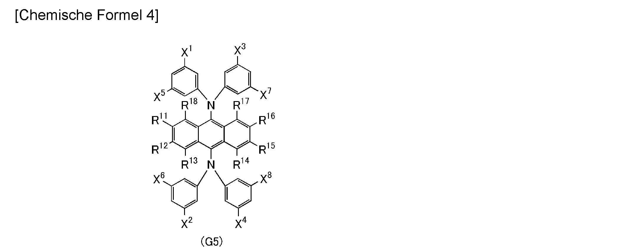
In der allgemeinen Formel (G5) stellen X1 bis X8 jeweils unabhängig voneinander eine verzweigtkettige Alkyl-Gruppe mit 3 bis 10 Kohlenstoffatomen, eine substituierte oder nicht substituierte Cycloalkyl-Gruppe mit 3 bis 10 Kohlenstoffatomen oder eine Trialkylsilyl-Gruppe mit 3 bis 10 Kohlenstoffatomen dar, und stellen R11 bis R18 jeweils unabhängig voneinander Wasserstoff, eine verzweigtkettige Alkyl-Gruppe mit 3 bis 10 Kohlenstoffatomen, eine substituierte oder nicht substituierte Cycloalkyl-Gruppe mit 3 bis 10 Kohlenstoffatomen, eine Trialkylsilyl-Gruppe mit 3 bis 10 Kohlenstoffatomen oder eine substituierte oder nicht substituierte Aryl-Gruppe mit 6 bis 25 Kohlenstoffatomen dar.In the general formula (G5), X 1 to X 8 each independently represent a branched-chain alkyl group having 3 to 10 carbon atoms, a substituted or unsubstituted cycloalkyl group having 3 to 10 carbon atoms or a trialkylsilyl group having 3 to 10 carbon atoms and R 11 to R 18 each independently represent hydrogen, a branched-chain alkyl group having 3 to 10 carbon atoms, a substituted or unsubstituted cycloalkyl group having 3 to 10 carbon atoms, a trialkylsilyl group having 3 to 10 carbon atoms or a substituted or unsubstituted aryl group having 6 to 25 carbon atoms.
Beispiele für eine Aryl-Gruppe mit 6 bis 25 Kohlenstoffatomen umfassen eine Phenyl-Gruppe, eine Naphthyl-Gruppe, eine Biphenyl-Gruppe, eine Fluorenyl-Gruppe und eine Spirofluorenyl-Gruppe. Es sei angemerkt, dass eine Aryl-Gruppe mit 6 bis 25 Kohlenstoffatomen nicht darauf beschränkt ist. In dem Fall, in dem die Aryl-Gruppe einen Substituenten aufweist, umfassen Beispiele für den Substituenten die Alkyl-Gruppe mit 1 bis 10 Kohlenstoffatomen, die verzweigtkettige Alkyl-Gruppe mit 3 bis 10 Kohlenstoffatomen, die substituierte oder nicht substituierte Cycloalkyl-Gruppe mit 3 bis 10 Kohlenstoffatomen und die Trialkylsilyl-Gruppe mit 3 bis 10 Kohlenstoffatomen, die vorstehend beschrieben worden sind.Examples of an aryl group having 6 to 25 carbon atoms include a phenyl group, a naphthyl group, a biphenyl group, a fluorenyl group and a spirofluorenyl group. Note that an aryl group having 6 to 25 carbon atoms is not limited to this. In the case where the aryl group has a substituent, examples of the substituent include the alkyl group having 1 to 10 carbon atoms, the branched chain alkyl group having 3 to 10 carbon atoms, the substituted or unsubstituted cycloalkyl group having 3 to 10 carbon atoms and the trialkylsilyl group of 3 to 10 carbon atoms described above.
Eine Anthracen-Verbindung weist eine hohe Emissionsquantenausbeute und eine kleine Fläche des Luminophors auf; deshalb können die oberen und unteren Flächen von Anthracen effizient mit den Schutzgruppen bedeckt werden. Ein Beispiel für die organische Verbindung, die durch die allgemeine Formel (G5) dargestellt wird, ist 2tBummtBuDPhA2Anth, das vorstehend beschrieben worden ist.An anthracene compound has a high emission quantum yield and a small area of the luminophore; therefore, the upper and lower surfaces of anthracene can be efficiently covered with the protective groups. An example of the organic compound represented by the general formula (G5) is 2tBummtBuDPhA2Anth, which has been described above.
Beispiele für die Verbindungen, die durch die allgemeinen Formeln (G1) bis (G5) dargestellt werden, werden durch die nachstehenden Strukturformeln (![]()


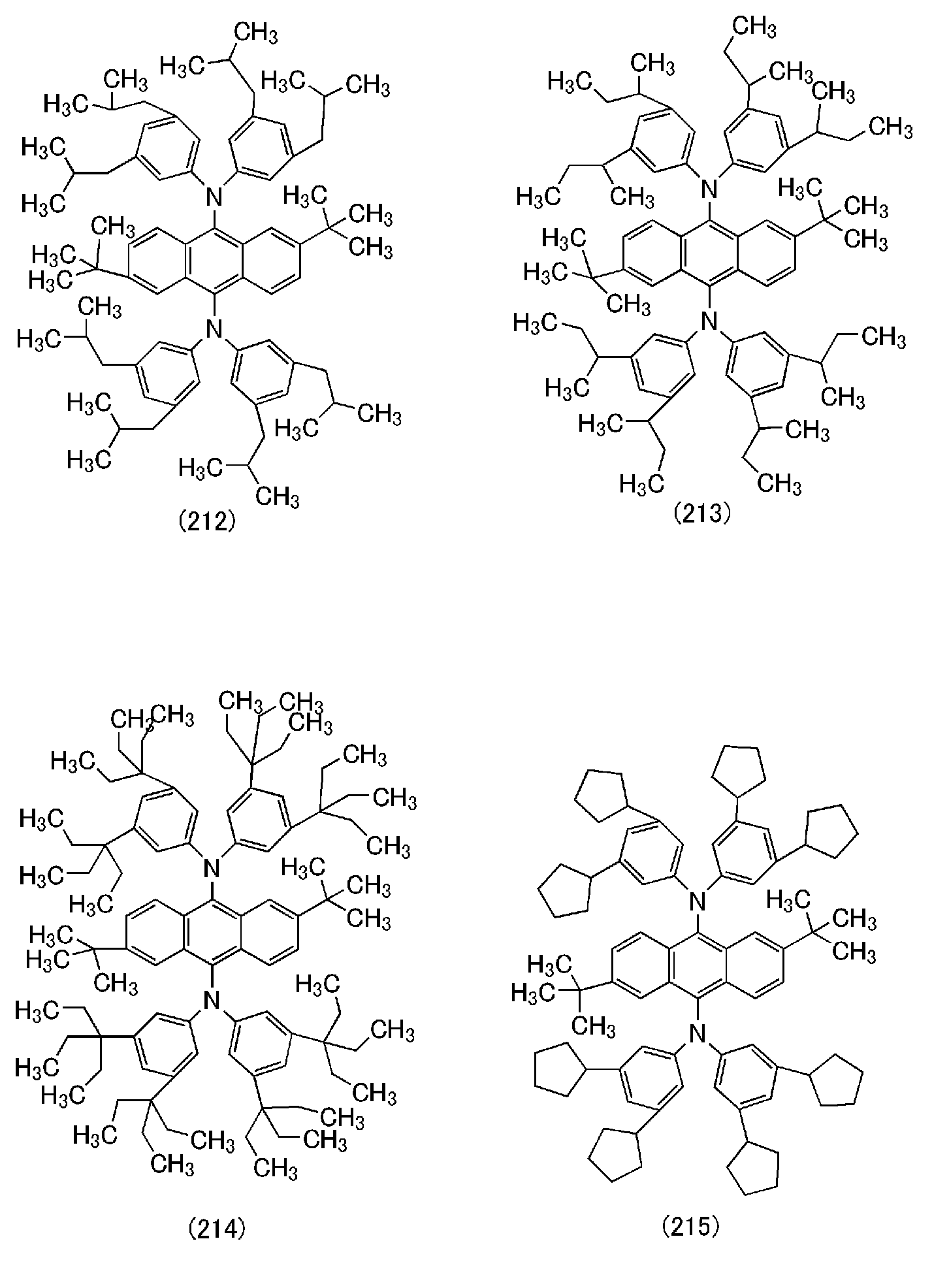


![]()

![]()

![]()

![]()


![]()

![]()

![]()


![]()


![]()
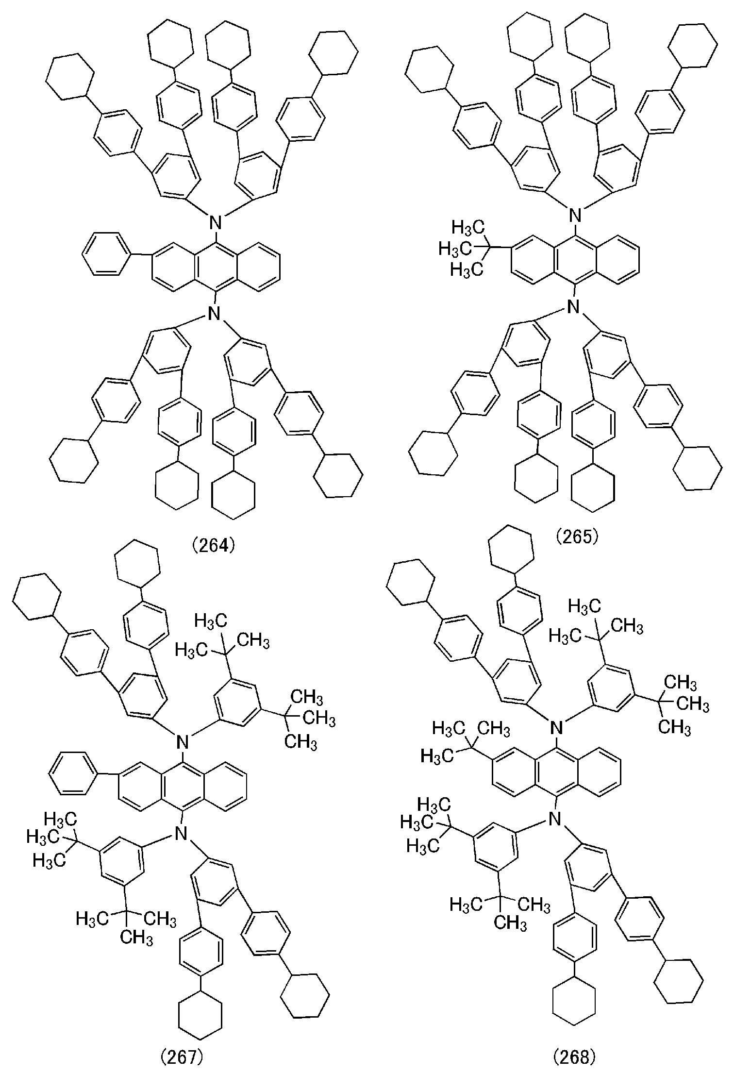
![]()

![]()

![]()


![]()
![]()
![]()
![]()
![]()
![]()
![]()
![]()
![]()
![]()
![]()
![]()
![]()
Beispiele für Materialien, die als Gastmaterial der Licht emittierenden Vorrichtung einer Ausführungsform der vorliegenden Erfindung vorteilhaft verwendet werden können, werden durch die Strukturformeln (
![]()
![]()

Wenn die Verbindung
Die Verbindung
In dem Fall, in dem das TADF-Material aus einer Materialart besteht, kann beispielsweise ein beliebiges der folgenden Materialien verwendet werden.In the case where the TADF material is made of one kind of material, for example, any of the following materials can be used.
Als Erstes können ein Fulleren, ein Derivat davon, ein Acridin-Derivat, wie z. B. Proflavin, Eosin und dergleichen aufgezählt werden. Weitere Beispiele umfassen ein metallhaltiges Porphyrin, wie z. B. ein Porphyrin, das Magnesium (Mg), Zink (Zn), Cadmium (Cd), Zinn (Sn), Platin (Pt), Indium (In) oder Palladium (Pd) enthält. Beispiele für das metallhaltige Porphyrin umfassen einen Protoporphyrin-Zinnfluorid-Komplex (SnF2(Proto IX)), einen Mesoporphyrin-Zinnfluorid-Komplex (SnF2(Meso IX)), einen Hämatoporphyrin-Zinnfluorid-Komplex (SnF2(Hämato IX)), einen Coproporphyrin-Tetramethylester-Zinnfluorid-Komplex (SnF2(Copro III-4Me)), einen Octaethylporphyrin-Zinnfluorid-Komplex (SnF2(OEP)), einen Etioporphyrin-Zinnfluorid-Komplex (SnF2(Etio I)) und einen Octaethylporphyrin-Platinchlorid-Komplex (PtCl2(OEP)).First, a fullerene, a derivative thereof, an acridine derivative such as e.g. B. Proflavin, Eosin and the like can be enumerated. Other examples include a metal-containing porphyrin, such as. B. a porphyrin containing magnesium (Mg), zinc (Zn), cadmium (Cd), tin (Sn), platinum (Pt), indium (In) or palladium (Pd). Examples of the metal-containing porphyrin include a protoporphyrin-tin fluoride complex (SnF 2 (Proto IX)), a mesoporphyrin-tin fluoride complex (SnF 2 (Meso IX)), a hematoporphyrin-tin fluoride complex (SnF 2 (Hemato IX)) , a coproporphyrin tetramethyl ester tin fluoride complex (SnF 2 (Copro III-4Me)), an octaethylporphyrin tin fluoride complex (SnF 2 (OEP)), an etioporphyrin tin fluoride complex (SnF 2 (Etio I)) and a Octaethylporphyrin platinum chloride complex (PtCl 2 (OEP)).


Als TADF-Material, das aus einer Materialart besteht, kann auch eine heterocyclische Verbindung, die ein π-elektronenreiches Gerüst und/oder ein π-elektronenarmes Gerüst aufweist, verwendet werden. Spezifische Beispiele umfassen 2-(Biphenyl-4-yl)-4,6-bis(12-phenylindolo[2,3-a]carbazol-11-yl)-1,3,5-triazin (Abkürzung: PIC-TRZ), 2-{4-[3-(N-Phenyl-9H-carbazol-3-yl)-9H-carbazol-9-yl]phenyl}-4,6-diphenyl-1,3,5-triazin (Abkürzung: PCCzPTzn), 2-[4-(10H-Phenoxazin-10-yl)phenyl]-4,6-diphenyl-1,3,5-triazin (Abkürzung: PXZ-TRZ), 3-[4-(5-Phenyl-5,10-dihydrophenazin-10-yl)phenyl]-4,5-diphenyl-1,2,4-triazol (Abkürzung: PPZ-3TPT), 3-(9,9-Dimethyl-9H-acridin-10-yl)-9H-xanthen-9-on (Abkürzung: ACRXTN), Bis[4-(9,9-dimethyl-9,10-dihydroacridin)phenyl]sulfon (Abkürzung: DMAC-DPS), 10-Phenyl-10H, 10'H-spiro[acridin-9,9'-anthracen]-10'-on (Abkürzung: ACRSA), 4-(9'-Phenyl-3,3'-bi-9H-carbazol-9-yl)benzofuro[3,2-d]pyrimidin (Abkürzung: 4PCCzBfpm), 4-[4-(9'-Phenyl-3,3'-bi-9H-carbazol-9-yl)phenyl]benzofuro[3,2-d]pyrimidin (Abkürzung: 4PCCzPBfpm) und 9-[3-(4,6-Diphenyl-1,3,5-triazin-2-yl)phenyl]-9'-phenyl-2,3'-bi-9H-carbazol (Abkürzung: mPCCzPTzn-02). Da die heterocyclische Verbindung das π-elektronenreiche Gerüst und das π-elektronenarme Gerüst aufweist, weist sie eine hohe Elektronentransporteigenschaft und eine hohe Lochtransporteigenschaft auf und wird daher bevorzugt. Unter Gerüsten mit dem π-elektronenarmen heteroaromatischen Ring werden ein Pyridin-Gerüst, ein Diazin-Gerüst (ein Pyrimidin-Gerüst, ein Pyrazin-Gerüst und ein Pyridazin-Gerüst) und ein Triazin-Gerüst aufgrund ihrer hohen Stabilität und hohen Zuverlässigkeit bevorzugt. Insbesondere werden ein Benzofuropyrimidin-Gerüst, ein Benzothienopyrimidin-Gerüst, ein Benzofuropyrazin-Gerüst und ein Benzothienopyrazin-Gerüst aufgrund ihrer hohen Akzeptoreigenschaften und hohen Zuverlässigkeit bevorzugt. Unter Gerüsten mit dem π-elektronenreichen heteroaromatischen Ring weisen ein Acridin-Gerüst, ein Phenoxazin-Gerüst, ein Phenothiazin-Gerüst, ein Furan-Gerüst, ein Thiophen-Gerüst und ein Pyrrol-Gerüst eine hohe Stabilität und eine hohe Zuverlässigkeit auf; demzufolge ist mindestens eines dieser Gerüste vorzugsweise enthalten. Als Furan-Gerüst wird ein Dibenzofuran-Gerüst bevorzugt. Als Thiophen-Gerüst wird ein Dibenzothiophen-Gerüst bevorzugt. Als Pyrrol-Gerüst werden insbesondere ein Indol-Gerüst, ein Carbazol-Gerüst, ein Bicarbazol-Gerüst und ein 3-(9-Phenyl-9H-carbazol-3-yl)-9H-carbazol-Gerüst bevorzugt. Es sei angemerkt, dass eine Substanz, in der ein π-elektronenreicher heteroaromatischer Ring direkt an einen π-elektronenarmen heteroaromatischen Ring gebunden ist, besonders bevorzugt verwendet wird, da sowohl die Donatoreigenschaft des π-elektronenreichen heteroaromatischen Rings als auch die Akzeptoreigenschaft des π-elektronenarmen heteroaromatischen Rings erhöht werden und die Differenz zwischen dem Niveau des Singulett-Anregungszustandes und dem Niveau des Triplett-Anregungszustandes klein wird. Es sei angemerkt, dass ein aromatischer Ring, an den eine elektronenziehende Gruppe, wie z. B. eine Cyano-Gruppe, gebunden ist, anstelle des π-elektronenarmen heteroaromatischen Rings verwendet werden kann.As the TADF material composed of one kind of material, a heterocyclic compound having a π-electron-rich skeleton and / or a π-electron-poor skeleton can also be used. Specific examples include 2- (biphenyl-4-yl) -4,6-bis (12-phenylindolo [2,3-a] carbazol-11-yl) -1,3,5-triazine (Abbreviation: PIC-TRZ) , 2- {4- [3- (N-phenyl-9H-carbazol-3-yl) -9H-carbazol-9-yl] phenyl} -4,6-diphenyl-1,3,5-triazine (abbreviation: PCCzPTzn), 2- [4- (10H-phenoxazin-10-yl) phenyl] -4,6-diphenyl-1,3,5-triazine (abbreviation: PXZ-TRZ), 3- [4- (5-phenyl -5,10-dihydrophenazin-10-yl) phenyl] -4,5-diphenyl-1,2,4-triazole (abbreviation: PPZ-3TPT), 3- (9,9-dimethyl-9H-acridine-10- yl) -9H-xanthen-9-one (abbreviation: ACRXTN), bis [4- (9,9-dimethyl-9,10-dihydroacridine) phenyl] sulfone (abbreviation: DMAC-DPS), 10-phenyl-10H, 10'H-spiro [acridin-9,9'-anthracene] -10'-one (abbreviation: ACRSA), 4- (9'-phenyl-3,3'-bi-9H-carbazol-9-yl) benzofuro [3,2-d] pyrimidine (abbreviation: 4PCCzBfpm), 4- [4- (9'-phenyl-3,3'-bi-9H-carbazol-9-yl) phenyl] benzofuro [3,2-d] pyrimidine (abbreviation: 4PCCzPBfpm) and 9- [3- (4,6-diphenyl-1,3,5-triazin-2-yl) phenyl] -9'-phenyl-2,3'-bi-9H-carbazole ( Abbreviation: mPCCzPTzn-02). Since the heterocyclic compound has the π-electron-rich skeleton and the π-electron-poor skeleton, it has a high electron transport property and a high hole transport property and is therefore preferred. Among the skeletons having the π-electron poor heteroaromatic ring, a pyridine skeleton, a diazine skeleton (a pyrimidine skeleton, a pyrazine skeleton and a pyridazine skeleton) and a triazine skeleton are preferred because of their high stability and high reliability. In particular, a benzofuropyrimidine skeleton, a benzothienopyrimidine skeleton, a benzofuropyrazine skeleton, and a benzothienopyrazine skeleton are preferred because of their high accepting properties and high reliability. Among skeletons with the π-electron-rich heteroaromatic ring, an acridine skeleton, a phenoxazine skeleton, a phenothiazine skeleton, a furan skeleton, a thiophene skeleton, and a pyrrole skeleton have high stability and high reliability; accordingly, at least one of these scaffolds is preferably included. A dibenzofuran structure is preferred as the furan structure. A dibenzothiophene structure is preferred as the thiophene structure. In particular, an indole structure, a carbazole structure, a bicarbazole structure are used as the pyrrole structure. Skeleton and a 3- (9-phenyl-9H-carbazol-3-yl) -9H-carbazole skeleton are preferred. It should be noted that a substance in which a π-electron-rich heteroaromatic ring is directly bonded to a π-electron-poor heteroaromatic ring is particularly preferably used because both the donor property of the π-electron-rich heteroaromatic ring and the acceptor property of the π-electron poor heteroaromatic ring can be increased and the difference between the level of the singlet excited state and the level of the triplet excited state becomes small. It should be noted that an aromatic ring to which an electron withdrawing group, such as. B. a cyano group, can be used instead of the π-electron-poor heteroaromatic ring.
![]()
![]()

In dem Fall, in dem die Verbindung
Beispiele für die Verbindung
Alternativ können beliebige der folgenden Lochtransportmaterialien und Elektronentransportmaterialien als Verbindung
Ein Material mit einer Eigenschaft zum Transportieren von mehr Löchern als Elektronen kann als Lochtransportmaterial verwendet werden, wobei ein Material mit einer Löcherbeweglichkeit von 1 × 10⁻⁶ cm2/Vs oder höher bevorzugt wird. Insbesondere kann ein aromatisches Amin, ein Carbazol-Derivat, ein aromatischer Kohlenwasserstoff, ein Stilben-Derivat oder dergleichen verwendet werden. Ferner kann es sich bei dem Lochtransportmaterial um eine hochmolekulare Verbindung handeln.A material having a property of transporting holes more than electrons can be used as the hole transporting material, with a material having a hole mobility of 1 × 10 -6 cm 2 / Vs or higher being preferred. In particular, an aromatic amine, a carbazole derivative, an aromatic hydrocarbon, a stilbene derivative or the like can be used. Furthermore, the hole transport material can be a high molecular compound.
Beispiele für das Material mit einer hohen Lochtransporteigenschaft umfassen aromatische Amin-Verbindungen, wie z. B. N,N'-Di(p-tolyl)-N,N'-diphenyl-p-phenylendiamin (Abkürzung: DTDPPA), 4,4'-Bis[N-(4-diphenylaminophenyl)-N-phenylamino]biphenyl (Abkürzung: DPAB), N,N'-Bis{4-[bis(3-methylphenyl)amino]phenyll-N,N'-diphenyl-(1,1'-biphenyl)-4,4'-diamin (Abkürzung: DNTPD) und 1,3,5-Tris[N-(4-diphenylaminophenyl)-N-phenylamino]benzol (Abkürzung: DPA3B).Examples of the material having a high hole transport property include aromatic amine compounds such as. B. N, N'-di (p-tolyl) -N, N'-diphenyl-p-phenylenediamine (abbreviation: DTDPPA), 4,4'-bis [N- (4-diphenylaminophenyl) -N-phenylamino] biphenyl (Abbreviation: DPAB), N, N'-Bis {4- [bis (3-methylphenyl) amino] phenyl-N, N'-diphenyl- (1,1'-biphenyl) -4,4'-diamine (abbreviation : DNTPD) and 1,3,5-tris [N- (4-diphenylaminophenyl) -N-phenylamino] benzene (abbreviation: DPA3B).
Spezifische Beispiele für das Carbazol-Derivat umfassen 3-[N-(4-Diphenylaminophenyl)-N-phenylamino]-9-phenylcarbazol (Abkürzung: PCzDPA1), 3,6-Bis[N-(4-diphenylaminophenyl)-N-phenylamino]-9-phenylcarbazol (Abkürzung: PCzDPA2), 3,6-Bis[N-(4-diphenylaminophenyl)-N-(1-naphthyl)amino]-9-phenylcarbazol (Abkürzung: PCzTPN2), 3-[N-(9-Phenylcarbazol-3-yl)-N-phenylamino]-9-phenylcarbazol (Abkürzung: PCzPCA1), 3,6-Bis[N-(9-phenylcarbazol-3-yl)-N-phenylamino]-9-phenylcarbazol (Abkürzung: PCzPCA2) und 3-[N-(1-Naphthyl)-N-(9-phenylcarbazol-3-yl)amino]-9-phenylcarbazol (Abkürzung: PCzPCN1).Specific examples of the carbazole derivative include 3- [N- (4-diphenylaminophenyl) -N-phenylamino] -9-phenylcarbazole (abbreviation: PCzDPA1), 3,6-bis [N- (4-diphenylaminophenyl) -N-phenylamino ] -9-phenylcarbazole (abbreviation: PCzDPA2), 3,6-bis [N- (4-diphenylaminophenyl) -N- (1-naphthyl) amino] -9-phenylcarbazole (abbreviation: PCzTPN2), 3- [N- ( 9-phenylcarbazol-3-yl) -N-phenylamino] -9-phenylcarbazole (abbreviation: PCzPCA1), 3,6-bis [N- (9-phenylcarbazol-3-yl) -N-phenylamino] -9-phenylcarbazole ( Abbreviation: PCzPCA2) and 3- [N- (1-naphthyl) -N- (9-phenylcarbazol-3-yl) amino] -9-phenylcarbazole (abbreviation: PCzPCN1).
Weitere Beispiele für das Carbazol-Derivat umfassen 4,4'-Di(N-carbazolyl)biphenyl (Abkürzung: CBP), 1,3,5-Tris[4-(N-carbazolyl)phenyl]benzol (Abkürzung: TCPB), 9-[4-(10-Phenyl-9-anthryl)phenyl]-9H-carbazol (Abkürzung: CzPA) und 1,4-Bis[4-(N-carbazolyl)phenyl]-2,3,5,6-tetraphenylbenzol.Further examples of the carbazole derivative include 4,4'-di (N-carbazolyl) biphenyl (abbreviation: CBP), 1,3,5-tris [4- (N-carbazolyl) phenyl] benzene (abbreviation: TCPB), 9- [4- (10-phenyl-9-anthryl) phenyl] -9H-carbazole (abbreviation: CzPA) and 1,4-bis [4- (N-carbazolyl) phenyl] -2,3,5,6- tetraphenylbenzene.
Beispiele für den aromatischen Kohlenwasserstoff umfassen 2-tert-Butyl-9,10-di(2-naphthyl)anthracen (Abkürzung: t-BuDNA), 2-tert-Butyl-9,10-di(1-naphthyl)anthracen, 9,10-Bis(3,5-diphenylphenyl)anthracen (Abkürzung: DPPA), 2-tert-Butyl-9,10-bis(4-phenylphenyl)anthracen (Abkürzung: t-BuDBA), 9,10-Di(2-naphthyl)anthracen (Abkürzung: DNA), 9,10-Diphenylanthracen (Abkürzung: DPAnth), 2-tert-Butylanthracen (Abkürzung: t-BuAnth), 9,10-Bis(4-methyl-1-naphthyl)anthracen (Abkürzung: DMNA), 2-tert-Butyl-9,10-bis[2-(1-naphthyl)phenyl]anthracen, 9,10-Bis[2-(1-naphthyl)phenyl]anthracen, 2,3,6,7-Tetramethyl-9,10-di(1-naphthyl)anthracen, 2,3,6,7-Tetramethyl-9,10-di(2-naphthyl)anthracen, 9,9'-Bianthryl, 10,10'-Diphenyl-9,9'-bianthryl, 10,10'-Bis(2-phenylphenyl)-9,9'-bianthryl, 10,10'-Bis[(2,3,4,5,6-pentaphenyl)phenyl]-9,9'bianthryl, Anthracen, Tetracen, Rubren, Perylen und 2,5,8,11-Tetra(tert-butyl)perylen. Weitere Beispiele umfassen Pentacen und Coronen. Der aromatische Kohlenwasserstoff, der eine Löcherbeweglichkeit von 1 × 10⁻⁶ cm2/Vs oder höher und 14 bis 42 Kohlenstoffatome aufweist, wird besonders bevorzugt.Examples of the aromatic hydrocarbon include 2-tert-butyl-9,10-di (2-naphthyl) anthracene (abbreviation: t-BuDNA), 2-tert-butyl-9,10-di (1-naphthyl) anthracene, 9 , 10-bis (3,5-diphenylphenyl) anthracene (abbreviation: DPPA), 2-tert-butyl-9,10-bis (4-phenylphenyl) anthracene (abbreviation: t-BuDBA), 9,10-di (2 -naphthyl) anthracene (abbreviation: DNA), 9,10-diphenylanthracene (abbreviation: DPAnth), 2-tert-butylanthracene (abbreviation: t-BuAnth), 9,10-bis (4-methyl-1-naphthyl) anthracene ( Abbreviation: DMNA), 2-tert-butyl-9,10-bis [2- (1-naphthyl) phenyl] anthracene, 9,10-bis [2- (1-naphthyl) phenyl] anthracene, 2,3,6 , 7-tetramethyl-9,10-di (1-naphthyl) anthracene, 2,3,6,7-tetramethyl-9,10-di (2-naphthyl) anthracene, 9,9'-bianthryl, 10,10 '-Diphenyl-9,9'-bianthryl,10,10'-bis (2-phenylphenyl) -9,9'-bianthryl, 10,10'-bis [(2,3,4,5,6-pentaphenyl) phenyl ] -9,9'bianthryl, anthracene, tetracene, rubrene, perylene and 2,5,8,11-tetra (tert-butyl) perylene. Other examples include pentacene and coronene. The aromatic hydrocarbon having a hole mobility of 1 × 10 -6 cm 2 / Vs or higher and 14 to 42 carbon atoms is particularly preferred.
Der aromatische Kohlenwasserstoff kann ein Vinyl-Gerüst aufweisen. Beispiele für den aromatischen Kohlenwasserstoff mit einer Vinyl-Gruppe umfassen 4,4'-Bis(2,2-diphenylvinyl)biphenyl (Abkürzung: DPVBi) und 9,10-Bis[4-(2,2-diphenylvinyl)phenyl]anthracen (Abkürzung: DPVPA).The aromatic hydrocarbon can have a vinyl backbone. Examples of the aromatic hydrocarbon having a vinyl group include 4,4'-bis (2,2-diphenylvinyl) biphenyl (abbreviation: DPVBi) and 9,10-bis [4- (2,2-diphenylvinyl) phenyl] anthracene ( Abbreviation: DPVPA).
Weitere Beispiele umfassen hochmolekulare Verbindungen, wie z. B. Poly(N-vinylcarbazol) (Abkürzung: PVK), Poly(4-vinyltriphenylamin) (Abkürzung: PVTPA), Poly[N-(4-{N'-[4-(4-diphenylamino)phenyl]phenyl-N-phenylamino}phenyl)methacrylamid] (Abkürzung: PTPDMA) und Poly[N,N'-bis(4-butylphenyl)-N,N'-bis(phenyl)benzidin] (Abkürzung: Poly-TPD).Other examples include high molecular weight compounds, such as. B. Poly (N-vinylcarbazole) (abbreviation: PVK), poly (4-vinyltriphenylamine) (abbreviation: PVTPA), poly [N- (4- {N '- [4- (4-diphenylamino) phenyl] phenyl] -N) -phenylamino} phenyl) methacrylamide] (abbreviation: PTPDMA) and poly [N, N'-bis (4-butylphenyl) -N, N'-bis (phenyl) benzidine] (abbreviation: Poly-TPD).
Beispiele für das Material mit einer hohen Lochtransporteigenschaft umfassen aromatische Amin-Verbindungen, wie z. B. 4,4'-Bis[N-(1-naphthyl)-N-phenylamino]biphenyl (Abkürzung: NPB oder α-NPD), N,N'-Bis(3-methylphenyl)-N,N'diphenyl-[1,1'-biphenyl]-4,4'-diamin (Abkürzung: TPD), 4,4',4"-Tris(carbazol-9-yl)triphenylamin (Abkürzung: TCTA), 4,4',4''-Tris[N-(1-naphthyl)-N-phenylamino]triphenylamin (Abkürzung: 1'-TNATA), 4,4',4"-Tris(N,N-diphenylamino)triphenylamin (Abkürzung: TDATA), 4,4',4"-Tris[N-(3-methylphenyl)-N-phenylamino]triphenylamin (Abkürzung: m-MTDATA), 4,4'-Bis[N-(spiro-9,9'-bifluoren-2-yl)-N-phenylamino]biphenyl (Abkürzung: BSPB), 4-Phenyl-4'-(9-phenylfluoren-9-yl)triphenylamin (Abkürzung: BPAFLP), 4-Phenyl-3'-(9-phenylfluoren-9-yl)triphenylamin (Abkürzung: mBPAFLP), N-(9,9-Dimethyl-9H-fluoren-2-yl)-N-{9,9-dimethyl-2-[N'-phenyl-N'-(9,9-dimethyl-9H-fluoren-2-yl)amino]-9H-fluoren-7-yl}phenylamin (Abkürzung: DFLADFL), N-(9,9-Dimethyl-2-diphenylamino-9H-fluoren-7-yl)diphenylamin (Abkürzung: DPNF), 2-[N-(4-Diphenylaminophenyl)-N-phenylamino]spiro-9,9'-bifluoren (Abkürzung: DPASF), 4-Phenyl-4'-(9-phenyl-9H-carbazol-3-yl)triphenylamin (Abkürzung: PCBA1BP), 4,4'-Diphenyl-4"-(9-phenyl-9H-carbazol-3-yl)triphenylamin (Abkürzung: PCBBi1BP), 4-(1-Naphthyl)-4'-(9-phenyl-9H-carbazol-3-yl)triphenylamin (Abkürzung: PCBANB), 4,4'-Di(1-naphthyl)-4"-(9-phenyl-9H-carbazol-3-yl)triphenylamin (Abkürzung: PCBNBB), 4-Phenyldiphenyl-(9-phenyl-9H-carbazol-3-yl)amin (Abkürzung: PCA1BP), N,N'-Bis(9-phenylcarbazol-3-yl)-N,N'-diphenylbenzol-1,3-diamin (Abkürzung: PCA2B), N,N',N''-Triphenyl-N,N',N''-tris(9-phenylcarbazol-3-yl)benzol-1,3,5-triamin (Abkürzung: PCA3B), N-(4-Biphenyl)-N-(9,9-Dimethyl-9H-fluoren-2-yl)-9-phenyl-9H-carbazol-3-amin (Abkürzung: PCBiF), N-(1,1'-Biphenyl-4-yl)-N-[4-(9-phenyl-9H-carbazol-3-yl)phenyl]-9,9-dimethyl-9H-fluoren-2-amin (Abkürzung: PCBBiF), 9,9-Dimethyl-N-phenyl-N-[4-(9-phenyl-9H-carbazol-3-yl)phenyl]fluoren-2-amin (Abkürzung: PCBAF), N-Phenyl-N-[4-(9-phenyl-9H-carbazol-3-yl)phenyl]spiro-9,9'-bifluoren-2-amin (Abkürzung: PCBASF), 2-[N-(9-Phenylcarbazol-3-yl)-N-phenylamino]spiro-9,9'-bifluoren (Abkürzung: PCASF), 2,7-Bis[N-(4-diphenylaminophenyl)-N-phenylamino]-spiro-9,9'-bifluoren (Abkürzung: DPA2SF), N-[4-(9H-Carbazol-9-yl)phenyl]-N-(4-phenyl)phenylanilin (Abkürzung: YGA1BP) und N,N'-Bis[4-(carbazol-9-yl)phenyl]-N,N'-diphenyl-9,9-dimethylfluoren-2,7-diamin (Abkürzung: YGA2F). Weitere Beispiele umfassen Amin-Verbindungen, Carbazol-Verbindungen, Thiophen-Verbindungen, Furan-Verbindungen, Fluoren-Verbindungen, Triphenylen-Verbindungen, Phenanthren-Verbindungen und dergleichen, wie z. B. 3-[4-(1-Naphthyl)-phenyl]-9-phenyl-9H-carbazol (Abkürzung: PCPN), 3-[4-(9-Phenanthryl)-phenyl]-9-phenyl-9H-carbazol (Abkürzung: PCPPn), 3,3'-Bis(9-phenyl-9H-carbazol) (Abkürzung: PCCP), 1,3-Bis(N-carbazolyl)benzol (Abkürzung: mCP), 3,6-Bis(3,5-diphenylphenyl)-9-phenylcarbazol (Abkürzung: CzTP), 4-{3-[3-(9-Phenyl-9H-fluoren-9-yl)phenyl]phenyl}dibenzofuran (Abkürzung: mmDBFFLBi-II), 4,4',4"-(Benzol-1,3,5-triyl)tri(dibenzofuran) (Abkürzung: DBF3P-II), 1,3,5-Tri(dibenzothiophen-4-yl)-benzol (Abkürzung: DBT3P-II), 2,8-Diphenyl-4-[4-(9-phenyl-9H-fluoren-9-yl)phenyl]dibenzothiophen (Abkürzung: DBTFLP-III), 4-[4-(9-Phenyl-9H-fluoren-9-yl)phenyl]-6-phenyldibenzothiophen (Abkürzung: DBTFLP-IV) und 4-[3-(Triphenylen-2-yl)phenyl]dibenzothiophen (Abkürzung: mDBTPTp-II). Die hier beschriebenen Substanzen sind hauptsächlich Substanzen mit einer Löcherbeweglichkeit von 1 × 10⁻⁶ cm2/Vs oder höher. Es sei angemerkt, dass außer diesen Substanzen eine beliebige Substanz verwendet werden kann, die eine Eigenschaft zum Transportieren von mehr Löchern als Elektronen aufweist.Examples of the material having a high hole transport property include aromatic amine compounds such as. B. 4,4'-bis [N- (1-naphthyl) -N-phenylamino] biphenyl (abbreviation: NPB or α-NPD), N, N'-bis (3-methylphenyl) -N, N'diphenyl- [1,1'-biphenyl] -4,4'-diamine (abbreviation: TPD), 4,4 ', 4 "-Tris (carbazol-9-yl) triphenylamine (abbreviation: TCTA), 4,4', 4 '' -Tris [N- (1-naphthyl) -N-phenylamino] triphenylamine (abbreviation: 1'-TNATA), 4,4 ', 4 "-Tris (N, N-diphenylamino) triphenylamine (abbreviation: TDATA), 4,4 ', 4 "-Tris [N- (3-methylphenyl) -N-phenylamino] triphenylamine (abbreviation: m-MTDATA), 4,4'-bis [N- (spiro-9,9'-bifluorene- 2-yl) -N-phenylamino] biphenyl (abbreviation: BSPB), 4-phenyl-4 '- (9-phenylfluoren-9-yl) triphenylamine (abbreviation: BPAFLP), 4-phenyl-3 '- (9-phenylfluoren-9-yl) triphenylamine (abbreviation: mBPAFLP), N- (9,9-dimethyl-9H-fluoren-2-yl) -N- {9,9-dimethyl- 2- [N'-phenyl-N '- (9,9-dimethyl-9H-fluoren-2-yl) amino] -9H-fluoren-7-yl} phenylamine (abbreviation: DFLADFL), N- (9.9 -Dimethyl-2-diphenylamino-9H-fluoren-7-yl) diphenylamine (abbreviation: DPNF), 2- [N- (4-diphenylaminophenyl) -N-phenylamino] spiro-9,9'-bifluorene (abbreviation: DPASF) , 4-phenyl-4 '- (9-phenyl-9H-carbazol-3-yl) triphenylamine (abbreviation: PCBA1BP), 4,4'-diphenyl-4 "- (9-phenyl-9H-carbazol-3-yl ) triphenylamine (abbreviation: PCBBi1BP), 4- (1-naphthyl) -4 '- (9-phenyl-9H-carbazol-3-yl) triphenylamine (abbreviation: PCBANB), 4,4'-di (1-naphthyl) -4 "- (9-phenyl-9H-carbazol-3-yl) triphenylamine (abbreviation: PCBNBB), 4-phenyldiphenyl- (9-phenyl-9H-carbazol-3-yl) amine (abbreviation: PCA1BP), N, N'-bis (9-phenylcarbazol-3-yl) -N, N'-diphenylbenzene-1,3-diamine (abbreviation: PCA2B), N, N ', N''- triphenyl-N, N', N ''-tris (9-phenylcarbazol-3-yl) benzene-1,3,5-triamine (abbreviation: PCA3B), N- (4-biphenyl) -N- (9,9-dimethyl-9H-fluorene-2- y l) -9-phenyl-9H-carbazol-3-amine (abbreviation: PCBiF), N- (1,1'-biphenyl-4-yl) -N- [4- (9-phenyl-9H-carbazol-3 -yl) phenyl] -9,9-dimethyl-9H-fluoren-2-amine (abbreviation: PCBBiF), 9,9-dimethyl-N-phenyl-N- [4- (9-phenyl-9H-carbazole-3 -yl) phenyl] fluoren-2-amine (abbreviation: PCBAF), N-phenyl-N- [4- (9-phenyl-9H-carbazol-3-yl) phenyl] spiro-9,9'-bifluorene-2 -amine (abbreviation: PCBASF), 2- [N- (9-phenylcarbazol-3-yl) -N-phenylamino] spiro-9,9'-bifluorene (abbreviation: PCASF), 2,7-bis [N- ( 4-diphenylaminophenyl) -N-phenylamino] -spiro-9,9'-bifluorene (abbreviation: DPA2SF), N- [4- (9H-carbazol-9-yl) phenyl] -N- (4-phenyl) phenylaniline ( Abbreviation: YGA1BP) and N, N'-bis [4- (carbazol-9-yl) phenyl] -N, N'-diphenyl-9,9-dimethylfluorene-2,7-diamine (abbreviation: YGA2F). Further examples include amine compounds, carbazole compounds, thiophene compounds, furan compounds, fluorene compounds, triphenylene compounds, phenanthrene compounds and the like, such as. B. 3- [4- (1-Naphthyl) -phenyl] -9-phenyl-9H-carbazole (abbreviation: PCPN), 3- [4- (9-phenanthryl) -phenyl] -9-phenyl-9H-carbazole (Abbreviation: PCPPn), 3,3'-bis (9-phenyl-9H-carbazole) (abbreviation: PCCP), 1,3-bis (N-carbazolyl) benzene (abbreviation: mCP), 3,6-bis ( 3,5-diphenylphenyl) -9-phenylcarbazole (abbreviation: CzTP), 4- {3- [3- (9-phenyl-9H-fluoren-9-yl) phenyl] phenyl} dibenzofuran (abbreviation: mmDBFFLBi-II), 4,4 ', 4 "- (benzene-1,3,5-triyl) tri (dibenzofuran) (abbreviation: DBF3P-II), 1,3,5-tri (dibenzothiophen-4-yl) -benzene (abbreviation: DBT3P-II), 2,8-diphenyl-4- [4- (9-phenyl-9H-fluoren-9-yl) phenyl] dibenzothiophene (abbreviation: DBTFLP-III), 4- [4- (9-phenyl- 9H-fluoren-9-yl) phenyl] -6-phenyldibenzothiophene (abbreviation: DBTFLP-IV) and 4- [3- (triphenylen-2-yl) phenyl] dibenzothiophene (abbreviation: mDBTPTp-II). The substances described here are mainly substances with a hole mobility of 1 × 10 -6 cm 2 / Vs or higher. It should be noted that any substance other than these substances can be used which can ei ne property to transport more holes than electrons.
Ein Material mit einer Eigenschaft zum Transportieren von mehr Elektronen als Löchern kann als Elektronentransportmaterial verwendet werden, wobei ein Material mit einer Elektronenbeweglichkeit von 1 × 10⁻⁶ cm2/Vs oder höher bevorzugt wird. Als Material, das leicht Elektronen aufnimmt (Material mit einer Elektronentransporteigenschaft), kann eine π-elektronenarme heteroaromatische Verbindung, wie z. B. eine stickstoffhaltige heteroaromatische Verbindung, ein Metallkomplex oder dergleichen verwendet werden. Spezifische Beispiele umfassen einen Metallkomplex mit einem Chinolin-Liganden, einem Benzochinolin-Liganden, einem Oxazol-Liganden oder einem Thiazol-Liganden, ein Oxadiazol-Derivat, ein Triazol-Derivat, ein Phenanthrolin-Derivat, ein Pyridin-Derivat, ein Bipyridin-Derivat und ein Pyrimidin-Derivat.A material having a property of transporting more electrons than holes can be used as the electron transporting material, with a material having an electron mobility of 1 × 10 -6 cm 2 / Vs or higher being preferred. As a material easily accepting electrons (material having an electron transport property), a π-electron-poor heteroaromatic compound such as. B. a nitrogen-containing heteroaromatic compound, a metal complex or the like can be used. Specific examples include a metal complex having a quinoline ligand, a benzoquinoline ligand, an oxazole ligand or a thiazole ligand, an oxadiazole derivative, a triazole derivative, a phenanthroline derivative, a pyridine derivative, a bipyridine derivative and a pyrimidine derivative.
Beispiele für das Elektronentransportmaterial umfassen Metallkomplexe mit einem Chinolin-Gerüst oder einem Benzochinolin-Gerüst, wie z. B. Tris(8-chinolinolato)aluminium(III) (Abkürzung: Alq), Tris(4-methyl-8-chinolinolato)aluminium(III) (Abkürzung: Almq3), Bis(10-hydroxybenzo[h]chinolinato)beryllium(II) (Abkürzung: BeBq2), Bis(2-methyl-8-chinolinolato)(4-phenylphenolato)aluminium(III) (Abkürzung: BAIq) und Bis(8-chinolinolato)zink(II) (Abkürzung: Znq). Alternativ kann ein Metallkomplex mit einem Liganden auf Oxazol-Basis oder einem Liganden auf Thiazol-Basis, wie z. B. Bis[2-(2-benzoxazolyl)phenolato]zink(II) (Abkürzung: ZnPBO) oder Bis[2-(2-benzothiazolyl)phenolato]zink(II) (Abkürzung: ZnBTZ), verwendet werden. Neben derartigen Metallkomplexen können beliebige der Folgenden verwendet werden: heterocyclische Verbindungen, wie z. B. 2-(4-Biphenylyl)-5-(4-tert-butylphenyl)-1,3,4-oxadiazol (Abkürzung: PBD), 1,3-Bis[5-(p-tert-butylphenyl)-1,3,4-oxadiazol-2-yl]benzol (Abkürzung: OXD-7), 9-[4-(5-Phenyl-1,3,4-oxadiazol-2-yl)phenyl]-9H-carbazol (Abkürzung: CO11), 3-(4-Biphenylyl)-4-phenyl-5-(4-tert-butylphenyl)-1,2,4-triazol (Abkürzung: TAZ), 2,2',2"-(1,3,5-Benzoltriyl)tris(1-phenyl-1H-benzimidazol) (Abkürzung: TPBI), 2-[3-(Dibenzothiophen-4-yl)phenyl]-1-phenyl-1 H-benzimidazol (Abkürzung: mDBTBIm-II), Bathophenanthrolin (Abkürzung: BPhen), 2,9-Bis(naphthalen-2-yl)-4,7-diphenyl-1,10-phenanthrolin (Abkürzung: NBPhen) und Bathocuproin (Abkürzung: BCP), heterocyclische Verbindungen mit einem Diazin-Gerüst, wie z. B. 2-[3-(Dibenzothiophen-4-yl)phenyl]dibenzo[f,h]chinoxalin (Abkürzung: 2mDBTPDBq-II), 2-[3'-(Dibenzothiophen-4-yl)biphenyl-3-yl]dibenzo[f,h]chinoxalin (Abkürzung: 2mDBTBPDBq-II), 2-[3'-(9H-Carbazol-9-yl)biphenyl-3-yl]dibenzo[f,h]chinoxalin (Abkürzung: 2mCzBPDBq), 2-[4-(3,6-Diphenyl-9H-carbazol-9-yl)phenyl]dibenzo[f,h]chinoxalin (Abkürzung: 2CzPDBq-III), 7-[3-(Dibenzothiophen-4-yl)phenyl]dibenzo[f,h]chinoxalin (Abkürzung: 7mDBTPDBq-II), 6-[3-(Dibenzothiophen-4-yl)phenyl]dibenzo[f,h]chinoxalin (Abkürzung: 6mDBTPDBq-II), 4,6-Bis[3-(phenanthren-9-yl)phenyl]pyrimidin (Abkürzung: 4,6mPnP2Pm), 4,6-Bis[3-(4-dibenzothienyl)phenyl]pyrimidin (Abkürzung: 4,6mDBTP2Pm-II) und 4,6-Bis[3-(9H-carbazol-9-yl)phenyl]pyrimidin (Abkürzung: 4,6mCzP2Pm), heterocyclische Verbindungen mit einem Triazin-Gerüst, wie z. B. 2-{4-[3-(/V-Phenyl-9H-carbazol-3-yl)-9H-carbazol-9-yl]phenyl}-4,6-diphenyl-1,3,5-triazin (Abkürzung: PCCzPTzn), heterocyclische Verbindungen mit einem Pyridin-Gerüst, wie z. B. 3,5-Bis[3-(9H-carbazol-9-yl)phenyl]pyridin (Abkürzung: 35DCzPPy) und 1,3,5-Tri[3-(3-pyridyl)phenyl]benzol (Abkürzung: TmPyPB), und heteroaromatische Verbindungen, wie z. B. 4,4'-Bis(5-methylbenzoxazol-2-yl)stilben (Abkürzung: BzOs). Als weitere Alternative kann eine hochmolekulare Verbindung, wie z. B. Poly(2,5-pyridindiyl) (Abkürzung: PPy), Poly[(9,9-dihexylfluoren-2,7-diyl)-co-(pyridin-3,5-diyl)] (Abkürzung: PF-Py) oder Poly[(9,9-dioctylfluoren-2,7-diyl)-co-(2,2'-bipyridin-6,6'-diyl)] (Abkürzung: PF-BPy), verwendet werden. Die hier beschriebenen Substanzen sind hauptsächlich Substanzen mit einer Elektronenbeweglichkeit von 1 x 10⁻⁶ cm2/Vs oder höher. Es sei angemerkt, dass außer diesen Substanzen eine beliebige Substanz verwendet werden kann, die eine Eigenschaft zum Transportieren von mehr Elektronen als Löchern aufweist.Examples of the electron transport material include metal complexes having a quinoline skeleton or a benzoquinoline skeleton, such as. B. Tris (8-quinolinolato) aluminum (III) (abbreviation: Alq), tris (4-methyl-8-quinolinolato) aluminum (III) (abbreviation: Almq 3 ), bis (10-hydroxybenzo [h] quinolinato) beryllium (II) (abbreviation: BeBq 2 ), bis (2-methyl-8-quinolinolato) (4-phenylphenolato) aluminum (III) (abbreviation: BAIq) and bis (8-quinolinolato) zinc (II) (abbreviation: Znq) . Alternatively, a metal complex with an oxazole-based ligand or a thiazole-based ligand, such as e.g. B. bis [2- (2-benzoxazolyl) phenolato] zinc (II) (abbreviation: ZnPBO) or bis [2- (2-benzothiazolyl) phenolato] zinc (II) (abbreviation: ZnBTZ) can be used. In addition to such metal complexes, any of the following can be used: heterocyclic compounds such as. B. 2- (4-biphenylyl) -5- (4-tert-butylphenyl) -1,3,4-oxadiazole (abbreviation: PBD), 1,3-bis [5- (p-tert-butylphenyl) -1 , 3,4-oxadiazol-2-yl] benzene (abbreviation: OXD-7), 9- [4- (5-phenyl-1,3,4-oxadiazol-2-yl) phenyl] -9H-carbazole (abbreviation : CO11), 3- (4-biphenylyl) -4-phenyl-5- (4-tert-butylphenyl) -1,2,4-triazole (abbreviation: TAZ), 2,2 ', 2 "- (1, 3,5-Benzoltriyl) tris (1-phenyl-1H-benzimidazole) (Abbreviation: TPBI), 2- [3- (Dibenzothiophen-4-yl) phenyl] -1-phenyl-1 H-benzimidazole (Abbreviation: mDBTBIm- II), bathophenanthroline (abbreviation: BPhen), 2,9-bis (naphthalen-2-yl) -4,7-diphenyl-1,10-phenanthroline (abbreviation: NBPhen) and bathocuproin (abbreviation: BCP), heterocyclic compounds with a diazine structure, such as, for example, 2- [3- (dibenzothiophen-4-yl) phenyl] dibenzo [f, h] quinoxaline (abbreviation: 2mDBTPDBq-II), 2- [3 '- (dibenzothiophen-4- yl) biphenyl-3-yl] dibenzo [f, h] quinoxaline (abbreviation: 2mDBTBPDBq-II), 2- [3 '- (9H-carbazol-9-yl) biphenyl-3-yl] dibenzo [f, h] quinoxaline (abbreviation: 2mCzBPDBq), 2- [4- (3,6-diphenyl-9H-carbazol-9-yl) phenyl] diben zo [f, h] quinoxaline (abbreviation: 2CzPDBq-III), 7- [3- (dibenzothiophen-4-yl) phenyl] dibenzo [f, h] quinoxaline (abbreviation: 7mDBTPDBq-II), 6- [3- ( Dibenzothiophen-4-yl) phenyl] dibenzo [f, h] quinoxaline (abbreviation: 6mDBTPDBq-II), 4,6-bis [3- (phenanthren-9-yl) phenyl] pyrimidine (abbreviation: 4,6mPnP2Pm), 4,6-bis [3- (4-dibenzothienyl) phenyl] pyrimidine (abbreviation: 4,6mDBTP2Pm-II) and 4,6-bis [3- (9H-carbazol-9-yl) phenyl] pyrimidine (abbreviation: 4,6mCzP2Pm), heterocyclic compounds with a triazine structure, such as B. 2- {4- [3 - (/ V-phenyl-9H-carbazol-3-yl) -9H-carbazol-9-yl] phenyl} -4,6-diphenyl-1,3,5-triazine ( Abbreviation: PCCzPTzn), heterocyclic compounds with a pyridine structure, such as B. 3,5-bis [3- (9H-carbazol-9-yl) phenyl] pyridine (abbreviation: 35DCzPPy) and 1,3,5-tri [3- (3-pyridyl) phenyl] benzene (abbreviation: TmPyPB ), and heteroaromatic compounds, such as. B. 4,4'-bis (5-methylbenzoxazol-2-yl) stilbene (abbreviation: BzOs). As a further alternative, a high molecular weight compound, such as. B. Poly (2,5-pyridinediyl) (abbreviation: PPy), poly [(9,9-dihexylfluoren-2,7-diyl) -co- (pyridin-3,5-diyl)] (abbreviation: PF-Py ) or poly [(9,9-dioctylfluoren-2,7-diyl) -co- (2,2'-bipyridin-6,6'-diyl)] (abbreviation: PF-BPy) can be used. The substances described here are mainly substances with an electron mobility of 1 × 10 -6 cm 2 / Vs or higher. Note that, besides these substances, any substance having a property of transporting more electrons than holes can be used.
Als Verbindung
Als Verbindung
Beispiele für eine Substanz, die einen Emissionspeak im blauen oder grünen Wellenlängenbereich aufweist, umfassen metallorganische Iridiumkomplexe mit einem 4H-Triazol-Gerüst, wie z. B. Trisf2-[5-(2-methylphenyl)-4-(2,6-dimethylphenyl)-4H-1,2,4-triazol-3-yl-κN2]phenyl-κC}iridium(111) (Abkürzung: Ir(mpptz-dmp)3), Tris(5-methyl-3,4-diphenyl-4H-1,2,4-triazolato)iridium(III) (Abkürzung: Ir(Mptz)3), Tris[4-(3-biphenyl)-5-isopropyl-3-phenyl-4H-1,2,4-triazolato]iridium(III) (Abkürzung: Ir(iPrptz-3b)3) und Tris[3-(5-biphenyl)-5-isopropyl-4-phenyl-4H-1,2,4-triazolato]iridium(III) (Abkürzung: Ir(iPr5btz)3), metallorganische Iridiumkomplexe mit einem 1H-Triazol-Gerüst, wie z. B. Tris[3-methyl-1-(2-methylphenyl)-5-phenyl-1H-1,2,4-triazolato]iridium(III) (Abkürzung: Ir(Mptz1-mp)3) und Tris(1-methyl-5-phenyl-3-propyl-1H-1,2,4-triazolato)iridium(III) (Abkürzung: Ir(Prptz1-Me)3), metallorganische Iridiumkomplexe mit einem Imidazol-Gerüst, wie z. B. fac-Tris[1-(2,6-diisopropylphenyl)-2-phenyl-1H-imidazol]iridium(III) (Abkürzung: Ir(iPrpmi)3) und Tris[3-(2,6-dimethylphenyl)-7-methylimidazo[1,2-f]phenanthridinato]iridium(III) (Abkürzung: Ir(dmpimpt-Me)3), und metallorganische Iridiumkomplexe, bei denen ein Phenylpyridin-Derivat mit einer elektronenziehenden Gruppe ein Ligand ist, wie z. B. Bis[2-(4',6'-difluorphenyl)pyridinato-N,C2']iridium(III)tetrakis(1-pyrazolyl)borat (Abkürzung: Fir6), Bis[2-(4',6'difluorphenyl)pyridinato-N,C2']iridium(III)picolinat (Abkürzung: Firpic), Bis{2-[3',5'bis(trifluormethyl)phenyl]pyridinato-N,C2}iridium(III)picolinat (Abkürzung: Ir(CF3ppy)2(pic)) und Bis[2-(4',6'-difluorphenyl)pyridinato-N,C2']iridium(III)acetylacetonat (Abkürzung: Fir(acac)). Unter den vorstehend angegebenen Materialien weisen die metallorganischen Iridiumkomplexe, die ein fünfgliedriges stickstoffhaltiges heteroaromatisches Ringgerüst, wie z. B. ein 4H-Triazol-Gerüst, ein 1H-Triazol-Gerüst oder ein Imidazol-Gerüst, aufweisen, eine hohe Triplett-Anregungsenergie, Zuverlässigkeit und Lichtausbeute auf und werden daher besonders bevorzugt.Examples of a substance which has an emission peak in the blue or green wavelength range include organometallic iridium complexes with a 4H-triazole skeleton, such as. B. Trisf2- [5- (2-methylphenyl) -4- (2,6-dimethylphenyl) -4H-1,2,4-triazol-3-yl-κN 2 ] phenyl-κC} iridium (111) (abbreviation : Ir (mpptz-dmp) 3 ), Tris (5-methyl-3,4-diphenyl-4H-1,2,4-triazolato) iridium (III) (abbreviation: Ir (Mptz) 3 ), Tris [4- (3-biphenyl) -5-isopropyl-3-phenyl-4H-1,2,4-triazolato] iridium (III) (abbreviation: Ir (iPrptz-3b) 3 ) and tris [3- (5-biphenyl) - 5-isopropyl-4-phenyl-4H-1,2,4-triazolato] iridium (III) (abbreviation: Ir (iPr5btz) 3 ), organometallic iridium complexes with a 1H-triazole structure, such as. B. Tris [3-methyl-1- (2-methylphenyl) -5-phenyl-1H-1,2,4-triazolato] iridium (III) (abbreviation: Ir (Mptz1-mp) 3 ) and Tris (1- methyl-5-phenyl-3-propyl-1H-1,2,4-triazolato) iridium (III) (abbreviation: Ir (Prptz1-Me) 3 ), organometallic iridium complexes with an imidazole structure, such as. B. fac-Tris [1- (2,6-diisopropylphenyl) -2-phenyl-1H-imidazole] iridium (III) (abbreviation: Ir (iPrpmi) 3 ) and Tris [3- (2,6-dimethylphenyl) - 7-methylimidazo [1,2-f] phenanthridinato] iridium (III) (abbreviation: Ir (dmpimpt-Me) 3 ), and organometallic iridium complexes in which a phenylpyridine derivative with an electron-withdrawing group is a ligand, e.g. B. Bis [2- (4 ', 6'-difluorophenyl) pyridinato-N, C 2 '] iridium (III) tetrakis (1-pyrazolyl) borate (abbreviation: Fir6), bis [2- (4 ', 6' difluorophenyl) pyridinato-N, C 2 '] iridium (III) picolinate (abbreviation: Firpic), bis {2- [3', 5'bis (trifluoromethyl) phenyl] pyridinato-N, C 2 } iridium (III) picolinate ( Abbreviation: Ir (CF 3 ppy) 2 (pic)) and bis [2- (4 ', 6'-difluorophenyl) pyridinato-N, C 2 '] iridium (III) acetylacetonate (abbreviation: Fir (acac)). Among the materials given above, the organometallic iridium complexes that have a five-membered nitrogen-containing heteroaromatic ring structure, such as. B. a 4H-triazole structure, a 1H-triazole structure or an imidazole structure, have a high triplet excitation energy, reliability and light yield and are therefore particularly preferred.
Beispiele für eine Substanz, die einen Emissionspeak im grünen oder gelben Wellenlängenbereich aufweist, umfassen metallorganische Iridiumkomplexe mit einem Pyrimidin-Gerüst, wie z. B. Tris(4-methyl-6-phenylpyrimidinato)iridium(III) (Abkürzung: Ir(mppm)3), Tris(4-t-butyl-6-phenylpyrimidinato)iridium(III) (Abkürzung: Ir(tBuppm)3), (Acetylacetonato)bis(6-methyl-4-phenylpyrimidinato)iridium(III) (Abkürzung: Ir(mppm)2(acac)), (Acetylacetonato)bis(6-tert-butyl-4-phenylpyrimidinato)iridium(III) (Abkürzung: Ir(tBuppm)2(acac)), (Acetylacetonato)bis[4-(2-norbornyl)-6-phenylpyrimidinato]iridium(III) (Abkürzung: Ir(nbppm)2(acac)), (Acetylacetonato)bis[5-methyl-6-(2-methylphenyl)-4-phenylpyrimidinato]iridium(III) (Abkürzung: lr(mpmppm)2(acac)), (Acetylacetonato)bis{4,6-dimethyl-2-[6-(2,6-dimethylphenyl)-4-pyrimidinyl-κA/3]phenyl-κC}iridium(lll) (Abkürzung: Ir(dmppm-dmp)2(acac)) und (Acetylacetonato)bis(4,6-diphenylpyrimidinato)iridium(III) (Abkürzung: Ir(dppm)2(acac)), metallorganische Iridiumkomplexe mit einem Pyrazin-Gerüst, wie z. B. (Acetylacetonato)bis(3,5-dimethyl-2-phenylpyrazinato)iridium(III) (Abkürzung: Ir(mppr-Me)2(acac)) und (Acetylacetonato)bis(5-isopropyl-3-methyl-2-phenylpyrazinato)iridium(III) (Abkürzung: Ir(mppr-iPr)2(acac)), metallorganische Iridiumkomplexe mit einem Pyridin-Gerüst, wie z. B. Tris(2-phenylpyridinato-N, C2')iridium(III) (Abkürzung: Ir(ppy)3), Bis(2-phenylpyridinato-N,C2')iridium(III)acetylacetonat (Abkürzung: Ir(ppy)2(acac)), Bis(benzo[h]chinolinato)iridium(III)acetylacetonat (Abkürzung: Ir(bzq)2(acac)), Tris(benzo[h]chinolinato)iridium(III) (Abkürzung: Ir(bzq)3), Tris(2-phenylchinolinato-N, C2')iridium(III) (Abkürzung: Ir(pq)3) und Bis(2-phenylchinolinato-N,C2')iridium(111)acetylacetonat (Abkürzung: Ir(pq)2(acac)), metallorganische Iridiumkomplexe, wie z. B. Bis(2,4-diphenyl-1,3-oxazolato-N,C2')iridium(III)acetylacetonat (Abkürzung: Ir(dpo)2(acac)), Bis{2-[4'-(perfluorphenyl)phenyl]pyridinato-N,C2'}iridium(III)acetylacetonat (Abkürzung: Ir(p-PF-ph)2(acac)) und Bis(2-phenylbenzothiazolato-N,C2')iridium(III)acetylacetonat (Abkürzung: Ir(bt)2(acac)), und einen Seltenerdmetallkomplex, wie z. B. Tris(acetylacetonato)(monophenanthrolin)terbium(III) (Abkürzung: Tb(acac)3(Phen)). Unter den vorstehend angegebenen Materialien weisen die metallorganischen Iridiumkomplexe mit einem Pyrimidin-Gerüst eine deutlich hohe Zuverlässigkeit und Lichtausbeute auf und werden daher besonders bevorzugt.Examples of a substance which has an emission peak in the green or yellow wavelength range include organometallic iridium complexes with a pyrimidine skeleton, such as. B. Tris (4-methyl-6-phenylpyrimidinato) iridium (III) (Abbreviation: Ir (mppm) 3 ), Tris (4-t-butyl-6-phenylpyrimidinato) iridium (III) (Abbreviation: Ir (tBuppm) 3 ), (Acetylacetonato) bis (6-methyl-4-phenylpyrimidinato) iridium (III) (Abbreviation: Ir (mppm) 2 (acac)), (Acetylacetonato) bis (6-tert-butyl-4-phenylpyrimidinato) iridium (III ) (Abbreviation: Ir (tBuppm) 2 (acac)), (Acetylacetonato) bis [4- (2-norbornyl) -6-phenylpyrimidinato] iridium (III) (Abbreviation: Ir (nbppm) 2 (acac)), (Acetylacetonato ) bis [5-methyl-6- (2-methylphenyl) -4-phenylpyrimidinato] iridium (III) (abbreviation: lr (mpmppm) 2 (acac)), (acetylacetonato) bis {4,6-dimethyl-2- [ 6- (2,6-dimethylphenyl) -4-pyrimidinyl-κA / 3 ] phenyl-κC} iridium (III) (abbreviation: Ir (dmppm-dmp) 2 (acac)) and (acetylacetonato) bis (4,6- diphenylpyrimidinato) iridium (III) (abbreviation: Ir (dppm) 2 (acac)), organometallic iridium complexes with a pyrazine structure, such as B. (Acetylacetonato) bis (3,5-dimethyl-2-phenylpyrazinato) iridium (III) (abbreviation: Ir (mppr-Me) 2 (acac)) and (Acetylacetonato) bis (5-isopropyl-3-methyl-2 -phenylpyrazinato) iridium (III) (abbreviation: Ir (mppr-iPr) 2 (acac)), organometallic iridium complexes with a pyridine structure, such as B. Tris (2-phenylpyridinato-N, C 2 ') iridium (III) (abbreviation: Ir (ppy) 3 ), bis (2-phenylpyridinato-N, C 2 ') iridium (III) acetylacetonate (abbreviation: Ir ( ppy) 2 (acac)), bis (benzo [h] quinolinato) iridium (III) acetylacetonate (abbreviation: Ir (bzq) 2 (acac)), tris (benzo [h] quinolinato) iridium (III) (abbreviation: Ir (bzq) 3 ), tris (2-phenylchinolinato-N, C 2 ') iridium (III) (abbreviation: Ir (pq) 3 ) and bis (2-phenylchinolinato-N, C 2 ') iridium (111) acetylacetonate ( Abbreviation: Ir (pq) 2 (acac)), organometallic iridium complexes such as B. bis (2,4-diphenyl-1,3-oxazolato-N, C 2 ') iridium (III) acetylacetonate (abbreviation: Ir (dpo) 2 (acac)), bis {2- [4' - (perfluorophenyl ) phenyl] pyridinato-N, C 2 '} iridium (III) acetylacetonate (abbreviation: Ir (p-PF-ph) 2 (acac)) and bis (2-phenylbenzothiazolato-N, C 2 ') iridium (III) acetylacetonate (Abbreviation: Ir (bt) 2 (acac)), and a rare earth metal complex such as B. Tris (acetylacetonato) (monophenanthroline) terbium (III) (Abbreviation: Tb (acac) 3 (Phen)). Among the materials indicated above, the organometallic iridium complexes with a pyrimidine structure have a clearly high reliability and light yield and are therefore particularly preferred.
Beispiele für eine Substanz, die einen Emissionspeak im gelben oder roten Wellenlängenbereich aufweist, umfassen metallorganische Iridiumkomplexe mit einem Pyrimidin-Gerüst, wie z. B. (Diisobutyrylmethanato)bis[4,6-bis(3-methylphenyl)pyrimidinato]iridium(III) (Abkürzung: Ir(5mdppm)2(dibm)), Bis[4,6-bis(3-methylphenyl)pyrimidinato](dipivaloylmethanato)iridium(III) (Abkürzung: Ir(5mdppm)2(dpm)) und Bis[4,6-di(naphthalen-1-yl)pyrimidinato](dipivaloylmethanato)iridium(III) (Abkürzung: Ir(d1npm)2(dpm)), metallorganische Iridiumkomplexe mit einem Pyrazin-Gerüst, wie z. B. (Acetylacetonato)bis(2,3,5-triphenylpyrazinato)iridium(III) (Abkürzung: Ir(tppr)2(acac)), Bis(2,3,5-triphenylpyrazinato)(dipivaloylmethanato)iridium(III) (Abkürzung: Ir(tppr)2(dpm)), (Acetylacetonato)bis[2,3-bis(4-fluorphenyl)chinoxalinato]iridium(III) (Abkürzung: Ir(Fdpq)2(acac)) und Bis{4,6-dimethyl-2-[5-(2,6-dimethylphenyl)-3-(3,5-dimethylphenyl)-2-pyrazinyl-κA/]phenyl-κC}(2,2',6,6'-tetramethyl-3,5-heptandionato-κ20,0')iridium(III) (Abkürzung: Ir(dmdppr-dmp)2(dpm)), metallorganische Iridiumkomplexe mit einem Pyridin-Gerüst, wie z. B. Tris(1-phenylisochinolinato-N, C2')iridium(III) (Abkürzung: Ir(piq)3) und Bis(1-phenylisochinolinato-N, C2')iridium(III)acetylacetonat (Abkürzung: Ir(piq)2(acac)), einen Platinkomplex, wie z. B. 2,3,7,8,12,13,17,18-Octaethyl-21H,23H-porphyrinplatin(II) (Abkürzung: PtOEP), und Seltenerdmetallkomplexe, wie z. B. Tris(1,3-diphenyl-1,3-propandionato)(monophenanthrolin)europium(III) (Abkürzung: Eu(DBM)3(Phen)) und Tris[1-(2-thenoyl)-3,3,3-trifluoracetonato](monophenanthrolin)europium(III) (Abkürzung: Eu(TTA)3(Phen)). Unter den vorstehend angegebenen Materialien weisen die metallorganischen Iridiumkomplexe mit einem Pyrimidin-Gerüst eine deutlich hohe Zuverlässigkeit und Lichtausbeute auf und werden daher besonders bevorzugt. Außerdem können die metallorganischen Iridiumkomplexe mit einem Pyrazin-Gerüst eine rote Lichtemission mit vorteilhafter Chromatizität bereitstellen.Examples of a substance which has an emission peak in the yellow or red wavelength range include organometallic iridium complexes with a pyrimidine skeleton, such as. B. (Diisobutyrylmethanato) bis [4,6-bis (3-methylphenyl) pyrimidinato] iridium (III) (abbreviation: Ir (5mdppm) 2 (dibm)), bis [4,6-bis (3-methylphenyl) pyrimidinato] (dipivaloylmethanato) iridium (III) (abbreviation: Ir (5mdppm) 2 (dpm)) and bis [4,6-di (naphthalen-1-yl) pyrimidinato] (dipivaloylmethanato) iridium (III) (abbreviation: Ir (d1npm) 2 (dpm)), organometallic iridium complexes with a pyrazine framework, such as. B. (Acetylacetonato) bis (2,3,5-triphenylpyrazinato) iridium (III) (Abbreviation: Ir (tppr) 2 (acac)), bis (2,3,5-triphenylpyrazinato) (dipivaloylmethanato) iridium (III) ( Abbreviation: Ir (tppr) 2 (dpm)), (Acetylacetonato) bis [2,3-bis (4-fluorophenyl) quinoxalinato] iridium (III) (Abbreviation: Ir (Fdpq) 2 (acac)) and Bis {4, 6-dimethyl-2- [5- (2,6-dimethylphenyl) -3- (3,5-dimethylphenyl) -2-pyrazinyl-κA /] phenyl-κC} (2,2 ', 6,6'-tetramethyl -3,5-heptandionato-κ20,0 ') iridium (III) (abbreviation: Ir (dmdppr-dmp) 2 (dpm)), organometallic iridium complexes with a pyridine structure, such as B. Tris (1-phenylisoquinolinato-N, C 2 ') iridium (III) (abbreviation: Ir (piq) 3 ) and bis (1-phenylisoquinolinato-N, C 2 ') iridium (III) acetylacetonate (abbreviation: Ir ( piq) 2 (acac)), a platinum complex, e.g. B. 2,3,7,8,12,13,17,18-octaethyl-21H, 23H-porphyrin platinum (II) (abbreviation: PtOEP), and rare earth metal complexes such as e.g. B. Tris (1,3-diphenyl-1,3-propanedionato) (monophenanthroline) europium (III) (abbreviation: Eu (DBM) 3 (Phen)) and Tris [1- (2-thenoyl) -3,3, 3-trifluoroacetonato] (monophenanthroline) europium (III) (abbreviation: Eu (TTA) 3 (Phen)). Among the materials indicated above, the organometallic iridium complexes with a pyrimidine structure have a clearly high reliability and light yield and are therefore particularly preferred. In addition, the organometallic iridium complexes with a pyrazine skeleton can provide red light emission with advantageous chromaticity.
Beispiele für ein Material, das als vorstehend beschriebener Energiedonator verwendet werden kann, umfassen Metallhalogenid-Perowskit-Materialien. Die Metallhalogenid-Perowskit-Materialien können durch eine der folgenden allgemeinen Formeln (g1) bis (g3) dargestellt werden.
In den vorstehenden allgemeinen Formeln stellt M ein zweiwertiges Metallion dar, und X stellt ein Halogenion dar.In the above general formulas, M represents a divalent metal ion and X represents a halogen ion.
Spezifische Beispiele für das zweiwertige Metallion sind zweiwertige Kationen von Blei, Zinn oder dergleichen.Specific examples of the divalent metal ion are divalent cations of lead, tin or the like.
Spezifische Beispiele für das Halogenion sind Anionen von Chlor, Brom, Jod, Fluor oder dergleichen.Specific examples of the halogen ion are anions of chlorine, bromine, iodine, fluorine or the like.
Es sei angemerkt, dass n eine ganze Zahl von 1 bis 10 darstellt. In dem Fall, in dem n in der allgemeinen Formel (g2) oder (g3) größer als 10 ist, weist das Metallhalogenid-Perowskit-Material Eigenschaften auf, die denjenigen des Metallhalogenid-Perowskit-Materials, das durch die allgemeine Formel (g1) dargestellt wird, ähnlich sind.It should be noted that n represents an integer from 1 to 10. In the case where n in the general formula (g2) or (g3) is larger than 10, the metal halide perovskite material has properties similar to those of the metal halide perovskite material represented by the general formula (g1) shown are similar.
Außerdem ist LA ein Ammoniumion, das durch R30-NH3 + dargestellt wird.In addition, LA is an ammonium ion represented by R 30 -NH 3 + .
Bei dem Ammoniumion, das durch die allgemeine Formel R30-NH3 + dargestellt wird, stellt R30 eine Alkyl-Gruppe mit 2 bis 20 Kohlenstoffatomen, eine Aryl-Gruppe mit 2 bis 20 Kohlenstoffatomen oder eine Heteroaryl-Gruppe mit 2 bis 20 Kohlenstoffatomen dar. Alternativ stellt R30 eine Gruppe dar, in der eine Alkyl-Gruppe mit 2 bis 20 Kohlenstoffatomen, eine Aryl-Gruppe mit 2 bis 20 Kohlenstoffatomen oder eine Heteroaryl-Gruppe mit 2 bis 20 Kohlenstoffatomen mit einer Alkylen-Gruppe mit 1 bis 12 Kohlenstoffatomen, einer Vinylen-Gruppe mit 1 bis 12 Kohlenstoffatomen, einer Arylen-Gruppe mit 6 bis 13 Kohlenstoffatomen und einer Heteroarylen-Gruppe mit 6 bis 13 Kohlenstoffatomen kombiniert ist. In dem letzteren Fall kann eine Vielzahl von Alkylen-Gruppen, Vinylen-Gruppen, Arylen-Gruppen und Heteroarylen-Gruppen gekoppelt werden und kann eine Vielzahl von Gruppen von der gleichen Art enthalten sein. In dem Fall, in dem eine Vielzahl von Alkylen-Gruppen, Vinylen-Gruppen, Arylen-Gruppen und Heteroarylen-Gruppen gekoppelt wird, ist die Gesamtzahl von Alkylen-Gruppen, Vinylen-Gruppen, Arylen-Gruppen und Heteroarylen-Gruppen vorzugsweise kleiner als oder gleich 35.In the ammonium ion represented by the general formula R 30 -NH 3 + , R 30 represents an alkyl group having 2 to 20 carbon atoms, an aryl group having 2 to 20 carbon atoms, or a heteroaryl group having 2 to 20 carbon atoms Alternatively, R 30 represents a group in which an alkyl group having 2 to 20 carbon atoms, an aryl group having 2 to 20 carbon atoms, or a heteroaryl group having 2 to 20 carbon atoms with an alkylene group having 1 to 12 Carbon atoms, a vinylene group having 1 to 12 carbon atoms, an arylene group having 6 to 13 carbon atoms and a heteroarylene group having 6 to 13 carbon atoms. In the latter case, a plurality of alkylene groups, vinylene groups, arylene groups and heteroarylene groups can be coupled and a plurality of groups of the same kind can be contained. In the case where a plurality of alkylene groups, vinylene groups, arylene groups and heteroarylene groups are coupled, the total number of alkylene groups, vinylene groups, arylene groups and heteroarylene groups is preferably less than or equal to 35.
Des Weiteren stellt SA ein einwertiges Metallion oder ein Ammoniumion dar, das durch R31-NH3 + dargestellt wird, in dem R31 eine Alkyl-Gruppe mit 1 bis 6 Kohlenstoffatomen ist.Furthermore, SA represents a monovalent metal ion or an ammonium ion represented by R 31 -NH 3 + in which R 31 is an alkyl group having 1 to 6 carbon atoms.
Des Weiteren stellt PA NH3 +-R32-NH3 +, NH3 +-R33-R34-R35-NH3 + oder einen Teil eines verzweigten Polyethylenimins oder das gesamte verzweigte Polyethylenimin mit Ammoniumkationen dar, und die Valenz von PA ist +2. Es sei angemerkt, dass Ladungen in der allgemeinen Formel ungefähr ausgeglichen sind.Furthermore, PA represents NH 3 + -R 32 -NH 3 + , NH 3 + -R 33 -R 34 -R 35 -NH 3 + or a part of a branched polyethyleneimine or the entire branched polyethyleneimine with ammonium cations, and the valence of PA is +2. It should be noted that charges in the general formula are roughly balanced.
Hier sind in der vorstehenden Formel Ladungen des Metallhalogenid-Perowskit-Materials nicht notwendigerweise strikt in jedem Teil des Materials ausgeglichen, solange die Neutralität in dem Material als Ganzes ungefähr gehalten wird. In einigen Fällen befinden sich andere Ionen, wie z. B. ein freies Ammoniumion, ein freies Halogenion oder ein Verunreinigungsion, lokal in dem Material und neutralisieren die Ladungen. Zudem wird in einigen Fällen die Neutralität auch an einer Oberfläche eines Teilchens oder eines Films, einer Kristallkorngrenze oder dergleichen nicht lokal gehalten; daher wird die Neutralität nicht notwendigerweise in jedem Teil gehalten.Here, in the above formula, charges of the metal halide perovskite material are not necessarily strictly balanced in each part of the material as long as the neutrality in the material as a whole is roughly maintained. In some cases there are other ions, such as B. a free ammonium ion, a free halogen ion or an impurity ion, locally in the material and neutralize the charges. In addition, in some cases, neutrality is not locally held even on a surface of a particle or a film, a crystal grain boundary, or the like; therefore, the neutrality is not necessarily kept in every part.
Es sei angemerkt, dass (LA) in der vorstehenden Formel (g2) beispielsweise eine der Substanzen sein kann, die durch die allgemeinen Formeln (a-1) bis (a-11) und die allgemeinen Formeln (b-1) bis (b-6), die nachstehend gezeigt werden, dargestellt werden.Note that (LA) in the above formula (g2) can be, for example, one of the substances represented by the general formulas (a-1) to (a-11) and the general formulas (b-1) to (b -6) shown below.


Des Weiteren ist (PA) in der allgemeinen Formel (g3) typischerweise eine der Substanzen, die durch die nachstehend gezeigten allgemeinen Formeln (c-1), (c-2) und (d) dargestellt werden, oder ein Teil eines verzweigten Polyethylenimins oder das gesamte verzweigte Polyethylenimin mit Ammoniumkationen, und die Valenz von (PA) ist +2. Diese Polymere können Ladungen über eine Vielzahl von Einheitszellen neutralisieren. Alternativ kann eine Ladung jedes der zwei unterschiedlichen Polymermoleküle Ladungen einer Einheitszelle neutralisieren.Furthermore, (PA) in the general formula (g3) is typically one of the substances represented by the general formulas (c-1), (c-2) and (d) shown below, or part of a branched polyethyleneimine or all branched polyethyleneimine with ammonium cations, and the valence of (PA) is +2. These polymers can neutralize charges across a variety of unit cells. Alternatively, a charge of each of the two different polymer molecules can neutralize charges on a unit cell.

![]()
![]()

Es sei angemerkt, dass in den vorstehenden allgemeinen Formeln R20 eine Alkyl-Gruppe mit 2 bis 18 Kohlenstoffatomen darstellt, R21, R22 und R23 Wasserstoff oder eine Alkyl-Gruppe mit 1 bis 18 Kohlenstoffatomen darstellen und R24 eine der nachstehend gezeigten Strukturformeln und allgemeinen Formeln (R24-1) bis (R24-14) darstellt. Des Weiteren stellen R25 und R26 jeweils unabhängig voneinander Wasserstoff oder eine Alkyl-Gruppe mit 1 bis 6 Kohlenstoffatomen dar. Zudem stellt X eine Kombination aus einer Monomereinheit A und einer Monomereinheit B dar, die durch eine der vorstehend gezeigten allgemeinen Formeln (d-1) bis (d-6) dargestellt wird, und weist eine Struktur auf, die u Monomereinheiten A und v Monomereinheiten B umfasst. Es sei angemerkt, dass die Anordnungsreihenfolge der Monomereinheiten A und B nicht beschränkt ist. Des Weiteren sind m und / jeweils unabhängig voneinander eine ganze Zahl von 0 bis 12, und t ist eine ganze Zahl von 1 bis 18. Außerdem ist u eine ganze Zahl von 0 bis 17, v ist eine ganze Zahl von 1 bis 18, und u + v ist eine ganze Zahl von 1 bis 18.It should be noted that in the above general formulas, R 20 represents an alkyl group having 2 to 18 carbon atoms, R 21 , R 22 and R 23 represent hydrogen or an alkyl group having 1 to 18 carbon atoms, and R 24 is any of those shown below Structural formulas and general formulas (R 24 -1) to (R 24 -14) represents. Furthermore, R 25 and R 26 each independently represent hydrogen or an alkyl group having 1 to 6 carbon atoms. In addition, X represents a combination of a monomer unit A and a monomer unit B, which is represented by one of the general formulas shown above (d- 1) to (d-6), and has a structure including u monomer units A and v monomer units B. It should be noted that the order of arrangement of the monomer units A and B is not limited. Furthermore, m and / are each independently an integer from 0 to 12, and t is an integer from 1 to 18. In addition, u is an integer from 0 to 17, v is an integer from 1 to 18, and u + v is an integer from 1 to 18.

Die Substanzen, die als (LA) und (PA) verwendet werden können, können, ohne darauf beschränkt zu sein, die vorstehend beschriebenen Beispiele sein.The substances that can be used as (LA) and (PA) can be, but are not limited to, the examples described above.
Das Metallhalogenid-Perowskit-Material mit einer dreidimensionalen Struktur, das die Zusammensetzung von (SA)MX3 aufweist, die durch die allgemeine Formel (g1) dargestellt wird, weist regelmäßige oktaedrische Strukturen auf, die jeweils ein Metallatom M in der Mitte und sechs Halogenatome an den Eckpunkten aufweisen. Derartige regelmäßige oktaedrische Strukturen werden durch Teilen der Halogenatome an den Eckpunkten dreidimensional angeordnet, so dass ein Gerüst gebildet wird. Diese regelmäßige oktaedrische Struktureinheit mit einem Halogenatom an jedem Eckpunkt wird als Perowskit-Einheit bezeichnet. Es gibt einen nulldimensionalen Strukturteil, bei dem sich eine Perowskit-Einheit isoliert befindet, einen linearen Strukturteil, bei dem Perowskit-Einheiten eindimensional mit einem Halogenatom am Eckpunkt gekoppelt sind, einen blattförmigen Strukturteil, bei dem Perowskit-Einheiten zweidimensional gekoppelt sind, einen Strukturteil, bei dem Perowskit-Einheiten dreidimensional gekoppelt sind, einen komplizierten zweidimensionalen Strukturteil, der aus einer Schichtanordnung aus einer Vielzahl von blattförmigen Strukturteilen besteht, bei denen jeweils Perowskit-Einheiten zweidimensional gekoppelt sind, und einen komplizierteren Strukturteil. Diese Strukturteile mit einer Perowskit-Einheit werden alle insgesamt als Metallhalogenid-Perowskit-Material definiert.The metal halide perovskite material having a three-dimensional structure having the composition of (SA) MX 3 represented by the general formula (g1) has regular octahedral structures each having a metal atom M in the center and six halogen atoms have at the corner points. Such regular octahedral structures are arranged three-dimensionally by dividing the halogen atoms at the corner points, so that a framework is formed. This regular octahedral structural unit with a halogen atom at each corner is called a perovskite unit. There is a zero-dimensional structural part in which a perovskite unit is isolated, a linear structural part in which perovskite units are one-dimensionally coupled with a halogen atom at the corner, a sheet-shaped structural part in which perovskite units are coupled two-dimensionally, a structural part, in which perovskite units are three-dimensionally coupled, a complicated two-dimensional structural part consisting of a layer arrangement of a plurality of sheet-shaped structural parts, in each of which perovskite units are two-dimensionally coupled, and a more complicated structural part. These structural parts with a perovskite unit are all defined as a whole as a metal halide perovskite material.
Die Licht emittierende Schicht
Die Licht emittierende Schicht
In dem Fall, in dem beispielsweise die Verbindung
Obwohl es keine besondere Beschränkung bezüglich eines Materials (der Verbindung
<<Paar von Elektroden>><< pair of electrodes >>
Die Elektrode
Licht, das von der Licht emittierenden Schicht
In dieser Beschreibung und dergleichen wird als Elektrode, die Licht durchlässt, ein Material verwendet, das sichtbares Licht durchlässt und Leitfähigkeit aufweist. Beispiele für das Material umfassen, neben der vorstehend beschriebenen Oxidleiterschicht, für die ITO ein typisches Beispiel ist, eine Oxidhalbleiterschicht und eine organische leitende Schicht, die eine organische Substanz enthält. Beispiele für die organische leitende Schicht, die eine organische Substanz enthält, umfassen eine Schicht, die ein Verbundmaterial enthält, in dem eine organische Verbindung und ein Elektronendonator (Donator) vermischt sind, und eine Schicht, die ein Verbundmaterial enthält, in dem eine organische Verbindung und ein Elektronenakzeptor (Akzeptor) vermischt sind. Der spezifische Widerstand der durchsichtigen leitenden Schicht ist bevorzugt niedriger als oder gleich 1 × 10⁵ Ω·cm, stärker bevorzugt niedriger als oder gleich 1 × 10⁴ Ω·cm.In this specification and the like, as an electrode that transmits light, a material that transmits visible light and has conductivity is used. Examples of the material include, besides the above-described oxide conductor layer, of which ITO is a typical example, an oxide semiconductor layer and an organic conductive layer containing an organic substance. Examples of the organic conductive layer containing an organic substance include a layer containing a composite material in which an organic compound and an electron donor (donor) are mixed, and a layer containing a composite material in which an organic compound are mixed and an electron acceptor (acceptor) are mixed. The resistivity of the transparent conductive layer is preferably less than or equal to 1 × 10 5 Ω · cm, more preferably less than or equal to 1 × 10 4 Ω · cm.
Als Verfahren zum Ausbilden der Elektrode
<< Lochinjektionsschicht>><< hole injection layer >>
Die Lochinjektionsschicht
Als Lochinjektionsschicht
Ein Material mit einer Eigenschaft zum Transportieren von mehr Löchern als Elektronen kann als Lochtransportmaterial verwendet werden, wobei ein Material mit einer Löcherbeweglichkeit von 1 × 10⁻⁶ cm2/Vs oder höher bevorzugt wird. Insbesondere können beliebige der aromatischen Amine, Carbazol-Derivate, aromatischen Kohlenwasserstoffe, Stilben-Derivate und dergleichen, die als Beispiele für das Lochtransportmaterial, das in der Licht emittierenden Schicht
Beispiele für den aromatischen Kohlenwasserstoff umfassen 2-tert-Butyl-9,10-di(2-naphthyl)anthracen (Abkürzung: t-BuDNA), 2-tert-Butyl-9,10-di(1-naphthyl)anthracen, 9,10-Bis(3,5-diphenylphenyl)anthracen (Abkürzung: DPPA), 2-tert-Butyl-9,10-bis(4-phenylphenyl)anthracen (Abkürzung: t-BuDBA), 9,10-Di(2-naphthyl)anthracen (Abkürzung: DNA), 9,10-Diphenylanthracen (Abkürzung: DPAnth), 2-tert-Butylanthracen (Abkürzung: t-BuAnth), 9,10-Bis(4-methyl-1-naphthyl)anthracen (Abkürzung: DMNA), 2-tert-Butyl-9,10-bis[2-(1-naphthyl)phenyl]anthracen, 9,10-Bis[2-(1-naphthyl)phenyl]anthracen, 2,3,6,7-Tetramethyl-9,10-di(1-naphthyl)anthracen, 2,3,6,7-Tetramethyl-9,10-di(2-naphthyl)anthracen, 9,9'-Bianthryl, 10,10'-Diphenyl-9,9'-bianthryl, 10,10'-Bis(2-phenylphenyl)-9,9'-bianthryl, 10,10'-Bis[(2,3,4,5,6-pentaphenyl)phenyl]-9,9'bianthryl, Anthracen, Tetracen, Rubren, Perylen und 2,5,8,11-Tetra(tert-butyl)perylen. Weitere Beispiele umfassen Pentacen und Coronen. Der aromatische Kohlenwasserstoff, der eine Löcherbeweglichkeit von 1 × 10⁻⁶ cm2/Vs oder höher und 14 bis 42 Kohlenstoffatome aufweist, wird besonders bevorzugt.Examples of the aromatic hydrocarbon include 2-tert-butyl-9,10-di (2-naphthyl) anthracene (abbreviation: t-BuDNA), 2-tert-butyl-9,10-di (1-naphthyl) anthracene, 9 , 10-bis (3,5-diphenylphenyl) anthracene (abbreviation: DPPA), 2-tert-butyl-9,10-bis (4-phenylphenyl) anthracene (abbreviation: t-BuDBA), 9,10-di (2 -naphthyl) anthracene (abbreviation: DNA), 9,10-diphenylanthracene (abbreviation: DPAnth), 2-tert-butylanthracene (abbreviation: t-BuAnth), 9,10-bis (4-methyl-1-naphthyl) anthracene ( Abbreviation: DMNA), 2-tert-butyl-9,10-bis [2- (1-naphthyl) phenyl] anthracene, 9,10-bis [2- (1-naphthyl) phenyl] anthracene, 2,3,6 , 7-tetramethyl-9,10-di (1-naphthyl) anthracene, 2,3,6,7-tetramethyl-9,10-di (2-naphthyl) anthracene, 9,9'-bianthryl, 10,10 '-Diphenyl-9,9'-bianthryl,10,10'-bis (2-phenylphenyl) -9,9'-bianthryl, 10,10'-bis [(2,3,4,5,6-pentaphenyl) phenyl ] -9,9'bianthryl, anthracene, tetracene, rubrene, perylene and 2,5,8,11-tetra (tert-butyl) perylene. Other examples include pentacene and coronene. The aromatic hydrocarbon having a hole mobility of 1 × 10 -6 cm 2 / Vs or higher and 14 to 42 carbon atoms is particularly preferred.
Der aromatische Kohlenwasserstoff kann ein Vinyl-Gerüst aufweisen. Beispiele für den aromatischen Kohlenwasserstoff mit einer Vinyl-Gruppe umfassen 4,4'-Bis(2,2-diphenylvinyl)biphenyl (Abkürzung: DPVBi) und 9,10-Bis[4-(2,2-diphenylvinyl)phenyl]anthracen (Abkürzung: DPVPA).The aromatic hydrocarbon can have a vinyl backbone. Examples of the aromatic hydrocarbon having a vinyl group include 4,4'-bis (2,2-diphenylvinyl) biphenyl (abbreviation: DPVBi) and 9,10-bis [4- (2,2-diphenylvinyl) phenyl] anthracene ( Abbreviation: DPVPA).
Weitere Beispiele umfassen hochmolekulare Verbindungen, wie z. B. Poly(N-vinylcarbazol) (Abkürzung: PVK), Poly(4-vinyltriphenylamin) (Abkürzung: PVTPA), Poly[N-(4-{N'-[4-(4-diphenylamino)phenyl]phenyl-N-phenylamino}phenyl)methacrylamid] (Abkürzung: PTPDMA) und Poly[N,N'-bis(4-butylphenyl)-N,N'-bis(phenyl)benzidin] (Abkürzung: Poly-TPD).Other examples include high molecular weight compounds, such as. B. Poly (N-vinylcarbazole) (abbreviation: PVK), poly (4-vinyltriphenylamine) (abbreviation: PVTPA), poly [N- (4- {N '- [4- (4-diphenylamino) phenyl] phenyl] -N) -phenylamino} phenyl) methacrylamide] (abbreviation: PTPDMA) and poly [N, N'-bis (4-butylphenyl) -N, N'-bis (phenyl) benzidine] (abbreviation: Poly-TPD).
<< Lochtransportschicht>><< Hole transport layer >>
Die Lochtransportschicht
Als Lochtransportmaterial können beliebige der Materialien verwendet werden, die als Beispiele für die Materialien der Lochinjektionsschicht
<< Elektronentransportschicht>><< electron transport layer >>
Die Elektronentransportschicht
Zwischen der Elektronentransportschicht
<< Elektroneninjektionsschicht>><< electron injection layer >>
Die Elektroneninjektionsschicht
Ein Verbundmaterial, in dem eine organische Verbindung und ein Elektronendonator (Donator) vermischt sind, kann für die Elektroneninjektionsschicht
Es sei angemerkt, dass die Licht emittierende Schicht, die Lochinjektionsschicht, die Lochtransportschicht, die Elektronentransportschicht und die Elektroneninjektionsschicht, welche vorstehend beschrieben worden sind, jeweils durch ein Verdampfungsverfahren (darunter auch ein Vakuumverdampfungsverfahren), ein Tintenstrahlverfahren, ein Beschichtungsverfahren, ein Düsendruckverfahren, ein Tiefdruckverfahren oder dergleichen ausgebildet werden können. Neben den vorstehend erwähnten Materialien kann eine anorganische Verbindung, wie z. B. ein Quantenpunkt, oder eine hochmolekulare Verbindung (z. B. ein Oligomer, ein Dendrimer und ein Polymer) in der Licht emittierenden Schicht, der Lochinjektionsschicht, der Lochtransportschicht, der Elektronentransportschicht und der Elektroneninjektionsschicht verwendet werden.It should be noted that the light-emitting layer, the hole injection layer, the hole transport layer, the electron transport layer and the electron injection layer, which have been described above, each by an evaporation method (including a vacuum evaporation method), an ink jet method, a coating method, a nozzle printing method, a gravure printing method or the like can be formed. Besides the above-mentioned materials, an inorganic compound such as. A quantum dot, or a high molecular compound (e.g. an oligomer, a dendrimer and a polymer) can be used in the light-emitting layer, the hole injection layer, the hole transport layer, the electron transport layer and the electron injection layer.
Bei dem Quantenpunkt kann es sich beispielsweise um einen gallertartigen Quantenpunkt, einen legierten Quantenpunkt, einen Kern-Schale-Quantenpunkt oder einen Kern-Quantenpunkt handeln. Der Quantenpunkt, der Elemente, die zu den Gruppen 2 und 16 gehören, Elemente, die zu den Gruppen 13 und 15 gehören, Elemente, die zu den Gruppen 13 und 17 gehören, Elemente, die zu den Gruppen 11 und 17 gehören, oder Elemente enthält, die zu den Gruppen 14 und 15 gehören, kann verwendet werden. Alternativ kann der Quantenpunkt verwendet werden, der ein Element, wie z. B. Cadmium (Cd), Selen (Se), Zink (Zn), Schwefel (S), Phosphor (P), Indium (In), Tellur (Te), Blei (Pb), Gallium (Ga), Arsen (As) oder Aluminium (AI), enthält.The quantum dot can be, for example, a gelatinous quantum dot, an alloyed quantum dot, a core-shell quantum dot or a core quantum dot. The quantum dot, the elements belonging to
Beispiele für das Flüssigkeitsmedium, das für den Nassprozess verwendet wird, umfassen organische Lösungsmittel von Ketonen, wie z. B. Methylethylketon und Cyclohexanon, Fettsäureester, wie z. B. Ethylacetat, halogenierte Kohlenwasserstoffe, wie z. B. Dichlorbenzol, aromatische Kohlenwasserstoffe, wie z. B. Toluol, Xylol, Mesitylen und Cyclohexylbenzol, aliphatische Kohlenwasserstoffe, wie z. B. Cyclohexan, Decalin und Dodecan, Dimethylformamid (DMF), Dimethylsulfoxid (DMSO) und dergleichen.Examples of the liquid medium used for the wet process include organic solvents of ketones such as. B. methyl ethyl ketone and cyclohexanone, fatty acid esters such. B. ethyl acetate, halogenated hydrocarbons, such as. B. dichlorobenzene, aromatic hydrocarbons, such as. B. toluene, xylene, mesitylene and cyclohexylbenzene, aliphatic hydrocarbons, such as. B. cyclohexane, decalin and dodecane, dimethylformamide (DMF), dimethyl sulfoxide (DMSO) and the like.
Beispiele für die hochmolekulare Verbindung, die für die Licht emittierende Schicht verwendet werden kann, umfassen ein Polyphenylenvinylen- (PPV-) Derivat, wie z. B. Poly[2-methoxy-5-(2-ethylhexyloxy)-1,4-phenylenvinylen] (Abkürzung: MEH-PPV) oder Poly(2,5-dioctyl-1,4-phenylenvinylen), ein Polyfluoren-Derivat, wie z. B. Poly(9,9-din-octylfluorenyl-2,7-diyl) (Abkürzung: PF8), Poly[(9,9-di-n-octylfluorenyl-2,7-diyl)-alt-(benzo[2,1,3]thiadiazol-4,8-diyl)] (Abkürzung: F8BT), Poly[(9,9-di-n-octylfluorenyl-2,7-diyl)-alt-(2,2'-bithiophen-5,5'-diyl)] (Abkürzung: F8T2), Poly[(9,9-dioctyl-2,7-divinylenfluorenylen)-alt-(9,10-anthracen)] oder Poly[(9,9-dihexylfluoren-2,7-diyl)-alt-(2,5-dimethyl-1,4-phenylen)], ein Polyalkylthiophen- (PAT-) Derivat, wie z. B. Poly(3hexylthiophen-2,5-diyl) (Abkürzung: P3HT), und ein Polyphenylen-Derivat. Diese hochmolekularen Verbindungen, PVK, Poly(2-vinylnaphthalen), Poly[bis(4-phenyl)(2,4,6-trimethylphenyl)amin] (Abkürzung: PTAA) oder dergleichen können mit einer Licht emittierenden Verbindung dotiert sein und für die Licht emittierende Schicht verwendet werden. Als Licht emittierende Verbindung können beliebige der vorstehend beschriebenen Licht emittierenden Verbindungen verwendet werden.Examples of the high molecular compound that can be used for the light-emitting layer include a polyphenylenevinylene (PPV) derivative such as. B. poly [2-methoxy-5- (2-ethylhexyloxy) -1,4-phenylenevinylene] (abbreviation: MEH-PPV) or poly (2,5-dioctyl-1,4-phenylenevinylene), a polyfluorene derivative, such as B. Poly (9,9-din-octylfluorenyl-2,7-diyl) (Abbreviation: PF8), poly [(9,9-di-n-octylfluorenyl-2,7-diyl) -alt- (benzo [2 , 1,3] thiadiazole-4,8-diyl)] (abbreviation: F8BT), poly [(9,9-di-n-octylfluorenyl-2,7-diyl) -alt- (2,2'-bithiophene- 5,5'-diyl)] (abbreviation: F8T2), poly [(9,9-dioctyl-2,7-divinylenfluorenylene) -alt- (9,10-anthracene)] or poly [(9,9-dihexylfluorene- 2,7-diyl) -alt- (2,5-dimethyl-1,4-phenylene)], a polyalkylthiophene (PAT) derivative, e.g. B. Poly (3hexylthiophene-2,5-diyl) (Abbreviation: P3HT), and a polyphenylene derivative. These high molecular compounds, PVC, poly (2-vinylnaphthalene), poly [bis (4-phenyl) (2,4,6-trimethylphenyl) amine] (abbreviation: PTAA) or the like can be doped with a light-emitting compound and for the Light-emitting layer can be used. As the light-emitting compound, any of the above-described light-emitting compounds can be used.
<<Substrat>><<Substrate>>
Eine Licht emittierende Vorrichtung einer Ausführungsform der vorliegenden Erfindung kann über einem Substrat aus Glas, Kunststoff oder dergleichen ausgebildet werden. Als eine Möglichkeit zum Übereinanderanordnen von Schichten über dem Substrat können Schichten sequenziell von der Seite der Elektrode
Für das Substrat, über dem die Licht emittierende Vorrichtung einer Ausführungsform der vorliegenden Erfindung ausgebildet werden kann, können beispielsweise Glas, Quarz, Kunststoff oder dergleichen verwendet werden. Alternativ kann ein flexibles Substrat verwendet werden. Das flexible Substrat ist beispielsweise ein Substrat, das gebogen werden kann, wie z. B. ein Kunststoffsubstrat aus Polycarbonat oder Polyarylat. Ein Film, ein durch Verdampfung ausgebildeter anorganischer Film oder dergleichen kann auch verwendet werden. Ein anderes Material kann verwendet werden, solange das Substrat als Träger bei einem Herstellungsprozess der Licht emittierenden Vorrichtung und einer optischen Vorrichtung (z. B. eines Farbfilters) dient oder eine Funktion zum Schützen der Licht emittierenden Vorrichtung und der optischen Vorrichtung aufweist.For the substrate over which the light emitting device of one embodiment of the present invention can be formed, for example, glass, quartz, plastic or the like can be used. Alternatively, a flexible substrate can be used. The flexible substrate is, for example, a substrate that can be bent, such as. B. a plastic substrate made of polycarbonate or polyarylate. A film, an inorganic film formed by evaporation, or the like can also be used. Another material can be used as long as the substrate serves as a support in a manufacturing process of the light emitting device and an optical device (e.g., a color filter) or has a function of protecting the light emitting device and the optical device.
Beispielsweise kann in dieser Beschreibung und dergleichen eine Licht emittierende Vorrichtung unter Verwendung verschiedener Substrate ausgebildet werden. Der Typ eines Substrats ist nicht besonders beschränkt. Beispiele für das Substrat umfassen ein Halbleitersubstrat (z. B. ein einkristallines Substrat oder ein Siliziumsubstrat), ein SOI-Substrat, ein Glassubstrat, ein Quarzsubstrat, ein Kunststoffsubstrat, ein Metallsubstrat, ein Edelstahlsubstrat, ein Substrat, das eine Edelstahlfolie enthält, ein Wolframsubstrat, ein Substrat, das eine Wolframfolie enthält, ein flexibles Substrat, einen Befestigungsfilm, eine Cellulose-Nanofaser (CNF) und Papier, die/das ein Fasermaterial enthält, und einen Basismaterialfilm. Beispiele für das Glassubstrat umfassen ein Bariumborosilikatglas-Substrat, ein Aluminiumborosilikatglas-Substrat und ein Kalknatronglas-Substrat. Beispiele für das flexible Substrat, den Befestigungsfilm, den Basismaterialfilm und dergleichen umfassen Substrate aus Kunststoffen, für die Polyethylenterephthalat (PET), Polyethylennaphthalat (PEN), Polyethersulfon (PES) und Polytetrafluorethylen (PTFE) typische Beispiele sind. Ein weiteres Beispiel ist ein Harz, wie z. B. Acryl. Ferner können Polypropylen, Polyester, Polyvinylfluorid und Polyvinylchlorid als Beispiele angegeben werden. Weitere Beispiele umfassen Polyamid, Polyimid, Aramid, Epoxid, einen durch Verdampfung ausgebildeten anorganischen Film und Papier.For example, in this specification and the like, a light emitting device can be formed using various substrates. The type of substrate is not particularly limited. Examples of the substrate include a semiconductor substrate (e.g., a single crystal substrate or a silicon substrate), an SOI substrate, a glass substrate, a quartz substrate, a plastic substrate, a metal substrate, a stainless steel substrate, a substrate containing a stainless steel foil, a tungsten substrate , a substrate containing a tungsten foil, a flexible substrate, a fixing film, a cellulose nanofiber (CNF) and paper containing a fiber material, and a base material film. Examples of the glass substrate include a barium borosilicate glass substrate, an aluminum borosilicate glass substrate, and a soda lime glass substrate. Examples of the flexible substrate, the fixing film, the base material film, and the like include substrates made of plastics, examples of which are polyethylene terephthalate (PET), polyethylene naphthalate (PEN), polyethersulfone (PES), and polytetrafluoroethylene (PTFE). Another example is a resin such as B. Acrylic. Further, polypropylene, polyester, polyvinyl fluoride and polyvinyl chloride can be given as examples. Other examples include polyamide, polyimide, aramid, epoxy, an inorganic film formed by evaporation, and paper.
Alternativ kann ein flexibles Substrat als Substrat derart verwendet werden, dass die Licht emittierende Vorrichtung direkt auf dem flexiblen Substrat bereitgestellt wird. Als weitere Alternative kann eine Trennschicht zwischen dem Substrat und der Licht emittierenden Vorrichtung bereitgestellt werden. Die Trennschicht kann verwendet werden, wenn ein Teil einer Licht emittierenden Vorrichtung oder die gesamte Licht emittierende Vorrichtung, die über der Trennschicht ausgebildet ist, von dem Substrat getrennt und auf ein anderes Substrat übertragen wird. In einem derartigen Fall kann die Licht emittierende Vorrichtung auch auf ein Substrat mit geringer Wärmebeständigkeit oder auf ein flexibles Substrat übertragen werden. Für die vorstehende Trennschicht kann beispielsweise eine Schichtanordnung, die anorganische Filme, nämlich einen Wolframfilm und einen Siliziumoxidfilm, umfasst, oder eine Struktur verwendet werden, bei der ein Harzfilm aus Polyimid oder dergleichen über einem Substrat ausgebildet ist.Alternatively, a flexible substrate can be used as the substrate such that the light emitting device is provided directly on the flexible substrate. As a further alternative, a separation layer can be provided between the substrate and the light emitting device. The separation layer can be used when part or all of a light emitting device formed over the separation layer is separated from the substrate and onto another substrate is transmitted. In such a case, the light-emitting device can also be transferred to a substrate having poor heat resistance or a flexible substrate. For the above separation layer, for example, a layer arrangement comprising inorganic films, namely, a tungsten film and a silicon oxide film, or a structure in which a resin film made of polyimide or the like is formed over a substrate can be used.
Mit anderen Worten: Nachdem die Licht emittierende Vorrichtung unter Verwendung eines Substrats ausgebildet worden ist, kann die Licht emittierende Vorrichtung auf ein anderes Substrat übertragen werden. Beispiele für das Substrat, auf das die Licht emittierende Vorrichtung übertragen wird, umfassen, zusätzlich zu den vorstehenden Substraten, ein Zellglassubstrat, ein Steinsubstrat, ein Holzsubstrat, ein Stoffsubstrat (darunter auch eine Naturfaser (z. B. Seide, Baumwolle und Hanf), eine Kunstfaser (z. B. Nylon, Polyurethan und Polyester), eine Regeneratfaser (z. B. Acetat, Cupro, Viskose und regenerierten Polyester) und dergleichen), ein Ledersubstrat und ein Gummisubstrat. Unter Verwendung eines derartigen Substrats kann eine Licht emittierende Vorrichtung mit hoher Beständigkeit, hoher Wärmebeständigkeit, verringertem Gewicht oder verringerter Dicke ausgebildet werden.In other words, after the light emitting device has been formed using one substrate, the light emitting device can be transferred to another substrate. Examples of the substrate to which the light emitting device is transferred include, in addition to the above substrates, a cellular glass substrate, a stone substrate, a wood substrate, a cloth substrate (including a natural fiber (e.g., silk, cotton and hemp), a synthetic fiber (e.g. nylon, polyurethane and polyester), a regenerated fiber (e.g. acetate, cupro, viscose and regenerated polyester) and the like), a leather substrate and a rubber substrate. By using such a substrate, a light-emitting device having high durability, high heat resistance, reduced weight or reduced thickness can be formed.
Die Licht emittierende Vorrichtung
Die vorstehend bei dieser Ausführungsform beschriebene Struktur kann je nach Bedarf mit einer beliebigen der bei den anderen Ausführungsformen beschriebenen Strukturen kombiniert werden.The structure described above in this embodiment can be combined with any of the structures described in the other embodiments as necessary.
(Ausführungsform 2)(Embodiment 2)
Bei dieser Ausführungsform werden Beispiele für ein Verfahren zum Synthetisieren einer organischen Verbindung, die vorzugsweise für eine Licht emittierende Vorrichtung einer Ausführungsform der vorliegenden Erfindung verwendet werden kann, beschrieben, wobei die organischen Verbindungen, die durch die allgemeinen Formeln (G1) und (G2) dargestellt werden, als Beispiele angegeben werden.In this embodiment, examples of a method for synthesizing an organic compound which can be preferably used for a light-emitting device of an embodiment of the present invention are described using the organic compounds represented by general formulas (G1) and (G2) are given as examples.
<Verfahren zum Synthetisieren der durch die allgemeine Formel (G1) dargestellten organischen Verbindung><Method for synthesizing the organic compound represented by the general formula (G1)>
Die organische Verbindung, die durch die allgemeine Formel (G1) dargestellt wird, kann durch ein Syntheseverfahren synthetisiert werden, bei dem eine beliebige der verschiedenen Reaktionen genutzt wird. Beispielsweise kann die organische Verbindung durch die nachstehenden Syntheseschemas (S-1) und (S-2) synthetisiert werden. Als Erstes werden eine Verbindung 1, ein Arylamin (eine Verbindung 2) und ein Arylamin (eine Verbindung 3) gekoppelt, wodurch eine Diamin-Verbindung (Verbindung 4) erhalten wird.The organic compound represented by the general formula (G1) can be synthesized by a synthetic method using any of various reactions. For example, the organic compound can be synthesized by the following synthesis schemes (S-1) and (S-2). First, a
Als Nächstes werden die Diamin-Verbindung (Verbindung 4), ein halogeniertes Aryl (eine Verbindung 5) und ein halogeniertes Aryl (eine Verbindung 6) gekoppelt, wodurch die organische Verbindung, die durch die allgemeine Formel (G1) dargestellt wird, erhalten werden kann.


In den Syntheseschemas (S-1) und (S-2) stellt A einen substituierten oder nicht substituierten kondensierten aromatischen Ring mit 10 bis 30 Kohlenstoffatomen oder einen substituierten oder nicht substituierten kondensierten heteroaromatischen Ring mit 10 bis 30 Kohlenstoffatomen dar, stellen Ar1 bis Ar4 jeweils unabhängig voneinander eine substituierte oder nicht substituierte aromatische Kohlenwasserstoff-Gruppe mit 6 bis 13 Kohlenstoffatomen dar, stellen X1 bis X8 jeweils unabhängig voneinander eine AlkylGruppe mit 3 bis 10 Kohlenstoffatomen, eine substituierte oder nicht substituierte Cycloalkyl-Gruppe mit 3 bis 10 Kohlenstoffatomen oder eine Trialkylsilyl-Gruppe mit 3 bis 12 Kohlenstoffatomen dar. Beispiele für den kondensierten aromatischen Ring oder den kondensierten heteroaromatischen Ring umfassen Chrysen, Phenanthren, Stilben, Acridon, Phenoxazin und Phenothiazin. Die Folgenden werden besonders bevorzugt: Anthracen, Pyren, Cumarin, Chinacridon, Perylen, Tetracen und Naphthobisbenzofuran.In the synthesis schemes (S-1) and (S-2), A represents a substituted or unsubstituted condensed aromatic ring having 10 to 30 carbon atoms or a substituted or unsubstituted condensed heteroaromatic ring having 10 to 30 carbon atoms, Ar represent 1 to Ar 4 each independently represent a substituted or unsubstituted aromatic hydrocarbon group with 6 to 13 carbon atoms, X 1 to X 8 each independently represent an alkyl group with 3 to 10 carbon atoms, a substituted or unsubstituted cycloalkyl group with 3 to 10 carbon atoms or a trialkylsilyl group having 3 to 12 carbon atoms. Examples of the condensed aromatic ring or the condensed heteroaromatic ring include chrysene, phenanthrene, stilbene, acridone, phenoxazine and phenothiazine. The following are particularly preferred: anthracene, pyrene, coumarin, quinacridone, perylene, tetracene and naphthobisbenzofuran.
In dem Fall, in dem eine Buchwald-Hartwig-Reaktion unter Verwendung eines Palladiumkatalysators in den Syntheseschemas (S-1) und (S-2) angewendet wird, stellen X10 bis X13 jeweils eine Halogen-Gruppe oder eine Triflat-Gruppe dar. Als Halogen wird Jod, Brom oder Chlor bevorzugt. Bei der Reaktion können eine Palladium-Verbindung, wie z. B. Bis(dibenzylidenaceton)palladium(0) oder Palladium(II)-acetat, und ein Ligand, wie z. B. Tri(tert-butyl)phosphin, Tri(n-hexyl)phosphin, Tricyclohexylphosphin, Di(1-adamantyl)-n-butylphosphin oder 2-Dicyclohexylphosphino-2',6'-dimethoxy-1, 1'-biphenyl, verwendet werden. Außerdem kann eine organische Base, wie z. B. Natrium-tert-butoxid, eine anorganische Base, wie z. B. Kaliumcarbonat, Cäsiumcarbonat oder Natriumcarbonat, oder dergleichen verwendet werden. Ferner kann als Lösungsmittel Toluol, Xylol, Benzol, Tetrahydrofuran, Dioxan oder dergleichen verwendet werden. Reagenzien, die bei der Reaktion verwendet werden können, sind nicht darauf beschränkt.In the case where a Buchwald-Hartwig reaction using a palladium catalyst is applied in the synthesis schemes (S-1) and (S-2), X 10 to X 13 each represent a halogen group or a triflate group Iodine, bromine or chlorine are preferred as halogen. In the reaction, a palladium compound, such as. B. bis (dibenzylideneacetone) palladium (0) or palladium (II) acetate, and a ligand, such as. B. tri (tert-butyl) phosphine, tri (n-hexyl) phosphine, tricyclohexylphosphine, di (1-adamantyl) -n-butylphosphine or 2-dicyclohexylphosphino-2 ', 6'-dimethoxy-1, 1'-biphenyl, be used. In addition, an organic base, such as. B. sodium tert-butoxide, an inorganic base, such as. B. potassium carbonate, cesium carbonate or sodium carbonate, or the like can be used. Further, as the solvent, toluene, xylene, benzene, tetrahydrofuran, dioxane or the like can be used. Reagents that can be used in the reaction are not limited to this.
Die Reaktion, die in den Syntheseschemas (S-1) und (S-2) angewendet wird, ist nicht auf die Buchwald-Hartwig-Reaktion beschränkt. Eine Migita-Kosugi-Stille-Kupplungsreaktion unter Verwendung einer Organozinnverbindung, eine Kupplungsreaktion unter Verwendung eines Grignard-Reagenzes, eine Ullmann-Reaktion unter Verwendung von Kupfer oder einer Kupferverbindung oder dergleichen kann verwendet werden.The reaction used in Synthesis Schemes (S-1) and (S-2) is not limited to the Buchwald-Hartwig reaction. A Migita-Kosugi-Stille coupling reaction using an organotin compound, a coupling reaction using a Grignard reagent, an Ullmann reaction using copper or a copper compound, or the like can be used.
In dem Fall, in dem die Verbindung 2 und die Verbindung 3 in dem Syntheseschema (S-1) unterschiedliche Strukturen aufweisen, wird es bevorzugt, dass die Verbindung 1 und die Verbindung 2 zuerst reagieren, um ein Kopplungsprodukt zu bilden, und dann das Kopplungsprodukt und die Verbindung 3 reagieren. In dem Fall, in dem die Verbindung 1 mit der Verbindung 2 und mit der Verbindung 3 in unterschiedlichen Phasen reagiert, wird es bevorzugt, dass die Verbindung 1 eine Dihalogen-Verbindung ist und dass X10 und X11 unterschiedliche Halogene sind und selektiv nacheinander Aminierungsreaktionen unterzogen werden.In the case where the
Des Weiteren wird in dem Fall, in dem die Verbindung 5 und die Verbindung 6 in dem Syntheseschema (S-2) unterschiedliche Strukturen aufweisen, bevorzugt, dass die Verbindung 4 und die Verbindung 5 zuerst reagieren, um ein Kopplungsprodukt zu bilden, und dann das Kopplungsprodukt und die Verbindung 6 reagieren.Furthermore, in the case where the
(Ausführungsform 3)(Embodiment 3)
Bei dieser Ausführungsform wird im Folgenden eine Licht emittierende Vorrichtung mit einer Struktur, die sich von derjenigen unterscheidet, die bei der Ausführungsform 1 beschrieben worden ist, anhand von
<Strukturbeispiel 2 einer Licht emittierenden Vorrichtung><Structural example 2 of light-emitting device>
Die Licht emittierende Vorrichtung
Bei der Licht emittierenden Vorrichtung
Die Licht emittierende Vorrichtung
Bei der Licht emittierenden Vorrichtung
Die Ladungserzeugungsschicht
Wenn die Ladungserzeugungsschicht
Die Ladungserzeugungsschicht
Die Ladungserzeugungsschicht
Es sei angemerkt, dass in Bezug auf die Lichtextraktionseffizienz die Ladungserzeugungsschicht
Die Ladungserzeugungsschicht
Obwohl
Es sei angemerkt, dass bei jeder der vorstehenden Strukturen die Emissionsfarben der Gastmaterialien, die in der Licht emittierenden Einheit
Die vorstehende Struktur ist ebenfalls dazu geeignet, eine weiße Lichtemission zu erhalten. Eine weiße Lichtemission kann erhalten werden, wenn die Licht emittierende Schicht
Eine oder beide der Licht emittierenden Schichten
Im Falle einer Licht emittierenden Vorrichtung, bei der drei oder mehr Licht emittierende Einheiten übereinander angeordnet sind, können Farben von Licht, das von Gastmaterialien in den Licht emittierenden Einheiten emittiert wird, gleich oder unterschiedlich voneinander sein. Wenn die Licht emittierende Vorrichtung eine Vielzahl von Licht emittierenden Einheiten beinhaltet, die Licht in der gleichen Farbe emittieren, können diese Licht emittierenden Einheiten Licht mit hoher Intensität bei kleinem Strom emittieren. Eine derartige Struktur kann geeignet genutzt werden, um Emissionsfarben einzustellen. Die Struktur wird besonders vorteilhaft verwendet, wenn Gastmaterialien, die Licht mit den unterschiedlichen Farben und unterschiedlichen Emissionseffizienzen emittieren, verwendet werden. Wenn beispielsweise die Licht emittierende Vorrichtung drei Licht emittierende Einheiten beinhaltet, kann die Intensität der Fluoreszenz und der Phosphoreszenz eingestellt werden, indem zwei Licht emittierende Einheiten, die ein fluoreszierendes Material für die gleiche Farbe enthalten, und eine Licht emittierende Einheit, die ein phosphoreszierendes Material enthält, das Licht in einer Farbe emittiert, die sich von der Emissionsfarbe des fluoreszierenden Materials unterscheidet, bereitgestellt werden. Das heißt, dass die Intensität des emittierten Lichts jeder Farbe durch Änderung der Anzahl der Licht emittierenden Einheiten eingestellt werden kann.In the case of a light emitting device in which three or more light emitting units are stacked, colors of light emitted from guest materials in the light emitting units may be the same as or different from each other. When the light-emitting device includes a plurality of light-emitting units that emit light of the same color, these light-emitting units can emit light of high intensity with a small current. Such a structure can be suitably used to adjust emission colors. The structure is used particularly advantageously when guest materials that emit light with the different colors and different emission efficiencies are used. For example, when the light emitting device includes three light emitting units, the intensity of fluorescence and phosphorescence can be adjusted by using two light emitting units containing a fluorescent material for the same color and one light emitting unit containing a phosphorescent material that emits light in a color different from the emission color of the fluorescent material can be provided. That is, the intensity of the emitted light of each color can be adjusted by changing the number of the light-emitting units.
Wenn eine Licht emittierende Vorrichtung auf die vorstehende Weise zwei fluoreszierende Einheiten und eine phosphoreszierende Einheit beinhaltet, werden die folgenden Licht emittierenden Vorrichtungen bevorzugt: eine Licht emittierende Vorrichtung aus zwei Licht emittierenden Einheiten, die ein blaues fluoreszierendes Material enthalten, und einer Licht emittierenden Einheit, die ein gelbes phosphoreszierendes Material enthält, eine Licht emittierende Vorrichtung aus zwei Licht emittierenden Einheiten, die ein blaues fluoreszierendes Material enthalten, und einer Licht emittierenden Einheit, die ein rotes phosphoreszierendes Material und ein grünes phosphoreszierendes Material enthält, und eine Licht emittierende Vorrichtung aus zwei Licht emittierenden Einheiten, die ein blaues fluoreszierendes Material enthalten, und einer Licht emittierenden Einheit, die ein rotes phosphoreszierendes Material, ein gelbes phosphoreszierendes Material und ein grünes phosphoreszierendes Material enthält. Derartige Licht emittierende Vorrichtungen können effizient weißes Licht emittieren. Somit kann die Licht emittierende Vorrichtung einer Ausführungsform der vorliegenden Erfindung je nach Bedarf mit einer phosphoreszierenden Schicht kombiniert werden.When a light emitting device includes two fluorescent units and a phosphorescent unit in the above manner, the following light emitting devices are preferred: a light emitting device composed of two light emitting units containing a blue fluorescent material and a light emitting unit containing a yellow phosphorescent material, a light-emitting device composed of two light-emitting units containing a blue fluorescent material and a light-emitting unit containing a red phosphorescent material and a green phosphorescent material, and a light-emitting device composed of two light-emitting materials Units containing a blue fluorescent material and a light emitting unit containing a red phosphor, a yellow phosphor and a green phosphor t. Such light emitting devices can efficiently emit white light. Thus, the light-emitting device of an embodiment of the present invention can be combined with a phosphorescent layer as required.
Mindestens eine der Licht emittierenden Schichten
Es sei angemerkt, dass diese Ausführungsform je nach Bedarf mit einer beliebigen der anderen Ausführungsformen kombiniert werden kann.It should be noted that this embodiment can be combined with any of the other embodiments as required.
(Ausführungsform 4)(Embodiment 4)
Bei dieser Ausführungsform werden Licht emittierende Einrichtungen, die die bei der Ausführungsform 1 und der Ausführungsform 3 beschriebenen Licht emittierenden Vorrichtungen beinhalten, anhand von
Es sei angemerkt, dass es sich bei einer Anschlussleitung
Als Nächstes wird eine Querschnittsstruktur der Licht emittierenden Einrichtung anhand von
In der Source-Treiberschaltung
Der Pixelabschnitt
Um die Abdeckung mit einem Film, der über dem Isolator
Eine EL-Schicht
Die EL-Schicht
Als Material, das für die zweite Elektrode
Es sei angemerkt, dass eine Licht emittierende Vorrichtung
Das Dichtungssubstrat
Ein Harz auf Epoxid-Basis oder eine Glasfritte wird vorzugsweise für das Dichtungsmittel
Auf die vorstehende Weise kann die Licht emittierende Einrichtung, die die bei der Ausführungsform 1 und der Ausführungsform 3 beschriebenen Licht emittierenden Vorrichtungen beinhaltet, erhalten werden.In the above manner, the light-emitting device including the light-emitting devices described in
<Strukturbeispiel 1 einer Licht emittierenden Einrichtung><Structural example 1 of light emitting device>
Als Beispiel für eine Anzeigevorrichtung stellen
In
Die vorstehend beschriebene Licht emittierende Einrichtung weist eine Struktur auf, bei der Licht von der Seite des Substrats
<Strukturbeispiel 2 einer Licht emittierenden Einrichtung><Structural example 2 of light emitting device>
Untere Elektroden
In
Im Falle einer in Fig.
Bei der Licht emittierenden Vorrichtung einer Ausführungsform der vorliegenden Erfindung, die ein fluoreszierendes Material und ein phosphoreszierendes Material oder ein TADF-Material als Gastmaterialien enthält, kann mehrfarbiges Licht mit hoher Effizienz emittieren. Demzufolge kann, indem die Licht emittierende Einrichtung verwendet wird, die bei dieser Ausführungsform beschriebene Licht emittierende Einrichtung eine hohe Lichtausbeute aufweisen.In the light emitting device of one embodiment of the present invention containing a fluorescent material and a phosphorescent material or a TADF material as guest materials, multicolor light can emit with high efficiency. Accordingly, by using the light emitting device, the light emitting device described in this embodiment can have a high luminous efficiency.
Auf die vorstehende Weise können die Licht emittierenden Einrichtungen, die die bei der Ausführungsform 1 und der Ausführungsform 3 beschriebenen Licht emittierenden Vorrichtungen beinhalten, erhalten werden.In the above manner, the light-emitting devices including the light-emitting devices described in
Diese Ausführungsform kann je nach Bedarf mit einer beliebigen der anderen Ausführungsformen kombiniert werden.This embodiment can be combined with any of the other embodiments as needed.
(Ausführungsform 5)(Embodiment 5)
Bei dieser Ausführungsform werden elektronische Geräte und Anzeigevorrichtungen von Ausführungsformen der vorliegenden Erfindung beschrieben.In this embodiment, electronic equipment and display devices of embodiments of the present invention will be described.
Einer Ausführungsform der vorliegenden Erfindung entsprechend können ein elektronisches Gerät und eine Anzeigevorrichtung hergestellt werden, die eine ebene Oberfläche und eine vorteilhafte Lichtausbeute sowie eine hohe Zuverlässigkeit aufweisen. Einer Ausführungsform der vorliegenden Erfindung entsprechend können ferner ein elektronisches Gerät und eine Anzeigevorrichtung hergestellt werden, die eine gekrümmte Oberfläche und eine vorteilhafte Lichtausbeute sowie eine hohe Zuverlässigkeit aufweisen. Ferner kann eine Licht emittierende Vorrichtung, die, wie vorstehend beschrieben, eine hohe Farbreproduzierbarkeit aufweist, erhalten werden.According to an embodiment of the present invention, an electronic device and a display device which have a flat surface and a favorable luminous efficiency and high reliability can be manufactured. Further, according to an embodiment of the present invention, an electronic device and a display device which have a curved surface and a favorable luminous efficiency and high reliability can be manufactured. Further, a light-emitting device exhibiting high color reproducibility as described above can be obtained.
Beispiele für elektronische Geräte umfassen ein Fernsehgerät, einen Schreibtisch- oder Notebook-Personal-Computer, einen Monitor eines Computers oder dergleichen, eine Digitalkamera, eine digitale Videokamera, einen digitalen Fotorahmen, ein Mobiltelefon, eine tragbare Spielkonsole, ein tragbares Informationsendgerät, eine Audiowiedergabevorrichtung und einen großen Spielautomaten, wie z. B. einen Flipperautomaten.Examples of electronic devices include a television set, a desk or notebook personal computer, a monitor of a computer or the like, a digital camera, a digital video camera, a digital photo frame, a mobile phone, a portable game console, a portable information terminal, an audio player, and a large slot machine, such as B. a pinball machine.
Ein tragbares Informationsendgerät
Das Gehäuse
Im tragbaren Informationsendgerät
Die Licht emittierende Einrichtung, die unter Verwendung einer Ausführungsform der vorliegenden Erfindung hergestellt wird, kann für den Anzeigeabschnitt
Der Anzeigeabschnitt
Wenn das tragbare Informationsendgerät
Der Anzeigeabschnitt
Der Anzeigeabschnitt
Der Gelenkabschnitt
Wenn der Gelenkabschnitt
Das Gehäuse
Entweder das Gehäuse
Ein tragbares Informationsendgerät
Die Licht emittierende Einrichtung, die unter Verwendung einer Ausführungsform der vorliegenden Erfindung hergestellt wird, kann für den Anzeigeabschnitt
Das tragbare Informationsendgerät
Mit dem Bedienknopf
Wenn eine Erfassungsvorrichtung, wie z. B. ein Gyroskopsensor oder ein Beschleunigungssensor, innerhalb des tragbaren Informationsendgeräts
Das tragbare Informationsendgerät
Eine Kamera
Des Weiteren ist eine anbringbare Linse
Die Licht emittierende Einrichtung, die unter Verwendung einer Ausführungsform der vorliegenden Erfindung hergestellt wird, kann für den Anzeigeabschnitt
Obwohl die Linse
Standbilder oder bewegte Bilder können mit der Kamera
Es sei angemerkt, dass ein Stroboskop, ein Sucher oder dergleichen zusätzlich an der Kamera
Ein Reinigungsroboter
Der Reinigungsroboter
Der Reinigungsroboter
Das Display
Der Reinigungsroboter
Die Licht emittierende Einrichtung einer Ausführungsform der vorliegenden Erfindung kann für das Display
Ein Roboter
Das Mikrofon
Das Display
Die obere Kamera
Die Licht emittierende Einrichtung einer Ausführungsform der vorliegenden Erfindung kann für das Display
Die Licht emittierende Einrichtung einer Ausführungsform der vorliegenden Erfindung kann für den Anzeigeabschnitt
Der Anzeigebereich
Es sei angemerkt, dass der Anzeigebereich
Diese Ausführungsform kann je nach Bedarf mit einer beliebigen der anderen Ausführungsformen kombiniert werden.This embodiment can be combined with any of the other embodiments as needed.
(Ausführungsform 6)(Embodiment 6)
Bei dieser Ausführungsform wird ein Beispiel, in dem die Licht emittierende Vorrichtung einer Ausführungsform der vorliegenden Erfindung für verschiedene Beleuchtungsvorrichtungen verwendet wird, anhand von
Indem die Licht emittierende Vorrichtung einer Ausführungsform der vorliegenden Erfindung über einem flexiblen Substrat ausgebildet wird, können ein elektronisches Gerät und eine Beleuchtungsvorrichtung, die einen Licht emittierenden Bereich mit einer gekrümmten Oberfläche aufweisen, erhalten werden.By forming the light emitting device of one embodiment of the present invention over a flexible substrate, an electronic device and a lighting device having a light emitting region with a curved surface can be obtained.
Die Licht emittierende Einrichtung, die die Licht emittierende Vorrichtung einer Ausführungsform der vorliegenden Erfindung beinhaltet, kann auch für eine Beleuchtung für Fahrzeuge, insbesondere z. B. eine Beleuchtung für eine Windschutzscheibe und eine Fahrzeugdecke, verwendet werden.The light-emitting device that contains the light-emitting device of an embodiment of the present invention can also be used for lighting for vehicles, in particular e.g. B. a lighting for a windshield and a vehicle ceiling can be used.
Wenn die Licht emittierende Vorrichtung auf der Oberseite eines Tisches bereitgestellt wird, kann eine Beleuchtungsvorrichtung
Wie vorstehend beschrieben, können Beleuchtungsvorrichtungen und elektronische Geräte unter Verwendung der Licht emittierenden Einrichtung einer Ausführungsform der vorliegenden Erfindung erhalten werden. Es sei angemerkt, dass die Licht emittierende Vorrichtung für Beleuchtungsvorrichtungen und elektronische Geräte auf verschiedenen Gebieten verwendet werden kann, ohne dabei auf diejenigen beschränkt zu sein, die bei dieser Ausführungsform beschrieben worden sind.As described above, lighting devices and electronic equipments can be obtained using the light-emitting device of an embodiment of the present invention. It should be noted that the light-emitting device can be used for lighting devices and electronic equipment in various fields without being limited to those described in this embodiment.
Die bei dieser Ausführungsform beschriebenen Strukturen können je nach Bedarf mit einer beliebigen der bei den anderen Ausführungsformen beschriebenen Strukturen kombiniert werden.The structures described in this embodiment can be combined with any of the structures described in the other embodiments as needed.
[Beispiel 1][Example 1]
In diesem Beispiel werden Herstellungsbeispiele und Eigenschaften von Licht emittierenden Vorrichtungen von Ausführungsformen der vorliegenden Erfindung und einer Licht emittierenden Vergleichsvorrichtung beschrieben. Die Struktur von jeder der Licht emittierenden Vorrichtungen, die in diesem Beispiel hergestellt werden, ist die gleiche wie diejenige, die in 
<Herstellung von Licht emittierenden Vorrichtungen><Manufacture of Light Emitting Devices>
Herstellungsverfahren für die Licht emittierenden Vorrichtungen in diesem Beispiel werden nachstehend beschrieben.Manufacturing methods for the light-emitting devices in this example are described below.
<<Herstellung einer Licht emittierenden Vorrichtung 1>><< Manufacture of a light-emitting
Als Elektrode
Als Nächstes wurden als Lochinjektionsschicht
Anschließend wurde als Lochtransportschicht
Als Nächstes wurden als Licht emittierende Schicht
Anschließend wurden als Elektronentransportschicht
Dann wurde als Elektrode
Anschließend wurde die Licht emittierende Vorrichtung 1 in einem Handschuhkasten, der eine Stickstoffatmosphäre enthielt, durch Fixieren eines Glassubstrats zur Versiegelung an dem Glassubstrat, auf dem die organischen Materialien abgeschieden wurden, unter Verwendung eines Dichtungsmittels für organische EL abgedichtet. Insbesondere wurden, nachdem das Dichtungsmittel aufgetragen worden war, um die organischen Materialien auf dem Glassubstrat zu umschließen, und das Glassubstrat an dem Glassubstrat zur Versiegelung befestigt worden war, eine Bestrahlung mit UV-Licht mit einer Wellenlänge von 365 nm bei 6 J/cm2 sowie eine Wärmebehandlung bei 80 °C für eine Stunde durchgeführt. Durch die vorstehenden Schritte wurde die Licht emittierende Vorrichtung 1 hergestellt.Subsequently, the light-emitting
<<Herstellung von Licht emittierenden Vorrichtungen 2 bis 4 und einer Licht emittierenden Vergleichsvorrichtung 5>><< Manufacture of
Die Licht emittierenden Vorrichtungen 2 bis 4 und die Licht emittierende Vergleichsvorrichtung 5 wurden durch die gleichen Schritte wie diejenigen für die vorstehend beschriebene Licht emittierende Vorrichtung 1 hergestellt, mit Ausnahme des Schritts zum Ausbilden der Struktur der Licht emittierenden Schicht
Eigenschaften von Licht emittierenden Vorrichtungen>Characteristics of light-emitting devices>
Als Nächstes wurden die Eigenschaften der hergestellten Licht emittierenden Vorrichtungen 1 bis 4 und der hergestellten Licht emittierenden Vergleichsvorrichtung 5 gemessen. Die Leuchtdichte und die CIE-Chromatizität wurden mit einem Leuchtdichte-Farbmessgerät (BM-5A, hergestellt von TOPCON TECHNOHOUSE CORPORATION) gemessen, und die Elektrolumineszenzspektren wurden mit einem Mehrkanalspektrometer (PMA-11, hergestellt von Hamamatsu Photonics K.K.) gemessen.Next, the properties of the manufactured light-emitting
Das Absorptionsspektrum von 2TMS-mmtBuDPhA2Anth in einer Toluollösung und das Absorptionsspektrum von Ir(dmdppr-dmp)2(dpm) in einer Dichlormethanlösung wurden mit einem UV-VIS-Spektrophotometer (V550, hergestellt von JASCO Corporation) gemessen.
Tabelle 3 zeigt die Vorrichtungseigenschaften der Licht emittierenden Vorrichtungen 1 bis 4 und der Licht emittierenden Vergleichsvorrichtung 5 bei etwa 1000 cd/m2.Table 3 shows the device characteristics of the light-emitting
[Tabelle 3]
Wie in
Obwohl die Licht emittierenden Vorrichtungen 1 bis 4 und die Licht emittierende Vergleichsvorrichtung 5 eine Lichtemission aufgrund ihrer fluoreszierenden Materialien aufweisen, wurde, wie in
In
<Ergebnisse der CV-Messung><Results of CV measurement>
Anschließend wurden die elektrochemischen Eigenschaften (Oxidationsreaktionseigenschaften und Reduktionsreaktionseigenschaften) von 4,6mCzP2Pm und Ir(ppz)3, die für die Licht emittierenden Schichten der Licht emittierenden Vorrichtungen verwendet wurden, durch eine Cyclovoltammetrie- (CV-) Messung gemessen.Then, the electrochemical properties (oxidation reaction properties and reduction reaction properties) of 4.6mCzP2Pm and Ir (ppz) 3 used for the light-emitting layers of the light-emitting devices were measured by cyclic voltammetry (CV) measurement.
Ein elektrochemischer Analysator (ALS Modell 600A oder 600C, hergestellt von BAS Inc.) wurde als Messeinrichtung verwendet. Eine Lösung für die CV-Messung wurde auf die folgende Weise hergestellt: Tetra-n-butylammoniumperchlorat (n-Bu4NClO4, hergestellt von Tokyo Chemical Industry Co., Ltd., Katalognr. T0836) als Trägerelektrolyt wurde in wasserfreiem Dimethylformamid (DMF, hergestellt von Sigma-Aldrich Co. LLC., 99,8 %, Katalognr. 22705-6) als Lösungsmittel bei einer Konzentration von 100 mmol/l aufgelöst, und das zu messende Objekt wurde bei einer Konzentration von 2 mmol/l darin aufgelöst. Eine Platinelektrode (PTE-Platinelektrode, hergestellt von BAS Inc.) wurde als Arbeitselektrode verwendet, eine weitere Platinelektrode (Pt-Gegenelektrode für VC-3 (5 cm), hergestellt von BAS Inc.) wurde als Hilfselektrode verwendet, und eine Ag/Ag+-Elektrode (RE7-Referenzelektrode für ein nichtwässriges Lösungsmittel, hergestellt von BAS Inc.) wurde als Referenzelektrode verwendet. Es sei angemerkt, dass die Messung bei Raumtemperatur (20 °C bis 25 °C) durchgeführt wurde. Zusätzlich wurde die Abtastgeschwindigkeit bei der CV-Messung auf 0,1 V/s eingestellt, und ein Oxidationspotential Ea [V] und ein Reduktionspotential Ec [V] in Bezug auf die Referenzelektrode wurden gemessen. Das Potential Ea ist ein Zwischenpotential einer Oxidations-Reduktions-Welle und das Potential Ec ist ein Zwischenpotential einer Reduktions-Oxidations-Welle. Da hier die Potentialenergie der Referenzelektrode, die in diesem Beispiel verwendet wird, in Bezug auf das Vakuumniveau bekanntermaßen -4,94 [eV] ist, können das HOMO-Niveau und das LUMO-Niveau durch die folgenden Formeln berechnet werden: HOMO-Niveau [eV] = -4,94 - Ea und LUMO-Niveau [eV] = -4,94 - Ec.An electrochemical analyzer (ALS Model 600A or 600C, manufactured by BAS Inc.) was used as a measuring device. A solution for CV measurement was prepared in the following manner: Tetra-n-butylammonium perchlorate (n-Bu 4 NClO 4 , manufactured by Tokyo Chemical Industry Co., Ltd., Catalog No. T0836) as a supporting electrolyte was dissolved in anhydrous dimethylformamide (DMF manufactured by Sigma-Aldrich Co. LLC., 99.8%, Catalog No. 22705-6) as a solvent at a concentration of 100 mmol / L, and the object to be measured was dissolved therein at a concentration of 2 mmol / L . A platinum electrode (PTE platinum electrode, manufactured by BAS Inc.) was used as a working electrode, another platinum electrode (Pt counter electrode for VC-3 (5 cm), manufactured by BAS Inc.) was used as an auxiliary electrode, and an Ag / Ag + Electrode (RE7 reference electrode for a non-aqueous solvent, manufactured by BAS Inc.) was used as a reference electrode. It should be noted that the measurement was carried out at room temperature (20 ° C to 25 ° C). In addition, the scanning speed in the CV measurement was set to 0.1 V / s, and an oxidation potential Ea [V] and a reduction potential Ec [V] with respect to the reference electrode were measured. The potential Ea is an intermediate potential of an oxidation-reduction wave, and the potential Ec is an intermediate potential of a reduction-oxidation wave. Here, since the potential energy of the reference electrode used in this example with respect to the vacuum level is known to be -4.94 [eV], the HOMO level and the LUMO level can be calculated by the following formulas: HOMO level [ eV] = -4.94 - Ea and LUMO level [eV] = -4.94 - Ec.
Entsprechend den Ergebnissen der CV-Messung waren das Oxidationspotential und das Reduktionspotential von 4,6mCzP2Pm jeweils 0,95 V und -2,06 V. Außerdem waren das HOMO-Niveau und das LUMO-Niveau von 4,6mCzP2Pm, die aus den Ergebnissen der CV-Messung berechnet wurden, jeweils -5,89 eV und -2,88 eV. Das Oxidationspotential und das Reduktionspotential von Ir(ppz)3 waren jeweils 0,45 V und -3,17 V. Außerdem waren das HOMO-Niveau und das LUMO-Niveau von Ir(ppz)3, die aus den Ergebnissen der CV-Messung berechnet wurden, jeweils -5,39 eV und -1,77 eV.According to the results of the CV measurement, the oxidation potential and the reduction potential of 4.6mCzP2Pm were 0.95 V and -2.06 V. In addition, the HOMO level and the LUMO level of 4.6mCzP2Pm were found from the results of FIG CV measurements were calculated, -5.89 eV and -2.88 eV, respectively. The oxidation potential and the reduction potential of Ir (ppz) 3 were 0.45 V and -3.17 V. In addition, the HOMO level and the LUMO level of Ir (ppz) 3 were found from the results of the CV measurement were calculated, -5.39 eV and -1.77 eV, respectively.
Wie vorstehend beschrieben, ist das LUMO-Niveau von 4,6mCzP2Pm niedriger als dasjenige von Ir(ppz)3, und das HOMO-Niveau von Ir(ppz)3 ist höher als dasjenige von 4,6mCzP2Pm. Somit werden in dem Fall, in dem die Verbindungen in einer Licht emittierenden Schicht verwendet werden, Elektronen und Löcher effizient in 4,6mCzP2Pm bzw. Ir(ppz)3 injiziert, so dass 4,6mCzP2Pm und Ir(ppz)3 einen Exciplex bilden können. Es sei angemerkt, dass, wie in
[Beispiel 2][Example 2]
In diesem Beispiel werden Herstellungsbeispiele und Eigenschaften von Licht emittierenden Vorrichtungen und Licht emittierenden Vergleichsvorrichtungen von Ausführungsformen der vorliegenden Erfindung, die sich von denjenigen in dem vorstehenden Beispiel unterscheiden, beschrieben. Die Struktur von jeder der Licht emittierenden Vorrichtungen, die in diesem Beispiel hergestellt wurden, ist die gleiche wie diejenige, die in 
<<Herstellung von Licht emittierenden Vorrichtungen 4 und 6 und Licht emittierenden Vergleichsvorrichtungen 7 bis 9>><< Manufacture of light-emitting
Die Licht emittierende Vorrichtung 4 weist die Vorrichtungsstruktur auf, die in dem Beispiel 1 und der Tabelle 3 gezeigt wird. Die Licht emittierende Vorrichtung 6 und die Licht emittierenden Vergleichsvorrichtungen 7 bis 9 wurden durch die gleichen Schritte wie diejenigen für die vorstehend beschriebene Licht emittierende Vorrichtung 1 hergestellt, mit Ausnahme des Schritts zum Ausbilden der Licht emittierenden Schicht
<Eigenschaften von Licht emittierenden Vorrichtungen><Characteristics of Light Emitting Devices>
Als Nächstes wurden die Eigenschaften der hergestellten Licht emittierenden Vorrichtungen 4 und 6 und der hergestellten Licht emittierenden Vergleichsvorrichtungen 7 bis 9 gemessen. Es sei angemerkt, dass das Messverfahren demjenigen ähnlich ist, das im Beispiel 1 verwendet wurde.Next, the properties of the manufactured light-emitting
Tabelle 6 zeigt die Vorrichtungseigenschaften der Licht emittierenden Vorrichtungen 4 und 6 sowie der Licht emittierenden Vergleichsvorrichtungen 7 bis 9 bei etwa 1000 cd/m2.
[Tabelle 6]
Wie in
Obwohl die Licht emittierenden Vorrichtungen 4 und 6 Licht emittieren, das aus dem fluoreszierenden Material stammt, weisen sie, wie in
Die Konzentration des fluoreszierenden Materials mit Schutzgruppen unterscheidet sich zwischen der Licht emittierenden Vorrichtung 4 und der Licht emittierenden Vorrichtung 6. In ähnlicher Weise unterscheidet sich die Konzentration des fluoreszierenden Materials ohne Schutzgruppe zwischen der Licht emittierenden Vergleichsvorrichtung 7 und der Licht emittierenden Vergleichsvorrichtung 8. In der Tabelle 4 ist die Verringerungsrate der externen Quanteneffizienz zwischen den Licht emittierenden Vorrichtungen 4 und 6 ((die externe Quanteneffizienz der Licht emittierenden Vorrichtung 4 - die externe Quanteneffizienz der Licht emittierenden Vorrichtung 6)/die externe Quanteneffizienz der Licht emittierenden Vorrichtung 4 × 100) ungefähr 15 %, während die Verringerungsrate der externen Quanteneffizienz zwischen den Licht emittierenden Vergleichsvorrichtungen 7 und 8 ((die externe Quanteneffizienz der Licht emittierenden Vergleichsvorrichtung 7 - die externe Quanteneffizienz der Licht emittierenden Vergleichsvorrichtung 8)/die externe Quanteneffizienz der Licht emittierenden Vorrichtung 7 × 100) ungefähr 30 % ist. Dies deutet darauf hin, dass unter Verwendung eines fluoreszierenden Materials mit Schutzgruppen eine Verringerung der Effizienz aufgrund einer Erhöhung der Konzentration der fluoreszierenden Materialien verhindert wird.The concentration of the fluorescent material with protecting groups differs between the light-emitting
<Änderung der Leuchtdichten der Licht emittierenden Vorrichtungen><Change in luminances of light-emitting devices>
<Zuverlässigkeitstest von Licht emittierenden Vorrichtungen><Reliability Test of Light Emitting Devices>
Als Nächstes wurde ein Betriebstest bei konstantem Strom von 2 mA an der Licht emittierenden Vorrichtung 6 und den Licht emittierenden Vergleichsvorrichtungen 5 und 9 durchgeführt.
Als Nächstes zeigt
[Beispiel 3][Example 3]
In diesem Beispiel werden Beispiele zum Herstellen von Licht emittierenden Vorrichtungen und Licht emittierenden Vergleichsvorrichtungen von Ausführungsformen der vorliegenden Erfindung, die sich von denjenigen in dem vorstehenden Beispiel unterscheiden, und die Eigenschaften der Licht emittierenden Vorrichtungen beschrieben. Die Struktur von jeder der Licht emittierenden Vorrichtungen, die in diesem Beispiel hergestellt wurden, ist die gleiche wie diejenige, die in

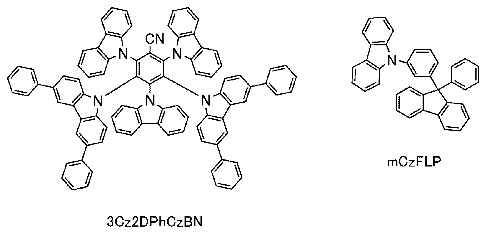

[Tabelle 7]
<<Herstellung einer Licht emittierenden Vorrichtung 10 und von Licht emittierenden Vergleichsvorrichtungen 11 und 12>><< Manufacture of a light-emitting
Die Licht emittierende Vorrichtung 10 und die Licht emittierenden Vergleichsvorrichtungen 11 und 12 wurden durch die gleichen Schritte wie diejenigen für die vorstehend beschriebene Licht emittierende Vorrichtung 1 hergestellt, mit Ausnahme des Schritts zum Ausbilden der Lochtransportschicht
Die Licht emittierende Vorrichtung 10 kann als Licht emittierende Vorrichtung angesehen werden, die durch Hinzufügen eines phosphoreszierenden Materials zu der Licht emittierenden Vergleichsvorrichtung 11 erhalten wird. Die Licht emittierende Vergleichsvorrichtung 11 kann als Licht emittierende Vorrichtung angesehen werden, die durch Hinzufügen eines fluoreszierenden Materials mit Schutzgruppen zu der Licht emittierenden Vergleichsvorrichtung 12 erhalten wird. Daher kann die Licht emittierende Vorrichtung 10 als Licht emittierende Vorrichtung angesehen werden, die durch Hinzufügen eines fluoreszierenden Materials mit Schutzgruppen und eines phosphoreszierenden Materials zu der Licht emittierenden Vergleichsvorrichtung 12 erhalten wird.The light-emitting
Eigenschaften von Licht emittierenden Vorrichtungen>Characteristics of light-emitting devices>
Als Nächstes wurden die Eigenschaften der hergestellten Licht emittierenden Vorrichtung 10 und der hergestellten Licht emittierenden Vergleichsvorrichtungen 11 und 12 gemessen. Es sei angemerkt, dass das Messverfahren demjenigen ähnlich ist, das im Beispiel 1 verwendet wurde.Next, the properties of the manufactured light-emitting
Tabelle 8 zeigt die Vorrichtungseigenschaften der Licht emittierenden Vorrichtung 10 und der Licht emittierenden Vergleichsvorrichtungen 11 und 12 bei etwa 1000 cd/m2.Table 8 shows the device characteristics of the light-emitting
[Tabelle 8]
Wie in
Obwohl die Licht emittierende Vorrichtung 10 Licht emittiere, das aus dem fluoreszierenden Material stammt, weist die Licht emittierende Vorrichtung 10, wie in
Bei der Licht emittierenden Vorrichtung 10 wird ein TADF-Material als Energiedonator verwendet. Bei der Licht emittierenden Vorrichtung einer Ausführungsform der vorliegenden Erfindung kann daher ein TADF-Material vorteilhaft verwendet werden. Bei der Licht emittierenden Vorrichtung 10 wird auch eine organische Verbindung, in der ein Luminophor ein Chinacridon-Gerüst aufweist, als fluoreszierendes Material mit Schutzgruppen verwendet. Bei der Licht emittierenden Vorrichtung einer Ausführungsform der vorliegenden Erfindung kann daher eine organische Verbindung mit einem Chinacridon-Gerüst vorteilhaft verwendet werden.In the
[Beispiel 4][Example 4]
In diesem Beispiel werden Herstellungsbeispiele und Eigenschaften von Licht emittierenden Vorrichtungen und Licht emittierenden Vergleichsvorrichtungen von Ausführungsformen der vorliegenden Erfindung, die sich von denjenigen in dem vorstehenden Beispiel unterscheiden, beschrieben. Die Struktur von jeder der Licht emittierenden Vorrichtungen, die in diesem Beispiel hergestellt wurden, ist die gleiche wie diejenige, die in


[Tabelle 9]
<<Herstellung einer Licht emittierenden Vorrichtung 13>><< Manufacture of a light-emitting
Die Licht emittierende Vorrichtung 13 wurde durch die gleichen Schritte wie diejenigen für die vorstehend beschriebene Licht emittierende Vorrichtung 10 hergestellt, mit Ausnahme des Schritts zum Ausbilden der Licht emittierenden Schicht
<Eigenschaften von Licht emittierenden Vorrichtungen><Characteristics of Light Emitting Devices>
Als Nächstes wurden die Vorrichtungseigenschaften der hergestellten Licht emittierenden Vorrichtung 13 gemessen. Es sei angemerkt, dass das Messverfahren demjenigen ähnlich ist, das im Beispiel 1 verwendet wurde.Next, the device characteristics of the manufactured light-emitting
Tabelle 10 zeigt die Vorrichtungseigenschaften der Licht emittierenden Vorrichtung 13 bei etwa 3 cd/m2.Table 10 shows the device characteristics of the light-emitting
[Tabelle 10]
Wie in
Obwohl die Licht emittierende Vorrichtung 13 Licht emittierte, das aus dem fluoreszierenden Material stammt, wies sie, wie in
(Referenzbeispiel 1)(Reference example 1)
In diesem Referenzbeispiel wird ein Syntheseverfahren von 2TMSmmtBuDPhA2Anth (Strukturformel (229)), das ein fluoreszierendes Material mit Schutzgruppen ist, das in den Beispielen 1 und 2 verwendet wurde, beschrieben.In this reference example, a synthesis method of 2TMSmmtBuDPhA2Anth (structural formula (229)) which is a fluorescent material with protecting groups used in Examples 1 and 2 is described.
<Schritt 1: Synthese von 9,10-Dibrom-2-trimethylsilylanthracen><Step 1: Synthesis of 9,10-dibromo-2-trimethylsilylanthracene>
In einen 500 ml Dreihalskolben wurden zuerst 2,7 g (11 mmol) 2-Trimethylsilylanthracen gegeben, und die Atmosphäre in dem Kolben wurde durch Stickstoff ersetzt. Dazu wurden 110 ml N,N-Dimethylsulfoxid hinzugefügt, und die Mischung wurde bei Raumtemperatur gerührt. Dazu wurden dann 4,0 g (23 mmol) N-Bromsuccinimid hinzugefügt, und die Mischung wurde bei Raumtemperatur 15 Stunden lang gerührt. Nach dem Rühren wurde der Reaktionsmischung Wasser hinzugefügt, um eine wässrige Schicht und eine organische Schicht zu erhalten. Die wässrige Schicht wurde einer Extraktion mit Toluol unterzogen, die extrahierte Lösung und die organische Schicht wurden kombiniert und mit Wasser und einer gesättigten wässrigen Natriumchloridlösung gewaschen, und dann wurde eine Trocknung mit Magnesiumsulfat durchgeführt. Diese Mischung wurde durch Schwerkraftfiltration getrennt, und das Filtrat wurde konzentriert, um einen gelblich braunen Feststoff zu erhalten. Dem resultierenden gelblich braunen Feststoff wurden 450 ml Hexan und 50 ml Toluol hinzugefügt, und dann wurde eine Saugfiltration durch Florisil (Katalog Nr. 066-05265, hergestellt von Wako Pure Chemical Industries, Ltd.), Celite (Katalog Nr. 537-02305, hergestellt von Wako Pure Chemical Industries, Ltd.) und Aluminiumoxid durchgeführt, um ein Filtrat zu erhalten. Das erhaltene Filtrat wurde konzentriert, um einen gelblich braunen Feststoff zu erhalten. Der resultierende Feststoff wurde aus Ethylacetat/Ethanol umkristallisiert, um 2,4 g eines gelben Feststoffs mit einer Ausbeute von 54 % zu erhalten. Ein Syntheseschema (F-1) von Schritt 1 wird nachstehend gezeigt.Into a 500 ml three-necked flask was first placed 2.7 g (11 mmol) of 2-trimethylsilylanthracene, and the atmosphere in the flask was replaced with nitrogen. To this were 110 ml of N, N-dimethyl sulfoxide added and the mixture was stirred at room temperature. Then 4.0 g (23 mmol) of N-bromosuccinimide was added thereto, and the mixture was stirred at room temperature for 15 hours. After stirring, water was added to the reaction mixture to obtain an aqueous layer and an organic layer. The aqueous layer was subjected to extraction with toluene, the extracted solution and the organic layer were combined and washed with water and a saturated sodium chloride aqueous solution, and then drying was carried out with magnesium sulfate. This mixture was separated by gravity filtration and the filtrate was concentrated to give a yellowish brown solid. To the resulting yellowish brown solid were added 450 ml of hexane and 50 ml of toluene, and then suction filtration was carried out through Florisil (Catalog No. 066-05265, manufactured by Wako Pure Chemical Industries, Ltd.), Celite (Catalog No. 537-02305, manufactured by Wako Pure Chemical Industries, Ltd.) and alumina to obtain a filtrate. The obtained filtrate was concentrated to obtain a yellowish brown solid. The resulting solid was recrystallized from ethyl acetate / ethanol to obtain 2.4 g of a yellow solid in a yield of 54%. A synthesis scheme (F-1) of

Die Ergebnisse einer 1H-NMR-Messung des in dem Schritt 1 erhaltenen gelben Feststoffs werden nachstehend beschrieben. Die 1H-NMR-Diagramme werden in
1H-NMR (CDCIs, 300 MHz): σ = 8,74 (s, 1H), 8,63-8,56 (m, 2H), 8,55 (d, J = 8,8 Hz, 1H), 7,75 (d, J = 8,3 Hz, 1H), 7,68-7,61 (m, 2H), 0,42 (s, 9H) 1 H-NMR (CDCIs, 300 MHz): σ = 8.74 (s, 1H), 8.63-8.56 (m, 2H), 8.55 (d, J = 8.8 Hz, 1H) , 7.75 (d, J = 8.3 Hz, 1H), 7.68-7.61 (m, 2H), 0.42 (s, 9H)
<Schritt 2: Synthese von 2TMS-mmtBuDPhA2Anth><Step 2: Synthesis of 2TMS-mmtBuDPhA2Anth>
In einen 200 ml Dreihalskolben wurden 1,4 g (3,3 mmol) 9,10-Dibrom-2-trimethylsilylanthracen, 2,6 g (6,6 mmol) Bis(3,5-tert-butylphenyl)amin, 1,3 g (14 mmol) Natrium-tert-butoxid und 60 mg (0,15 mmol) 2-Dicyclohexylphosphino-2',6'-dimethoxy-1,1'-biphenyl (Abkürzung: SPhos) gegeben, und die Luft in dem Kolben wurde durch Stickstoff ersetzt. Dieser Mischung wurden 33 ml Xylol hinzugefügt, die resultierende Mischung wurde unter reduziertem Druck entgast, der Mischung wurden 40 mg (70 µmo9l) Bis(dibenzylidenaceton)palladium(0) hinzugefügt, und dann wurde die resultierende Mischung bei 150 °C 6 Stunden lang unter einem Stickstoffstrom gerührt. Nach dem Rühren wurden der erhaltenen Mischung 400 ml Toluol hinzugefügt, und es wurde eine Saugfiltration durch Florisil, Celite und Aluminiumoxid durchgeführt, um ein Filtrat zu erhalten. Das erhaltene Filtrat wurde konzentriert, um einen braunen Feststoff zu erhalten. Dieser Feststoff wurde durch Kieselgel-Säulenchromatographie (Hexan: Toluol = 9:1 als Laufmittel) gereinigt, um einen gelben Feststoff zu erhalten. Der erhaltene gelbe Feststoff wurde aus Ethylacetat und Ethanol umkristallisiert, um 0,40 g eines gelben Zielfeststoffs, der eine Zielsubstanz war, mit einer Ausbeute von 12 % zu erhalten. Das Syntheseschema (F-2) von Schritt 2 wird nachstehend gezeigt.1.4 g (3.3 mmol) of 9,10-dibromo-2-trimethylsilylanthracene, 2.6 g (6.6 mmol) of bis (3,5-tert-butylphenyl) amine, 1, 3 g (14 mmol) of sodium tert-butoxide and 60 mg (0.15 mmol) of 2-dicyclohexylphosphino-2 ', 6'-dimethoxy-1,1'-biphenyl (abbreviation: SPhos) are added, and the air in the Flask was replaced with nitrogen. To this mixture, 33 ml of xylene was added, the resulting mixture was degassed under reduced pressure, 40 mg (70 µmo9l) of bis (dibenzylidene acetone) palladium (0) was added to the mixture, and then the resulting mixture was kept at 150 ° C for 6 hours stirred in a stream of nitrogen. After stirring, 400 ml of toluene was added to the resulting mixture, and suction filtration was carried out through Florisil, Celite and alumina to obtain a filtrate. The resulting filtrate was concentrated to obtain a brown solid. This solid was purified by silica gel column chromatography (hexane: toluene = 9: 1 as an eluent) to obtain a yellow solid. The yellow solid obtained was recrystallized from ethyl acetate and ethanol to obtain 0.40 g of a target yellow solid, which was a target substance, in a yield of 12%. The synthesis scheme (F-2) of
![]()
![]()

Durch ein Train-Sublimationsverfahren wurden 0,40 g des erhaltenen gelben Feststoffs durch Sublimation gereinigt. Bei der Sublimationsreinigung wurde der gelbe Feststoff unter einem Druck von 3,5 Pa 15 Stunden lang bei 260 °C erwärmt. Nach der Sublimationsreinigung wurden 0,35 g eines gelben Zielfeststoffs mit einer Sammelquote von 87 % erhalten.By a train sublimation method, 0.40 g of the yellow solid obtained was purified by sublimation. In the sublimation purification, the yellow solid was heated under a pressure of 3.5 Pa for 15 hours at 260 ° C. After sublimation purification, 0.35 g of a target yellow solid was obtained with a collection rate of 87%.
Die Ergebnisse einer 1H-NMR-Messung des in dem Schritt 2 erhaltenen gelben Feststoffs werden nachstehend beschrieben. Die 1H-NMR-Diagramme werden in
1H-NMR (CDCIs, 300 MHz): σ = 8,25 (s, 1H), 8,24-8,21 (m, 1H), 8,15-8,11 (m, 2H), 7,40-7,37 (m, 1H), 7,30-7,27(m, 2H), 6,97-6,94 (m, 8H), 6,92-6,91 (m, 4H), 1,14 (s, 36H), 1,12 (m, 36H), 0,09 (s, 9H) 1 H-NMR (CDCIs, 300 MHz): σ = 8.25 (s, 1H), 8.24-8.21 (m, 1H), 8.15-8.11 (m, 2H), 7, 40-7.37 (m, 1H), 7.30-7.27 (m, 2H), 6.97-6.94 (m, 8H), 6.92-6.91 (m, 4H), 1.14 (s, 36H), 1.12 (m, 36H), 0.09 (s, 9H)
(Referenzbeispiel 2)(Reference example 2)
In diesem Referenzbeispiel wird ein Syntheseverfahren von Oct-tBuDPQd (Strukturformel (104)), das ein fluoreszierendes Material mit Schutzgruppen ist, das in den Beispielen 3 und 4 verwendet wurde, beschrieben.In this reference example, a synthesis method of Oct-tBuDPQd (structural formula (104)) which is a fluorescent material with protecting groups used in Examples 3 and 4 is described.
<Schritt 1: Synthese von 1,4-Cyclohexadien-1,4-dicarbonsäure und 2,5-Bis{(3,5-di-tert-butylphenyl)amino }-dimethylester><Step 1: Synthesis of 1,4-cyclohexadiene-1,4-dicarboxylic acid and 2,5-bis {(3,5-di-tert-butylphenyl) amino} dimethyl ester>
In einen 200 ml Dreihalskolben, der mit einem Rücklaufrohr ausgestattet war, wurden 5,6 g (24 mmol) 1,4-Cyclohexandion-2,5-dicarbonsäuredimethyl und 10 g (48 mmol) 3,5-Di-tert-butylanilin gegeben, und diese Mischung wurde 2 Stunden lang bei 170 °C gerührt. Methanol wurde dem erhaltenen rötlich orangenen Feststoff hinzugefügt, um einen Schlamm zu bilden, und die Mischung wurde durch Saugfiltration gesammelt. Der resultierende Feststoff wurde mit Hexan und Methanol gewaschen und getrocknet, so dass 12 g eines rötlich orangenen Zielfeststoffs mit einer Ausbeute von 82 % erhalten wurden. Ein Syntheseschema (E-1) von Schritt 1 wird nachstehend gezeigt.In a 200 ml three-necked flask equipped with a reflux tube, 5.6 g (24 mmol) 1,4-cyclohexanedione-2,5-dicarboxylic acid dimethyl and 10 g (48 mmol) 3,5-di-tert-butylaniline were placed , and this mixture was stirred at 170 ° C for 2 hours. Methanol was added to the resulting reddish orange solid to form a slurry, and the mixture was collected by suction filtration. The resulting solid was washed with hexane and methanol and dried to give 12 g of a target reddish orange solid in a yield of 82%. A synthesis scheme (E-1) of

Die numerischen 1H-NMR-Daten des resultierenden Feststoffs sind wie folgt. Die Daten offenbaren, dass eine Zielverbindung erhalten wurde.The 1 H-NMR numerical data of the resulting solid is as follows. The data reveals that a target connection was obtained.
1H-NMR (Chloroform-d, 500 MHz): δ = 10,6 (s, 2H), 7,20 (t, J = 1,5 Hz, 2H), 6,94 (d, J = 2,0 Hz, 4H), 3,65 (s, 6H), 3,48 (s, 4H), 1,33 (s, 36H) 1 H-NMR (chloroform-d, 500 MHz): δ = 10.6 (s, 2H), 7.20 (t, J = 1.5 Hz, 2H), 6.94 (d, J = 2, 0 Hz, 4H), 3.65 (s, 6H), 3.48 (s, 4H), 1.33 (s, 36H)
<Schritt 2: Synthese von 1,4-Benzoldicarbonsäure und 2,5-Bis{(3,5-di-tert-butylphenyl)amino }-dimethylester><Step 2: Synthesis of 1,4-benzene dicarboxylic acid and 2,5-bis {(3,5-di-tert-butylphenyl) amino} dimethyl ester>
In einen 300 ml Dreihalskolben, der mit einem Rücklaufrohr ausgestattet war, wurden 12 g (20 mmol) 1,4-Cyclohexadien-1,4-dicarbonsäure, die in dem Schritt 1 erhalten worden waren, 2,5-Bis{(3,5-di-tert-butylphenyl)amino}-dimethylester und 150 ml Toluol gegeben. Die Mischung wurde 15 Stunden lang durch Blasen bzw. Bubbling von Luft refluxiert. Nach dem Rühren wurde der ausgefällte Feststoff durch Saugfiltration gesammelt, und der resultierende Feststoff wurde mit Hexan und Methanol gewaschen, so dass 7,3 g eines roten Zielfeststoffs erhalten wurden. Das erhaltene Filtrat wurde konzentriert, um einen Feststoff ferner zu erhalten. Dieser Feststoff wurde mit Hexan und Methanol gewaschen und durch Saugfiltration gesammelt, so dass 3,1 g eines roten Zielfeststoffs erhalten wurden. Daher wurden insgesamt 10,4 g der Zielverbindungen mit einer Ausbeute von 85 % erhalten. Ein Syntheseschema (E-2) von Schritt 2 wird nachstehend gezeigt.Into a 300 ml three-necked flask equipped with a reflux pipe, 12 g (20 mmol) of 1,4-cyclohexadiene-1,4-dicarboxylic acid obtained in the

Die numerischen 1H-NMR-Daten des resultierenden Feststoffs sind wie folgt. Die Daten offenbaren, dass eine Zielverbindung erhalten wurde.The 1 H-NMR numerical data of the resulting solid is as follows. The data reveals that a target connection was obtained.
1H-NMR (Chloroform-d, 500 MHz): δ = 8,84 (s, 2H), 8,18 (s, 2H), 7,08 (d, J = 2,0 Hz, 4H), 7,20 (t, J = 1,0 Hz, 2H), 3,83 (s, 6H), 1,34 (s, 36H) 1 H-NMR (chloroform-d, 500 MHz): δ = 8.84 (s, 2H), 8.18 (s, 2H), 7.08 (d, J = 2.0 Hz, 4H), 7 .20 (t, J = 1.0 Hz, 2H), 3.83 (s, 6H), 1.34 (s, 36H)
<Schritt 3: Synthese von 1,4-Benzoldicarbonsäure und 2,5-Bis[N,N'-bis(3,5-di-tert-butylphenyl)am ino]-dimethylester><Step 3: Synthesis of 1,4-benzenedicarboxylic acid and 2,5-bis [N, N'-bis (3,5-di-tert-butylphenyl) am ino] dimethyl ester>
In einen 200 ml Dreihalskolben, der mit einem Rücklaufrohr ausgestattet war, wurden 4,0 g (6,7 mmol) 1,4-Benzoldicarbonsäure und 2,5-Bis{(3,5-di-tert-butylphenyl)amino}-dimethylester, die in dem Schritt 2 erhalten worden waren, 3,9 g (14,6 mmol) 1-Brom-3,5-di-tert-butylbenzol, 0,46 g (7,3 mmol) Kupfer, 50 mg (0,26 mmol) Kupferiodid, 1,0 g (7,3 mmol) Kaliumcarbonat und 10 ml Xylol gegeben. Die Mischung wurde bei reduziertem Druck entgast, und die Luft in dem Kolben wurde durch Stickstoff ersetzt. Diese Mischung wurde 20 Stunden lang refluxiert. Der resultierenden Mischung wurden 0,46 g (7,3 mmol) Kupfer und 50 mg Kupferiodid (0,26 mmol) hinzugefügt, und die Mischung wurde weiter 16 Stunden lang refluxiert. Der resultierenden Mischung wurde Dichlormethan hinzugefügt, um einen Schlamm zu bilden. Durch Saugfiltration wurde der Feststoff entfernt, und das erhaltene Filtrat wurde konzentriert. Der erhaltene Feststoff wurde mit Hexan und Ethanol gewaschen. Der gewaschene Feststoff wurde aus Hexan/Toluol umkristallisiert, um 4,4 g eines gelben Feststoffs, der eine Zielverbindung war, mit einer Ausbeute von 72 % zu erhalten. Ein Syntheseschema (E-3) von Schritt 3 wird nachstehend gezeigt.In a 200 ml three-necked flask equipped with a reflux tube, 4.0 g (6.7 mmol) of 1,4-benzenedicarboxylic acid and 2,5-bis {(3,5-di-tert-butylphenyl) amino} - dimethyl esters obtained in

Die numerischen 1H-NMR-Daten des resultierenden Feststoffs sind wie folgt. Die Daten offenbaren, dass eine Zielverbindung erhalten wurde.The 1 H-NMR numerical data of the resulting solid is as follows. The data reveals that a target connection was obtained.
1H-NMR (Chloroform-d, 500 MHz): δ = 7,48 (s, 2H), 6,97 (t, J = 2,0 Hz, 4H), 7,08 (d, J = 1,5 Hz, 8H), 3,25 (s, 6H), 1,23 (s, 72H) 1 H-NMR (chloroform-d, 500 MHz): δ = 7.48 (s, 2H), 6.97 (t, J = 2.0 Hz, 4H), 7.08 (d, J = 1, 5 Hz, 8H), 3.25 (s, 6H), 1.23 (s, 72H)
<Schritt 4: Synthese von 1,3,8,10-Tetra-tert-butyl-7,14-bis(3,5-di-tert-butylphenyl)-5,12-dihydrochino[2,3-b]acridin-7,14-dion (Abkürzung: Oct-tBuDPQd)><Step 4: Synthesis of 1,3,8,10-tetra-tert-butyl-7,14-bis (3,5-di-tert-butylphenyl) -5,12-dihydrochino [2,3-b] acridine -7,14-dione (Abbreviation: Oct-tBuDPQd)>
In einen 100 ml Dreihalskolben, der mit einem Rücklaufrohr ausgestattet war, wurden 4,4 g (4,8 mmol) 1,4-Benzoldicarbonsäure und 2,5-Bis[N,N'-bis(3,5-di-tert-butylphenyl)amino]-dimethylester, die in dem Schritt 3 erhalten worden waren, und 20 ml Methansulfonat gegeben, und die Mischung wurde 7 Stunden lang bei 160 °C gerührt. Die Mischung wurde auf Raumtemperatur abgekühlt, langsam in 300 ml Eiswasser gegossen und dann liegen gelassen, bis sie auf Raumtemperatur kam. Diese Mischung wurde durch Schwerkraftfiltration gefiltert, und der resultierende Feststoff wurde mit Wasser und einer gesättigten wässrigen Natriumhydrogencarbonat-Lösung gewaschen. Dieser Feststoff wurde in Toluol aufgelöst, die erhaltene Toluollösung wurde mit Wasser und einer gesättigten Salzlösung gewaschen, und eine Trocknung wurde mit Magnesiumsulfat durchgeführt. Diese Mischung wurde durch Celite (hergestellt von Wako Pure Chemical Industries, Ltd., Katalog Nr. 537-02305) und Aluminiumoxid gefiltert. Das erhaltene Filtrat wurde konzentriert, um 3,3 g eines schwärzlich braunen Feststoffs zu erhalten. Der resultierende Feststoff wurde durch Kieselgel-Säulenchromatographie (Hexan: Ethylacetat = 20:1 als Laufmittel) gereinigt, um 150 mg eines rötlich orangenen Feststoffs, der eine Zielverbindung war, mit einer Ausbeute von 5 % zu erhalten. Das Syntheseschema (E-4) von Schritt 4 wird nachstehend gezeigt.4.4 g (4.8 mmol) 1,4-benzenedicarboxylic acid and 2,5-bis [N, N'-bis (3,5-di-tert -butylphenyl) amino] dimethyl ester obtained in the
Die Ergebnisse einer 1H-NMR-Messung des in dem Schritt 4 erhaltenen gelben Feststoffs werden nachstehend beschrieben. Die 1H-NMR-Diagramme werden in
1H-NMR (Chloroform-d, 500 MHz): δ = 8,00 (s, 2H), 7,65 (t, J = 2,0 Hz, 2H), 7,39 (d, J = 1,0 Hz, 4H), 7,20 (d, J = 2,0 Hz, 2H), 6,50 (d, J = 1,0 Hz, 2H), 1,60 (s, 18H), 1,39 (s, 36H), 1,13 (s, 18H) 1 H-NMR (chloroform-d, 500 MHz): δ = 8.00 (s, 2H), 7.65 (t, J = 2.0 Hz, 2H), 7.39 (d, J = 1, 0 Hz, 4H), 7.20 (d, J = 2.0 Hz, 2H), 6.50 (d, J = 1.0 Hz, 2H), 1.60 (s, 18H), 1.39 (s, 36H), 1.13 (s, 18H)
BezugszeichenlisteList of reference symbols
- 100100
- EL-Schicht,EL layer,
- 101101
- Elektrode,Electrode,
- 102102
- Elektrode,Electrode,
- 106106
- Licht emittierende Einheit,Light emitting unit,
- 108108
- Licht emittierende Einheit,Light emitting unit,
- 111111
- Lochinjektionsschicht,Hole injection layer,
- 112112
- Lochtransportschicht,Hole transport layer,
- 113113
- Elektronentransportschicht,Electron transport layer,
- 114114
- Elektroneninjektionsschicht,Electron injection layer,
- 115115
- Ladungserzeugungsschicht,Charge generation layer,
- 116116
- Lochinjektionsschicht,Hole injection layer,
- 117117
- Lochtransportschicht,Hole transport layer,
- 118118
- Elektronentransportschicht,Electron transport layer,
- 119119
- Elektroneninjektionsschicht,Electron injection layer,
- 120120
- Licht emittierende Schicht,Light-emitting layer,
- 130130
- Licht emittierende Schicht,Light-emitting layer,
- 131131
- Verbindung,Connection,
- 132132
- Verbindung,Connection,
- 133133
- Verbindung,Connection,
- 135135
- Verbindung,Connection,
- 136136
- Verbindung,Connection,
- 150150
- Licht emittierende Vorrichtung,Light emitting device,
- 170170
- Licht emittierende Schicht,Light-emitting layer,
- 250250
- Licht emittierende Vorrichtung,Light emitting device,
- 301301
- Gastmaterial,Guest material,
- 302302
- Gastmaterial,Guest material,
- 310310
- Luminophor,Luminophore,
- 320320
- Schutzgruppe,Protecting group,
- 330330
- Wirtsmaterial,Host material,
- 601601
- Source-Treiberschaltung,Source driver circuit,
- 602602
- Pixelabschnitt,Pixel section,
- 603603
- Gate-Treiberschaltung,Gate driver circuit,
- 604604
- Dichtungssubstrat,Sealing substrate,
- 605605
- Dichtungsmittel,Sealant,
- 607607
- Raum,Room,
- 608608
- Leitung,Management,
- 609609
- FPC,FPC,
- 610610
- Elementsubstrat,Element substrate,
- 611611
- Schalt-TFT,Switching TFT,
- 612612
- Stromsteuer-TFT,Power control TFT,
- 613613
- Elektrode,Electrode,
- 614614
- Isolator,Insulator,
- 616616
- EL-Schicht,EL layer,
- 617617
- Elektrode,Electrode,
- 618618
- Licht emittierende Vorrichtung,Light emitting device,
- 623623
- n-Kanal-TFT,n-channel TFT,
- 624624
- p-Kanal-TFT,p-channel TFT,
- 625625
- Trocknungsmittel,Desiccant,
- 900900
- tragbares Informationsendgerät,portable information terminal,
- 901901
- Gehäuse,Casing,
- 902902
- Gehäuse,Casing,
- 903903
- Anzeigeabschnitt,Display section,
- 905905
- Gelenkabschnitt,Joint section,
- 910910
- tragbares Informationsendgerät,portable information terminal,
- 911911
- Gehäuse,Casing,
- 912912
- Anzeigeabschnitt,Display section,
- 913913
- Bedienknopf,Control button,
- 914914
- externer Verbindungsanschluss,external connection port,
- 915915
- Lautsprecher,Speaker,
- 916916
- Mikrofon,Microphone,
- 917917
- Kamera,Camera,
- 920920
- Kamera,Camera,
- 921921
- Gehäuse,Casing,
- 922922
- Anzeigeabschnitt,Display section,
- 923923
- Bedienknopf,Control button,
- 924924
- Auslöseknopf,Release button,
- 926926
- Linse,Lens,
- 10011001
- Substrat,Substrate,
- 10021002
- Basis-Isolierfilm,Base insulating film,
- 10031003
- Gate-Isolierfilm,Gate insulating film,
- 10061006
- Gate-Elektrode,Gate electrode,
- 10071007
- Gate-Elektrode,Gate electrode,
- 10081008
- Gate-Elektrode,Gate electrode,
- 10201020
- Zwischenschicht-Isolierfilm,Interlayer insulating film,
- 10211021
- Zwischenschicht-Isolierfilm,Interlayer insulating film,
- 10221022
- Elektrode,Electrode,
- 1024B1024B
- Elektrode,Electrode,
- 1024G1024G
- Elektrode,Electrode,
- 1024R1024R
- Elektrode,Electrode,
- 1024W1024W
- Elektrode,Electrode,
- 1025B1025B
- untere Elektrode,lower electrode,
- 1025G1025G
- untere Elektrode,lower electrode,
- 1025R1025R
- untere Elektrode,lower electrode,
- 1025W1025W
- untere Elektrode,lower electrode,
- 10261026
- Trennwand,Partition wall,
- 10281028
- EL-Schicht,EL layer,
- 10291029
- Elektrode,Electrode,
- 10311031
- Dichtungssubstrat,Sealing substrate,
- 10321032
- Dichtungsmittel,Sealant,
- 10331033
- Basismaterial,Base material,
- 1034B1034B
- Farbschicht,Paint layer,
- 1034G1034G
- Farbschicht,Paint layer,
- 1034R1034R
- Farbschicht,Paint layer,
- 10361036
- Abdeckungsschicht,Cover layer,
- 10371037
- Zwischenschicht-Isolierfilm,Interlayer insulating film,
- 10401040
- Pixelabschnitt,Pixel section,
- 10411041
- Treiberschaltungsabschnitt,Driver circuit section,
- 10421042
- Peripherieabschnitt,Peripheral section,
- 21002100
- Roboter,Robot,
- 21012101
- Beleuchtungsstärkesensor,Illuminance sensor,
- 21022102
- Mikrofon,Microphone,
- 21032103
- obere Kamera,upper camera,
- 21042104
- Lautsprecher,Speaker,
- 21052105
- Display,Display,
- 21062106
- untere Kamera,lower camera,
- 21072107
- Hindernissensor,Obstacle sensor,
- 21082108
- Bewegungsmechanismus,Movement mechanism,
- 21102110
- arithmetische Einheit,arithmetic unit,
- 50005000
- Gehäuse,Casing,
- 50015001
- Anzeigeabschnitt,Display section,
- 50025002
- Anzeigeabschnitt,Display section,
- 50035003
- Lautsprecher,Speaker,
- 50045004
- LED-Lampe,Led lamp,
- 50055005
- Bedientaste,Control button,
- 50065006
- Verbindungsanschluss,Connection port,
- 50075007
- Sensor,Sensor,
- 50085008
- Mikrofon,Microphone,
- 50125012
- Stütze,Support,
- 50135013
- Ohrhörer,Earphones,
- 51005100
- Reinigungsroboter,Cleaning robot,
- 51015101
- Display,Display,
- 51025102
- Kamera,Camera,
- 51035103
- Bürste,Brush,
- 51045104
- Bedienknopf,Control button,
- 51205120
- Staub,Dust,
- 51405140
- tragbares elektronisches Gerät,portable electronic device,
- 51505150
- tragbares Informationsendgerät,portable information terminal,
- 51515151
- Gehäuse,Casing,
- 51525152
- Anzeigebereich,Display area,
- 51535153
- Biegeabschnitt,Bending section,
- 85018501
- Beleuchtungsvorrichtung,Lighting device,
- 85028502
- Beleuchtungsvorrichtung,Lighting device,
- 85038503
- Beleuchtungsvorrichtung,Lighting device,
- 85048504
- BeleuchtungsvorrichtungLighting device
Diese Anmeldung basiert auf der japanischen Patentanmeldung mit der Seriennr.
ZITATE ENTHALTEN IN DER BESCHREIBUNGQUOTES INCLUDED IN THE DESCRIPTION
Diese Liste der vom Anmelder aufgeführten Dokumente wurde automatisiert erzeugt und ist ausschließlich zur besseren Information des Lesers aufgenommen. Die Liste ist nicht Bestandteil der deutschen Patent- bzw. Gebrauchsmusteranmeldung. Das DPMA übernimmt keinerlei Haftung für etwaige Fehler oder Auslassungen.This list of the documents listed by the applicant was generated automatically and is included solely for the better information of the reader. The list is not part of the German patent or utility model application. The DPMA assumes no liability for any errors or omissions.
Zitierte PatentliteraturPatent literature cited
- JP 2018131254 [0417]JP 2018131254 [0417]
Zitierte Nicht-PatentliteraturNon-patent literature cited
- Hiroki Noda et al., Sci. Adv. 2018, 4 [0011]Hiroki Noda et al., Sci. Adv. 2018, 4 [0011]
- S. Wang et al., Angew. Chem., Int. Ed. 2015, 54, 13068 [0011]S. Wang et al., Angew. Chem., Int. Ed. 2015, 54, 13068 [0011]
Claims (24)
Applications Claiming Priority (3)
| Application Number | Priority Date | Filing Date | Title |
|---|---|---|---|
| JP2018131254 | 2018-07-11 | ||
| JP2018-131254 | 2018-07-11 | ||
| PCT/IB2019/055705 WO2020012304A1 (en) | 2018-07-11 | 2019-07-04 | Light-emitting device, display device, electronic device, organic compound, and lighting device |
Publications (1)
| Publication Number | Publication Date |
|---|---|
| DE112019003481T5 true DE112019003481T5 (en) | 2021-04-08 |
Family
ID=69142289
Family Applications (1)
| Application Number | Title | Priority Date | Filing Date |
|---|---|---|---|
| DE112019003481.2T Pending DE112019003481T5 (en) | 2018-07-11 | 2019-07-04 | Light emitting device, display device, electronic device, organic compound and lighting device |
Country Status (6)
| Country | Link |
|---|---|
| JP (3) | JP7440219B2 (en) |
| KR (2) | KR102833740B1 (en) |
| CN (1) | CN112437990A (en) |
| DE (1) | DE112019003481T5 (en) |
| TW (2) | TW202500719A (en) |
| WO (1) | WO2020012304A1 (en) |
Families Citing this family (13)
| Publication number | Priority date | Publication date | Assignee | Title |
|---|---|---|---|---|
| WO2020022378A1 (en) | 2018-07-27 | 2020-01-30 | 出光興産株式会社 | Compound, material for organic electroluminescence element, organic electroluminescence element, and electronic device |
| TW202030902A (en) | 2018-09-12 | 2020-08-16 | 德商麥克專利有限公司 | Electroluminescent devices |
| TWI826522B (en) * | 2018-09-12 | 2023-12-21 | 德商麥克專利有限公司 | Electroluminescent devices |
| KR20210089685A (en) * | 2018-11-09 | 2021-07-16 | 가부시키가이샤 한도오따이 에네루기 켄큐쇼 | A light emitting device, a light emitting device, a display device, an electronic device, and a lighting device |
| JP7341172B2 (en) | 2019-02-06 | 2023-09-08 | 株式会社半導体エネルギー研究所 | Light emitting devices, electronic equipment and lighting equipment |
| JPWO2020217129A1 (en) * | 2019-04-25 | 2020-10-29 | ||
| US20220267668A1 (en) * | 2019-05-10 | 2022-08-25 | Semiconductor Energy Laboratory Co., Ltd. | Light-emitting device, light-emitting appliance, display device, electronic appliance, and lighting device |
| US20230312458A1 (en) * | 2020-07-03 | 2023-10-05 | Semiconductor Energy Laboratory Co., Ltd. | Compound, light-emitting device, light-emitting apparatus, electronic device, and alighting device |
| CN116368957A (en) * | 2020-09-18 | 2023-06-30 | 三星显示有限公司 | Organic Electroluminescent Devices |
| KR102898805B1 (en) | 2020-12-29 | 2025-12-10 | 엘지디스플레이 주식회사 | Organic light emitting diode and organic light emitting device including the same |
| CN112909211B (en) * | 2021-01-25 | 2023-11-14 | 京东方科技集团股份有限公司 | Material for forming blue light-emitting layer, light-emitting device, light-emitting substrate and light-emitting device |
| US20240130225A1 (en) * | 2021-01-28 | 2024-04-18 | Semiconductor Energy Laboratory Co., Ltd. | Light-emitting device, light-emitting apparatus, electronic device, display device, and lighting device |
| CN115041588A (en) | 2021-03-08 | 2022-09-13 | 株式会社Lg新能源 | Foil tab forming device and foil tab forming method |
Family Cites Families (12)
| Publication number | Priority date | Publication date | Assignee | Title |
|---|---|---|---|---|
| JP2002256168A (en) | 2001-03-05 | 2002-09-11 | Toyo Ink Mfg Co Ltd | Fluorescent colorant |
| US6863997B2 (en) | 2001-12-28 | 2005-03-08 | The Trustees Of Princeton University | White light emitting OLEDs from combined monomer and aggregate emission |
| JP4263700B2 (en) | 2005-03-15 | 2009-05-13 | 出光興産株式会社 | Aromatic amine derivative and organic electroluminescence device using the same |
| US20100314644A1 (en) * | 2009-06-12 | 2010-12-16 | Idemitsu Kosan Co., Ltd. | Organic electroluminescent device |
| TWI679790B (en) | 2012-08-03 | 2019-12-11 | 日商半導體能源研究所股份有限公司 | Light-emitting element |
| JP5905916B2 (en) * | 2013-12-26 | 2016-04-20 | 出光興産株式会社 | Organic electroluminescence device and electronic device |
| JP6374329B2 (en) * | 2014-06-26 | 2018-08-15 | 出光興産株式会社 | ORGANIC ELECTROLUMINESCENT ELEMENT, MATERIAL FOR ORGANIC ELECTROLUMINESCENT ELEMENT, AND ELECTRONIC DEVICE |
| US10950803B2 (en) * | 2014-10-13 | 2021-03-16 | Universal Display Corporation | Compounds and uses in devices |
| KR102146445B1 (en) | 2016-03-31 | 2020-08-20 | 코니카 미놀타 가부시키가이샤 | Luminous thin film and organic electroluminescent device |
| US11302882B2 (en) * | 2016-11-25 | 2022-04-12 | Merck Patent Gmbh | Luminescent film, organic electroluminescent element, organic material composition and method for producing organic electroluminescent element |
| JPWO2018186462A1 (en) * | 2017-04-07 | 2020-02-27 | コニカミノルタ株式会社 | Fluorescent compound, organic material composition, luminescent film, organic electroluminescent device material, and organic electroluminescent device |
| US11557743B2 (en) * | 2018-01-17 | 2023-01-17 | Konica Minolta, Inc. | Luminescent film, organic electroluminescent device, and method for manufacturing organic electroluminescent device |
-
2019
- 2019-07-04 KR KR1020207036916A patent/KR102833740B1/en active Active
- 2019-07-04 KR KR1020257022981A patent/KR20250109799A/en active Pending
- 2019-07-04 DE DE112019003481.2T patent/DE112019003481T5/en active Pending
- 2019-07-04 WO PCT/IB2019/055705 patent/WO2020012304A1/en not_active Ceased
- 2019-07-04 CN CN201980046592.1A patent/CN112437990A/en active Pending
- 2019-07-09 TW TW113133598A patent/TW202500719A/en unknown
- 2019-07-09 TW TW108124158A patent/TWI856017B/en active
- 2019-07-10 JP JP2019128184A patent/JP7440219B2/en active Active
-
2024
- 2024-02-15 JP JP2024021204A patent/JP7681743B2/en active Active
-
2025
- 2025-05-12 JP JP2025079998A patent/JP2025114780A/en active Pending
Also Published As
| Publication number | Publication date |
|---|---|
| TW202005955A (en) | 2020-02-01 |
| WO2020012304A1 (en) | 2020-01-16 |
| TW202500719A (en) | 2025-01-01 |
| JP2020017721A (en) | 2020-01-30 |
| US20210280811A1 (en) | 2021-09-09 |
| JP2025114780A (en) | 2025-08-05 |
| JP7681743B2 (en) | 2025-05-22 |
| CN112437990A (en) | 2021-03-02 |
| JP7440219B2 (en) | 2024-02-28 |
| TWI856017B (en) | 2024-09-21 |
| KR102833740B1 (en) | 2025-07-15 |
| KR20250109799A (en) | 2025-07-17 |
| KR20210030278A (en) | 2021-03-17 |
| JP2024040466A (en) | 2024-03-25 |
Similar Documents
| Publication | Publication Date | Title |
|---|---|---|
| DE112018002586B4 (en) | Electronic device, display device, electronic device and lighting device | |
| JP7480372B2 (en) | Light-emitting element, light-emitting device, electronic device and lighting device | |
| DE112019003481T5 (en) | Light emitting device, display device, electronic device, organic compound and lighting device | |
| DE112019002407T5 (en) | Light-emitting element, display device, electronic device, organic compound and lighting device | |
| DE112018005320T5 (en) | Organic compound, light emitting element, light emitting device, electronic device and lighting device | |
| DE112019005603B4 (en) | Light-emitting device, light-emitting apparatus, display device, electronic device and lighting device | |
| DE112017002347T5 (en) | Light-emitting element, display device, electronic device and lighting device | |
| DE102017206649A1 (en) | Light-emitting element, display device, electronic device and lighting device | |
| DE112020001143T5 (en) | Light-emitting device, light-emitting device, display device, electronic device and lighting device | |
| DE112018004962T5 (en) | Light emitting element, display device, electronic device and lighting device | |
| DE102021107060A1 (en) | Arylamine compound, material for hole transport layer, material for hole injection layer, light-emitting device, light-emitting device, electronic device and lighting device | |
| DE112019004580T5 (en) | Light emitting device, light emitting device, electronic device and lighting device | |
| DE112018001365T5 (en) | Organic compound, light-emitting element, light-emitting device, electronic device and lighting device | |
| DE112019008059B4 (en) | Organic compound and binucleate complex | |
| DE112019002747T5 (en) | Organic compound, light-emitting element, light-emitting device, electronic device and lighting device | |
| DE102020122459A1 (en) | Connection, light emitting device, light emitting device, electronic device and lighting device | |
| DE102020118101A1 (en) | Organic compound, light-emitting device, light-receiving device, light-emitting device, light-emitting module, electronic device and lighting device | |
| DE112018000748B4 (en) | Organic compound, light-emitting element, light-emitting device, electronic device, and lighting device | |
| DE112021003575T5 (en) | Light-emitting device, light-emitting device, electronic device, and lighting device | |
| DE102019200635A1 (en) | Organic compound, light-emitting element, light-emitting device, electronic device and lighting device | |
| DE102020134845A1 (en) | Connection, light emitting device, light emitting device, electronic device and lighting device | |
| DE112021003574T5 (en) | Organic compound, light-emitting device, light-emitting device, electronic device, and lighting device | |
| DE102020132680A1 (en) | Organic compound, optical device, light-emitting device, light-emitting device, electronic device and lighting device | |
| DE112019003873B4 (en) | Organic compound, light-emitting element, light-emitting device, electronic device and lighting device | |
| DE102020118101B4 (en) | Organic compound, light-emitting device, light-receiving device, light-emitting device, light-emitting module, electronic device and lighting device |
Legal Events
| Date | Code | Title | Description |
|---|---|---|---|
| R012 | Request for examination validly filed | ||
| R016 | Response to examination communication |