DE112004002027T5 - Acoustically coupled film transformer - Google Patents
Acoustically coupled film transformer Download PDFInfo
- Publication number
- DE112004002027T5 DE112004002027T5 DE112004002027T DE112004002027T DE112004002027T5 DE 112004002027 T5 DE112004002027 T5 DE 112004002027T5 DE 112004002027 T DE112004002027 T DE 112004002027T DE 112004002027 T DE112004002027 T DE 112004002027T DE 112004002027 T5 DE112004002027 T5 DE 112004002027T5
- Authority
- DE
- Germany
- Prior art keywords
- acoustic
- fbar
- fbars
- fact
- electrodes
- Prior art date
- Legal status (The legal status is an assumption and is not a legal conclusion. Google has not performed a legal analysis and makes no representation as to the accuracy of the status listed.)
- Granted
Links
Classifications
-
- H—ELECTRICITY
- H03—ELECTRONIC CIRCUITRY
- H03H—IMPEDANCE NETWORKS, e.g. RESONANT CIRCUITS; RESONATORS
- H03H9/00—Networks comprising electromechanical or electro-acoustic elements; Electromechanical resonators
- H03H9/46—Filters
- H03H9/54—Filters comprising resonators of piezoelectric or electrostrictive material
- H03H9/58—Multiple crystal filters
- H03H9/60—Electric coupling means therefor
- H03H9/605—Electric coupling means therefor consisting of a ladder configuration
-
- H—ELECTRICITY
- H03—ELECTRONIC CIRCUITRY
- H03H—IMPEDANCE NETWORKS, e.g. RESONANT CIRCUITS; RESONATORS
- H03H9/00—Networks comprising electromechanical or electro-acoustic elements; Electromechanical resonators
- H03H9/02—Details
- H03H9/02007—Details of bulk acoustic wave devices
- H03H9/02086—Means for compensation or elimination of undesirable effects
- H03H9/02102—Means for compensation or elimination of undesirable effects of temperature influence
-
- H—ELECTRICITY
- H03—ELECTRONIC CIRCUITRY
- H03H—IMPEDANCE NETWORKS, e.g. RESONANT CIRCUITS; RESONATORS
- H03H9/00—Networks comprising electromechanical or electro-acoustic elements; Electromechanical resonators
- H03H9/02—Details
- H03H9/125—Driving means, e.g. electrodes, coils
- H03H9/13—Driving means, e.g. electrodes, coils for networks consisting of piezoelectric or electrostrictive materials
- H03H9/132—Driving means, e.g. electrodes, coils for networks consisting of piezoelectric or electrostrictive materials characterized by a particular shape
-
- H—ELECTRICITY
- H03—ELECTRONIC CIRCUITRY
- H03H—IMPEDANCE NETWORKS, e.g. RESONANT CIRCUITS; RESONATORS
- H03H9/00—Networks comprising electromechanical or electro-acoustic elements; Electromechanical resonators
- H03H9/15—Constructional features of resonators consisting of piezoelectric or electrostrictive material
- H03H9/17—Constructional features of resonators consisting of piezoelectric or electrostrictive material having a single resonator
- H03H9/171—Constructional features of resonators consisting of piezoelectric or electrostrictive material having a single resonator implemented with thin-film techniques, i.e. of the film bulk acoustic resonator [FBAR] type
- H03H9/172—Means for mounting on a substrate, i.e. means constituting the material interface confining the waves to a volume
- H03H9/175—Acoustic mirrors
-
- H—ELECTRICITY
- H03—ELECTRONIC CIRCUITRY
- H03H—IMPEDANCE NETWORKS, e.g. RESONANT CIRCUITS; RESONATORS
- H03H9/00—Networks comprising electromechanical or electro-acoustic elements; Electromechanical resonators
- H03H9/46—Filters
- H03H9/54—Filters comprising resonators of piezoelectric or electrostrictive material
- H03H9/58—Multiple crystal filters
- H03H9/582—Multiple crystal filters implemented with thin-film techniques
- H03H9/583—Multiple crystal filters implemented with thin-film techniques comprising a plurality of piezoelectric layers acoustically coupled
- H03H9/584—Coupled Resonator Filters [CFR]
-
- H—ELECTRICITY
- H03—ELECTRONIC CIRCUITRY
- H03H—IMPEDANCE NETWORKS, e.g. RESONANT CIRCUITS; RESONATORS
- H03H9/00—Networks comprising electromechanical or electro-acoustic elements; Electromechanical resonators
- H03H9/46—Filters
- H03H9/54—Filters comprising resonators of piezoelectric or electrostrictive material
- H03H9/58—Multiple crystal filters
- H03H9/582—Multiple crystal filters implemented with thin-film techniques
- H03H9/586—Means for mounting to a substrate, i.e. means constituting the material interface confining the waves to a volume
- H03H9/587—Air-gaps
-
- H—ELECTRICITY
- H03—ELECTRONIC CIRCUITRY
- H03H—IMPEDANCE NETWORKS, e.g. RESONANT CIRCUITS; RESONATORS
- H03H9/00—Networks comprising electromechanical or electro-acoustic elements; Electromechanical resonators
- H03H9/46—Filters
- H03H9/54—Filters comprising resonators of piezoelectric or electrostrictive material
- H03H9/58—Multiple crystal filters
- H03H9/582—Multiple crystal filters implemented with thin-film techniques
- H03H9/586—Means for mounting to a substrate, i.e. means constituting the material interface confining the waves to a volume
- H03H9/589—Acoustic mirrors
-
- H—ELECTRICITY
- H03—ELECTRONIC CIRCUITRY
- H03H—IMPEDANCE NETWORKS, e.g. RESONANT CIRCUITS; RESONATORS
- H03H9/00—Networks comprising electromechanical or electro-acoustic elements; Electromechanical resonators
- H03H9/46—Filters
- H03H9/54—Filters comprising resonators of piezoelectric or electrostrictive material
- H03H9/58—Multiple crystal filters
- H03H9/60—Electric coupling means therefor
-
- H—ELECTRICITY
- H03—ELECTRONIC CIRCUITRY
- H03H—IMPEDANCE NETWORKS, e.g. RESONANT CIRCUITS; RESONATORS
- H03H9/00—Networks comprising electromechanical or electro-acoustic elements; Electromechanical resonators
- H03H9/0023—Networks for transforming balanced signals into unbalanced signals and vice versa, e.g. baluns, or networks having balanced input and output
- H03H9/0095—Networks for transforming balanced signals into unbalanced signals and vice versa, e.g. baluns, or networks having balanced input and output using bulk acoustic wave devices
Landscapes
- Physics & Mathematics (AREA)
- Acoustics & Sound (AREA)
- Chemical & Material Sciences (AREA)
- Crystallography & Structural Chemistry (AREA)
- Piezo-Electric Or Mechanical Vibrators, Or Delay Or Filter Circuits (AREA)
Abstract
Ein
akustisch gekoppelter Filmtransformator (FACT = Film Acoustically-Coupled
Transformer), der folgende Merkmale aufweist:
einen entkoppelten,
gestapelten, akustischen Volumenresonator (DSBAR = Decaupled Stacked
Bulk Acoustic Resonator), der folgende Merkmale aufweist:
einen
unteren akustischen Filmvolumenresonator (FBAR = Film Bulk Resonator),
einen oberen FBAR, der auf dem unteren FBAR gestapelt ist, wobei
jeder der FBARs gegenüberliegende
planare Elektroden und ein piezoelektrisches Element zwischen den
Elektroden aufweist, und
einen akustischen Entkoppler, der
eine Schicht eines akustischen Entkopplungsmaterials aufweist, zwischen
den FBARs;
erste Anschlüsse,
die elektrisch mit den Elektroden des unteren FBAR verbunden sind;
und
zweite Anschlüsse,
die elektrisch mit den Elektroden des oberen FBAR verbunden sind.An acoustically coupled film transformer (FACT = Film Acoustically-Coupled Transformer), comprising:
a decoupled, stacked, volume deconvolved acoustic resonator (DSBAR) comprising:
a lower film bulk resonator (FBAR), an upper FBAR stacked on the lower FBAR, each of the FBARs having opposed planar electrodes and a piezoelectric element between the electrodes, and
an acoustic decoupler comprising a layer of acoustic decoupling material between the FBARs;
first terminals electrically connected to the electrodes of the lower FBAR; and
second terminals electrically connected to the upper FBAR electrodes.
Description
Hintergrund der Erfindungbackground the invention
Transformatoren werden bei vielen Typen einer elektronischen Vorrichtung verwendet, um derartige Funktionen durchzuführen, wie ein Transformieren von Impedanzen, ein Verbinden einer einendigen Schaltungsanordnung mit einer symmetrischen Schaltungsanordnung oder umgekehrt und ein Liefern einer elektrischen Isolation. Jedoch weisen nicht alle Transformatoren alle diese Eigenschaften auf. Beispielsweise liefert ein Autotransformator keine elektrische Isolation.transformers are used in many types of electronic device, to perform such functions, like transforming impedances, connecting a single-ended one Circuit arrangement with a symmetrical circuit arrangement or vice versa and providing electrical isolation. however Not all transformers have all these characteristics. For example, an autotransformer does not provide electrical isolation.
Transformatoren, die bei Audio- und Funkfrequenzen bis zu VHF wirksam sind, sind häufig als gekoppelte primäre und sekundäre Wicklungen um einen Kern mit hoher Permeabilität gebaut. Der Kern enthält den magnetischen Fluss und erhöht die Kopplung zwischen den Wicklungen. Ein Transformator, der in diesem Frequenzbereich wirksam ist, kann ferner unter Verwendung eines optischen Kopplers realisiert werden. Ein Optokoppler, der bei diesem Modus verwendet wird, wird auf dem Gebiet als ein Optoisolator bezeichnet.transformers, which are effective at audio and radio frequencies up to VHF often as a coupled primary and secondary Windings built around a core with high permeability. The core contains the magnetic River and raised the coupling between the windings. A transformer in this frequency range is effective, may also be using an optical coupler can be realized. An optocoupler, the used in this mode is considered in the field as an optoisolator designated.
Bei Transformatoren, die auf gekoppelten Windungen oder Optokopplern basieren, wird das elektrische Eingangssignal in eine unterschiedliche Form (d. h. einen magnetischen Fluss oder Photonen) umgewandelt, die mit einer geeigneten Transformationsstruktur (d. h. einer anderen Wicklung oder einem Lichtdetektor) in Wechselwirkung tritt, und wird an dem Ausgang als ein elektrisches Signal wiederhergestellt. Beispielsweise wandelt ein Optokoppler ein elektrisches Eingangssignal unter Verwendung einer Licht emittierenden Diode in Photonen um. Die Photonen durchlaufen eine optische Faser oder einen freien Raum, der eine Isolation liefert. Eine Photodiode, die durch die Photonen beleuchtet wird, erzeugt ein elektrisches Ausgangssignal aus dem Photonenstrom. Das elektrische Ausgangssignal ist eine Nachbildung des elektrischen Eingangssignals.at Transformers operating on coupled windings or optocouplers are based, the electrical input signal in a different Shape (i.e., a magnetic flux or photons), those with a suitable transformation structure (i.e. Winding or a light detector), and is restored at the output as an electrical signal. For example, an optocoupler converts an electrical input signal using a light emitting diode in photons. The photons pass through an optical fiber or a free space, which provides an isolation. A photodiode, through the photons is illuminated, generates an electrical output signal from the photon current. The electrical output signal is a replica of the electrical Input signal.
Bei UHF und Mikrowellenfrequenzen werden spulenbasierte Transformatoren unpraktisch auf Grund derartiger Faktoren wie Verlusten in dem Kern, Verlusten in den Wicklungen, einer Kapazität zwischen den Wicklungen und einer Schwierigkeit, dieselben klein genug zu machen, um wellenlängenbezogene Probleme zu verhindern. Transformatoren für derartige Frequenzen basieren auf Viertelwellenlängen-Übertragungsleitungen, z. B. Marchand-Typ-, verbundene Reiheneingangs-/Parallelausgangsleitungen, etc. Es existieren auch Transformatoren, die auf mikrobearbeiteten gekoppelten Spulensätzen basieren und klein genug sind, dass Wellenlängenwirkungen unwichtig sind. Derartige Transformatoren weisen jedoch Probleme mit einem hohen Einfügungsverlust auf.at UHF and microwave frequencies become coil-based transformers impractical due to such factors as losses in the core, Losses in the windings, a capacity between the windings and a difficulty in making them small enough to be wavelength-related Prevent problems. Transformers based on such frequencies on quarter-wavelength transmission lines, z. B. Marchand type, connected row input / parallel output lines, etc. There are also transformers based on micromachined coupled coil sets and are small enough that wavelength effects are unimportant. However, such transformers have problems with a high insertion loss on.
Alle eben beschriebenen Transformatoren für eine Verwendung bei UHF und Mikrowellenfrequenzen weisen Abmessungen auf, die dieselben für eine Verwendung bei modernen Miniaturanwendungen mit hoher Dichte wie Mobiltelefonen weniger erwünscht machen. Derartige Transformatoren neigen ferner dazu, kostspielig zu sein, weil dieselben nicht in der Lage sind, durch einen Stapelprozess hergestellt zu werden, und weil dieselben im Wesentlichen eine chipexterne Lösung sind. Obwohl derartige Transformatoren typischerweise eine Bandbreite aufweisen, die für eine Verwendung bei Mobiltelefonen annehmbar ist, weisen dieselben zudem typischerweise einen Einfügungsverlust von mehr als 1 dB auf, was zu hoch ist.All just described transformers for use in UHF and Microwave frequencies have dimensions that are the same for use in modern high-density miniature applications such as mobile phones less desirable do. Such transformers also tend to be expensive because they are not able to be through a batch process and because they are essentially off-chip solution are. Although such transformers typically have a bandwidth have, for a use with mobile phones is acceptable, have the same also typically an insertion loss of more than 1 dB, which is too high.
Optokoppler werden auf Grund der Übergangskapazität der Eingangs-LED, Nichtlinearitäten, die dem Photodetektor inhärent sind, und einer ungenügenden Isolation, um eine gute Gleichtaktunterdrückung zu ergeben, nicht bei UHF und Mikrowellenfrequenzen verwendet.optocoupler are due to the transient capacitance of the input LED, Nonlinearities inherent in the photodetector are, and an insufficient Isolation, to give a good common-mode rejection, not at UHF and microwave frequencies used.
Was deshalb benötigt wird, ist ein Transformator, der bei elektrischen Frequenzen in dem Bereich von UHF bis Mikrowelle zum Liefern eines oder mehrerer der folgenden Attribute in der Lage ist: Impedanztransformation, Kopplung zwischen symmetrischen und unsymmetrischen Schaltungen und elektrische Isolation. Was ferner benötigt wird, ist ein derartiger Transformator, der einen geringen Einfügungsverlust, eine Bandbreite, die ausreichend ist, um beispielsweise den Frequenzbereich von Mobiltelefon-HF-Signalen aufzunehmen, eine kleinere Größe als Transformatoren, die gegenwärtig in Mobiltelefonen verwendet werden, und geringe Herstellungskosten aufweist.What therefore needed is a transformer that is at electrical frequencies in the range from UHF to microwave to deliver one or more the following attributes: impedance transformation, Coupling between balanced and unbalanced circuits and electrical insulation. What is further needed is one such Transformer that has a low insertion loss, a bandwidth, which is sufficient, for example, the frequency range of mobile phone RF signals a smaller size than transformers, the present used in mobile phones, and low manufacturing costs having.
Zusammenfassung der ErfindungSummary the invention
Bei einem ersten Aspekt sieht die Erfindung einen akustisch gekoppelten Filmtransformator (FACT = Film Acoustically-Coupled Transformer) vor, der einen entkoppelten, gestapelten, akustischen Volumenresonator (DSBAR = Decoupled Stacked Bulk Acoustic Resonator) aufweist, der einen unteren akustischen Filmvolumenresonator (FBAR = Film Bulk Resonator), einen oberen FBAR, der auf dem unteren FBAR gestapelt ist, und zwischen den FBARs einen akustischen Entkoppler aufweist, der eine Schicht eines akustischen Entkopplungsmaterials aufweist. Jeder der FBARs weist gegenüberliegende planare Elektroden und ein piezoelektrisches Element zwischen den Elektroden auf. Der FACT weist zusätzlich erste Anschlüsse, die elektrisch mit den Elektroden von einem der FBARs verbunden sind, und zweite Anschlüsse auf, die elektrisch mit den Elektroden des anderen der FBARs verbunden sind. Ein FACT gemäß diesem Aspekt der Erfindung weist ein Impedanztransformationsverhältnis von 1:1 auf, ist zum Verbinden einer einendigen Schaltungsanordnung mit einer symmetrischen Schaltungsanordnung oder umgekehrt in der Lage und liefert eine elektrische Isolation zwischen Primärseite und Sekundärseite.In a first aspect, the invention provides a film acoustically-coupled transformer (FACT) comprising a decoupled stacked bulk acoustic acoustic resonator (DSBAR) including a lower acoustic film volume resonator (FBAR = Film Bulk Resonator), an upper FBAR, which is stacked on the lower FBAR and having an acoustic decoupler between the FBARs comprising a layer of acoustic decoupling material. Each of the FBARs has opposing planar electrodes and a piezoelectric element between the electrodes. The FACT additionally has first terminals electrically connected to the electrodes of one of the FBARs and second terminals electrically connected to the electrodes of the other of the FBARs. A FACT according to this aspect of the invention has an impedance transformation ratio of 1: 1, is capable of connecting a single-ended circuit arrangement to a balanced circuit arrangement, or vice versa, and provides electrical isolation between the primary side and the secondary side.
Bei einem anderen Aspekt sieht die Erfindung einen akustisch gekoppelten Filmtransformator (FACT) vor, der entkoppelte, gestapelte, akustische Volumenresonatoren (DSBARs) aufweist. Jeder der DSBARs weist einen unteren akustischen Filmvolumenresonator (FBAR), einen oberen FBAR, der auf dem unteren FBAR gestapelt ist, und zwischen den FBARs einen akustischen Entkoppler auf, der eine Schicht eines akustischen Entkopplungsmaterials aufweist. Jeder FBAR weist gegenüberliegende planare Elektroden und ein piezoelektrisches Element zwischen den Elektroden auf. Der FACT weist zusätzlich eine erste elektrische Schaltung, die die unteren FBARs verbindet, und eine zweite elektrische Schaltung auf, die die oberen FBARs verbindet. Alle Ausführungsbeispiele eines FACT gemäß diesem Aspekt der Erfindung sind zum Verbinden einer einendigen Schaltungsanordnung mit einer symmetrischen Schaltungsanordnung oder umgekehrt in der Lage und Liefern eine elektrische Isolation zwischen Primärseite und Sekundärseite.at In another aspect, the invention provides an acoustically coupled one Film transformer (FACT), which decoupled, stacked, acoustic Volume resonators (DSBARs) has. Each of the DSBARs has one lower acoustic film volume resonator (FBAR), an upper FBAR, which is stacked on the lower FBAR, and one between the FBARs acoustic decoupler comprising a layer of acoustic decoupling material having. Each FBAR has opposite planar electrodes and a piezoelectric element between the Electrodes on. The FACT additionally has a first electrical Circuit that connects the lower FBARs, and a second electrical Circuit that connects the upper FBARs. All embodiments a FACT according to this Aspect of the invention are for connecting a single-ended circuit arrangement with a symmetrical circuit arrangement or vice versa in the Location and supply an electrical isolation between the primary side and Secondary side.
Einige Ausführungsbeispiele des FACT gemäß diesem Aspekt der Erfindung sind inhärent elektrisch symmetrisch und weisen ein höheres Gleichtaktunterdrückungsverhältnis als das oben beschriebene Ausführungsbeispiel auf, das den einzigen DSBAR aufweist. Bei derartigen Ausführungsbeispielen schaltet die erste elektrische Schaltung einen der FBARs des ersten DSBAR entweder antiparallel oder in Reihe mit einem der FBARs des zweiten DSBAR und die zweite elektrische Schaltung schaltet den anderen der FBARs des ersten DSBAR entweder antiparallel oder in Reihe mit dem anderen der FBARs des zweiten DSBAR. Ein Ausführungsbeispiel des FACT, bei dem die erste elektrische Schaltung die jeweiligen FBARs antiparallel schaltet und die zweite elektrische Schaltung die jeweiligen FBARs antiparallel schaltet, weist ein Impedanztransformationsverhältnis von 1:1 zwischen der ersten elektrischen Schaltung und der zweiten elektrischen Schaltung und umgekehrt auf. Ein Ausführungsbeispiel, bei dem die erste elektrische Schaltung die jeweiligen FBARs in Reihe schaltet und die zweite elektrische Schaltung die jeweiligen FBARs in Reihe schaltet, weist ebenfalls ein Impedanztransformationsverhältnis von 1:1 zwischen der ersten elektrischen Schaltung und der zweiten elektrischen Schaltung und umgekehrt auf. Jedoch sind die Impedanzen höher als bei dem Ausführungsbeispiel, bei dem die FBARs antiparallel geschaltet sind. Ein Ausführungsbeispiel des FACT, bei dem die erste elektrische Schaltung die jeweiligen FBARs antiparallel schaltet und die zweite elektrische Schaltung die jeweiligen FBARs in Reihe schaltet, weist ein Impedanztransformationsverhältnis von 1:4 zwischen der ersten elektrischen Schaltung und der zweiten elektrischen Schaltung und ein Impedanztransformationsverhältnis von 4:1 zwischen der zweiten elektrischen Schaltung und der ersten elektrischen Schaltung auf. Ein Ausführungsbeispiel des FACT, bei dem die erste elektrische Schaltung die jeweiligen FBARs in Reihe schaltet und die zweite elektrische Schaltung die jeweiligen FBARs antiparallel schaltet, weist ein Impedanztransformationsverhältnis von 4:1 zwischen der ersten elektrischen Schaltung und der zweiten elektrischen Schaltung und ein Impedanztransformationsverhältnis von 1:4 zwischen der zweiten elektrischen Schaltung und der ersten elektrischen Schaltung auf.Some embodiments of the FACT according to this Aspect of the invention are inherent electrically symmetrical and have a higher common mode rejection ratio than the embodiment described above which has the only DSBAR. In such embodiments The first electrical circuit switches one of the FBARs of the first DSBAR either antiparallel or in series with one of the FBARs of the second DSBAR and the second electrical circuit switches the other of the FBARs of the first DSBAR either antiparallel or in Series with the other of the FBARs of the second DSBAR. An embodiment of the FACT, in which the first electrical circuit, the respective FBARs turn antiparallel and the second electrical circuit the respective FBARs switches in antiparallel, has an impedance transformation ratio of 1: 1 between the first electrical circuit and the second electrical circuit and vice versa. An embodiment, in which the first electrical circuit the respective FBARs in Row switches and the second electrical circuit the respective FBARs in series also has an impedance transformation ratio of 1: 1 between the first electrical circuit and the second electrical Circuit and vice versa. However, the impedances are higher than in the embodiment, at the FBARs are connected in anti-parallel. An embodiment of the FACT, in which the first electrical circuit, the respective FBARs turn antiparallel and the second electrical circuit the respective FBARs in series, has an impedance transformation ratio of 1: 4 between the first electrical circuit and the second electrical Circuit and an impedance transformation ratio of 4: 1 between the second electrical circuit and the first electrical circuit on. An embodiment of the FACT, in which the first electrical circuit, the respective FBARs in series switches and the second electrical circuit the has an impedance transformation ratio of 4: 1 between the first electrical circuit and the second electrical Circuit and an impedance transformation ratio of 1: 4 between the second electrical circuit and the first electrical circuit on.
Andere Ausführungsbeispiele des FACT gemäß der Erfindung sind elektrisch unsymmetrisch und können bei Anwendungen verwendet werden, bei denen ein hohes Gleichtaktunterdrückungsverhältnis weniger wichtig ist. Bei derartigen Ausführungsbeispielen schaltet die erste elektrische Schaltung einen der FBARs des ersten DSBAR elektrisch entweder parallel oder in Antireihe mit einem der FBARs des zweiten DSBAR und schaltet die zweite elektrische Schaltung den anderen der FBARs des ersten DSBAR elektrisch entweder parallel oder in Antireihe mit dem anderen der FBARs des zweiten DSBAR.Other embodiments of the FACT according to the invention are electrically unbalanced and can be used in applications where a high common mode rejection ratio is less important. In such embodiments The first electrical circuit switches one of the FBARs of the first DSBAR electrically either parallel or in anti-row with one of the FBARs of the second DSBAR and turns on the second electrical circuit the other of the FBARs of the first DSBAR electrically either in parallel or in anti-row with the other of the FBARs of the second DSBAR.
Bei einem anderen Aspekt sieht die Erfindung einen akustisch gekoppelten Filmtransformator (FACT) vor, der einen entkoppelten, gestapelten, akustischen Volumenresonator (DSBAR) aufweist. Der DSBAR weist einen unteren akustischen Filmvolumenresonator (FBAR), einen oberen FBAR, der auf dem unteren FBAR gestapelt ist, und einen akustischen Entkoppler auf, der eine Schicht eines akustischen Entkopplungsmaterials aufweist, das eine akustische Impedanz von etwa 2 Mrayl aufweist. Jeder der FBARs weist gegenüberliegende planare Elektroden und ein piezoelektrisches Element zwischen den Elektroden auf. Der FACT weist zusätzlich erste Anschlüsse, die elektrisch mit den Elektroden des unteren FBAR verbunden sind, und zweite Anschlüsse auf, die elektrisch mit den Elektroden des oberen FBAR verbunden sind.at In another aspect, the invention provides an acoustically coupled one Film transformer (FACT) having a decoupled, stacked, acoustic volume resonator (DSBAR). The DSBAR has a lower acoustic film volume resonator (FBAR), an upper FBAR, which is stacked on the lower FBAR, and an acoustic decoupler having a layer of acoustic decoupling material, which has an acoustic impedance of about 2 Mrayl. Everyone who FBARs have opposite planar ones Electrodes and a piezoelectric element between the electrodes on. The FACT has additional first connections, which are electrically connected to the electrodes of the lower FBAR, and second connections on, which are electrically connected to the electrodes of the upper FBAR are.
Kurze Beschreibung der ZeichnungenShort description the drawings
Detaillierte Beschreibungdetailed description
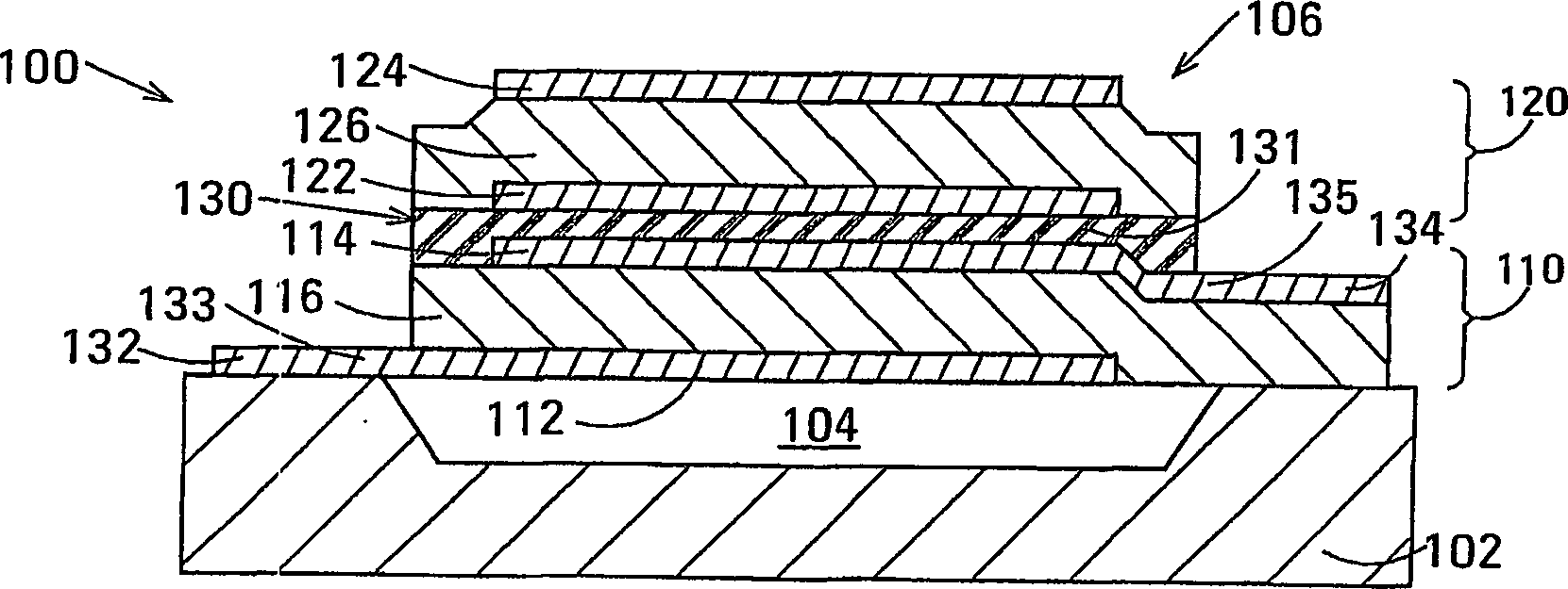
Der
FACT
Bei
dem gezeigten Beispiel sind die ersten Anschlüsse
Bei
dem gezeigten Beispiel ist der DSBAR
FBARs sind durch Ruby et al. in dem US-Patent Nr. 5,587,620 mit dem Titel Tunable Thin Film Acoustic Resonators and Method of Making Same offenbart, das nun an die Anmelderin dieser Offenbarung übertragen ist. Die Offenbarung von Ruby offenbart ferner einen gestapelten, akustischen Filmvolumenresonator (SBAR = Stacked Film Bulk Acoustic Resonator), der aus zwei Schichten eines piezoelektrischen Materials gebildet ist, die mit drei planaren Elektroden verschachtelt sind. Rubys SBAR kann als aus einem gestapelten Paar von FBARs, bei dem eine Elektrode beiden FBARs gemeinsam ist, gebildet betrachtet werden und wird hierin als ein SBAR mit gemeinsamer Elektrode bezeichnet. Die gemeinsame Elektrode macht den SBAR mit gemeinsamer Elektrode unfähig zu einem Verbinden von symmetrischen mit unsymmetrischen Schaltungen und umgekehrt und zu einem Liefern einer elektrischen Isolation zwischen Primärseite und Sekundärseite. Zudem zeigt der SBAR mit gemeinsamer Elektrode eine extrem schmale Durchlassbandbreite, die denselben für eine Verwendung bei den meisten Anwendungen ungeeignet macht. Die schmale Durchlassbandbreite ist das Ergebnis der gemeinsamen Elektrode, die eine akustische Energie zwischen den FBARs überkoppelt.FBARs are by Ruby et al. in U.S. Patent No. 5,587,620, entitled Tunable Thin Film Acoustic Resonators and Method of Making Same which is now assigned to the assignee of this disclosure is. The Ruby disclosure further discloses a stacked, acoustic film volume resonator (SBAR = Stacked Film Bulk Acoustic Resonator), which consists of two layers of piezoelectric material which are nested with three planar electrodes. Ruby SBAR can be considered as a stacked pair of FBARs, where one Electrode is common to both FBARs, formed and is referred to herein as a common electrode SBAR. The common electrode makes the SBAR with common electrode unable to connect balanced and unbalanced circuits and vice versa and to provide electrical isolation between primary and secondary side. In addition, the SBAR with common electrode shows an extremely narrow Passband bandwidth, the same for use in most Makes applications unsuitable. The narrow passband width is the result of the common electrode giving an acoustic energy Coupled between the FBARs.
Wie
es oben angemerkt ist, weist der FACT
Das
Ausführungsbeispiel
des akustischen Entkopplers
Das
akustische Entkopplungsmaterial des akustischen Entkopplers
Das
Ausführungsbeispiel
des akustischen Entkopplers
Allgemeiner
gesagt ist das erste Ausführungsbeispiel
des akustischen Entkopplers
Viele
Kunststoffmaterialien weisen akustische Impedanzen in dem oben angegebenen
Bereich auf und können
in Schichten einheitlicher Dicke in den oben angegebenen Dickenbereichen
aufgebracht sein. Derartige Kunststoffmaterialien sind deshalb potentiell
für eine
Verwendung als das akustische Entkopplungsmaterial der Schicht
Kunststoffmaterialien
weisen typischerweise eine sehr hohe akustische Dämpfung pro
Einheitslänge verglichen
mit den anderen Materialien der FBARs
Bei
einem Ausführungsbeispiel
wird ein Polyimid als das akustische Entkopplungsmaterial der Schicht
Bei
einem anderen Ausführungsbeispiel
wird ein Poly(Para-Xylylen)
als das akustische Entkopplungsmaterial der Schicht
Bei
einem anderen Ausführungsbeispiel
wird ein vernetztes Polyphenylen-Polymer als das akustische Entkopplungsmaterial
der Schicht
Vorläuferlösungen, die verschiedene Oligomere enthalten, die polymerisieren, um jeweilige vernetzte Polyphenylenpolymere zu bilden, werden durch The Dow Chemical Company, Midland, MI unter der Marke SiLK verkauft. Die Vorläuferlösungen werden durch eine Schleuderbeschichtung aufgebracht. Das vernetzte Polyphenylenpolymer, das aus einer dieser Vorläuferlösungen erhalten wird, die als SiLKTM J bezeichnet ist, und das zusätzlich einen Haftverstärker enthält, weist eine berechnete akustische Impedanz von 2,1 Mrayl auf, d. h. etwa 2 Mrayl.Precursor solutions containing various oligomers that polymerize to form respective crosslinked polyphenylene polymers are sold by The Dow Chemical Company, Midland, MI under the trademark SiLK. The precursor solutions are applied by spin coating. The crosslinked polyphenylene polymer obtained from one of these precursor solutions, designated SiLK ™ J, and additionally containing an adhesion promoter, has a calculated acoustic impedance of 2.1 Mrayl, ie, about 2 Mrayl.
Die
Oligomere, die polymerisieren, um vernetzte Polyphenylenpolymere
zu bilden, werden aus Biscyclopentadienon- und aromatischen Acetylen
enthaltenden Monomeren vorbereitet. Ein Verwenden derartiger Monomere
bildet lösliche
Oligomere ohne den Bedarf nach einer unangebrachten Substitution.
Die Vorläuferlösung enthält ein spezifisches
Oligomer, das in Gamma-Butyrolacton- und Cyclohexanon-Lösungsmitteln
gelöst
ist. Der Prozentsatz des Oligomers in der Vorläuferlösung bestimmt die Schichtdicke,
wenn die Vorläuferlösung aufgeschleudert
ist. Nach einer Aufbringung verdampft ein Anlegen von Wärme die
Lösungsmittel
und härtet
dann das Oligomer aus, um ein vernetztes Polymer zu bilden. Die
Biscyclopentadienone reagieren mit den Acetylenen in einer 4 + 2-Cycloadditionsreaktion,
die einen neuen aromatischen Ring bildet. Ein weiteres Aushärten resultiert
in dem vernetzten Polyphenylenpolymer. Die oben beschriebenen vernetzten
Po lyphenylenpolymere sind durch Godschalx et al. in dem US-Patent Nr. 5,965,679
offenbart. Zusätzliche
praktische Details sind durch Martin et al., Development of Low-Dielectric Constant
Polymer for the Fabrication of Integrated Circuit Interconnect,
12 ADVANCED MATERIALS, 1769 (2000) beschrieben. Verglichen mit Polyimid,
weisen vernetzte Polyphenylenpolymere eine niedrigere akustische
Impedanz, eine niedrigere akustische Dämpfung und eine niedrige Dielektrizitätskonstante
auf. Zudem ist eine aufgeschleuderte Schicht der Vorläuferlösung zum
Erzeugen eines qualitativ hochwertigen Films des vernetzten Polyphenylenpolymers
mit einer Dicke in der Größenordnung
von 200 nm in der Lage, was eine typische Dicke des akustischen
Entkopplers
Bei
einem alternativen Ausführungsbeispiel
weist das akustische Entkopplungsmaterial der Schicht
Jede
der Schichten, die die Bragg-Elemente
Bei
einem Ausführungsbeispiel
ist das Bragg-Element
Bei
einem Beispiel weisen die Bragg-Elemente
Bei
Ausführungsbeispielen,
bei denen die akustische Impedanzdifferenz zwischen den Bragg-Elementen
Eine
Wafer-Scale-Fertigung wird verwendet, um FACTs ähnlich dem FACT
Unter
erneuter Bezugnahme auf
In
Betrieb des FACT
Ein
Ausführungsbeispiel
des FACT
Wie
es oben angemerkt ist, liefert der FACT
Der
FACT
Der
DSBAR
Wie
es oben angemerkt ist, verbindet eine elektrische Schaltung einen
der FBARs des DSBAR
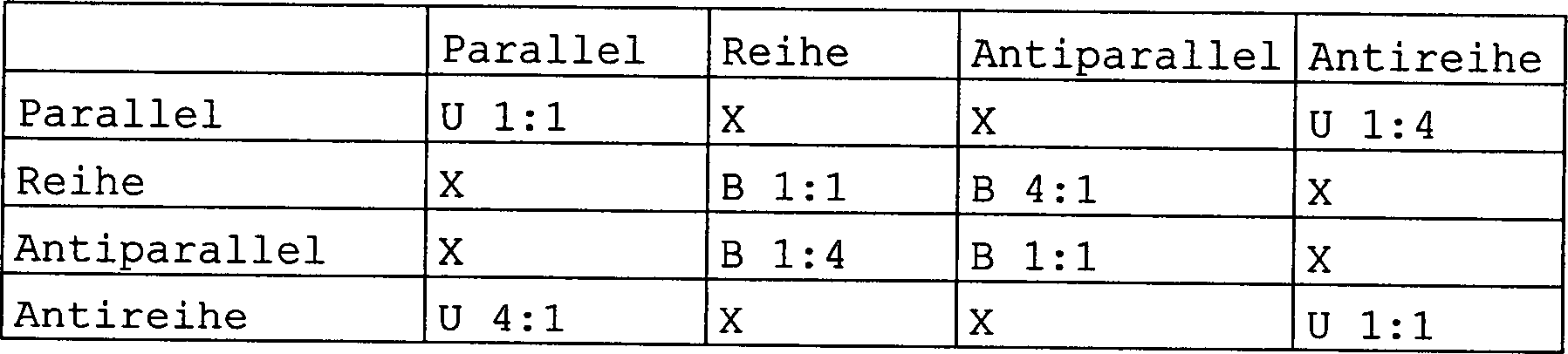
In
Tabelle 1 geben die Zeilenüberschriften
die Konfigurationen von einer der elektrischen Schaltungen an, z.
B. der elektrischen Schaltung
Die
in Tabelle 1 gezeigten elektrischen Schaltungen unterliegen der
Einschränkung,
dass eine elektrische Schaltung lediglich die Elektroden von FBARs
auf der gleichen Ebene wie ein anderer in den DSBARs
Bevor die elektrischen Schaltungen, die die FBARs verbinden, detailliert beschrieben werden, werden die Ausdrücke antiparallel, parallel, Antireihe und Reihe definiert, die auf die elektrischen Schaltungen angewendet werden, die die Elektroden von FBARs unterschiedlicher DSBARs verbinden. Ein FBAR ist eine polaritätsabhängige Vorrichtung. Eine Spannung einer gegebenen Polarität, die zwischen die Elektroden des FBAR angelegt ist, bewirkt, dass sich der FBAR mechanisch zusammenzieht, während die gleiche Spannung der entgegengesetzten Polarität bewirkt, dass sich der FBAR mechanisch um die gleiche Größe ausdehnt. Gleichermaßen erzeugt eine mechanische Belastung, die an den FBAR angelegt ist und die bewirkt, dass sich der FBAR mechanisch zusammenzieht, eine Spannung der gegebenen Polarität zwischen den Elektroden des FBAR, während eine mechanische Belastung, die bewirkt, dass sich der FBAR mechanisch ausdehnt, eine Spannung der entgegengesetzten Polarität zwischen den Elektroden des FBAR erzeugt.Before the electrical circuits connecting the FBARs are detailed be described, the terms antiparallel, parallel, Antireihe and series defined on the electrical circuits be applied, the electrodes of FBARs different DSBARs connect. An FBAR is a polarity dependent device. A tension a given polarity, which is applied between the electrodes of the FBAR, causes the FBAR contracts mechanically, while the same voltage of the opposite polarity causes the FBAR to expand mechanically by the same amount. Equally created a mechanical load applied to the FBAR and the causes the FBAR to contract mechanically, a voltage the given polarity between the electrodes of the FBAR, while a mechanical load, which causes the FBAR to expand mechanically, a voltage of opposite polarity generated between the electrodes of the FBAR.
Mit
Bezug auf
Die Elektroden der FBARs, die eine elektrische Schaltung in Reihe schaltet, befinden sich auf der gleichen Ebene in den jeweiligen DSBARs. Ein Signal, das an die FBARs angelegt ist, die in Reihe geschaltet sind, erzeugt Signale entgegengesetzter Phasen über die FBARs. Die FBARs dehnen sich in Antiphase aus und ziehen sich in Antiphase zusammen, und erzeugen eine akustische Energie in Antiphase. Die Elektroden der FBARs, die eine elektrische Schaltung in Antireihe schaltet, befinden sich jedoch auf unterschiedlichen Ebenen in den jeweiligen DSBARs. Ein Signal, das an die FBARs angelegt ist, die in Antireihe geschaltet sind, erzeugt Signale der gleichen Phase über die FBARs. Die FBARs dehnen sich in Phase aus und ziehen sich in Phase zusammen, und erzeugen eine akustische Energie in Phase.The electrodes of the FBARs, which connect an electrical circuit in series, are at the same level in the respective DSBARs. A signal applied to the FBARs connected in series generates signals of opposite phases over the FBARs. The FBARs expand in antiphase and contract in antiphase, producing an acoustic energy in antiphase. However, the electrodes of the FBARs that switch an anti-series electrical circuit are at different levels in the respective DSBARs. A signal applied to the FBARs connected in anti-series generates signals of the same phase through the FBARs. The FBARs expand in phase and contract in phase, producing an acoustic energy in phase.
FBARs, die eine akustische Energie empfangen, die bewirkt, dass sich dieselben in Phase ausdehnen und in Phase zusammenziehen, erzeugen Signale in Phase. Ein Parallelschalten von FBARs, die Signale in Phase erzeugen, erzeugt einen Signalpegel gleich diesem über die einzelnen FBARs und eine Impedanz von der Hälfte der charakteristischen Impedanz der einzelnen FBARs. Ein Schalten derartiger FBARs in Antireihe erzeugt einen Signalpegel von zwei Mal diesem über die einzelnen FBARs und eine Impedanz von zwei Mal der charakteristischen Impedanz der einzelnen FBARs. Ein Antiparallel- oder in Reihe Schalten von FBARs, die Signale in Phase erzeugen, bewirkt jedoch, dass sich die Signale aufheben. FBARs, die eine akustische Energie empfangen, die bewirkt, dass sich dieselben in Antiphase ausdehnen und in Antiphase zusammenziehen, erzeugen Signale in Antiphase. Ein Antiparallelschalten von FBARs, die Signale in Antiphase erzeugen, erzeugt ein Signal mit einem gleichem Pegel wie diesem über die einzelnen FBARs und eine Impedanz von der Hälfte der charakteristischen Impedanz der einzelnen FBARs. Ein in Reihe Schalten derartiger FBARs erzeugt ein Signal von zwei Mal dem Pegel von diesem über die einzelnen FBARs und eine Impedanz von zwei Mal der charakteristischen Impedanz der einzelnen FBARs. Ein Parallel- oder in Antireihe Schalten von FBARs, die Signale in Antiphase erzeugen, bewirkt jedoch, dass sich die Signale aufheben. Die FACTs, die in Tabelle 1 als nicht funktionsfähig angegeben sind, sind FACTs, bei denen die FBARs, die eine akustische Energie empfangen, Signale erzeugen, die sich aufheben.FBARs who receive an acoustic energy that causes them to be the same expand in phase and contract in phase, generate signals in phase. Parallel connection of FBARs that generate signals in phase, generates a signal level equal to this across the individual FBARs and an impedance of half the characteristic impedance of the individual FBARs. Turn on such anti-series FBARs produce a signal level of two Give this over the individual FBARs and an impedance of twice the characteristic one Impedance of the individual FBARs. An antiparallel or in series switching of FBARs, the Generate signals in phase, however, causes the signals cancel. FBARs that receive an acoustic energy that causes that they expand in antiphase and contract in antiphase, generate signals in antiphase. Anti-parallel switching of FBARs, generate the signals in antiphase, generates a signal with a same level as this over the individual FBARs and an impedance of half the characteristic Impedance of the individual FBARs. A series switching of such FBARs generated a signal of twice the level of this over the individual FBARs and an impedance of twice the characteristic impedance of the individual FBARs. A parallel or antireihe switching of FBARs, the signals in antiphase, but causes the signals to cancel. The FACTs listed as non-functional in Table 1 are FACTs, where the FBARs that receive acoustic energy receive signals generate that cancel each other out.
Genau
gesagt verbindet die elektrische Schaltung
Die
elektrische Schaltung
Es
existiert im Wesentlichen die gleiche Kapazität zwischen jedem der ersten
Anschlüsse
F und dem Substrat
Das
in
Genau
gesagt verbindet die elektrische Schaltung
Die
elektrische Schaltung
Es
existiert im Wesentlichen die gleiche Kapazität zwischen jedem der ersten
Anschlüsse
F und dem Substrat
Das
in
Genau
gesagt verbindet die elektrische Schaltung
Die
elektrische Schaltung
Es
existiert im Wesentlichen die gleiche Kapazität zwischen jedem der ersten
Anschlüssen
F und dem Substrat
Das
in
Das
in
Genau
gesagt verbindet die elektrische Schaltung
Die
elektrische Schaltung
Es
existiert im Wesentlichen die gleiche Kapazität zwischen jedem der ersten
Anschlüsse
F und dem Substrat
Das
in
Das
in
Bei
Anwendungen, bei denen ein niedriges Gleichtaktunterdrückungsverhältnis unwichtig
ist, können elektrische
Schaltungen, die die FBARs verbinden, zu den eben beschriebenen
unterschiedlich sein.
Die
elektrische Konfiguration des Ausführungsbeispiels des FACT
Eine
elektrische Leiterbahn
Bei
einem alternativen Ausführungsbeispiel
sind die Bondanschlussflächen
Eine
Bondanschlussfläche
Bei
dem FACT
Bei
dem in
Der
DSBAR
Tausende
FACTs ähnlich
dem FACT
Es
wird ein Wafer aus Einkristallsilizium bereitgestellt. Ein Abschnitt
des Wafers bildet für
jeden FACT, der gefertigt wird, ein Substrat, das dem Substrat
Der
Abschnitt des Wafers, der das Substrat
Eine
Schicht eines Füllmaterials
(nicht gezeigt) wird an der Oberfläche des Wafers mit einer Dicke
aufgebracht, die ausreichend ist, um die Hohlräume zu füllen. Die Oberfläche des
Wafers wird dann planarisiert, um den Hohlraum mit dem Füllmaterial
gefüllt
zu lassen.
Bei einem Ausführungsbeispiel war das Füllmaterial Phosphosilikatglas (PSG = Phosphosilicate Glass) und wurde unter Verwendung einer herkömmlichen chemischen Niederdruckdampfabscheidung (LPCVD = Low-Pressure Chemical Vapor Deposition) aufgebracht. Das Füllmaterial kann alternativ durch ein Sputtern oder durch eine Schleuderbeschichtung aufgebracht werden.at an embodiment was the filler Phosphosilicate glass (PSG = Phosphosilicate Glass) and was under Using a conventional low-pressure chemical vapor deposition (LPCVD = low-pressure chemical Vapor deposition) applied. The filling material may alternatively applied by sputtering or spin coating become.
Eine
Metallschicht wird an der Oberfläche
des Wafers und dem Füllmaterial
aufgebracht. Das Metall wird strukturiert, um die Elektrode
Die
Metallschichten, in denen die Elektroden
Bei
einem Ausführungsbeispiel
war Molybdän
das Metall, das aufgebracht wurde, um die Elektrode
Eine
Schicht eines piezoelektrischen Materials wird aufgebracht und wird
strukturiert, um eine piezoelektrische Schicht
Bei
einem Ausführungsbeispiel
war Aluminiumnitrid das piezoelektrische Material, das aufgebracht wurde,
um die piezoelektrische Schicht
Eine
Metallschicht wird aufgebracht und wird strukturiert, um die Elektrode
Bei
einem Ausführungsbeispiel
war Molybdän
das Metall, das aufgebracht wurde, um die Elektrode
Eine
Schicht eines akustischen Entkopplungsmaterials wird dann aufgebracht
und strukturiert, um eine akustische Entkopplungsschicht
Bei
einem Ausführungsbeispiel
war das akustische Entkopplungsmaterial Polyimid mit einer Dicke
von etwa 200 nm, d. h. einem Viertel der Mittenfrequenzwellenlänge in dem
Polyimid. Das Polyimid wurde aufgebracht, um die akustische Entkopplungsschicht
Bei
einem Ausführungsbeispiel,
bei dem das Material der akustischen Entkopplungsschicht
Es
wird eine Metallschicht aufgebracht und strukturiert, um die Elektrode
Bei
einem Ausführungsbeispiel
war Molybdän
das Metall, das aufgebracht wurde, um die Elektroden
Eine
Schicht eines piezoelektrischen Materials wird aufgebracht und wird
strukturiert, um die piezoelektrische Schicht
Bei
einem Ausführungsbeispiel
war Aluminiumnitrid das piezoelektrische Material, das aufgebracht wurde,
um die pie zoelektrische Schicht
Eine
Metallschicht wird aufgebracht und wird strukturiert, um die Elektrode
Bei
einem Ausführungsbeispiel
war Molybdän
das Metall, das aufgebracht wurde, um die Elektroden
Der
Wafer wird dann isotropisch nassgeätzt, um das Füllmaterial
Bei
einem Ausführungsbeispiel
war das Ätzmittel,
das verwendet wurde, um das Füllmaterial
Eine
Goldschutzschicht wird an den freiliegenden Oberflächen der
Anschlussflächen
Der
Wafer wird dann in einzelne FACTs geteilt, einschließlich des
FACT
Ein
zu dem Beschriebenen ähnlicher
Prozess kann verwendet werden, um Ausführungsbeispiele des FACT
In
Gebrauch liefern die Bondanschlussfläche
Ein
Ausführungsbeispiel
des FACT
Nachdem
eine Schicht
After a shift
Bei
einem Ausführungsbeispiel
ist Molybdän
das Metall, das aufgebracht wird, um das Bragg-Element mit hoher
akustischer Impedanz zu bilden, das die Elektroden
Eine
Schicht eines Materials mit niedriger akustischer Impedanz wird
dann aufgebracht und wird strukturiert, um ein Bragg-Element mit
niedriger akustischer Impedanz auf eine Weise zu definieren, die
dieser ähnlich
ist, die in
Bei einem Ausführungsbeispiel ist das Material mit niedriger akustischer Impedanz SiO2 mit einer Dicke von etwa 790 nm. Das SiO2 wird durch ein Sputtern aufgebracht und wird durch ein Ätzen strukturiert. Ein anderes Material mit niedriger akustischer Impedanz, das als das Material des Bragg-Elements mit niedriger akustischer Impedanz verwendet werden kann, umfasst Phosphosilikatglas (PSG), Titandioxid und Magnesiumfluorid. Das Material mit niedriger akustischer Impedanz kann alternativ durch andere Verfahren als ein Sputtern aufgebracht werden.at an embodiment is the material with low acoustic impedance SiO2 with a Thickness of about 790 nm. The SiO 2 is deposited by sputtering and is by an etching structured. Another material with low acoustic impedance, as the material of the Bragg element with lower acoustic Impedance can be used includes phosphosilicate glass (PSG), Titanium dioxide and magnesium fluoride. The material with low acoustic Impedance may alternatively be by other than sputtering be applied.
Es
wird eine Metallschicht aufgebracht und strukturiert, um ein Bragg-Element
mit hoher akustischer Impedanz zu definieren, das die Elektroden
Bei
einem Ausführungsbeispiel
ist Molybdän
das Metall, das aufgebracht wird, um ein Bragg-Element mit hoher
akustischer Impedanz zu bilden, das die Elektroden
Eine
Schicht eines piezoelektrischen Materials wird dann aufgebracht
und wird strukturiert, um die piezoelektrische Schicht
Bei
einem anderen Ausführungsbeispiel
ist das akustische Entkopplungsmaterial der Schicht
Eine
Metallschicht wird dann auf der Schicht eines vernetzen Polyphenylenpolymers
auf eine Weise aufgebracht, die ähnlich
dieser ist, die oben mit Bezug auf
Die
Schicht eines vernetzten Polyphenylenpolymers wird dann strukturiert,
wie es in
Die
Metallschicht wird dann wieder strukturiert, wie es in
Eine
Fertigung des Ausführungsbeispiels
des Bandpassfilters
Bei einem Ausführungsbeispiel war die Vorläuferlösung für das vernetzte Polyphenylenpolymer eine, die durch The Dow Chemical Company verkauft wird und als SiLKTM J bezeichnet wird. Alternativ kann die Vorläuferlösung irgendeine Geeignete der Vorläuferlösungen sein, die durch The Dow Chemical Company unter der Marke SiLK verkauft werden. Bei bestimmten Ausführungsbeispielen wurde eine Schicht eines Haftverstärkers aufgebracht, bevor die Vorläuferlösung aufgeschleudert wurde. Vorläuferlösungen, die Oligomere enthalten, die, wenn dieselben ausgehärtet werden, ein vernetztes Polyphenylenpolymer bilden, das eine akustische Impedanz von etwa 2 Mrayl aufweist, können von anderen Lieferanten nun oder zukünftig erhältlich sein und können ebenfalls verwendet werden.In one embodiment, the crosslinked polyphenylene polymer precursor solution was one sold by The Dow Chemical Company and designated SiLK ™ J. Alternatively, the precursor solution may be any suitable one of the precursor solutions sold by The Dow Chemical Company under the trademark SiLK. In certain embodiments, a layer of adhesion promoter was applied before the precursor solution was spin-coated. Precursor solutions containing oligomers which, when cured, form a crosslinked polyphenylene polymer having an acoustic impedance of about 2 Mrayl may be available from other suppliers now or in the future and may also be used.
Diese Offenbarung beschreibt die Erfindung unter Verwendung darstellender Ausführungsbeispiele detailliert. Jedoch ist die Erfindung, die durch die beigefügten Ansprüche definiert ist, nicht auf die beschriebenen, präzisen Ausführungsbeispiele begrenzt.These Disclosure describes the invention using illustrative Detailed embodiments. However, the invention defined by the appended claims is not the described, precise embodiments limited.
ZusammenfassungSummary
Ein
Ausführungsbeispiel
(
Claims (17)
Applications Claiming Priority (5)
| Application Number | Priority Date | Filing Date | Title |
|---|---|---|---|
| US10/699,481 | 2003-10-30 | ||
| US10/699,289 US7019605B2 (en) | 2003-10-30 | 2003-10-30 | Stacked bulk acoustic resonator band-pass filter with controllable pass bandwidth |
| US10/699,289 | 2003-10-30 | ||
| US10/699,481 US6946928B2 (en) | 2003-10-30 | 2003-10-30 | Thin-film acoustically-coupled transformer |
| PCT/US2004/035907 WO2005046053A1 (en) | 2003-10-30 | 2004-10-29 | Film acoustically-coupled transformer |
Publications (2)
| Publication Number | Publication Date |
|---|---|
| DE112004002027T5 true DE112004002027T5 (en) | 2006-08-24 |
| DE112004002027B4 DE112004002027B4 (en) | 2011-09-15 |
Family
ID=34556637
Family Applications (4)
| Application Number | Title | Priority Date | Filing Date |
|---|---|---|---|
| DE112004001968T Expired - Fee Related DE112004001968B4 (en) | 2003-10-30 | 2004-10-29 | Decoupled stacked bulk acoustic resonant band pass filter with controllable passband bandwidth |
| DE112004002027T Expired - Fee Related DE112004002027B4 (en) | 2003-10-30 | 2004-10-29 | Acoustically coupled film transformer |
| DE112004002041.7T Expired - Fee Related DE112004002041B4 (en) | 2003-10-30 | 2004-10-29 | Cavity acoustic volume resonator (FBAR) devices |
| DE112004001996T Expired - Fee Related DE112004001996B4 (en) | 2003-10-30 | 2004-10-29 | Passband bandwidth control in decoupled stacked bulk acoustic resonator devices |
Family Applications Before (1)
| Application Number | Title | Priority Date | Filing Date |
|---|---|---|---|
| DE112004001968T Expired - Fee Related DE112004001968B4 (en) | 2003-10-30 | 2004-10-29 | Decoupled stacked bulk acoustic resonant band pass filter with controllable passband bandwidth |
Family Applications After (2)
| Application Number | Title | Priority Date | Filing Date |
|---|---|---|---|
| DE112004002041.7T Expired - Fee Related DE112004002041B4 (en) | 2003-10-30 | 2004-10-29 | Cavity acoustic volume resonator (FBAR) devices |
| DE112004001996T Expired - Fee Related DE112004001996B4 (en) | 2003-10-30 | 2004-10-29 | Passband bandwidth control in decoupled stacked bulk acoustic resonator devices |
Country Status (5)
| Country | Link |
|---|---|
| US (4) | US7391285B2 (en) |
| JP (4) | JP5101883B2 (en) |
| DE (4) | DE112004001968B4 (en) |
| GB (3) | GB2421647A (en) |
| WO (3) | WO2005043753A1 (en) |
Cited By (1)
| Publication number | Priority date | Publication date | Assignee | Title |
|---|---|---|---|---|
| DE102007002200B4 (en) * | 2006-01-23 | 2017-05-11 | Avago Technologies General Ip (Singapore) Pte. Ltd. | Acoustic Data Coupling System and Method |
Families Citing this family (172)
| Publication number | Priority date | Publication date | Assignee | Title |
|---|---|---|---|---|
| US7275292B2 (en) | 2003-03-07 | 2007-10-02 | Avago Technologies Wireless Ip (Singapore) Pte. Ltd. | Method for fabricating an acoustical resonator on a substrate |
| EP1528677B1 (en) * | 2003-10-30 | 2006-05-10 | Agilent Technologies, Inc. | Film acoustically-coupled transformer with two reverse c-axis piezoelectric elements |
| US7242270B2 (en) * | 2003-10-30 | 2007-07-10 | Avago Technologies Wireless Ip (Singapore) Pte. Ltd. | Decoupled stacked bulk acoustic resonator-based band-pass filter |
| US6946928B2 (en) * | 2003-10-30 | 2005-09-20 | Agilent Technologies, Inc. | Thin-film acoustically-coupled transformer |
| US7332985B2 (en) * | 2003-10-30 | 2008-02-19 | Avago Technologies Wireless Ip (Singapore) Pte Ltd. | Cavity-less film bulk acoustic resonator (FBAR) devices |
| US7391285B2 (en) | 2003-10-30 | 2008-06-24 | Avago Technologies Wireless Ip Pte Ltd | Film acoustically-coupled transformer |
| US7019605B2 (en) * | 2003-10-30 | 2006-03-28 | Larson Iii John D | Stacked bulk acoustic resonator band-pass filter with controllable pass bandwidth |
| US7038559B2 (en) * | 2004-02-23 | 2006-05-02 | Ruby Richard C | Vertically separated acoustic filters and resonators |
| KR100622955B1 (en) * | 2004-04-06 | 2006-09-18 | 삼성전자주식회사 | Thin film bulk acoustic resonator and its manufacturing method |
| US7615833B2 (en) | 2004-07-13 | 2009-11-10 | Avago Technologies Wireless Ip (Singapore) Pte. Ltd. | Film bulk acoustic resonator package and method of fabricating same |
| US7388454B2 (en) | 2004-10-01 | 2008-06-17 | Avago Technologies Wireless Ip Pte Ltd | Acoustic resonator performance enhancement using alternating frame structure |
| US8981876B2 (en) | 2004-11-15 | 2015-03-17 | Avago Technologies General Ip (Singapore) Pte. Ltd. | Piezoelectric resonator structures and electrical filters having frame elements |
| US7202560B2 (en) | 2004-12-15 | 2007-04-10 | Avago Technologies Wireless Ip (Singapore) Pte. Ltd. | Wafer bonding of micro-electro mechanical systems to active circuitry |
| US7791434B2 (en) | 2004-12-22 | 2010-09-07 | Avago Technologies Wireless Ip (Singapore) Pte. Ltd. | Acoustic resonator performance enhancement using selective metal etch and having a trench in the piezoelectric |
| DE102004062312B3 (en) * | 2004-12-23 | 2006-06-01 | Infineon Technologies Ag | Piezoelectric resonator, e.g. in mobile telephones, has a piezoelectric layer with a first resonance frequency temperature coefficient with a first polarity sign and electrodes |
| JP2006203304A (en) * | 2005-01-18 | 2006-08-03 | Hitachi Media Electoronics Co Ltd | Piezoelectric thin film resonator, oscillator using the same, and semiconductor integrated circuit incorporating the same |
| US7427819B2 (en) * | 2005-03-04 | 2008-09-23 | Avago Wireless Ip Pte Ltd | Film-bulk acoustic wave resonator with motion plate and method |
| US7369013B2 (en) * | 2005-04-06 | 2008-05-06 | Avago Technologies Wireless Ip Pte Ltd | Acoustic resonator performance enhancement using filled recessed region |
| US7436269B2 (en) * | 2005-04-18 | 2008-10-14 | Avago Technologies Wireless Ip (Singapore) Pte. Ltd. | Acoustically coupled resonators and method of making the same |
| US7934884B2 (en) * | 2005-04-27 | 2011-05-03 | Lockhart Industries, Inc. | Ring binder cover |
| US7562429B2 (en) * | 2005-06-20 | 2009-07-21 | Avago Technologies General Ip (Singapore) Pte. Ltd. | Suspended device and method of making |
| US7443269B2 (en) | 2005-07-27 | 2008-10-28 | Avago Technologies General Ip (Singapore) Pte. Ltd. | Method and apparatus for selectively blocking radio frequency (RF) signals in a radio frequency (RF) switching circuit |
| US7378781B2 (en) | 2005-09-07 | 2008-05-27 | Nokia Corporation | Acoustic wave resonator with integrated temperature control for oscillator purposes |
| US7868522B2 (en) * | 2005-09-09 | 2011-01-11 | Avago Technologies Wireless Ip (Singapore) Pte. Ltd. | Adjusted frequency temperature coefficient resonator |
| US7391286B2 (en) * | 2005-10-06 | 2008-06-24 | Avago Wireless Ip Pte Ltd | Impedance matching and parasitic capacitor resonance of FBAR resonators and coupled filters |
| US7425787B2 (en) * | 2005-10-18 | 2008-09-16 | Avago Technologies Wireless Ip (Singapore) Pte. Ltd. | Acoustic galvanic isolator incorporating single insulated decoupled stacked bulk acoustic resonator with acoustically-resonant electrical insulator |
| US7423503B2 (en) * | 2005-10-18 | 2008-09-09 | Avago Technologies Wireless Ip (Singapore) Pte. Ltd. | Acoustic galvanic isolator incorporating film acoustically-coupled transformer |
| US7675390B2 (en) | 2005-10-18 | 2010-03-09 | Avago Technologies Wireless Ip (Singapore) Pte. Ltd. | Acoustic galvanic isolator incorporating single decoupled stacked bulk acoustic resonator |
| US7525398B2 (en) * | 2005-10-18 | 2009-04-28 | Avago Technologies General Ip (Singapore) Pte. Ltd. | Acoustically communicating data signals across an electrical isolation barrier |
| US7737807B2 (en) * | 2005-10-18 | 2010-06-15 | Avago Technologies Wireless Ip (Singapore) Pte. Ltd. | Acoustic galvanic isolator incorporating series-connected decoupled stacked bulk acoustic resonators |
| US20070085632A1 (en) * | 2005-10-18 | 2007-04-19 | Larson John D Iii | Acoustic galvanic isolator |
| US7463499B2 (en) * | 2005-10-31 | 2008-12-09 | Avago Technologies General Ip (Singapore) Pte Ltd. | AC-DC power converter |
| US7561009B2 (en) * | 2005-11-30 | 2009-07-14 | Avago Technologies General Ip (Singapore) Pte. Ltd. | Film bulk acoustic resonator (FBAR) devices with temperature compensation |
| US7586392B2 (en) * | 2006-01-23 | 2009-09-08 | Avago Technologies General Ip (Singapore) Pte. Ltd. | Dual path acoustic data coupling system and method |
| US7612636B2 (en) | 2006-01-30 | 2009-11-03 | Avago Technologies Wireless Ip (Singapore) Pte. Ltd. | Impedance transforming bulk acoustic wave baluns |
| US7746677B2 (en) | 2006-03-09 | 2010-06-29 | Avago Technologies Wireless Ip (Singapore) Pte. Ltd. | AC-DC converter circuit and power supply |
| US20070210748A1 (en) * | 2006-03-09 | 2007-09-13 | Mark Unkrich | Power supply and electronic device having integrated power supply |
| US7479685B2 (en) | 2006-03-10 | 2009-01-20 | Avago Technologies General Ip (Singapore) Pte. Ltd. | Electronic device on substrate with cavity and mitigated parasitic leakage path |
| US20070228876A1 (en) * | 2006-03-31 | 2007-10-04 | Chien-Min Sung | Diamond Frequency Control Devices and Associated Methods |
| US7629865B2 (en) | 2006-05-31 | 2009-12-08 | Avago Technologies Wireless Ip (Singapore) Pte. Ltd. | Piezoelectric resonator structures and electrical filters |
| US7598827B2 (en) * | 2006-06-19 | 2009-10-06 | Maxim Integrated Products | Harmonic termination of power amplifiers using BAW filter output matching circuits |
| US7586389B2 (en) * | 2006-06-19 | 2009-09-08 | Maxim Integrated Products, Inc. | Impedance transformation and filter using bulk acoustic wave technology |
| FR2905207B1 (en) * | 2006-08-28 | 2009-01-30 | St Microelectronics Sa | SWITCHABLE FILTER WITH RESONATORS. |
| US7508286B2 (en) * | 2006-09-28 | 2009-03-24 | Avago Technologies Wireless Ip (Singapore) Pte. Ltd. | HBAR oscillator and method of manufacture |
| JP5216210B2 (en) * | 2006-12-28 | 2013-06-19 | 日本電波工業株式会社 | Quartz vibrating piece and quartz vibrating device |
| US7999363B2 (en) * | 2007-01-25 | 2011-08-16 | Alpha & Omega Semiconductor, Ltd | Structure and method for self protection of power device |
| JP2008245243A (en) * | 2007-02-26 | 2008-10-09 | Epson Toyocom Corp | Contour vibrator, adjustment method of contour vibrator |
| US20080202239A1 (en) * | 2007-02-28 | 2008-08-28 | Fazzio R Shane | Piezoelectric acceleration sensor |
| US7786825B2 (en) * | 2007-05-31 | 2010-08-31 | Avago Technologies Wireless Ip (Singapore) Pte. Ltd. | Bulk acoustic wave device with coupled resonators |
| JP5067034B2 (en) * | 2007-06-20 | 2012-11-07 | セイコーエプソン株式会社 | Tuning fork type oscillator, oscillator |
| JP5067035B2 (en) * | 2007-06-20 | 2012-11-07 | セイコーエプソン株式会社 | Tuning fork type oscillator, oscillator |
| US20090079514A1 (en) | 2007-09-24 | 2009-03-26 | Tiberiu Jamneala | Hybrid acoustic resonator-based filters |
| US7791435B2 (en) | 2007-09-28 | 2010-09-07 | Avago Technologies Wireless Ip (Singapore) Pte. Ltd. | Single stack coupled resonators having differential output |
| JP5054491B2 (en) * | 2007-11-21 | 2012-10-24 | パナソニック株式会社 | Piezoelectric vibrator and manufacturing method thereof |
| US8089195B2 (en) * | 2007-12-17 | 2012-01-03 | Resonance Semiconductor Corporation | Integrated acoustic bandgap devices for energy confinement and methods of fabricating same |
| US7732977B2 (en) | 2008-04-30 | 2010-06-08 | Avago Technologies Wireless Ip (Singapore) | Transceiver circuit for film bulk acoustic resonator (FBAR) transducers |
| US7855618B2 (en) | 2008-04-30 | 2010-12-21 | Avago Technologies Wireless Ip (Singapore) Pte. Ltd. | Bulk acoustic resonator electrical impedance transformers |
| JP5226409B2 (en) | 2008-07-17 | 2013-07-03 | 太陽誘電株式会社 | RESONANT DEVICE, COMMUNICATION MODULE, COMMUNICATION DEVICE, AND RESONANT DEVICE MANUFACTURING METHOD |
| US8689426B2 (en) | 2008-12-17 | 2014-04-08 | Sand 9, Inc. | Method of manufacturing a resonating structure |
| KR101289982B1 (en) | 2009-01-09 | 2013-07-26 | 다이요 유덴 가부시키가이샤 | Filter element, branching filter, and electronic apparatus |
| US9735338B2 (en) | 2009-01-26 | 2017-08-15 | Cymatics Laboratories Corp. | Protected resonator |
| US8030823B2 (en) * | 2009-01-26 | 2011-10-04 | Resonance Semiconductor Corporation | Protected resonator |
| US8291559B2 (en) * | 2009-02-24 | 2012-10-23 | Epcos Ag | Process for adapting resonance frequency of a BAW resonator |
| US8902023B2 (en) | 2009-06-24 | 2014-12-02 | Avago Technologies General Ip (Singapore) Pte. Ltd. | Acoustic resonator structure having an electrode with a cantilevered portion |
| US8248185B2 (en) | 2009-06-24 | 2012-08-21 | Avago Technologies Wireless Ip (Singapore) Pte. Ltd. | Acoustic resonator structure comprising a bridge |
| ES2365772B2 (en) * | 2009-07-08 | 2013-05-23 | Universitat Politècnica De Catalunya | DEVICE AND FILTER OF ACOUSTIC WAVE. |
| WO2011036979A1 (en) * | 2009-09-28 | 2011-03-31 | 太陽誘電株式会社 | Acoustic wave device |
| JP5478180B2 (en) * | 2009-09-30 | 2014-04-23 | 太陽誘電株式会社 | filter |
| FR2951024B1 (en) * | 2009-10-01 | 2012-03-23 | St Microelectronics Sa | METHOD FOR MANUFACTURING BAW RESONATOR WITH HIGH QUALITY FACTOR |
| FR2951023B1 (en) * | 2009-10-01 | 2012-03-09 | St Microelectronics Sa | METHOD FOR MANUFACTURING MONOLITHIC OSCILLATORS WITH BAW RESONATORS |
| FR2951026B1 (en) * | 2009-10-01 | 2011-12-02 | St Microelectronics Sa | METHOD FOR MANUFACTURING BAW RESONATORS ON A SEMICONDUCTOR WAFER |
| US8193877B2 (en) | 2009-11-30 | 2012-06-05 | Avago Technologies Wireless Ip (Singapore) Pte. Ltd. | Duplexer with negative phase shifting circuit |
| US9243316B2 (en) | 2010-01-22 | 2016-01-26 | Avago Technologies General Ip (Singapore) Pte. Ltd. | Method of fabricating piezoelectric material with selected c-axis orientation |
| US8796904B2 (en) | 2011-10-31 | 2014-08-05 | Avago Technologies General Ip (Singapore) Pte. Ltd. | Bulk acoustic resonator comprising piezoelectric layer and inverse piezoelectric layer |
| WO2011099381A1 (en) * | 2010-02-09 | 2011-08-18 | 株式会社村田製作所 | Piezoelectric device, and piezoelectric device manufacturing method |
| US8587391B2 (en) * | 2010-02-23 | 2013-11-19 | Avago Technologies General Ip (Singapore) Pte. Ltd. | Acoustic coupling layer for coupled resonator filters and method of fabricating acoustic coupling layer |
| US8283999B2 (en) * | 2010-02-23 | 2012-10-09 | Avago Technologies Wireless Ip (Singapore) Pte. Ltd. | Bulk acoustic resonator structures comprising a single material acoustic coupling layer comprising inhomogeneous acoustic property |
| US8661899B2 (en) | 2010-03-01 | 2014-03-04 | Sand9, Inc. | Microelectromechanical gyroscopes and related apparatus and methods |
| WO2011133682A1 (en) | 2010-04-20 | 2011-10-27 | Guiti Zolfagharkhani | Microelectromechanical gyroscopes and related apparatus and methods |
| US9479139B2 (en) | 2010-04-29 | 2016-10-25 | Avago Technologies General Ip (Singapore) Pte. Ltd. | Resonator device including electrode with buried temperature compensating layer |
| US9197185B2 (en) * | 2010-04-29 | 2015-11-24 | Avago Technologies General Ip (Singapore) Pte. Ltd. | Resonator device including electrodes with buried temperature compensating layers |
| US9075077B2 (en) | 2010-09-20 | 2015-07-07 | Analog Devices, Inc. | Resonant sensing using extensional modes of a plate |
| US8610333B2 (en) * | 2010-09-24 | 2013-12-17 | Wei Pang | Acoustic wave devices |
| JP5643056B2 (en) | 2010-11-01 | 2014-12-17 | 太陽誘電株式会社 | Elastic wave device |
| US8962443B2 (en) | 2011-01-31 | 2015-02-24 | Avago Technologies General Ip (Singapore) Pte. Ltd. | Semiconductor device having an airbridge and method of fabricating the same |
| US9148117B2 (en) | 2011-02-28 | 2015-09-29 | Avago Technologies General Ip (Singapore) Pte. Ltd. | Coupled resonator filter comprising a bridge and frame elements |
| US9136818B2 (en) | 2011-02-28 | 2015-09-15 | Avago Technologies General Ip (Singapore) Pte. Ltd. | Stacked acoustic resonator comprising a bridge |
| US9048812B2 (en) | 2011-02-28 | 2015-06-02 | Avago Technologies General Ip (Singapore) Pte. Ltd. | Bulk acoustic wave resonator comprising bridge formed within piezoelectric layer |
| US9203374B2 (en) | 2011-02-28 | 2015-12-01 | Avago Technologies General Ip (Singapore) Pte. Ltd. | Film bulk acoustic resonator comprising a bridge |
| US9154112B2 (en) | 2011-02-28 | 2015-10-06 | Avago Technologies General Ip (Singapore) Pte. Ltd. | Coupled resonator filter comprising a bridge |
| US9083302B2 (en) | 2011-02-28 | 2015-07-14 | Avago Technologies General Ip (Singapore) Pte. Ltd. | Stacked bulk acoustic resonator comprising a bridge and an acoustic reflector along a perimeter of the resonator |
| US9425764B2 (en) | 2012-10-25 | 2016-08-23 | Avago Technologies General Ip (Singapore) Pte. Ltd. | Accoustic resonator having composite electrodes with integrated lateral features |
| US9484882B2 (en) | 2013-02-14 | 2016-11-01 | Avago Technologies General Ip (Singapore) Pte. Ltd. | Acoustic resonator having temperature compensation |
| US8575820B2 (en) | 2011-03-29 | 2013-11-05 | Avago Technologies General Ip (Singapore) Pte. Ltd. | Stacked bulk acoustic resonator |
| US9444426B2 (en) | 2012-10-25 | 2016-09-13 | Avago Technologies General Ip (Singapore) Pte. Ltd. | Accoustic resonator having integrated lateral feature and temperature compensation feature |
| US9590165B2 (en) | 2011-03-29 | 2017-03-07 | Avago Technologies General Ip (Singapore) Pte. Ltd. | Acoustic resonator comprising aluminum scandium nitride and temperature compensation feature |
| US9748918B2 (en) | 2013-02-14 | 2017-08-29 | Avago Technologies General Ip (Singapore) Pte. Ltd. | Acoustic resonator comprising integrated structures for improved performance |
| US9401692B2 (en) | 2012-10-29 | 2016-07-26 | Avago Technologies General Ip (Singapore) Pte. Ltd. | Acoustic resonator having collar structure |
| US9490771B2 (en) | 2012-10-29 | 2016-11-08 | Avago Technologies General Ip (Singapore) Pte. Ltd. | Acoustic resonator comprising collar and frame |
| US9490418B2 (en) | 2011-03-29 | 2016-11-08 | Avago Technologies General Ip (Singapore) Pte. Ltd. | Acoustic resonator comprising collar and acoustic reflector with temperature compensating layer |
| US8330325B1 (en) * | 2011-06-16 | 2012-12-11 | Avago Technologies Wireless Ip (Singapore) Pte. Ltd. | Bulk acoustic resonator comprising non-piezoelectric layer |
| US8350445B1 (en) | 2011-06-16 | 2013-01-08 | Avago Technologies Wireless Ip (Singapore) Pte. Ltd. | Bulk acoustic resonator comprising non-piezoelectric layer and bridge |
| KR101853740B1 (en) * | 2011-07-27 | 2018-06-14 | 삼성전자주식회사 | Bulk acoustic wave resonator and duplexer using bulk acoustic wave resonator |
| US8922302B2 (en) | 2011-08-24 | 2014-12-30 | Avago Technologies General Ip (Singapore) Pte. Ltd. | Acoustic resonator formed on a pedestal |
| US9383208B2 (en) | 2011-10-13 | 2016-07-05 | Analog Devices, Inc. | Electromechanical magnetometer and applications thereof |
| US8923794B2 (en) * | 2011-11-02 | 2014-12-30 | Triquint Semiconductor, Inc. | Temperature compensation of acoustic resonators in the electrical domain |
| GB201121660D0 (en) * | 2011-12-15 | 2012-01-25 | Cambridge Entpr Ltd | Measurement method using a sensor, sensor system and sensor |
| US8941286B2 (en) * | 2012-02-14 | 2015-01-27 | Taiyo Yuden Co., Ltd. | Acoustic wave device |
| US9240767B2 (en) * | 2012-05-31 | 2016-01-19 | Texas Instruments Incorporated | Temperature-controlled integrated piezoelectric resonator apparatus |
| DE112012001935T5 (en) | 2012-06-26 | 2014-07-10 | Honda Electronics Co. Ltd. | Electromechanical forming apparatus and method of making the same |
| WO2014010197A1 (en) * | 2012-07-11 | 2014-01-16 | パナソニック株式会社 | Electronic component |
| US9385684B2 (en) | 2012-10-23 | 2016-07-05 | Avago Technologies General Ip (Singapore) Pte. Ltd. | Acoustic resonator having guard ring |
| KR101959204B1 (en) | 2013-01-09 | 2019-07-04 | 삼성전자주식회사 | Radio frequency filter and manufacturing mathod thereof |
| DE102014101805B4 (en) * | 2013-02-14 | 2020-07-02 | Avago Technologies International Sales Pte. Limited | Acoustic resonator with integrated side feature and temperature compensation feature |
| US9608192B2 (en) | 2013-03-28 | 2017-03-28 | Avago Technologies General Ip (Singapore) Pte. Ltd. | Temperature compensated acoustic resonator device |
| US9450167B2 (en) * | 2013-03-28 | 2016-09-20 | Avago Technologies General Ip (Singapore) Pte. Ltd. | Temperature compensated acoustic resonator device having an interlayer |
| WO2014165441A1 (en) * | 2013-04-01 | 2014-10-09 | Cymatics Laboratories Corp. | Temperature drift compensation of mems resonators |
| US20140292152A1 (en) * | 2013-04-01 | 2014-10-02 | Cymatics Laboratories Corp. | Temperature compensating electrodes |
| JP6185292B2 (en) | 2013-06-10 | 2017-08-23 | 太陽誘電株式会社 | Elastic wave device |
| US9219517B2 (en) | 2013-10-02 | 2015-12-22 | Triquint Semiconductor, Inc. | Temperature compensated bulk acoustic wave devices using over-moded acoustic reflector layers |
| US9793877B2 (en) | 2013-12-17 | 2017-10-17 | Avago Technologies General Ip (Singapore) Pte. Ltd. | Encapsulated bulk acoustic wave (BAW) resonator device |
| WO2015190322A1 (en) * | 2014-06-12 | 2015-12-17 | 株式会社村田製作所 | Piezoelectric device |
| DE102014111993B4 (en) | 2014-08-21 | 2017-12-21 | Snaptrack, Inc. | Microacoustic device with improved temperature compensation |
| US9698756B2 (en) | 2014-12-24 | 2017-07-04 | Qorvo Us, Inc. | Acoustic RF resonator parallel capacitance compensation |
| US10581156B2 (en) | 2016-05-04 | 2020-03-03 | Qorvo Us, Inc. | Compensation circuit to mitigate antenna-to-antenna coupling |
| US10581403B2 (en) | 2016-07-11 | 2020-03-03 | Qorvo Us, Inc. | Device having a titanium-alloyed surface |
| KR20180017941A (en) | 2016-08-11 | 2018-02-21 | 삼성전기주식회사 | Bulk acoustic filter device and method of manufactring the same |
| US11050412B2 (en) * | 2016-09-09 | 2021-06-29 | Qorvo Us, Inc. | Acoustic filter using acoustic coupling |
| US10367470B2 (en) | 2016-10-19 | 2019-07-30 | Qorvo Us, Inc. | Wafer-level-packaged BAW devices with surface mount connection structures |
| KR102666083B1 (en) * | 2016-10-31 | 2024-05-13 | 엘지디스플레이 주식회사 | Touch sensitive device and display device comprising the same |
| US11736088B2 (en) | 2016-11-15 | 2023-08-22 | Global Communication Semiconductors, Llc | Film bulk acoustic resonator with spurious resonance suppression |
| US11476826B2 (en) * | 2017-01-17 | 2022-10-18 | Samsung Electro-Mechanics Co., Ltd. | Bulk acoustic wave resonator |
| US11165412B2 (en) | 2017-01-30 | 2021-11-02 | Qorvo Us, Inc. | Zero-output coupled resonator filter and related radio frequency filter circuit |
| US11165413B2 (en) | 2017-01-30 | 2021-11-02 | Qorvo Us, Inc. | Coupled resonator structure |
| GB201707440D0 (en) * | 2017-05-09 | 2017-06-21 | Cambridge Entpr Ltd | Method for operation of resonator |
| US10873318B2 (en) | 2017-06-08 | 2020-12-22 | Qorvo Us, Inc. | Filter circuits having acoustic wave resonators in a transversal configuration |
| US11171625B1 (en) | 2017-07-14 | 2021-11-09 | Verily Life Sciences Llc | Increasing yield and operating temperature range of transmitters |
| US10498001B2 (en) | 2017-08-21 | 2019-12-03 | Texas Instruments Incorporated | Launch structures for a hermetically sealed cavity |
| US10775422B2 (en) | 2017-09-05 | 2020-09-15 | Texas Instruments Incorporated | Molecular spectroscopy cell with resonant cavity |
| US10589986B2 (en) | 2017-09-06 | 2020-03-17 | Texas Instruments Incorporated | Packaging a sealed cavity in an electronic device |
| US10551265B2 (en) | 2017-09-07 | 2020-02-04 | Texas Instruments Incorporated | Pressure sensing using quantum molecular rotational state transitions |
| US10444102B2 (en) | 2017-09-07 | 2019-10-15 | Texas Instruments Incorporated | Pressure measurement based on electromagnetic signal output of a cavity |
| US10549986B2 (en) | 2017-09-07 | 2020-02-04 | Texas Instruments Incorporated | Hermetically sealed molecular spectroscopy cell |
| US10131115B1 (en) * | 2017-09-07 | 2018-11-20 | Texas Instruments Incorporated | Hermetically sealed molecular spectroscopy cell with dual wafer bonding |
| US10424523B2 (en) | 2017-09-07 | 2019-09-24 | Texas Instruments Incorporated | Hermetically sealed molecular spectroscopy cell with buried ground plane |
| US10544039B2 (en) | 2017-09-08 | 2020-01-28 | Texas Instruments Incorporated | Methods for depositing a measured amount of a species in a sealed cavity |
| US10361676B2 (en) | 2017-09-29 | 2019-07-23 | Qorvo Us, Inc. | Baw filter structure with internal electrostatic shielding |
| CN107941391B (en) * | 2017-11-17 | 2020-04-28 | 杭州电子科技大学 | A Wireless Passive Temperature Compensation Method for Thin Film Bulk Acoustic Wave Pressure Sensors |
| JP2019161145A (en) * | 2018-03-16 | 2019-09-19 | 三菱マテリアル株式会社 | Piezoelectric film |
| CN111869113B (en) | 2018-03-20 | 2021-12-14 | 华为技术有限公司 | Tunable filter |
| US11152913B2 (en) | 2018-03-28 | 2021-10-19 | Qorvo Us, Inc. | Bulk acoustic wave (BAW) resonator |
| JP2019195166A (en) | 2018-05-04 | 2019-11-07 | スカイワークス ソリューションズ, インコーポレイテッドSkyworks Solutions, Inc. | Improvement of frequency temperature coefficient in filter transition band while maintaining pass bandwidth |
| US11764750B2 (en) | 2018-07-20 | 2023-09-19 | Global Communication Semiconductors, Llc | Support structure for bulk acoustic wave resonator |
| US12155368B2 (en) | 2018-07-20 | 2024-11-26 | Global Communication Semiconductors, Llc | Support structure for bulk acoustic wave resonator |
| US11405013B2 (en) | 2019-02-27 | 2022-08-02 | Skyworks Global Pte. Ltd. | Bulk acoustic wave resonator structure for second harmonic suppression |
| US11817839B2 (en) | 2019-03-28 | 2023-11-14 | Global Communication Semiconductors, Llc | Single-crystal bulk acoustic wave resonator and method of making thereof |
| WO2020258334A1 (en) * | 2019-06-28 | 2020-12-30 | 瑞声声学科技(深圳)有限公司 | Resonator and preparation method therefor |
| US11146247B2 (en) | 2019-07-25 | 2021-10-12 | Qorvo Us, Inc. | Stacked crystal filter structures |
| US10958235B2 (en) * | 2019-08-21 | 2021-03-23 | Murata Manufacturing Co., Ltd. | Thickness mode resonator |
| US11909373B2 (en) | 2019-10-15 | 2024-02-20 | Global Communication Semiconductors, Llc | Bulk acoustic resonator structures with improved edge frames |
| US11757430B2 (en) | 2020-01-07 | 2023-09-12 | Qorvo Us, Inc. | Acoustic filter circuit for noise suppression outside resonance frequency |
| US11146246B2 (en) | 2020-01-13 | 2021-10-12 | Qorvo Us, Inc. | Phase shift structures for acoustic resonators |
| US11146245B2 (en) | 2020-01-13 | 2021-10-12 | Qorvo Us, Inc. | Mode suppression in acoustic resonators |
| CN114070224A (en) * | 2020-08-06 | 2022-02-18 | 诺思(天津)微系统有限责任公司 | Bulk acoustic wave resonator assembly with acoustic decoupling layer, manufacturing method of bulk acoustic wave resonator assembly, filter and electronic device |
| KR20220059778A (en) * | 2020-11-03 | 2022-05-10 | 삼성전기주식회사 | Bulk-acoustic wave resonator |
| US11632097B2 (en) | 2020-11-04 | 2023-04-18 | Qorvo Us, Inc. | Coupled resonator filter device |
| US11575363B2 (en) | 2021-01-19 | 2023-02-07 | Qorvo Us, Inc. | Hybrid bulk acoustic wave filter |
| US12329035B2 (en) | 2021-06-29 | 2025-06-10 | Global Communication Semiconductors, Llc | Bulk acoustic wave resonator with improved structures |
| US12170515B2 (en) | 2022-01-31 | 2024-12-17 | Qorvo Us, Inc. | Reversed semilattice filter |
| US11616489B2 (en) * | 2022-06-21 | 2023-03-28 | Shenzhen Newsonic Technologies Co., Ltd. | Bulk acoustic wave filter having release hole and fabricating method of the same |
| CN115412054B (en) * | 2022-08-04 | 2025-10-10 | 中国电信股份有限公司 | Bulk acoustic wave filter and communication device |
| KR102693801B1 (en) * | 2023-12-06 | 2024-08-09 | 한국세라믹기술원 | Vertical type bulk acoustic wave micofluidic filtering module and method of manufacturing the same |
Family Cites Families (229)
| Publication number | Priority date | Publication date | Assignee | Title |
|---|---|---|---|---|
| US1097116A (en) | 1913-02-08 | 1914-05-19 | Nat Metal Molding Company | Circuit-extension box. |
| FR1307476A (en) | 1960-12-12 | 1962-10-26 | U S Sonics Corp | Frequency selector amplifier |
| US3189851A (en) | 1962-06-04 | 1965-06-15 | Sonus Corp | Piezoelectric filter |
| US3321648A (en) | 1964-06-04 | 1967-05-23 | Sonus Corp | Piezoelectric filter element |
| GB1207974A (en) | 1966-11-17 | 1970-10-07 | Clevite Corp | Frequency selective apparatus including a piezoelectric device |
| US3422371A (en) | 1967-07-24 | 1969-01-14 | Sanders Associates Inc | Thin film piezoelectric oscillator |
| US3826931A (en) | 1967-10-26 | 1974-07-30 | Hewlett Packard Co | Dual crystal resonator apparatus |
| US3582839A (en) | 1968-06-06 | 1971-06-01 | Clevite Corp | Composite coupled-mode filter |
| US3607761A (en) | 1968-12-09 | 1971-09-21 | Continental Oil Co | Soap bars containing salts of fatty acids derived from the guerbet reaction |
| US3610969A (en) | 1970-02-06 | 1971-10-05 | Mallory & Co Inc P R | Monolithic piezoelectric resonator for use as filter or transformer |
| US3845402A (en) | 1973-02-15 | 1974-10-29 | Edmac Ass Inc | Sonobuoy receiver system, floating coupler |
| FR2380666A1 (en) | 1977-02-14 | 1978-09-08 | Cii Honeywell Bull | CUTOUT CONTROL SYSTEM FOR CONVERTER IN A CONTINUOUS POWER SUPPLY |
| US4084217A (en) | 1977-04-19 | 1978-04-11 | Bbc Brown, Boveri & Company, Limited | Alternating-current fed power supply |
| GB2033185B (en) | 1978-09-22 | 1983-05-18 | Secr Defence | Acoustic wave device with temperature stabilisation |
| US4281299A (en) | 1979-11-23 | 1981-07-28 | Honeywell Inc. | Signal isolator |
| ZA81781B (en) | 1980-02-13 | 1982-03-31 | Int Computers Ltd | Digital systems |
| US4320365A (en) | 1980-11-03 | 1982-03-16 | United Technologies Corporation | Fundamental, longitudinal, thickness mode bulk wave resonator |
| JPS58137317A (en) | 1982-02-09 | 1983-08-15 | Nec Corp | Thin-film piezoelectric compound oscillator |
| JPS59160308A (en) * | 1983-03-02 | 1984-09-11 | Fujitsu Ltd | Mechanical filter |
| GB2137056B (en) | 1983-03-16 | 1986-09-03 | Standard Telephones Cables Ltd | Communications apparatus |
| JPS6016010A (en) * | 1983-07-07 | 1985-01-26 | Nec Corp | Piezoelectric thin film composite oscillator |
| JPS6157108A (en) * | 1984-08-29 | 1986-03-24 | Fujitsu Ltd | Piezoelectric ceramic vibrator |
| US4625138A (en) | 1984-10-24 | 1986-11-25 | The United States Of America As Represented By The Secretary Of The Army | Piezoelectric microwave resonator using lateral excitation |
| US4719383A (en) | 1985-05-20 | 1988-01-12 | The United States Of America As Represented By The United States Department Of Energy | Piezoelectric shear wave resonator and method of making same |
| SE465946B (en) | 1986-09-11 | 1991-11-18 | Bengt Henoch | DEVICE FOR TRANSFER OF ELECTRICAL ENERGY TO ELECTRICAL EQUIPMENT THROUGH OMAGNETIC AND ELECTRICALLY INSULATING MATERIALS |
| US4906840A (en) | 1988-01-27 | 1990-03-06 | The Board Of Trustees Of Leland Stanford Jr., University | Integrated scanning tunneling microscope |
| US4841429A (en) | 1988-03-24 | 1989-06-20 | Hughes Aircraft Company | Capacitive coupled power supplies |
| US4836882A (en) | 1988-09-12 | 1989-06-06 | The United States Of America As Represented By The Secretary Of The Army | Method of making an acceleration hardened resonator |
| US5118982A (en) | 1989-05-31 | 1992-06-02 | Nec Corporation | Thickness mode vibration piezoelectric transformer |
| US5048036A (en) | 1989-09-18 | 1991-09-10 | Spectra Diode Laboratories, Inc. | Heterostructure laser with lattice mismatch |
| US5048038A (en) | 1990-01-25 | 1991-09-10 | The United States Of America As Represented By The United States Department Of Energy | Ion-implanted planar-buried-heterostructure diode laser |
| CA2043048C (en) | 1990-05-22 | 2000-10-03 | Hidejiro Kadowaki | Information recording apparatus |
| US5241456A (en) | 1990-07-02 | 1993-08-31 | General Electric Company | Compact high density interconnect structure |
| JP2995076B2 (en) | 1990-07-24 | 1999-12-27 | 富士通株式会社 | Semiconductor device |
| US5162691A (en) | 1991-01-22 | 1992-11-10 | The United States Of America As Represented By The Secretary Of The Army | Cantilevered air-gap type thin film piezoelectric resonator |
| US5294898A (en) | 1992-01-29 | 1994-03-15 | Motorola, Inc. | Wide bandwidth bandpass filter comprising parallel connected piezoelectric resonators |
| JPH065944A (en) * | 1992-06-24 | 1994-01-14 | Nec Corp | Piezoelectric porcelain transformer filter and driving method therefor |
| US5382930A (en) | 1992-12-21 | 1995-01-17 | Trw Inc. | Monolithic multipole filters made of thin film stacked crystal filters |
| US5384808A (en) | 1992-12-31 | 1995-01-24 | Apple Computer, Inc. | Method and apparatus for transmitting NRZ data signals across an isolation barrier disposed in an interface between adjacent devices on a bus |
| US5448014A (en) | 1993-01-27 | 1995-09-05 | Trw Inc. | Mass simultaneous sealing and electrical connection of electronic devices |
| US5465725A (en) | 1993-06-15 | 1995-11-14 | Hewlett Packard Company | Ultrasonic probe |
| US5587620A (en) | 1993-12-21 | 1996-12-24 | Hewlett-Packard Company | Tunable thin film acoustic resonators and method for making the same |
| US5594705A (en) | 1994-02-04 | 1997-01-14 | Dynamotive Canada Corporation | Acoustic transformer with non-piezoelectric core |
| US5864261A (en) | 1994-05-23 | 1999-01-26 | Iowa State University Research Foundation | Multiple layer acoustical structures for thin-film resonator based circuits and systems |
| JPH0878786A (en) | 1994-09-02 | 1996-03-22 | Mitsubishi Electric Corp | Strained quantum well structure |
| US5692279A (en) | 1995-08-17 | 1997-12-02 | Motorola | Method of making a monolithic thin film resonator lattice filter |
| CN1183587C (en) | 1996-04-08 | 2005-01-05 | 德克萨斯仪器股份有限公司 | Method and apparatus for galvanically isolating two integrated circuits from each others |
| US5965679A (en) * | 1996-09-10 | 1999-10-12 | The Dow Chemical Company | Polyphenylene oligomers and polymers |
| US5714917A (en) | 1996-10-02 | 1998-02-03 | Nokia Mobile Phones Limited | Device incorporating a tunable thin film bulk acoustic resonator for performing amplitude and phase modulation |
| US5873154A (en) | 1996-10-17 | 1999-02-23 | Nokia Mobile Phones Limited | Method for fabricating a resonator having an acoustic mirror |
| US6087198A (en) | 1998-02-12 | 2000-07-11 | Texas Instruments Incorporated | Low cost packaging for thin-film resonators and thin-film resonator-based filters |
| US5872493A (en) | 1997-03-13 | 1999-02-16 | Nokia Mobile Phones, Ltd. | Bulk acoustic wave (BAW) filter having a top portion that includes a protective acoustic mirror |
| US5853601A (en) | 1997-04-03 | 1998-12-29 | Northrop Grumman Corporation | Top-via etch technique for forming dielectric membranes |
| US6339048B1 (en) | 1999-12-23 | 2002-01-15 | Elementis Specialties, Inc. | Oil and oil invert emulsion drilling fluids with improved anti-settling properties |
| US6040962A (en) | 1997-05-14 | 2000-03-21 | Tdk Corporation | Magnetoresistive element with conductive films and magnetic domain films overlapping a central active area |
| US5910756A (en) | 1997-05-21 | 1999-06-08 | Nokia Mobile Phones Limited | Filters and duplexers utilizing thin film stacked crystal filter structures and thin film bulk acoustic wave resonators |
| JP3378775B2 (en) | 1997-07-07 | 2003-02-17 | 株式会社村田製作所 | Piezoelectric resonator and frequency adjustment method thereof |
| US5982297A (en) | 1997-10-08 | 1999-11-09 | The Aerospace Corporation | Ultrasonic data communication system |
| DE19745615A1 (en) * | 1997-10-10 | 1999-04-15 | Leybold Vakuum Gmbh | Screw vacuum pump with rotors |
| US6873065B2 (en) | 1997-10-23 | 2005-03-29 | Analog Devices, Inc. | Non-optical signal isolator |
| DE19755893C2 (en) | 1997-12-08 | 2001-01-25 | Claus Rein | Method and arrangement for the transmission of energy and information by means of ultrasound |
| US6396200B2 (en) | 1998-01-16 | 2002-05-28 | Mitsubishi Denki Kabushiki Kaisha | Thin film piezoelectric element |
| JP3230052B2 (en) | 1998-03-23 | 2001-11-19 | 有限会社フィデリックス | Power supply |
| US5936150A (en) | 1998-04-13 | 1999-08-10 | Rockwell Science Center, Llc | Thin film resonant chemical sensor with resonant acoustic isolator |
| US5953479A (en) | 1998-05-07 | 1999-09-14 | The United States Of America As Represented By The Secretary Of The Army | Tilted valance-band quantum well double heterostructures for single step active and passive optical waveguide device monolithic integration |
| WO1999059244A2 (en) | 1998-05-08 | 1999-11-18 | Infineon Technologies Ag | Thin-layered piezo-resonator |
| US6286207B1 (en) | 1998-05-08 | 2001-09-11 | Nec Corporation | Resin structure in which manufacturing cost is cheap and sufficient adhesive strength can be obtained and method of manufacturing it |
| JPH11345406A (en) | 1998-05-29 | 1999-12-14 | Sony Corp | Method of forming mask pattern and method of manufacturing thin-film magnetic head |
| US6060818A (en) | 1998-06-02 | 2000-05-09 | Hewlett-Packard Company | SBAR structures and method of fabrication of SBAR.FBAR film processing techniques for the manufacturing of SBAR/BAR filters |
| DE19826152A1 (en) | 1998-06-12 | 1999-12-16 | Thomson Brandt Gmbh | Arrangement with a switching power supply and a microprocessor |
| US6150703A (en) | 1998-06-29 | 2000-11-21 | Trw Inc. | Lateral mode suppression in semiconductor bulk acoustic resonator (SBAR) devices using tapered electrodes, and electrodes edge damping materials |
| US6252229B1 (en) | 1998-07-10 | 2001-06-26 | Boeing North American, Inc. | Sealed-cavity microstructure and microbolometer and associated fabrication methods |
| US5858601A (en) * | 1998-08-03 | 1999-01-12 | Xerox Corporation | Toner processes |
| AU4209199A (en) | 1998-11-09 | 2000-05-29 | Richard Patten Bishop | Multi-layer piezoelectric electrical energy transfer device |
| EP1079497A4 (en) | 1998-12-22 | 2004-03-17 | Seiko Epson Corp | ENERGY SUPPLY SYSTEM, ENERGY RECEPTION SYSTEM, POWER TRANSMISSION SYSTEM, POWER TRANSMISSION METHOD, PORTABLE DEVICE AND TIMER |
| FI113211B (en) * | 1998-12-30 | 2004-03-15 | Nokia Corp | Balanced filter construction and telecommunication apparatus |
| SE513442C2 (en) * | 1999-01-28 | 2000-09-11 | Asea Brown Boveri | Contactor |
| US6215375B1 (en) | 1999-03-30 | 2001-04-10 | Agilent Technologies, Inc. | Bulk acoustic wave resonator with improved lateral mode suppression |
| JP3531522B2 (en) | 1999-04-19 | 2004-05-31 | 株式会社村田製作所 | Piezoelectric resonator |
| US6262637B1 (en) | 1999-06-02 | 2001-07-17 | Agilent Technologies, Inc. | Duplexer incorporating thin-film bulk acoustic resonators (FBARs) |
| DE19931297A1 (en) * | 1999-07-07 | 2001-01-11 | Philips Corp Intellectual Pty | Bulk wave filter |
| FI107660B (en) | 1999-07-19 | 2001-09-14 | Nokia Mobile Phones Ltd | resonator |
| US6228675B1 (en) | 1999-07-23 | 2001-05-08 | Agilent Technologies, Inc. | Microcap wafer-level package with vias |
| US6265246B1 (en) | 1999-07-23 | 2001-07-24 | Agilent Technologies, Inc. | Microcap wafer-level package |
| JP4420538B2 (en) | 1999-07-23 | 2010-02-24 | アバゴ・テクノロジーズ・ワイヤレス・アイピー(シンガポール)プライベート・リミテッド | Wafer package manufacturing method |
| US6107721A (en) | 1999-07-27 | 2000-08-22 | Tfr Technologies, Inc. | Piezoelectric resonators on a differentially offset reflector |
| US6617750B2 (en) | 1999-09-21 | 2003-09-09 | Rockwell Automation Technologies, Inc. | Microelectricalmechanical system (MEMS) electrical isolator with reduced sensitivity to inertial noise |
| US6292336B1 (en) | 1999-09-30 | 2001-09-18 | Headway Technologies, Inc. | Giant magnetoresistive (GMR) sensor element with enhanced magnetoresistive (MR) coefficient |
| JP2001196883A (en) | 1999-11-01 | 2001-07-19 | Murata Mfg Co Ltd | Frequency adjustment method of piezoelectric resonance element |
| US6307447B1 (en) | 1999-11-01 | 2001-10-23 | Agere Systems Guardian Corp. | Tuning mechanical resonators for electrical filter |
| KR100413789B1 (en) | 1999-11-01 | 2003-12-31 | 삼성전자주식회사 | High vacuum packaging microgyroscope and manufacturing method thereof |
| JP3514224B2 (en) * | 1999-11-11 | 2004-03-31 | 株式会社村田製作所 | Piezoelectric resonator, filter and electronic device |
| US6441539B1 (en) | 1999-11-11 | 2002-08-27 | Murata Manufacturing Co., Ltd. | Piezoelectric resonator |
| FI107661B (en) * | 1999-11-29 | 2001-09-14 | Nokia Mobile Phones Ltd | Method for adjusting central frequency on a balanced filter and a number of balanced filters |
| JP2001244778A (en) | 1999-12-22 | 2001-09-07 | Toyo Commun Equip Co Ltd | High-frequency piezoelectric vibrator |
| DE60042916D1 (en) | 2000-01-10 | 2009-10-22 | Eta Sa Mft Horlogere Suisse | Device for generating a signal whose frequency is substantially independent of temperature |
| US6521477B1 (en) | 2000-02-02 | 2003-02-18 | Raytheon Company | Vacuum package fabrication of integrated circuit components |
| US6479320B1 (en) | 2000-02-02 | 2002-11-12 | Raytheon Company | Vacuum package fabrication of microelectromechanical system devices with integrated circuit components |
| US6466418B1 (en) | 2000-02-11 | 2002-10-15 | Headway Technologies, Inc. | Bottom spin valves with continuous spacer exchange (or hard) bias |
| US6262600B1 (en) | 2000-02-14 | 2001-07-17 | Analog Devices, Inc. | Isolator for transmitting logic signals across an isolation barrier |
| DE10007577C1 (en) | 2000-02-18 | 2001-09-13 | Infineon Technologies Ag | Piezo resonator |
| DE10014300A1 (en) | 2000-03-23 | 2001-10-04 | Infineon Technologies Ag | Semiconductor component and method for its production |
| JP2003530750A (en) | 2000-04-06 | 2003-10-14 | コーニンクレッカ フィリップス エレクトロニクス エヌ ヴィ | Tunable filter configuration with resonator |
| US6441481B1 (en) | 2000-04-10 | 2002-08-27 | Analog Devices, Inc. | Hermetically sealed microstructure package |
| US6384697B1 (en) | 2000-05-08 | 2002-05-07 | Agilent Technologies, Inc. | Cavity spanning bottom electrode of a substrate-mounted bulk wave acoustic resonator |
| GB0012439D0 (en) | 2000-05-24 | 2000-07-12 | Univ Cranfield | Improvements to filters |
| GB0014963D0 (en) | 2000-06-20 | 2000-08-09 | Koninkl Philips Electronics Nv | A bulk acoustic wave device |
| US6355498B1 (en) | 2000-08-11 | 2002-03-12 | Agere Systems Guartian Corp. | Thin film resonators fabricated on membranes created by front side releasing |
| US6420820B1 (en) * | 2000-08-31 | 2002-07-16 | Agilent Technologies, Inc. | Acoustic wave resonator and method of operating the same to maintain resonance when subjected to temperature variations |
| US6377137B1 (en) | 2000-09-11 | 2002-04-23 | Agilent Technologies, Inc. | Acoustic resonator filter with reduced electromagnetic influence due to die substrate thickness |
| US6486751B1 (en) | 2000-09-26 | 2002-11-26 | Agere Systems Inc. | Increased bandwidth thin film resonator having a columnar structure |
| US6530515B1 (en) | 2000-09-26 | 2003-03-11 | Amkor Technology, Inc. | Micromachine stacked flip chip package fabrication method |
| US6542055B1 (en) | 2000-10-31 | 2003-04-01 | Agilent Technologies, Inc. | Integrated filter balun |
| EP1338096B1 (en) | 2000-11-03 | 2005-05-11 | Paratek Microwave, Inc. | Method of channel frequency allocation for rf and microwave duplexers |
| US6515558B1 (en) | 2000-11-06 | 2003-02-04 | Nokia Mobile Phones Ltd | Thin-film bulk acoustic resonator with enhanced power handling capacity |
| GB0029090D0 (en) | 2000-11-29 | 2001-01-10 | Univ Cranfield | Improvements in or relating to filters |
| US6550664B2 (en) | 2000-12-09 | 2003-04-22 | Agilent Technologies, Inc. | Mounting film bulk acoustic resonators in microwave packages using flip chip bonding technology |
| US6424237B1 (en) | 2000-12-21 | 2002-07-23 | Agilent Technologies, Inc. | Bulk acoustic resonator perimeter reflection system |
| US6407649B1 (en) | 2001-01-05 | 2002-06-18 | Nokia Corporation | Monolithic FBAR duplexer and method of making the same |
| US6518860B2 (en) | 2001-01-05 | 2003-02-11 | Nokia Mobile Phones Ltd | BAW filters having different center frequencies on a single substrate and a method for providing same |
| US6512300B2 (en) | 2001-01-10 | 2003-01-28 | Raytheon Company | Water level interconnection |
| JP2002217676A (en) | 2001-01-17 | 2002-08-02 | Murata Mfg Co Ltd | Piezoelectric filter |
| US6462631B2 (en) | 2001-02-14 | 2002-10-08 | Agilent Technologies, Inc. | Passband filter having an asymmetrical filter response |
| US6583374B2 (en) | 2001-02-20 | 2003-06-24 | Rockwell Automation Technologies, Inc. | Microelectromechanical system (MEMS) digital electrical isolator |
| US6714102B2 (en) | 2001-03-01 | 2004-03-30 | Agilent Technologies, Inc. | Method of fabricating thin film bulk acoustic resonator (FBAR) and FBAR structure embodying the method |
| US6566979B2 (en) | 2001-03-05 | 2003-05-20 | Agilent Technologies, Inc. | Method of providing differential frequency adjusts in a thin film bulk acoustic resonator (FBAR) filter and apparatus embodying the method |
| US6617249B2 (en) | 2001-03-05 | 2003-09-09 | Agilent Technologies, Inc. | Method for making thin film bulk acoustic resonators (FBARS) with different frequencies on a single substrate and apparatus embodying the method |
| US6787048B2 (en) | 2001-03-05 | 2004-09-07 | Agilent Technologies, Inc. | Method for producing thin bulk acoustic resonators (FBARs) with different frequencies on the same substrate by subtracting method and apparatus embodying the method |
| US6874211B2 (en) | 2001-03-05 | 2005-04-05 | Agilent Technologies, Inc. | Method for producing thin film bulk acoustic resonators (FBARs) with different frequencies on the same substrate by subtracting method and apparatus embodying the method |
| US6469597B2 (en) | 2001-03-05 | 2002-10-22 | Agilent Technologies, Inc. | Method of mass loading of thin film bulk acoustic resonators (FBAR) for creating resonators of different frequencies and apparatus embodying the method |
| US6483229B2 (en) | 2001-03-05 | 2002-11-19 | Agilent Technologies, Inc. | Method of providing differential frequency adjusts in a thin film bulk acoustic resonator (FBAR) filter and apparatus embodying the method |
| JP4058970B2 (en) | 2001-03-21 | 2008-03-12 | セイコーエプソン株式会社 | Surface acoustic wave device having a potassium niobate piezoelectric thin film, frequency filter, oscillator, electronic circuit, and electronic device |
| DE60115504T2 (en) | 2001-03-23 | 2006-08-31 | Infineon Technologies Ag | FILTER DEVICE |
| US6548943B2 (en) | 2001-04-12 | 2003-04-15 | Nokia Mobile Phones Ltd. | Method of producing thin-film bulk acoustic wave devices |
| US6546942B2 (en) * | 2001-04-17 | 2003-04-15 | Whirlpool Corporation | Dishwasher with auxiliary basket |
| US6472954B1 (en) | 2001-04-23 | 2002-10-29 | Agilent Technologies, Inc. | Controlled effective coupling coefficients for film bulk acoustic resonators |
| US6668618B2 (en) | 2001-04-23 | 2003-12-30 | Agilent Technologies, Inc. | Systems and methods of monitoring thin film deposition |
| US6476536B1 (en) | 2001-04-27 | 2002-11-05 | Nokia Corporation | Method of tuning BAW resonators |
| US6441702B1 (en) | 2001-04-27 | 2002-08-27 | Nokia Mobile Phones Ltd. | Method and system for wafer-level tuning of bulk acoustic wave resonators and filters |
| US6489688B1 (en) | 2001-05-02 | 2002-12-03 | Zeevo, Inc. | Area efficient bond pad placement |
| JP2005236337A (en) | 2001-05-11 | 2005-09-02 | Ube Ind Ltd | Thin film acoustic resonator and manufacturing method thereof |
| US6601276B2 (en) | 2001-05-11 | 2003-08-05 | Agere Systems Inc. | Method for self alignment of patterned layers in thin film acoustic devices |
| JP2002374144A (en) | 2001-06-15 | 2002-12-26 | Ube Electronics Ltd | Thin film piezoelectric resonator |
| KR100398365B1 (en) | 2001-06-25 | 2003-09-19 | 삼성전기주식회사 | Film Bulk Acoustic Resonator with Improved Lateral Mode Suppression |
| JP3903842B2 (en) | 2001-07-03 | 2007-04-11 | 株式会社村田製作所 | Piezoelectric resonator, filter and electronic communication device |
| JP2006500001A (en) | 2001-07-09 | 2006-01-05 | ボゴーク,サミュエル | Replikin peptides and their use |
| US6710681B2 (en) | 2001-07-13 | 2004-03-23 | Agilent Technologies, Inc. | Thin film bulk acoustic resonator (FBAR) and inductor on a monolithic substrate and method of fabricating the same |
| EP1410503B1 (en) * | 2001-07-30 | 2005-02-09 | Infineon Technologies AG | Piezoelectric resonator device comprising an acoustic reflector |
| US6936954B2 (en) | 2001-08-29 | 2005-08-30 | Honeywell International Inc. | Bulk resonator |
| US6803835B2 (en) | 2001-08-30 | 2004-10-12 | Agilent Technologies, Inc. | Integrated filter balun |
| DE10147075A1 (en) | 2001-09-25 | 2003-04-30 | Infineon Technologies Ag | Piezoelectric component and method for its production |
| DE10149542A1 (en) | 2001-10-08 | 2003-04-17 | Infineon Technologies Ag | BAW resonator |
| US6593870B2 (en) | 2001-10-18 | 2003-07-15 | Rockwell Automation Technologies, Inc. | MEMS-based electrically isolated analog-to-digital converter |
| US6630753B2 (en) | 2001-10-29 | 2003-10-07 | International Business Machines Corporation | Low cost redundant AC to DC power supply |
| US6808955B2 (en) | 2001-11-02 | 2004-10-26 | Intel Corporation | Method of fabricating an integrated circuit that seals a MEMS device within a cavity |
| US6900451B2 (en) * | 2001-11-08 | 2005-05-31 | Multimextrixs, Llc | Mapping sensor system for detecting positions of flat objects |
| DE10155927A1 (en) | 2001-11-14 | 2003-06-05 | Infineon Technologies Ag | Passivated BAW resonator and BAW filter |
| US6720844B1 (en) * | 2001-11-16 | 2004-04-13 | Tfr Technologies, Inc. | Coupled resonator bulk acoustic wave filter |
| US20030126081A1 (en) | 2001-11-16 | 2003-07-03 | Hiroshi Ono | Check processing method and apparatus, and a computer-readable recording medium storing a check processing control program |
| US7392085B2 (en) * | 2001-11-21 | 2008-06-24 | Cameron Health, Inc. | Multiple electrode vectors for implantable cardiac treatment devices |
| US6710508B2 (en) | 2001-11-27 | 2004-03-23 | Agilent Technologies, Inc. | Method for adjusting and stabilizing the frequency of an acoustic resonator |
| TWI281277B (en) | 2001-11-29 | 2007-05-11 | Matsushita Electric Industrial Co Ltd | Driving circuit of piezoelectric transformer, cold cathode tube light-emitting device, liquid crystal panel and electronic machine mounted with liquid crystal panel |
| JP2003168687A (en) | 2001-11-30 | 2003-06-13 | Nec Electronics Corp | Registration pattern and manufacturing method thereof |
| DE10160617A1 (en) * | 2001-12-11 | 2003-06-12 | Epcos Ag | Acoustic mirror with improved reflection |
| US6600390B2 (en) | 2001-12-13 | 2003-07-29 | Agilent Technologies, Inc. | Differential filters with common mode rejection and broadband rejection |
| US20030111439A1 (en) | 2001-12-14 | 2003-06-19 | Fetter Linus Albert | Method of forming tapered electrodes for electronic devices |
| US6906451B2 (en) | 2002-01-08 | 2005-06-14 | Murata Manufacturing Co., Ltd. | Piezoelectric resonator, piezoelectric filter, duplexer, communication apparatus, and method for manufacturing piezoelectric resonator |
| US6670866B2 (en) | 2002-01-09 | 2003-12-30 | Nokia Corporation | Bulk acoustic wave resonator with two piezoelectric layers as balun in filters and duplexers |
| US20030141946A1 (en) | 2002-01-31 | 2003-07-31 | Ruby Richard C. | Film bulk acoustic resonator (FBAR) and the method of making the same |
| US6873529B2 (en) | 2002-02-26 | 2005-03-29 | Kyocera Corporation | High frequency module |
| EP1345323B1 (en) | 2002-03-15 | 2005-02-09 | Matsushita Electric Industrial Co., Ltd. | Balanced high-frequency device and balance-characteristics improving method and balanced high-frequency circuit using the same |
| US6673697B2 (en) | 2002-04-03 | 2004-01-06 | Intel Corporation | Packaging microelectromechanical structures |
| US6635509B1 (en) | 2002-04-12 | 2003-10-21 | Dalsa Semiconductor Inc. | Wafer-level MEMS packaging |
| TW540173B (en) | 2002-05-03 | 2003-07-01 | Asia Pacific Microsystems Inc | Bulk acoustic device having integrated fine-tuning and trimming devices |
| JP3940932B2 (en) | 2002-06-20 | 2007-07-04 | 宇部興産株式会社 | Thin film piezoelectric resonator, thin film piezoelectric device and manufacturing method thereof |
| JP4039322B2 (en) | 2002-07-23 | 2008-01-30 | 株式会社村田製作所 | Piezoelectric filter, duplexer, composite piezoelectric resonator and communication device, and frequency adjustment method of piezoelectric filter |
| US20040016995A1 (en) | 2002-07-25 | 2004-01-29 | Kuo Shun Meen | MEMS control chip integration |
| US6828713B2 (en) | 2002-07-30 | 2004-12-07 | Agilent Technologies, Inc | Resonator with seed layer |
| JP4128836B2 (en) | 2002-09-27 | 2008-07-30 | Tdk株式会社 | Thin film piezoelectric resonator, filter and duplexer using the same |
| DE10246791B4 (en) | 2002-10-08 | 2017-10-19 | Snaptrack, Inc. | Resonant bulk acoustic wave resonator and resonator circuit |
| JP2004147246A (en) | 2002-10-28 | 2004-05-20 | Matsushita Electric Ind Co Ltd | Piezoelectric vibrator, filter using the same, and method of adjusting piezoelectric vibrator |
| US6944432B2 (en) | 2002-11-12 | 2005-09-13 | Nokia Corporation | Crystal-less oscillator transceiver |
| FR2848036B1 (en) | 2002-11-28 | 2005-08-26 | St Microelectronics Sa | SUPPORT FOR ACOUSTIC RESONATOR, ACOUSTIC RESONATOR AND CORRESPONDING INTEGRATED CIRCUIT |
| DE10256937B4 (en) * | 2002-12-05 | 2018-02-01 | Snaptrack, Inc. | With bulk acoustic waves working device with unbalanced / balanced wiring |
| JP3889351B2 (en) | 2002-12-11 | 2007-03-07 | Tdk株式会社 | Duplexer |
| DE10258422A1 (en) | 2002-12-13 | 2004-06-24 | Epcos Ag | Bulk acoustic wave device for filter in mobile telecommunications terminal, has resonators arranged on acoustic reflector and electrically connected so that coupling capacitance does not shunt them |
| JP4342174B2 (en) | 2002-12-27 | 2009-10-14 | 新光電気工業株式会社 | Electronic device and manufacturing method thereof |
| DE10301261B4 (en) | 2003-01-15 | 2018-03-22 | Snaptrack, Inc. | Bulk acoustic wave device and method of manufacture |
| KR100455127B1 (en) | 2003-01-24 | 2004-11-06 | 엘지전자 주식회사 | Field emission device and manufacturing method thereof |
| KR100486627B1 (en) | 2003-02-21 | 2005-05-03 | 엘지전자 주식회사 | Semiconductor package |
| JP2004304704A (en) | 2003-04-01 | 2004-10-28 | Matsushita Electric Ind Co Ltd | Thin film acoustic resonator and thin film acoustic resonator circuit |
| DE10317969B4 (en) | 2003-04-17 | 2005-06-16 | Epcos Ag | Duplexer with extended functionality |
| DE10319554B4 (en) | 2003-04-30 | 2018-05-09 | Snaptrack, Inc. | Bulk acoustic wave device with coupled resonators |
| US6927651B2 (en) | 2003-05-12 | 2005-08-09 | Agilent Technologies, Inc. | Acoustic resonator devices having multiple resonant frequencies and methods of making the same |
| US6954121B2 (en) | 2003-06-09 | 2005-10-11 | Agilent Technologies, Inc. | Method for controlling piezoelectric coupling coefficient in film bulk acoustic resonators and apparatus embodying the method |
| EP1489740A3 (en) | 2003-06-18 | 2006-06-28 | Matsushita Electric Industrial Co., Ltd. | Electronic component and method for manufacturing the same |
| US6924717B2 (en) | 2003-06-30 | 2005-08-02 | Intel Corporation | Tapered electrode in an acoustic resonator |
| JP2005057332A (en) | 2003-08-04 | 2005-03-03 | Tdk Corp | Filter apparatus and branching apparatus employing the same |
| US6777263B1 (en) | 2003-08-21 | 2004-08-17 | Agilent Technologies, Inc. | Film deposition to enhance sealing yield of microcap wafer-level package with vias |
| US7230511B2 (en) | 2003-09-12 | 2007-06-12 | Matsushita Electric Industrial Co., Ltd. | Thin film bulk acoustic resonator, method for producing the same, filter, composite electronic component device, and communication device |
| JP2005117641A (en) | 2003-09-17 | 2005-04-28 | Matsushita Electric Ind Co Ltd | Piezoelectric resonator, filter and duplexer using the same |
| US7332985B2 (en) | 2003-10-30 | 2008-02-19 | Avago Technologies Wireless Ip (Singapore) Pte Ltd. | Cavity-less film bulk acoustic resonator (FBAR) devices |
| EP1528677B1 (en) | 2003-10-30 | 2006-05-10 | Agilent Technologies, Inc. | Film acoustically-coupled transformer with two reverse c-axis piezoelectric elements |
| US6946928B2 (en) | 2003-10-30 | 2005-09-20 | Agilent Technologies, Inc. | Thin-film acoustically-coupled transformer |
| US7242270B2 (en) | 2003-10-30 | 2007-07-10 | Avago Technologies Wireless Ip (Singapore) Pte. Ltd. | Decoupled stacked bulk acoustic resonator-based band-pass filter |
| US7391285B2 (en) | 2003-10-30 | 2008-06-24 | Avago Technologies Wireless Ip Pte Ltd | Film acoustically-coupled transformer |
| US7019605B2 (en) | 2003-10-30 | 2006-03-28 | Larson Iii John D | Stacked bulk acoustic resonator band-pass filter with controllable pass bandwidth |
| US7218752B2 (en) * | 2003-11-04 | 2007-05-15 | Tsai Ming-J | Feature based data structure for computer manikin |
| TWI228869B (en) | 2003-12-30 | 2005-03-01 | Ind Tech Res Inst | Noise reduction method of filter |
| GB0403481D0 (en) | 2004-02-17 | 2004-03-24 | Transense Technologies Plc | Interrogation method for passive sensor monitoring system |
| US7084553B2 (en) | 2004-03-04 | 2006-08-01 | Ludwiczak Damian R | Vibrating debris remover |
| DE602004013534D1 (en) | 2004-03-09 | 2008-06-19 | Infineon Technologies Ag | Acoustic volume wave filter and method for avoiding unwanted side passages |
| JP4078555B2 (en) | 2004-03-17 | 2008-04-23 | セイコーエプソン株式会社 | Method for producing potassium niobate deposits |
| US6963257B2 (en) | 2004-03-19 | 2005-11-08 | Nokia Corporation | Coupled BAW resonator based duplexers |
| JP3875240B2 (en) | 2004-03-31 | 2007-01-31 | 株式会社東芝 | Manufacturing method of electronic parts |
| TWI365603B (en) | 2004-10-01 | 2012-06-01 | Avago Technologies Wireless Ip | A thin film bulk acoustic resonator with a mass loaded perimeter |
| US7280007B2 (en) | 2004-11-15 | 2007-10-09 | Avago Technologies General Ip (Singapore) Pte. Ltd. | Thin film bulk acoustic resonator with a mass loaded perimeter |
| US20060087199A1 (en) | 2004-10-22 | 2006-04-27 | Larson John D Iii | Piezoelectric isolating transformer |
| US7098758B2 (en) | 2004-11-03 | 2006-08-29 | Avago Technologies Wireless Ip (Singapore) Pte. Ltd. | Acoustically coupled thin-film resonators having an electrode with a tapered edge |
| US7791434B2 (en) | 2004-12-22 | 2010-09-07 | Avago Technologies Wireless Ip (Singapore) Pte. Ltd. | Acoustic resonator performance enhancement using selective metal etch and having a trench in the piezoelectric |
| US7425787B2 (en) | 2005-10-18 | 2008-09-16 | Avago Technologies Wireless Ip (Singapore) Pte. Ltd. | Acoustic galvanic isolator incorporating single insulated decoupled stacked bulk acoustic resonator with acoustically-resonant electrical insulator |
| US7600371B2 (en) * | 2005-10-18 | 2009-10-13 | The Boeing Company | Thrust reversers including support members for inhibiting deflection |
| US7737807B2 (en) | 2005-10-18 | 2010-06-15 | Avago Technologies Wireless Ip (Singapore) Pte. Ltd. | Acoustic galvanic isolator incorporating series-connected decoupled stacked bulk acoustic resonators |
| US7423503B2 (en) | 2005-10-18 | 2008-09-09 | Avago Technologies Wireless Ip (Singapore) Pte. Ltd. | Acoustic galvanic isolator incorporating film acoustically-coupled transformer |
| US7675390B2 (en) | 2005-10-18 | 2010-03-09 | Avago Technologies Wireless Ip (Singapore) Pte. Ltd. | Acoustic galvanic isolator incorporating single decoupled stacked bulk acoustic resonator |
| US7525398B2 (en) | 2005-10-18 | 2009-04-28 | Avago Technologies General Ip (Singapore) Pte. Ltd. | Acoustically communicating data signals across an electrical isolation barrier |
| US20070085632A1 (en) | 2005-10-18 | 2007-04-19 | Larson John D Iii | Acoustic galvanic isolator |
| US7586392B2 (en) | 2006-01-23 | 2009-09-08 | Avago Technologies General Ip (Singapore) Pte. Ltd. | Dual path acoustic data coupling system and method |
| US7514844B2 (en) | 2006-01-23 | 2009-04-07 | Avago Technologies Wireless Ip (Singapore) Pte. Ltd. | Acoustic data coupling system and method |
-
2004
- 2004-10-13 US US10/965,637 patent/US7391285B2/en not_active Expired - Lifetime
- 2004-10-13 US US10/965,449 patent/US7362198B2/en not_active Expired - Lifetime
- 2004-10-13 US US10/965,541 patent/US7400217B2/en not_active Expired - Lifetime
- 2004-10-29 JP JP2006538364A patent/JP5101883B2/en not_active Expired - Fee Related
- 2004-10-29 GB GB0605782A patent/GB2421647A/en not_active Withdrawn
- 2004-10-29 GB GB0605775A patent/GB2421380A/en not_active Withdrawn
- 2004-10-29 DE DE112004001968T patent/DE112004001968B4/en not_active Expired - Fee Related
- 2004-10-29 WO PCT/US2004/036135 patent/WO2005043753A1/en not_active Ceased
- 2004-10-29 US US10/977,398 patent/US7408428B2/en not_active Expired - Lifetime
- 2004-10-29 JP JP2006538404A patent/JP4805836B2/en not_active Expired - Fee Related
- 2004-10-29 WO PCT/US2004/035907 patent/WO2005046053A1/en not_active Ceased
- 2004-10-29 DE DE112004002027T patent/DE112004002027B4/en not_active Expired - Fee Related
- 2004-10-29 GB GB0605971A patent/GB2421381B/en not_active Expired - Fee Related
- 2004-10-29 DE DE112004002041.7T patent/DE112004002041B4/en not_active Expired - Fee Related
- 2004-10-29 JP JP2006538280A patent/JP4800957B2/en not_active Expired - Fee Related
- 2004-10-29 DE DE112004001996T patent/DE112004001996B4/en not_active Expired - Fee Related
- 2004-10-29 WO PCT/US2004/036150 patent/WO2005043755A1/en not_active Ceased
- 2004-10-29 JP JP2006538359A patent/JP4782016B2/en not_active Expired - Fee Related
Cited By (1)
| Publication number | Priority date | Publication date | Assignee | Title |
|---|---|---|---|---|
| DE102007002200B4 (en) * | 2006-01-23 | 2017-05-11 | Avago Technologies General Ip (Singapore) Pte. Ltd. | Acoustic Data Coupling System and Method |
Also Published As
Similar Documents
| Publication | Publication Date | Title |
|---|---|---|
| DE112004002027B4 (en) | Acoustically coupled film transformer | |
| DE112004002035B4 (en) | Impedance conversion ratio control in acoustically-coupled film transformers | |
| DE602004000851T2 (en) | Acoustically coupled thin film transformer with two piezoelectric elements having opposite C-axes orientation | |
| DE602004012511T2 (en) | Bandpass filter with bulk acoustic wave resonator stack with adjustable bandwidth | |
| JP4754802B2 (en) | Acoustic coupling transformer with reverse c-axis piezoelectric material | |
| DE112004002004B4 (en) | Acoustic Film Volume Resonator (FBAR) Devices with Simplified Chassis Mount | |
| US20060284707A1 (en) | Suspended device and method of making | |
| DE102006048193A1 (en) | Acoustic galvanic isolator incorporating series-connected, decoupled, stacked, bulk acoustic resonators | |
| DE102006048633A1 (en) | Acoustic galvanic isolator comprising an acoustically coupled film transformer |
Legal Events
| Date | Code | Title | Description |
|---|---|---|---|
| OP8 | Request for examination as to paragraph 44 patent law |
Ref document number: 112004002027 Country of ref document: DE Date of ref document: 20060824 Kind code of ref document: P |
|
| 8128 | New person/name/address of the agent |
Representative=s name: DILG HAEUSLER SCHINDELMANN PATENTANWALTSGESELLSCHA |
|
| R018 | Grant decision by examination section/examining division | ||
| R082 | Change of representative |
Representative=s name: DILG HAEUSLER SCHINDELMANN PATENTANWALTSGESELLSCHA Representative=s name: DILG HAEUSLER SCHINDELMANN PATENTANWALTSGESELL, DE |
|
| R081 | Change of applicant/patentee |
Owner name: AVAGO TECHNOLOGIES GENERAL IP (SINGAPORE) PTE., SG Free format text: FORMER OWNER: AVAGO TECHNOLOGIES GENERAL IP (SINGAPORE) PTE. LTD., SINGAPORE, SG Effective date: 20120124 |
|
| R082 | Change of representative |
Representative=s name: DILG HAEUSLER SCHINDELMANN PATENTANWALTSGESELL, DE Effective date: 20120124 |
|
| R020 | Patent grant now final |
Effective date: 20111216 |
|
| R082 | Change of representative |
Representative=s name: DILG HAEUSLER SCHINDELMANN PATENTANWALTSGESELL, DE |
|
| R081 | Change of applicant/patentee |
Owner name: AVAGO TECHNOLOGIES GENERAL IP (SINGAPORE) PTE., SG Free format text: FORMER OWNER: AVAGO TECHNOLOGIES WIRELESS IP (SINGAPORE) PTE. LTD., SINGAPORE, SG Effective date: 20130715 |
|
| R082 | Change of representative |
Representative=s name: DILG HAEUSLER SCHINDELMANN PATENTANWALTSGESELL, DE Effective date: 20130715 |
|
| R081 | Change of applicant/patentee |
Owner name: AVAGO TECHNOLOGIES INTERNATIONAL SALES PTE. LT, SG Free format text: FORMER OWNER: AVAGO TECHNOLOGIES GENERAL IP (SINGAPORE) PTE. LTD., SINGAPORE, SG |
|
| R082 | Change of representative |
Representative=s name: DILG, HAEUSLER, SCHINDELMANN PATENTANWALTSGESE, DE Representative=s name: DILG HAEUSLER SCHINDELMANN PATENTANWALTSGESELL, DE |
|
| R119 | Application deemed withdrawn, or ip right lapsed, due to non-payment of renewal fee |