DE10306286A1 - Lead frame, method of manufacturing a semiconductor device and method of checking the electrical properties of small devices using the lead frame - Google Patents
Lead frame, method of manufacturing a semiconductor device and method of checking the electrical properties of small devices using the lead frame Download PDFInfo
- Publication number
- DE10306286A1 DE10306286A1 DE10306286A DE10306286A DE10306286A1 DE 10306286 A1 DE10306286 A1 DE 10306286A1 DE 10306286 A DE10306286 A DE 10306286A DE 10306286 A DE10306286 A DE 10306286A DE 10306286 A1 DE10306286 A1 DE 10306286A1
- Authority
- DE
- Germany
- Prior art keywords
- leads
- scaffold
- outer leads
- large number
- semiconductor chip
- Prior art date
- Legal status (The legal status is an assumption and is not a legal conclusion. Google has not performed a legal analysis and makes no representation as to the accuracy of the status listed.)
- Ceased
Links
Classifications
-
- H10W70/40—
-
- H10W70/421—
-
- H10W72/075—
-
- H10W72/5449—
-
- H10W72/5522—
-
- H10W72/932—
-
- H10W72/951—
-
- H10W74/00—
-
- H10W90/756—
Landscapes
- Lead Frames For Integrated Circuits (AREA)
- Testing Of Individual Semiconductor Devices (AREA)
Abstract
Ein Zuleitungsrahmen umfasst eine Vielzahl von Gerüstzusammenbauten. Jeder Gerüstzusammenbau schließt ein Gerüst, eine Tragzuleitung, ein Mikrochipplättchen, eine Vielzahl von inneren Zuleitungen und äußeren Zuleitungen, einen ersten Stegstreifen und einen zweiten Stegstreifen und einen Zuleitungsträger ein. Die Vielzahl der Gerüstzusammenbauten wird einer nach dem anderen längsseitig in einer Richtung angeordnet, die senkrecht ist zu der Richtung, in welcher sich die Vielzahl der äußeren Zuleitungen erstreckt. Der Abstand zwischen den sich nächst kommenden äußeren Zuleitungen von jeweils zwei benachbarten Gerüsten ist das im Wesentlichen n-fache des Abstands der Vielzahl der äußeren Zuleitungen in jedem Gerüst, wobei n eine ganze Zahl ist.A lead frame includes a variety of scaffold assemblies. Each scaffold assembly includes a scaffold, a support lead, a microchip die, a plurality of inner leads and outer leads, a first land strip and a second land strip, and a lead carrier. The plurality of scaffold assemblies are arranged one by one lengthways in a direction that is perpendicular to the direction in which the plurality of outer leads extend. The distance between the next outer leads coming from two adjacent stands is essentially n times the distance of the plurality of outer leads in each stand, where n is an integer.
Description
Die vorliegende Erfindung bezieht sich auf einen Zuleitungsrahmen sowie auf ein Verfahren zum Herstellen einer Halbleitervorrichtung und einem Verfahren zum Prüfen der elektrischen Eigenschaften einer kleinen Vorrichtung unter Verwendung des Zuleitungsrahmens.The present invention relates on a lead frame and a manufacturing process a semiconductor device and a method for testing the electrical properties using a small device of the lead frame.
Mit Harz abgedichtete Halbleitervorrichtungen mit Verwendung eines Zuleitungsrahmens werden weit verbreitet als billige IC-Pakete bzw. -Packungen kleiner Pins verwendet, deren Pinzahlen und Paketgrößen stark variieren.Resin sealed semiconductor devices using a lead frame are widely used as cheap IC packages or packs of small pins used, their pin numbers and package sizes strong vary.
Nachstehend erfolgt eine Beschreibung
eines Verfahrens zum Herstellen einer Halbleitervorrichtung unter
Verwendung des in
Herkömmlicherweise werden die elektrischen Eigenschaften von jeder wie oben beschrieben zerteilten, einzelnen Halbleitervorrichtung unabhängig voneinander geprüft, indem ein Elektrodenterminal mit jeder Zuleitung verbunden wird. Dies bedeutet jedoch, dass es notwendig ist, jede Halbleitervorrichtung bei einer vorbestimmten Prüfposition zur einmaligen Messung bei einer bestimmten Zeit einzusetzen, was eine beträchtliche Zeit erfordert. Da jede Halbleitervorrichtung klein ist und deshalb schwierig zu handhaben ist, tritt zusätzlich leicht Stau (JAM) auf wegen des Herunterfallens zum Zeitpunkt der Prüfung oder der Übertragung der Vorrichtung. Ferner ist es notwendig, eine oder mehrere Prüfhilfe(n) für jede Paketgröße herzustellen, was weitere Kosten aufwirft.Conventionally, the electrical Characteristics of each divided up as described above Semiconductor device independently checked by each other, by connecting an electrode terminal to each supply line. However, this means that it is necessary to use any semiconductor device at a predetermined test position to use for a single measurement at a certain time, what a considerable one Takes time. Because each semiconductor device is small and therefore difficult to handle, occurs additionally light traffic jam (JAM) due to falling at the time of exam or transmission the device. It is also necessary to add one or more test aids for every Produce package size, which poses additional costs.
Die vorliegende Erfindung wurde angesichts der obigen Probleme geplant. Es ist deshalb eine Aufgabe der vorliegenden Erfindung, einen Zuleitungsrahmen bereitzustellen, mit dem die Prüfung der elektrischen Eigenschaften (von jeder Vorrichtung) wirksam durchgeführt werden kann, sowie ein Verfahren zum Herstellen einer Halbleitervorrichtung unter Verwendung des Zuleitungsrahmens bereitzustellen.The present invention has been made in view of the planned problems above. It is therefore an object of the present Invention to provide a lead frame with which the testing of electrical properties (from any device) can be performed effectively can, as well as a method for manufacturing a semiconductor device To provide use of the lead frame.
Eine weitere Aufgabe der vorliegenden Erfindung ist es, ein Verfahren zum effizienten Prüfen der elektrischen Eigenschaften einer kleinen Vorrichtung bereitzustellen.Another task of the present Invention is a method for efficient testing of electrical To provide properties of a small device.
Weitere Aufgaben und Vorteile der vorliegenden Erfindung werden aus der nachfolgenden Beschreibung deutlich.Other tasks and advantages of present invention will become apparent from the following description clear.
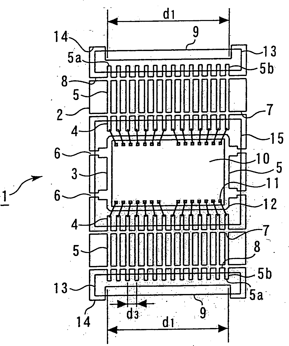
Gemäß einem Gegenstand der vorliegenden Erfindung umfasst ein Zuleitungsrahmen eine Vielzahl von Gerüstzusammenbauten. Jeder Gerüstzusammenbau schließt ein Gerüst, eine Hänge- bzw. Tragzuleitung, deren beide Enden mit dem Gerüst verbunden sind, ein Mikrochipplättchen, welches durch die Tragzuleitung getragen wird und auf den ein Halbleiterchip aufgebracht ist, eine Vielzahl von inneren Zuleitungen, deren Vorderenden über Drähte mit Elektroden auf dem Halbleiterchip verbunden sind, eine Vielzahl von äußeren Zuleitungen, die sich von den Rückenden der Vielzahl von inneren Zuleitungen nach außerhalb des Halbleiterchips erstrecken, wobei die Vorderenden der Vielzahl der äußeren Zuleitungen mit keinen anderen Teilen verbunden sind und in einem freien Zustand verbleiben, einen ersten Steg- bzw. Perforationsstreifen, der in der Nähe der Vielzahl von inneren Zuleitungen quer zur Vielzahl der äußeren Zuleitungen lokalisiert ist, wobei beide Enden des ersten Steg- bzw. Perforationsstreifens mit dem Gerüst verbunden sind, einen zweiten Steg- bzw. Perforationsstreifen, der in der Nähe der Vorderenden der Vielzahl von äußeren Zuleitungen quer zur Vielzahl der äußeren Zuleitungen lokalisiert ist, wobei beide Enden des zweiten Steg- bzw. Perforationsstreifens mit dem Gerüst verbunden sind, und einen Zuleitungsträger ein, welcher aus der Oberfläche des Gerüsts, die auf die Vorderenden der Vielzahl von äußeren Zuleitungen zeigt, zu deren Vorderenden von diesen hin hervorragt und welcher eine rechteckige Form aufweist, deren lange Seiten parallel sind mit zu einer Richtung, in der die Vielzahl der äußeren Zuleitungen eine nach der anderen längsseits angeordnet sind, und deren Länge ungefähr gleich der Länge des Raums ist, der durch alle der Vielzahl von äußeren Zuleitungen belegt ist. Die Vielzahl der Gerüstzusammenbauten sind einer nach dem anderen längsseits in einer Richtung angeordnet, die senkrecht zu der Richtung steht, in der sich die Vielzahl der äußeren Zuleitungen erstreckt. Der Abstand zwischen den am nächsten zueinander ge setzten Zuleitungen von jeweils zwei benachbarten Rahmen ist im wesentlichen das n-fache des Abstands der Vielzahl von äußeren Zuleitungen von jedem Gerüst, wobei n eine ganze Zahl ist.According to an object of the present invention, a lead frame comprises a plurality of scaffold assemblies. Each scaffold assembly includes a scaffold, a hanging or carrying lead, the two ends of which are connected to the scaffolding, a microchip plate which is carried by the carrying lead and on which a semiconductor chip is applied, a large number of inner leads, the front ends of which are connected by wires Electrodes connected on the semiconductor chip are a plurality of outer leads extending from the rear ends of the plurality of inner leads to the outside of the semiconductor chip, the front ends of the plurality of outer leads being connected to no other parts and remaining in a free state, a first web or Perforation strip located near the plurality of inner leads transverse to the plurality of outer leads with both ends of the first web or perforation strip connected to the framework, a second web or perforation strip located near the Leading ends of the plurality of outer leads are located transverse to the plurality of outer leads, both ends of the second web or perforation strip being connected to the framework, and a lead carrier, which extends from the surface of the framework to the front ends of the plurality of shows outer leads, to the front ends of vo protrudes toward the latter and which has a rectangular shape, the long sides of which are parallel to a direction in which the plurality of outer leads are arranged one by one along the length, and the length of which is approximately equal to the length of the space that passes through all the large number of external supply lines is occupied. The plurality of scaffold assemblies are arranged one by one lengthways in a direction perpendicular to the direction in which the plurality of outer leads extend. The distance between the closest to each other set leads of two adjacent frames is essentially n times the distance of the plurality of outer leads from each frame, where n is an integer.
Gemäß einem weiteren Gegenstand der vorliegenden Erfindung wird in einem Verfahren zum Herstellen einer Halbleitervorrichtung ein Zuleitungsrahmen hergestellt. Der Zuleitungsrahmen umfasst eine Vielzahl von Gerüstzusammenbauten. Jeder Gerüstzusammenbau schließt ein Gerüst, eine Tragzuleitung, deren beide Enden mit dem Gerüst verbunden sind, ein Mikrochipplättchen, welches durch die Tragzuleitung getragen wird und auf dem ein Halbleiterchip aufgebracht ist, eine Vielzahl von inneren Zuleitungen, deren Vorderenden über Drähte mit Elektroden auf dem Halbleiterchip verbunden sind, eine Vielzahl von äußeren Zuleitungen, die sich von den Rückenden der Vielzahl von inneren Zuleitungen nach außerhalb des Halbleiterchips erstrecken, wobei die Vorderenden der Vielzahl von äußeren Zuleitungen mit keinem Teil verbunden sind und in einem freien Zustand verbleiben, einen ersten Stegstreifen, der in der Nähe der Vielzahl von inneren Zuleitungen quer zur Vielzahl der äußeren Zuleitungen lokalisiert ist, wobei beide Enden des ersten Stegstreifens mit dem Rahmen verbunden sind, einen zweiten Stegstreifen, der in der Nähe der Vorderenden der Vielzahl von äußeren Zuleitungen quer zur Vielzahl der äußeren Zuleitungen lokalisiert ist, wobei beide Enden des zweiten Stegstreifens mit dem Gerüst verbunden sind, und einen Zuleitungsträger ein, welcher aus der Oberfläche des Rahmens, die auf die Vorderenden der Vielzahl von äußeren Zuleitungen zeigt, zu den Vorderenden von diesen hin hervorragt und welcher eine rechteckige Form besitzt, deren lange Seiten parallel sind zu der Richtung, in welcher die Vielzahl der äußeren Zuleitungen einer nach der anderen längsseits angeordnet sind und deren Länge ungefähr gleich ist zu der Länge des Raums, der durch alle der Vielzahl von äußeren Zuleitungen belegt ist. Die Vielzahl. der Gerüstzusammenbauten sind einer nach dem anderen längsseits in der Richtung angeordnet, die senkrecht zu der Richtung steht, in welcher sich die Vielzahl der äußeren Zuleitungen erstrecken. Der Abstand zwischen am nächsten zueinander gesetzten äußeren Zuleitungen von jeweils zwei benachbarten Gerüsten ist im wesentlichen das n-fache des Abstands der Vielzahl von äußeren Zuleitungen von jedem Rahmen, wobei n eine ganze Zahl ist. Dann wird beim Verfahren zum Herstellen der Halbleitervorrichtung der Halbleiterchip auf das Mikrochipplättchen aufgebracht. Zwischen den Elektroden auf dem Halbleiterchip und der Vielzahl von inneren Zuleitungen werden durch die Drähte elektrische Verbindungen hergestellt. Der Halbleiterchip, das Mikrochipplättchen, die Drähte und die Vielzahl der inneren Zuleitungen werden mit Harz versiegelt bzw. abgedichtet, um eine kleine Vorrichtung zu bilden. Die Vorderenden der Vielzahl von äußeren Zuleitungen und der Zuleitungsträger werden mit dem Harz versiegelt bzw. abgedichtet. Der erste Stegstreifen und der zweite Stegstreifen werden geteilt bzw. geschnitten, um jede der Vielzahl von äußeren Zuleitungen elektrisch zu isolieren. Es wird eine Prüfhilfe verwendet, die eine Vielzahl von Elektrodenterminals aufweist, welche eins nach dem anderen längsseits bei einem Abstand vom im wesentlichen 1/m-fachen des Abstands der Vielzahl der äußeren Zuleitungen von jedem Rahmen angeordnet sind (wobei m eine ganze Zahl ist). Und die Vielzahl der Elektrodenterminals werden mit der Vielzahl der äußeren Zuleitungen verbunden, um die elektrischen Eigenschaften der kleinen Vorrichtung zu prüfen. Die Tragzuleitung wird abgetrennt. Der Zuleitungsträger wird von jedem Gerüst getrennt. Die Vielzahl der äußeren Zuleitungen werden bearbeitet. Der Zuleitungsträger wird abgetrennt.According to another subject of the present invention is in a method of manufacturing a lead frame is fabricated in a semiconductor device. The Lead frame includes a variety of scaffold assemblies. Any scaffolding assembly includes a scaffold, a supporting cable, the two ends of which are connected to the scaffold are a microchip chip, which is carried by the carrying lead and on which a semiconductor chip is applied, a variety of inner leads, the front ends of which are wires with electrodes a large number of external leads are connected on the semiconductor chip, that differ from the backs the large number of inner leads to the outside of the semiconductor chip extend with the front ends of the plurality of outer leads are not connected to any part and remain in a free state, a first land strip that is close to the plurality of inner Leads are located across the multitude of outer leads, wherein both ends of the first web strip are connected to the frame are, a second land strip that is near the front ends of the plurality of external leads across the multitude of outer leads is located, with both ends of the second web strip with the scaffold are connected, and a lead carrier, which from the surface of the Frame on the front ends of the variety of outer leads shows, protruding toward the front ends of these and which one has a rectangular shape, the long sides of which are parallel to the direction in which the plurality of outer leads one after the other the other alongside are arranged and their length approximately the same is to the length the space occupied by all of the large number of external supply lines. The multitude. of the scaffold assemblies one by one alongside arranged in the direction perpendicular to the direction in which the plurality of outer leads extend. The distance between closest outer leads placed against each other of two neighboring scaffolds is essentially that n times the distance of the plurality of outer leads from each Frame, where n is an integer. Then the procedure for Manufacturing the semiconductor device of the semiconductor chip on the Microchip wafer applied. Between the electrodes on the semiconductor chip and The multitude of inner leads are electrical through the wires Connections established. The semiconductor chip, the microchip chip, the wires and the plurality of inner leads are sealed with resin or sealed to form a small device. The front ends the large number of external supply lines and the lead carrier are sealed with the resin. The first web strip and the second land strip are cut to each of the variety of outer leads isolate electrically. A test aid is used, the one Has a variety of electrode terminals, which one after the others alongside at a distance of substantially 1 / m times the distance of the Large number of external supply lines of each frame are arranged (where m is an integer). And the multitude of electrode terminals become with the multitude the outer leads connected to the electrical properties of the small device to consider. The carrying cable is cut off. The lead carrier will from any scaffold Cut. The multitude of external leads are processed. The cable carrier is cut off.
Gemäß einem weiteren Gegenstand der vorliegenden Erfindung wird bei einem Verfahren zum Prüfen der elektrischen Eigenschaften einer Vielzahl von kleinen Vorrichtungen, die durch Aufbringen einer Vielzahl von Halbleiterchips auf einem gemeinsamen Zuleitungsrahmen, Verbinden einer Vielzahl von Zuleitungen zu jedem Halbleiterchip und dann Versiegeln von jedem Halbleiterchip mit Harz gebildet. wurden, eine Prüfhilfe, die eine Vielzahl von bei gleichen Zwischenräumen angeordneten Elektrodenterminals aufweist, derart angeordnet, dass die Richtung, bei der die Vielzahl der Zuleitungen eine nach der anderen längsseits angeordnet sind, parallel zu der Richtung ist, in der die Vielzahl der Elektrodenterminals eines nach dem anderen längsseits angeordnet sind. Die Vielzahl der Elektrodenterminals sind mit der Vielzahl von Zuleitungen verbunden, wobei die Vielzahl der Zuleitungen bei einem Abstand angeordnet sind, der im wesentlichen das n-fache des Abstands der Vielzahl der Elektrodenterminals ist (wobei n eine ganze Zahl ist).According to another aspect of the present invention, in a method for checking the electrical properties of a plurality of small devices by placing a plurality of semiconductor chips on a common lead frame, connecting a plurality of leads to each semiconductor chip, and then sealing each semiconductor chip with resin educated. a test aid, which has a plurality of electrode terminals arranged at the same gaps, arranged in such a way that the direction in which the plurality of leads leads one after the other the other are arranged alongside, is parallel to the direction in which the plurality of electrode terminals are arranged alongside one by one. The plurality of electrode terminals are connected to the plurality of leads, the plurality of leads being arranged at a distance substantially n times the distance of the plurality of electrode terminals (where n is an integer).
Andere und weitere Aufgaben, Merkmale und Vorteile der Erfindung werden aus der nachfolgenden Beschreibung deutlicher.Other and other tasks, characteristics and Advantages of the invention will become apparent from the description below more clear.
Eine bevorzugte Ausführungsform der vorliegenden Erfindung wird unten im Detail unter Bezugnahme auf die beigefügten Zeichnungen beschrieben.A preferred embodiment The present invention is described in detail below on the attached Described drawings.
Die vorliegende Erfindung ist dadurch
gekennzeichnet, dass die Enden
Die vorliegende Erfindung ist auch
dadurch gekennzeichnet, dass die Zuleitungsträger
Die vorliegende Erfindung ist ferner dadurch gekennzeichnet, dass die ersten und zweiten Stegstreifen auf den äußeren Zuleitungen-bereitgestellt werden.The present invention is further characterized in that the first and second Web strips are provided on the outer leads.
In
Gemäß der vorliegenden Erfindung
werden die ersten Stegstreifen
In
Es sollte angemerkt werden, dass dieselbe Prüfhilfe verwendet werden kann zum Messen der elektrischen Eigenschaften einer Vorrichtung, deren äußere Zuleitungen bei einem Abstand angeordnet sind, der das m-fache des Abstands der Elektrodenterminals ist, wobei m eine ganze Zahl ist. Zum Beispiel kann eine Prüfhilfe, die Elektrodenterminals bei einem Abstand von 0,4 mm aufweist, auf Vorrichtungen angewandt werden, deren äußere Zuleitungen bei einem Abstand von nicht nur 0,4 mm, sondern auch von 0,8 mm angeordnet sind. Deshalb braucht die Prüfhilfe nicht gewechselt zu werden, um Vorrichtungen mit unterschiedlichen Pinzahlen, Paketgrößen und Paketbreiten zu prüfen.It should be noted that the same test aid can be used to measure electrical properties a device whose outer leads are arranged at a distance that is m times the distance is the electrode terminal, where m is an integer. For example can be a test aid, has the electrode terminals at a distance of 0.4 mm Devices are used, the outer leads at one Not only 0.4 mm apart, but also 0.8 mm apart are. That is why the testing aid is needed not to be changed to devices with different Pin numbers, package sizes and Check package widths.
Unter Bezugnahme auf
Zuallererst wird ein Zuleitungsrahmen
der vorliegenden Erfindung hergestellt. Zum Beispiel wird, wie in
Unter Bezugnahme auf die
Anschließend werden der Halbleiterchip
Dann werden die ersten Stegstreifen
Um jede Vorrichtung vom Zuleitungsrahmen zu
entfernen, werden somit gemäß der vorliegenden Erfindung
charakteristischer Weise die Zuleitungsträger vom Zuleitungsrahmen abgetrennt
bzw. abgeschnitten, anstatt die äußeren Zuleitungen
abzutrennen bzw. abzuschneiden. Somit sind, wie in
Dann werden bei
Nachfolgend erfolgt eine Beschreibung
eines Verfahrens zum Prüfen
der elektrischen Eigenschaften einer Vorrichtung unter Verwendung
eines Zuleitungsrahmens gemäß der vorliegenden
Erfindung. Wie in
Es sollte angemerkt werden, dass dieselbe Prüfhilfe verwendet werden kann, um die elektrischen Eigenschaften von irgendeiner Vorrichtung zu überprüfen, wenn die Vorrichtung ihre äußeren Zuleitungen bei einem Abstand angeordnet aufweist, der das n-fache des Abstands der Elektrodenterminals darstellt, wobei n eine ganze Zahl ist. Mit anderen Worten ist für einen Zuleitungsrahmen, bei dem der Abstand zwischen den nächstkommenden äußeren Zuleitungen von jeweils zwei benachbarten Vorrichtungen auf das n1-fache des Abstands der äußeren Zuleitungen von jeder Vorrichtung festgelegt ist, möglich, eine Prüfhilfe zu verwenden, deren Elektrodenterminals einen Abstand des 1/n2-fachen des Abstands der äußeren Zuleitungen von jeder Vorrichtung aufweist, wobei n1 und n2 ganze Zahlen sind.It should be noted that the same test tool can be used to test the electrical properties of any device if the device has its outer leads spaced a distance n times the distance of the electrode terminals, where n is an integer is. In other words, for a lead frame in which the distance between the closest outer leads of two adjacent devices is set to n 1 times the distance of the outer leads from each device, it is possible to use a test aid whose electrode terminals are spaced 1 / n 2 times the distance of the outer leads from each device, where n 1 and n 2 are integers.
Zum Beispiel kann eine Prüfhilfe, die bei einem Abstand von 0,4 mm angeordnete Elektrodenterminals aufweist, auf Vorrichtungen angewandt werden, deren äußere Zuleitungen bei einem Abstand von nicht nur 0,4 mm (n2 = 1), sondern auch von 0,8 mm (n2 = 2) angeordnet sind. Es sollte angemerkt werden, dass in diesem Fall der Abstand zwischen den nächstliegenden äußeren Zuleitungen von jeweils zwei benachbarten Vorrichtungen das (0,4 × n1)-fache bzw. das (0,8 × n1)-fache ist. Somit braucht die Prüfhilfe nicht gewechselt zu werden, um Vorrichtungen mit unterschiedlichen Pinzahlen, Paketgrößen, Paketdicken etc. zu prüfen.For example, a test aid, which has electrode terminals arranged at a distance of 0.4 mm, can be applied to devices whose outer leads are not only 0.4 mm (n 2 = 1), but also 0.8 mm (n 2 = 2) are arranged. It should be noted that in this case the distance between the closest outer leads of each two adjacent devices is (0.4 × n 1 ) times or (0.8 × n 1 ) times. This means that the test aid does not need to be changed in order to test devices with different pin numbers, package sizes, package thicknesses, etc.
Ferner wird, wie in
Da die äußeren Zuleitungen durch die Zuleitungsträger getragen und fixiert werden, werden darüber hinaus die äußeren Zuleitungen nicht deformiert, wenn sie mit den Elektrodenterminals in Kontakt gebracht werden, was ebenso zu einer ordentlichen Prüfung führt.Since the outer leads through the lead support the outer leads are also carried and fixed not deformed when in contact with the electrode terminals brought, which also leads to a proper examination.
Es sollte angemerkt werden, dass die obige Beschreibung der vorliegenden Erfindung Ausdrücke wie "das n-fache ..., wobei n eine ganze Zahl ist" und "das m-fache ..., wobei m eine ganze Zahl ist" verwendet. Bei der praktischen Anwendung der vorliegenden Erfindung sollten diese Ausdrücke jedoch als "im wesentlichen das n-fache ..., wobei n eine ganze Zahl ist" und "im wesentlichen das m-fache ..., wobei m einige ganze Zahlen ist" verstanden werden, da eine mathematisch exakte Vervielfachung ganzer Zahlen nicht erforderlich ist. Wenn zum Beispiel die äußeren Zuleitungen von jeder Vorrichtung bei einem Abstand von 0,4 mm angeordnet sind, braucht die anzuwendende Prüfhilfe ihre Elektrodenterminals nicht bei einem Abstand von genau 0,4 mm angeordnet zu haben. Den Elektrodenterminals kann gestattet werden, einen Abstand von ein wenig mehr oder ein wenig weniger als 0,4 mm zu besitzen, wenn bei der Messung kein Problem auftritt. Dieses Prinzip gilt auch für den Abstand zwischen den am nähesten gesetzten äußeren Zuleitungen von jeweils zwei benachbarten Vorrichtungen.It should be noted that the above description of the present invention uses terms such as "n times ... where n is an integer" and "m times ... where m is an integer". However, in the practice of the present invention, these terms should be understood as "substantially n times ... where n is an integer" and "substantially m times ... where m is some integers" because a mathematically exact multiplication of whole numbers is not necessary. If, for example, the outer leads of each device are arranged at a distance of 0.4 mm, the test aid to be used need not have their electrode terminals arranged at a distance of exactly 0.4 mm. The electrode terminals can be allowed be a little more or a little less than 0.4 mm apart if there is no problem with the measurement. This principle also applies to the distance between the closest outer leads of two adjacent devices.
Die oben beschriebene vorliegende
Ausführungsform
wird auf Fälle
angewandt, bei denen jede Vorrichtung in einer einzelnen Reihe in
der Längsrichtung
des Zuleitungsrahmens angeordnet ist. Die vorliegende Erfindung
ist jedoch nicht auf diese spezielle Anordnung beschränkt. Zum
Beispiel kann die vorliegende Erfindung auf eine Anordnung angewandt
werden, bei der eine Vielzahl von Reihen von Vorrichtungen zu der
in
Ferner wird die oben beschriebene vorliegende Ausführungsform auf Halbleitervorrichtungen angewandt, die ein Paket vom SOP-Typ verwenden. Die vorliegende Erfindung ist jedoch nicht auf diese spezielle Art der Halbleitervorrichtung beschränkt. Die vorliegende Erfindung kann auf Halbleitervorrichtungen angewandt werden, die ein Paket vom Typ TSOP (Dünn/Klein-Konturpaket; Thin Small Outline Package) verwenden.Furthermore, the one described above present embodiment applied to semiconductor devices using an SOP type package. The however, the present invention is not limited to this particular type of Semiconductor device limited. The The present invention can be applied to semiconductor devices which are a package of the type TSOP (thin / small contour package; Thin Small Outline Package) use.
Die Merkmale und Vorteile der vorliegenden Erfindung können wie folgt zusammengefasst werden.The features and advantages of the present invention can can be summarized as follows.
Gemäß einem Gegenstand ist es möglich, die elektrischen Eigenschaften einer Vorrichtung in einem Zustand zu prüfen, in dem sie auf einem Zuleitungsrahmen, der eine einzelne Einheit bildet, aufgebracht ist. Da die Zuleitungsträger das Paket und. die äußeren Zuleitungen tragen, kann ferner bei dem Zulei tungsrahmen die Deformation der Tragzuleitungen und der äußeren Zuleitungen reduziert werden.According to an object it is possible to electrical properties of a device in one state check, in which they are on a lead frame that is a single unit forms, is applied. Since the supply carrier the package and. the outer leads can also carry the deformation of the lead frame Carrier cables and the outer cables be reduced.
Gemäß einem weiteren Gegenstand ist es möglich, die zur Prüfung erforderliche Zeit beträchtlich zu mindern sowie das Problem zu lösen, dass die Halbleitervorrichtung von der Prüfhilfe abfallen kann, was zu einer gesteigerten Produktivität führt. Ferner kann dieselbe Prüfhilfe verwendet werden, um Vorrichtungen mit unterschiedlichen Pinzahlen etc. zu prüfen, was zu verminderten Produktionskosten führt.According to another subject Is it possible, those for testing required considerable time mitigate as well as solve the problem that the semiconductor device from the testing aid can drop, which leads to increased productivity. Furthermore, the same test aid used to make devices with different pin numbers etc. to check which leads to reduced production costs.
Gemäß einem weiteren Gegenstand ist es möglich, die elektrischen Eigenschaften (von jeder Vorrichtung) in einem Zustand zu prüfen, in dem sie auf dem Zuleitungsrahmen, der, eine einzelne Einheit bildet, aufgebracht ist, was die zur Prüfung erforderliche Zeit beträchtlich vermindert. Ferner kann dieselbe Prüfhilfe verwendet werden, Vorrichtungen mit unterschiedlichen Pinzahlen etc. zu prüfen.According to another subject Is it possible, the electrical properties (of each device) in one Check condition in which it forms a single unit on the lead frame is upset what the for exam required considerable time reduced. The same test aid can also be used, devices to be checked with different pin numbers etc.
Selbstverständlich sind im Licht der obigen Lehren viele Modifikationen und Variationen der vorliegenden Erfindung möglich. Es ist daher klar, dass innerhalb des Umfangs der beigefügten Ansprüche die Erfindung anders als speziell beschrieben ausgeführt werden kann.Of course, are in the light of the above teachings many modifications and variations of the present invention possible. It is therefore clear that within the scope of the appended claims Invention can be carried out differently than specifically described.
Claims (4)
Applications Claiming Priority (2)
| Application Number | Priority Date | Filing Date | Title |
|---|---|---|---|
| JP2002217694A JP4111767B2 (en) | 2002-07-26 | 2002-07-26 | Manufacturing method of semiconductor device and electrical property inspection method of small element |
| JP2002/217694 | 2002-07-26 |
Publications (1)
| Publication Number | Publication Date |
|---|---|
| DE10306286A1 true DE10306286A1 (en) | 2004-02-12 |
Family
ID=30437653
Family Applications (1)
| Application Number | Title | Priority Date | Filing Date |
|---|---|---|---|
| DE10306286A Ceased DE10306286A1 (en) | 2002-07-26 | 2003-02-14 | Lead frame, method of manufacturing a semiconductor device and method of checking the electrical properties of small devices using the lead frame |
Country Status (6)
| Country | Link |
|---|---|
| US (1) | US6836004B2 (en) |
| JP (1) | JP4111767B2 (en) |
| KR (1) | KR100538020B1 (en) |
| CN (1) | CN1288736C (en) |
| DE (1) | DE10306286A1 (en) |
| TW (1) | TWI224850B (en) |
Families Citing this family (11)
| Publication number | Priority date | Publication date | Assignee | Title |
|---|---|---|---|---|
| JP2004253706A (en) * | 2003-02-21 | 2004-09-09 | Seiko Epson Corp | Lead frame, semiconductor chip packaging member, method of manufacturing semiconductor device, and semiconductor device |
| US7271471B2 (en) * | 2003-06-17 | 2007-09-18 | Dai Nippon Printing Co., Ltd. | Metal substrate apparatus, method of manufacturing an IC card module apparatus, and an IC card module apparatus |
| US7709943B2 (en) | 2005-02-14 | 2010-05-04 | Daniel Michaels | Stacked ball grid array package module utilizing one or more interposer layers |
| US20060202320A1 (en) * | 2005-03-10 | 2006-09-14 | Schaffer Christopher P | Power semiconductor package |
| US20080265248A1 (en) * | 2007-04-27 | 2008-10-30 | Microchip Technology Incorporated | Leadframe Configuration to Enable Strip Testing of SOT-23 Packages and the Like |
| TW200921880A (en) | 2007-11-12 | 2009-05-16 | Orient Semiconductor Elect Ltd | Lead frame structure and applications thereof |
| CN103855119A (en) * | 2012-12-07 | 2014-06-11 | 三垦电气株式会社 | Semiconductor module, semiconductor device and manufacturing method of semiconductor module |
| JP6673012B2 (en) * | 2016-05-26 | 2020-03-25 | 三菱電機株式会社 | Semiconductor device and manufacturing method thereof |
| JP7526980B2 (en) | 2019-10-24 | 2024-08-02 | 日電精密工業株式会社 | Manufacturing method and manufacturing equipment for MAP type lead frame |
| CN111834323B (en) * | 2020-07-29 | 2025-08-19 | 北京燕东微电子科技有限公司 | Semiconductor package and manufacturing method thereof |
| CN118471867B (en) * | 2024-07-13 | 2024-09-24 | 中北大学 | A semiconductor packaging test device and a test method thereof |
Family Cites Families (12)
| Publication number | Priority date | Publication date | Assignee | Title |
|---|---|---|---|---|
| US5541447A (en) * | 1992-04-22 | 1996-07-30 | Yamaha Corporation | Lead frame |
| US5539251A (en) * | 1992-05-11 | 1996-07-23 | Micron Technology, Inc. | Tie bar over chip lead frame design |
| JPH06132464A (en) | 1992-10-15 | 1994-05-13 | Fuji Xerox Co Ltd | Method for assembling semiconductor integrated circuit |
| GB2320964B (en) | 1993-11-25 | 1998-08-26 | Motorola Inc | Method for testing electronic devices attached to a a leadframe |
| KR0145768B1 (en) * | 1994-08-16 | 1998-08-01 | 김광호 | Lead frame and manufacturing method of semiconductor package using same |
| JP2806328B2 (en) * | 1995-10-31 | 1998-09-30 | 日本電気株式会社 | Resin-sealed semiconductor device and method of manufacturing the same |
| JPH09129815A (en) | 1995-11-07 | 1997-05-16 | Hitachi Ltd | Semiconductor device manufacturing method and lead frame used in the manufacturing method |
| JP3420057B2 (en) * | 1998-04-28 | 2003-06-23 | 株式会社東芝 | Resin-sealed semiconductor device |
| JP2000188366A (en) * | 1998-12-24 | 2000-07-04 | Hitachi Ltd | Semiconductor device |
| KR100355796B1 (en) * | 1999-10-15 | 2002-10-19 | 앰코 테크놀로지 코리아 주식회사 | structure of leadframe for semiconductor package and mold for molding the same |
| JP3664045B2 (en) * | 2000-06-01 | 2005-06-22 | セイコーエプソン株式会社 | Manufacturing method of semiconductor device |
| JP3470111B2 (en) * | 2001-06-28 | 2003-11-25 | 松下電器産業株式会社 | Method for manufacturing resin-encapsulated semiconductor device |
-
2002
- 2002-07-26 JP JP2002217694A patent/JP4111767B2/en not_active Expired - Fee Related
-
2003
- 2003-01-15 US US10/342,398 patent/US6836004B2/en not_active Expired - Fee Related
- 2003-02-14 DE DE10306286A patent/DE10306286A1/en not_active Ceased
- 2003-03-19 TW TW092106017A patent/TWI224850B/en not_active IP Right Cessation
- 2003-03-26 KR KR10-2003-0018848A patent/KR100538020B1/en not_active Expired - Fee Related
- 2003-03-27 CN CNB031082971A patent/CN1288736C/en not_active Expired - Fee Related
Also Published As
| Publication number | Publication date |
|---|---|
| US20040018663A1 (en) | 2004-01-29 |
| JP2004063616A (en) | 2004-02-26 |
| JP4111767B2 (en) | 2008-07-02 |
| US6836004B2 (en) | 2004-12-28 |
| CN1471149A (en) | 2004-01-28 |
| KR100538020B1 (en) | 2005-12-21 |
| TWI224850B (en) | 2004-12-01 |
| TW200405537A (en) | 2004-04-01 |
| CN1288736C (en) | 2006-12-06 |
| KR20040010075A (en) | 2004-01-31 |
Similar Documents
| Publication | Publication Date | Title |
|---|---|---|
| DE19712551B4 (en) | Lead frame and chip box semiconductor package manufacturing method applied thereto | |
| DE2858750C2 (en) | ||
| DE19827237B4 (en) | A printed circuit board substrate for a semiconductor device package and a semiconductor device package using the same, and a manufacturing method thereof | |
| DE3884039T2 (en) | Connection method for testing and assembling electronic components. | |
| DE102014106158B4 (en) | Method for testing electronic components and semiconductor strip assembly | |
| DE10306286A1 (en) | Lead frame, method of manufacturing a semiconductor device and method of checking the electrical properties of small devices using the lead frame | |
| DE69628964T2 (en) | Resin molded semiconductor device and manufacturing process | |
| DE19743537A1 (en) | Semiconductor package for surface mounting and method for its production | |
| DE10014620A1 (en) | Method for producing a carrier tape with a plurality of electrical units, each comprising a chip and contact elements | |
| DE69305633T2 (en) | Method and device for connecting wires between a semiconductor chip and the associated lead frame | |
| DE2855838A1 (en) | CARRIER STRIP FOR ROUND CONNECTOR PINS AND METHOD FOR MANUFACTURING CARRIER STRIPS | |
| DE19651549B4 (en) | Connection frame and chip housing | |
| DE10153666A1 (en) | High density contact arrangement for integrated circuit chips has diagonal layout to reduce separation | |
| EP3048653B1 (en) | Method of making current sensors | |
| EP1413184B1 (en) | Method for testing a chip with a housing and for placing said housing on the board | |
| DE19931278B4 (en) | Test card and IC tester | |
| DE102013018518A1 (en) | IC module for different connection techniques | |
| DE102013200944A1 (en) | A method of manufacturing a semiconductor device and semiconductor device | |
| DE112018005048T5 (en) | INTEGRATED CIRCUIT (IC) CHIP MOUNTED BETWEEN AN OFFSET FRAME CHIP MOUNTING PAD AND A DISCRETE CHIP MOUNTING PAD | |
| DE10057412A1 (en) | Semiconductor device encapsulation arrangement and method for its production | |
| DE102015118631B4 (en) | Method for forming and processing lead frame strips with molding compound channels and housing arrangements comprising these | |
| DE2303537A1 (en) | CONNECTING RAIL AND METHOD OF MANUFACTURING IT | |
| DE10310536B4 (en) | Semiconductor device and manufacturing method therefor | |
| WO1989008265A1 (en) | Device for testing printed circuit boards | |
| DE3614087A1 (en) | DEVICE AND METHOD FOR IMPROVED ENCLOSURE OF SEMICONDUCTOR DEVICES |
Legal Events
| Date | Code | Title | Description |
|---|---|---|---|
| OP8 | Request for examination as to paragraph 44 patent law | ||
| 8131 | Rejection |