DE10230674B4 - Semiconductor capacitor and thus constructed MOSFET - Google Patents
Semiconductor capacitor and thus constructed MOSFET Download PDFInfo
- Publication number
- DE10230674B4 DE10230674B4 DE10230674A DE10230674A DE10230674B4 DE 10230674 B4 DE10230674 B4 DE 10230674B4 DE 10230674 A DE10230674 A DE 10230674A DE 10230674 A DE10230674 A DE 10230674A DE 10230674 B4 DE10230674 B4 DE 10230674B4
- Authority
- DE
- Germany
- Prior art keywords
- capacitor
- semiconductor
- dielectric
- electrode
- praseodymium
- Prior art date
- Legal status (The legal status is an assumption and is not a legal conclusion. Google has not performed a legal analysis and makes no representation as to the accuracy of the status listed.)
- Expired - Fee Related
Links
Classifications
-
- H10P14/6334—
-
- H—ELECTRICITY
- H10—SEMICONDUCTOR DEVICES; ELECTRIC SOLID-STATE DEVICES NOT OTHERWISE PROVIDED FOR
- H10D—INORGANIC ELECTRIC SEMICONDUCTOR DEVICES
- H10D1/00—Resistors, capacitors or inductors
- H10D1/60—Capacitors
- H10D1/62—Capacitors having potential barriers
- H10D1/66—Conductor-insulator-semiconductor capacitors, e.g. MOS capacitors
-
- H—ELECTRICITY
- H10—SEMICONDUCTOR DEVICES; ELECTRIC SOLID-STATE DEVICES NOT OTHERWISE PROVIDED FOR
- H10D—INORGANIC ELECTRIC SEMICONDUCTOR DEVICES
- H10D1/00—Resistors, capacitors or inductors
- H10D1/60—Capacitors
- H10D1/68—Capacitors having no potential barriers
- H10D1/692—Electrodes
-
- H10D64/0134—
-
- H—ELECTRICITY
- H10—SEMICONDUCTOR DEVICES; ELECTRIC SOLID-STATE DEVICES NOT OTHERWISE PROVIDED FOR
- H10D—INORGANIC ELECTRIC SEMICONDUCTOR DEVICES
- H10D64/00—Electrodes of devices having potential barriers
- H10D64/60—Electrodes characterised by their materials
- H10D64/66—Electrodes having a conductor capacitively coupled to a semiconductor by an insulator, e.g. MIS electrodes
- H10D64/68—Electrodes having a conductor capacitively coupled to a semiconductor by an insulator, e.g. MIS electrodes characterised by the insulator, e.g. by the gate insulator
- H10D64/681—Electrodes having a conductor capacitively coupled to a semiconductor by an insulator, e.g. MIS electrodes characterised by the insulator, e.g. by the gate insulator having a compositional variation, e.g. multilayered
- H10D64/685—Electrodes having a conductor capacitively coupled to a semiconductor by an insulator, e.g. MIS electrodes characterised by the insulator, e.g. by the gate insulator having a compositional variation, e.g. multilayered being perpendicular to the channel plane
-
- H—ELECTRICITY
- H10—SEMICONDUCTOR DEVICES; ELECTRIC SOLID-STATE DEVICES NOT OTHERWISE PROVIDED FOR
- H10D—INORGANIC ELECTRIC SEMICONDUCTOR DEVICES
- H10D64/00—Electrodes of devices having potential barriers
- H10D64/60—Electrodes characterised by their materials
- H10D64/66—Electrodes having a conductor capacitively coupled to a semiconductor by an insulator, e.g. MIS electrodes
- H10D64/68—Electrodes having a conductor capacitively coupled to a semiconductor by an insulator, e.g. MIS electrodes characterised by the insulator, e.g. by the gate insulator
- H10D64/691—Electrodes having a conductor capacitively coupled to a semiconductor by an insulator, e.g. MIS electrodes characterised by the insulator, e.g. by the gate insulator comprising metallic compounds, e.g. metal oxides or metal silicates
-
- H—ELECTRICITY
- H10—SEMICONDUCTOR DEVICES; ELECTRIC SOLID-STATE DEVICES NOT OTHERWISE PROVIDED FOR
- H10D—INORGANIC ELECTRIC SEMICONDUCTOR DEVICES
- H10D64/00—Electrodes of devices having potential barriers
- H10D64/60—Electrodes characterised by their materials
- H10D64/66—Electrodes having a conductor capacitively coupled to a semiconductor by an insulator, e.g. MIS electrodes
- H10D64/68—Electrodes having a conductor capacitively coupled to a semiconductor by an insulator, e.g. MIS electrodes characterised by the insulator, e.g. by the gate insulator
- H10D64/693—Electrodes having a conductor capacitively coupled to a semiconductor by an insulator, e.g. MIS electrodes characterised by the insulator, e.g. by the gate insulator the insulator comprising nitrogen, e.g. nitrides, oxynitrides or nitrogen-doped materials
-
- H10P14/6506—
-
- H10P14/662—
-
- H10P14/6933—
-
- H10P14/69396—
-
- H10D64/01342—
Landscapes
- Semiconductor Integrated Circuits (AREA)
- Metal-Oxide And Bipolar Metal-Oxide Semiconductor Integrated Circuits (AREA)
Abstract
Halbleiterkondensator mit einer ersten Kondensatorelektrode (1; 10), einer zweiten Kondensatorelektrode (3; 30) und einem zwischen den beiden Kondensatorelektroden (1, 3; 10, 30) angeordneten Kondensatordielektrikum (5; 50), das Praseodymoxid umfasst, wobei die zweite Kondensatorelektrode (3; 30) Praseodymsilizid umfasst und die erste Kondensatorelektrode (1; 10) eine Siliziumgermaniumlegierung umfasst.Semiconductor capacitor with a first capacitor electrode (1; 10), a second capacitor electrode (3; 30) and one between the two capacitor electrodes (1, 3; 10, 30) arranged capacitor dielectric (5; 50), the praseodymium oxide wherein the second capacitor electrode (3; 30) comprises praseodymium silicide and the first capacitor electrode (1; 10) is a silicon germanium alloy includes.
Description
Die Erfindung betrifft einen Halbleiterkondensator mit einem zwischen einer ersten Kondensatorelektrode und einer zweiten Kondensatorelektrode angeordneten Kondensatordielektrikum, das Praseodymoxid umfasst, sowie einen mit einem solchen Halbleiterkondensator aufgebauten MOSFET.The The invention relates to a semiconductor capacitor with an intermediate a first capacitor electrode and a second capacitor electrode arranged Capacitor dielectric comprising praseodymium oxide, as well as a constructed with such a semiconductor capacitor MOSFET.
Halbleiterkondensatoren sind aus der modernen Halbleitertechnologie nicht mehr wegzudenken. Wichtige Anwendungsbeispiele für Halbleiterkondensatoren sind dynamische Direktzugriffsspeicher (DRAM), in denen die Halbleiterkondensatoren als Speicherzellen Verwendung finden, und Metall-Oxid-Halbleiter-Feldeffekttransistoren (MOSFETs, metal-oxide semiconductor field-effect transistor), in denen das Substrat, die Gateelektrode und das zwischen Substrat und Gateelektrode liegende Gateoxid einen Halbleiterkondensator bilden.Semiconductor capacitors are an indispensable part of modern semiconductor technology. Important application examples for Semiconductor capacitors are Dynamic Random Access Memory (DRAM), in which the semiconductor capacitors use as memory cells find, and metal oxide semiconductor field effect transistors (MOSFETs, metal oxide semiconductor field-effect transistor), in which the substrate, the gate electrode and the gate oxide between substrate and gate electrode form a semiconductor capacitor.
Für einen Halbleiterkondensator gilt wie für alle Kondensatoren, dass die Kapazität des Kondensators proportional zur Dielektrizitätszahl des zwischen den Kondensatorelektroden befindlichen Dielektrikums und der Fläche der Kondensatorelektroden sowie zum Reziprokenwert des Abstandes zwischen den Kondensatorelektroden, also der Dicke des Dielektrikums, ist. Als Dielektrikum wird in der Halbleitertechnik häufig Siliziumoxid (SiO2) eingesetzt.For a semiconductor capacitor as for all capacitors, the capacitance of the capacitor is proportional to the dielectric constant of the dielectric located between the capacitor electrodes and the area of the capacitor electrodes and to the reciprocal of the distance between the capacitor electrodes, ie the thickness of the dielectric. Silicon dioxide (SiO 2 ) is frequently used as the dielectric in semiconductor technology.
Mit der zunehmenden Verringerung der Bausteingröße in der Halbleitertechnik werden auch die Abmessungen der Kondensatorplatten von Halbleiterkondensatoren, beispielsweise der Gateelektroden von MOSFETs, immer kleiner. Damit verringert sich aber auch die Kapazität des Halbleiterkondensators, sofern keine Maßnahmen ergriffen werden, dem entgegenzuwirken.With the increasing reduction of the size of chips in semiconductor technology also the dimensions of the capacitor plates of semiconductor capacitors, For example, the gate electrodes of MOSFETs, smaller and smaller. In order to but also reduces the capacity of the semiconductor capacitor, provided no action be taken to counteract this.
Zum Kompensieren der Verringerung der Abmessungen der Kondensatorelektroden gibt es zwei Möglichkeiten. Die erste besteht darin, die Dicke des Dielektrikums zu verringern. Dies führt beispielsweise in MOSFETs, in denen als Dielektrikum typischerweise Siliziumoxid Verwendung findet, bei Gatelängen von weniger als 0,1 μm zu Problemen. Das Siliziumoxid für Bauelemente mit derart geringen Gatelängen müsste dann dünner als 1,5 nm sein. Ein solch dünnes Siliziumoxid führt jedoch zu einer Zunahme des Leckstroms des MOSFETs. Der Leckstrom entsteht aufgrund von Elektronen, die durch das dünne Gateoxid zwischen dem Substrat und der Gateelektrode tunneln. Die Zahl der tunnelnden Elektronen und damit die Stromstärke des Leckstroms wächst exponentiell mit geringer werdender Dicke der Siliziumoxidschicht. Es ist jedoch erwünscht, den Leckstrom eines MOSFETs möglichst gering zu halten, da zum Steuern des Stromes zwischen der Drainelektrode und der Sourceelektrode möglichst wenig elektrische Leistung verbraucht werden soll.To the Compensating the reduction in the dimensions of the capacitor electrodes There are two options. The first is to reduce the thickness of the dielectric. this leads to For example, in MOSFETs where typically used as a dielectric Silicon oxide is used, with gate lengths of less than 0.1 microns to problems. The Silica for Components with such low gate lengths would then have to be thinner than 1.5 nm. Such a thin Silica leads however, an increase in the leakage current of the MOSFET. The leakage current is due to electrons passing through the thin gate oxide tunnel between the substrate and the gate electrode. The number of Tunneling electrons and thus the current strength of the leakage current grows exponentially with decreasing thickness of the silicon oxide layer. However, it is he wishes, the leakage current of a MOSFET as possible to keep low because to control the current between the drain electrode and the source electrode as possible low electrical power is to be consumed.
Eine
weitere Möglichkeit,
die Verringerung der Abmessungen der Kondensatorelektroden zu kompensieren
besteht darin, die Dielektrizitätszahl des
Dielektrikums zu ändern.
Wird statt Siliziumoxid Praseodymoxid (Pr2O3) als Dielektrikum verwendet wie z.B. in
der
An das Praseodymoxid umfassende Kondensatordielektrikum schließt sich eine Kondensatorelektrode an, die üblicherweise Silizium umfasst. Diese wird wiederum über eine Metallsilizidschicht elektrisch kontaktiert. Zwischen dem Kondensatordielektrikum und der Kondensatorelektrode befindet sich darüber hinaus noch eine Zwischenschicht zum Unterdrücken chemischer Reaktionen zwischen dem Material des Kondensatordielektrikums und dem der Kondensatorelektrode.At the praseodymium oxide-containing capacitor dielectric closes a capacitor electrode, which usually comprises silicon. This will turn over electrically contacting a metal silicide layer. Between the capacitor dielectric and the capacitor electrode is also still an intermediate layer to suppress chemical reactions between the material of the capacitor dielectric and the capacitor electrode.
Aufgabe der Erfindung ist es, einen Halbleiterkondensator mit Praseodymoxid als Kondensatordielektrikum sowie einen mit einem solchen Halbleiterkondensator aufgebauten MOSFET zu schaffen, der einen gegenüber dem Stand der Technik einfacheren Aufbau aufweist.task The invention is a semiconductor capacitor with praseodymium oxide as a capacitor dielectric and one with such a semiconductor capacitor to provide a built MOSFET, the simpler compared to the prior art Structure has.
Diese Aufgabe wird durch einen Halbleiterkondensator nach Anspruch 1 und einen MOSFET nach Anspruch 3 gelöst. Der abhängige Anspruch enthält eine weitere vorteilhafte Ausgestaltung des Halbleiterkondensators.These The object is achieved by a semiconductor capacitor according to claim 1 and a MOSFET according to claim 3 solved. The dependent Claim contains a further advantageous embodiment of the semiconductor capacitor.
Erfindungsgemäß umfasst der Halbleiterkondensator eine erste Kondensatorelektrode, eine zweite Kondensatorelektrode sowie ein zwischen den beiden Kondensatorelektroden angeordnetes Kondensatordielektrikum, das Praseodymoxid umfasst. Er zeichnet sich dadurch aus, dass die zweite Kondensatorelektrode Praseodymsilizid und die erste Kondensatorelektrode eine Siliziumgermaniumlegierung umfasst.According to the invention the semiconductor capacitor has a first capacitor electrode, a second capacitor Capacitor electrode and one between the two capacitor electrodes arranged capacitor dielectric comprising praseodymium oxide. It is characterized in that the second capacitor electrode Praseodymium silicide and the first capacitor electrode is a silicon germanium alloy includes.
Der Vorteil dieser Lösung besteht darin, dass sowohl das Material des Kondensatordielektrikums als auch das Material der zweiten Kondensatorelektrode Praseodym enthält, also eine gewisse chemische Verwandtschaft zwischen den beiden Materialien besteht. Aufgrund dieser Verwandtschaft ist die Zwischenschicht zwischen dem Kondensatordielektrikum und der Kondensatorelektrode entbehrlich.Of the Advantage of this solution is that both the material of the capacitor dielectric as Also contains the material of the second capacitor electrode praseodymium, ie a certain chemical relationship between the two materials consists. Because of this relationship is the intermediate layer between the capacitor dielectric and the capacitor electrode dispensable.
In einer weiteren Ausgestaltung besteht die gesamte zweite Kondensatorelektrode des erfindungsgemäßen Halbleiterkondensators vollständig aus Praseodymsilizid. In dieser Ausgestaltung ist keine zusätzliche Kontaktsilizidschicht nötig, da das Praseodymsilizid selbst als Kontaktsilizid fungiert. Daher ermöglicht diese Ausgestaltung einen besonders einfachen Aufbau des Halbleiterkondensators.In In a further embodiment, the entire second capacitor electrode the semiconductor capacitor according to the invention completely off Praseodymium. In this embodiment is no additional Contact silicide layer necessary, since the praseodymium silicide itself acts as a contact silicide. Therefore allows this embodiment a particularly simple structure of the semiconductor capacitor.
Gemäß einem weiteren Aspekt der Erfindung wird ein MOSFET zur Verfügung gestellt, der ein Halbleitersubstrat, ein Gatedielektrikum und eine Gateelektrode als einen erfindungsgemäßen Halbleiterkondensator umfasst. Dabei wird die erste Kondensatorelektrode vom Halbleitersubstrat, die zweite Kondensatorelektrode von der Gateelektrode und das Kondensatordielektrikum vom Gatedielektrikum gebildet.According to one Another aspect of the invention provides a MOSFET, a semiconductor substrate, a gate dielectric, and a gate electrode as a semiconductor capacitor according to the invention includes. In this case, the first capacitor electrode from the semiconductor substrate, the second capacitor electrode from the gate electrode and the capacitor dielectric formed by the gate dielectric.
Weitere vorteilhafte Ausgestaltungen des erfindungsgemäßen Halbleiterkondensators sowie des erfindungsgemäßen MOSFETs werden nachfolgend anhand von Ausführungsbeispielen unter Zuhilfenahme der beigefügten Zeichnungen erläutert.Further advantageous embodiments of the semiconductor capacitor according to the invention and the MOSFET according to the invention will be described below with reference to exemplary embodiments with the aid the attached Drawings explained.
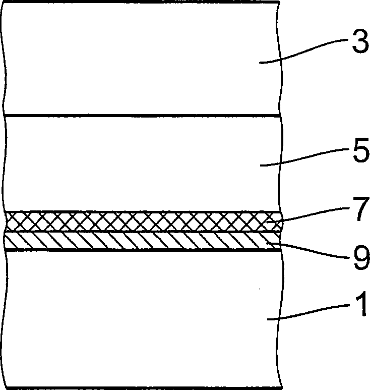
In
Die
Praseodymsilizidschicht
Wenn
der Halbleiterbereich
Ein
Ausführungsbeispiel
für den
erfindungsgemäßen MOSFET
ist in
Statt einem Siliziumsubstrat weist der MOSFET ein Halbleitersubstrat auf, das eine Siliziumgermaniumlegierung umfasst. Das Halbleitersubstrat kann aber alternativ auch vollständig aus der Siliziumgermaniumlegierung bestehen.Instead of a silicon substrate, the MOSFET has a semiconductor substrate, which comprises a silicon germanium alloy. The semiconductor substrate can but alternatively completely consist of the silicon germanium alloy.
Zwar
ist das Halbleitersubstrat
Claims (3)
Priority Applications (3)
| Application Number | Priority Date | Filing Date | Title |
|---|---|---|---|
| DE10230674A DE10230674B4 (en) | 2002-07-04 | 2002-07-04 | Semiconductor capacitor and thus constructed MOSFET |
| US10/520,396 US7060600B2 (en) | 2002-07-04 | 2003-07-04 | Semiconductor capacitor and MOSFET fitted therewith |
| PCT/EP2003/007179 WO2004006315A2 (en) | 2002-07-04 | 2003-07-04 | Semiconductor capacitor and mosfet fitted therewith |
Applications Claiming Priority (1)
| Application Number | Priority Date | Filing Date | Title |
|---|---|---|---|
| DE10230674A DE10230674B4 (en) | 2002-07-04 | 2002-07-04 | Semiconductor capacitor and thus constructed MOSFET |
Publications (2)
| Publication Number | Publication Date |
|---|---|
| DE10230674A1 DE10230674A1 (en) | 2004-01-22 |
| DE10230674B4 true DE10230674B4 (en) | 2006-11-23 |
Family
ID=29761731
Family Applications (1)
| Application Number | Title | Priority Date | Filing Date |
|---|---|---|---|
| DE10230674A Expired - Fee Related DE10230674B4 (en) | 2002-07-04 | 2002-07-04 | Semiconductor capacitor and thus constructed MOSFET |
Country Status (3)
| Country | Link |
|---|---|
| US (1) | US7060600B2 (en) |
| DE (1) | DE10230674B4 (en) |
| WO (1) | WO2004006315A2 (en) |
Families Citing this family (5)
| Publication number | Priority date | Publication date | Assignee | Title |
|---|---|---|---|---|
| EP1396028A2 (en) * | 2001-05-26 | 2004-03-10 | IHP GmbH-Innovations for High Performance Microelectronics/Institut für innovative Mikroelektronik | Transistor, method for producing an integrated circuit and method for producing a metal silicide layer |
| DE10340202A1 (en) * | 2003-08-28 | 2005-04-14 | IHP GmbH - Innovations for High Performance Microelectronics/Institut für innovative Mikroelektronik | Manufacturing Method for Semiconductor Device with Praseodymium Oxide Dielectric |
| WO2005092981A1 (en) * | 2004-03-26 | 2005-10-06 | Kaneka Corporation | Composition curable by both free-radical photocuring and cationic photocuring |
| DE102005051573B4 (en) * | 2005-06-17 | 2007-10-18 | IHP GmbH - Innovations for High Performance Microelectronics/Institut für innovative Mikroelektronik | MIM / MIS structure with praseodymium titanate as insulator material |
| GB2534191A (en) * | 2015-01-16 | 2016-07-20 | Mahle Int Gmbh | Sliding bearing |
Citations (2)
| Publication number | Priority date | Publication date | Assignee | Title |
|---|---|---|---|---|
| DE10039327A1 (en) * | 2000-08-03 | 2002-02-14 | Ihp Gmbh | Electronic component and manufacturing method for electronic component |
| DE10127234A1 (en) * | 2001-05-26 | 2002-12-05 | Ihp Gmbh | Transistor, used as a MOS transistor, has a contact region containing praseodymium silicide between a semiconductor region and a metallic conducting region |
Family Cites Families (9)
| Publication number | Priority date | Publication date | Assignee | Title |
|---|---|---|---|---|
| US5366833A (en) * | 1993-03-22 | 1994-11-22 | Shaw Joel F | Security documents |
| US5356833A (en) * | 1993-04-05 | 1994-10-18 | Motorola, Inc. | Process for forming an intermetallic member on a semiconductor substrate |
| JP2616741B2 (en) * | 1995-04-27 | 1997-06-04 | 日本電気株式会社 | Method for manufacturing polycrystalline silicon-germanium thin film transistor |
| US20020036313A1 (en) | 2000-06-06 | 2002-03-28 | Sam Yang | Memory cell capacitor structure and method of formation |
| US20050145959A1 (en) * | 2001-03-15 | 2005-07-07 | Leonard Forbes | Technique to mitigate short channel effects with vertical gate transistor with different gate materials |
| EP1396028A2 (en) * | 2001-05-26 | 2004-03-10 | IHP GmbH-Innovations for High Performance Microelectronics/Institut für innovative Mikroelektronik | Transistor, method for producing an integrated circuit and method for producing a metal silicide layer |
| US6656852B2 (en) | 2001-12-06 | 2003-12-02 | Texas Instruments Incorporated | Method for the selective removal of high-k dielectrics |
| US6900122B2 (en) | 2001-12-20 | 2005-05-31 | Micron Technology, Inc. | Low-temperature grown high-quality ultra-thin praseodymium gate dielectrics |
| US7205218B2 (en) | 2002-06-05 | 2007-04-17 | Micron Technology, Inc. | Method including forming gate dielectrics having multiple lanthanide oxide layers |
-
2002
- 2002-07-04 DE DE10230674A patent/DE10230674B4/en not_active Expired - Fee Related
-
2003
- 2003-07-04 WO PCT/EP2003/007179 patent/WO2004006315A2/en not_active Ceased
- 2003-07-04 US US10/520,396 patent/US7060600B2/en not_active Expired - Fee Related
Patent Citations (2)
| Publication number | Priority date | Publication date | Assignee | Title |
|---|---|---|---|---|
| DE10039327A1 (en) * | 2000-08-03 | 2002-02-14 | Ihp Gmbh | Electronic component and manufacturing method for electronic component |
| DE10127234A1 (en) * | 2001-05-26 | 2002-12-05 | Ihp Gmbh | Transistor, used as a MOS transistor, has a contact region containing praseodymium silicide between a semiconductor region and a metallic conducting region |
Non-Patent Citations (2)
| Title |
|---|
| MÜSSIG, H.-J., u.a.: "Can Praseodymium Oxide be an Alternative High-K Gate Dielectric Material for Silicon Integrated Circuits ?" In: IEEE Integrated Reliability Workshop Final Report, 2001, S. 1-10 |
| MÜSSIG, H.-J., u.a.: "Can Praseodymium Oxide be anAlternative High-K Gate Dielectric Material for Silicon Integrated Circuits ?" In: IEEE IntegratedReliability Workshop Final Report, 2001, S. 1-10 * |
Also Published As
| Publication number | Publication date |
|---|---|
| DE10230674A1 (en) | 2004-01-22 |
| WO2004006315A3 (en) | 2004-05-27 |
| US7060600B2 (en) | 2006-06-13 |
| WO2004006315A2 (en) | 2004-01-15 |
| US20050212030A1 (en) | 2005-09-29 |
Similar Documents
| Publication | Publication Date | Title |
|---|---|---|
| DE69021419T2 (en) | Semiconductor memory device with a ferroelectric material. | |
| DE19727466C2 (en) | DRAM cell arrangement and method for its production | |
| DE69530716T2 (en) | Accelerometer and method of making the same | |
| DE102010062721A1 (en) | Semiconductor device with improved on-resistance | |
| DE2810597A1 (en) | ELECTRICAL COMPONENT STRUCTURE WITH A MULTI-LAYER INSULATING LAYER | |
| DE3247197A1 (en) | ELECTRICALLY PROGRAMMABLE AND CLEARABLE STORAGE CELL | |
| DE3236469C2 (en) | ||
| EP1294021A1 (en) | Capacitor device for a semiconductor circuit arrangement and method for making the same | |
| DE19946437A1 (en) | Ferroelectric transistor | |
| DE3122437A1 (en) | METHOD FOR PRODUCING A MOS COMPONENT | |
| DE10135557A1 (en) | Semiconductive device used in complementary metal oxide semiconductor transistor, sequentially comprises substrate, conductive silicon film, silicide film, barrier film, and metal film | |
| EP1145319B1 (en) | Integrated circuit and method for the production thereof | |
| DE10341062A1 (en) | Gate structure of non-volatile integrated circuit memory device, comprises thermal oxidation layer defining sidewall of gate structure, oxygen diffusion barrier layer on the sidewall, and floating gate with curved sidewall portion | |
| DE19923388A1 (en) | Semiconductor memory component with SOI (silicon on insulator) structure and method for its production | |
| DE19857038A1 (en) | FEMFET device and method for its production | |
| DE10230674B4 (en) | Semiconductor capacitor and thus constructed MOSFET | |
| EP0207486A1 (en) | Integrated circuit containing MOS transistors and comprising a gate metallization of a metal or a metal silicide of the elements tantalum or niobium, as well as a method of producing this gate metallization | |
| DE112014000641T5 (en) | Semiconductor device and method for its production | |
| DE60030386T2 (en) | Method of Making Field Effect Devices and Thin Film Dielectric Capacities and Devices so Produced | |
| DE10306315B4 (en) | Semiconductor device and corresponding manufacturing method | |
| EP1181723A1 (en) | Double gate mosfet transistor and method for the production thereof | |
| DE10164741A1 (en) | Multiple deposition of metal layers to produce the upper capacitor electrode of a trench capacitor | |
| DE4140173C2 (en) | DRAM and method for its production | |
| DE69029485T2 (en) | Metal oxide semiconductor device and manufacturing method | |
| EP0417341B1 (en) | Capacitor structure for field-effect transistor semiconductor memories |
Legal Events
| Date | Code | Title | Description |
|---|---|---|---|
| OP8 | Request for examination as to paragraph 44 patent law | ||
| 8364 | No opposition during term of opposition | ||
| 8327 | Change in the person/name/address of the patent owner |
Owner name: IHP GMBH - INNOVATIONS FOR HIGH PERFORMANCE MI, DE |
|
| 8339 | Ceased/non-payment of the annual fee |