PRIORITÄTSANSPRUCHPRIORITY CLAIM
Diese Anmeldung beansprucht die Priorität der am 5. März 2020 eingereichten vorläufigen US-Anmeldung Nr. 62/985,391 , die hiermit durch Bezugnahme in vollem Umfang in den vorliegenden Text aufgenommen wird.This application claims priority to U.S. Provisional Application No. 62 / 985,391 , which is hereby incorporated into the present text in its entirety by reference.
HINTERGRUNDBACKGROUND
Die Branche der integrierten Halbleiterschaltkreise (Integrated Circuits, ICs) hat eine breite Vielzahl verschiedener digitaler Vorrichtungen produziert, um Probleme in einer Reihe verschiedener Bereiche zu lösen. Der jüngste Trend zur Miniaturisierung von ICs hat zu kleineren Vorrichtungen geführt, die weniger Strom verbrauchen und dennoch mehr Funktionalität bei höheren Geschwindigkeiten bieten. Der Miniaturisierungsprozess hat auch zu strengeren Design- und Herstellungsspezifikationen sowie zu Herausforderungen hinsichtlich der Zuverlässigkeit geführt. Verschiedene Electronic Design Automation-Tools (EDA-Tools) generieren, optimieren und verifizieren Standardzellenlayout-Designs für integrierte Schaltkreise und stellen dabei sicher, dass die Layout-Designs und Herstellungsspezifikationen eingehalten werden.The semiconductor integrated circuit (IC) industry has produced a wide variety of different digital devices to solve problems in a number of different areas. The recent trend towards miniaturization of ICs has resulted in smaller devices that consume less power yet offer more functionality at higher speeds. The miniaturization process has also resulted in more stringent design and manufacturing specifications, as well as reliability challenges. Various Electronic Design Automation (EDA) tools generate, optimize and verify standard cell layout designs for integrated circuits while ensuring that the layout designs and manufacturing specifications are adhered to.
FigurenlisteFigure list
Aspekte der vorliegenden Offenbarung werden am besten anhand der folgenden detaillierten Beschreibung verstanden, wenn sie zusammen mit den begleitenden Figuren gelesen wird. Es ist anzumerken, dass gemäß der gängigen Praxis in der Industrie verschiedene Merkmale nicht maßstabsgetreu gezeichnet sind. Die Abmessungen der verschiedenen Merkmale können vielmehr im Interesse der Übersichtlichkeit der Besprechung nach Bedarf vergrößert oder verkleinert werden.
- 1 ist ein Schaubild eines Layout-Designs gemäß einigen Ausführungsformen.
- 2A-2B sind Schaubilder eines Layout-Designs eines integrierten Schaltkreises gemäß einigen Ausführungsformen.
- 3A-3B sind Schaubilder einer Draufsicht auf einen integrierten Schaltkreis gemäß einigen Ausführungsformen.
- 4A-4B sind perspektivische Ansichten von FinFETs gemäß einigen Ausführungsformen.
- 5A-5B sind Schaubilder eines Layout-Designs gemäß einigen Ausführungsformen.
- 6A-6B sind Schaubilder einer Draufsicht auf einen integrierten Schaltkreis gemäß einigen Ausführungsformen.
- 7A-7B sind Schaubilder eines Layout-Designs gemäß einigen Ausführungsformen.
- 8A-8B sind Schaubilder einer Draufsicht auf einen integrierten Schaltkreis gemäß einigen Ausführungsformen.
- 9A-9C sind schematische Ansichten von Layout-Designs integrierter Schaltkreise gemäß einigen Ausführungsformen.
- 10A-10E sind schematische Ansichten von Layout-Designs integrierter Schaltkreise gemäß einigen Ausführungsformen.
- 11 ist ein Funktionsflussdiagramm mindestens eines Abschnitts eines Designs- und Herstellungsflusses für integrierte Schaltkreise gemäß einigen Ausführungsformen.
- 12A ist ein Schaltplan eines integrierten Schaltkreises gemäß einigen Ausführungsformen.
- 12B ist ein Schaltplan eines integrierten Schaltkreises gemäß einigen Ausführungsformen.
- 13 ist eine schematische Ansicht eines Systems zum Entwerfen eines IC-Layout-Designs und zur Herstellung eines ICs gemäß einigen Ausführungsformen.
- 14 ist ein Blockschaubild eines Herstellungssystems für integrierte Schaltkreise (ICs) und eines damit verbundenen IC-Herstellungsflusses gemäß einigen Ausführungsformen.
Aspects of the present disclosure are best understood from the following detailed description when read in conjunction with the accompanying figures. It should be noted that, in accordance with common industry practice, various features are not drawn to scale. Rather, the dimensions of the various features can be increased or decreased as needed for clarity of the meeting. - 1 FIG. 3 is a diagram of a layout design in accordance with some embodiments.
- 2A-2B 14 are diagrams of a layout design of an integrated circuit in accordance with some embodiments.
- 3A-3B 14 are diagrams of a top view of an integrated circuit in accordance with some embodiments.
- 4A-4B Figure 4 is perspective views of FinFETs in accordance with some embodiments.
- 5A-5B 13 are diagrams of a layout design in accordance with some embodiments.
- 6A-6B 14 are diagrams of a top view of an integrated circuit in accordance with some embodiments.
- 7A-7B 13 are diagrams of a layout design in accordance with some embodiments.
- 8A-8B 14 are diagrams of a top view of an integrated circuit in accordance with some embodiments.
- 9A-9C 14 are schematic views of integrated circuit layout designs in accordance with some embodiments.
- 10A-10E 14 are schematic views of integrated circuit layout designs in accordance with some embodiments.
- 11 FIG. 3 is a functional flow diagram of at least a portion of an integrated circuit design and manufacturing flow, in accordance with some embodiments.
- 12A FIG. 3 is a circuit diagram of an integrated circuit in accordance with some embodiments.
- 12B FIG. 3 is a circuit diagram of an integrated circuit in accordance with some embodiments.
- 13th FIG. 3 is a schematic view of a system for creating an IC layout design and manufacturing an IC in accordance with some embodiments.
- 14th FIG. 6 is a block diagram of an integrated circuit (IC) manufacturing system and associated IC manufacturing flow, in accordance with some embodiments.
DETAILLIERTE BESCHREIBUNGDETAILED DESCRIPTION
Die folgende Offenbarung stellt verschiedene Ausführungsformen oder Beispiele zum Implementieren von Merkmalen des hier besprochenen Gegenstandes bereit. Im Folgenden werden konkrete Beispiele für Komponenten, Materialien, Werte, Schritte, Anordnungen oder dergleichen beschrieben, um die vorliegende Offenlegung zu vereinfachen. Diese sind natürlich nur Beispiele und sind nicht einschränkend. Andere Komponenten, Materialien, Werte, Schritte, Anordnungen oder dergleichen werden ebenfalls in Betracht gezogen. Zum Beispiel kann das Bilden eines ersten Merkmals über oder auf einem zweiten Merkmal in der folgenden Beschreibung Ausführungsformen umfassen, bei denen das erste und das zweite Merkmal in direktem Kontakt gebildet sind, und kann auch Ausführungsformen umfassen, bei denen zusätzliche Merkmale zwischen dem ersten und dem zweiten Merkmal gebildet sein können, so dass das erste und das zweite Merkmal nicht unbedingt in direktem Kontakt stehen. Darüber hinaus kann die vorliegende Offenbarung Bezugszahlen und/oder -buchstaben in den verschiedenen Beispielen wiederholen. Diese Wiederholung dient dem Zweck der Einfachheit und Klarheit und schafft nicht automatisch eine Beziehung zwischen den verschiedenen besprochenen Ausführungsformen und/oder Konfigurationen.The following disclosure provides various embodiments or examples for implementing features of the subject matter discussed herein. In the following, specific examples of components, materials, values, steps, arrangements or the like are described in order to simplify the present disclosure. These are of course only examples and are not limiting. Other components, materials, values, steps, arrangements, or the like are also contemplated. For example, forming a first feature over or on a second feature in the following description may include embodiments in which the first and second features are formed in direct contact, and may also include embodiments in which additional features are between the first and the second feature second feature can be formed, so that the first and the second feature are not necessarily in direct contact. In addition, the present disclosure may repeat reference numbers and / or letters in the various examples. This repetition is for the purpose of simplicity and clarity and does not create automatically establish a relationship between the various embodiments and / or configurations discussed.
Des Weiteren können räumlich relative Begriffe, wie zum Beispiel „unterhalb“, „unter“, „unterer“, „oberhalb“, „oberer“ und dergleichen, im vorliegenden Text zur Vereinfachung der Beschreibung verwendet werden, um die Beziehung eines Elements oder Merkmals zu einem oder mehreren anderen Elementen oder Merkmalen, wie in den Figuren veranschaulicht, zu beschreiben. Die räumlich relativen Begriffe sollen auch andere Ausrichtungen der Vorrichtung im Gebrauch oder Betrieb neben der in den Figuren gezeigten Ausrichtung umfassen. Die Vorrichtung kann auch anders ausgerichtet sein (um 90 Grad gedreht, oder sonstige Ausrichtungen), und die im vorliegenden Text verwendeten räumlich relativen Deskriptoren können gleichermaßen entsprechend interpretiert werden.Furthermore, spatially relative terms, such as, for example, “below”, “below”, “lower”, “above”, “upper” and the like, can be used in the present text to simplify the description in order to relate an element or feature one or more other elements or features as illustrated in the figures. The spatially relative terms are intended to include other orientations of the device in use or operation besides the orientation shown in the figures. The device can also be oriented differently (rotated by 90 degrees, or other orientations), and the spatially relative descriptors used in the present text can equally be interpreted accordingly.
Gemäß einigen Ausführungsformen umfasst ein Verfahren zum Bilden eines integrierten Schaltkreises (IC) das Generieren eines ersten Zellenlayout-Designs des integrierten Schaltkreises und das Herstellen des integrierten Schaltkreises auf der Grundlage mindestens des ersten Zellenlayout-Designs.According to some embodiments, a method of forming an integrated circuit (IC) includes generating a first cell layout design of the integrated circuit and fabricating the integrated circuit based on at least the first cell layout design.
In einigen Ausführungsformen umfasst das Generieren des ersten Zellenlayout-Designs das Generieren einer ersten Aktivregion-Layoutstruktur, die einem ersten Satz Transistoren eines ersten Typs entspricht, das Generieren einer zweiten Aktivregion-Layoutstruktur, die einem zweiten Satz Transistoren eines zweiten Typs entspricht, der sich von dem ersten Typ unterscheidet, das Generieren einer dritten Aktivregion-Layoutstruktur, die einem dritten Satz Transistoren des ersten Typs entspricht, und das Generieren einer vierten Aktivregion-Layoutstruktur, die einem vierten Satz Transistoren des zweiten Typs entspricht. In einigen Ausführungsformen erstrecken sich die erste und die zweite Aktivregion-Layoutstruktur in der ersten Richtung und liegen neben einer ersten Zellengrenze des ersten Zellenlayout-Designs. In einigen Ausführungsformen erstrecken sich die dritte und die vierte Aktivregion-Layoutstruktur in der ersten Richtung und liegen neben einer zweiten Zellengrenze des ersten Zellenlayout-Designs.In some embodiments, generating the first cell layout design includes generating a first active region layout structure that corresponds to a first set of transistors of a first type, generating a second active region layout structure that corresponds to a second set of transistors of a second type that differs from differs from the first type, generating a third active region layout structure that corresponds to a third set of transistors of the first type, and generating a fourth active region layout structure that corresponds to a fourth set of transistors of the second type. In some embodiments, the first and second active region layout structures extend in the first direction and are adjacent to a first cell boundary of the first cell layout design. In some embodiments, the third and fourth active region layout structures extend in the first direction and are adjacent to a second cell boundary of the first cell layout design.
In einigen Ausführungsformen erfüllt mindestens die erste, die zweite, die dritte oder die vierte Aktivregion-Layoutstruktur einen ersten Satz Designrichtlinien. In einigen Ausführungsformen umfasst der erste Satz Designrichtlinien das Ausbalancieren einer ersten Ansteuerungsstärke des ersten und des zweiten Satzes Transistoren mit einer zweiten Ansteuerungsstärke des dritten und vierten Satzes Transistoren. In einigen Ausführungsformen ist die zweite Ansteuerungsstärke von der ersten Ansteuerungsstärke verschieden. In einigen Ausführungsformen führt das Ausbalancieren der ersten Ansteuerungsstärke mit der zweiten Ansteuerungsstärke zu einer besseren Schaltkreisleistung als andere Herangehensweisen.In some embodiments, at least one of the first, second, third, and fourth active region layout structures meets a first set of design guidelines. In some embodiments, the first set of design guidelines includes balancing a first drive strength of the first and second sets of transistors with a second drive strength of the third and fourth sets of transistors. In some embodiments, the second drive strength is different from the first drive strength. In some embodiments, balancing the first drive strength with the second drive strength results in better circuit performance than other approaches.
In einigen Ausführungsformen weist der erste Satz Transistoren eine erste Anzahl von Finnen auf, der zweite Satz Transistoren weist eine zweite Anzahl von Finnen auf, der dritte Satz Transistoren weist eine dritte Anzahl von Finnen auf, und der vierte Satz Transistoren weist eine vierte Anzahl von Finnen auf. In einigen Ausführungsformen ist eine Summe der dritten und der vierten Anzahl von Finnen gleich einer Summe der ersten und der zweiten Anzahl von Finnen, wodurch die erste Ansteuerungsstärke des ersten und des zweiten Satzes Transistoren mit der zweiten Ansteuerungsstärke des dritten und des vierten Satzes Transistoren ausbalanciert wird. In einigen Ausführungsformen führt das Ausbalancieren der ersten Ansteuerungsstärke mit der zweiten Ansteuerungsstärke zu einer besseren Schaltkreisleistung als andere Herangehensweisen.In some embodiments, the first set of transistors has a first number of fins, the second set of transistors has a second number of fins, the third set of transistors has a third number of fins, and the fourth set of transistors has a fourth number of fins on. In some embodiments, a sum of the third and fourth numbers of fins is equal to a sum of the first and second numbers of fins, thereby balancing the first drive strength of the first and second sets of transistors with the second drive strength of the third and fourth sets of transistors . In some embodiments, balancing the first drive strength with the second drive strength results in better circuit performance than other approaches.
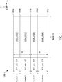
1 ist ein Schaubild eines Layout-Designs 100 gemäß einigen Ausführungsformen. Das Layout-Design 100 ist ein Layout-Schaubild eines integrierten Schaltkreises, wie zum Beispiel des integrierten Schaltkreises 300 der 3A-3B, des integrierten Schaltkreises 600 der 6A-6B, oder des integrierten Schaltkreises 800 der 8A-8B. In einigen Ausführungsformen ist mindestens ein Abschnitt des Layout-Designs 100 für die Herstellung des integrierten Schaltkreises 300 (3A-3B), des integrierten Schaltkreises 600 (6A-6B), oder des integrierten Schaltkreises 800 (8A-8B) verwendbar. 1 is a diagram of a layout design 100 according to some embodiments. The layout design 100 Figure 13 is a layout diagram of an integrated circuit, such as the integrated circuit 300 the 3A-3B , the integrated circuit 600 the 6A-6B , or the integrated circuit 800 the 8A-8B . In some embodiments, at least a portion of the layout is design 100 for the manufacture of the integrated circuit 300 ( 3A-3B) , the integrated circuit 600 ( 6A-6B) , or the integrated circuit 800 ( 8A-8B) usable.
Komponenten, die gleich oder ähnlich denen in jeder der 1, 2A-2B, 3A-3B, 4A-4B, 5A-5B, 6A-6B, 7A-7B, 8A-8B, 9A-9C, 10A-10E, 11, 12A-12B und 13-14 sind, erhalten die gleichen Bezugszahlen, und auf eine ähnliche detaillierte Beschreibung wird darum verzichtet.Components that are the same or similar to those in each of the 1 , 2A-2B , 3A-3B , 4A-4B , 5A-5B , 6A-6B , 7A-7B , 8A-8B , 9A-9C , 10A-10E , 11 , 12A-12B and 13-14 are given the same reference numerals and similar detailed descriptions are therefore omitted.
Das Layout-Design 100A umfasst die Layout-Designs 102a, 102b, 104a und 104b. In einigen Ausführungsformen umfasst das Layout-Design 100A zusätzliche Elemente, die in 1 nicht gezeigt sind.The layout design 100A includes the layout designs 102a , 102b , 104a and 104b . In some embodiments, the layout includes design 100A additional elements included in 1 are not shown.
In einigen Ausführungsformen entsprechen die Layout-Designs 102a und 104a mindestens dem Layout-Design 200 der 2A-2B, dem Layout-Design 500 der 5A-5B, oder dem Layout-Design 700 der 7A-7B. In einigen Ausführungsformen entsprechen die Layout-Designs 102b und 104b mindestens dem Layout-Design 200 der 2A-2B, dem Layout-Design 500 der 5A-5B, oder dem Layout-Design 700 der 7A-7B.In some embodiments, the layout designs are the same 102a and 104a at least the layout design 200 the 2A-2B , the layout design 500 the 5A-5B , or the layout design 700 the 7A-7B . In some embodiments, the layout designs are the same 102b and 104b at least the layout design 200 the 2A-2B , the layout design 500 the 5A-5B , or the layout design 700 the 7A-7B .
In einigen Ausführungsformen wird mindestens das Layout-Design 102a, 102b, 104a oder 104a als eine Zelle bezeichnet und ist standardzellenartig. In einigen Ausführungsformen umfasst „standardzellenartig“ eine Zelle, die keine Standardzelle ist, aber einige Ähnlichkeiten mit einer Standardzelle aufweist.In some embodiments, at least the layout design 102a , 102b , 104a or 104a referred to as a cell and is standard cellular. In some embodiments, “standard cell-like” includes a cell that is not a standard cell, but has some similarities to a standard cell.
Jedes der Layout-Designs 102a, 102b, 104a und 104b erstreckt sich in mindestens einer ersten Richtung X. Jedes der Layout-Designs 102a, 102b, 104a und 104b ist von einem anderen der Layout-Designs 102a, 102b, 104a und 104b in einer zweiten Richtung Y getrennt. Die zweite Richtung Y unterscheidet sich von der ersten Richtung X. In einigen Ausführungsformen ist die zweite Richtung Y die gleiche wie die erste Richtung X.Any of the layout designs 102a , 102b , 104a and 104b extends in at least a first direction X. Each of the layout designs 102a , 102b , 104a and 104b is from a different one of the layout designs 102a , 102b , 104a and 104b separated in a second direction Y. The second direction Y is different from the first direction X. In some embodiments, the second direction Y is the same as the first direction X.
Das Layout-Design 102a hat eine Zellengrenze 101a, die sich in einer ersten Richtung X erstreckt. In einigen Ausführungsformen grenzt das Layout-Design 102a in der ersten Richtung entlang der Zellengrenze 101a an andere Layout-Designs (zur besseren Übersichtlichkeit der Veranschaulichung nicht gezeigt).The layout design 102a has a cell boundary 101a which extends in a first direction X. In some embodiments, the layout design is delimited 102a in the first direction along the cell boundary 101a to other layout designs (not shown for clarity of illustration).
Das Layout-Design 102a grenzt in der ersten Richtung X entlang einer Zellengrenze 101b an das Layout-Design 104a. Das Layout-Design 104a grenzt in der ersten Richtung X entlang einer Zellengrenze 101c an das Layout-Design 102b. Das Layout-Design 102b grenzt in der ersten Richtung X entlang der Zellengrenze 101d an das Layout-Design 104b.The layout design 102a bounds in the first direction X along a cell boundary 101b to the layout design 104a . The layout design 104a bounds in the first direction X along a cell boundary 101c to the layout design 102b . The layout design 102b bounds in the first direction X along the cell boundary 101d to the layout design 104b .
Das Layout-Design 104b hat eine Zellengrenze 101e, die sich in der ersten Richtung X erstreckt. In einigen Ausführungsformen grenzt das Layout-Design 104b in der ersten Richtung entlang der Zellengrenze 101e an andere Layout-Designs an (zur besseren Übersichtlichkeit der Veranschaulichung nicht gezeigt).The layout design 104b has a cell boundary 101e extending in the first direction X. In some embodiments, the layout design is delimited 104b in the first direction along the cell boundary 101e to other layout designs (not shown for clarity of illustration).
Andere Konfigurationen oder Mengen von Layout-Designs 102a, 102b, 104a und 104b liegen ebenfalls innerhalb des Geltungsbereichs der vorliegenden Offenbarung. Zum Beispiel umfasst das Layout-Design 100 von 1 eine Spalte (Spalte 1) und vier Reihen (Reihen 1-4) von Zellen (zum Beispiel Layout-Designs 102a, 102b, 104a und 104b). Andere Anzahlen von Reihen und/oder Spalten in dem Layout-Design 100 liegen ebenfalls innerhalb des Geltungsbereichs der vorliegenden Offenbarung. Zum Beispiel umfasst das Layout-Design 100 in einigen Ausführungsformen mindestens eine zusätzliche Spalte von Zellen, die der Spalte 1 ähnelt und an die Spalte 1 grenzt. Zum Beispiel umfasst das Layout-Design 100 in einigen Ausführungsformen zusätzliche Reihen von Zellen, ähnlich den Reihen 3 und 4, die entlang der Zellengrenze 101a an die Reihe 1 grenzen. Zum Beispiel umfasst das Layout-Design 100 in einigen Ausführungsformen zusätzliche Reihen von Zellen, ähnlich den Reihen 1 und 2, die entlang der Zellengrenze 101e an die Reihe 4 grenzen. Zum Beispiel umfasst das Layout-Design 100 in einigen Ausführungsformen mindestens eine zusätzliche Reihe von Zellen, ähnlich der Reihe 3, neben der Reihe 4 entlang der entsprechenden Zellengrenze 101e. In einigen Ausführungsformen wechseln sich die Layout-Designs 102a und 104a mit den Layout-Designs 102b oder 104b in der zweiten Richtung Y ab.Other configurations or sets of layout designs 102a , 102b , 104a and 104b are also within the scope of the present disclosure. For example, the layout includes design 100 from 1 a column (column 1 ) and four rows (rows 1-4 ) of cells (for example layout designs 102a , 102b , 104a and 104b) . Other numbers of rows and / or columns in the layout design 100 are also within the scope of the present disclosure. For example, the layout includes design 100 in some embodiments, at least one additional column of cells that make up the column 1 resembles and attached to the column 1 borders. For example, the layout includes design 100 in some embodiments, additional rows of cells, similar to the rows 3 and 4th running along the cell boundary 101a your turn 1 limits. For example, the layout includes design 100 in some embodiments, additional rows of cells, similar to the rows 1 and 2 running along the cell boundary 101e your turn 4th limits. For example, the layout includes design 100 in some embodiments, at least one additional row of cells, similar to the row 3 , next to the row 4th along the corresponding cell boundary 101e . In some embodiments, the layout designs alternate 102a and 104a with the layout designs 102b or 104b in the second direction Y from.
Jedes der Layout-Designs 102a und 102b hat eine Höhe H1 in der zweiten Richtung Y. Die Layout-Designs 102a und 102b gleichen einander. In einigen Ausführungsformen unterscheiden sich die Layout-Designs 102a und 102b voneinander.Any of the layout designs 102a and 102b has a height H1 in the second direction Y. The layout designs 102a and 102b resemble each other. In some embodiments, the layout designs differ 102a and 102b from each other.
Jedes der Layout-Designs 104a und 104b hat eine Höhe H2 in der zweiten Richtung Y. Die Höhe H2 unterscheidet sich von der Höhe H1. Die Layout-Designs 104a und 104b gleichen einander. In einigen Ausführungsformen unterscheiden sich die Layout-Designs 104a und 104b voneinander.Any of the layout designs 104a and 104b has a height H2 in the second direction Y. The height H2 differs from the height H1 . The layout designs 104a and 104b resemble each other. In some embodiments, the layout designs differ 104a and 104b from each other.
In einigen Ausführungsformen haben die Layout-Designs 102a und 104a eine Höhe H3 in der zweiten Richtung Y, die gleich der Summe der Höhe H1 und der Höhe H2 ist. In einigen Ausführungsformen haben die Layout-Designs 102b und 104b eine Höhe H3 in der zweiten Richtung Y, die gleich der Summe der Höhe H1 und der Höhe H2 ist.In some embodiments, the layouts have designs 102a and 104a a height H3 in the second direction Y, which is equal to the sum of the height H1 and the height H2 is. In some embodiments, the layouts have designs 102b and 104b a height H3 in the second direction Y, which is equal to the sum of the height H1 and the height H2 is.
Mindestens das Layout-Design 102a oder 102b eignet sich zur Herstellung der Zelle 301 der 3A-3B, der Zelle 601 der 6A-6B und der Zelle 801 der 8A-8B. Mindestens das Layout-Design 104a oder 104b eignet sich zur Herstellung der Zelle 303 der 3A-3B, der Zelle 603 der 6A-6B und der Zelle 803 der 8A-8B.At least the layout design 102a or 102b is suitable for making the cell 301 the 3A-3B , the cell 601 the 6A-6B and the cell 801 the 8A-8B . At least the layout design 104a or 104b is suitable for making the cell 303 the 3A-3B , the cell 603 the 6A-6B and the cell 803 the 8A-8B .
In einigen Ausführungsformen sind eines oder mehrere der Layout-Designs 102a, 102b, 104a und 104b ein Layout-Design einer Logikgatterzelle. In einigen Ausführungsformen umfasst eine Logikgatterzelle eine AND-, OR-, NAND-, NOR-, XOR-, INV-, AND-OR-Invert-(AOI), OR-AND-Invert- (OAI), MUX-, Flip-Flop-, BUFF-, Latch-, Verzögerungs- oder Taktzelle. In einigen Ausführungsformen sind eines oder mehrere der Layout-Designs 102a, 102b, 104a und 104b ein Layout-Design einer Speicherzelle. In einigen Ausführungsformen umfasst eine Speicherzelle einen statischen Direktzugriffsspeicher (Static Random Access Memory, SRAM), einen dynamischen RAM (Dynamic RAM, DRAM), einen resistiven RAM (Resistive RAM, RRAM), einen magnetoresistiven RAM (Magnetoresistive RAM, MRAM) oder einen Nurlesespeicher (Read Only Memory, ROM). In einigen Ausführungsformen umfassen eines oder mehrere der Layout-Designs 102a, 102b, 104a und 1084b Layout-Designs eines oder mehrerer aktiver oder passiver Elemente. Zu nicht-einschränkenden Beispielen für aktive Elemente gehören Transistoren und Dioden. Zu nicht-einschränkenden Beispielen für Transistoren gehören Metall-Oxid-Halbleiter-Feldeffekttransistoren (MOSFET), komplementäre Metall-Oxid-Halbleiter-Transistoren (CMOS-Transistoren), Bipolartransistoren (Bipolar Junction Transistors, BJT), Hochspannungstransistoren, Hochfrequenztransistoren, p-Kanal- und/oder n-Kanal-Feldeffekttransistoren (PFETs/NFETs) usw.), FinFETs und planare MOS-Transistoren mit erhöhtem Source/Drain. Zu nicht-einschränkenden Beispielen für passive Elemente gehören Kondensatoren, Induktivitäten, Sicherungen und Widerstände.In some embodiments, one or more of the layout designs are 102a , 102b , 104a and 104b a layout design of a logic gate cell. In some embodiments, a logic gate cell comprises an AND, OR, NAND, NOR, XOR, INV, AND-OR-invert (AOI), OR-AND-invert (OAI), MUX, flip Flop, BUFF, latch, delay or clock cell. In some embodiments, one or more of the layout designs are 102a , 102b , 104a and 104b a layout design of a memory cell. In some embodiments, a memory cell includes static random access memory (SRAM), dynamic RAM (DRAM), resistive RAM (RRAM), magnetoresistive RAM (MRAM), or read-only memory (Read Only Memory, ROM). In some embodiments, include one or more of the layout designs 102a , 102b , 104a and 1084b Layout designs of one or more active or passive elements. To not- Limiting examples of active elements include transistors and diodes. Non-limiting examples of transistors include metal-oxide-semiconductor field effect transistors (MOSFET), complementary metal-oxide-semiconductor (CMOS) transistors, bipolar junction transistors (BJT), high voltage transistors, high frequency transistors, p-channel transistors and / or n-channel field effect transistors (PFETs / NFETs, etc.), FinFETs and planar MOS transistors with increased source / drain. Non-limiting examples of passive elements include capacitors, inductors, fuses, and resistors.
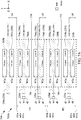
2A-2B sind Schaubilder eines Layout-Designs gemäß einigen Ausführungsformen. 2A-2B 13 are diagrams of a layout design in accordance with some embodiments.
2A-2B sind Schaubilder eines Layout-Designs 200 eines integrierten Schaltkreises 300 der 3A-3B gemäß einigen Ausführungsformen. 2A-2B are diagrams of a layout design 200 an integrated circuit 300 the 3A-3B according to some embodiments.
Das Layout-Design 200 ist eine Ausführungsform der Layout-Designs 102a und 104a von 1 oder der Layout-Designs 102b und 104b von 1.The layout design 200 is an embodiment of the layout designs 102a and 104a from 1 or the layout designs 102b and 104b from 1 .
Das Layout-Design 200 ist für die Herstellung des integrierten Schaltkreises 300 verwendbar.The layout design 200 is for the manufacture of the integrated circuit 300 usable.
Zur einfacheren Veranschaulichung sind einige der beschrifteten Elemente der 2A-2B, 3A-3B, 5A-5B, 6A-6B, 7A-7B oder 8A-8B mindestens in den 2A-2B, 3A-3B, 5A-5B, 6A-6B, 7A-7B oder 8A-8B nicht beschriftet. In einigen Ausführungsformen enthalten die 2A-2B, 3A-3B, 5A-5B, 6A-6B, 7A-7B oder 8A-8B zusätzliche Elemente, die nicht gezeigt sind.For ease of illustration, some of the labeled elements are the 2A-2B , 3A-3B , 5A-5B , 6A-6B , 7A-7B or 8A-8B at least in the 2A-2B , 3A-3B , 5A-5B , 6A-6B , 7A-7B or 8A-8B not labeled. In some embodiments, the 2A-2B , 3A-3B , 5A-5B , 6A-6B , 7A-7B or 8A-8B additional items not shown.
2A ist ein Schaubild eines Abschnitts 200A des Layout-Designs 200 der 2A-2B, das zur übersichtlicheren Veranschaulichung vereinfacht ist. Zum Beispiel zeigt im Vergleich zu 2B der Abschnitt 200A von 2A keinen Satz Layoutstrukturen 230 und 232 für leitende Merkmale von 2B, um die Darstellung übersichtlicher zu machen. 2A is a diagram of a section 200A of the layout design 200 the 2A-2B which is simplified for a clearer illustration. For example shows compared to 2 B the section 200A from 2A no set of layout structures 230 and 232 for conducting features of 2 B to make the presentation clearer.
Das Layout-Design 200 hat eine Höhe H3 in der zweiten Richtung Y. Das Layout-Design 200 umfasst ein Zellenlayout-Design 201 und ein Zellenlayout-Design 203. Das Zellenlayout-Design 201 hat eine Höhe H1 in der zweiten Richtung Y, und das Zellenlayout-Design 203 hat eine Höhe H2 in der zweiten Richtung Y.The layout design 200 has a height H3 in the second direction Y. The layout design 200 includes a cell layout design 201 and a cell layout design 203 . The cell layout design 201 has a height H1 in the second direction Y, and the cell layout design 203 has a height H2 in the second direction Y.
Das Zellenlayout-Design 201 ist eine Ausführungsform des Layout-Designs 102a oder 104a von 1. Das Zellenlayout-Design 203 ist eine Ausführungsform des Layout-Designs 102b oder 104b von 1. Das Zellenlayout-Design 201 oder 203 ist ein Layout-Design der entsprechenden Zelle 301 oder 303 (3A-3B) gemäß einigen Ausführungsformen. Das Zellenlayout-Design 201 oder 203 eignet sich zur Herstellung der entsprechenden Zelle 301 oder 303 (3A-3B) gemäß einigen Ausführungsformen.The cell layout design 201 is one embodiment of the layout design 102a or 104a from 1 . The cell layout design 203 is one embodiment of the layout design 102b or 104b from 1 . The cell layout design 201 or 203 is a layout design of the corresponding cell 301 or 303 ( 3A-3B) according to some embodiments. The cell layout design 201 or 203 is suitable for producing the corresponding cell 301 or 303 ( 3A-3B) according to some embodiments.
Das Layout-Design 200 umfasst des Weiteren Aktivregion-Layoutstrukturen 202a und 202b (gemeinsam als ein „Satz Aktivregion-Layoutstrukturen 202“ bezeichnet), die sich in der ersten Richtung X erstrecken. Die Aktivregion-Layoutstrukturen 202a und 202b des Satzes Aktivregion-Layoutstrukturen 202 sind in der zweiten Richtung Y voneinander getrennt. Die Aktivregion-Layoutstruktur 202a oder 202b kann zur Herstellung der entsprechenden aktiven Region 302a oder 302b eines Satzes aktiver Regionen 302 verwendet werden (3A-3B). In einigen Ausführungsformen wird der Satz Aktivregion-Layoutstrukturen 202 als eine Oxiddiffusionsregion (OD-Region) bezeichnet, die Source- oder Drain-Diffusionsregionen eines integrierten Schaltkreises 400B definiert (4B). In einigen Ausführungsformen eignet sich die Aktivregion-Layoutstruktur 202a oder 202b zur Herstellung einer aktiven Region 412 ( 4B) des integrierten Schaltkreises 400B.The layout design 200 also includes active region layout structures 202a and 202b (collectively referred to as a “set of active region layout structures 202”) extending in the first X direction. The active region layout structures 202a and 202b of the set of active region layout structures 202 are separated from each other in the second direction Y. The active region layout structure 202a or 202b can be used to produce the corresponding active region 302a or 302b a set of active regions 302 be used ( 3A-3B) . In some embodiments, the set becomes active region layout structures 202 referred to as an oxide diffusion region (OD region), the source or drain diffusion regions of an integrated circuit 400B Are defined ( 4B) . In some embodiments, the active region layout structure is suitable 202a or 202b to create an active region 412 ( 4B) of the integrated circuit 400B .
Das Layout-Design 200 umfasst des Weiteren Aktivregion-Layoutstrukturen 204a und 204b (gemeinsam als ein „Satz Aktivregion-Layoutstrukturen 204“ bezeichnet), die sich in der ersten Richtung X erstrecken. Die Aktivregion-Layoutstrukturen 204a und 204b des Satzes Aktivregion-Layoutstrukturen 204 sind in der zweiten Richtung Y voneinander getrennt. Die Aktivregion-Layoutstruktur 204a oder 204b kann zur Herstellung der entsprechenden aktiven Region 304a oder 304b eines Satzes aktiver Regionen 304 verwendet werden (3A-3B). In einigen Ausführungsformen definiert der Satz Aktivregion-Layoutstrukturen 204 Source- oder Drain-Diffusionsregionen des integrierten Schaltkreises 400B (4B). In einigen Ausführungsformen eignet sich die Aktivregion-Layoutstruktur 204a oder 204b zur Herstellung einer aktiven Region 412 (4B) des integrierten Schaltkreises 400B.The layout design 200 also includes active region layout structures 204a and 204b (collectively referred to as a “set of active region layout structures 204”) extending in the first X direction. The active region layout structures 204a and 204b of the set of active region layout structures 204 are separated from each other in the second direction Y. The active region layout structure 204a or 204b can be used to produce the corresponding active region 304a or 304b a set of active regions 304 be used ( 3A-3B) . In some embodiments, the set defines active region layout structures 204 Source or drain diffusion regions of the integrated circuit 400B ( 4B) . In some embodiments, the active region layout structure is suitable 204a or 204b to create an active region 412 ( 4B) of the integrated circuit 400B .
Das Layout-Design 200 umfasst des Weiteren Aktivregion-Layoutstrukturen 206a und 206b (gemeinsam als ein „Satz Aktivregion-Layoutstrukturen 206“ bezeichnet), die sich in der ersten Richtung X erstrecken. Die Aktivregion-Layoutstrukturen 206a und 206b des Satzes Aktivregion-Layoutstrukturen 206 sind in der zweiten Richtung Y voneinander getrennt. Die Aktivregion-Layoutstruktur 206a oder 206b kann zur Herstellung der entsprechenden aktiven Region 306a oder 306b eines Satzes aktiver Regionen 306 verwendet werden (3A-3B). In einigen Ausführungsformen definiert der Satz Aktivregion-Layoutstrukturen 206 Source- oder Drain-Diffusionsregionen eines integrierten Schaltkreises 400A (4A). In einigen Ausführungsformen eignet sich die Aktivregion-Layoutstruktur 206a oder 206b zur Herstellung einer aktiven Region 402 (4A) des integrierten Schaltkreises 400A.The layout design 200 also includes active region layout structures 206a and 206b (collectively referred to as a “set of active region layout structures 206”) extending in the first X direction. The active region layout structures 206a and 206b of the set of active region layout structures 206 are separated from each other in the second direction Y. The active region layout structure 206a or 206b can be used to produce the corresponding active region 306a or 306b a set of active regions 306 be used ( 3A-3B) . In some embodiments, the set defines active region layout structures 206 Source or drain diffusion regions of an integrated circuit 400A ( 4A) . In some embodiments, the Active region layout structure 206a or 206b to create an active region 402 ( 4A) of the integrated circuit 400A .
Das Layout-Design 200 umfasst des Weiteren Aktivregion-Layoutstrukturen 208a und 208b (gemeinsam als ein „Satz Aktivregion-Layoutstrukturen 208“ bezeichnet), die sich in der ersten Richtung X erstrecken. Die Aktivregion-Layoutstrukturen 208a und 208b des Satzes Aktivregion-Layoutstrukturen 208 sind in der zweiten Richtung Y voneinander getrennt. Die Aktivregion-Layoutstruktur 208a oder 208b kann zur Herstellung der entsprechenden aktiven Region 308a oder 308b eines Satzes aktiver Regionen 308 verwendet werden (3A-3B). In einigen Ausführungsformen definiert der Satz Aktivregion-Layoutstrukturen 208 Source- oder Drain-Diffusionsregionen des integrierten Schaltkreises 400B (4B). In einigen Ausführungsformen eignet sich die Aktivregion-Layoutstruktur 208a oder 208b zur Herstellung einer aktiven Region 412 (4B) des integrierten Schaltkreises 400B.The layout design 200 also includes active region layout structures 208a and 208b (collectively referred to as a “set of active region layout structures 208”) extending in the first X direction. The active region layout structures 208a and 208b of the set of active region layout structures 208 are separated from each other in the second direction Y. The active region layout structure 208a or 208b can be used to produce the corresponding active region 308a or 308b a set of active regions 308 be used ( 3A-3B) . In some embodiments, the set defines active region layout structures 208 Source or drain diffusion regions of the integrated circuit 400B ( 4B) . In some embodiments, the active region layout structure is suitable 208a or 208b to create an active region 412 ( 4B) of the integrated circuit 400B .
Das Layout-Design 200 umfasst des Weiteren Aktivregion-Layoutstrukturen 210a und 210b (gemeinsam als ein „Satz Aktivregion-Layoutstrukturen 210“ bezeichnet), die sich in der ersten Richtung X erstrecken. Die Aktivregion-Layoutstrukturen 210a und 210b des Satzes Aktivregion-Layoutstrukturen 210 sind in der zweiten Richtung Y voneinander getrennt. Die Aktivregion-Layoutstruktur 210a oder 210b kann zur Herstellung der entsprechenden aktiven Region 310a oder 310b eines Satzes aktiver Regionen 310 verwendet werden (3A-3B). In einigen Ausführungsformen definiert der Satz Aktivregion-Layoutstrukturen 210 Source- oder Drain-Diffusionsregionen eines integrierten Schaltkreises 400B (4B). In einigen Ausführungsformen eignet sich die Aktivregion-Layoutstruktur 210a oder 210b zur Herstellung einer aktiven Region 412 (4B) des integrierten Schaltkreises 400B.The layout design 200 also includes active region layout structures 210a and 210b (collectively referred to as a “set of active region layout structures 210”) extending in the first X direction. The active region layout structures 210a and 210b of the set of active region layout structures 210 are separated from each other in the second direction Y. The active region layout structure 210a or 210b can be used to produce the corresponding active region 310a or 310b a set of active regions 310 be used ( 3A-3B) . In some embodiments, the set defines active region layout structures 210 Source or drain diffusion regions of an integrated circuit 400B ( 4B) . In some embodiments, the active region layout structure is suitable 210a or 210b to create an active region 412 ( 4B) of the integrated circuit 400B .
In einigen Ausführungsformen sind die Aktivregion-Layoutstrukturen 202a, 204a, 204b und 206a Teil des Zellenlayout-Designs 201. In einigen Ausführungsformen sind die Aktivregion-Layoutstrukturen 206b, 208a, 208b und 210a Teil des Zellenlayout-Designs 203. In einigen Ausführungsformen ist die Aktivregion-Layoutstruktur 202b Teil eines Zellenlayout-Designs, das sich von dem Zellenlayout-Design 201 oder 203 unterscheidet. In einigen Ausführungsformen ist die Aktivregion-Layoutstruktur 210b Teil eines anderen Zellenlayout-Designs, das sich von dem Zellenlayout-Design 201 oder 203 unterscheidet.In some embodiments, the active region are layout structures 202a , 204a , 204b and 206a Part of the cell layout design 201 . In some embodiments, the active region are layout structures 206b , 208a , 208b and 210a Part of the cell layout design 203 . In some embodiments, the active region is layout structure 202b Part of a cell layout design that differs from the cell layout design 201 or 203 differs. In some embodiments, the active region is layout structure 210b Part of a different cell layout design that is different from the cell layout design 201 or 203 differs.
In einigen Ausführungsformen entspricht der Satz Aktivregion-Layoutstrukturen 202, 206 und 210 dem Satz aktiver Regionen 302, 306 und 310 eines ersten Vorrichtungstyps, und der Satz Aktivregion-Layoutstrukturen 204 und 208 entspricht dem Satz aktiver Regionen 304 bzw. 308 eines zweiten Vorrichtungstyps, der sich von dem ersten Vorrichtungstyp unterscheidet.In some embodiments, the set corresponds to active region layout structures 202 , 206 and 210 the set of active regions 302 , 306 and 310 of a first type of device, and the set of active region layout structures 204 and 208 corresponds to the set of active regions 304 respectively. 308 a second type of device different from the first type of device.
In einigen Ausführungsformen ist der erste Vorrichtungstyp ein n-FinFET, und der zweite Vorrichtungstyp ist ein p-FinFET. In einigen Ausführungsformen entsprechen zum Beispiel Aktivregion-Layoutstrukturen 202a, 202b, 206a, 206b, 210a und 210b aktiven Regionen 302a, 302b, 306a, 306b, 310a und 310b von n-FinFET-Transistoren, und Aktivregion-Layoutstrukturen 204a, 204b, 208a und 208b entsprechen aktiven Regionen 304a, 304b, 308a und 308b von p-FinFET-Transistoren. In einigen Ausführungsformen kann mindestens die Aktivregion-Layoutstruktur 202a, 202b, 206a, 206b, 210a und 210b verwendet werden, um entsprechende aktive Regionen 302a, 302b, 306a, 306b, 310a und 310b (zum Beispiel Source- und Drain-Regionen von n-FinFET-Transistoren) herzustellen, und mindestens die Aktivregion-Layoutstruktur 204a, 204b, 208a und 208b kann verwendet werden, um entsprechende aktive Regionen 304a, 304b, 308a und 308b (zum Beispiel Source- und Drain-Regionen von p-FinFET-Transistoren) herzustellen.In some embodiments, the first type of device is an n-FinFET and the second type of device is a p-FinFET. For example, in some embodiments, active region layout structures correspond 202a , 202b , 206a , 206b , 210a and 210b active regions 302a , 302b , 306a , 306b , 310a and 310b of n-FinFET transistors, and active region layout structures 204a , 204b , 208a and 208b correspond to active regions 304a , 304b , 308a and 308b of p-FinFET transistors. In some embodiments, at least the active region layout structure may be 202a , 202b , 206a , 206b , 210a and 210b used to corresponding active regions 302a , 302b , 306a , 306b , 310a and 310b (e.g. source and drain regions of n-FinFET transistors), and at least the active region layout structure 204a , 204b , 208a and 208b can be used to identify corresponding active regions 304a , 304b , 308a and 308b (e.g. source and drain regions of p-FinFET transistors).
In einigen Ausführungsformen ist der erste Vorrichtungstyp ein p-Typ FinFET, und der zweite Vorrichtungstyp ist ein n-Typ FinFET. In einigen Ausführungsformen entsprechen zum Beispiel Aktivregion-Layoutstrukturen 202a, 202b, 206a, 206b, 210a und 210b aktiven Regionen 302a, 302b, 306a, 306b, 310a und 310b von p-FinFET-Transistoren, und Aktivregion-Layoutstrukturen 204a, 204b, 208a und 208b entsprechen aktiven Regionen 304a, 304b, 308a und 308b von n-FinFET-Transistoren. In einigen Ausführungsformen kann mindestens die Aktivregion-Layoutstruktur 202a, 202b, 206a, 206b, 210a und 210b verwendet werden, um entsprechende aktive Regionen 302a, 302b, 306a, 306b, 310a und 310b (zum Beispiel Source- und Drain-Regionen von p-FinFET-Transistoren) herzustellen, und mindestens die Aktivregion-Layoutstruktur 204a, 204b, 208a und 208b kann verwendet werden, um die entsprechenden aktiven Regionen 304a, 304b, 308a und 308b (zum Beispiel Source- und Drain-Regionen von n-FinFET-Transistoren) herzustellen. In einigen Ausführungsformen liegt ein anderer Transistortyp für mindestens den Satz Aktivregion-Layoutstrukturen 202, 204, 206, 208 oder 210 oder den Satz aktiver Regionen 302, 304, 306, 308 oder 310 innerhalb des Geltungsbereichs der vorliegenden Offenbarung.In some embodiments, the first type of device is a p-type FinFET and the second type of device is an n-type FinFET. For example, in some embodiments, active region layout structures correspond 202a , 202b , 206a , 206b , 210a and 210b active regions 302a , 302b , 306a , 306b , 310a and 310b of p-FinFET transistors, and active region layout structures 204a , 204b , 208a and 208b correspond to active regions 304a , 304b , 308a and 308b of n-FinFET transistors. In some embodiments, at least the active region layout structure may be 202a , 202b , 206a , 206b , 210a and 210b used to corresponding active regions 302a , 302b , 306a , 306b , 310a and 310b (e.g. source and drain regions of p-FinFET transistors), and at least the active region layout structure 204a , 204b , 208a and 208b can be used to identify the corresponding active regions 304a , 304b , 308a and 308b (e.g. source and drain regions of n-FinFET transistors). In some embodiments, a different type of transistor resides for at least the set of active region layout structures 202 , 204 , 206 , 208 or 210 or the set of active regions 302 , 304 , 306 , 308 or 310 within the scope of the present disclosure.
In einigen Ausführungsformen eignet sich mindestens die Aktivregion-Layoutstruktur 202a, 202b, 204a, 204b, 208a, 208b, 210a oder 210b zum Herstellen der Finnen 412a1, 412a2 und 412a3 der aktiven Region 412 (4B). In einigen Ausführungsformen kann mindestens die Aktivregion-Layoutstruktur 206a oder 206b verwendet werden, um die Finnen 402a1 und 402a2 der aktiven Region 402 herzustellen (4A).In some embodiments, at least the active region layout structure is suitable 202a , 202b , 204a , 204b , 208a , 208b , 210a or 210b for making the fins 412a1 , 412a2 and 412a3 the active region 412 ( 4B) . In some embodiments, at least the active region layout structure may be 206a or 206b used to Finns 402a1 and 402a2 the active region 402 to manufacture ( 4A) .
Obgleich der Satz Aktivregion-Layoutstrukturen 202, 204, 206, 208 und 210 der 2A-2B als zur Herstellung von Finnen aktiver Regionen 402 und 412 der 4A-4B geeignet beschrieben wird, versteht es sich, dass die Finnen der aktiven Region 402 oder 412 durch entsprechende Nanolagen oder Nanodrähte ersetzt werden können. Zum Beispiel ist in einigen Ausführungsformen mindestens die Aktivregion-Layoutstruktur 202a, 202b, 204a, 204b, 208a, 208b, 210a oder 210b geeignet, um Nanolagen (nicht gezeigt) für die aktive Region 412 eines Nanolagen-Transistors herzustellen. Zum Beispiel ist in einigen Ausführungsformen mindestens die Aktivregion-Layoutstruktur 206a oder 206b geeignet, um Nanolagen (nicht gezeigt) für die aktive Region 402 eines Nanolagen-Transistors herzustellen. Zum Beispiel ist in einigen Ausführungsformen mindestens die Aktivregion-Layoutstruktur 202a, 202b, 204a, 204b, 208a, 208b, 210a oder 210b für die Herstellung von Nanodrähten (nicht gezeigt) für die aktive Region 412 eines Nanodrahttransistors geeignet. Zum Beispiel ist in einigen Ausführungsformen mindestens die Aktivregion-Layoutstruktur 206a oder 206b geeignet, um einen Nanodraht (nicht gezeigt) für die aktive Region 402 eines Nanodrahttransistors herzustellen.Although the set of active region layout structures 202 , 204 , 206 , 208 and 210 the 2A-2B than to produce fins of active regions 402 and 412 the 4A-4B is suitably described, it is to be understood that the Finns are the active region 402 or 412 can be replaced by appropriate nano layers or nanowires. For example, in some embodiments, at least the active region is layout structure 202a , 202b , 204a , 204b , 208a , 208b , 210a or 210b suitable to nanolayers (not shown) for the active region 412 of a nano-layer transistor. For example, in some embodiments, at least the active region is layout structure 206a or 206b suitable to nanolayers (not shown) for the active region 402 of a nano-layer transistor. For example, in some embodiments, at least the active region is layout structure 202a , 202b , 204a , 204b , 208a , 208b , 210a or 210b for making nanowires (not shown) for the active region 412 of a nanowire transistor. For example, in some embodiments, at least the active region is layout structure 206a or 206b suitable to make a nanowire (not shown) for the active region 402 of a nanowire transistor.
Die Aktivregion-Layoutstrukturen 202a, 202b, 204a, 204b, 208a, 208b, 210a und 210b haben jeweils eine Breite W2a in der zweiten Richtung Y. In einigen Ausführungsformen unterscheidet sich die Breite W2a von mindestens einer der Aktivregion-Layoutstrukturen 202a, 202b, 204a, 204b, 208a, 208b, 210a oder 210b von der Breite W2b von mindestens einer anderen der Aktivregion-Layoutstrukturen 202a, 202b, 204a, 204b, 208a, 208b, 210a oder 210b.The active region layout structures 202a , 202b , 204a , 204b , 208a , 208b , 210a and 210b each have a width W2a in the second direction Y. In some embodiments, the width W2a differs from at least one of the active region layout structures 202a , 202b , 204a , 204b , 208a , 208b , 210a or 210b the width W2b of at least one other of the active region layout structures 202a , 202b , 204a , 204b , 208a , 208b , 210a or 210b .
Die Aktivregion-Layoutstrukturen 206a und 206b haben jeweils eine Breite W2b in der zweiten Richtung Y. In einigen Ausführungsformen sind die Breiten W2b der Aktivregion-Layoutstrukturen 206a und 206b voneinander verschieden.The active region layout structures 206a and 206b each have a width W2b in the second direction Y. In some embodiments, the widths W2b are the active region layout structures 206a and 206b different from each other.
Die Breite W2a ist größer als die Breite W2b. In einigen Ausführungsformen steht mindestens die Breite W2a der Aktivregion-Layoutstrukturen 202a, 202b, 204a, 204b, 208a, 208b, 210a und 210b in direktem Zusammenhang mit der Anzahl der Finnen-Layoutstrukturen (nicht gezeigt), die zur Herstellung entsprechender Finnen in der aktiven Region 412 verwendet werden können. In einigen Ausführungsformen steht die Breite W2a der Aktivregion-Layoutstrukturen 202a, 202b, 204a, 204b, 208a, 208b, 210a und 210b im Zusammenhang mit der Anzahl leitender Vorrichtungen (zum Beispiel Transistoren), die durch den Satz Aktivregion-Layoutstrukturen 202, 204, 208 und 210 hergestellt werden, und der entsprechenden Geschwindigkeit und Ansteuerungsstärke der leitenden Vorrichtungen (zum Beispiel Transistoren) in den aktiven Regionen 302, 304, 308 und 310.The width W2a is larger than the width W2b. In some embodiments, at least the width W2a of the active region layout structures is 202a , 202b , 204a , 204b , 208a , 208b , 210a and 210b directly related to the number of fin layout structures (not shown) used to manufacture corresponding fins in the active region 412 can be used. In some embodiments, the width W2a of the active region layout structures is 202a , 202b , 204a , 204b , 208a , 208b , 210a and 210b related to the number of conductive devices (e.g., transistors) represented by the set of active region layout structures 202 , 204 , 208 and 210 and the corresponding speed and drive strength of the conductive devices (e.g. transistors) in the active regions 302 , 304 , 308 and 310 .
In einigen Ausführungsformen steht mindestens die Breite W2b der Aktivregion-Layoutstrukturen 206a und 206b in direktem Zusammenhang mit der Anzahl der Finnen-Layoutstrukturen (nicht gezeigt), die zur Herstellung entsprechender Finnen in der aktiven Region 402 verwendet werden können. In einigen Ausführungsformen steht die Breite W2b der Aktivregion-Layoutstrukturen 206a und 206b im Zusammenhang mit der Anzahl leitender Vorrichtungen (zum Beispiel Transistoren), die durch den Satz Aktivregion-Layoutstrukturen und 206 hergestellt werden, und der entsprechenden Geschwindigkeit und Ansteuerungsstärke der leitenden Vorrichtungen (zum Beispiel Transistoren) in den aktiven Regionen 306.In some embodiments, at least the width W2b of the active region layout structures is 206a and 206b directly related to the number of fin layout structures (not shown) used to manufacture corresponding fins in the active region 402 can be used. In some embodiments, the width W2b of the active region layout structures is 206a and 206b related to the number of conductive devices (e.g., transistors) fabricated by the set of active region layout structures 16 and 206 and the corresponding speed and drive strength of the conductive devices (e.g., transistors) in the active regions 306 .
In einigen Ausführungsformen führt zum Beispiel eine Vergrößerung der Breite W2a der Aktivregion-Layoutstrukturen 202a, 202b, 204a, 204b, 208a, 208b, 210a und 210b oder der Breite W2a der Aktivregion-Layoutstrukturen 206a und 206b dazu, dass die Anzahl der Finnen und die Anzahl der leitenden Vorrichtungen (zum Beispiel Transistoren), die durch einen Satz Aktivregion-Layoutstrukturen 202, 204, 206, 208 und 210 hergestellt werden, zunimmt, und die entsprechende Geschwindigkeit und Ansteuerungsstärke der leitenden Vorrichtungen (zum Beispiel Transistoren) steigt.In some embodiments, for example, increasing the width W2a of the active region layout structures results 202a , 202b , 204a , 204b , 208a , 208b , 210a and 210b or the width W2a of the active region layout structures 206a and 206b that the number of fins and the number of conductive devices (e.g., transistors) represented by a set of active region layout structures 202 , 204 , 206 , 208 and 210 is increased, and the corresponding speed and drive strength of the conductive devices (e.g. transistors) increases.
In einigen Ausführungsformen führt zum Beispiel eine Verringerung der Breite W2a der Aktivregion-Layoutstrukturen 202a, 202b, 204a, 204b, 208a, 208b, 210a und 210b oder der Breite W2a der Aktivregion-Layoutstrukturen 206a und 206b dazu, dass die Anzahl der Finnen und die Anzahl der leitenden Vorrichtungen (zum Beispiel Transistoren), die durch den Satz Aktivregion-Layoutstrukturen 202, 204, 206, 208 und 210 hergestellt werden, abnimmt, und die entsprechende Geschwindigkeit und Ansteuerungsstärke der leitenden Vorrichtungen (zum Beispiel Transistoren) nimmt ab.In some embodiments, for example, reducing the width W2a of the active region layout structures results 202a , 202b , 204a , 204b , 208a , 208b , 210a and 210b or the width W2a of the active region layout structures 206a and 206b that the number of fins and the number of conductive devices (e.g., transistors) represented by the set of active region layout structures 202 , 204 , 206 , 208 and 210 decreases, and the corresponding speed and drive strength of the conductive devices (e.g., transistors) decrease.
Da die Breite W2a größer ist als die Breite W2b, entsteht in einigen Ausführungsformen eine asymmetrische aktive Region innerhalb des Zellenlayout-Designs 201 oder 203. Zum Beispiel sind innerhalb des Zellenlayout-Designs 201 oder 203 die Breite W2a der Aktivregion-Layoutstrukturen in dem Satz Aktivregion-Layoutstrukturen 202, 204, 208 und 210 und die Breite W2b der Aktivregion-Layoutstrukturen in dem Satz Aktivregion-Layoutstrukturen 206 unterschiedlich, was zu einer asymmetrischen oder mit gemischten Breiten versehenen aktiven Region und entsprechenden Aktivregion-Layoutstrukturen führt.Because the width W2a is greater than the width W2b, an asymmetrical active region is created within the cell layout design in some embodiments 201 or 203 . For example, within the cell layout design 201 or 203 the width W2a of the active region layout structures in the set of active region layout structures 202 , 204 , 208 and 210 and the width W2b of the active region layout structures in the set of active region layout structures 206 different, resulting in an asymmetrical or mixed width active region and corresponding active region layout structures.
In einigen Ausführungsformen ist mindestens eine der Aktivregion-Layoutstrukturen in dem Satz Aktivregion-Layoutstrukturen 202, 204, 208 oder 210 geeignet, um einen entsprechenden Satz aktiver Regionen 302, 304, 308 oder 310 mit m Finnen herzustellen, und mindestens eine der Aktivregion-Layoutstrukturen in dem Satz Aktivregion-Layoutstrukturen 206 kann verwendet werden, um einen entsprechenden Satz aktiver Regionen 306 mit n Finnen herzustellen, wobei m eine ganze Zahl ist und n eine andere ganze Zahl ist. In einigen Ausführungsformen ist die ganze Zahl m nicht gleich der ganzen Zahl n, was dazu führt, dass das Zellenlayout-Design 201 oder 203 asymmetrische Aktivregion-Layoutstrukturen aufweist oder die Zelle 301 oder 303 asymmetrische aktive Regionen aufweist.In some embodiments, at least one of the active region layout structures in the set is active region layout structures 202 , 204 , 208 or 210 suitable to a corresponding set of active regions 302 , 304 , 308 or 310 with m fins, and at least one of the active region layout structures in the set of active region layout structures 206 can be used to set an appropriate set of active regions 306 with n fins, where m is an integer and n is another integer. In some embodiments, the integer m does not equal the integer n, which results in the cell layout design 201 or 203 Has asymmetrical active region layout structures or the cell 301 or 303 has asymmetric active regions.
In einigen Ausführungsformen ist zum Beispiel in dem Layout-Design 200 oder dem integrierten Schaltkreis 300 die ganze Zahl m gleich 3, und die ganze Zahl n ist gleich 2, so dass der Satz Aktivregion-Layoutstrukturen 202, 204, 208 und 210 zur Herstellung eines entsprechenden Satzes aktiver Regionen 302, 304, 308 und 310 mit 3 Finnen verwendet werden kann und der Satz Aktivregion-Layoutstrukturen 206 zur Herstellung eines entsprechenden Satzes aktiver Regionen 306 mit 2 Finnen verwendet werden kann. Andere Werte für mindestens die ganze Zahl m oder die ganze Zahl n liegen ebenfalls innerhalb des Geltungsbereichs der vorliegenden Offenbarung.For example, in some embodiments it is in the layout design 200 or the integrated circuit 300 the integer m is 3, and the integer n is 2, so the set of active region layout structures 202 , 204 , 208 and 210 to create a corresponding set of active regions 302 , 304 , 308 and 310 with 3 fins can be used and the set of active region layout structures 206 to create a corresponding set of active regions 306 can be used with 2 fins. Other values for at least the integer m or the integer n are also within the scope of the present disclosure.
In einigen Ausführungsformen unterscheidet sich in dem Zellenlayout-Design 201 oder 203 eine Summe der Breiten des Satzes Aktivregion-Layoutstrukturen 202, 204, 206, 208 und 210 des ersten Vorrichtungstyps von einer Summe der Breiten des Satzes Aktivregion-Layoutstrukturen 202, 204, 206, 208 und 210 des zweiten Vorrichtungstyps, was dazu führt, dass der erste Vorrichtungstyp und der zweite Vorrichtungstyp asymmetrische Aktivregion-Layoutstrukturen innerhalb des Zellenlayout-Designs 201 oder 203 oder asymmetrische aktive Regionen innerhalb der Zelle 301 und 303 aufweisen.In some embodiments, the cell layout design differs 201 or 203 a sum of the widths of the set of active region layout structures 202 , 204 , 206 , 208 and 210 of the first device type from a sum of the widths of the set of active region layout structures 202 , 204 , 206 , 208 and 210 of the second type of device, resulting in the first type of device and the second type of device having asymmetrical active region layout structures within the cell layout design 201 or 203 or asymmetric active regions within the cell 301 and 303 exhibit.
In einigen Ausführungsformen ist zum Beispiel der erste Vorrichtungstyp ein n-FinFET, und der zweite Vorrichtungstyp ist ein p-FinFET, und die Summe der Breiten der Aktivregion-Layoutstrukturen 202a und 206a (die gleich einer Summe von W2a und W2b ist) ist kleiner als die Summe der Breiten der Aktivregion-Layoutstrukturen 204a und 204b (die gleich 2*W2a ist), und somit ist für das Zellenlayout-Design 201 die Stärke der n-FinFETs kleiner als die Stärke der p-FinFETs. In diesen Ausführungsformen ist für das Zellenlayout-Design 203 die Stärke der n-FinFETs aus ähnlichen Gründen wie bei dem Zellenlayout-Design 201 geringer als die Stärke der p-FinFETs, weshalb im Interesse der Kürze nicht mehr darauf eingegangen wird.For example, in some embodiments, the first device type is an n-FinFET and the second device type is a p-FinFET, and the sum of the widths of the active region layout structures 202a and 206a (which is equal to a sum of W2a and W2b) is smaller than the sum of the widths of the active region layout structures 204a and 204b (which is equal to 2 * W2a), and thus is for the cell layout design 201 the strength of the n-FinFETs is smaller than the strength of the p-FinFETs. In these embodiments is for the cell layout design 203 the strength of the n-type FinFETs for reasons similar to the cell layout design 201 less than the strength of the p-FinFETs, which is why in the interest of brevity it will not be discussed again.
In einigen Ausführungsformen ist zum Beispiel der erste Vorrichtungstyp ein p-FinFET, und der zweite Vorrichtungstyp ist ein n-FinFET, und die Summe der Breiten der Aktivregion-Layoutstrukturen 202a und 206a (die gleich einer Summe von W2a und W2b ist) ist kleiner als die Summe der Breiten der Aktivregion-Layoutstrukturen 204a und 204b (die gleich 2*W2a ist), und somit ist für das Zellenlayout-Design 201 die Stärke der p-FinFETs kleiner als die Stärke der n-FinFETs. In diesen Ausführungsformen ist für das Zellenlayout-Design 203 die Stärke der p-FinFETs aus ähnlichen Gründen wie bei dem Zellenlayout-Design 201 geringer als die Stärke der n-FinFETs, weshalb im Interesse der Kürze nicht mehr darauf eingegangen wird.For example, in some embodiments, the first device type is a p-FinFET and the second device type is an n-FinFET, and the sum of the widths of the active region layout structures 202a and 206a (which is equal to a sum of W2a and W2b) is smaller than the sum of the widths of the active region layout structures 204a and 204b (which is equal to 2 * W2a), and thus is for the cell layout design 201 the strength of the p-FinFETs is smaller than the strength of the n-FinFETs. In these embodiments is for the cell layout design 203 the strength of the p-FinFETs for reasons similar to the cell layout design 201 lower than the strength of the n-FinFETs, which is why it will not be discussed further in the interests of brevity.
In einigen Ausführungsformen unterscheidet sich in dem Zellenlayout-Design 201 oder 203 die Summe einer Anzahl von Finnen, die durch den Satz Aktivregion-Layoutstrukturen 202, 204, 206, 208 oder 210 des ersten Vorrichtungstyps hergestellt werden, von einer Summe einer Anzahl von Finnen, die durch den Satz Aktivregion-Layoutstrukturen 202, 204, 206, 208 oder 210 des zweiten Vorrichtungstyps hergestellt werden, was dazu führt, dass der erste Vorrichtungstyp und der zweite Vorrichtungstyp asymmetrische Aktivregion-Layoutstrukturen innerhalb des Zellenlayout-Designs 201 oder 203 oder asymmetrische aktive Regionen innerhalb der Zelle 301 und 303 aufweisen.In some embodiments, the cell layout design differs 201 or 203 the sum of a number of fins defined by the set of active region layout structures 202 , 204 , 206 , 208 or 210 of the first type of device can be made from a sum of a number of fins defined by the set of active region layout structures 202 , 204 , 206 , 208 or 210 of the second type of device, resulting in the first type of device and the second type of device having asymmetrical active region layout structures within the cell layout design 201 or 203 or asymmetric active regions within the cell 301 and 303 exhibit.
In einigen Ausführungsformen ist zum Beispiel der erste Vorrichtungstyp ein n-FinFET, und der zweite Vorrichtungstyp ist ein p-FinFET, und die Summe der Finnen der Aktivregion-Layoutstrukturen 202a und 206a oder der aktiven Regionen 302a und 306a (die gleich 5 ist (zum Beispiel eine Summe aus 3 und 2)) ist kleiner als die Summe der Finnen der Aktivregion-Layoutstrukturen 204a und 204b oder aktiven Regionen 304a und 304b (die gleich 6 ist (zum Beispiel eine Summe aus 3 und 3)), und somit ist für das Zellenlayout-Design 201 die Stärke der n-FinFETs geringer als die Stärke der p-FinFETs. In diesen Ausführungsformen ist für das Zellenlayout-Design 203 die Stärke der n-FinFETs aus ähnlichen Gründen wie bei dem Zellenlayout-Design 201 geringer als die Stärke der p-FinFETs, weshalb im Interesse der Kürze nicht mehr darauf eingegangen wird.For example, in some embodiments, the first device type is an n-FinFET and the second device type is a p-FinFET, and the sum of the fins of the active region layout structures 202a and 206a or the active regions 302a and 306a (which is equal to 5 (for example, a sum of 3 and 2)) is smaller than the sum of the fins of the active region layout structures 204a and 204b or active regions 304a and 304b (which is equal to 6 (e.g. a sum of 3 and 3)), and thus is for the cell layout design 201 the strength of the n-FinFETs is less than the strength of the p-FinFETs. In these embodiments is for the cell layout design 203 the strength of the n-type FinFETs for reasons similar to the cell layout design 201 less than the strength of the p-FinFETs, which is why in the interest of brevity it will not be discussed again.
Wenn in diesen Ausführungsformen der erste Vorrichtungstyp ein n-FinFET ist und der zweite Vorrichtungstyp ein p-FinFET ist, dann ist eine Anzahl von n-FinFETs, die durch den Satz Aktivregion-Layoutstrukturen 202, 206 und 210 hergestellt werden, nicht größer als eine Anzahl von p-FinFETs, die durch den Satz Aktivregion-Layoutstrukturen 204 und 208 hergestellt werden.In these embodiments, if the first device type is an n-FinFET and the second device type is a p-FinFET, then a number of n-FinFETs are defined by the set of active region layout structures 202 , 206 and 210 can be fabricated no greater than a number of p-FinFETs defined by the set of active region layout structures 204 and 208 getting produced.
In einigen Ausführungsformen ist zum Beispiel der erste Vorrichtungstyp ein p-FinFET, und der zweite Vorrichtungstyp ist ein n-FinFET, und die Summe der Finnen der Aktivregion-Layoutstrukturen 202a und 206a oder der aktiven Regionen 302a und 306a (die gleich 5 ist (zum Beispiel eine Summe aus 3 und 2)) ist kleiner als die Summe der Finnen der Aktivregion-Layoutstrukturen 204a und 204b oder aktiven Regionen 304a und 304b (die gleich 6 ist (zum Beispiel eine Summe aus 3 und 3)), und somit ist für das Zellenlayout-Design 201 die Stärke der n-FinFETs geringer als die Stärke der p-FinFETs. In diesen Ausführungsformen ist für das Zellenlayout-Design 203 die Stärke der p-FinFETs aus ähnlichen Gründen wie bei dem Zellenlayout-Design 201 geringer als die Stärke der n-FinFETs, weshalb im Interesse der Kürze nicht mehr darauf eingegangen wird.For example, in some embodiments, the first type of device is a p-FinFET, and the second type of device is an n-FinFET, and the sum of the fins of the active region layout structures 202a and 206a or the active regions 302a and 306a (which is equal to 5 (for example, a sum of 3 and 2)) is smaller than the sum of the fins of the active region layout structures 204a and 204b or active regions 304a and 304b (which is equal to 6 (e.g. a sum of 3 and 3)), and thus is for the cell layout design 201 the strength of the n-FinFETs is less than the strength of the p-FinFETs. In these embodiments is for the cell layout design 203 the strength of the p-FinFETs for reasons similar to the cell layout design 201 lower than the strength of the n-FinFETs, which is why it will not be discussed further in the interests of brevity.
Wenn in diesen Ausführungsformen der erste Vorrichtungstyp ein p-FinFET ist und der zweite Vorrichtungstyp ein n-FinFET ist, dann ist eine Anzahl von p-FinFETs, die durch den Satz Aktivregion-Layoutstrukturen 202, 206 und 210 hergestellt werden, nicht größer als eine Anzahl von n-FinFETs, die durch den Satz Aktivregion-Layoutstrukturen 204 und 208 hergestellt werden.In these embodiments, if the first device type is a p-FinFET and the second device type is an n-FinFET, then a number of p-FinFETs are defined by the set of active region layout structures 202 , 206 and 210 can be fabricated no greater than a number of n-FinFETs defined by the set of active region layout structures 204 and 208 getting produced.
Daher können asymmetrische Aktivregion-Layoutstrukturen und entsprechende asymmetrische aktive Regionen zu einer möglichen nicht-ausbalancierten Vorrichtungsstärke zwischen den n-FinFET-Vorrichtungen und den p-FinFET-Vorrichtungen führen. Durch die Verwendung der Merkmale des Layout-Designs 200 werden jedoch die Breiten W2a und W2b oder die Anzahl von Finnen (zum Beispiel ganzzahliges m oder ganzzahliges n) so ausgewählt oder justiert, dass die Stärken der n-FinFET- und der p-FinFET-Vorrichtungen im Vergleich zu anderen Herangehensweisen besser ausbalanciert werden, was zu einer besseren Schaltkreisleistung führt als bei anderen Herangehensweisen.Therefore, asymmetrical active region layout structures and corresponding asymmetrical active regions can result in possible unbalanced device strength between the n-FinFET devices and the p-FinFET devices. By using the features of the layout design 200 however, the widths W2a and W2b or the number of fins (e.g., integer m or integer n) are selected or adjusted to better balance the strengths of the n-FinFET and p-FinFET devices compared to other approaches, resulting in better circuit performance than other approaches.
In einigen Ausführungsformen werden zum Beispiel die Positionen der n- oder p-FinFET-Vorrichtungen (zum Beispiel die Aktivregion-Layoutstrukturen 202a, 206a, 206b und 210a) an den Zellengrenzen (zum Beispiel der Zellengrenze 101a, 101b, 101c, 101d oder 101e) positioniert, um eine etwaige Fehlanpassung zwischen der Anzahl von Breiten W2a und W2b oder der Anzahl von Finnen in dem Layout-Design 200 im Vergleich zu anderen Herangehensweisen besser auszubalancieren.For example, in some embodiments, the locations of the n- or p-FinFET devices (e.g., the active region layout structures 202a , 206a , 206b and 210a) at the cell boundaries (for example the cell boundary 101a , 101b , 101c , 101d or 101e) positioned to avoid any mismatch between the number of widths W2a and W2b or the number of fins in the layout design 200 better balanced compared to other approaches.
In einigen Ausführungsformen ist der erste Vorrichtungstyp ein n-FinFET, und der zweite Vorrichtungstyp ist ein p-FinFET, und die Position der n-FinFETs (zum Beispiel die Aktivregion-Layoutstrukturen 202a, 206a, 206b und 210a) werden an Zellengrenzen (zum Beispiel der Zellengrenze 101a, 101b, 101c, 101d oder 101e) positioniert, um die Fehlanpassung zwischen der Anzahl von Breiten W2a und W2b oder der Anzahl von Finnen in dem Layout-Design 200 im Vergleich zu anderen Herangehensweisen besser auszubalancieren.In some embodiments, the first type of device is an n-FinFET and the second type of device is a p-FinFET, and the location of the n-FinFETs (e.g., the active region layout structures 202a , 206a , 206b and 210a) are at cell boundaries (for example the cell boundary 101a , 101b , 101c , 101d or 101e) positioned to address the mismatch between the number of widths W2a and W2b or the number of fins in the layout design 200 better balanced compared to other approaches.
In einigen Ausführungsformen ist der erste Vorrichtungstyp ein p-FinFET, und der zweite Vorrichtungstyp ist ein n-FinFET, und die Position der p-FinFETs (zum Beispiel die Aktivregion-Layoutstrukturen 202a, 206a, 206b und 210a) werden an Zellengrenzen (zum Beispiel der Zellengrenze 101a, 101b, 101c, 101d oder 101e) positioniert, um die Fehlanpassung zwischen der Anzahl von Breiten W2a und W2b oder der Anzahl von Finnen in dem Layout-Design 200 im Vergleich zu anderen Herangehensweisen besser auszubalancieren.In some embodiments, the first type of device is a p-FinFET and the second type of device is an n-FinFET, and the location of the p-FinFETs (e.g., the active region layout structures 202a , 206a , 206b and 210a) are at cell boundaries (for example the cell boundary 101a , 101b , 101c , 101d or 101e) positioned to address the mismatch between the number of widths W2a and W2b or the number of fins in the layout design 200 better balanced compared to other approaches.
In einigen Ausführungsformen befindet sich der Satz Aktivregion-Layoutstrukturen 202 auf einer ersten Ebene. In einigen Ausführungsformen entspricht die erste Ebene einer aktiven Ebene oder einer OD-Ebene eines oder mehrerer der Layout-Designs 100, 200, 500, 700, 900A-900C, 1000A-1000E oder 1200B (1, 2A-2B, 5A-5B, 7A-7B, 9A-9C, 10A-10E oder 12B) oder des integrierten Schaltkreises 300, 400A-400B, 600 oder 800 (3A-3B, 4A-4B, 6A-6B oder 8A-8B).In some embodiments, the set of active region layout structures is located 202 on a first level. In some embodiments, the first level corresponds to an active level or an OD level of one or more of the layout designs 100 , 200 , 500 , 700 , 900A-900C , 1000A-1000E or 1200B ( 1 , 2A-2B , 5A-5B , 7A-7B , 9A-9C , 10A-10E or 12B) or the integrated circuit 300 , 400A-400B , 600 or 800 ( 3A-3B , 4A-4B , 6A-6B or 8A-8B) .
Andere Konfigurationen oder Mengen von Strukturen in mindestens einem Satz Aktivregion-Layoutstrukturen 202, 204, 206, 208 oder 210 liegen ebenfalls innerhalb des Geltungsbereichs der vorliegenden Offenbarung.Other configurations or sets of structures in at least one set of active region layout structures 202 , 204 , 206 , 208 or 210 are also within the scope of the present disclosure.
Das Layout-Design 200A umfasst des Weiteren mindestens Leitfähige-Merkmal-Layoutstrukturen 220a, 220b, 220c, 220d oder 220e (gemeinsam als ein „Satz Leitfähige-Merkmal-Layoutstrukturen 220“ bezeichnet), die sich in der ersten Richtung X erstrecken. In einigen Ausführungsformen wird der Satz Leitfähige-Merkmal-Layoutstrukturen 220 auch als eine Satz Stromschienen-Layoutstrukturen bezeichnet.The layout design 200A further comprises at least conductive feature layout structures 220a , 220b , 220c , 220d or 220e (collectively referred to as a “set of conductive feature layout structures 220”) extending in the first X direction. In some embodiments, the set of conductive feature layout structures 220 also known as a set of busbar layout structures.
Der Satz Leitfähige-Merkmal-Layoutstrukturen 220 kann zur Herstellung des Satzes leitfähiger Strukturen 320 des integrierten Schaltkreises 300 verwendet werden (3A-3B). In einigen Ausführungsformen sind die Leitfähige-Merkmal-Layoutstrukturen 220a, 220b, 220c, 220d und 220e für die Herstellung entsprechender leitfähiger Strukturen 320a, 320b, 320c, 320d und 320e des integrierten Schaltkreises 300 geeignet (3A-3B).The set of conductive feature layout structures 220 can be used to manufacture the set of conductive structures 320 of the integrated circuit 300 be used ( 3A-3B) . In some embodiments, the conductive features are layout structures 220a , 220b , 220c , 220d and 220e for the production of corresponding conductive structures 320a , 320b , 320c , 320d and 320e of the integrated circuit 300 suitable ( 3A-3B) .
In einigen Ausführungsformen befindet sich der Satz Leitfähige-Merkmal-Layoutstrukturen 220 über mindestens dem Satz Aktivregion-Layoutstrukturen 202, 204, 206, 208 oder 210. In einigen Ausführungsformen ist jede Leitfähige-Merkmal-Layoutstruktur des Satzes Leitfähige-Merkmal-Layoutstrukturen 220 von einer benachbarten Layoutstruktur des Satzes Leitfähige-Merkmal-Layoutstrukturen 220 in mindestens der zweiten Richtung Y getrennt.In some embodiments, the set of conductive feature layout structures is located 220 above at least the set of active region layout structures 202 , 204 , 206 , 208 or 210 . In some embodiments, each conductive feature layout structure of the set is conductive feature layout structures 220 from an adjacent layout structure of the Set of conductive feature layout structures 220 separated in at least the second direction Y.
Jede Leitfähige-Merkmal-Layoutstruktur des Satzes Leitfähige-Merkmal-Layoutstrukturen 220 hat eine entsprechende Breite W1 in der zweiten Richtung Y. In einigen Ausführungsformen hat mindestens eine Leitfähige-Merkmal-Layoutstruktur des Satzes Leitfähige-Merkmal-Layoutstrukturen 220 eine entsprechende Breite 2 * W1 in der zweiten Richtung Y.Each conductive-feature layout structure of the set of conductive-feature layout structures 220 has a corresponding width W 1 in the second direction Y. In some embodiments, at least one conductive-feature layout structure of the set has conductive-feature layout structures 220 a corresponding width 2 * W 1 in the second direction Y.
In einigen Ausführungsformen hat jede Leitfähige-Merkmal-Layoutstruktur des Satzes Leitfähige-Merkmal-Layoutstrukturen 220 eine Breite W1. In einigen Ausführungsformen unterscheidet sich mindestens eine Breite W1 einer Leitfähige-Merkmal-Layoutstruktur des Satzes Leitfähige-Merkmal-Layoutstrukturen 220 von mindestens einer Breite W1 einer anderen Leitfähige-Merkmal-Layoutstruktur des Satzes Leitfähige-Merkmal-Layoutstrukturen 220.In some embodiments, each conductive feature layout structure of the set has conductive feature layout structures 220 a width W1 . In some embodiments, at least one width is different W1 a conductive feature layout structure of the set of conductive feature layout structures 220 of at least one width W1 another conductive feature layout structure of the set of conductive feature layout structures 220 .
Die Leitfähige-Merkmal-Layoutstruktur 220a befindet sich zwischen der Aktivregion-Layoutstruktur 202a und der Aktivregion-Layoutstruktur 202b. Die Leitfähige-Merkmal-Layoutstruktur 220b befindet sich zwischen der Aktivregion-Layoutstruktur 204a und der Aktivregion-Layoutstruktur 204b. Die Leitfähige-Merkmal-Layoutstruktur 220c befindet sich zwischen der Aktivregion-Layoutstruktur 206a und der Aktivregion-Layoutstruktur 206b. Die Leitfähige-Merkmal-Layoutstruktur 220d befindet sich zwischen der Aktivregion-Layoutstruktur 208a und der Aktivregion-Layoutstruktur 208b. Die Leitfähige-Merkmal-Layoutstruktur 220e befindet sich zwischen der Aktivregion-Layoutstruktur 210a und der Aktivregion-Layoutstruktur 210b.The conductive feature layout structure 220a is located between the active region layout structure 202a and the active region layout structure 202b . The conductive feature layout structure 220b is located between the active region layout structure 204a and the active region layout structure 204b . The conductive feature layout structure 220c is located between the active region layout structure 206a and the active region layout structure 206b . The conductive feature layout structure 220d is located between the active region layout structure 208a and the active region layout structure 208b . The conductive feature layout structure 220e is located between the active region layout structure 210a and the active region layout structure 210b .
In einigen Ausführungsformen entsprechen die Leitfähige-Merkmal-Layoutstrukturen 220a, 220c und 220e einer ersten Versorgungsspannung, und die Leitfähige-Merkmal-Layoutstrukturen 220b und 220d entsprechen einer zweiten Versorgungsspannung, die sich von der ersten Versorgungsspannung unterscheidet. In einigen Ausführungsformen ist die erste Versorgungsspannung eine Versorgungsspannung VDD, und die zweite Versorgungsspannung ist eine Referenzversorgungsspannung VSS. In einigen Ausführungsformen ist die erste Versorgungsspannung die Referenzversorgungsspannung VSS, und die zweite Versorgungsspannung ist die Versorgungsspannung VDD.In some embodiments, the conductive features correspond to layout structures 220a , 220c and 220e a first supply voltage, and the conductive feature layout structures 220b and 220d correspond to a second supply voltage that differs from the first supply voltage. In some embodiments, the first supply voltage is a supply voltage VDD and the second supply voltage is a reference supply voltage VSS. In some embodiments, the first supply voltage is the reference supply voltage VSS and the second supply voltage is the supply voltage VDD.
In einigen Ausführungsformen bestimmt der erste Vorrichtungstyp oder der zweite Vorrichtungstyp des Satzes Aktivregion-Layoutstrukturen 202, 204, 206, 208 und 210, ob die Leitfähige-Merkmal-Layoutstrukturen 220a, 220b, 220c, 220d und 220e der Versorgungsspannung VDD oder der Referenzversorgungsspannung VSS entsprechen. Wenn zum Beispiel der Satz Aktivregion-Layoutstrukturen 202, 206 und 210 n-FinFETs (zum Beispiel dem ersten Vorrichtungstyp) entspricht und der Satz Aktivregion-Layoutstrukturen 204 und 208 p-FinFETs (zum Beispiel dem zweiten Vorrichtungstyp) entspricht, dann ist die erste Versorgungsspannung die Referenzversorgungsspannung VSS, die zweite Versorgungsspannung ist die Versorgungsspannung VDD, die Leitfähige-Merkmal-Layoutstrukturen 220a, 220c und 220e entsprechen der Referenzversorgungsspannung VSS, und die Leitfähige-Merkmal-Layoutstrukturen 220b und 220d entsprechen der Versorgungsspannung VDD.In some embodiments, the first device type or the second device type of the set determines active region layout structures 202 , 204 , 206 , 208 and 210 whether the conductive-feature layout structures 220a , 220b , 220c , 220d and 220e correspond to the supply voltage VDD or the reference supply voltage VSS. For example, if the set of active region layout structures 202 , 206 and 210 n-FinFETs (e.g. the first device type) and the set of active region layout structures 204 and 208 p-FinFETs (for example the second device type), then the first supply voltage is the reference supply voltage VSS, the second supply voltage is the supply voltage VDD, the conductive feature layout structures 220a , 220c and 220e correspond to the reference supply voltage VSS, and the conductive feature layout structures 220b and 220d correspond to the supply voltage VDD.
Wenn zum Beispiel der Satz Aktivregion-Layoutstrukturen 202, 206 und 210 p-FinFETs (zum Beispiel dem zweiten Vorrichtungstyp) entspricht und der Satz Aktivregion-Layoutstrukturen 204 und 208 n-FinFETs (zum Beispiel dem ersten Vorrichtungstyp) entspricht, dann ist die erste Versorgungsspannung die Versorgungsspannung VDD, die zweite Versorgungsspannung ist die Referenzversorgungsspannung VSS, die Leitfähige-Merkmal-Layoutstrukturen 220a, 220c und 220e entsprechen der Versorgungsspannung VDD, und die Leitfähige-Merkmal-Layoutstrukturen 220b und 220d entsprechen der Referenzversorgungsspannung VSS.For example, if the set of active region layout structures 202 , 206 and 210 p-FinFETs (e.g. the second device type) and the set of active region layout structures 204 and 208 n-FinFETs (for example the first device type), then the first supply voltage is the supply voltage VDD, the second supply voltage is the reference supply voltage VSS, the conductive feature layout structures 220a , 220c and 220e correspond to the supply voltage VDD, and the conductive feature layout structures 220b and 220d correspond to the reference supply voltage VSS.
Die Leitfähige-Merkmal-Layoutstruktur 220a überlappt die Zellengrenze 101a oder 101c. Die Leitfähige-Merkmal-Layoutstruktur 220c überlappt die Zellengrenze 101b oder 101d. Die Leitfähige-Merkmal-Layoutstruktur 220e überlappt die Zellengrenze 101c oder 101e.The conductive feature layout structure 220a overlaps the cell boundary 101a or 101c . The conductive feature layout structure 220c overlaps the cell boundary 101b or 101d . The conductive feature layout structure 220e overlaps the cell boundary 101c or 101e .
In einigen Ausführungsformen überlappt die Leitfähige-Merkmal-Layoutstruktur 220b einen Mittelpunkt in der zweiten Richtung Y des Zellenlayout-Designs 201. In einigen Ausführungsformen ist der Mittelpunkt in der zweiten Richtung Y des Layout-Designs 201 ein Mittelpunkt zwischen der Zellengrenze 101a oder 101c und der Zellengrenze 101b oder 101d in der zweiten Richtung Y.In some embodiments, the conductive feature layout structure overlaps 220b a center point in the second direction Y of the cell layout design 201 . In some embodiments, the center point in the second direction is Y of the layout design 201 a midpoint between the cell boundary 101a or 101c and the cell boundary 101b or 101d in the second direction Y.
In einigen Ausführungsformen überlappt die Leitfähige-Merkmal-Layoutstruktur 220d einen ersten Mittelpunkt in der zweiten Richtung Y des Zellenlayout-Designs 203. In einigen Ausführungsformen ist der Mittelpunkt in der zweiten Richtung Y des Layout-Designs 203 ein Mittelpunkt zwischen der Zellengrenze 101b oder 101d und der Zellengrenze 101c oder 101e in der zweiten Richtung Y.In some embodiments, the conductive feature layout structure overlaps 220d a first center point in the second direction Y of the cell layout design 203 . In some embodiments, the center point in the second direction is Y of the layout design 203 a midpoint between the cell boundary 101b or 101d and the cell boundary 101c or 101e in the second direction Y.
In einigen Ausführungsformen ist eine Mitte der Leitfähige-Merkmal-Layoutstruktur 220a auf die Zellengrenze 101a oder 101c ausgerichtet. In einigen Ausführungsformen ist die Mitte der Leitfähige-Merkmal-Layoutstruktur 220a von der Aktivregion-Layoutstruktur 202b oder 202a in der zweiten Richtung Y um mindestens eine entsprechende Distanz d7 oder d8 getrennt.In some embodiments, a center is the conductive feature layout structure 220a on the cell boundary 101a or 101c aligned. In some embodiments, the center is the conductive feature layout structure 220a from the active region layout structure 202b or 202a in the second direction Y separated by at least a corresponding distance d7 or d8.
In einigen Ausführungsformen ist eine Mitte der Leitfähige-Merkmal-Layoutstruktur 220b auf den Mittelpunkt in der zweiten Richtung Y des Zellenlayout-Designs 201 ausgerichtet. In einigen Ausführungsformen ist die Mitte der Leitfähige-Merkmal-Layoutstruktur 220b von der Aktivregion-Layoutstruktur 204a oder 204b in der zweiten Richtung Y um mindestens eine entsprechende Distanz d1 oder d2 getrennt.In some embodiments, a center is the conductive feature layout structure 220b to the center point in the second direction Y of the cell layout design 201 aligned. In some embodiments, the center is the conductive feature layout structure 220b from the active region layout structure 204a or 204b separated in the second direction Y by at least a corresponding distance d1 or d2.
In einigen Ausführungsformen ist eine Mitte der Leitfähige-Merkmal-Layoutstruktur 220c auf die Zellengrenze 101b oder 101d ausgerichtet. In einigen Ausführungsformen ist die Mitte der Leitfähige-Merkmal-Layoutstruktur 220c von der Aktivregion-Layoutstruktur 206a oder 206b in der zweiten Richtung Y um mindestens eine entsprechende Distanz d3 oder d4 getrennt.In some embodiments, a center is the conductive feature layout structure 220c on the cell boundary 101b or 101d aligned. In some embodiments, the center is the conductive feature layout structure 220c from the active region layout structure 206a or 206b separated in the second direction Y by at least a corresponding distance d3 or d4.
In einigen Ausführungsformen ist eine Mitte der Leitfähige-Merkmal-Layoutstruktur 220d auf den Mittelpunkt in der zweiten Richtung Y des Zellenlayout-Designs 203 ausgerichtet. In einigen Ausführungsformen ist die Mitte der Leitfähige-Merkmal-Layoutstruktur 220d von der Aktivregion-Layoutstruktur 208a oder 208b in der zweiten Richtung Y um mindestens eine entsprechende Distanz d5 oder d6 getrennt.In some embodiments, a center is the conductive feature layout structure 220d to the center point in the second direction Y of the cell layout design 203 aligned. In some embodiments, the center is the conductive feature layout structure 220d from the active region layout structure 208a or 208b separated in the second direction Y by at least a corresponding distance d5 or d6.
In einigen Ausführungsformen ist eine Mitte der Leitfähige-Merkmal-Layoutstruktur 220e auf die Zellengrenze 101c oder 101e ausgerichtet. In einigen Ausführungsformen ist die Mitte der Leitfähige-Merkmal-Layoutstruktur 220e von der Aktivregion-Layoutstruktur 210a oder 210b in der zweiten Richtung Y um mindestens eine entsprechende Distanz d7 oder d8 getrennt.In some embodiments, a center is the conductive feature layout structure 220e on the cell boundary 101c or 101e aligned. In some embodiments, the center is the conductive feature layout structure 220e from the active region layout structure 210a or 210b separated in the second direction Y by at least a corresponding distance d7 or d8.
In einigen Ausführungsformen werden Leitfähige-Merkmal-Layoutstrukturen 220a, 220b, 220c, 220d und 220e zwischen einem entsprechenden Satz Aktivregion-Layoutstrukturen 202, 204, 206, 208 und 210 gemäß einem Satz Designrichtlinien (unten in 10A-10E beschrieben) angeordnet.In some embodiments, conductive features are layout structures 220a , 220b , 220c , 220d and 220e between a corresponding set of active region layout structures 202 , 204 , 206 , 208 and 210 according to a set of design guidelines (below in 10A-10E described).
In einigen Ausführungsformen wird durch Platzieren einer Leitfähige-Merkmal-Layoutstruktur 220a, 220b, 220c, 220d oder 220e zwischen einem entsprechenden Satz Aktivregion-Layoutstrukturen 202, 204, 206, 208 oder 210 eine Differenz zwischen entsprechenden Distanzen d7 und d8, d1 und d2, d3 und d4, d5 und d6 sowie d7 und d8 verringert, was zu einem besser ausbalancierten Stromwiderstandsabfall (IR-Abfall) an den entsprechenden n- oder p-FinFETs und entsprechenden leitenden Strukturen 320a, 320b, 320c, 320d oder 320e führt, wodurch eine bessere Leistung als bei anderen Herangehensweisen mit nicht-ausbalancierten IR-Abfällen erzielt wird.In some embodiments, this is accomplished by placing a conductive feature layout structure 220a , 220b , 220c , 220d or 220e between a corresponding set of active region layout structures 202 , 204 , 206 , 208 or 210 a difference between respective distances d7 and d8, d1 and d2, d3 and d4, d5 and d6 and d7 and d8 is reduced, resulting in a more balanced current resistance drop (IR drop) at the corresponding n- or p-FinFETs and corresponding conductive structures 320a , 320b , 320c , 320d or 320e resulting in better performance than other approaches with unbalanced IR waste.
Der Satz Leitfähige-Merkmal-Layoutstrukturen 220 befindet sich auf einer zweiten Ebene, die sich von der ersten Ebene unterscheidet. In einigen Ausführungsformen entspricht die zweite Ebene der Metall-Null-Ebene (Mo-Ebene) eines oder mehrerer der Layout-Designs 100, 200, 500, 700, 900A-900C, 1000A-1000E oder 1200B (1, 2A-2B, 5A-5B, 7A-7B, 9A-9C, 10A-10E oder 12B) oder des integrierten Schaltkreises 300,400A-400B, 600 oder 800 (3A-3B, 4A-4B, 6A-6B oder 8A-8B). Andere Ebenen, Mengen oder Konfigurationen des Satzes Leitfähige-Merkmal-Layoutstrukturen 220 liegen ebenfalls innerhalb des Geltungsbereichs der vorliegenden Offenbarung.The set of conductive feature layout structures 220 is on a second level, which is different from the first level. In some embodiments, the second level corresponds to the metal zero level (Mo level) of one or more of the layout designs 100 , 200 , 500 , 700 , 900A-900C , 1000A-1000E or 1200B ( 1 , 2A-2B , 5A-5B , 7A-7B , 9A-9C , 10A-10E or 12B) or the integrated circuit 300 , 400A-400B, 600 or 800 ( 3A-3B , 4A-4B , 6A-6B or 8A-8B) . Other levels, quantities, or configurations of the set of conductive feature layout structures 220 are also within the scope of the present disclosure.
Das Layout-Design 200 umfasst des Weiteren mindestens Leitfähige-Merkmal-Layoutstrukturen 230a, 230b, 230c, 230d, 230e oder 230f (gemeinsam als ein „Satz Leitfähige-Merkmal-Layoutstrukturen 230“ bezeichnet), die sich in der ersten Richtung X erstrecken. In einigen Ausführungsformen wird der Satz Leitfähige-Merkmal-Layoutstrukturen 230 auch als ein erster Satz Pin-Layoutstrukturen bezeichnet.The layout design 200 further comprises at least conductive feature layout structures 230a , 230b , 230c , 230d , 230e or 230f (collectively referred to as a “set of conductive feature layout structures 230”) extending in the first X direction. In some embodiments, the set of conductive feature layout structures 230 also referred to as a first set of pin layout structures.
Der Satz Leitfähige-Merkmal-Layoutstrukturen 230 befindet sich auf der zweiten Ebene. Der Satz Leitfähige-Merkmal-Layoutstrukturen 230 eignet sich zur Herstellung eines entsprechenden Satzes leitfähiger Strukturen 330 (3A-3B) des integrierten Schaltkreises 300. Die Leitfähige-Merkmal-Layoutstrukturen 230a, 230b, 230c, 230d, 230e, 230f eignen sich zur Herstellung der entsprechenden leitfähigen Strukturen 330a, 330b, 330c, 330d, 330e, 330f (3A-3B).The set of conductive feature layout structures 230 is on the second level. The set of conductive feature layout structures 230 is suitable for making a corresponding set of conductive structures 330 ( 3A-3B) of the integrated circuit 300 . The conductive feature layout structures 230a , 230b , 230c , 230d , 230e , 230f are suitable for producing the corresponding conductive structures 330a , 330b , 330c , 330d , 330e , 330f ( 3A-3B) .
Jede Leitfähige-Merkmal-Layoutstruktur des Satzes Leitfähige-Merkmal-Layoutstrukturen 230 ist von einer benachbarten Leitfähige-Merkmal-Layoutstruktur des Satzes Leitfähige-Merkmal-Layoutstrukturen 230 oder einer benachbarten Leitfähige-Merkmal-Layoutstruktur des Satzes Leitfähige-Merkmal-Layoutstrukturen 220 in der zweiten Richtung Y um einen gleichen Mittenabstand (nicht beschriftet) getrennt und somit gleichmäßig verteilt. In einigen Ausführungsformen ist mindestens eine Leitfähige-Merkmal-Layoutstruktur des Satzes Leitfähige-Merkmal-Layoutstrukturen 230 von einer benachbarten Leitfähige-Merkmal-Layoutstruktur des Satzes Leitfähige-Merkmal-Layoutstrukturen 230 oder einer benachbarten Leitfähige-Merkmal-Layoutstruktur des Satzes Leitfähige-Merkmal-Layoutstrukturen 220 in der zweiten Richtung Y um einen Mittenabstand getrennt, der sich von dem gleichen Mittenabstand unterscheidet.Each conductive-feature layout structure of the set of conductive-feature layout structures 230 is from an adjacent conductive-feature layout structure of the set of conductive-feature layout structures 230 or an adjacent conductive-feature layout structure of the set of conductive-feature layout structures 220 in the second direction Y separated by an equal center-to-center distance (not labeled) and thus evenly distributed. In some embodiments, at least one conductive feature layout structure of the set is conductive feature layout structure 230 from an adjacent conductive-feature layout structure of the set of conductive-feature layout structures 230 or an adjacent conductive-feature layout structure of the set of conductive-feature layout structures 220 separated in the second direction Y by a center-to-center distance different from the same center-to-center distance.
Der Satz Leitfähige-Merkmal-Layoutstrukturen 230 überlappt den Satz Aktivregion-Layoutstrukturen 202, 204 und 206. Die Leitfähige-Merkmal-Layoutstrukturen 230a, 230c, 230d, 230f überlappen entsprechende Aktivregion-Layoutstrukturen 202a, 204a, 204b, 206a.The set of conductive feature layout structures 230 overlaps the set of active region layout structures 202 , 204 and 206 . The conductive feature layout structures 230a , 230c , 230d , 230f overlap corresponding active region layout structures 202a , 204a , 204b , 206a .
Die Leitfähige-Merkmal-Layoutstrukturen 230a, 230b und 230c liegen zwischen der Leitfähige-Merkmal-Layoutstruktur 220a und der Leitfähige-Merkmal-Layoutstruktur 220b. Die Leitfähige-Merkmal-Layoutstrukturen 230d, 230e und 230f liegen zwischen der Leitfähige-Merkmal-Layoutstruktur 220b und der Leitfähige-Merkmal-Layoutstruktur 220e.The conductive feature layout structures 230a , 230b and 230c lie between the conductive feature layout structure 220a and the conductive feature layout structure 220b . The conductive feature layout structures 230d , 230e and 230f lie between the conductive feature layout structure 220b and the conductive feature layout structure 220e .
In einigen Ausführungsformen überlappt der Satz Leitfähige-Merkmal-Layoutstrukturen 230 andere darunter liegende Layoutstrukturen (nicht gezeigt) anderer Layoutebenen (zum Beispiel MD oder dergleichen) des Layout-Designs 200. In einigen Ausführungsformen hat jede Layoutstruktur 230a, 230b, 230c, 230d, 230e, 230f des Satzes Leitfähige-Merkmal-Layoutstrukturen 230 eine Breite W3 in der zweiten Richtung Y.In some embodiments, the set of conductive feature layout structures overlap 230 other underlying layout structures (not shown) of other layout levels (for example MD or the like) of the layout design 200 . In some embodiments, each has a layout structure 230a , 230b , 230c , 230d , 230e , 230f of the set of conductive feature layout structures 230 a width W3 in the second direction Y.
In einigen Ausführungsformen überlappt jede Layoutstruktur 230a, 230b, 230c, 230d, 230e, 230f des Satzes Leitfähige-Merkmal-Layoutstrukturen 230 eine entsprechende Gitterlinie (nicht gezeigt) eines Satzes Gitterlinien (nicht gezeigt). In einigen Ausführungsformen ist eine Mitte jeder Layoutstruktur 230a, 230b, 230c, 230d, 230e, 230f des Satzes Leitfähige-Merkmal-Layoutstrukturen 230 in der ersten Richtung X auf eine entsprechenden Gitterlinie (nicht gezeigt) des Satzes Gitterlinien (nicht gezeigt) ausgerichtet.In some embodiments, each layout structure overlaps 230a , 230b , 230c , 230d , 230e , 230f of the set of conductive feature layout structures 230 a corresponding grid line (not shown) of a set of grid lines (not shown). In some embodiments, there is a center of each layout structure 230a , 230b , 230c , 230d , 230e , 230f of the set of conductive feature layout structures 230 aligned in the first direction X with a corresponding grid line (not shown) of the set of grid lines (not shown).
In einigen Ausführungsformen entsprechen die Layoutstrukturen 230a, 230b, 230c, 230d, 230e und 230f des Satzes Leitfähige-Merkmal-Layoutstrukturen 230 6 Mo-Routungsbahnen in dem Zellenlayout-Design 201. Andere Anzahlen von Routungsbahnen in dem Satz Leitfähige-Merkmal-Layoutstrukturen 230 liegen ebenfalls innerhalb des Geltungsbereichs der vorliegenden Offenbarung.In some embodiments, the layout structures are the same 230a , 230b , 230c , 230d , 230e and 230f of the set of conductive feature layout structures 230 6 Mo routing lanes in the cell layout design 201 . Other numbers of routing lanes in the set of conductive feature layout structures 230 are also within the scope of the present disclosure.
Der Satz Leitfähige-Merkmal-Layoutstrukturen 230 befindet sich auf der zweiten Ebene. Andere Ebenen, Mengen oder Konfigurationen des Satzes Leitfähige-Merkmal-Layoutstrukturen 230 liegen ebenfalls innerhalb des Geltungsbereichs der vorliegenden Offenbarung.The set of conductive feature layout structures 230 is on the second level. Other levels, quantities, or configurations of the set of conductive feature layout structures 230 are also within the scope of the present disclosure.
Das Layout-Design 200 umfasst des Weiteren mindestens Leitfähige-Merkmal-Layoutstrukturen 232a, 232b, 232c, 232d, 232e oder 232f (gemeinsam als ein „Satz Leitfähige-Merkmal-Layoutstrukturen 232“ bezeichnet), die sich in der ersten Richtung X erstrecken. In einigen Ausführungsformen wird der Satz Leitfähige-Merkmal-Layoutstrukturen 232 auch als ein zweiter Satz Pin-Layoutstrukturen bezeichnet.The layout design 200 further comprises at least conductive feature layout structures 232a , 232b , 232c , 232d , 232e or 232f (collectively referred to as a “set of conductive feature layout structures 232”) extending in the first X direction. In some embodiments, the set of conductive feature layout structures 232 also referred to as a second set of pin layout structures.
Der Satz Leitfähige-Merkmal-Layoutstrukturen 232 eignet sich zur Herstellung eines entsprechenden Satzes leitfähiger Strukturen 332 (3A-3B) des integrierten Schaltkreises 300. Die Leitfähige-Merkmal-Layoutstrukturen 232a, 232b, 232C, 232d, 232e, 232f eignen sich zur Herstellung der entsprechenden leitfähigen Strukturen 332a, 332b, 332c, 332d, 332e, 332f (3A-3B).The set of conductive feature layout structures 232 is suitable for making a corresponding set of conductive structures 332 ( 3A-3B) of the integrated circuit 300 . The conductive feature layout structures 232a , 232b , 232C , 232d , 232e , 232f are suitable for producing the corresponding conductive structures 332a , 332b , 332c , 332d , 332e , 332f ( 3A-3B) .
Jede Leitfähige-Merkmal-Layoutstruktur des Satzes Leitfähige-Merkmal-Layoutstrukturen 232 ist von einer benachbarten Leitfähige-Merkmal-Layoutstruktur des Satzes Leitfähige-Merkmal-Layoutstrukturen 232 oder einer benachbarten Leitfähige-Merkmal-Layoutstruktur des Satzes Leitfähige-Merkmal-Layoutstrukturen 220 in der zweiten Richtung Y um einen gleichen Mittenabstand (nicht beschriftet) getrennt und somit gleichmäßig verteilt. In einigen Ausführungsformen ist mindestens eine Leitfähige-Merkmal-Layoutstruktur des Satzes Leitfähige-Merkmal-Layoutstrukturen 232 von einer benachbarten Leitfähige-Merkmal-Layoutstruktur des Satzes Leitfähige-Merkmal-Layoutstrukturen 232 oder einer benachbarten Leitfähige-Merkmal-Layoutstruktur des Satzes Leitfähige-Merkmal-Layoutstrukturen 220 in der zweiten Richtung Y um einen Mittenabstand getrennt, der sich von dem gleichen Mittenabstand unterscheidet.Each conductive-feature layout structure of the set of conductive-feature layout structures 232 is from an adjacent conductive-feature layout structure of the set of conductive-feature layout structures 232 or an adjacent conductive-feature layout structure of the set of conductive-feature layout structures 220 in the second direction Y separated by an equal center-to-center distance (not labeled) and thus evenly distributed. In some embodiments, at least one conductive feature layout structure of the set is conductive feature layout structure 232 from an adjacent conductive-feature layout structure of the set of conductive-feature layout structures 232 or an adjacent conductive-feature layout structure of the set of conductive-feature layout structures 220 separated in the second direction Y by a center-to-center distance different from the same center-to-center distance.
Der Satz Leitfähige-Merkmal-Layoutstrukturen 232 überlappt den Satz Aktivregion-Layoutstrukturen 206, 208 und 210. Die Leitfähige-Merkmal-Layoutstrukturen 232a, 232c, 232d, 232f überlappen entsprechende Aktivregion-Layoutstrukturen 206b, 208a, 208b, 210a.The set of conductive feature layout structures 232 overlaps the set of active region layout structures 206 , 208 and 210 . The conductive feature layout structures 232a , 232c , 232d , 232f overlap corresponding active region layout structures 206b , 208a , 208b , 210a .
Die Leitfähige-Merkmal-Layoutstrukturen 232a, 232b und 232c liegen zwischen der Leitfähige-Merkmal-Layoutstruktur 220c und der Leitfähige-Merkmal-Layoutstruktur 220d. Die Leitfähige-Merkmal-Layoutstrukturen 232d, 232e und 232f liegen zwischen der Leitfähige-Merkmal-Layoutstruktur 220d und der Leitfähige-Merkmal-Layoutstruktur 220e.The conductive feature layout structures 232a , 232b and 232c lie between the conductive feature layout structure 220c and the conductive feature layout structure 220d . The conductive feature layout structures 232d , 232e and 232f lie between the conductive feature layout structure 220d and the conductive feature layout structure 220e .
In einigen Ausführungsformen überlappt der Satz Leitfähige-Merkmal-Layoutstrukturen 232 andere darunter liegende Layoutstrukturen (nicht gezeigt) anderer Layoutebenen (zum Beispiel MD oder dergleichen) des Layout-Designs 200. In einigen Ausführungsformen hat jede Layoutstruktur 232a, 232b, 232C, 232d, 232e, 232f des Satzes Leitfähige-Merkmal-Layoutstrukturen 232 eine Breite W3 in der zweiten Richtung Y.In some embodiments, the set of conductive feature layout structures overlap 232 other underlying layout structures (not shown) of other layout levels (for example MD or the like) of the layout design 200 . In some embodiments, each has a layout structure 232a , 232b , 232C , 232d , 232e , 232f of the set of conductive feature layout structures 232 a width W3 in the second direction Y.
In einigen Ausführungsformen überlappt jede Layoutstruktur 232a, 232b, 232C, 232d, 232e, 232f des Satzes Leitfähige-Merkmal-Layoutstrukturen 232 eine entsprechende Gitterlinie (nicht gezeigt) eines Satzes Gitterlinien (nicht gezeigt). In einigen Ausführungsformen ist eine Mitte jeder Layoutstruktur 232a, 232b, 232C, 232d, 232e, 232f des Satzes Leitfähige-Merkmal-Layoutstrukturen 232 in der ersten Richtung X auf eine entsprechenden Gitterlinie (nicht gezeigt) des Satzes Gitterlinien (nicht gezeigt) ausgerichtet.In some embodiments, each layout structure overlaps 232a , 232b , 232C , 232d , 232e , 232f of the set of conductive feature layout structures 232 a corresponding grid line (not shown) of a set of grid lines (not shown). In some embodiments, there is a center of each layout structure 232a , 232b , 232C , 232d , 232e , 232f of the set of conductive feature layout structures 232 aligned in the first direction X with a corresponding grid line (not shown) of the set of grid lines (not shown).
In einigen Ausführungsformen entsprechen die Layoutstrukturen 232a, 232b, 232c, 232d, 232e und 232f des Satzes Leitfähige-Merkmal-Layoutstrukturen 232 6 Mo-Routungsbahnen in dem Zellenlayout-Design 203. Andere Anzahlen von Routungsbahnen in dem Satz Leitfähige-Merkmal-Layoutstrukturen 232 liegen ebenfalls innerhalb des Geltungsbereichs der vorliegenden Offenbarung.In some embodiments, the layout structures are the same 232a , 232b , 232c , 232d , 232e and 232f of the set of conductive feature layout structures 232 6th Mo routing paths in the cell layout design 203 . Other numbers of routing lanes in the set of conductive feature layout structures 232 are also within the scope of the present disclosure.
Der Satz Leitfähige-Merkmal-Layoutstrukturen 232 befindet sich auf der zweiten Ebene. Andere Ebenen, Mengen oder Konfigurationen des Satzes Leitfähige-Merkmal-Layoutstrukturen 232 liegen ebenfalls innerhalb des Geltungsbereichs der vorliegenden Offenbarung.The set of conductive feature layout structures 232 is on the second level. Other levels, quantities, or configurations of the set of conductive feature layout structures 232 are also within the scope of the present disclosure.
3A-3B sind Schaubilder einer Draufsicht auf einen integrierten Schaltkreis 300 gemäß einigen Ausführungsformen. 3A-3B are diagrams of a top view of an integrated circuit 300 according to some embodiments.
3A ist ein Schaubild eines Abschnitts 300A des integrierten Schaltkreises 300 der 3A-3B, das zur übersichtlicheren Veranschaulichung vereinfacht ist. Zum Beispiel zeigt im Vergleich zu 3B der Abschnitt 300A von 3A keinen Satz leitfähiger Strukturen 330 und 332 von 3B, um die Darstellung übersichtlicher zu machen. 3A is a diagram of a section 300A of the integrated circuit 300 the 3A-3B which is simplified for a clearer illustration. For example shows compared to 3B the section 300A from 3A no set of conductive structures 330 and 332 from 3B to make the presentation clearer.
In einigen Ausführungsformen zeigen die 3A-3B zur einfacheren Veranschaulichung ein oder mehrere Merkmale des integrierten Schaltkreises 300 der Ebene der aktiven Region (OD) und der Mo-Ebene des integrierten Schaltkreises 300 oder des Layout-Designs 200. Mit anderen Worten: In einigen Ausführungsformen sind zur Vereinfachung der Darstellung in dem integrierten Schaltkreis 300 mindestens Gates und Kontakte weggelassen.In some embodiments, the 3A-3B one or more features of the integrated circuit for ease of illustration 300 the level of the active region (OD) and the Mo level of the integrated circuit 300 or the layout design 200 . In other words, some embodiments are included in the integrated circuit to simplify the illustration 300 at least gates and contacts left out.
Der integrierte Schaltkreis 300 wird durch das Layout-Design 200 hergestellt. Strukturelle Beziehungen, einschließlich Ausrichtung, Distanzen, Längen und Breiten, sowie Konfigurationen mindestens des integrierten Schaltkreises 300 der 3A-3B, 400A-400B der 4A-4B, 600 der 6A-6B und 800 der 8A-8B ähneln den entsprechenden strukturellen Beziehungen und entsprechenden Konfigurationen mindestens des Layout-Designs 100 von 1, 200 der 2A-2B, 500 der 5A-5B, 700 der 7A-7B, 900A-900C der 9A-9C, 1000A-1000E der 10A-10E oder 1200B von 12B, und auf eine ähnliche detaillierte Beschreibung wird in den 1, 2A-2B, 3A-3B, 4A-4B, 5A-5B, 6A-6B, 7A-7B, 8A-8B, 9A-9B, 10A-10E und 12B im Interesse der Kürze verzichtet.The integrated circuit 300 is made by the layout design 200 manufactured. Structural relationships, including orientation, distances, lengths and widths, and configurations of at least the integrated circuit 300 the 3A-3B , 400A-400B the 4A-4B , 600 the 6A-6B and 800 the 8A-8B are similar to the corresponding structural relationships and corresponding configurations at least of the layout design 100 from 1 , 200 the 2A-2B , 500 the 5A-5B , 700 the 7A-7B , 900A-900C the 9A-9C , 1000A-1000E the 10A-10E or 1200B from 12B , and a similar detailed description is given in US Pat 1 , 2A-2B , 3A-3B , 4A-4B , 5A-5B , 6A-6B , 7A-7B , 8A-8B , 9A-9B , 10A-10E and 12B waived in the interest of brevity.
Der integrierte Schaltkreis 300 hat eine Höhe H3' in der zweiten Richtung Y. Der integrierte Schaltkreis 300 weist eine Zelle 301 und eine Zelle 303 auf. Die Zelle 301 hat eine Höhe H1' in der zweiten Richtung Y, und die Zelle 303 hat eine Höhe H2' in der zweiten Richtung Y. In einigen Ausführungsformen ist die Höhe H1' der Zelle 301 von der Höhe H2' der Zelle 303 verschieden.The integrated circuit 300 has a height H3 'in the second direction Y. The integrated circuit 300 assigns a cell 301 and a cell 303 on. The cell 301 has a height H1 'in the second direction Y, and the cell 303 has a height H2 'in the second direction Y. In some embodiments, the height is H1' of the cell 301 from the height H2 'of the cell 303 different.
Die Zelle 301 wird durch das Layout-Design 102a der Reihe 1 des Layout-Designs 100 oder das Layout-Design 102b der Reihe 3 des Layout-Designs 100 hergestellt. Die Zelle 301 wird durch das Zellenlayout-Design 201 hergestellt. Die Zelle 303 wird durch das Layout-Design 104a der Reihe 2 des Layout-Designs 100 oder das Layout-Design 104b der Reihe 4 des Layout-Designs 100 hergestellt. Die Zelle 303 wird durch das Zellenlayout-Design 203 hergestellt.The cell 301 is made by the layout design 102a the series 1 of the layout design 100 or the layout design 102b the series 3 of the layout design 100 manufactured. The cell 301 is made by the cell layout design 201 manufactured. The cell 303 is made by the layout design 104a the series 2 of the layout design 100 or the layout design 104b the series 4th of the layout design 100 manufactured. The cell 303 is made by the cell layout design 203 manufactured.
Der integrierte Schaltkreis 300 umfasst des Weiteren mindestens aktive Regionen 302a und 302b (gemeinsam als ein „Satz aktiver Regionen 302“ bezeichnet), aktive Regionen 304a und 304b (gemeinsam als ein „Satz aktiver Regionen 304“ bezeichnet), aktive Regionen 306a und 306b (gemeinsam als ein „Satz aktiver Regionen 306“ bezeichnet), aktive Regionen 308a und 308b (gemeinsam als ein „Satz aktiver Regionen 308“ bezeichnet), oder aktive Regionen 310a und 310b (gemeinsam als ein „Satz aktiver Regionen 310“ bezeichnet).The integrated circuit 300 furthermore includes at least active regions 302a and 302b (collectively referred to as a "set of active regions 302"), active regions 304a and 304b (collectively referred to as a "Set of Active Regions 304"), Active Regions 306a and 306b (collectively referred to as a "set of active regions 306"), active regions 308a and 308b (collectively referred to as a "Set of Active Regions 308"), or Active Regions 310a and 310b (collectively referred to as a "Set of Active Regions 310").
In einigen Ausführungsformen definiert der Satz aktiver Regionen 302, 304, 308 oder 310 Source- oder Drain-Diffusionsregionen des integrierten Schaltkreises 400B (4B). In einigen Ausführungsformen umfasst mindestens die aktive Region 306a oder 306b die aktive Region 402 (4B) des integrierten Schaltkreises 400B. In einigen Ausführungsformen weist mindestens die aktive Region 302a, 302b, 304a, 304b, 308a, 308b, 310a oder 310b Finnen 412a1, 412a2 und 412a3 der aktiven Region 412 aus (4B).In some embodiments, the set defines active regions 302 , 304 , 308 or 310 Source or drain diffusion regions of the integrated circuit 400B ( 4B) . In some embodiments, at least comprises the active region 306a or 306b the active region 402 ( 4B) of the integrated circuit 400B . In some embodiments, at least the active region has 302a , 302b , 304a , 304b , 308a , 308b , 310a or 310b Finns 412a1 , 412a2 and 412a3 the active region 412 the end ( 4B) .
In einigen Ausführungsformen definiert der Satz aktiver Regionen 306 Source- oder Drain-Diffusionsregionen eines integrierten Schaltkreises 400A (4A). In einigen Ausführungsformen umfasst mindestens die aktive Region 306a oder 306b die aktive Region 402 (4A) des integrierten Schaltkreises 400A. In einigen Ausführungsformen umfasst mindestens die aktive Region 306a oder 306b die Finnen 402a1 und 402a2 der aktiven Region 402 (4A).In some embodiments, the set defines active regions 306 Source or drain diffusion regions of an integrated circuit 400A ( 4A) . In some embodiments, at least comprises the active region 306a or 306b the active region 402 ( 4A) of the integrated circuit 400A . In some embodiments, at least comprises the active region 306a or 306b active region fins 402a1 and 402a2 402 ( 4A) .
In einigen Ausführungsformen sind die aktiven Regionen 302a, 304a, 304b und 306a Teil der Zelle 301. In einigen Ausführungsformen sind die aktiven Regionen 306b, 308a, 308b und 310a Teil der Zelle 303. In einigen Ausführungsformen ist die aktive Region 302b Teil einer anderen Zelle als der Zelle 301 oder 303. In einigen Ausführungsformen ist die aktive Region 312b Teil einer anderen Zelle, die sich von der Zelle 301 oder 303 unterscheidet.In some embodiments, the active regions are 302a , 304a , 304b and 306a Part of the cell 301 . In some embodiments, the active regions are 306b , 308a , 308b and 310a Part of the cell 303 . In some embodiments, the active region is 302b Part of a cell other than the cell 301 or 303 . In some embodiments, the active region is 312b Part of another cell that is different from the cell 301 or 303 differs.
Die aktiven Regionen 302a, 302b, 304a, 304b, 308a, 308b, 310a und 310b haben jeweils eine Breite W2a' in der zweiten Richtung Y. In einigen Ausführungsformen unterscheidet sich die Breite W2a' von mindestens einer der aktiven Regionen 302a, 302b, 304a, 304b, 308a, 308b, 310a oder 310b von der Breite W2a' von mindestens einer anderen der aktiven Regionen 302a, 302b, 304a, 304b, 308a, 308b, 310a oder 310b.The active regions 302a , 302b , 304a , 304b , 308a , 308b , 310a and 310b each have a width W2a 'in the second direction Y. In some embodiments, the width W2a' of at least one of the active regions is different 302a , 302b , 304a , 304b , 308a , 308b , 310a or 310b the width W2a 'of at least one other of the active regions 302a , 302b , 304a , 304b , 308a , 308b , 310a or 310b .
Die aktiven Regionen 306a und 306b haben jeweils eine Breite W2b' in der zweiten Richtung Y. In einigen Ausführungsformen sind die Breiten W2b' aktiver Regionen 306a und 306b voneinander verschieden.The active regions 306a and 306b each have a latitude W2b 'in the second direction Y. In some embodiments, the latitudes W2b' are active regions 306a and 306b different from each other.
Die Breite W2a' ist größer als die Breite W2b'. In einigen Ausführungsformen ähnelt die Beziehung zwischen mindestens der Breite W2a' aktiver Regionen 302a, 302b, 304a, 304b, 308a, 308b, 310a und 310b und der Breite W2b' aktiver Regionen 306a und 306b der Breite W2a der Aktivregion-Layoutstrukturen 202a, 202b, 204a, 204b, 208a, 208b, 210a und 210b und der Breite W2b der Aktivregion-Layoutstrukturen 206a und 206b der 2A-2B, und auf eine ähnliche detaillierte Beschreibung wird im Interesse der Kürze verzichtet.The width W2a 'is greater than the width W2b'. In some embodiments, the relationship between at least the widths W2a 'of active regions is similar 302a , 302b , 304a , 304b , 308a , 308b , 310a and 310b and the latitude W2b 'of active regions 306a and 306b the width W2a of the active region layout structures 202a , 202b , 204a , 204b , 208a , 208b , 210a and 210b and the width W2b of the active region layout structures 206a and 206b the 2A-2B , and similar detailed description is omitted in the interest of brevity.
In einigen Ausführungsformen ist die Beziehung zwischen mindestens der Anzahl von Finnen und der resultierenden Ansteuerungsstärke aktiver Regionen 302a, 302b, 304a, 304b, 308a, 308b, 310a und 310b und der Anzahl von Finnen und der resultierenden Ansteuerungsstärke aktiver Regionen 306a und 306b ähnlich der entsprechenden Anzahl von Finnen-Layoutstrukturen (nicht gezeigt) und der Ansteuerungsstärke der Breite W2a der Aktivregion-Layoutstrukturen 202a, 202b, 204a, 204b, 208a, 208b, 210a und 210b und der entsprechenden Anzahl von Finnen-Layoutstrukturen (nicht gezeigt) und der Ansteuerungsstärke der Breite W2b von Aktivregion-Layoutstrukturen 206a und 206b, und auf eine ähnliche detaillierte Beschreibung wird im Interesse der Kürze verzichtet.In some embodiments, the relationship between at least the number of fins and the resulting drive strength of active regions is 302a , 302b , 304a , 304b , 308a , 308b , 310a and 310b and the number of fins and the resulting drive strength of active regions 306a and 306b similar to the corresponding number of fin layout structures (not shown) and the drive strength of the width W2a of the active region layout structures 202a , 202b , 204a , 204b , 208a , 208b , 210a and 210b and the corresponding number of fin layout structures (not shown) and the driving strength of the width W2b of active region layout structures 206a and 206b , and similar detailed description is omitted in the interest of brevity.
In einigen Ausführungsformen steht mindestens die Breite W2a' aktiver Regionen 302a, 302b, 304a, 304b, 308a, 308b, 310a und 310b in direktem Zusammenhang mit der Anzahl entsprechender Finnen in der aktiven Region 412, und mindestens die Breite W2b' aktiver Regionen 306a und 306b steht in direktem Zusammenhang mit der Anzahl entsprechender Finnen in der aktiven Region 402.In some embodiments, at least the width of active regions is W2a ' 302a , 302b , 304a , 304b , 308a , 308b , 310a and 310b directly related to the number of corresponding Finns in the active region 412 , and at least the latitude W2b 'of active regions 306a and 306b is directly related to the number of corresponding Finns in the active region 402 .
In einigen Ausführungsformen bewirkt eine Zunahme (oder Abnahme) der Breite W2a' aktiver Regionen 302a, 302b, 304a, 304b, 308a, 308b, 310a und 310b oder der Breite W2a' aktiver Regionen 306a und 306b eine Zunahme (oder Abnahme) der Anzahl von Finnen und der Anzahl leitender Vorrichtungen (zum Beispiel Transistoren) in dem Satz aktiver Regionen 302, 304, 306, 308 und 310, und die entsprechende Geschwindigkeit und Ansteuerungsstärke der leitenden Vorrichtungen (zum Beispiel Transistoren) nimmt zu (oder ab).In some embodiments, increasing (or decreasing) the width of W2a 'causes active regions 302a , 302b , 304a , 304b , 308a , 308b , 310a and 310b or the latitude W2a 'of active regions 306a and 306b an increase (or decrease) in the number of fins and the number of conductive devices (e.g., transistors) in the set of active regions 302 , 304 , 306 , 308 and 310 , and the corresponding speed and drive strength of the conductive devices (e.g. transistors) increases (or decreases).
Da die Breite W2a' größer ist als die Breite W2b', entsteht in einigen Ausführungsformen eine asymmetrische aktive Region innerhalb der Zelle 301 oder 303. Zum Beispiel ist innerhalb der Zelle 301 oder 303 die Breite W2a' aktiver Regionen in dem Satz aktiver Regionen 302, 304, 308 und 310 und die Breite W2b' aktiver Regionen in dem Satz aktiver Regionen 306 unterschiedlich, was zu einer asymmetrischen oder mit gemischten Breiten versehenen aktiven Region führt.Since the width W2a 'is greater than the width W2b', an asymmetrical active region is created within the cell in some embodiments 301 or 303 . For example is inside the cell 301 or 303 the width W2a 'of active regions in the active region set 302 , 304 , 308 and 310 and the width W2b 'of active regions in the active region set 306 different, resulting in an asymmetrical or mixed-width active region.
In einigen Ausführungsformen unterscheidet sich in der Zelle 301 oder 303 eine Summe der Breiten des Satzes aktiver Regionen 302, 304, 306, 308 und 310 des ersten Vorrichtungstyps von einer Summe der Breiten des Satzes aktiver Regionen 302, 304, 306, 308 und 310 des zweiten Vorrichtungstyps, was dazu führt, dass der erste Vorrichtungstyp und der zweite Vorrichtungstyp asymmetrische aktive Regionen mit unterschiedlichen entsprechenden Vorrichtungsstärken innerhalb der Zelle 301 oder 303 haben, und ähnelt der Beschreibung der Layoutstruktur asymmetrischer aktiver Regionen der 2A-2B, und auf eine ähnliche detaillierte Beschreibung wird im Interesse der Kürze verzichtet.In some embodiments, differs in the cell 301 or 303 a sum of the widths of the set of active regions 302 , 304 , 306 , 308 and 310 of the first device type from a sum of the widths of the set of active regions 302 , 304 , 306 , 308 and 310 of the second type of device, resulting in the first type of device and the second type of device having asymmetrical active regions with different corresponding device strengths within the cell 301 or 303 and is similar to the description of the layout structure of asymmetrical active regions of the 2A-2B , and similar detailed description is omitted in the interest of brevity.
In einigen Ausführungsformen unterscheidet sich in der Zelle 301 oder 303 eine Summe der Anzahl von Finnen des Satzes aktiver Regionen 302, 304, 306, 308 und 310 des ersten Vorrichtungstyps von einer Summe der Anzahl von Finnen des Satzes aktiver Regionen 302, 304, 306, 308 und 310 des zweiten Vorrichtungstyps, was dazu führt, dass der erste Vorrichtungstyp und der zweite Vorrichtungstyp asymmetrische aktive Regionen mit unterschiedlichen entsprechenden Vorrichtungsstärken innerhalb der Zelle 301 oder 303 haben, und ähnelt der Beschreibung der 2A-2B von Layoutstrukturen asymmetrischer aktiver Regionen mit unterschiedlichen Anzahlen von Finnen, und auf eine ähnliche detaillierte Beschreibung wird im Interesse der Kürze verzichtet.In some embodiments, differs in the cell 301 or 303 a sum of the number of Finns in the active region set 302 , 304 , 306 , 308 and 310 of the first type of device from a sum of the number of fins of the set of active regions 302 , 304 , 306 , 308 and 310 of the second type of device, resulting in the first type of device and the second type of device having asymmetrical active regions with different corresponding device strengths within the cell 301 or 303 have, and is similar to the description of the 2A-2B of layout structures of asymmetrical active regions with different numbers of fins, and a similar detailed description is omitted for the sake of brevity.
In einigen Ausführungsformen ist zum Beispiel der erste Vorrichtungstyp ein n-FinFET, und der zweite Vorrichtungstyp ist ein p-FinFET, ist für die Zelle 301 die Stärke der n-FinFETs aus ähnlichen Gründen wie bei dem Zellenlayout-Design 201 geringer als die Stärke der p-FinFETs, und ist für die Zelle 303 die Stärke der n-FinFETs aus ähnlichen Gründen wie bei dem Zellenlayout-Design 203 geringer als die Stärke der p-FinFETs, weshalb im Interesse der Kürze nicht mehr darauf eingegangen wird.For example, in some embodiments, the first device type is an n-FinFET, and the second type of device is a p-FinFET, is for the cell 301 the strength of the n-type FinFETs for reasons similar to the cell layout design 201 less than the strength of the p-FinFETs, and is for the cell 303 the strength of the n-type FinFETs for reasons similar to the cell layout design 203 less than the strength of the p-FinFETs, which is why in the interest of brevity it will not be discussed again.
In einigen Ausführungsformen ist zum Beispiel der erste Vorrichtungstyp ein p-FinFET, und der zweite Vorrichtungstyp ist ein n-FinFET, ist für die Zelle 301 die Stärke der p-FinFETs aus ähnlichen Gründen wie bei dem Zellenlayout-Design 201 geringer als die Stärke der n-FinFETs, und ist für die Zelle 303 die Stärke der p-FinFETs aus ähnlichen Gründen wie bei dem Zellenlayout-Design 203 geringer als die Stärke der n-FinFETs, weshalb im Interesse der Kürze nicht mehr darauf eingegangen wird.For example, in some embodiments, the first type of device is a p-FinFET and the second type of device is an n-FinFET, for the cell 301 the strength of the p-FinFETs for reasons similar to the cell layout design 201 less than the strength of the n-type FinFETs, and is for the cell 303 the strength of the p-FinFETs for reasons similar to the cell layout design 203 lower than the strength of the n-FinFETs, which is why it will not be discussed further in the interests of brevity.
Asymmetrische aktive Regionen können zu einer möglichen nicht-ausbalancierten Vorrichtungsstärke zwischen den n-FinFET-Vorrichtungen und den p-FinFET-Vorrichtungen führen. Durch die Verwendung der Merkmale des integrierten Schaltkreises 300 werden jedoch die Breiten W2a' und W2b' oder die Anzahl von Finnen (zum Beispiel ganzzahliges m oder ganzzahliges n) so ausgewählt oder justiert, dass die Stärken der n-FinFET- und der p-FinFET-Vorrichtungen im Vergleich zu anderen Herangehensweisen besser ausbalanciert werden, was zu einer besseren Schaltkreisleistung führt als bei anderen Herangehensweisen.Asymmetrical active regions can lead to a possible unbalanced device strength between the n-FinFET devices and the p-FinFET devices. By using the features of the integrated circuit 300 however, the widths W2a 'and W2b' or the number of fins (e.g., integer m or integer n) are selected or adjusted to better balance the strengths of the n-FinFET and p-FinFET devices compared to other approaches resulting in better circuit performance than other approaches.
In einigen Ausführungsformen wird zum Beispiel die Position von n- oder p-FinFET-Vorrichtungen (zum Beispiel die aktiven Regionen 302a, 306a, 306b und 310a) an Zellengrenzen (zum Beispiel der Zellengrenze 101a, 101b, 101c, 101d oder 101e) positioniert, um eine etwaige Fehlanpassung zwischen der Anzahl von Breiten W2a' und W2b' oder der Anzahl von Finnen in dem integrierten Schaltkreis 300 im Vergleich zu anderen Herangehensweisen besser auszubalancieren.For example, in some embodiments, the location of n- or p-FinFET devices (e.g., the active regions 302a , 306a , 306b and 310a) at cell boundaries (for example the cell boundary 101a , 101b , 101c , 101d or 101e) positioned to avoid any mismatch between the number of widths W2a 'and W2b' or the number of fins in the integrated circuit 300 better balanced compared to other approaches.
In einigen Ausführungsformen ist der erste Vorrichtungstyp ein n-FinFET, und der zweite Vorrichtungstyp ist ein p-FinFET, und die Position der n-FinFETs (zum Beispiel die aktiven Regionen 302a, 306a, 306b und 310a) sind an Zellengrenzen (zum Beispiel der Zellengrenze 101a, 101b, 101c, 101d oder 101e) positioniert, um die Fehlanpassung zwischen der Anzahl von Breiten W2a' und W2b' oder der Anzahl von Finnen in dem integrierten Schaltkreis 300 im Vergleich zu anderen Herangehensweisen besser auszubalancieren.In some embodiments, the first type of device is an n-FinFET and the second type of device is a p-FinFET, and the location of the n-FinFETs (e.g., the active regions 302a , 306a , 306b and 310a) are at cell boundaries (for example the cell boundary 101a , 101b , 101c , 101d or 101e) positioned to address the mismatch between the number of widths W2a 'and W2b' or the number of fins in the integrated circuit 300 better balanced compared to other approaches.
In einigen Ausführungsformen ist der erste Vorrichtungstyp ein p-FinFET, und der zweite Vorrichtungstyp ist ein n-FinFET, und die Position der p-FinFETs (zum Beispiel die aktiven Regionen 302a, 306a, 306b und 310a) sind an Zellengrenzen (zum Beispiel der Zellengrenze 101a, 101b, 101c, 101d oder 101e) positioniert, um die Fehlanpassung zwischen der Anzahl von Breiten W2a' und W2b' oder der Anzahl von Finnen in dem integrierten Schaltkreis 300 im Vergleich zu anderen Herangehensweisen besser auszubalancieren.In some embodiments, the first type of device is a p-FinFET and the second type of device is an n-FinFET, and the location of the p-FinFETs (e.g., the active regions 302a , 306a , 306b and 310a) are at cell boundaries (for example the cell boundary 101a , 101b , 101c , 101d or 101e) positioned to address the mismatch between the number of widths W2a 'and W2b' or the number of fins in the integrated circuit 300 better balanced compared to other approaches.
In einigen Ausführungsformen befindet sich der Satz aktiver Regionen 302 in der ersten Ebene. Andere Konfigurationen oder Mengen von Strukturen in mindestens einem Satz aktiver Regionen 302, 304, 306, 308 oder 310 liegen ebenfalls innerhalb des Geltungsbereichs der vorliegenden Offenbarung.In some embodiments, the set of active regions is located 302 in the first level. Other configurations or sets of structures in at least one set of active regions 302 , 304 , 306 , 308 or 310 are also within the scope of the present disclosure.
Der integrierte Schaltkreis 300 umfasst des Weiteren mindestens eine leitfähige Struktur 320a, 320b, 320c, 320d oder 320e (zusammen als ein „Satz leitfähigen Strukturen 320“ bezeichnet), mindestens eine leitfähige Struktur 330a, 330b, 330c, 330d, 330e oder 330f (zusammen als ein „Satz leitfähigen Strukturen 330“ bezeichnet), oder mindestens eine leitfähige Struktur 332a, 332b, 332c, 332d, 332e oder 332f (zusammen als ein „Satz leitfähigen Strukturen 332“ bezeichnet).The integrated circuit 300 further comprises at least one conductive structure 320a , 320b , 320c , 320d or 320e (collectively as a "set of conductive structures 320 “Called), at least one conductive structure 330a , 330b , 330c , 330d , 330e or 330f (collectively as a "set of conductive structures 330 “Referred to), or at least one conductive structure 332a , 332b , 332c , 332d , 332e or 332f (collectively referred to as a "set of conductive structures 332").
In einigen Ausführungsformen befindet sich der Satz leitfähigen Strukturen 320 über mindestens dem Satz aktiver Regionen 302,304,306,308 oder 310. Jede leitfähige Struktur des Satzes leitfähigen Strukturen 320 hat eine entsprechende Breite W1' in der zweiten Richtung Y. In einigen Ausführungsformen hat mindestens eine leitfähige Struktur des Satzes leitfähigen Strukturen 320 eine entsprechende Breite 2 * W1' in der zweiten Richtung Y. In einigen Ausführungsformen unterscheidet sich mindestens eine Breite W1' einer leitfähigen Struktur des Satzes leitfähigen Strukturen 320 von mindestens einer Breite W1' einer anderen leitfähigen Struktur des Satzes leitfähigen Strukturen 320.In some embodiments, the set of conductive structures is located 320 over at least the set of active regions 302,304,306,308 or 310. Each conductive structure of the set of conductive structures 320 has a corresponding width W 1 ' in the second direction Y. In some embodiments, at least one conductive structure of the set has conductive structures 320 a corresponding width 2 * W 1 ' in the second direction Y. In some embodiments, at least one width W1' of a conductive structure of the set of conductive structures differs 320 of at least a width W1 'of another conductive structure of the set of conductive structures 320 .
In einigen Ausführungsformen wird der Satz leitfähiger Strukturen 320 auch als eine Satz Stromschienen bezeichnet. In einigen Ausführungsformen sind die leitfähigen Strukturen 320a, 320c und 320e dafür konfiguriert, die erste Versorgungsspannung bereitzustellen, und die leitfähigen Strukturen 320b und 320d sind dafür konfiguriert, die zweite Versorgungsspannung bereitzustellen. In einigen Ausführungsformen ist die erste Versorgungsspannung eine Versorgungsspannung VDD, und die zweite Versorgungsspannung ist eine Referenzversorgungsspannung VSS. In einigen Ausführungsformen ist die erste Versorgungsspannung die Referenzversorgungsspannung VSS, und die zweite Versorgungsspannung ist die Versorgungsspannung VDD.In some embodiments, the set of conductive structures 320 also known as a set of busbars. In some embodiments the are conductive structures 320a , 320c and 320e configured to provide the first supply voltage and the conductive structures 320b and 320d are configured to provide the second supply voltage. In some embodiments, the first supply voltage is a supply voltage VDD and the second supply voltage is a reference supply voltage VSS. In some embodiments, the first supply voltage is the reference supply voltage VSS and the second supply voltage is the supply voltage VDD.
Wenn der Satz aktiver Regionen 302, 306 und 310 n-FinFETs (zum Beispiel dem ersten Vorrichtungstyp) entspricht und der Satz aktiver Regionen 304 und 308 p-FinFETs (zum Beispiel dem zweiten Vorrichtungstyp) entspricht, dann ist in einigen Ausführungsformen die erste Versorgungsspannung die Referenzversorgungsspannung VSS, die zweite Versorgungsspannung ist die Versorgungsspannung VDD, die leitfähigen Strukturen 320a, 320c und 320e stellen die Referenzversorgungsspannung VSS bereit, und die leitfähigen Strukturanordnungen 320b und 320d stellen die Versorgungsspannung VDD bereit.When the set of active regions 302 , 306 and 310 n-FinFETs (for example the first Device type) and the set of active regions 304 and 308 p-FinFETs (for example the second device type), then in some embodiments the first supply voltage is the reference supply voltage VSS, the second supply voltage is the supply voltage VDD, the conductive structures 320a , 320c and 320e provide the reference supply voltage VSS, and the conductive structure arrangements 320b and 320d provide the supply voltage VDD.
Wenn der Satz aktiver Regionen 302, 306 und 310 p-FinFETs (zum Beispiel dem zweiten Vorrichtungstyp) entspricht und der Satz aktiver Regionen 304 und 308 n-FinFETs (zum Beispiel dem erstem Vorrichtungstyp) entspricht, dann ist in einigen Ausführungsformen die zweite Versorgungsspannung die Referenzversorgungsspannung VSS, die erste Versorgungsspannung ist die Versorgungsspannung VDD, die leitfähigen Strukturen 320a, 320c und 320e stellen die Versorgungsspannung VDD bereit, und die leitfähigen Strukturanordnungen 320b und 320d stellen die Referenzversorgungsspannung VSS bereit.When the set of active regions 302 , 306 and 310 p-FinFETs (e.g. the second device type) and the set of active regions 304 and 308 n-FinFETs (for example the first device type), then in some embodiments the second supply voltage is the reference supply voltage VSS, the first supply voltage is the supply voltage VDD, the conductive structures 320a , 320c and 320e provide the supply voltage VDD and the conductive structure arrangements 320b and 320d provide the reference supply voltage VSS.
In einigen Ausführungsformen ist die Mitte der leitfähigen Struktur 320a von der aktiven Region 302b oder 302a in der zweiten Richtung Y um mindestens eine entsprechende Distanz d7' oder d8' getrennt. In einigen Ausführungsformen ist die Mitte der leitfähigen Struktur 320b von der aktiven Region 304a oder 304b in der zweiten Richtung Y um mindestens eine entsprechende Distanz d1' oder d2' getrennt. In einigen Ausführungsformen ist die Mitte der leitfähigen Struktur 320c von der aktiven Region 306a oder 306b in der zweiten Richtung Y um mindestens eine entsprechende Distanz d3' oder d4' getrennt. In einigen Ausführungsformen ist die Mitte der leitfähigen Struktur 320d von der aktiven Region 308a oder 308b in der zweiten Richtung Y um mindestens eine entsprechende Distanz d5' oder d6' getrennt. In einigen Ausführungsformen ist die Mitte der leitfähigen Struktur 320e von der aktiven Region 310a oder 310b in der zweiten Richtung Y um mindestens eine entsprechende Distanz d7' oder d8' getrennt.In some embodiments, the center is the conductive structure 320a from the active region 302b or 302a separated in the second direction Y by at least a corresponding distance d7 'or d8'. In some embodiments, the center is the conductive structure 320b from the active region 304a or 304b separated in the second direction Y by at least a corresponding distance d1 'or d2'. In some embodiments, the center is the conductive structure 320c from the active region 306a or 306b separated in the second direction Y by at least a corresponding distance d3 'or d4'. In some embodiments, the center is the conductive structure 320d from the active region 308a or 308b separated in the second direction Y by at least a corresponding distance d5 'or d6'. In some embodiments, the center is the conductive structure 320e from the active region 310a or 310b separated in the second direction Y by at least a corresponding distance d7 'or d8'.
In einigen Ausführungsformen wird durch Platzieren der leitfähigen Struktur 320a, 320b, 320c, 320d oder 320e zwischen dem entsprechenden Satz aktiver Regionen 302,304, 306,308 oder 310 eine Differenz zwischen entsprechenden Distanzen d7' und d8', d1' und d2', d3' und d4', d5' und d6' sowie d7' und d8' reduziert, was zu einem besser ausbalancierten IR-Abfall an den entsprechenden n- oder p-FinFETs und den entsprechenden leitfähigen Strukturen 320a, 320b, 320c, 320d oder 320e führt, wodurch eine bessere Leistung als bei anderen Herangehensweisen mit nicht-ausbalancierten IR-Abfällen erzielt wird.In some embodiments, this is accomplished by placing the conductive structure 320a , 320b , 320c , 320d or 320e between the corresponding set of active regions 302,304, 306,308 or 310 a difference between respective distances d7 'and d8', d1 'and d2', d3 'and d4', d5 'and d6' and d7 'and d8' are reduced, resulting in a better balanced IR drop on the corresponding n- or p-FinFETs and the corresponding conductive structures 320a , 320b , 320c , 320d or 320e resulting in better performance than other approaches with unbalanced IR waste.
Die leitfähige Struktur 330a, 330c, 330d oder 330f überlappt die entsprechende aktive Region 302a, 304a, 304b oder 306a. Die leitfähige Struktur 332a, 332c, 332d oder 332f überlappt die entsprechende aktive Region 306b, 308a, 308b oder 310a.The conductive structure 330a , 330c , 330d or 330f overlaps the corresponding active region 302a , 304a , 304b or 306a . The conductive structure 332a , 332c , 332d or 332f overlaps the corresponding active region 306b , 308a , 308b or 310a .
In einigen Ausführungsformen überlappt der Satz leitfähiger Strukturen 330 oder 332 andere darunterliegende Strukturen (nicht gezeigt) anderer Ebenen (zum Beispiel MD oder dergleichen) des integrierten Schaltkreises 300.In some embodiments, the set of conductive structures overlap 330 or 332 other underlying structures (not shown) of other levels (e.g., MD or the like) of the integrated circuit 300 .
In einigen Ausführungsformen hat jede leitfähige Struktur 330a, 330b, 330c, 330d, 330e, 330f des Satzes leitfähiger Strukturen 330 oder jede leitfähige Struktur 332a, 332b, 332c, 332d, 332e, 332f des Satzes leitfähiger Strukturen 332 eine Breite W3' in der zweiten Richtung Y.In some embodiments, each has conductive structure 330a , 330b , 330c , 330d , 330e , 330f of the set of conductive structures 330 or any conductive structure 332a , 332b , 332c , 332d , 332e , 332f of the set of conductive structures 332 a width W3 'in the second direction Y.
In einigen Ausführungsformen ist jede leitfähige Struktur des Satzes leitfähiger Strukturen 330 von einer benachbarten leitfähigen Struktur des Satzes leitfähiger Strukturen 330 oder einer benachbarten leitfähigen Struktur des Satzes leitfähiger Strukturen 320 in der zweiten Richtung Y um einen gleichen Mittenabstand (nicht gekennzeichnet) getrennt und daher gleichmäßig verteilt. In einigen Ausführungsformen ist jede leitfähige Struktur des Satzes leitfähiger Strukturen 332 von einer benachbarten leitfähigen Struktur des Satzes leitfähiger Strukturen 332 oder einer benachbarten leitfähigen Struktur des Satzes leitfähiger Strukturen 320 in der zweiten Richtung Y um einen gleichen Mittenabstand (nicht gekennzeichnet) getrennt und daher gleichmäßig verteilt.In some embodiments, each conductive structure is the set of conductive structures 330 from an adjacent conductive structure of the set of conductive structures 330 or an adjacent conductive structure of the set of conductive structures 320 in the second direction Y separated by an equal center-to-center distance (not marked) and therefore evenly distributed. In some embodiments, each conductive structure is the set of conductive structures 332 from an adjacent conductive structure of the set of conductive structures 332 or an adjacent conductive structure of the set of conductive structures 320 in the second direction Y separated by an equal center-to-center distance (not marked) and therefore evenly distributed.
In einigen Ausführungsformen entsprechen die leitfähigen Strukturen 330a, 330b, 330c, 330d, 330e und 330f des Satzes leitfähiger Strukturen 330 oder die leitfähigen Strukturen 332a, 332b, 332c, 332d, 332e und 332f des Satzes leitfähiger Strukturen 332 6 Mo-Routungsbahnen in der Zelle 301. Andere Anzahlen von Routungsbahnen in dem Satz Leiterstrukturen 330 oder 332 liegen ebenfalls innerhalb des Geltungsbereichs der vorliegenden Offenbarung.In some embodiments, the conductive structures correspond 330a , 330b , 330c , 330d , 330e and 330f of the set of conductive structures 330 or the conductive structures 332a , 332b , 332c , 332d , 332e and 332f of the set of conductive structures 332 6th Mo routing paths in the cell 301 . Other numbers of routing lanes in the set of ladder structures 330 or 332 are also within the scope of the present disclosure.
Der Satz leitfähiger Strukturen 320, 330 oder 332 befindet sich auf der zweiten Ebene. Andere Ebenen, Mengen oder Konfigurationen des Satzes leitfähiger Strukturen 320, 330 oder 332 liegen ebenfalls innerhalb des Geltungsbereichs der vorliegenden Offenbarung.The set of conductive structures 320 , 330 or 332 is on the second level. Other levels, quantities, or configurations of the set of conductive structures 320 , 330 or 332 are also within the scope of the present disclosure.
4A-4B sind perspektivische Ansichten von FinFETs 410 und 420 gemäß einigen Ausführungsformen. 4A-4B 12 are perspective views of FinFETs 410 and 420 in accordance with some embodiments.
In einigen Ausführungsformen entspricht die aktive Region 402 aktiven Regionen mit 2 Finnen, und die aktive Region 412 entspricht aktiven Regionen mit 3 Finnen. Zum Beispiel entspricht in einigen Ausführungsformen die aktive Region 402 mindestens der aktiven Region 306a oder 306b in den 3A-3B. Zum Beispiel entspricht in einigen Ausführungsformen die aktive Region 412 mindestens der aktiven Region 302a, 302b, 304a, 304b, 308a, 308b, 310a oder 310b in den 3A-3B.In some embodiments, the active region corresponds 402 active regions with 2 fins, and the active region 412 corresponds to active regions with 3 fins. For example, in in some embodiments the active region 402 at least the active region 306a or 306b in the 3A-3B . For example, in some embodiments, the active region corresponds 412 at least the active region 302a , 302b , 304a , 304b , 308a , 308b , 310a or 310b in the 3A-3B .
In einigen Ausführungsformen entspricht die aktive Region 402 mindestens der aktiven Region 606b oder 608a in den 6A-6B. In einigen Ausführungsformen entspricht die aktive Region 412 mindestens der aktiven Region 302a, 302b, 604a, 604b, 606a, 608b, 310a oder 310b in den 6A-6B.In some embodiments, the active region corresponds 402 at least the active region 606b or 608a in the 6A-6B . In some embodiments, the active region corresponds 412 at least the active region 302a , 302b , 604a , 604b , 606a , 608b , 310a or 310b in the 6A-6B .
In einigen Ausführungsformen entspricht die aktive Region 402 mindestens der aktiven Region 804b oder 806a in den 8A-8B. In einigen Ausführungsformen entspricht die aktive Region 412 mindestens der aktiven Region 302a, 302b, 804a, 806b, 308a, 308b, 310a oder 310b in den 8A-8B.In some embodiments, the active region corresponds 402 at least the active region 804b or 806a in the 8A-8B . In some embodiments, the active region corresponds 412 at least the active region 302a , 302b , 804a , 806b , 308a , 308b , 310a or 310b in the 8A-8B .
In 4A wird ein FinFET 410 über zwei Finnenstrukturen 402a1 und 402a2 in der aktiven Region 402 gebildet. Das Gate des FinFET 410 wird durch das Gate 404 über den Finnenstrukturen 402a1 und 402a2 gebildet. Einer des Source-Anschlusses und des Drain-Anschlusses des FinFET 410 wird durch den Kontakt 406 über den Finnenstrukturen 402a1 und 402a2 gebildet. Der andere des Source-Anschlusses und des Drain-Anschlusses des FinFET 410 wird durch den Kontakt 408 über den Finnenstrukturen 402a1 und 402a2 gebildet.In 4A becomes a FinFET 410 over two fin structures 402a1 and 402a2 in the active region 402 educated. The gate of FinFET 410 is through the gate 404 formed over the fin structures 402a1 and 402a2. One of the source terminal and the drain terminal of the FinFET 410 becomes through the contact 406 formed over the fin structures 402a1 and 402a2. The other of the source terminal and the drain terminal of the FinFET 410 is through the contact 408 formed over the fin structures 402a1 and 402a2.
In 4B wird ein FinFET 420 über drei Finnenstrukturen 412a1, 412a2 und 412a3 in der aktiven Region 412 gebildet. Das Gate des FinFET 420 wird durch das Gate 414 über den Finnenstrukturen 412a1, 412a2 und 412a3 gebildet. Einer des Source-Anschlusses und des Drain-Anschlusses des FinFET 420 wird durch den Kontakt 416 über den Finnenstrukturen 412a1, 412a2 und 412a3 gebildet. Der andere des Source-Anschlusses und des Drain-Anschlusses des FinFET 420 wird durch den Kontakt 418 über den Finnenstrukturen 412a1, 412a2 und 412a3 gebildet.In 4B becomes a FinFET 420 over three fin structures 412a1 , 412a2 and 412a3 in the active region 412 educated. The gate of FinFET 420 is through the gate 414 over the fin structures 412a1 , 412a2 and 412a3 educated. One of the source terminal and the drain terminal of the FinFET 420 becomes through the contact 416 over the fin structures 412a1 , 412a2 and 412a3 educated. The other of the source terminal and the drain terminal of the FinFET 420 is through the contact 418 over the fin structures 412a1 , 412a2 and 412a3 educated.
In einigen Ausführungsformen ist die Anzahl von Finnenstrukturen in dem FinFET 420 größer als die Anzahl von Finnenstrukturen in dem FinFET 410. Andere Konfigurationen oder Anzahlen von Finnenstrukturen in der aktiven Region 402 oder 412 liegen ebenfalls innerhalb des Geltungsbereichs der vorliegenden Offenbarung.In some embodiments, the number of fin structures in FinFET 420 is greater than the number of fin structures in FinFET 410. Other configurations or numbers of fin structures in the active region 402 or 412 are also within the scope of the present disclosure.
In einigen Ausführungsformen ist die Anzahl von Gates in dem FinFET 420 größer als die Anzahl von Gates in dem FinFET 410. Andere Konfigurationen oder Anzahlen von Gates für mindestens das Gate 404 oder 424 liegen innerhalb des Geltungsbereichs der vorliegenden Offenlegung.In some embodiments, the number of gates in FinFET 420 is greater than the number of gates in FinFET 410. Other configurations or numbers of gates for at least the gate 404 or 424 are within the scope of this disclosure.
5A-5B sind Schaubilder eines Layout-Designs gemäß einigen Ausführungsformen. 5A-5B 13 are diagrams of a layout design in accordance with some embodiments.
5A-5B sind Schaubilder eines Layout-Designs 500 eines integrierten Schaltkreises 600 der 6A-6B gemäß einigen Ausführungsformen. 5A-5B are diagrams of a layout design 500 an integrated circuit 600 the 6A-6B according to some embodiments.
5A ist ein Schaubild eines Abschnitts 500A des Layout-Designs 500 der 5A-5B, das zur übersichtlicheren Veranschaulichung vereinfacht ist. Zum Beispiel zeigt im Vergleich zu 5B der Abschnitt 500A von 5A keinen Satz Layoutstrukturen 230 und 232 für leitende Merkmale von 5B, um die Darstellung übersichtlicher zu machen. 5A is a diagram of a section 500A of the layout design 500 the 5A-5B which is simplified for a clearer illustration. For example shows compared to 5B the section 500A from 5A no set of layout structures 230 and 232 for conducting features of 5B to make the presentation clearer.
Das Layout-Design 500 ist eine Ausführungsform der Layout-Designs 102a und 104a von 1 oder der Layout-Designs 102b und 104b von 1. Das Layout-Design 500 ist für die Herstellung des integrierten Schaltkreises 600 verwendbar.The layout design 500 is an embodiment of the layout designs 102a and 104a from 1 or the layout designs 102b and 104b from 1 . The layout design 500 is for the manufacture of the integrated circuit 600 usable.
Das Layout-Design 500 ist eine Variation des Layout-Designs 200 (2A-2B), weshalb auf eine ähnliche detaillierte Beschreibung verzichtet wird. Zum Beispiel veranschaulicht das Layout-Design 500 ein Beispiel, bei dem die Position der Zellen (zum Beispiel der Zellenlayout-Designs 501 und 503) im Vergleich zur Position der Zellen (zum Beispiel der Zellenlayout-Designs 201 und 203) des Layout-Designs 200 um eine Distanz D1 in der zweiten Richtung Y verschoben ist. Anders ausgedrückt: Das Layout-Design 500 entspricht dem Layout-Design 200, um eine Distanz D1 in der zweiten Richtung Y verschoben, aber die Positionen der Zellenlayout-Designs 501 und 503 befinden sich an ähnlichen Stellen wie die Positionen der Zellenlayout-Designs 201 und 203.The layout design 500 is a variation of the layout design 200 ( 2A-2B) therefore a similar detailed description is omitted. For example illustrates the layout design 500 an example where the position of the cells (for example, the cell layout designs 501 and 503 ) compared to the position of the cells (for example, the cell layout designs 201 and 203 ) of the layout design 200 by a distance D1 is shifted in the second direction Y. In other words: the layout design 500 corresponds to the layout design 200 to get a distance D1 moved in the second direction Y, but the positions of the cell layout designs 501 and 503 are in similar locations as the cell layout design locations 201 and 203 .
Das Layout-Design 500 umfasst die Zellenlayout-Designs 501 und 503. Im Vergleich zu dem Layout-Design 200 ersetzen die Zellenlayout-Designs 501 und 503 entsprechende Zellenlayout-Designs 201 und 203, weshalb auf eine ähnliche detaillierte Beschreibung verzichtet wird. Das Zellenlayout-Design 501 oder 503 eignet sich zur Herstellung der entsprechenden Zelle 601 oder 603 (6A-6B) gemäß einigen Ausführungsformen. Im Vergleich zu den Zellenlayout-Designs 201 und 203 ist das Zellenlayout-Design 501 ein Spiegelbild des Zellenlayout-Designs 503 in Bezug auf mindestens die Zellengrenze 101b oder 101d.The layout design 500 includes the cell layout designs 501 and 503 . Compared to the layout design 200 replace the cell layout designs 501 and 503 appropriate cell layout designs 201 and 203 therefore a similar detailed description is omitted. The cell layout design 501 or 503 is suitable for producing the corresponding cell 601 or 603 ( 6A-6B) according to some embodiments. Compared to the cell layout designs 201 and 203 is the cell layout design 501 a mirror image of the cell layout design 503 with respect to at least the cell boundary 101b or 101d .
Das Layout-Design 500 umfasst des Weiteren einen Satz Aktivregion-Layoutstrukturen 202, einen Satz Aktivregion-Layoutstrukturen 504, einen Satz Aktivregion-Layoutstrukturen 506, einen Satz Aktivregion-Layoutstrukturen 508, einen Satz Aktivregion-Layoutstrukturen 210, einen Satz Aktivregion-Layoutstrukturen für leitfähige Merkmale 520, einen Satz Aktivregion-Layoutstrukturen für leitfähige Merkmale 230, und einen Satz Aktivregion-Layoutstrukturen für leitfähige Merkmale 232.The layout design 500 further includes a set of active region layout structures 202 , a set of active region layout structures 504 , a set of active region layout structures 506 , a set of active region layout structures 508 , a set of active region layout structures 210 , a set of active region layout structures for conductive features 520 , a set of active region layout structures for conductive characteristics 230 , and a set of active region layout structures for conductive features 232 .
Im Vergleich zu dem Layout-Design 200 der 2A-2B ersetzt der Satz Aktivregion-Layoutstrukturen 504 den Satz Aktivregion-Layoutstrukturen 204, der Satz Aktivregion-Layoutstrukturen 506 ersetzt den Satz Aktivregion-Layoutstrukturen 206, der Satz Aktivregion-Layoutstrukturen 508 ersetzt den Satz Aktivregion-Layoutstrukturen 208, und der Satz Leitfähige-Merkmal-Layoutstrukturen 520 ersetzt den Satz Leitfähige-Merkmal-Layoutstrukturen 220, weshalb auf eine ähnliche detaillierte Beschreibung verzichtet wird.Compared to the layout design 200 the 2A-2B replaces the set of active region layout structures 504 the set of active region layout structures 204 , the set of active region layout structures 506 replaces the set of active region layout structures 206 , the set of active region layout structures 508 replaces the set of active region layout structures 208 , and the set of conductive feature layout structures 520 replaces the set of conductive feature layout structures 220 therefore a similar detailed description is omitted.
Der Satz Aktivregion-Layoutstrukturen 504 umfasst mindestens die Aktivregion-Layoutstrukturen 504a oder 504b. Die Aktivregion-Layoutstruktur 504a oder 504b ersetzt die entsprechende Aktivregion-Layoutstruktur 204a bzw. 204b der 2A-2B, weshalb auf eine ähnliche detaillierte Beschreibung verzichtet wird. Im Vergleich zu der Aktivregion-Layoutstruktur 204a oder 204b entspricht die Aktivregion-Layoutstruktur 504a oder 504b n-FinFET-Vorrichtungen, wenn die Aktivregion-Layoutstrukturen 204a oder 204b p-FinFET-Vorrichtungen entsprechen, und daher entspricht die Leitfähige-Merkmal-Layoutstruktur 520b der Referenzversorgungsspannung VSS anstelle der Versorgungsspannung VDD der 2A-2B. In ähnlicher Weise entspricht - im Vergleich zu der Aktivregion-Layoutstruktur 204a oder 204b - die Aktivregion-Layoutstrukturen 504a oder 504b p-FinFET-Vorrichtungen, wenn die Aktivregion-Layoutstruktur 204a oder 204b jeweils n-FinFET-Vorrichtungen entspricht, und daher entspricht die Leitfähige-Merkmal-Layoutstruktur 520b der Versorgungsspannung VDD anstelle der Referenzversorgungsspannung VSS der 2A-2B.The set of active region layout structures 504 includes at least the active region layout structures 504a or 504b . The active region layout structure 504a or 504b replaces the corresponding active region layout structure 204a respectively. 204b the 2A-2B therefore a similar detailed description is omitted. Compared to the active region layout structure 204a or 204b corresponds to the active region layout structure 504a or 504b n-FinFET devices when the active region layout structures 204a or 204b correspond to p-FinFET devices, and therefore the conductive feature layout structure corresponds to 520b the reference supply voltage VSS instead of the supply voltage VDD of the 2A-2B . Similarly - compared to the active region layout structure 204a or 204b - the active region layout structures 504a or 504b p-FinFET devices when the active region layout structure 204a or 204b each corresponds to n-FinFET devices, and therefore the conductive feature layout structure corresponds to 520b of the supply voltage VDD instead of the reference supply voltage VSS of the 2A-2B .
Der Satz Aktivregion-Layoutstrukturen 506 umfasst mindestens die Aktivregion-Layoutstrukturen 506a oder 506b. Die Aktivregion-Layoutstruktur 506a oder 506b ersetzt die entsprechende Aktivregion-Layoutstruktur 206a bzw. 206b der 2A-2B, weshalb auf eine ähnliche detaillierte Beschreibung verzichtet wird. Im Vergleich zu der Aktivregion-Layoutstruktur 206a oder 206b entspricht die Aktivregion-Layoutstruktur 506a oder 506b p-FinFET-Vorrichtungen, wenn die Aktivregion-Layoutstrukturen 206a oder 206b n-FinFET-Vorrichtungen entsprechen, und daher entspricht die Leitfähige-Merkmal-Layoutstruktur 520b der Versorgungsspannung VDD anstelle der Referenzversorgungsspannung VSS der 2A-2B. In ähnlicher Weise entspricht - im Vergleich zu der Aktivregion-Layoutstruktur 206a oder 206b - die Aktivregion-Layoutstruktur 506a oder 506b n-FinFET-Vorrichtungen, wenn die Aktivregion-Layoutstrukturen 206a oder 206b p-FinFET-Vorrichtungen entsprechen, und daher entspricht die Leitfähige-Merkmal-Layoutstruktur 520b der Referenzversorgungsspannung VSS anstelle der Versorgungsspannung VDD der 2A-2B. Im Vergleich zu der Aktivregion-Layoutstruktur 206a kann die Aktivregion-Layoutstruktur 506a verwendet werden, um eine aktive Region 606a mit 2 Finnen herzustellen.The set of active region layout structures 506 includes at least the active region layout structures 506a or 506b . The active region layout structure 506a or 506b replaces the corresponding active region layout structure 206a respectively. 206b the 2A-2B therefore a similar detailed description is omitted. Compared to the active region layout structure 206a or 206b corresponds to the active region layout structure 506a or 506b p-FinFET devices when the active region layout structures 206a or 206b n-FinFET devices correspond, and therefore the conductive feature layout structure corresponds 520b of the supply voltage VDD instead of the reference supply voltage VSS of the 2A-2B . Similarly - compared to the active region layout structure 206a or 206b - the active region layout structure 506a or 506b n-FinFET devices when the active region layout structures 206a or 206b correspond to p-FinFET devices, and therefore the conductive feature layout structure corresponds to 520b the reference supply voltage VSS instead of the supply voltage VDD of the 2A-2B . Compared to the active region layout structure 206a can use the active region layout structure 506a used to be an active region 606a to be made with 2 fins.
Der Satz Aktivregion-Layoutstrukturen 508 umfasst mindestens die Aktivregion-Layoutstrukturen 508a oder 508b. Die Aktivregion-Layoutstruktur 508a oder 508b ersetzt die entsprechende Aktivregion-Layoutstruktur 208a bzw. 208b der 2A-2B, weshalb auf eine ähnliche detaillierte Beschreibung verzichtet wird. Im Vergleich zu der Aktivregion-Layoutstruktur 208a kann die Aktivregion-Layoutstruktur 508a verwendet werden, um eine aktive Region 608a mit 2 Finnen herzustellen.The set of active region layout structures 508 includes at least the active region layout structures 508a or 508b . The active region layout structure 508a or 508b replaces the corresponding active region layout structure 208a respectively. 208b the 2A-2B therefore a similar detailed description is omitted. Compared to the active region layout structure 208a can use the active region layout structure 508a used to be an active region 608a to be made with 2 fins.
In einigen Ausführungsformen sind die Aktivregion-Layoutstrukturen 504a, 504b, 506a und 506b Teil des Zellenlayout-Designs 501. In einigen Ausführungsformen sind die Aktivregion-Layoutstrukturen 508a, 508b, 210a und 210b Teil des Zellenlayout-Designs 503. In einigen Ausführungsformen sind die Aktivregion-Layoutstrukturen 202a und 202b Teil eines Zellenlayout-Designs, das sich von dem Zellenlayout-Design 501 oder 503 unterscheidet.In some embodiments, the active region are layout structures 504a , 504b , 506a and 506b Part of the cell layout design 501 . In some embodiments, the active region are layout structures 508a , 508b , 210a and 210b Part of the cell layout design 503 . In some embodiments, the active region are layout structures 202a and 202b Part of a cell layout design that differs from the cell layout design 501 or 503 differs.
In einigen Ausführungsformen kann mindestens die Aktivregion-Layoutstruktur 504a, 504b, 506a, 506b, 508a oder 508b verwendet werden, um mindestens die entsprechende aktive Region 604a, 604b, 606a, 606b, 608a oder 608b (zum Beispiel Source- und Drain-Regionen von n- oder p-FinFET-Transistoren) herzustellen.In some embodiments, at least the active region layout structure may be 504a , 504b , 506a , 506b , 508a or 508b used to at least the corresponding active region 604a , 604b , 606a , 606b , 608a or 608b (for example source and drain regions of n- or p-FinFET transistors).
In einigen Ausführungsformen entspricht der Satz Aktivregion-Layoutstrukturen 202, 504 und 210 den aktiven Regionen 302, 604 und 310 des ersten Vorrichtungstyps, und der Satz Aktivregion-Layoutstrukturen 506 und 508 entspricht dem Satz aktiver Regionen 606 oder 608 des zweiten Vorrichtungstyps.In some embodiments, the set corresponds to active region layout structures 202 , 504 and 210 the active regions 302 , 604 and 310 of the first device type, and the set of active region layout structures 506 and 508 corresponds to the set of active regions 606 or 608 of the second type of device.
In einigen Ausführungsformen ist der erste Vorrichtungstyp ein n-FinFET, und der zweite Vorrichtungstyp ist ein p-FinFET. In einigen Ausführungsformen entsprechen zum Beispiel Aktivregion-Layoutstrukturen 202a, 202b, 504a, 504b, 210a und 210b aktiven Regionen 302a, 302b, 604a, 604b, 310a und 310b von n-FinFET-Transistoren, und Aktivregion-Layoutstrukturen 506a, 506b, 508a und 508b entsprechen aktiven Regionen 606a, 606b, 608a und 608b von p-FinFET-Transistoren. In einigen Ausführungsformen kann mindestens die Aktivregion-Layoutstruktur 202a, 202b, 504a, 504b, 210a und 210b verwendet werden, um eine entsprechende aktive Region 302a, 302b, 604a, 604b, 310a oder 310b (zum Beispiel Source- und Drain-Regionen von n-FinFET-Transistoren) herzustellen, und mindestens die Aktivregion-Layoutstruktur 506a, 506b, 508a und 508b kann verwendet werden, um eine entsprechende aktive Region 606a, 606b, 608a oder 608b (zum Beispiel Source- und Drain-Regionen von p-FinFET-Transistoren) herzustellen.In some embodiments, the first type of device is an n-FinFET and the second type of device is a p-FinFET. For example, in some embodiments, active region layout structures correspond 202a , 202b , 504a , 504b , 210a and 210b active regions 302a , 302b , 604a , 604b , 310a and 310b of n-FinFET transistors, and active region layout structures 506a , 506b , 508a and 508b correspond to active regions 606a , 606b , 608a and 608b of p-FinFET transistors. In some embodiments, at least the active region layout structure may be 202a , 202b , 504a , 504b , 210a and 210b used to be a corresponding active region 302a , 302b , 604a , 604b , 310a or 310b (e.g. source and drain regions of n-FinFET transistors), and at least the active region layout structure 506a , 506b , 508a and 508b can be used to identify an appropriate active region 606a , 606b , 608a or 608b (e.g. source and drain regions of p-FinFET transistors).
In einigen Ausführungsformen ist der erste Vorrichtungstyp ein n-FinFET, und der zweite Vorrichtungstyp ist ein p-FinFET. Wenn in diesen Ausführungsformen der erste Vorrichtungstyp ein n-FinFET ist und der zweite Vorrichtungstyp ein p-FinFET ist, dann ist eine Anzahl von n-FinFETs des Satzes aktiver Regionen 604 und 310, die durch den entsprechenden Satz Aktivregion-Layoutstrukturen 504 und 210 hergestellt werden, größer als eine Anzahl von p-FinFETs des Satzes aktiver Regionen 606 und 608, die durch den entsprechenden Satz Aktivregion-Layoutstrukturen 506 und 508 hergestellt werden, und somit ist mindestens für das Zellenlayout-Design 501 oder 503 (oder die Zelle 601 oder 603) die Stärke der n-FinFETs größer als die Stärke der p-FinFETs.In some embodiments, the first type of device is an n-FinFET and the second type of device is a p-FinFET. In these embodiments, if the first device type is an n-FinFET and the second device type is a p-FinFET, then there are a number of n-FinFETs of the set of active regions 604 and 310 by the corresponding set of active region layout structures 504 and 210 larger than a number of p-FinFETs of the set of active regions 606 and 608 by the corresponding set of active region layout structures 506 and 508 and thus is at least for the cell layout design 501 or 503 (or the cell 601 or 603 ) the strength of the n-FinFETs is greater than the strength of the p-FinFETs.
In einigen Ausführungsformen ist der erste Vorrichtungstyp ein p-Typ FinFET, und der zweite Vorrichtungstyp ist ein n-Typ FinFET. In einigen Ausführungsformen entsprechen zum Beispiel Aktivregion-Layoutstrukturen 202a, 202b, 504a, 504b, 210a und 210b aktiven Regionen 302a, 302b, 604a, 604b, 310a und 310b von p-FinFET-Transistoren, und Aktivregion-Layoutstrukturen 506a, 506b, 508a und 508b entsprechen aktiven Regionen 606a, 606b, 608a und 608b von n-FinFET-Transistoren. In einigen Ausführungsformen kann mindestens die Aktivregion-Layoutstruktur 202a, 202b, 504a, 504b, 210a und 210b verwendet werden, um eine entsprechende aktive Region 302a, 302b, 604a, 604b, 310a oder 310b (zum Beispiel Source- und Drain-Regionen von p-FinFET-Transistoren) herzustellen, und mindestens die Aktivregion-Layoutstruktur 506a, 506b, 508a und 508b kann verwendet werden, um eine entsprechende aktive Region 606a, 606b, 608a oder 608b (zum Beispiel Source- und Drain-Regionen von n-FinFET-Transistoren) herzustellen.In some embodiments, the first type of device is a p-type FinFET and the second type of device is an n-type FinFET. For example, in some embodiments, active region layout structures correspond 202a , 202b , 504a , 504b , 210a and 210b active regions 302a , 302b , 604a , 604b , 310a and 310b of p-FinFET transistors, and active region layout structures 506a , 506b , 508a and 508b correspond to active regions 606a , 606b , 608a and 608b of n-FinFET transistors. In some embodiments, at least the active region layout structure may be 202a , 202b , 504a , 504b , 210a and 210b used to be a corresponding active region 302a , 302b , 604a , 604b , 310a or 310b (e.g. source and drain regions of p-FinFET transistors), and at least the active region layout structure 506a , 506b , 508a and 508b can be used to identify an appropriate active region 606a , 606b , 608a or 608b (e.g. source and drain regions of n-FinFET transistors).
In einigen Ausführungsformen ist der erste Vorrichtungstyp ein p-Typ FinFET, und der zweite Vorrichtungstyp ist ein n-Typ FinFET. Wenn in diesen Ausführungsformen der erste Vorrichtungstyp ein p-FinFET ist und der zweite Vorrichtungstyp ein n-FinFET ist, dann ist eine Anzahl von p-FinFETs des Satzes aktiver Regionen 604 und 310, die durch den entsprechenden Satz Aktivregion-Layoutstrukturen 504 und 210 hergestellt werden, größer als eine Anzahl von n-FinFETs des Satzes aktiver Regionen 606 und 608, die durch den entsprechenden Satz Aktivregion-Layoutstrukturen 506 und 508 hergestellt werden, und somit ist mindestens für das Zellenlayout-Design 501 oder 503 (oder die Zelle 601 oder 603) die Stärke der p-FinFETs größer als die Stärke der n-FinFETs.In some embodiments, the first type of device is a p-type FinFET and the second type of device is an n-type FinFET. In these embodiments, if the first device type is a p-FinFET and the second device type is an n-FinFET, then a number of p-FinFETs are of the set of active regions 604 and 310 by the corresponding set of active region layout structures 504 and 210 greater than a number of n-FinFETs of the set of active regions 606 and 608 by the corresponding set of active region layout structures 506 and 508 and thus is at least for the cell layout design 501 or 503 (or the cell 601 or 603 ) the strength of the p-FinFETs is greater than the strength of the n-FinFETs.
In einigen Ausführungsformen liegt ein anderer Transistortyp für mindestens den Satz Aktivregion-Layoutstrukturen 202, 504, 506, 508 oder 210 oder den Satz aktiver Regionen 302, 604, 606, 608 oder 310 innerhalb des Geltungsbereichs der vorliegenden Offenbarung.In some embodiments, a different type of transistor resides for at least the set of active region layout structures 202 , 504 , 506 , 508 or 210 or the set of active regions 302 , 604 , 606 , 608 or 310 within the scope of the present disclosure.
Im Vergleich zu den 2A-2B kann in einigen Ausführungsformen mindestens die Aktivregion-Layoutstruktur 504a, 504b, 506a oder 508b verwendet werden, um die entsprechende aktive Region 604a, 604b, 606a oder 608b mit m Finnen herzustellen, und mindestens die Aktivregion-Layoutstruktur 506b oder 508a kann verwendet werden, um die entsprechende aktive Region 606b oder 608a mit n Finnen herzustellen, wobei m eine ganze Zahl ist und n eine andere ganze Zahl ist. In einigen Ausführungsformen ist zum Beispiel in dem Layout-Design 500 oder dem integrierten Schaltkreis 600 die ganze Zahl m gleich 3, und die ganze Zahl n ist gleich 2, so dass der Satz Aktivregion-Layoutstrukturen 202, 504 und 210 zur Herstellung eines entsprechenden Satzes aktiver Regionen 302, 604 und 310 mit jeweils 6 Finnen verwendet werden kann, die Aktivregion-Layoutstrukturen 506a und 508b zur Herstellung entsprechender aktiver Regionen 606a und 608b mit 3 Finnen verwendet werden können, und die Aktivregion-Layoutstrukturen 506b und 508a zur Herstellung entsprechender aktiver Regionen 606b und 608a mit 2 Finnen verwendet werden können. Andere Werte für mindestens die ganze Zahl m oder die ganze Zahl n liegen ebenfalls innerhalb des Geltungsbereichs der vorliegenden Offenbarung.Compared to the 2A-2B may, in some embodiments, include at least the active region layout structure 504a , 504b , 506a or 508b used to refer to the corresponding active region 604a , 604b , 606a or 608b with m fins, and at least the active region layout structure 506b or 508a can be used to indicate the appropriate active region 606b or 608a with n fins, where m is an integer and n is another integer. For example, in some embodiments it is in the layout design 500 or the integrated circuit 600 the integer m is 3, and the integer n is 2, so the set of active region layout structures 202 , 504 and 210 to create a corresponding set of active regions 302 , 604 and 310 with 6 fins each can be used, the active region layout structures 506a and 508b to create corresponding active regions 606a and 608b with 3 fins can be used, and the active region layout structures 506b and 508a to create corresponding active regions 606b and 608a can be used with 2 fins. Other values for at least the integer m or the integer n are also within the scope of the present disclosure.
In einigen Ausführungsformen werden unter Verwendung der Merkmale des Layout-Designs 500 die Breiten W2a und W2b oder die Anzahl von Finnen (zum Beispiel ein ganzzahliges m oder ein ganzzahliges n) des Satzes Aktivregion-Layoutstrukturen 202, 504, 506, 508 und 210 so ausgewählt oder justiert, dass die Stärken der n-FinFET- und p-FinFET-Vorrichtungen im Vergleich zu anderen Herangehensweisen besser ausbalanciert werden, was zu einer besseren Schaltkreisleistung führt als bei anderen Herangehensweisen.In some embodiments, the layout design features are used 500 the widths W2a and W2b or the number of fins (e.g. an integer m or an integer n) of the set of active region layout structures 202 , 504 , 506 , 508 and 210 selected or adjusted to better balance the strengths of the n-type FinFET and p-type FinFET devices compared to other approaches, resulting in better circuit performance than other approaches.
In einigen Ausführungsformen befindet sich mindestens der Satz Aktivregion-Layoutstrukturen 504, 506 oder 508 auf der ersten Ebene. Andere Konfigurationen oder Mengen von Strukturen in mindestens dem Satz Aktivregion-Layoutstrukturen 504, 506 oder 508 liegen ebenfalls innerhalb des Geltungsbereichs der vorliegenden Offenbarung.In some embodiments, there is at least the set of active region layout structures 504 , 506 or 508 on the first level. Other configurations or sets of structures in at least the set of active region layout structures 504 , 506 or 508 are also within the scope of the present disclosure.
Der Satz Leitfähige-Merkmal-Layoutstrukturen 520 umfasst mindestens die Leitfähige-Merkmal-Layoutstrukturen 220a, 520b, 520c, 220d oder 220e. Im Vergleich zu den 2A-2B ersetzt die Leitfähige-Merkmal-Layoutstruktur 520b oder 520c die entsprechende Leitfähige-Merkmal-Layoutstruktur 220b oder 220c der 2A-2B, weshalb auf eine ähnliche detaillierte Beschreibung verzichtet wird.The set of conductive feature layout structures 520 includes at least the conductive feature layout structures 220a , 520b , 520c , 220d or 220e . Compared to the 2A-2B replaces the conductive feature layout structure 520b or 520c the corresponding conductive feature layout structure 220b or 220c the 2A-2B therefore a similar detailed description is omitted.
Im Vergleich zu dem Satz Leitfähige-Merkmal-Layoutstrukturen 220 der 2A-2B wird in einigen Ausführungsformen der Satz Leitfähige-Merkmal-Layoutstrukturen 520 in der zweiten Richtung Y um eine Distanz D1 verschoben.Compared to the set of conductive feature layout structures 220 the 2A-2B becomes, in some embodiments, the set of conductive feature layout structures 520 in the second direction Y by a distance D1 postponed.
Im Vergleich zu der Leitfähige-Merkmal-Layoutstruktur 220b entspricht die Leitfähige-Merkmal-Layoutstruktur 520b der Referenzversorgungsspannung VSS anstelle der Versorgungsspannung VDD der 2A-2B, wenn die Aktivregion-Layoutstruktur 504a oder 504b n-FinFET-Vorrichtungen entspricht. In ähnlicher Weise entspricht - im Vergleich zu der Leitfähige-Merkmal-Layoutstruktur 220b - die Leitfähige-Merkmal-Layoutstruktur 520b der Versorgungsspannung VDD anstelle der Referenzversorgungsspannung VSS der 2A-2B, wenn die Aktivregion-Layoutstruktur 504a oder 504b den p-FinFET-Vorrichtungen entspricht.Compared to the conductive feature layout structure 220b corresponds to the conductive feature layout structure 520b the reference supply voltage VSS instead of the supply voltage VDD of the 2A-2B when the active region layout structure 504a or 504b n-FinFET devices. Similarly, as compared to the conductive feature layout structure 220b - the conductive feature layout structure 520b of the supply voltage VDD instead of the reference supply voltage VSS of the 2A-2B when the active region layout structure 504a or 504b corresponds to the p-FinFET devices.
Im Vergleich zu der Leitfähige-Merkmal-Layoutstruktur 220c entspricht die Leitfähige-Merkmal-Layoutstruktur 520c der Versorgungsspannung VDD anstelle der Referenzversorgungsspannung VSS der 2A-2B, wenn die Aktivregion-Layoutstruktur 506a oder 506b den p-FinFET-Vorrichtungen entspricht. In ähnlicher Weise entspricht - im Vergleich zu der Leitfähige-Merkmal-Layoutstruktur 220c - die Leitfähige-Merkmal-Layoutstruktur 520c der Referenzversorgungsspannung VSS anstelle der Versorgungsspannung VDD in den 2A-2B, wenn die Aktivregion-Layoutstruktur 506a oder 506b n-FinFET-Vorrichtungen entspricht.Compared to the conductive feature layout structure 220c corresponds to the conductive feature layout structure 520c of the supply voltage VDD instead of the reference supply voltage VSS of the 2A-2B when the active region layout structure 506a or 506b corresponds to the p-FinFET devices. Similarly, as compared to the conductive feature layout structure 220c - the conductive feature layout structure 520c the reference supply voltage VSS instead of the supply voltage VDD in the 2A-2B when the active region layout structure 506a or 506b n-FinFET devices.
Im Vergleich zu dem Layout-Design 200 der 2A-2B sind die Referenzversorgungsspannung VSS oder die Versorgungsspannung VDD in den 5A-5B in 2er-Gruppen anstatt abwechselnd in der zweiten Richtung Y angeordnet.Compared to the layout design 200 the 2A-2B are the reference supply voltage VSS or the supply voltage VDD in the 5A-5B arranged in groups of 2 instead of alternating in the second direction Y.
In einigen Ausführungsformen ist der Satz Leitfähige-Merkmal-Layoutstrukturen 520 geeignet, um den Satz leitfähiger Strukturen 620 herzustellen. In einigen Ausführungsformen ist mindestens die Aktivregion-Layoutstruktur 520b oder 520c für die Herstellung mindestens einer entsprechenden leitfähigen Struktur 620b oder 620c geeignet.In some embodiments, the set is conductive feature layout structures 520 suitable to the set of conductive structures 620 to manufacture. In some embodiments, at least the active region is layout structure 520b or 520c for the production of at least one corresponding conductive structure 620b or 620c suitable.
In einigen Ausführungsformen überlappt mindestens eine Leitfähige-Merkmal-Layoutstruktur des Satzes Leitfähige-Merkmal-Layoutstrukturen 520 nicht die Zellengrenze 101a, 101b, 101c, 101d oder 101e.In some embodiments, at least one conductive feature layout structure of the set of conductive feature layout structures overlaps 520 not the cell boundary 101a , 101b , 101c , 101d or 101e .
In einigen Ausführungsformen wird durch Platzieren einer Leitfähige-Merkmal-Layoutstruktur 220a, 520b, 520c, 220d oder 220e zwischen einem entsprechenden Satz Aktivregion-Layoutstrukturen 202, 504, 506, 508 oder 210 eine Differenz zwischen entsprechenden Distanzen d7 und d8, d1 und d2, d3 und d4, d5 und d6 sowie d7 und d8 verringert, was zu einem besser ausbalancierten IR-Abfall an den entsprechenden n- oder p-FinFETs und entsprechenden leitenden Strukturen 320a, 620b, 620c, 320d oder 320e führt, wodurch eine bessere Leistung als bei anderen Herangehensweisen mit nicht-ausbalancierten IR-Abfällen erzielt wird.In some embodiments, this is accomplished by placing a conductive feature layout structure 220a , 520b , 520c , 220d or 220e between a corresponding set of active region layout structures 202 , 504 , 506 , 508 or 210 a difference between respective distances d7 and d8, d1 and d2, d3 and d4, d5 and d6 and d7 and d8 is reduced, resulting in a more balanced IR drop on the corresponding n- or p-FinFETs and corresponding conductive structures 320a , 620b , 620c , 320d or 320e resulting in better performance than other approaches with unbalanced IR waste.
Der Satz Leitfähige-Merkmal-Layoutstrukturen 520 befindet sich auf der zweiten Ebene. Andere Ebenen, Mengen oder Konfigurationen des Satzes Leitfähige-Merkmal-Layoutstrukturen 520 liegen ebenfalls innerhalb des Geltungsbereichs der vorliegenden Offenbarung.The set of conductive feature layout structures 520 is on the second level. Other levels, quantities, or configurations of the set of conductive feature layout structures 520 are also within the scope of the present disclosure.
6A-6B sind Schaubilder einer Draufsicht auf einen integrierten Schaltkreis 600 gemäß einigen Ausführungsformen. 6A-6B are diagrams of a top view of an integrated circuit 600 according to some embodiments.
6A ist ein Schaubild eines Abschnitts 600A des integrierten Schaltkreises 600 der 6A-6B, das zur übersichtlicheren Veranschaulichung vereinfacht ist. Zum Beispiel zeigt im Vergleich zu 6B der Abschnitt 600A von 6A keinen Satz leitfähiger Strukturen 330 und 332 von 6B, um die Darstellung übersichtlicher zu machen. 6A is a diagram of a section 600A of the integrated circuit 600 the 6A-6B which is simplified for a clearer illustration. For example shows compared to 6B the section 600A from 6A no set of conductive structures 330 and 332 from 6B to make the presentation clearer.
Der integrierte Schaltkreis 600 wird durch das Layout-Design 500 hergestellt.The integrated circuit 600 is made by the layout design 500 manufactured.
Der integrierte Schaltkreis 600 ist eine Variante des integrierten Schaltkreises 300 (3A-3B), weshalb auf eine ähnliche detaillierte Beschreibung verzichtet wird. Zum Beispiel veranschaulicht der integrierte Schaltkreis 600 ein Beispiel, bei dem die Position der Zellen (zum Beispiel der Zellen 601 und 603) im Vergleich zur Position der Zellen (zum Beispiel der Zellen 301 und 303) des integrierten Schaltkreises 300 um eine Distanz D1' in der zweiten Richtung Y verschoben ist. Anders ausgedrückt: Der integrierte Schaltkreis 600 entspricht dem integrierten Schaltkreis 300, der um die Distanz D1' in der zweiten Richtung Y verschoben ist, aber die Positionen der Zellen 601 und 603 befinden sich an ähnlichen Stellen wie die Position der Zellen 301 und 303.The integrated circuit 600 is a variant of the integrated circuit 300 ( 3A-3B) therefore a similar detailed description is omitted. For example, the integrated circuit illustrates 600 an example where the position of the cells (for example, cells 601 and 603 ) compared to the position of the cells (for example, the cells 301 and 303 ) of the integrated circuit 300 is shifted by a distance D1 'in the second direction Y. In other words: the integrated circuit 600 corresponds to the integrated circuit 300 which is shifted by the distance D1 'in the second direction Y, but the positions of the cells 601 and 603 are in similar places as the position of the cells 301 and 303 .
Der integrierte Schaltkreis 600 umfasst die Zellen 601 und 603. Im Vergleich zu dem integrierten Schaltkreis 300 ersetzen die Zellen 601 und 603 die entsprechenden Zellen 301 und 303, weshalb auf eine ähnliche detaillierte Beschreibung verzichtet wird. Im Vergleich zu den Zellen 301 und 303 ist die Zelle 601 ein Spiegelbild der Zelle 603 in Bezug auf mindestens die Zellengrenze 101b oder 101d.The integrated circuit 600 includes the cells 601 and 603 . Compared to the integrated circuit 300 replace the cells 601 and 603 the corresponding cells 301 and 303 therefore a similar detailed description is omitted. Compared to the cells 301 and 303 is the cell 601 a mirror image of the cell 603 with respect to at least the cell boundary 101b or 101d .
Der integrierte Schaltkreis 600 umfasst des Weiteren einen Satz aktiver Regionen 302, einen Satz aktiver Regionen 604, einen Satz aktiver Regionen 606, einen Satz aktiver Regionen 608, einen Satz aktiver Regionen 310, einen Satz leitfähiger Strukturen 620, einen Satz leitfähiger Strukturen 330 und einen Satz leitfähiger Strukturen 332.The integrated circuit 600 also includes a set of active regions 302 , a Set of active regions 604 , a set of active regions 606 , a set of active regions 608 , a set of active regions 310 , a set of conductive structures 620 , a set of conductive structures 330 and a set of conductive structures 332 .
Im Vergleich zu dem integrierten Schaltkreis 300 der 3A-3B ersetzt der Satz aktiver Regionen 604 den Satz aktiver Regionen 304, der Satz aktiver Regionen 606 ersetzt den Satz aktiver Regionen 306, der Satz aktiver Regionen 608 ersetzt den Satz aktiver Regionen 308, und der Satz leitfähiger Strukturen 620 ersetzt den Satz leitfähiger Strukturen 320, weshalb auf eine ähnliche detaillierte Beschreibung verzichtet wird.Compared to the integrated circuit 300 the 3A-3B replaces the set of active regions 604 the set of active regions 304 , the set of active regions 606 replaces the set of active regions 306 , the set of active regions 608 replaces the set of active regions 308 , and the set of conductive structures 620 replaces the set of conductive structures 320 therefore a similar detailed description is omitted.
Der Satz aktiver Regionen 604 umfasst mindestens die aktiven Regionen 604a oder 604b. Die aktive Region 604a oder 604b ersetzt die entsprechende aktive Region 304a oder 304b der 3A-3B, weshalb auf eine ähnliche detaillierte Beschreibung verzichtet wird. Im Vergleich zu der aktiven Region 304a oder 304b entspricht die aktive Region 604a oder 604b n-FinFET-Vorrichtungen, wenn die aktive Region 304a oder 304b n-FinFET-Vorrichtungen entspricht, und daher entspricht die leitfähige Struktur 620b der Referenzversorgungsspannung VSS anstelle der Versorgungsspannung VDD der 3A-3B. In ähnlicher Weise entspricht - im Vergleich zu der aktiven Region 304a oder 304b - die aktive Region 604a oder 604b p-FinFET-Vorrichtungen, wenn die aktive Region 304a oder 304b jeweils n-FinFET-Vorrichtungen entspricht, und daher entspricht die leitfähige Struktur 620b der Versorgungsspannung VDD anstelle der Referenzversorgungsspannung VSS der 3A-3B.The set of active regions 604 includes at least the active regions 604a or 604b . The active region 604a or 604b replaces the corresponding active region 304a or 304b the 3A-3B therefore a similar detailed description is omitted. Compared to the active region 304a or 304b corresponds to the active region 604a or 604b n-FinFET devices when the active region 304a or 304b corresponds to n-type FinFET devices, and therefore the conductive structure corresponds to 620b the reference supply voltage VSS instead of the supply voltage VDD of the 3A-3B . Similarly corresponds - compared to the active region 304a or 304b - the active region 604a or 604b p-FinFET devices when the active region 304a or 304b each corresponds to n-type FinFET devices, and therefore the conductive structure corresponds to 620b of the supply voltage VDD instead of the reference supply voltage VSS of the 3A-3B .
Der Satz aktiver Regionen 606 umfasst mindestens die aktive Region 606a oder 606b. Die aktive Region 606a oder 606b ersetzt die entsprechende aktive Region 306a oder 306b der 3A-3B, weshalb auf eine ähnliche detaillierte Beschreibung verzichtet wird. Im Vergleich zu der aktiven Region 306a oder 306b entspricht die aktive Region 606a oder 606b p-FinFET-Vorrichtungen, wenn die aktive Region 306a oder 306b n-FinFET-Vorrichtungen entspricht, und daher entspricht die leitfähige Struktur 620b der Versorgungsspannung VDD anstelle der Referenzversorgungsspannung VSS der 3A-3B. In ähnlicher Weise entspricht - im Vergleich zu der aktiven Region 306a oder 306b - die aktive Region 606a oder 606b n-FinFET-Vorrichtungen, wenn die aktive Region 306a oder 306b p-FinFET-Vorrichtungen entspricht, und daher entspricht die leitfähige Struktur 620b der Referenzversorgungsspannung VSS anstelle der Versorgungsspannung VDD der 3A-3B. Im Vergleich zu der aktiven Region 306a hat die aktive Region 606a 2 Finnen.The set of active regions 606 includes at least the active region 606a or 606b . The active region 606a or 606b replaces the corresponding active region 306a or 306b the 3A-3B therefore a similar detailed description is omitted. Compared to the active region 306a or 306b corresponds to the active region 606a or 606b p-FinFET devices when the active region 306a or 306b corresponds to n-type FinFET devices, and therefore the conductive structure corresponds to 620b of the supply voltage VDD instead of the reference supply voltage VSS of the 3A-3B . Similarly corresponds - compared to the active region 306a or 306b - the active region 606a or 606b n-FinFET devices when the active region 306a or 306b corresponds to p-FinFET devices, and therefore the conductive structure corresponds to 620b the reference supply voltage VSS instead of the supply voltage VDD of the 3A-3B . Compared to the active region 306a has the active region 606a 2 Finns.
Der Satz aktiver Regionen 608 umfasst mindestens die aktive Region 608a oder 608b. Die aktive Region 608a oder 608b ersetzt die entsprechende aktive Region 308a oder 308b der 3A-3B, weshalb auf eine ähnliche detaillierte Beschreibung verzichtet wird. Im Vergleich zu der aktiven Region 308a hat die aktive Region 608a 2 Finnen.The set of active regions 608 includes at least the active region 608a or 608b . The active region 608a or 608b replaces the corresponding active region 308a or 308b the 3A-3B therefore a similar detailed description is omitted. Compared to the active region 308a has the active region 608a 2 Finns.
In einigen Ausführungsformen sind die aktiven Regionen 604a, 604b, 606a und 606b Teil der Zelle 601. In einigen Ausführungsformen sind die aktiven Regionen 608a, 608b, 310a und 310b Teil der Zelle 603. In einigen Ausführungsformen sind die aktiven Regionen 302a und 302b Teil einer anderen Zelle als der Zelle 601 oder 603. In einigen Ausführungsformen sind die aktiven Regionen 310a und 310b Teil einer anderen Zelle, die sich von der Zelle 601 oder 603 unterscheidet.In some embodiments, the active regions are 604a , 604b , 606a and 606b Part of the cell 601 . In some embodiments, the active regions are 608a , 608b , 310a and 310b Part of the cell 603 . In some embodiments, the active regions are 302a and 302b Part of a cell other than the cell 601 or 603 . In some embodiments, the active regions are 310a and 310b Part of another cell that is different from the cell 601 or 603 differs.
In einigen Ausführungsformen werden unter Verwendung der Merkmale des integrierten Schaltkreises 600 die Breiten W2a' und W2b' oder die Anzahl von Finnen (zum Beispiel ein ganzzahliges m oder ein ganzzahliges n) des Satzes aktiver Regionen 302, 604, 606, 608 und 210 so ausgewählt oder justiert, dass die Stärken der n-FinFET- und p-FinFET-Vorrichtungen besser ausbalanciert werden, was zu einer besseren Schaltkreisleistung als bei anderen Herangehensweisen führt.In some embodiments, using the features of the integrated circuit 600 the widths W2a 'and W2b' or the number of fins (e.g. an integer m or an integer n) of the set of active regions 302 , 604 , 606 , 608 and 210 selected or adjusted to better balance the strengths of the n-type FinFET and p-type FinFET devices, resulting in better circuit performance than other approaches.
In einigen Ausführungsformen befindet sich mindestens der Satz aktiver Regionen 604, 606 oder 608 auf der ersten Ebene. Andere Konfigurationen oder Mengen von Strukturen in mindestens dem Satz aktiver Regionen 604, 606 oder 608 liegen ebenfalls innerhalb des Geltungsbereichs der vorliegenden Offenbarung.In some embodiments, at least the set of active regions is located 604 , 606 or 608 on the first level. Other configurations or sets of structures in at least the set of active regions 604 , 606 or 608 are also within the scope of the present disclosure.
Der Satz leitfähiger Strukturen 620 umfasst mindestens die leitfähige Struktur 320a, 620b, 620c, 320d oder 320e. Im Vergleich zu den 3A-3B ersetzen die leitfähigen Strukturen 620b oder 620c die entsprechenden leitfähigen Strukturen 320b oder 320c der 3A-3B, weshalb auf eine ähnliche detaillierte Beschreibung verzichtet wird.The set of conductive structures 620 comprises at least the conductive structure 320a , 620b , 620c , 320d or 320e . Compared to the 3A-3B replace the conductive structures 620b or 620c the corresponding conductive structures 320b or 320c the 3A-3B therefore a similar detailed description is omitted.
Im Vergleich zu dem Satz leitfähiger Strukturen 320 der 3A-3B wird in einigen Ausführungsformen der Satz leitfähiger Strukturen 620 in der zweiten Richtung Y um eine Distanz D1' verschoben.Compared to the set of conductive structures 320 the 3A-3B becomes the set of conductive structures in some embodiments 620 shifted in the second direction Y by a distance D1 '.
Im Vergleich zu der leitfähigen Struktur 320b entspricht die leitfähige Struktur 620b der Referenzversorgungsspannung VSS anstelle der Versorgungsspannung VDD der 3A-3B, wenn die aktive Region 604a oder 604b n-FinFET-Vorrichtungen entspricht. In ähnlicher Weise entspricht - im Vergleich zu der leitfähigen Struktur 320b - die leitfähige Struktur 620b der Versorgungsspannung VDD anstelle der Referenzversorgungsspannung VSS der 3A-3B, wenn die aktive Region 604a oder 604b p-FinFET-Vorrichtungen entspricht.Compared to the conductive structure 320b corresponds to the conductive structure 620b the reference supply voltage VSS instead of the supply voltage VDD of the 3A-3B when the active region 604a or 604b n-FinFET devices. Similarly - compared to the conductive structure 320b - the conductive structure 620b of the supply voltage VDD instead of the reference supply voltage VSS of the 3A-3B when the active region 604a or 604b p-FinFET devices.
Im Vergleich zu der leitfähigen Struktur 320c entspricht die leitfähige Struktur 620c der Versorgungsspannung VDD anstelle der Referenzversorgungsspannung VSS der 3A-3B, wenn die aktive Region 606a oder 606b p-FinFET-Vorrichtungen entspricht. In ähnlicher Weise entspricht - im Vergleich zu der leitfähigen Struktur 320c - die leitfähige Struktur 620c der Referenzversorgungsspannung VSS anstelle der Versorgungsspannung VDD der 3A-3B, wenn die aktive Region 606a oder 606b n-FinFET-Vorrichtungen entspricht.Compared to the conductive structure 320c corresponds to the conductive structure 620c of the supply voltage VDD instead of the reference supply voltage VSS of the 3A-3B when the active region 606a or 606b p-FinFET devices. Similarly - compared to the conductive structure 320c - the conductive structure 620c the reference supply voltage VSS instead of the supply voltage VDD of the 3A-3B when the active region 606a or 606b n-FinFET devices.
Im Vergleich zu dem integrierten Schaltkreis 300 der 3A-3B sind die Referenzversorgungsspannung VSS oder die Versorgungsspannung VDD in den 6A-6B in 2er-Gruppen anstatt abwechselnd in der zweiten Richtung Y angeordnet.Compared to the integrated circuit 300 the 3A-3B are the reference supply voltage VSS or the supply voltage VDD in the 6A-6B arranged in groups of 2 instead of alternating in the second direction Y.
In einigen Ausführungsformen überlappt mindestens eine leitfähige Struktur des Satzes leitfähiger Strukturen 620 nicht die Zellengrenze 101a, 101b, 101c, 101d oder 101e.In some embodiments, at least one conductive structure of the set of conductive structures overlaps 620 not the cell boundary 101a , 101b , 101c , 101d or 101e .
In einigen Ausführungsformen wird durch Platzieren der leitfähigen Struktur 320a, 620b, 620c, 320d oder 320e zwischen dem entsprechenden Satz aktiver Regionen 302, 604, 606, 608 oder 310 eine Differenz zwischen entsprechenden Distanzen d7' und d8', d1' und d2', d3' und d4', d5' und d6' sowie d7' und d8' reduziert, was zu einem besser ausbalancierten IR-Abfall an den entsprechenden n- oder p-FinFETs und den entsprechenden leitfähigen Strukturen 320a, 620b, 620c, 320d oder 320e führt, wodurch eine bessere Leistung als bei anderen Herangehensweisen mit nicht-ausbalancierten IR-Abfällen erzielt wird.In some embodiments, this is accomplished by placing the conductive structure 320a , 620b , 620c , 320d or 320e between the corresponding set of active regions 302 , 604 , 606 , 608 or 310 a difference between corresponding distances d7 'and d8', d1 'and d2', d3 'and d4', d5 'and d6' and d7 'and d8' are reduced, resulting in a more balanced IR drop at the corresponding n or p-FinFETs and the corresponding conductive structures 320a , 620b , 620c , 320d or 320e resulting in better performance than other approaches with unbalanced IR waste.
Der Satz leitfähiger Strukturen 620 befindet sich auf der zweiten Ebene. Andere Ebenen, Mengen oder Konfigurationen des Satzes leitfähiger Strukturen 620 liegen ebenfalls innerhalb des Geltungsbereichs der vorliegenden Offenbarung.The set of conductive structures 620 is on the second level. Other levels, quantities, or configurations of the set of conductive structures 620 are also within the scope of the present disclosure.
7A-7B sind Schaubilder eines Layout-Designs gemäß einigen Ausführungsformen. 7A-7B 13 are diagrams of a layout design in accordance with some embodiments.
7A-7B sind Schaubilder eines Layout-Designs 700 eines integrierten Schaltkreises 800 der 8A-8B gemäß einigen Ausführungsformen. 7A-7B are diagrams of a layout design 700 an integrated circuit 800 the 8A-8B according to some embodiments.
7A ist ein Schaubild eines Abschnitts 700A des Layout-Designs 700 der 7A-7B, das zur übersichtlicheren Veranschaulichung vereinfacht ist. Zum Beispiel zeigt im Vergleich zu 5B der Abschnitt 700A von 7A keinen Satz Layoutstrukturen 230 und 232 für leitende Merkmale von 5B, um die Darstellung übersichtlicher zu machen. 7A is a diagram of a section 700A of the layout design 700 the 7A-7B which is simplified for a clearer illustration. For example shows compared to 5B the section 700A from 7A no set of layout structures 230 and 232 for conducting features of 5B to make the presentation clearer.
Das Layout-Design 700 ist eine Ausführungsform der Layout-Designs 102a und 104a von 1 oder der Layout-Designs 102b und 104b von 1. Das Layout-Design 700 ist für die Herstellung des integrierten Schaltkreises 800 verwendbar.The layout design 700 is an embodiment of the layout designs 102a and 104a from 1 or the layout designs 102b and 104b from 1 . The layout design 700 is for the manufacture of the integrated circuit 800 usable.
Das Layout-Design 700 ist eine Variation des Layout-Designs 200 (2A-2B), weshalb auf eine ähnliche detaillierte Beschreibung verzichtet wird. Zum Beispiel veranschaulicht das Layout-Design 700 ein Beispiel, bei dem die Position der Zellen (zum Beispiel der Zellenlayout-Designs 701 und 703) im Vergleich zur Position der Zellen (zum Beispiel der Zellenlayout-Designs 201 und 203) des Layout-Designs 200 um eine Distanz D1 in der zweiten Richtung Y verschoben ist. Anders ausgedrückt: Das Layout-Design 700 entspricht dem Layout-Design 200, um eine Distanz D1 in der zweiten Richtung Y verschoben, aber die Positionen der Zellenlayout-Designs 701 und 703 befinden sich an ähnlichen Stellen wie die Positionen der Zellenlayout-Designs 201 und 203.The layout design 700 is a variation of the layout design 200 ( 2A-2B) therefore a similar detailed description is omitted. For example illustrates the layout design 700 an example where the position of the cells (for example, the cell layout designs 701 and 703 ) compared to the position of the cells (for example, the cell layout designs 201 and 203 ) of the layout design 200 by a distance D1 is shifted in the second direction Y. In other words: the layout design 700 corresponds to the layout design 200 to get a distance D1 moved in the second direction Y, but the positions of the cell layout designs 701 and 703 are in similar locations as the cell layout design locations 201 and 203 .
Das Layout-Design 700 umfasst die Zellenlayout-Designs 701 und 703. Im Vergleich zu dem Layout-Design 200 ersetzen die Zellenlayout-Designs 701 und 703 entsprechende Zellenlayout-Designs 201 und 203, weshalb auf eine ähnliche detaillierte Beschreibung verzichtet wird. Das Zellenlayout-Design 701 oder 703 eignet sich zur Herstellung der entsprechenden Zelle 801 oder 803 (8A-8B) gemäß einigen Ausführungsformen.The layout design 700 includes the cell layout designs 701 and 703 . Compared to the layout design 200 replace the cell layout designs 701 and 703 appropriate cell layout designs 201 and 203 therefore a similar detailed description is omitted. The cell layout design 701 or 703 is suitable for producing the corresponding cell 801 or 803 ( 8A-8B) according to some embodiments.
Im Vergleich zu dem Zellenlayout-Design 201 sind der Satz Aktivregion-Layoutstrukturen 704 und die Leitfähige-Merkmal-Layoutstruktur 220b Spiegelbilder des Satzes Aktivregion-Layoutstrukturen 706 und der Leitfähige-Merkmal-Layoutstruktur 220c in Bezug auf das Zellensegment 770. Im Vergleich zu dem Zellenlayout-Design 203 sind der Satz Aktivregion-Layoutstrukturen 208 und die Leitfähige-Merkmal-Layoutstruktur 220d Spiegelbilder des Satzes Aktivregion-Layoutstrukturen 210 und der Leitfähige-Merkmal-Layoutstruktur 220e in Bezug auf das Zellensegment 772.Compared to the cell layout design 201 are the set of active region layout structures 704 and the conductive feature layout structure 220b Mirror images of the set of active region layout structures 706 and the conductive feature layout structure 220c in terms of the cell segment 770 . Compared to the cell layout design 203 are the set of active region layout structures 208 and the conductive feature layout structure 220d Mirror images of the set of active region layout structures 210 and the conductive feature layout structure 220e in terms of the cell segment 772 .
Das Layout-Design 700 umfasst des Weiteren einen Satz Aktivregion-Layoutstrukturen 202, einen Satz Aktivregion-Layoutstrukturen 704, einen Satz Aktivregion-Layoutstrukturen 706, einen Satz Aktivregion-Layoutstrukturen 208, einen Satz Aktivregion-Layoutstrukturen 210, einen Satz Aktivregion-Layoutstrukturen für leitfähige Merkmale 220, einen Satz Aktivregion-Layoutstrukturen für leitfähige Merkmale 230, und einen Satz Aktivregion-Layoutstrukturen für leitfähige Merkmale 232.The layout design 700 further includes a set of active region layout structures 202 , a set of active region layout structures 704 , a set of active region layout structures 706 , a set of active region layout structures 208 , a set of active region layout structures 210 , a set of active region layout structures for conductive features 220 , a set of active region layout structures for conductive features 230 , and a set of active region layout structures for conductive features 232 .
Im Vergleich zu dem Layout-Design 200 der 2A-2B ersetzt der Satz Aktivregion-Layoutstrukturen 704 den Satz Aktivregion-Layoutstrukturen 204, und der Satz Aktivregion-Layoutstrukturen 706 ersetzt den Satz Aktivregion-Layoutstrukturen 206, weshalb auf eine ähnliche detaillierte Beschreibung verzichtet wird.Compared to the layout design 200 the 2A-2B replaces the set of active region layout structures 704 the phrase active region Layout structures 204 , and the set of active region layout structures 706 replaces the set of active region layout structures 206 therefore a similar detailed description is omitted.
Der Satz Aktivregion-Layoutstrukturen 704 umfasst mindestens die Aktivregion-Layoutstrukturen 704a oder 704b. Die Aktivregion-Layoutstruktur 704a oder 704b ersetzt die entsprechende Aktivregion-Layoutstruktur 204a bzw. 204b der 2A-2B, weshalb auf eine ähnliche detaillierte Beschreibung verzichtet wird. Im Vergleich zu der Aktivregion-Layoutstruktur 204a oder 204b entspricht die Aktivregion-Layoutstruktur 704a oder 704b n-FinFET-Vorrichtungen, wenn die Aktivregion-Layoutstruktur 204a oder 204b p-FinFET-Vorrichtungen entspricht, und daher entspricht die Leitfähige-Merkmal-Layoutstruktur 220b der Referenzversorgungsspannung VSS anstelle der Versorgungsspannung VDD der 2A-2B. In ähnlicher Weise entspricht - im Vergleich zu der Aktivregion-Layoutstruktur 204a oder 204b - die Aktivregion-Layoutstrukturen 704a oder 704b p-FinFET-Vorrichtungen, wenn die Aktivregion-Layoutstruktur 204a oder 204b jeweils n-FinFET-Vorrichtungen entspricht, und daher entspricht die Leitfähige-Merkmal-Layoutstruktur 220b der Versorgungsspannung VDD anstelle der Referenzversorgungsspannung VSS der 2A-2B. Im Vergleich zu der Aktivregion-Layoutstruktur 204b kann die Aktivregion-Layoutstruktur 704b verwendet werden, um eine aktive Region 804b mit 2 Finnen herzustellen.The set of active region layout structures 704 includes at least the active region layout structures 704a or 704b . The active region layout structure 704a or 704b replaces the corresponding active region layout structure 204a respectively. 204b the 2A-2B therefore a similar detailed description is omitted. Compared to the active region layout structure 204a or 204b corresponds to the active region layout structure 704a or 704b n-FinFET devices when the active region layout structure 204a or 204b corresponds to p-FinFET devices, and therefore the conductive feature layout structure corresponds to 220b the reference supply voltage VSS instead of the supply voltage VDD of the 2A-2B . Similarly - compared to the active region layout structure 204a or 204b - the active region layout structures 704a or 704b p-FinFET devices when the active region layout structure 204a or 204b each corresponds to n-FinFET devices, and therefore the conductive feature layout structure corresponds to 220b of the supply voltage VDD instead of the reference supply voltage VSS of the 2A-2B . Compared to the active region layout structure 204b can use the active region layout structure 704b used to be an active region 804b to be made with 2 fins.
Der Satz Aktivregion-Layoutstrukturen 706 umfasst mindestens die Aktivregion-Layoutstrukturen 706a oder 706b. Die Aktivregion-Layoutstruktur 706a oder 706b ersetzt die entsprechende Aktivregion-Layoutstruktur 206a bzw. 206b der 2A-2B, weshalb auf eine ähnliche detaillierte Beschreibung verzichtet wird. Im Vergleich zu der Aktivregion-Layoutstruktur 206a oder 206b entspricht die Aktivregion-Layoutstruktur 706a oder 706b p-FinFET-Vorrichtungen, wenn die Aktivregion-Layoutstruktur 206a oder 206b n-FinFET-Vorrichtungen entspricht, und daher entspricht die Leitfähige-Merkmal-Layoutstruktur 220b der Versorgungsspannung VDD anstelle der Referenzversorgungsspannung VSS der 2A-2B. In ähnlicher Weise entspricht - im Vergleich zu der Aktivregion-Layoutstruktur 206a oder 206b - die Aktivregion-Layoutstruktur 706a oder 706b n-FinFET-Vorrichtungen, wenn die Aktivregion-Layoutstruktur 206a oder 206b p-FinFET-Vorrichtungen entspricht, und daher entspricht die Leitfähige-Merkmal-Layoutstruktur 220b der Referenzversorgungsspannung VSS anstelle der Versorgungsspannung VDD der 2A-2B. Im Vergleich zu der Aktivregion-Layoutstruktur 206a kann die Aktivregion-Layoutstruktur 706a verwendet werden, um eine aktive Region 806a mit 2 Finnen herzustellen.The set of active region layout structures 706 includes at least the active region layout structures 706a or 706b . The active region layout structure 706a or 706b replaces the corresponding active region layout structure 206a respectively. 206b the 2A-2B therefore a similar detailed description is omitted. Compared to the active region layout structure 206a or 206b corresponds to the active region layout structure 706a or 706b p-FinFET devices when the active region layout structure 206a or 206b corresponds to n-FinFET devices, and therefore the conductive feature layout structure corresponds to 220b of the supply voltage VDD instead of the reference supply voltage VSS of the 2A-2B . Similarly - compared to the active region layout structure 206a or 206b - the active region layout structure 706a or 706b n-FinFET devices when the active region layout structure 206a or 206b corresponds to p-FinFET devices, and therefore the conductive feature layout structure corresponds to 220b the reference supply voltage VSS instead of the supply voltage VDD of the 2A-2B . Compared to the active region layout structure 206a can use the active region layout structure 706a used to be an active region 806a to be made with 2 fins.
In einigen Ausführungsformen sind die Aktivregion-Layoutstrukturen 704a, 704b, 706a und 706b Teil des Zellenlayout-Designs 701. In einigen Ausführungsformen sind die Aktivregion-Layoutstrukturen 208a, 208b, 210a und 210b Teil des Zellenlayout-Designs 703. In einigen Ausführungsformen sind die Aktivregion-Layoutstrukturen 202a und 202b Teil eines Zellenlayout-Designs, das sich von dem Zellenlayout-Design 701 oder 703 unterscheidet.In some embodiments, the active region are layout structures 704a , 704b , 706a and 706b Part of the cell layout design 701 . In some embodiments, the active region are layout structures 208a , 208b , 210a and 210b Part of the cell layout design 703 . In some embodiments, the active region are layout structures 202a and 202b Part of a cell layout design that differs from the cell layout design 701 or 703 differs.
In einigen Ausführungsformen kann mindestens die Aktivregion-Layoutstruktur 704a, 704b, 706a oder 706b verwendet werden, um mindestens die entsprechende aktive Region 604a, 604b, 606a oder 606b (zum Beispiel Source- und Drain-Regionen von n- oder p-FinFET-Transistoren) herzustellen.In some embodiments, at least the active region layout structure may be 704a , 704b , 706a or 706b used to at least the corresponding active region 604a , 604b , 606a or 606b (for example source and drain regions of n- or p-FinFET transistors).
Im Vergleich zu dem Layout-Design 200 der 2A-2B ist der Typ der Finnen oder FinFETs der aktiven Regionen 302, 308 und 310, die durch einen entsprechenden Satz Aktivregion-Layoutstrukturen 202, 208 und 210 in den 7A-7B hergestellt werden, mit dem Typ der Finnen oder FinFETs der aktiven Regionen 302, 308 und 310, die durch einen entsprechenden Satz Aktivregion-Layoutstrukturen 202, 208 und 210 in den 2A-2B hergestellt werden, vertauscht, weshalb auf eine ähnliche detaillierte Beschreibung verzichtet wird. In einigen Ausführungsformen entspricht zum Beispiel der Satz Aktivregion-Layoutstrukturen 202, 706 und 210 aktiven Regionen 302, 806 und 310 des ersten Vorrichtungstyps, und der Satz Aktivregion-Layoutstrukturen 704 und 208 entspricht dem Satz aktiver Regionen 804 oder 308 des zweiten Vorrichtungstyps.Compared to the layout design 200 the 2A-2B is the type of fins or FinFETs of the active regions 302 , 308 and 310 that are defined by a corresponding set of active region layout structures 202 , 208 and 210 in the 7A-7B with the type of fins or FinFETs of the active regions 302 , 308 and 310 that are defined by a corresponding set of active region layout structures 202 , 208 and 210 in the 2A-2B are made, interchanged, so a similar detailed description is omitted. For example, in some embodiments the set corresponds to active region layout structures 202 , 706 and 210 active regions 302 , 806 and 310 of the first device type, and the set of active region layout structures 704 and 208 corresponds to the set of active regions 804 or 308 of the second type of device.
In einigen Ausführungsformen ist der erste Vorrichtungstyp ein p-Typ FinFET, und der zweite Vorrichtungstyp ist ein n-Typ FinFET. In einigen Ausführungsformen entspricht zum Beispiel die Aktivregion-Layoutstrukturen 202a, 202b, 706a, 706b, 210a oder 210b der aktiven Region 302a, 302b, 806a, 806b, 310a oder 310b von p-FinFET-Transistoren, und die Aktivregion-Layoutstruktur 704a, 704b, 208a oder 208b entspricht der aktiven Region 804a, 804b, 308a oder 308b von n-FinFET-Transistoren.In some embodiments, the first type of device is a p-type FinFET and the second type of device is an n-type FinFET. For example, in some embodiments, the active region corresponds to layout structures 202a , 202b , 706a , 706b , 210a or 210b the active region 302a , 302b , 806a , 806b , 310a or 310b of p-FinFET transistors, and the active region layout structure 704a , 704b , 208a or 208b corresponds to the active region 804a , 804b , 308a or 308b of n-FinFET transistors.
In einigen Ausführungsformen kann mindestens die Aktivregion-Layoutstruktur 202a, 202b, 706a, 706b, 210a und 210b verwendet werden, um eine entsprechende aktive Region 302a, 302b, 806a, 806b, 310a oder 310b (zum Beispiel Source- und Drain-Regionen von p-FinFET-Transistoren) herzustellen, und mindestens die Aktivregion-Layoutstruktur 704a, 704b, 208a und 208b kann verwendet werden, um eine entsprechende aktive Region 804a, 804b, 308a oder 308b (zum Beispiel Source- und Drain-Regionen von n-FinFET-Transistoren) herzustellen.In some embodiments, at least the active region layout structure may be 202a , 202b , 706a , 706b , 210a and 210b used to be a corresponding active region 302a , 302b , 806a , 806b , 310a or 310b (e.g. source and drain regions of p-FinFET transistors), and at least the active region layout structure 704a , 704b , 208a and 208b can be used to identify an appropriate active region 804a , 804b , 308a or 308b (e.g. source and drain regions of n-FinFET transistors).
In einigen Ausführungsformen ist der erste Vorrichtungstyp ein p-Typ FinFET, und der zweite Vorrichtungstyp ist ein n-Typ FinFET. Wenn in diesen Ausführungsformen der erste Vorrichtungstyp ein p-FinFET ist und der zweite Vorrichtungstyp ein n-FinFET ist, dann ist eine Anzahl von p-FinFETs des Satzes aktiver Regionen 806 und 310, die durch den entsprechenden Satz Aktivregion-Layoutstrukturen 706 und 210 hergestellt werden, gleich einer Anzahl von n-FinFETs des Satzes aktiver Regionen 804 und 308, die durch den entsprechenden Satz Aktivregion-Layoutstrukturen 704 und 208 hergestellt werden, und somit ist mindestens für das Zellenlayout-Design 701 oder 703 (oder die Zelle 801 oder 803) die Stärke der p-FinFETs gleich der Stärke der n-FinFETs.In some embodiments, the first type of device is a p-type FinFET and the second type of device is an n-type FinFET. In these embodiments, if the first device type is a p-FinFET and the second device type is an n-FinFET, then a number of p-FinFETs are of the set of active regions 806 and 310 by the corresponding set of active region layout structures 706 and 210 equal to a number of n-FinFETs of the set of active regions 804 and 308 by the corresponding set of active region layout structures 704 and 208 and thus is at least for the cell layout design 701 or 703 (or the cell 801 or 803 ) the strength of the p-FinFETs is equal to the strength of the n-FinFETs.
In einigen Ausführungsformen ist der erste Vorrichtungstyp ein n-FinFET, und der zweite Vorrichtungstyp ist ein p-FinFET. In einigen Ausführungsformen entsprechen zum Beispiel Aktivregion-Layoutstrukturen 202a, 202b, 706a, 706b, 210a und 210b aktiven Regionen 302a, 302b, 806a, 806b, 310a und 310b von n-FinFET-Transistoren, und Aktivregion-Layoutstrukturen 704a, 704b, 208a und 208b entsprechen aktiven Regionen 804a, 804b, 308a und 308b von p-FinFET-Transistoren.In some embodiments, the first type of device is an n-FinFET and the second type of device is a p-FinFET. For example, in some embodiments, active region layout structures correspond 202a , 202b , 706a , 706b , 210a and 210b active regions 302a , 302b , 806a , 806b , 310a and 310b of n-FinFET transistors, and active region layout structures 704a , 704b , 208a and 208b correspond to active regions 804a , 804b , 308a and 308b of p-FinFET transistors.
In einigen Ausführungsformen kann mindestens die Aktivregion-Layoutstruktur 202a, 202b, 706a, 706b, 210a und 210b verwendet werden, um eine entsprechende aktive Region 302a, 302b, 806a, 806b, 310a oder 310b (zum Beispiel Source- und Drain-Regionen von n-FinFET-Transistoren) herzustellen, und mindestens die Aktivregion-Layoutstruktur 704a, 704b, 208a und 208b kann verwendet werden, um eine entsprechende aktive Region 804a, 804b, 308a oder 308b (zum Beispiel Source- und Drain-Regionen von p-FinFET-Transistoren) herzustellen.In some embodiments, at least the active region layout structure may be 202a , 202b , 706a , 706b , 210a and 210b used to be a corresponding active region 302a , 302b , 806a , 806b , 310a or 310b (e.g. source and drain regions of n-FinFET transistors), and at least the active region layout structure 704a , 704b , 208a and 208b can be used to identify an appropriate active region 804a , 804b , 308a or 308b (e.g. source and drain regions of p-FinFET transistors).
In einigen Ausführungsformen ist der erste Vorrichtungstyp ein n-FinFET, und der zweite Vorrichtungstyp ist ein p-FinFET. Wenn in diesen Ausführungsformen der erste Vorrichtungstyp ein n-FinFET ist und der zweite Vorrichtungstyp ein p-FinFET ist, dann ist eine Anzahl von n-FinFETs des Satzes aktiver Regionen 806 und 310, die durch den entsprechenden Satz Aktivregion-Layoutstrukturen 706 und 210 hergestellt werden, gleich einer Anzahl von p-FinFETs des Satzes aktiver Regionen 804 und 308, die durch den entsprechenden Satz Aktivregion-Layoutstrukturen 704 und 208 hergestellt werden, und somit ist mindestens für das Zellenlayout-Design 701 oder 703 (oder die Zelle 801 oder 803) die Stärke der n-FinFETs gleich der Stärke der p-FinFETs.In some embodiments, the first type of device is an n-FinFET and the second type of device is a p-FinFET. In these embodiments, if the first device type is an n-FinFET and the second device type is a p-FinFET, then there are a number of n-FinFETs of the set of active regions 806 and 310 by the corresponding set of active region layout structures 706 and 210 equal to a number of p-FinFETs of the set of active regions 804 and 308 by the corresponding set of active region layout structures 704 and 208 and thus is at least for the cell layout design 701 or 703 (or the cell 801 or 803 ) the strength of the n-FinFETs is equal to the strength of the p-FinFETs.
In einigen Ausführungsformen liegt ein anderer Transistortyp für mindestens den Satz Aktivregion-Layoutstrukturen 202, 704, 706, 208 oder 210 oder den Satz aktiver Regionen 302, 804, 806,308 oder 310 innerhalb des Geltungsbereichs der vorliegenden Offenbarung.In some embodiments, a different type of transistor resides for at least the set of active region layout structures 202 , 704 , 706 , 208 or 210 or the set of active regions 302 , 804 , 806 , 308 or 310 within the scope of the present disclosure.
Im Vergleich zu den 2A-2B können in einigen Ausführungsformen mindestens die Aktivregion-Layoutstrukturen 704a, 706b, 208a oder 208b verwendet werden, um die entsprechende aktive Region 804a, 806b, 308a oder 308b mit m Finnen herzustellen, und mindestens die Aktivregion-Layoutstruktur 704b oder 706a kann verwendet werden, um die entsprechende aktive Region 804b oder 806a mit n Finnen herzustellen, wobei m eine ganze Zahl ist und n eine andere ganze Zahl ist. In einigen Ausführungsformen ist zum Beispiel in dem Layout-Design 700 oder dem integrierten Schaltkreis 800 die ganze Zahl m gleich 3, und die ganze Zahl n ist gleich 2, so dass der Satz Aktivregion-Layoutstrukturen 202, 208 und 210 zur Herstellung eines entsprechenden Satzes aktiver Regionen 302, 308 und 310 mit jeweils 6 Finnen verwendet werden kann, die Aktivregion-Layoutstrukturen 704a und 706b zur Herstellung entsprechender aktiver Regionen 804a und 806b mit 3 Finnen verwendet werden können, und die Aktivregion-Layoutstrukturen 704b und 706a zur Herstellung entsprechender aktiver Regionen 804b und 806a mit 2 Finnen verwendet werden können. Andere Werte für mindestens die ganze Zahl m oder die ganze Zahl n liegen ebenfalls innerhalb des Geltungsbereichs der vorliegenden Offenbarung.Compared to the 2A-2B In some embodiments, at least the active region layout structures can be used 704a , 706b , 208a or 208b used to refer to the corresponding active region 804a , 806b , 308a or 308b with m fins, and at least the active region layout structure 704b or 706a can be used to indicate the appropriate active region 804b or 806a with n fins, where m is an integer and n is another integer. For example, in some embodiments it is in the layout design 700 or the integrated circuit 800 the integer m is 3, and the integer n is 2, so the set of active region layout structures 202 , 208 and 210 to create a corresponding set of active regions 302 , 308 and 310 with 6 fins each can be used, the active region layout structures 704a and 706b to create corresponding active regions 804a and 806b with 3 fins can be used, and the active region layout structures 704b and 706a to create corresponding active regions 804b and 806a can be used with 2 fins. Other values for at least the integer m or the integer n are also within the scope of the present disclosure.
In einigen Ausführungsformen werden unter Verwendung der Merkmale des Layout-Designs 700 die Breiten W2a und W2b oder die Anzahl von Finnen (zum Beispiel ein ganzzahliges m oder ein ganzzahliges n) des Satzes Aktivregion-Layoutstrukturen 202, 704, 706, 208 und 210 so ausgewählt oder justiert, dass die Stärken der n-FinFET- und p-FinFET-Vorrichtungen im Vergleich zu anderen Herangehensweisen besser ausbalanciert werden, was zu einer besseren Schaltkreisleistung führt als bei anderen Herangehensweisen.In some embodiments, the layout design features are used 700 the widths W2a and W2b or the number of fins (e.g. an integer m or an integer n) of the set of active region layout structures 202 , 704 , 706 , 208 and 210 selected or adjusted to better balance the strengths of the n-type FinFET and p-type FinFET devices compared to other approaches, resulting in better circuit performance than other approaches.
In einigen Ausführungsformen befindet sich mindestens der Satz Aktivregion-Layoutstrukturen 704 oder 706 auf der ersten Ebene. Andere Konfigurationen oder Mengen von Strukturen in mindestens dem Satz Aktivregion-Layoutstrukturen 704 oder 706 liegen ebenfalls innerhalb des Geltungsbereichs der vorliegenden Offenbarung.In some embodiments, there is at least the set of active region layout structures 704 or 706 on the first level. Other configurations or sets of structures in at least the set of active region layout structures 704 or 706 are also within the scope of the present disclosure.
Der Satz Leitfähige-Merkmal-Layoutstrukturen 220 umfasst mindestens die Leitfähige-Merkmal-Layoutstrukturen 220a, 220b, 220c, 220d oder 220e. Im Vergleich zu den 2A-2B ist der Satz Leitfähige-Merkmal-Layoutstrukturen 220 der 7A-7B dem Satz Leitfähige-Merkmal-Layoutstrukturen 220 der 2A-2B ähnlich, und daher wird auf eine ähnliche detaillierte Beschreibung verzichtet.The set of conductive feature layout structures 220 includes at least the conductive feature layout structures 220a , 220b , 220c , 220d or 220e . Compared to the 2A-2B is the set of conductive-feature-layout structures 220 the 7A-7B the set of conductive feature layout structures 220 the 2A-2B similar, and therefore similar detailed description is omitted.
Im Vergleich zu dem Satz Leitfähige-Merkmal-Layoutstrukturen 220 der 2A-2B ist in einigen Ausführungsformen der Satz Leitfähige-Merkmal-Layoutstrukturen 220 der 7A-7B in der zweiten Richtung Y um den Distanz D1 verschoben.Compared to the set of conductive feature layout structures 220 the 2A-2B In some embodiments, the set is conductive feature layout structures 220 the 7A-7B in the second direction Y by the distance D1 postponed.
Im Vergleich zu dem Layout-Design 200 der 2A-2B wird die Spannungsversorgung (zum Beispiel die Spannungsversorgung VDD oder die Referenzspannungsversorgung VSS) mindestens der leitfähigen Struktur 320a, 320b, 320c, 320d oder 320e in den 8A-8B, die durch eine entsprechende Leitfähige-Merkmal-Layoutstruktur 220a, 220b, 220c, 220d oder 220e in den 7A-7B hergestellt wird, mit der Spannungsversorgung (zum Beispiel der Referenzspannungsversorgung VSS oder der Spannungsversorgung VDD) mindestens der leitfähigen Struktur 320a, 320b, 320c, 320d oder 320e in den 3A-3B, die durch eine entsprechende Leitfähige-Merkmal-Layoutstruktur 220a, 220b, 220c, 220d oder 220e in den 2A-2B hergestellt wird, vertauscht, weshalb auf eine ähnliche detaillierte Beschreibung verzichtet wird.Compared to the layout design 200 the 2A-2B the voltage supply (for example the voltage supply VDD or the reference voltage supply VSS) is at least the conductive structure 320a , 320b , 320c , 320d or 320e in the 8A-8B by a corresponding conductive feature layout structure 220a , 220b , 220c , 220d or 220e in the 7A-7B is produced, with the voltage supply (for example the reference voltage supply VSS or the voltage supply VDD) at least the conductive structure 320a , 320b , 320c , 320d or 320e in the 3A-3B by a corresponding conductive feature layout structure 220a , 220b , 220c , 220d or 220e in the 2A-2B is made, interchanged, so a similar detailed description is omitted.
In einigen Ausführungsformen überlappt mindestens eine Leitfähige-Merkmal-Layoutstruktur des Satzes Leitfähige-Merkmal-Layoutstrukturen 220 der 7A-7B nicht die Zellengrenze 101a, 101b, 101c, 101d oder 101e.In some embodiments, at least one conductive feature layout structure of the set of conductive feature layout structures overlaps 220 the 7A-7B not the cell boundary 101a , 101b , 101c , 101d or 101e .
In einigen Ausführungsformen wird durch Platzieren einer Leitfähige-Merkmal-Layoutstruktur 220a, 220b, 220c, 220d oder 220e zwischen einem entsprechenden Satz Aktivregion-Layoutstrukturen 202, 704, 706, 208 oder 210 eine Differenz zwischen entsprechenden Distanzen d7 und d8, d1 und d2, d3 und d4, d5 und d6 sowie d7 und d8 verringert, was zu einem besser ausbalancierten IR-Abfall an den entsprechenden n- oder p-FinFETs und der entsprechenden leitenden Struktur 320a, 320b, 320c, 320d oder 320e führt, wodurch eine bessere Leistung als bei anderen Herangehensweisen mit nicht-ausbalancierten IR-Abfällen erzielt wird.In some embodiments, this is accomplished by placing a conductive feature layout structure 220a , 220b , 220c , 220d or 220e between a corresponding set of active region layout structures 202 , 704 , 706 , 208 or 210 a difference between respective distances d7 and d8, d1 and d2, d3 and d4, d5 and d6 and d7 and d8 is reduced, resulting in a more balanced IR drop on the corresponding n- or p-FinFETs and the corresponding conductive structure 320a , 320b , 320c , 320d or 320e resulting in better performance than other approaches with unbalanced IR waste.
Der Satz Leitfähige-Merkmal-Layoutstrukturen 220 in den 7A-7B befindet sich auf der zweiten Ebene. Andere Ebenen, Mengen oder Konfigurationen des Satzes Leitfähige-Merkmal-Layoutstrukturen 220 in den 7A-7B liegen ebenfalls innerhalb des Geltungsbereichs der vorliegenden Offenbarung.The set of conductive feature layout structures 220 in the 7A-7B is on the second level. Other levels, quantities, or configurations of the set of conductive feature layout structures 220 in the 7A-7B are also within the scope of the present disclosure.
8A-8B sind Schaubilder einer Draufsicht auf einen integrierten Schaltkreis 800 gemäß einigen Ausführungsformen. 8A-8B are diagrams of a top view of an integrated circuit 800 according to some embodiments.
8A ist ein Schaubild eines Abschnitts 800A des integrierten Schaltkreises 800 der 8A-8B, das zur übersichtlicheren Veranschaulichung vereinfacht ist. Zum Beispiel zeigt im Vergleich zu 8B der Abschnitt 800A von 8A keinen Satz leitfähiger Strukturen 330 und 332 von 8B, um die Darstellung übersichtlicher zu machen. 8A is a diagram of a section 800A of the integrated circuit 800 the 8A-8B which is simplified for a clearer illustration. For example shows compared to 8B the section 800A from 8A no set of conductive structures 330 and 332 from 8B to make the presentation clearer.
Der integrierte Schaltkreis 800 wird durch den integrierten Schaltkreis 800 hergestellt.The integrated circuit 800 is made by the integrated circuit 800 manufactured.
Der integrierte Schaltkreis 800 ist eine Variante des integrierten Schaltkreises 300 (3A-3B), weshalb auf eine ähnliche detaillierte Beschreibung verzichtet wird. Zum Beispiel veranschaulicht der integrierte Schaltkreis 800 ein Beispiel, bei dem die Position der Zellen (zum Beispiel der Zellen 801 und 803) im Vergleich zur Position der Zellen (zum Beispiel der Zellen 301 und 303) des integrierten Schaltkreises 300 um eine Distanz D1' in der zweiten Richtung Y verschoben ist. Anders ausgedrückt: Der integrierte Schaltkreis 800 entspricht dem integrierten Schaltkreis 300, der um die Distanz D1' in der zweiten Richtung Y verschoben ist, aber die Positionen der Zellen 801 und 803 befinden sich an ähnlichen Stellen wie die Position der Zellen 301 und 303.The integrated circuit 800 is a variant of the integrated circuit 300 ( 3A-3B) therefore a similar detailed description is omitted. For example, the integrated circuit illustrates 800 an example where the position of the cells (for example, cells 801 and 803 ) compared to the position of the cells (for example, the cells 301 and 303 ) of the integrated circuit 300 is shifted by a distance D1 'in the second direction Y. In other words: the integrated circuit 800 corresponds to the integrated circuit 300 which is shifted by the distance D1 'in the second direction Y, but the positions of the cells 801 and 803 are in similar places as the position of the cells 301 and 303 .
Der integrierte Schaltkreis 800 umfasst die Zellen 801 und 803. Im Vergleich zu dem integrierten Schaltkreis 300 ersetzen die Zellen 801 und 803 die entsprechenden Zellen 301 und 303, weshalb auf eine ähnliche detaillierte Beschreibung verzichtet wird.The integrated circuit 800 includes the cells 801 and 803 . Compared to the integrated circuit 300 replace the cells 801 and 803 the corresponding cells 301 and 303 therefore a similar detailed description is omitted.
Im Vergleich zu der Zelle 301 sind der Satz aktiver Regionen 804 und die leitfähigen Strukturen 320b Spiegelbilder des Satzes aktiver Regionen 806 und der leitfähigen Struktur 320c in Bezug auf das Zellensegment 870. Im Vergleich zu der Zelle 303 sind der Satz aktiver Regionen 308 und die leitfähige Struktur 320d Spiegelbilder des Satzes aktiver Regionen 310 und der leitfähigen Struktur 320e in Bezug auf das Zellensegment 872.Compared to the cell 301 are the set of active regions 804 and the conductive structures 320b Mirror images of the set of active regions 806 and the conductive structure 320c in terms of the cell segment 870 . Compared to the cell 303 are the set of active regions 308 and the conductive structure 320d Mirror images of the set of active regions 310 and the conductive structure 320e in terms of the cell segment 872 .
Der integrierte Schaltkreis 800 umfasst des Weiteren einen Satz aktiver Regionen 302, einen Satz aktiver Regionen 804, einen Satz aktiver Regionen 806, einen Satz aktiver Regionen 308, einen Satz aktiver Regionen 310, einen Satz leitfähiger Strukturen 320, einen Satz leitfähiger Strukturen 330 und einen Satz leitfähiger Strukturen 332.The integrated circuit 800 also includes a set of active regions 302 , a set of active regions 804 , a set of active regions 806 , a set of active regions 308 , a set of active regions 310 , a set of conductive structures 320 , a set of conductive structures 330 and a set of conductive structures 332 .
Im Vergleich zu dem integrierten Schaltkreis 300 der 3A-3B ersetzt der Satz aktiver Regionen 804 den Satz aktiver Regionen 304, und der Satz aktiver Regionen 806 ersetzt den Satz aktiver Regionen 306, weshalb auf eine ähnliche detaillierte Beschreibung verzichtet wird.Compared to the integrated circuit 300 the 3A-3B replaces the set of active regions 804 the set of active regions 304 , and the set of active regions 806 replaces the set of active regions 306 therefore a similar detailed description is omitted.
Der Satz aktiver Regionen 804 umfasst mindestens die aktive Region 804a oder 804b. Die aktive Region 804a oder 804b ersetzt die entsprechende aktive Region 304a oder 304b der 3A-3B, weshalb auf eine ähnliche detaillierte Beschreibung verzichtet wird. Im Vergleich zu der aktiven Region 304a oder 304b entspricht die aktive Region 804a oder 804b n-FinFET-Vorrichtungen, wenn die aktive Region 304a oder 304b p-FinFET-Vorrichtungen entspricht, und daher entspricht die leitfähige Struktur 320b der Referenzversorgungsspannung VSS anstelle der Versorgungsspannung VDD der 3A-3B. In ähnlicher Weise entspricht - im Vergleich zu der aktiven Region 304a oder 304b - die aktive Region 804a oder 804b p-FinFET-Vorrichtungen, wenn die aktive Region 304a oder 304b jeweils n-FinFET-Vorrichtungen entspricht, und daher entspricht die leitfähige Struktur 320b der Versorgungsspannung VDD anstelle der Referenzversorgungsspannung VSS der 3A-3B. Im Vergleich zu der aktiven Region 304b hat die aktive Region 804b 2 Finnen.The set of active regions 804 includes at least the active region 804a or 804b . The active region 804a or 804b replaces the corresponding active region 304a or 304b the 3A-3B therefore a similar detailed description is omitted. Compared to the active region 304a or 304b corresponds to the active region 804a or 804b n-FinFET devices when the active region 304a or 304b corresponds to p-FinFET devices, and therefore the conductive structure corresponds to 320b the reference supply voltage VSS instead of the supply voltage VDD of the 3A-3B . Similarly corresponds - compared to the active region 304a or 304b - the active region 804a or 804b p-FinFET devices when the active region 304a or 304b each corresponds to n-type FinFET devices, and therefore the conductive structure corresponds to 320b of the supply voltage VDD instead of the reference supply voltage VSS of the 3A-3B . Compared to the active region 304b has the active region 804b 2 Finns.
Der Satz aktiver Regionen 806 umfasst mindestens die aktive Region 806a oder 806b. Die aktive Region 806a oder 806b ersetzt die entsprechende aktive Region 306a oder 306b der 3A-3B, weshalb auf eine ähnliche detaillierte Beschreibung verzichtet wird. Im Vergleich zu der aktiven Region 306a oder 306b entspricht die aktive Region 806a oder 806b p-FinFET-Vorrichtungen, wenn die aktive Region 306a oder 306b n-FinFET-Vorrichtungen entspricht, und daher entspricht die leitfähige Struktur 320b der Versorgungsspannung VDD anstelle der Referenzversorgungsspannung VSS der 3A-3B. In ähnlicher Weise entspricht - im Vergleich zu der aktiven Region 306a oder 306b - die aktive Region 806a oder 806b n-FinFET-Vorrichtungen, wenn die aktive Region 306a oder 306b p-FinFET-Vorrichtungen entspricht, und daher entspricht die leitfähige Struktur 320b der Referenzversorgungsspannung VSS anstelle der Versorgungsspannung VDD der 3A-3B. Im Vergleich zu der aktiven Region 306a hat die aktive Region 806a 2 Finnen. Im Vergleich zu der aktiven Region 306b hat die aktive Region 806b 3 Finnen.The set of active regions 806 includes at least the active region 806a or 806b . The active region 806a or 806b replaces the corresponding active region 306a or 306b the 3A-3B therefore a similar detailed description is omitted. Compared to the active region 306a or 306b corresponds to the active region 806a or 806b p-FinFET devices when the active region 306a or 306b corresponds to n-type FinFET devices, and therefore the conductive structure corresponds to 320b of the supply voltage VDD instead of the reference supply voltage VSS of the 3A-3B . Similarly corresponds - compared to the active region 306a or 306b - the active region 806a or 806b n-FinFET devices when the active region 306a or 306b corresponds to p-FinFET devices, and therefore the conductive structure corresponds to 320b the reference supply voltage VSS instead of the supply voltage VDD of the 3A-3B . Compared to the active region 306a has the active region 806a 2 Finns. Compared to the active region 306b has the active region 806b 3 Finns.
In einigen Ausführungsformen sind die aktiven Regionen 804a, 804b, 806a und 806b Teil der Zelle 801. In einigen Ausführungsformen sind die aktiven Regionen 308a, 308b, 310a und 310b Teil der Zelle 803. In einigen Ausführungsformen sind die aktiven Regionen 302a und 302b Teil einer anderen Zelle als der Zelle 801 oder 803.In some embodiments, the active regions are 804a , 804b , 806a and 806b Part of the cell 801 . In some embodiments, the active regions are 308a , 308b , 310a and 310b Part of the cell 803 . In some embodiments, the active regions are 302a and 302b Part of a cell other than the cell 801 or 803 .
In einigen Ausführungsformen werden unter Verwendung der Merkmale des integrierten Schaltkreises 800 die Breiten W2a' und W2b' oder die Anzahl von Finnen (zum Beispiel ein ganzzahliges m oder ein ganzzahliges n) des Satzes aktiver Regionen 302, 804, 806, 308 und 310 so ausgewählt oder justiert, dass die Stärken der n-FinFET- und p-FinFET-Vorrichtungen besser ausbalanciert werden, was zu einer besseren Schaltkreisleistung als bei anderen Herangehensweisen führt. In einigen Ausführungsformen ist zum Beispiel innerhalb der Zelle 801 oder 803 die Summe der Anzahl von Finnen in den n-FinFETs gleich der Anzahl von Finnen in den p-FinFETs, wodurch die Stärke der n-FinFETs gleich der Stärke der p-FinFETs ist und somit ausbalanciert ist, was zu einer besseren Schaltkreisleistung als bei anderen Herangehensweisen führt.In some embodiments, using the features of the integrated circuit 800 the widths W2a 'and W2b' or the number of fins (e.g. an integer m or an integer n) of the set of active regions 302 , 804 , 806 , 308 and 310 selected or adjusted to better balance the strengths of the n-type FinFET and p-type FinFET devices, resulting in better circuit performance than other approaches. For example, in some embodiments is within the cell 801 or 803 the sum of the number of fins in the n-FinFETs equals the number of fins in the p-FinFETs, making the strength of the n-finFETs equal to the strength of the p-finFETs and thus balanced, resulting in better circuit performance than others Approaches.
In einigen Ausführungsformen befindet sich mindestens der Satz aktiver Regionen 804 oder 806 auf der ersten Ebene. Andere Konfigurationen oder Mengen von Strukturen in mindestens dem Satz aktiver Regionen 804 oder 806 liegen ebenfalls innerhalb des Geltungsbereichs der vorliegenden Offenbarung.In some embodiments, at least the set of active regions is located 804 or 806 on the first level. Other configurations or sets of structures in at least the set of active regions 804 or 806 are also within the scope of the present disclosure.
Der Satz leitfähiger Strukturen 320 umfasst mindestens die leitfähige Struktur 320a, 320b, 320c, 320d oder 320e. Im Vergleich zu den 3A-3B ist der Satz leitfähiger Strukturen 320 der 7A-7B dem Satz leitfähiger Strukturen 320 der 3A-3B ähnlich, und daher wird auf eine ähnliche detaillierte Beschreibung verzichtet.The set of conductive structures 320 comprises at least the conductive structure 320a , 320b , 320c , 320d or 320e . Compared to the 3A-3B is the set of conductive structures 320 the 7A-7B the set of conductive structures 320 the 3A-3B similar, and therefore similar detailed description is omitted.
Im Vergleich zu dem Satz leitfähiger Strukturen 320 der 3A-3B ist in einigen Ausführungsformen der Satz leitfähiger Strukturen 320 der 7A-7B in der zweiten Richtung Y um die Distanz D1' verschoben.Compared to the set of conductive structures 320 the 3A-3B is the set of conductive structures in some embodiments 320 the 7A-7B shifted in the second direction Y by the distance D1 '.
Im Vergleich zu dem integrierten Schaltkreis 300 der 3A-3B wird die Spannungsversorgung (zum Beispiel die Spannungsversorgung VDD oder die Referenzspannungsversorgung VSS) mindestens der leitfähigen Struktur 320a, 320b, 320c, 320d oder 320e in den 8A-8B mit der Spannungsversorgung (zum Beispiel der Referenzspannungsversorgung VSS oder der Spannungsversorgung VDD) mindestens der leitfähigen Struktur 320a, 320b, 320c, 320d oder 320e in den 3A-3B vertauscht, weshalb auf eine ähnliche detaillierte Beschreibung verzichtet wird.Compared to the integrated circuit 300 the 3A-3B the voltage supply (for example the voltage supply VDD or the reference voltage supply VSS) is at least the conductive structure 320a , 320b , 320c , 320d or 320e in the 8A-8B with the voltage supply (for example the reference voltage supply VSS or the voltage supply VDD) at least the conductive structure 320a , 320b , 320c , 320d or 320e in the 3A-3B interchanged, which is why a similar detailed description is dispensed with.
In einigen Ausführungsformen überlappt mindestens eine leitfähige Struktur des Satzes leitfähiger Strukturen 320 der 8A-8B nicht die Zellengrenze 101a, 101b, 101c, 101d oder 101e.In some embodiments, at least one conductive structure of the set of conductive structures overlaps 320 the 8A-8B not the cell boundary 101a , 101b , 101c , 101d or 101e .
In einigen Ausführungsformen wird durch Platzieren der leitfähigen Struktur 320a, 320b, 320c, 320d oder 320e zwischen dem entsprechenden Satz aktiver Regionen 302, 804, 806, 308 oder 310 eine Differenz zwischen entsprechenden Distanzen d7' und d8', d1' und d2', d3' und d4', d5' und d6' sowie d7' und d8' reduziert, was zu einem besser ausbalancierten IR-Abfall an den entsprechenden n- oder p-FinFETs und der entsprechenden leitfähigen Struktur 320a, 320b, 320c, 320d oder 320e führt, wodurch eine bessere Leistung als bei anderen Herangehensweisen mit nicht-ausbalancierten IR-Abfällen erzielt wird.In some embodiments, this is accomplished by placing the conductive structure 320a , 320b , 320c , 320d or 320e between the corresponding set of active regions 302 , 804 , 806 , 308 or 310 a difference between corresponding distances d7 'and d8', d1 'and d2', d3 'and d4', d5 'and d6' and d7 'and d8' are reduced, resulting in a more balanced IR drop at the corresponding n or p-FinFETs and the corresponding conductive structure 320a , 320b , 320c , 320d or 320e resulting in better performance than other approaches with unbalanced IR waste.
Der Satz leitfähiger Strukturen 320 in den 8A-8B befindet sich auf der zweiten Ebene. Andere Ebenen, Mengen oder Konfigurationen des Satzes leitfähiger Strukturen 320 in den 8A-8B liegen ebenfalls innerhalb des Geltungsbereichs der vorliegenden Offenbarung.The set of conductive structures 320 in the 8A-8B is on the second level. Other levels, quantities, or configurations of the set of conductive structures 320 in the 8A-8B are also within the scope of the present disclosure.
In einigen Ausführungsformen umfasst mindestens eine Struktur des Satzes leitfähiger Strukturen 320, 330, 332, 620 oder mindestens der Kontakt 406, 408, 416 oder 418 eine oder mehrere Schichten aus Metallmaterialien, wie zum Beispiel Al, Cu, W, Ti, Ta, TiN, TaN, NiSi, CoSi, andere geeignete leitfähige Materialien, oder Kombinationen davon.In some embodiments, at least one of the set includes conductive structures 320 , 330 , 332 , 620 or at least the contact 406 , 408 , 416 or 418 one or more layers of metal materials such as Al, Cu, W, Ti, Ta, TiN, TaN, NiSi, CoSi, other suitable conductive materials, or combinations thereof.
9A-9C sind schematische Ansichten von Layout-Designs 900A-900C integrierter Schaltkreise gemäß einigen Ausführungsformen. In einigen Ausführungsformen sind die Layout-Designs 900A-900C entsprechende Layout-Designs nach dem Ausführen einer oder mehrerer Operationen des Verfahrens 1102 von 11. 9A-9C are schematic views of layout designs 900A-900C integrated circuits according to some embodiments. In some embodiments, the layouts are designs 900A-900C appropriate layout designs after performing one or more operations of the method 1102 from 11 .
9A ist eine schematische Ansicht eines Layout-Designs 900A aus Sätzen von Aktivregion-Layoutstrukturen 902, 904, 906, 908 und 910. In einigen Ausführungsformen ist das Layout-Design 900A ein Layout-Design nach dem Ausführen der Operation 1102 des Verfahrens 1100 (11). In einigen Ausführungsformen veranschaulicht zum Beispiel das Layout-Design 900A die Designrichtlinie der Operation 1102 des Verfahrens 1100, wenn die Stärke der p-FinFET-Vorrichtungen größer ist als die Stärke der n-FINFET-Vorrichtungen. 9A Fig. 3 is a schematic view of a layout design 900A from sets of active region layout structures 902 , 904 , 906 , 908 and 910 . In some embodiments, the layout is design 900A a layout design after performing the operation 1102 of the procedure 1100 ( 11 ). In some embodiments, for example, illustrates the layout design 900A the design guideline of the operation 1102 of the procedure 1100 when the strength of the p-FinFET devices is greater than the strength of the n-FINFET devices.
In einigen Ausführungsformen ist das Layout-Design 900A eine Variation des Layout-Designs 200 der 2A-2B. Zum Beispiel ist in einigen Ausführungsformen das Layout-Design 900A dem Layout-Design 200 ähnlich, wenn der erste Vorrichtungstyp ein n-FinFET ist und der zweite Vorrichtungstyp ein p-FinFET ist, und eine Anzahl von n-FinFETs, die durch den Satz Aktivregion-Layoutstrukturen 202, 206 und 210 hergestellt werden, ist geringer als eine Anzahl von p-FinFETs, die durch den Satz Aktivregion-Layoutstrukturen 204 und 208 hergestellt werden, und weshalb auf eine ähnliche detaillierte Beschreibung verzichtet wird.In some embodiments, the layout is design 900A a variation on the layout design 200 the 2A-2B . For example, in some embodiments this is the layout design 900A the layout design 200 similarly, if the first type of device is an n-FinFET and the second type of device is a p-FinFET, and a number of n-FinFETs defined by the set of active region layout structures 202 , 206 and 210 is less than a number of p-FinFETs produced by the set of active region layout structures 204 and 208 and therefore a similar detailed description is omitted.
Das Layout-Design 900A umfasst die Zellenlayout-Designs 901 und 903. Im Vergleich zu dem Layout-Design 200 ersetzen die Zellenlayout-Designs 901 und 903 entsprechende Zellenlayout-Designs 201 und 203, weshalb auf eine ähnliche detaillierte Beschreibung verzichtet wird. In einigen Ausführungsformen ist das Zellenlayout-Design 901 oder 903 gemäß einigen Ausführungsformen zur Herstellung entsprechender Zellen 301, 601 und 801 oder 303, 603 und 803 geeignet.The layout design 900A includes the cell layout designs 901 and 903 . Compared to the layout design 200 replace the cell layout designs 901 and 903 appropriate cell layout designs 201 and 203 therefore a similar detailed description is omitted. In some embodiments, the cell layout is design 901 or 903 according to some embodiments for producing corresponding cells 301 , 601 and 801 or 303 , 603 and 803 suitable.
Die Zellengrenze 901a ähnelt der entsprechenden Zellengrenze 101a oder 101c, die Zellengrenze 901b ähnelt der entsprechenden Zellengrenze 101b oder 101d, und die Zellengrenze 901c ähnelt der entsprechenden Zellengrenze 101c oder 101e, weshalb auf eine ähnliche detaillierte Beschreibung verzichtet wird.The cell boundary 901a is similar to the corresponding cell boundary 101a or 101c , the cell boundary 901b is similar to the corresponding cell boundary 101b or 101d , and the cell boundary 901c is similar to the corresponding cell boundary 101c or 101e therefore a similar detailed description is omitted.
Das Layout-Design 900A umfasst des Weiteren Sätze von Aktivregion-Layoutstrukturen 902, 904, 906, 908 und 910.The layout design 900A further includes sets of active region layout structures 902 , 904 , 906 , 908 and 910 .
Der Satz Aktivregion-Layoutstrukturen 902 umfasst mindestens die Aktivregion-Layoutstrukturen 902a oder 902b. Die Aktivregion-Layoutstruktur 902a oder 902b ähnelt einer entsprechenden Aktivregion-Layoutstruktur 202b oder 202a, wenn der erste Vorrichtungstyp ein n-FinFET ist, weshalb auf eine ähnliche detaillierte Beschreibung verzichtet wird. In einigen Ausführungsformen kann die Aktivregion-Layoutstruktur 902a oder 902b verwendet werden, um eine entsprechende aktive Region mit n Finnen herzustellen, wobei n eine ganze Zahl ist.The set of active region layout structures 902 includes at least the active region layout structures 902a or 902b . The active region layout structure 902a or 902b resembles a corresponding active region layout structure 202b or 202a when the first type of device is an n-type FinFET, and therefore a similar detailed description is omitted. In some embodiments, the active region layout structure 902a or 902b can be used to make a corresponding active region with n fins, where n is an integer.
Der Satz Aktivregion-Layoutstrukturen 906 umfasst mindestens die Aktivregion-Layoutstrukturen 906a oder 906b. Die Aktivregion-Layoutstruktur 906a oder 906b ähnelt einer entsprechenden Aktivregion-Layoutstruktur 206a oder 206b, wenn der erste Vorrichtungstyp ein n-FinFET ist, weshalb auf eine ähnliche detaillierte Beschreibung verzichtet wird. In einigen Ausführungsformen kann die Aktivregion-Layoutstruktur 906a oder 906b verwendet werden, um eine entsprechende aktive Region mit n Finnen herzustellen, wobei n eine ganze Zahl ist.The set of active region layout structures 906 includes at least the active region layout structures 906a or 906b . The active region layout structure 906a or 906b resembles a corresponding active region layout structure 206a or 206b when the first type of device is an n-type FinFET, and therefore a similar detailed description is omitted. In some embodiments, the active region layout structure 906a or 906b can be used to make a corresponding active region with n fins, where n is an integer.
Der Satz Aktivregion-Layoutstrukturen 910 umfasst mindestens die Aktivregion-Layoutstrukturen 910a oder 910b. Die Aktivregion-Layoutstruktur 910a oder 910b ähnelt einer entsprechenden Aktivregion-Layoutstruktur 210a oder 210b, wenn der erste Vorrichtungstyp ein n-FinFET ist, weshalb auf eine ähnliche detaillierte Beschreibung verzichtet wird. In einigen Ausführungsformen kann die Aktivregion-Layoutstruktur 910a oder 910b verwendet werden, um eine entsprechende aktive Region mit n Finnen herzustellen, wobei n eine ganze Zahl ist.The set of active region layout structures 910 includes at least the active region layout structures 910a or 910b . The active region layout structure 910a or 910b resembles a corresponding active region layout structure 210a or 210b when the first type of device is an n-type FinFET, and therefore a similar detailed description is omitted. In some embodiments, the active region layout structure 910a or 910b can be used to make a corresponding active region with n fins, where n is an integer.
Der Satz Aktivregion-Layoutstrukturen 904 umfasst mindestens die Aktivregion-Layoutstrukturen 904a, 904b, ..., 904j, wobei j eine ganze Zahl ist, die einer Anzahl von Vorrichtungen mit m Finnen in dem Satz Aktivregion-Layoutstrukturen 904 entspricht. Der Satz Aktivregion-Layoutstrukturen 904 ist mindestens dem Satz Aktivregion-Layoutstrukturen 204 oder 208 ähnlich, weshalb auf eine ähnliche detaillierte Beschreibung verzichtet wird. In einigen Ausführungsformen ist jede der Aktivregion-Layoutstrukturen 904a, 904b, ..., 904j geeignet, um eine entsprechende aktive Region mit m Finnen herzustellen, wobei m eine ganze Zahl ist.The set of active region layout structures 904 includes at least the active region layout structures 904a , 904b , ..., 904j , where j is an integer that of a number of devices with m fins in the set of active region layout structures 904 is equivalent to. The set of active region layout structures 904 is at least the set of active region layout structures 204 or 208 similar, which is why a similar detailed description is omitted. In some embodiments, each of the active region is layout structures 904a , 904b , ..., 904j suitable to a to produce corresponding active region with m fins, where m is an integer.
Der Satz Aktivregion-Layoutstrukturen 908 umfasst mindestens die Aktivregion-Layoutstrukturen 908a, 908b, ..., 908k, wobei k eine ganze Zahl ist, die einer Anzahl von Vorrichtungen mit m Finnen in dem Satz Aktivregion-Layoutstrukturen 908 entspricht. Der Satz Aktivregion-Layoutstrukturen 908 ist mindestens dem Satz Aktivregion-Layoutstrukturen 204 oder 208 ähnlich, weshalb auf eine ähnliche detaillierte Beschreibung verzichtet wird. In einigen Ausführungsformen ist jede der Aktivregion-Layoutstrukturen 908a, 908b, ..., 908k geeignet, um eine entsprechende aktive Region mit m Finnen herzustellen, wobei m eine ganze Zahl ist. In einigen Ausführungsformen ist die ganze Zahl j gleich der ganzen Zahl k. In einigen Ausführungsformen ist die ganze Zahl j von der ganzen Zahl k verschieden.The set of active region layout structures 908 includes at least the active region layout structures 908a , 908b , ..., 908k , where k is an integer that of a number of devices with m fins in the set of active region layout structures 908 is equivalent to. The set of active region layout structures 908 is at least the set of active region layout structures 204 or 208 similar, which is why a similar detailed description is omitted. In some embodiments, each of the active region is layout structures 908a , 908b , ..., 908k suitable to produce a corresponding active region with m fins, where m is an integer. In some embodiments, the integer j is equal to the integer k. In some embodiments, the integer j is different from the integer k.
In einigen Ausführungsformen kann mindestens die Aktivregion-Layoutstruktur 904a, 904b, ..., 904g oder 904j oder mindestens die Aktivregion-Layoutstruktur 908a, 908b, ..., 908k n-FinFETs (zum Beispiel den ersten Vorrichtungstyp) oder p-FinFETs (zum Beispiel den zweiten Vorrichtungstyp) aufweisen, vorausgesetzt, dass die Stärke der p-FinFET-Vorrichtungen in dem Layout-Design 900A größer ist als die Stärke der n-FinFET-Vorrichtungen.In some embodiments, at least the active region layout structure may be 904a , 904b , ..., 904g or 904j or at least the active region layout structure 908a , 908b , ..., 908k n-FinFETs (e.g. the first device type) or p-FinFETs (e.g. the second device type), provided that the strength of the p-FinFET devices in the layout design 900A is greater than the strength of the n-type FinFET devices.
In einigen Ausführungsformen wird der Satz Aktivregion-Layoutstrukturen 902, 906 und 910 an entsprechenden Zellengrenzen 901a, 901b und 901c gemäß den Designrichtlinien der Operation 1102 des Verfahrens 100 platziert, um die stärkere Vorrichtungsstärke der p-Vorrichtungen zu kompensieren. Durch die Verwendung der Merkmale des Layout-Designs 900A-900C werden die Positionen mindestens des Satzes Aktivregion-Layoutstrukturen 902, 906, 910, 912, 916, 920, 922, 926 oder 930 so ausgewählt oder justiert, dass die Stärken der n-FinFET- und p-FinFET-Vorrichtungen im Vergleich zu anderen Herangehensweisen besser ausbalanciert werden, was zu einer besseren Schaltkreisleistung als bei anderen Herangehensweisen führt.In some embodiments, the set becomes active region layout structures 902 , 906 and 910 at appropriate cell boundaries 901a , 901b and 901c according to the design guidelines of the operation 1102 of the procedure 100 placed to compensate for the stronger device strength of the p devices. By using the features of the layout design 900A-900C the positions of at least the set of active region layout structures 902 , 906 , 910 , 912 , 916 , 920 , 922 , 926 or 930 selected or adjusted to better balance the strengths of the n-type FinFET and p-type FinFET devices compared to other approaches, resulting in better circuit performance than other approaches.
9B ist eine schematische Ansicht eines Layout-Designs 900B aus Sätzen von Aktivregion-Layoutstrukturen 912, 904, 916, 908 und 920. In einigen Ausführungsformen ist das Layout-Design 900B ein Layout-Design nach dem Ausführen der Operation 1102 des Verfahrens 1100 (11). In einigen Ausführungsformen veranschaulicht zum Beispiel das Layout-Design 900B die Designrichtlinie der Operation 1102 des Verfahrens 1100, wenn die Stärke der n-FinFET-Vorrichtungen größer ist als die Stärke der p-FINFET-Vorrichtungen. 9B Fig. 3 is a schematic view of a layout design 900B from sets of active region layout structures 912 , 904 , 916 , 908 and 920 . In some embodiments, the layout is design 900B a layout design after performing the operation 1102 of the procedure 1100 ( 11 ). In some embodiments, for example, illustrates the layout design 900B the design guideline of the operation 1102 of the procedure 1100 when the strength of the n-FinFET devices is greater than the strength of the p-FINFET devices.
In einigen Ausführungsformen ist das Layout-Design 900B eine Variation des Layout-Designs 200 der 2A-2B oder des Layout-Designs 900A von 9A. In einigen Ausführungsformen ähnelt zum Beispiel das Layout-Design 900B dem Layout-Design 200, wenn der erste Vorrichtungstyp ein p-FinFET ist und der zweite Vorrichtungstyp ein n-FinFET ist, und eine Anzahl von p-FinFETs, die durch den Satz Aktivregion-Layoutstrukturen 202, 206 und 210 hergestellt werden, ist geringer als eine Anzahl von n-FinFETs, die durch den Satz Aktivregion-Layoutstrukturen 204 und 208 hergestellt werden, weshalb auf eine ähnliche detaillierte Beschreibung verzichtet wird.In some embodiments, the layout is design 900B a variation on the layout design 200 the 2A-2B or the layout design 900A from 9A . For example, in some embodiments the layout design is similar 900B the layout design 200 if the first device type is a p-FinFET and the second device type is an n-FinFET, and a number of p-FinFETs defined by the set of active region layout structures 202 , 206 and 210 is less than a number of n-FinFETs produced by the set of active region layout structures 204 and 208 are produced, so a similar detailed description is omitted.
Im Vergleich zu dem Layout-Design 900B wird der Satz Aktivregion-Layoutstrukturen 902, 906, 910 des Layout-Designs 900A durch den entsprechenden Satz Aktivregion-Layoutstrukturen 912, 916, 920 ersetzt, weshalb auf eine ähnliche detaillierte Beschreibung verzichtet wird. In einigen Ausführungsformen ähnelt der Satz Aktivregion-Layoutstrukturen 912, 916, 920 dem entsprechenden Satz Aktivregion-Layoutstrukturen 902, 906, 910, aber der Satz Aktivregion-Layoutstrukturen 912, 916, 920 entspricht der Situation, wo der erste Vorrichtungstyp der p-FinFET ist.Compared to the layout design 900B becomes the set of active region layout structures 902 , 906 , 910 of the layout design 900A through the corresponding set of active region layout structures 912 , 916 , 920 replaced, which is why a similar detailed description is dispensed with. In some embodiments, the set is similar to active region layout structures 912 , 916 , 920 the corresponding set of active region layout structures 902 , 906 , 910 , but the set of active region layout structures 912 , 916 , 920 corresponds to the situation where the first device type is the p-FinFET.
Der Satz Aktivregion-Layoutstrukturen 912 umfasst mindestens die Aktivregion-Layoutstrukturen 912a oder 912b. Die Aktivregion-Layoutstruktur 912a oder 912b ähnelt einer entsprechenden Aktivregion-Layoutstruktur 202b oder 202a, wenn der erste Vorrichtungstyp ein p-FinFET ist, weshalb auf eine ähnliche detaillierte Beschreibung verzichtet wird. In einigen Ausführungsformen kann die Aktivregion-Layoutstruktur 912a oder 912b verwendet werden, um eine entsprechende aktive Region mit n Finnen herzustellen, wobei n eine ganze Zahl ist.The set of active region layout structures 912 includes at least the active region layout structures 912a or 912b . The active region layout structure 912a or 912b resembles a corresponding active region layout structure 202b or 202a when the first type of device is p-type FinFET, and therefore the similar detailed description is omitted. In some embodiments, the active region layout structure 912a or 912b can be used to make a corresponding active region with n fins, where n is an integer.
Der Satz Aktivregion-Layoutstrukturen 916 umfasst mindestens die Aktivregion-Layoutstrukturen 916a oder 916b. Die Aktivregion-Layoutstruktur 916a oder 916b ähnelt einer entsprechenden Aktivregion-Layoutstruktur 206a oder 206b, wenn der erste Vorrichtungstyp ein p-FinFET ist, weshalb auf eine ähnliche detaillierte Beschreibung verzichtet wird. In einigen Ausführungsformen kann die Aktivregion-Layoutstruktur 916a oder 916b verwendet werden, um eine entsprechende aktive Region mit n Finnen herzustellen, wobei n eine ganze Zahl ist.The set of active region layout structures 916 includes at least the active region layout structures 916a or 916b . The active region layout structure 916a or 916b resembles a corresponding active region layout structure 206a or 206b when the first type of device is p-type FinFET, and therefore the similar detailed description is omitted. In some embodiments, the active region layout structure 916a or 916b be used, to make a corresponding active region with n fins, where n is an integer.
Der Satz Aktivregion-Layoutstrukturen 920 umfasst mindestens die Aktivregion-Layoutstrukturen 920a oder 920b. Die Aktivregion-Layoutstruktur 920a oder 920b ähnelt einer entsprechenden Aktivregion-Layoutstruktur 210a oder 210b, wenn der erste Vorrichtungstyp ein p-FinFET ist, weshalb auf eine ähnliche detaillierte Beschreibung verzichtet wird. In einigen Ausführungsformen kann die Aktivregion-Layoutstruktur 920a oder 920b verwendet werden, um eine entsprechende aktive Region mit n Finnen herzustellen, wobei n eine ganze Zahl ist.The set of active region layout structures 920 includes at least the active region layout structures 920a or 920b . The active region layout structure 920a or 920b resembles a corresponding active region layout structure 210a or 210b when the first type of device is p-type FinFET, and therefore the similar detailed description is omitted. In some embodiments, the active region layout structure 920a or 920b can be used to make a corresponding active region with n fins, where n is an integer.
In einigen Ausführungsformen kann mindestens die Aktivregion-Layoutstruktur 904a, 904b, ..., 904g oder 904j oder mindestens die Aktivregion-Layoutstruktur 908a, 908b, ..., 908k n-FinFETs (zum Beispiel den ersten Vorrichtungstyp) oder p-FinFETs (zum Beispiel den zweiten Vorrichtungstyp) aufweisen, vorausgesetzt, dass die Stärke der n-FinFET-Vorrichtungen in dem Layout-Design 900B größer ist als die Stärke der p-FinFET-Vorrichtungen.In some embodiments, at least the active region layout structure may be 904a , 904b , ..., 904g or 904j or at least the active region layout structure 908a , 908b , ..., 908k n-FinFETs (e.g. the first device type) or p-FinFETs (e.g. the second device type), provided that the strength of the n-FinFET devices in the layout design 900B is greater than the strength of the p-type FinFET devices.
In einigen Ausführungsformen wird der Satz Aktivregion-Layoutstrukturen 912, 916 und 920 an entsprechenden Zellengrenzen 901a, 901b und 901c gemäß den Designrichtlinien der Operation 1102 des Verfahrens 100 platziert, um die stärkere Vorrichtungsstärke der n Vorrichtungen zu kompensieren.In some embodiments, the set becomes active region layout structures 912 , 916 and 920 at appropriate cell boundaries 901a , 901b and 901c according to the design guidelines of the operation 1102 of the procedure 100 placed to compensate for the stronger device strength of the n devices.
9C ist eine schematische Ansicht eines Layout-Designs 900C aus Sätzen von Aktivregion-Layoutstrukturen 922, 904, 926, 908 und 930. In einigen Ausführungsformen ist das Layout-Design 900C ein Layout-Design nach dem Ausführen der Operation 1102 des Verfahrens 1100 (11). In einigen Ausführungsformen veranschaulicht zum Beispiel das Layout-Design 900C die Designrichtlinie der Operation 1102 des Verfahrens 1100, wenn die Stärke der n-FinFET-Vorrichtungen gleich der Stärke der p-FINFET-Vorrichtungen ist. 9C Fig. 3 is a schematic view of a layout design 900C from sets of active region layout structures 922 , 904 , 926 , 908 and 930 . In some embodiments, the layout is design 900C a layout design after performing the operation 1102 of the procedure 1100 ( 11 ). In some embodiments, for example, illustrates the layout design 900C the design guideline of the operation 1102 of the procedure 1100 when the strength of the n-FinFET devices equals the strength of the p-FINFET devices.
In einigen Ausführungsformen ist das Layout-Design 900C eine Variation des Layout-Designs 200 der 2A-2B, des Layout-Designs 900A von 9A oder des Layout-Designs 900B von 9B.In some embodiments, the layout is design 900C a variation on the layout design 200 the 2A-2B , the layout design 900A from 9A or the layout design 900B from 9B .
In einigen Ausführungsformen ähnelt zum Beispiel das Layout-Design 900C dem Layout-Design 200, wenn die Aktivregion-Layoutstrukturen 202b, 206a und 210a n-FinFETs sind und die Aktivregion-Layoutstrukturen 202a, 206b und 210b p-FinFETs sind, und die Anzahl von p-FinFETs, die durch den Satz Aktivregion-Layoutstrukturen 202, 204, 206, 208 und 210 hergestellt werden, ist gleich der Anzahl von n-FinFETs, die durch den Satz Aktivregion-Layoutstrukturen 202, 204, 206, 208 und 210 hergestellt werden, weshalb auf eine ähnliche detaillierte Beschreibung verzichtet wird.For example, in some embodiments the layout design is similar 900C the layout design 200 when the active region layout structures 202b , 206a and 210a n-FinFETs are and the active region layout structures 202a , 206b and 210b are p-FinFETs, and the number of p-FinFETs identified by the set of active region layout structures 202 , 204 , 206 , 208 and 210 is equal to the number of n-FinFETs produced by the set of active region layout structures 202 , 204 , 206 , 208 and 210 are produced, so a similar detailed description is omitted.
Das Layout-Design 900C umfasst Aspekte von jedem der Layout-Designs 900A und 900B. Im Vergleich zu den Layout-Designs 900A-900B ersetzt der Satz Aktivregion-Layoutstrukturen 922, 926, 930 den entsprechenden Satz Aktivregion-Layoutstrukturen 902, 906, 910 des Layout-Designs 900A oder den entsprechenden Satz Aktivregion-Layoutstrukturen 912, 916, 920 des Layout-Designs 900B, weshalb auf eine ähnliche detaillierte Beschreibung verzichtet wird.The layout design 900C includes aspects of each of the layout designs 900A and 900B . Compared to the layout designs 900A-900B replaces the set of active region layout structures 922 , 926 , 930 the corresponding set of active region layout structures 902 , 906 , 910 of the layout design 900A or the corresponding set of active region layout structures 912 , 916 , 920 of the layout design 900B therefore a similar detailed description is omitted.
Der Satz Aktivregion-Layoutstrukturen 922 umfasst mindestens die Aktivregion-Layoutstrukturen 922a oder 922b. Die Aktivregion-Layoutstruktur 922a ähnelt der Aktivregion-Layoutstruktur 912a und entspricht einem p-FinFET mit n Finnen, weshalb auf eine ähnliche detaillierte Beschreibung verzichtet wird. Die Aktivregion-Layoutstruktur 922b ähnelt der Aktivregion-Layoutstruktur 902b und entspricht einem n-FinFET mit n Finnen, weshalb auf eine ähnliche detaillierte Beschreibung verzichtet wird. In einigen Ausführungsformen kann die Aktivregion-Layoutstruktur 922a oder 922b verwendet werden, um eine entsprechende aktive Region mit n Finnen herzustellen, wobei n eine ganze Zahl ist.The set of active region layout structures 922 includes at least the active region layout structures 922a or 922b . The active region layout structure 922a is similar to the active region layout structure 912a and corresponds to a p-FinFET with n fins, which is why a similar detailed description is omitted. The active region layout structure 922b is similar to the active region layout structure 902b and corresponds to an n-FinFET with n fins, which is why a similar detailed description is omitted. In some embodiments, the active region layout structure 922a or 922b can be used to make a corresponding active region with n fins, where n is an integer.
Der Satz Aktivregion-Layoutstrukturen 926 umfasst mindestens die Aktivregion-Layoutstrukturen 926a oder 926b. Die Aktivregion-Layoutstruktur 926a ähnelt der Aktivregion-Layoutstruktur 906a und entspricht einem n-FinFET mit n Finnen, weshalb auf eine ähnliche detaillierte Beschreibung verzichtet wird. Die Aktivregion-Layoutstruktur 926b ähnelt der Aktivregion-Layoutstruktur 916b und entspricht einem p-FinFET mit n Finnen, weshalb auf eine ähnliche detaillierte Beschreibung verzichtet wird. In einigen Ausführungsformen kann die Aktivregion-Layoutstruktur 926a oder 926b verwendet werden, um eine entsprechende aktive Region mit n Finnen herzustellen, wobei n eine ganze Zahl ist.The set of active region layout structures 926 includes at least the active region layout structures 926a or 926b . The active region layout structure 926a is similar to the active region layout structure 906a and corresponds to an n-FinFET with n fins, which is why a similar detailed description is omitted. The active region layout structure 926b is similar to the active region layout structure 916b and corresponds to a p-FinFET with n fins, which is why a similar detailed description is omitted. In some embodiments, the active region layout structure 926a or 926b can be used to make a corresponding active region with n fins, where n is an integer.
Der Satz Aktivregion-Layoutstrukturen 930 umfasst mindestens die Aktivregion-Layoutstrukturen 930a oder 930b. Die Aktivregion-Layoutstruktur 930a ähnelt der Aktivregion-Layoutstruktur 910a und entspricht einem n-FinFET mit n Finnen, weshalb auf eine ähnliche detaillierte Beschreibung verzichtet wird. Die Aktivregion-Layoutstruktur 930b ähnelt der Aktivregion-Layoutstruktur 920b und entspricht einem p-FinFET mit n Finnen, weshalb auf eine ähnliche detaillierte Beschreibung verzichtet wird. In einigen Ausführungsformen kann die Aktivregion-Layoutstruktur 930a oder 930b verwendet werden, um eine entsprechende aktive Region mit n Finnen herzustellen, wobei n eine ganze Zahl ist.The set of active region layout structures 930 includes at least the active region layout structures 930a or 930b . The active region layout structure 930a is similar to the active region layout structure 910a and corresponds to an n-FinFET with n fins, which is why a similar detailed description is omitted. The active region layout structure 930b is similar to the active region layout structure 920b and corresponds to a p-FinFET with n fins, which is why a similar detailed description is omitted. In some embodiments, the active region layout structure 930a or 930b can be used to make a corresponding active region with n fins, where n is an integer.
In einigen Ausführungsformen kann mindestens die Aktivregion-Layoutstruktur 904a, 904b, ..., 904g oder 904j oder mindestens die Aktivregion-Layoutstruktur 908a, 908b, ..., 908k n-FinFETs (zum Beispiel den ersten Vorrichtungstyp) oder p-FinFETs (zum Beispiel den zweiten Vorrichtungstyp) aufweisen, vorausgesetzt, dass die Stärke der n-FinFET-Vorrichtungen in dem Layout-Design 900C gleich der Stärke der p-FinFET-Vorrichtungen ist.In some embodiments, at least the active region layout structure may be 904a , 904b , ..., 904g or 904j or at least the active region layout structure 908a , 908b , ..., 908k n-FinFETs (e.g. the first device type) or p-FinFETs (e.g. the second device type), provided that the strength of the n-FinFET devices in the layout design 900C is equal to the strength of the p-type FinFET devices.
In einigen Ausführungsformen wird der Satz Aktivregion-Layoutstrukturen 922, 926 und 930 an entsprechenden Zellengrenzen 901a, 901b und 901c gemäß den Designrichtlinien der Operation 1102 des Verfahrens 100 platziert, um die Vorrichtungsstärke der n-Vorrichtungen und der p-Vorrichtungen auszubalancieren.In some embodiments, the set becomes active region layout structures 922 , 926 and 930 at appropriate cell boundaries 901a , 901b and 901c according to the design guidelines of the operation 1102 of the procedure 100 placed to the fixture strength balance the n-devices and p-devices.
10A-10E sind schematische Ansichten von Layout-Designs 1000A-1000E integrierter Schaltkreise gemäß einigen Ausführungsformen. In einigen Ausführungsformen sind die Layout-Designs 1000A-1000E entsprechende Layout-Designs nach dem Ausführen einer oder mehrerer Operationen des Verfahrens 1100 von 11. 10A-10E are schematic views of layout designs 1000A-1000E integrated circuits according to some embodiments. In some embodiments, the layouts are designs 1000A-1000E appropriate layout designs after performing one or more operations of the method 1100 from 11 .
10A ist eine schematische Ansicht eines Layout-Designs 1000A eines Satzes Aktivregion-Layoutstrukturen 1002 und Leitfähige-Merkmal-Layoutstrukturen 1020. 10A Fig. 3 is a schematic view of a layout design 1000A a set of active region layout structures 1002 and conductive feature layout structures 1020 .
Der Satz Aktivregion-Layoutstrukturen 1002 umfasst mindestens die Aktivregion-Layoutstrukturen 1002a oder 1002b. Die Aktivregion-Layoutstruktur 1002a oder 1002b ähneln entsprechenden Aktivregion-Layoutstrukturen 206a oder 206b, weshalb auf eine ähnliche detaillierte Beschreibung verzichtet wird. In einigen Ausführungsformen kann die Aktivregion-Layoutstruktur 1002a oder 1002b verwendet werden, um eine aktive Region mit n Finnen herzustellen, wobei n eine ganze Zahl ist.The set of active region layout structures 1002 includes at least the active region layout structures 1002a or 1002b . The active region layout structure 1002a or 1002b are similar to corresponding active region layout structures 206a or 206b therefore a similar detailed description is omitted. In some embodiments, the active region layout structure 1002a or 1002b can be used to make an active region with n fins, where n is an integer.
Die Leitfähige-Merkmal-Layoutstruktur 1020 ähnelt der Leitfähige-Merkmal-Layoutstruktur 220c, weshalb auf eine ähnliche detaillierte Beschreibung verzichtet wird. Die Distanzen d10 und d11 ähneln entsprechenden Distanzen d3 und d4, weshalb auf eine ähnliche detaillierte Beschreibung verzichtet wird.The conductive feature layout structure 1020 is similar to the conductive feature layout structure 220c therefore a similar detailed description is omitted. The distances d10 and d11 are similar to corresponding distances d3 and d4, which is why a similar detailed description is dispensed with.
Die Leitfähige-Merkmal-Layoutstruktur 1020 befindet sich zwischen der Aktivregion-Layoutstruktur 1002a und der Aktivregion-Layoutstruktur 1002b.The conductive feature layout structure 1020 is located between the active region layout structure 1002a and the active region layout structure 1002b .
In einigen Ausführungsformen ist das Layout-Design 1000A ein Layout-Design nach dem Ausführen der Operation 1106 des Verfahrens 1100 (11). In einigen Ausführungsformen veranschaulicht zum Beispiel das Layout-Design 1000A die Platzierung der Leitfähige-Merkmal-Layoutstruktur 1020 zwischen Aktivregion-Layoutstrukturen mit n Finnen (zum Beispiel Aktivregion-Layoutstrukturen 1002a und 1002b), um eine Designrichtlinie der Operation 1106 zu erfüllen. In einigen Ausführungsformen veranschaulicht zum Beispiel das Layout-Design 1000A die Platzierung von Leitfähige-Merkmal-Layoutstrukturen 1020 zwischen dem Satz Aktivregion-Layoutstrukturen 1002, um eine Designrichtlinie von Operation 1106 zu erfüllen.In some embodiments, the layout is design 1000A a layout design after performing the operation 1106 of the procedure 1100 ( 11 ). In some embodiments, for example, illustrates the layout design 1000A the placement of the conductive feature layout structure 1020 between active region layout structures with n fins (e.g. active region layout structures 1002a and 1002b) to get a design guideline of the operation 1106 to meet. In some embodiments, for example, illustrates the layout design 1000A the placement of conductive feature layout structures 1020 between the set of active region layout structures 1002 to get a design guideline from operation 1106 to meet.
10B ist eine schematische Ansicht eines Layout-Designs 1000B eines Satzes aktiver Regionen 1004 und einer Leitfähige-Merkmal-Layoutstruktur 1022. 10B Fig. 3 is a schematic view of a layout design 1000B a set of active regions 1004 and a conductive feature layout structure 1022 .
Der Satz Aktivregion-Layoutstrukturen 1004 umfasst mindestens die Aktivregion-Layoutstrukturen 1004a oder 1004b. Die Aktivregion-Layoutstruktur 1004a oder 1004b ähneln einer entsprechenden Aktivregion-Layoutstruktur 508a oder 508b oder einer entsprechenden Aktivregion-Layoutstruktur 706a oder 706b, weshalb auf eine ähnliche detaillierte Beschreibung verzichtet wird. In einigen Ausführungsformen kann die Aktivregion-Layoutstruktur 1004a verwendet werden, um eine aktive Region mit n Finnen herzustellen, und die Aktivregion-Layoutstruktur 1004b kann verwendet werden, um eine aktive Region mit m Finnen herzustellen, wobei n und m ganze Zahlen sind.The set of active region layout structures 1004 includes at least the active region layout structures 1004a or 1004b . The active region layout structure 1004a or 1004b resemble a corresponding active region layout structure 508a or 508b or a corresponding active region layout structure 706a or 706b therefore a similar detailed description is omitted. In some embodiments, the active region layout structure 1004a can be used to make an active region with n fins, and the active region layout structure 1004b can be used to make an active region with m fins, where n and m are integers.
Die Leitfähige-Merkmal-Layoutstruktur 1022 ähnelt der Leitfähige-Merkmal-Layoutstruktur 220d in den 5A-5B oder der Leitfähige-Merkmal-Layoutstruktur 220c in den 7A-7B vertauscht, weshalb auf eine ähnliche detaillierte Beschreibung verzichtet wird. Die Distanzen d10 und d11 ähneln entsprechenden Distanzen d5 und d6 in den 5A-5B oder den Distanzen d3 und d4 in den 7A-7B vertauscht, weshalb auf eine ähnliche detaillierte Beschreibung verzichtet wird.The conductive feature layout structure 1022 is similar to the conductive feature layout structure 220d in the 5A-5B or the conductive feature layout structure 220c in FIGS. 7A-7B, so a similar detailed description is omitted. The distances d10 and d11 are similar to corresponding distances d5 and d6 in FIGS 5A-5B or the distances d3 and d4 in the 7A-7B interchanged, which is why a similar detailed description is dispensed with.
Die Leitfähige-Merkmal-Layoutstruktur 1022 befindet sich zwischen der Aktivregion-Layoutstruktur 1004a und der Aktivregion-Layoutstruktur 1004b.The conductive feature layout structure 1022 is located between the active region layout structure 1004a and the active region layout structure 1004b .
In einigen Ausführungsformen ist das Layout-Design 1000B ein Layout-Design nach dem Ausführen der Operation 1106 des Verfahrens 1100 (11). In einigen Ausführungsformen veranschaulicht zum Beispiel das Layout-Design 1000B die Platzierung der Leitfähige-Merkmal-Layoutstruktur 1022 zwischen Aktivregion-Layoutstrukturen mit n Finnen (zum Beispiel Aktivregion-Layoutstruktur 1004a) und Aktivregion-Layoutstrukturen mit m Finnen (zum Beispiel Aktivregion-Layoutstruktur 1004b), um eine Designrichtlinie der Operation 1106 zu erfüllen. In einigen Ausführungsformen veranschaulicht zum Beispiel das Layout-Design 1000A die Platzierung der Leitfähige-Merkmal-Layoutstruktur 1022 zwischen dem Satz Aktivregion-Layoutstrukturen 1004, um eine Designrichtlinie von Operation 1106 zu erfüllen.In some embodiments, the layout is design 1000B a layout design after performing the operation 1106 of the procedure 1100 ( 11 ). In some embodiments, for example, illustrates the layout design 1000B the placement of the conductive feature layout structure 1022 between active region layout structures with n fins (e.g. active region layout structure 1004a) and active region layout structures with m fins (for example, active region layout structure 1004b) to get a design guideline of the operation 1106 to meet. In some embodiments, for example, illustrates the layout design 1000A the placement of the conductive feature layout structure 1022 between the set of active region layout structures 1004 to get a design guideline from operation 1106 to meet.
10C ist eine schematische Ansicht eines Layout-Designs 1000C eines Satzes aktiver Regionen 1006 und einer Leitfähige-Merkmal-Layoutstruktur 1024. 10C Fig. 3 is a schematic view of a layout design 1000C a set of active regions 1006 and a conductive feature layout structure 1024 .
Der Satz Aktivregion-Layoutstrukturen 1006 umfasst mindestens die Aktivregion-Layoutstrukturen 1006a oder 1006b. Die Aktivregion-Layoutstruktur 1006a oder 1006b ähneln einer entsprechenden Aktivregion-Layoutstruktur 506a oder 506b oder einer entsprechenden Aktivregion-Layoutstruktur 704a oder 704b, weshalb auf eine ähnliche detaillierte Beschreibung verzichtet wird. In einigen Ausführungsformen kann die Aktivregion-Layoutstruktur 1006a verwendet werden, um eine aktive Region mit m Finnen herzustellen, und die Aktivregion-Layoutstruktur 1006b kann verwendet werden, um eine aktive Region mit n Finnen herzustellen, wobei n und m ganze Zahlen sind.The set of active region layout structures 1006 includes at least the active region layout structures 1006a or 1006b . The active region layout structure 1006a or 1006b resemble a corresponding active region layout structure 506a or 506b or a corresponding active region layout structure 704a or 704b which is why on a similar detailed Description is omitted. In some embodiments, the active region layout structure 1006a can be used to make an active region with m fins and the active region layout structure 1006b can be used to make an active region with n fins, where n and m are integers.
Die Leitfähige-Merkmal-Layoutstruktur 1024 ähnelt der Leitfähige-Merkmal-Layoutstruktur 520c in den 5A-5B oder der Leitfähige-Merkmal-Layoutstruktur 220b in den 7A-7B vertauscht, weshalb auf eine ähnliche detaillierte Beschreibung verzichtet wird. Die Distanzen d10 und d11 ähneln entsprechenden Distanzen d3 und d4 in den 5A-5B oder den Distanzen d1 und d2 in den 7A-7B vertauscht, weshalb auf eine ähnliche detaillierte Beschreibung verzichtet wird.The conductive feature layout structure 1024 is similar to the conductive feature layout structure 520c in the 5A-5B or the conductive feature layout structure 220b in FIGS. 7A-7B, so a similar detailed description is omitted. The distances d10 and d11 are similar to corresponding distances d3 and d4 in FIGS 5A-5B or the distances d1 and d2 in the 7A-7B interchanged, which is why a similar detailed description is dispensed with.
Die Leitfähige-Merkmal-Layoutstruktur 1024 befindet sich zwischen der Aktivregion-Layoutstruktur 1006a und der Aktivregion-Layoutstruktur 1006b.The conductive feature layout structure 1024 is located between the active region layout structure 1006a and the active region layout structure 1006b .
In einigen Ausführungsformen ist das Layout-Design 1000C ein Layout-Design nach dem Ausführen der Operation 1106 des Verfahrens 1100 (11). In einigen Ausführungsformen veranschaulicht zum Beispiel das Layout-Design 1000C die Platzierung der Leitfähige-Merkmal-Layoutstruktur 1024 zwischen Aktivregion-Layoutstrukturen mit m Finnen (zum Beispiel Aktivregion-Layoutstruktur 1006a) und Aktivregion-Layoutstrukturen mit n Finnen (zum Beispiel Aktivregion-Layoutstruktur 1006b), um eine Designrichtlinie der Operation 1106 zu erfüllen. In einigen Ausführungsformen veranschaulicht zum Beispiel das Layout-Design 1000C die Platzierung der Leitfähige-Merkmal-Layoutstruktur 1024 zwischen dem Satz Aktivregion-Layoutstrukturen 1006, um eine Designrichtlinie von Operation 1106 zu erfüllen.In some embodiments, the layout is design 1000C a layout design after performing the operation 1106 of the procedure 1100 ( 11 ). In some embodiments, for example, illustrates the layout design 1000C the placement of the conductive feature layout structure 1024 between active region layout structures with m fins (e.g. active region layout structure 1006a) and active region layout structures with n fins (for example, active region layout structure 1006b) to get a design guideline of the operation 1106 to meet. In some embodiments, for example, illustrates the layout design 1000C the placement of the conductive feature layout structure 1024 between the set of active region layout structures 1006 to get a design guideline from operation 1106 to meet.
10D ist eine schematische Ansicht eines Layout-Designs 1000D eines Satzes aktiver Regionen 1008 und einer Leitfähige-Merkmal-Layoutstruktur 1026. 10D Fig. 3 is a schematic view of a layout design 1000D a set of active regions 1008 and a conductive feature layout structure 1026 .
Der Satz Aktivregion-Layoutstrukturen 1008 umfasst mindestens die Aktivregion-Layoutstrukturen 1008a oder 1008b. Die Aktivregion-Layoutstruktur 1008a oder 1008b ähneln entsprechenden Aktivregion-Layoutstrukturen 204a oder 204b, weshalb auf eine ähnliche detaillierte Beschreibung verzichtet wird. In einigen Ausführungsformen kann die Aktivregion-Layoutstruktur 1008a oder 1008b verwendet werden, um eine aktive Region mit m Finnen herzustellen, wobei m eine ganze Zahl ist. In einigen Ausführungsformen ähnelt der Satz Aktivregion-Layoutstrukturen 1008 einem anderen Satz Aktivregion-Layoutstrukturen in der vorliegenden Offenbarung mit m Finnen, weshalb auf eine ähnliche detaillierte Beschreibung verzichtet wird.The set of active region layout structures 1008 includes at least the active region layout structures 1008a or 1008b . The active region layout structure 1008a or 1008b are similar to corresponding active region layout structures 204a or 204b therefore a similar detailed description is omitted. In some embodiments, the active region layout structure 1008a or 1008b can be used to create an active region with m fins, where m is an integer. In some embodiments, the set is similar to active region layout structures 1008 Another set of active region layout structures in the present disclosure with m fins, so a similar detailed description is omitted.
Die Leitfähige-Merkmal-Layoutstruktur 1026 ähnelt der Leitfähige-Merkmal-Layoutstruktur 220b, weshalb auf eine ähnliche detaillierte Beschreibung verzichtet wird. Die Distanzen d10 und d11 ähneln entsprechenden Distanzen d1 und d2, weshalb auf eine ähnliche detaillierte Beschreibung verzichtet wird.The conductive feature layout structure 1026 is similar to the conductive feature layout structure 220b therefore a similar detailed description is omitted. The distances d10 and d11 are similar to corresponding distances d1 and d2, which is why a similar detailed description is dispensed with.
Die Leitfähige-Merkmal-Layoutstruktur 1026 befindet sich zwischen der Aktivregion-Layoutstruktur 1008a und der Aktivregion-Layoutstruktur 1008b.The conductive feature layout structure 1026 is located between the active region layout structure 1008a and the active region layout structure 1008b .
In einigen Ausführungsformen ist das Layout-Design 1000D ein Layout-Design nach dem Ausführen der Operation 1106 des Verfahrens 1100 (11). In einigen Ausführungsformen veranschaulicht zum Beispiel das Layout-Design 1000D die Platzierung der Leitfähige-Merkmal-Layoutstruktur 1026 zwischen Aktivregion-Layoutstrukturen mit m Finnen (zum Beispiel Aktivregion-Layoutstrukturen 1008a und 1008b), um eine Designrichtlinie der Operation 1106 zu erfüllen. In einigen Ausführungsformen veranschaulicht zum Beispiel das Layout-Design 1000D die Platzierung der Leitfähige-Merkmal-Layoutstruktur 1026 zwischen dem Satz Aktivregion-Layoutstrukturen 1008, um eine Designrichtlinie von Operation 1106 zu erfüllen.In some embodiments, the layout is design 1000D a layout design after performing the operation 1106 of the procedure 1100 ( 11 ). In some embodiments, for example, illustrates the layout design 1000D the placement of the conductive feature layout structure 1026 between active region layout structures with m fins (e.g. active region layout structures 1008a and 1008b) to get a design guideline of the operation 1106 to meet. In some embodiments, for example, illustrates the layout design 1000D the placement of the conductive feature layout structure 1026 between the set of active region layout structures 1008 to get a design guideline from operation 1106 to meet.
In einigen Ausführungsformen wird durch die Platzierung der Leitfähige-Merkmal-Layoutstruktur 1020, 1022, 1024 oder 1026 zwischen dem entsprechenden Satz Aktivregion-Layoutstrukturen 1002, 1004, 1006 oder 1008 eine Differenz zwischen der Distanz d10 und d11 verringert, wodurch eine durch den entsprechenden Strom I1, I2, I3 oder I4 zurückgelegte Distanz zu dem entsprechenden Satz Aktivregion-Layoutstrukturen 1002, 1004, 1006 oder 1008 verringert wird, was zu einem besser ausbalancierten IR-Profil des entsprechenden Satzes Aktivregion-Layoutstrukturen 1002, 1004, 1006 oder 1008 und der entsprechenden Leitfähige-Merkmal-Layoutstruktur 1020, 1022, 1024 oder 1026 führt, wodurch eine bessere Leistung als bei anderen Herangehensweisen mit nicht-ausbalancierten IR-Profilen oder -Abfällen erzielt wird.In some embodiments, the placement of the conductive feature layout structure 1020 , 1022 , 1024 or 1026 between the corresponding set of active region layout structures 1002 , 1004 , 1006 or 1008 a difference between the distance d10 and d11 is reduced, thereby reducing a current through the corresponding I1 , I2 , I3 or I4 Distance traveled to the corresponding set of active region layout structures 1002 , 1004 , 1006 or 1008 is reduced, resulting in a more balanced IR profile of the corresponding set of active region layout structures 1002 , 1004 , 1006 or 1008 and the corresponding conductive feature layout structure 1020 , 1022 , 1024 or 1026 resulting in better performance than other approaches with unbalanced IR profiles or waste.
10E ist eine schematische Ansicht eines Layout-Designs 1000E nach dem Ausführen der Operation 1108 des Verfahrens 1100 (11). 10E Fig. 3 is a schematic view of a layout design 1000E after performing the operation 1108 of the procedure 1100 ( 11 ).
Das Layout-Design 1000E umfasst einen Satz Gitterlinien 1048, 1050, 1052 und 1054, einen Satz aktiver Regionen 1010, einen Satz Leitfähige-Merkmal-Layoutstrukturen 1028, und Sätze von Leitfähige-Merkmal-Layoutstrukturen 1040, 1042 und 1044.The layout design 1000E includes a set of grid lines 1048 , 1050 , 1052 and 1054 , a set of active regions 1010 , a set of conductive feature layout structures 1028 , and sets of conductive feature layout structures 1040 , 1042 and 1044 .
Der Satz Aktivregion-Layoutstrukturen 1010 umfasst mindestens die Aktivregion-Layoutstruktur 1010a, 1010b, 1010c oder 1010d. Die Aktivregion-Layoutstruktur 1010a, 1010b, 1010c oder 1010d ähnelt entsprechenden Aktivregion-Layoutstrukturen 204a, 204b, 206a oder 206b, weshalb auf eine ähnliche detaillierte Beschreibung verzichtet wird. In einigen Ausführungsformen kann jede der Aktivregion-Layoutstrukturen 1010a, 1010b, 1010c oder 1010d verwendet werden, um eine aktive Region mit n oder m Finnen herzustellen, wobei n und m unterschiedliche ganze Zahlen sind.The set of active region layout structures 1010 includes at least the active region layout structure 1010a , 1010b , 1010c or 1010d . The active region layout structure 1010a , 1010b , 1010c or 1010d is similar to corresponding active region layout structures 204a , 204b , 206a or 206b therefore a similar detailed description is omitted. In some embodiments, each of the active region layout structures 1010a , 1010b , 1010c or 1010d can be used to make an active region with n or m fins, where n and m are different integers.
Der Satz Leitfähige-Merkmal-Layoutstrukturen 1028 umfasst mindestens die Leitfähige-Merkmal-Layoutstrukturen 1028a oder 1028b. Die Leitfähige-Merkmal-Layoutstruktur 1028a oder 1028b ähnelt einer entsprechenden Leitfähige-Merkmal-Layoutstruktur 220b oder 220c, weshalb auf eine ähnliche detaillierte Beschreibung verzichtet wird. Jede Leitfähige-Merkmal-Layoutstruktur des Satzes Leitfähige-Merkmal-Layoutstrukturen 1028 hat eine entsprechende Breite W3 in der zweiten Richtung Y. In einigen Ausführungsformen ist die Breite W3 eine andere als die Breite W1. In einigen Ausführungsformen ist die Breite W3 gleich 2 * W1.The set of conductive feature layout structures 1028 includes at least the conductive feature layout structures 1028a or 1028b . The conductive feature layout structure 1028a or 1028b is similar to a corresponding conductive feature layout structure 220b or 220c therefore a similar detailed description is omitted. Each conductive-feature layout structure of the set of conductive-feature layout structures 1028 has a corresponding width W3 in the second direction is Y. In some embodiments, the width is W3 other than the width W1 . In some embodiments, the width is W3 equal to 2 * W1.
Der Satz Leitfähige-Merkmal-Layoutstrukturen 1040 umfasst mindestens die Leitfähige-Merkmal-Layoutstrukturen 1040a oder 1040b. Die Leitfähige-Merkmal-Layoutstruktur 1040a oder 1040b ähnelt einer entsprechenden Leitfähige-Merkmal-Layoutstruktur 230b oder 230c, weshalb auf eine ähnliche detaillierte Beschreibung verzichtet wird.The set of conductive feature layout structures 1040 includes at least the conductive feature layout structures 1040a or 1040b . The conductive feature layout structure 1040a or 1040b is similar to a corresponding conductive feature layout structure 230b or 230c therefore a similar detailed description is omitted.
Der Satz Leitfähige-Merkmal-Layoutstrukturen 1042 umfasst mindestens die Leitfähige-Merkmal-Layoutstrukturen 1042b, 1042c, 1042d, 1042e oder 1042f. Die Leitfähige-Merkmal-Layoutstruktur 1042a, 1042b, 1042c, 1042d, 1042e oder 1042f ähnelt einer entsprechenden Leitfähige-Merkmal-Layoutstruktur 230d, 230e, 230f, 232a, 232b oder 232c, weshalb auf eine ähnliche detaillierte Beschreibung verzichtet wird.The set of conductive feature layout structures 1042 includes at least the conductive feature layout structures 1042b , 1042c , 1042d , 1042e or 1042f . The conductive feature layout structure 1042a , 1042b , 1042c , 1042d , 1042e or 1042f is similar to a corresponding conductive feature layout structure 230d , 230e , 230f , 232a , 232b or 232c therefore a similar detailed description is omitted.
Der Satz Leitfähige-Merkmal-Layoutstrukturen 1044 umfasst mindestens die Leitfähige-Merkmal-Layoutstrukturen 1044a oder 1044b. Die Leitfähige-Merkmal-Layoutstruktur 1044a oder 1044b ähnelt einer entsprechenden Leitfähige-Merkmal-Layoutstruktur 232d oder 232e, weshalb auf eine ähnliche detaillierte Beschreibung verzichtet wird.The set of conductive feature layout structures 1044 includes at least the conductive feature layout structures 1044a or 1044b . The conductive feature layout structure 1044a or 1044b is similar to a corresponding conductive feature layout structure 232d or 232e therefore a similar detailed description is omitted.
Jeder der Sätze von Gitterlinien 1048, 1050, 1052 und 1054 erstreckt sich in der ersten Richtung X.Each of the sets of grid lines 1048 , 1050 , 1052 and 1054 extends in the first direction X.
Der Satz Gitterlinien 1048 umfasst mindestens die Gitterlinie 1048a oder 1048b. Die Gitterlinien 1048a und 1048b sind in der zweiten Richtung Y um einen Mittenabstand (nicht beschriftet) voneinander getrennt. In einigen Ausführungsformen definiert jede Gitterlinie 1048a oder 1048b eine Region, wo die entsprechende Leitfähige-Merkmal-Layoutstruktur 1028a oder 1028b positioniert ist.The set of grid lines 1048 includes at least the grid line 1048a or 1048b . The grid lines 1048a and 1048b are separated from one another in the second direction Y by a center-to-center distance (not labeled). In some embodiments, each defines grid line 1048a or 1048b a region where the corresponding conductive feature layout structure 1028a or 1028b is positioned.
Der Satz Gitterlinien 1050 umfasst mindestens die Gitterlinie 1050a oder 1050b. Die Gitterlinien 1050a und 1050b sind in der zweiten Richtung Y um einen Mittenabstand P1 voneinander getrennt. In einigen Ausführungsformen definiert jede Gitterlinie 1050a oder 1050b eine Region, wo die entsprechende Leitfähige-Merkmal-Layoutstruktur 1040a oder 1040b positioniert ist.The set of grid lines 1050 includes at least the grid line 1050a or 1050b . The grid lines 1050a and 1050b are in the second direction Y by a center-to-center distance P1 separated from each other. In some embodiments, each defines grid line 1050a or 1050b a region where the corresponding conductive feature layout structure 1040a or 1040b is positioned.
Der Satz Gitterlinien 1052 umfasst mindestens die Gitterlinie 1052a, 1052b, 1052C, 1052d, 1052e oder 1052f. Jede Gitterlinie 1052a, 1052b, 1052C, 1052d, 1052e oder 1052f ist von einer benachbarten Gitterlinie 1052a, 1052b, 1052c, 1052d, 1052e oder 1052f in der zweiten Richtung Y um einen Mittenabstand P1 getrennt. In einigen Ausführungsformen definiert jede Gitterlinie 1052a, 1052b, 1052C, 1052d, 1052e oder 1052f eine Region, wo eine entsprechende Leitfähige-Merkmal-Layoutstruktur 1042a, 1042b, 1042c, 1042d, 1042e oder 1042f positioniert ist.The set of grid lines 1052 includes at least the grid line 1052a , 1052b , 1052C , 1052d , 1052e or 1052f . Any grid line 1052a , 1052b , 1052C , 1052d , 1052e or 1052f is from an adjacent grid line 1052a , 1052b , 1052c , 1052d , 1052e or 1052f in the second direction Y by a center-to-center distance P1 separated. In some embodiments, each defines grid line 1052a , 1052b , 1052C , 1052d , 1052e or 1052f a region where a corresponding conductive feature layout structure 1042a , 1042b , 1042c , 1042d , 1042e or 1042f is positioned.
Der Satz Gitterlinien 1054 umfasst mindestens die Gitterlinie 1054a oder 1054b. Die Gitterlinien 1054a und 1054b sind in der zweiten Richtung Y um einen Mittenabstand P1 voneinander getrennt. In einigen Ausführungsformen definiert jede Gitterlinie 1054a oder 1054b eine Region, wo die entsprechende Leitfähige-Merkmal-Layoutstruktur 1044a oder 1044b positioniert ist.The set of grid lines 1054 includes at least the grid line 1054a or 1054b . The grid lines 1054a and 1054b are in the second direction Y by a center-to-center distance P1 separated from each other. In some embodiments, each defines grid line 1054a or 1054b a region where the corresponding conductive feature layout structure 1044a or 1044b is positioned.
In einigen Ausführungsformen ist die Gitterlinie 1048a von jeder der Gitterlinien 1050b und 1052a in der zweiten Richtung Y um eine Distanz D3 getrennt. In einigen Ausführungsformen ist die Gitterlinie 1048b von jeder der Gitterlinien 1052f und 1054a in der zweiten Richtung Y um eine Distanz D3 getrennt. In einigen Ausführungsformen wird jede des Satzes Gitterlinien 1048, 1050, 1052 oder 1054 auch als ein entsprechender Satz Routungs-Mo-Spuren bezeichnet. In einigen Ausführungsformen ist der Mittenabstand P1 gleich der Distanz D3. In einigen Ausführungsformen unterscheidet sich der Mittenabstand P von der Distanz D3.In some embodiments, the grid line is 1048a from each of the grid lines 1050b and 1052a in the second direction Y by a distance D3 separated. In some embodiments, the grid line is 1048b from each of the grid lines 1052f and 1054a in the second direction Y by a distance D3 separated. In some embodiments, each of the set is grid lines 1048 , 1050 , 1052 or 1054 also referred to as a corresponding set of routing Mo lanes. In some embodiments, the center-to-center distance is P1 equal to the distance D3 . In some embodiments, the center-to-center spacing P differs from the distance D3 .
In einigen Ausführungsformen ist das Layout-Design 1000E ein Layout-Design nach dem Ausführen der Operation 1108 des Verfahrens 1100 (11). In einigen Ausführungsformen veranschaulicht zum Beispiel das Layout-Design 1000E die Platzierung des Satzes Leitfähige-Merkmal-Layoutstrukturen 1040, 1042 und 1044, um eine Designrichtlinie der Operation 1108 zu erfüllen. In einigen Ausführungsformen veranschaulicht zum Beispiel das Layout-Design 1000E, dass die Platzierung jeder Leitfähige-Merkmal-Layoutstruktur des Satzes Leitfähige-Merkmal-Layoutstrukturen 1042 gleichmäßig zwischen dem Satz Leitfähige-Merkmal-Layoutstrukturen 1028 verteilt ist, um eine Designrichtlinie der Operation 1108 zu erfüllen. In ähnlicher Weise veranschaulicht zum Beispiel in einigen Ausführungsformen das Layout-Design 1000E, dass die Platzierung des Satzes Leitfähige-Merkmal-Layoutstrukturen 1040 oder 1044 gleichmäßig zwischen einer Leitfähige-Merkmal-Layoutstruktur des Satzes Leitfähige-Merkmal-Layoutstrukturen 1028 und einer Leitfähige-Merkmal-Layoutstruktur eines anderen Satzes Leitfähige-Merkmal-Layoutstrukturen (nicht gezeigt) verteilt ist, um eine Designrichtlinie der Operation 1108 zu erfüllen.In some embodiments, the layout is design 1000E a layout design after performing the operation 1108 of the procedure 1100 ( 11 ). In some embodiments, for example, illustrates the layout design 1000E the placement of the set of conductive feature layout structures 1040 , 1042 and 1044 to get a design guideline of the operation 1108 to meet. For example, in some embodiments this illustrates Layout design 1000E that the placement of each conductive-feature layout structure of the set of conductive-feature-layout structures 1042 evenly between the set of conductive-feature layout structures 1028 is distributed to a design guideline of the operation 1108 to meet. Similarly, in some embodiments, for example, illustrates the layout design 1000E that the placement of the set of conductive-feature layout structures 1040 or 1044 evenly between one conductive-feature layout structure of the set of conductive-feature layout structures 1028 and a conductive feature layout structure of another set of conductive feature layout structures (not shown) is distributed to provide a design guideline of the operation 1108 to meet.
11 ist ein Funktionsflussdiagramm mindestens eines Abschnitts eines Designs- und Herstellungsflusses 1100 für integrierte Schaltkreise gemäß einigen Ausführungsformen. 11 Figure 13 is a functional flow diagram of at least a portion of a design and manufacturing flow 1100 for integrated circuits according to some embodiments.
Es versteht sich, dass zusätzliche Operationen vor, während und/oder nach dem in 11 gezeigten Verfahren 1100 durchgeführt werden können und dass einige andere Prozesse im vorliegenden Text möglicherweise nur kurz beschrieben werden. In einigen Ausführungsformen kann das Verfahren 1100 verwendet werden, um eine oder mehrere Aktivregion-Layoutstrukturen des Layout-Designs 100 (1), 200 (2A-2B), 500 (5A-5B), 700 (7A-7B), 900A-900C (9A-9C), 1000A-1000E (10A-10E) oder 1200B (12B) eines integrierten Schaltkreises, wie zum Beispiel des integrierten Schaltkreises 300 (3A-3B), 600 (6A-6B), 800 ( 8A-8B) oder 1200A (12A) mindestens zu generieren oder zu platzieren. In einigen Ausführungsformen kann das Verfahren 1100 zur Herstellung eines integrierten Schaltkreises verwendet werden, wie zum Beispiel des integrierten Schaltkreises 300 (3A-3B), des integrierten Schaltkreises 600 (6A-6B), des integrierten Schaltkreises 800 ( 8A-8B) oder des integrierten Schaltkreises 1200 (12A).It goes without saying that additional operations are required before, during and / or after the in 11 procedure shown 1100 can be performed and that some other processes may only be briefly described in this text. In some embodiments, the method 1100 used to design one or more active region layout structures 100 ( 1 ), 200 ( 2A-2B) .500 ( 5A-5B) , 700 ( 7A-7B) , 900A-900C ( 9A-9C ), 1000A-1000E ( 10A-10E) or 1200B ( 12B) an integrated circuit such as the integrated circuit 300 ( 3A-3B) . 600 ( 6A-6B) .800 ( 8A-8B) or 1200A ( 12A) at least to generate or place. In some embodiments, the method 1100 can be used to manufacture an integrated circuit such as the integrated circuit 300 ( 3A-3B) , the integrated circuit 600 ( 6A-6B) , the integrated circuit 800 ( 8A-8B) or the integrated circuit 1200 ( 12A) .
In Operation 1102 des Verfahrens 1100 wird ein Satz Aktivregion-Layoutstrukturen auf einer ersten Ebene eines Layout-Designs generiert oder platziert. In einigen Ausführungsformen umfasst das Layout-Design des Verfahrens 1100 mindestens das Layout-Design 100, 102a, 102b, 104a, 104b, 200, 500, 700, 900A-900C, 1000A-1000E oder 1200B. In einigen Ausführungsformen entspricht die erste Ebene des Verfahrens 1100 der OD-Ebene. In einigen Ausführungsformen entspricht der erste Pegel des Verfahrens 1100 dem in der Spezifikation beschriebenen ersten Pegel.In operation 1102 of the procedure 1100 a set of active region layout structures is generated or placed on a first level of a layout design. In some embodiments, the layout design includes the method 1100 at least the layout design 100 , 102a , 102b , 104a , 104b , 200 , 500 , 700 , 900A-900C , 1000A-1000E or 1200B . In some embodiments, the first level corresponds to the method 1100 the OD level. In some embodiments, the first level corresponds to the method 1100 the first level described in the specification.
In einigen Ausführungsformen umfasst der Satz Aktivregion-Layoutstrukturen des Verfahrens 1100 mindestens eine oder mehrere Aktivregion-Layoutstrukturen aus mindestens dem Satz Aktivregion-Layoutstrukturen 202, 204, 206, 208, 210, 504, 506, 508, 704, 706, 902, 904, 906, 908, 910, 912, 916, 920, 922, 926, 930, 1002, 1004, 1006, 1008 oder 1010.In some embodiments, the set includes active region layout structures of the method 1100 at least one or more active region layout structures from at least the set of active region layout structures 202 , 204 , 206 , 208 , 210 , 504 , 506 , 508 , 704 , 706 , 902 , 904 , 906 , 908 , 910 , 912 , 916 , 920 , 922 , 926 , 930 , 1002 , 1004 , 1006 , 1008 or 1010 .
In einigen Ausführungsformen entspricht der Satz Aktivregion-Layoutstrukturen des Verfahrens 1100 der Herstellung eines Satzes aktiver Regionen des integrierten Schaltkreises. In einigen Ausführungsformen umfasst der Satz aktiver Regionen des Verfahrens 1100 mindestens einen oder mehrere Regionen des Satzes aktiver Regionen 302, 304, 306, 308, 310, 402, 412, 604, 606, 608, 804 oder 806.In some embodiments, the set of active region layout structures corresponds to the method 1100 the manufacture of a set of active regions of the integrated circuit. In some embodiments, the set of active regions of the method includes 1100 at least one or more regions of the set of active regions 302 , 304 , 306 , 308 , 310 , 402 , 412 , 604 , 606 , 608 , 804 or 806 .
In einigen Ausführungsformen umfasst die Operation 1102 das Generieren oder Platzieren des Satzes Aktivregion-Layoutstrukturen gemäß einem ersten Satz Richtlinien oder Designregeln.In some embodiments, the operation includes 1102 generating or placing the set of active region layout structures according to a first set of guidelines or design rules.
Der erste Satz Designrichtlinien der Operation 1102 wird in Bezug auf die 9A-9C beschrieben, ist aber auf jedes der Layout-Designs der vorliegenden Offenlegung anwendbar.The first set of design guidelines for the operation 1102 is related to the 9A-9C but is applicable to any of the layout designs of the present disclosure.
In einigen Ausführungsformen umfasst der erste Satz Designrichtlinien des Verfahrens 1100 das Platzieren des Satzes Aktivregion-Layoutstrukturen des ersten Vorrichtungstyps und des zweiten Vorrichtungstyps, wodurch die Fehlanpassung der Vorrichtungsstärke zwischen den n-FinFETs und den p-FinFETs reduziert wird.In some embodiments, the first set includes design guidelines of the method 1100 placing the set of active region layout structures of the first device type and the second device type, thereby reducing the device strength mismatch between the n-FinFETs and the p-FinFETs.
In einigen Ausführungsformen umfasst der erste Satz Designrichtlinien der Operation 1102 das Platzieren des Satzes Aktivregion-Layoutstrukturen des ersten Vorrichtungstyps an Zellengrenzen 901a, 901b und 901c, um die stärkere Vorrichtungsstärke des zweiten Vorrichtungstyps zu kompensieren. Wenn zum Beispiel in einigen Ausführungsformen der erste Vorrichtungstyp n-FinFETs sind und der zweite Vorrichtungstyp p-FinFETs sind, und die Vorrichtungsstärke der n-FinFETs in dem Layout-Design geringer ist als die Vorrichtungsstärke der p-FinFETs, dann umfasst die Designrichtlinie der Operation 1102 das Platzieren des Satzes Aktivregion-Layoutstrukturen 902, 906 und 908 der n-FinFETs an entsprechenden Zellengrenzen 901a, 901b und 901c.In some embodiments, the first set includes design guidelines of the operation 1102 placing the set of active region layout structures of the first device type on cell boundaries 901a , 901b and 901c to compensate for the stronger device strength of the second device type. For example, in some embodiments, if the first device type are n-FinFETs and the second device type are p-FinFETs, and the device thickness of the n-FinFETs in the layout design is less than the device thickness of the p-FinFETs, then the design guideline includes the operation 1102 placing the set of active region layout structures 902 , 906 and 908 of the n-FinFETs at the corresponding cell boundaries 901a , 901b and 901c .
Wenn zum Beispiel in einigen Ausführungsformen der erste Vorrichtungstyp p-FinFETs sind und der zweite Vorrichtungstyp n-FinFETs sind, und die Vorrichtungsstärke der p-FinFETs in dem Layout-Design geringer ist als die Vorrichtungsstärke der n-FinFETs, dann umfasst die Designrichtlinie der Operation 1102 das Platzieren des Satzes Aktivregion-Layoutstrukturen 912, 916 und 918 der p-FinFETs an entsprechenden Zellengrenzen 901a, 901b und 901c.For example, in some embodiments, if the first device type are p-FinFETs and the second device type are n-FinFETs, and the device thickness of the p-FinFETs in the layout design is less than the device thickness of the n-FinFETs, then the design guideline includes the operation 1102 placing the set of active region layout structures 912 , 916 and 918 of the p-FinFETs at the corresponding cell boundaries 901a , 901b and 901c .
In einigen Ausführungsformen umfasst der erste Satz Designrichtlinien der Operation 1102 das Platzieren des Satzes Aktivregion-Layoutstrukturen des ersten Vorrichtungstyps und des zweiten Vorrichtungstyps an den Zellengrenzen 901a, 901b und 901c, um die Vorrichtungsstärke des ersten Vorrichtungstyps und des zweiten Vorrichtungstyps auszubalancieren. Wenn zum Beispiel in einigen Ausführungsformen der erste Vorrichtungstyp n-FinFETs sind und der zweite Vorrichtungstyp p-FinFETs sind, und die Vorrichtungsstärke der n-FinFETs in dem Layout-Design gleich der Vorrichtungsstärke der p-FinFETs ist, dann umfasst die Designrichtlinie der Operation 1102 das Platzieren von n-FinFETs der Aktivregion-Layoutstrukturen 922b, 926a und 930a und das Platzieren von p-FinFETs der Aktivregion-Layoutstrukturen 922a, 92ba und 930b an entsprechenden Zellengrenzen 901a, 901b und 901c.In some embodiments, the first set includes design guidelines of the operation 1102 placing the set of active region layout structures of the first device type and the second device type on the cell boundaries 901a , 901b and 901c to balance the device strength of the first type of device and the second type of device. For example, in some embodiments, if the first device type are n-FinFETs and the second device type are p-FinFETs, and the device thickness of the n-FinFETs in the layout design is equal to the device thickness of the p-FinFETs, then the design guideline includes the operation 1102 the placement of n-FinFETs of the active region layout structures 922b , 926a and 930a and placing p-FinFETs of the active region layout structures 922a , 92ba and 930b at respective cell boundaries 901a , 901b and 901c .
Wenn in einigen Ausführungsformen eine Anzahl von Aktivregion-Layoutstrukturen in dem Satz Aktivregion-Layoutstrukturen 904 und 908 des ersten Vorrichtungstyps größer ist als eine Anzahl von Aktivregion-Layoutstrukturen in dem Satz Aktivregion-Layoutstrukturen 902, 906 und 910 des zweiten Vorrichtungstyps, dann umfasst der erste Satz Designrichtlinien der Operation 1102 das Platzieren jedes des Satzes Aktivregion-Layoutstrukturen 902, 904 und 906 an einer entsprechenden Zellengrenze 901a, 901b oder 901c.When, in some embodiments, a number of active region layout structures in the set of active region layout structures 904 and 908 of the first type of device is greater than a number of active region layout structures in the set of active region layout structures 902 , 906 and 910 of the second type of device, then the first set includes design guidelines of the operation 1102 placing each of the set of active region layout structures 902 , 904 and 906 at a corresponding cell boundary 901a , 901b or 901c .
Wenn in einigen Ausführungsformen eine Anzahl von Finnen in Aktivregion-Layoutstrukturen in dem Satz Aktivregion-Layoutstrukturen 904 und 908 des ersten Vorrichtungstyps größer ist als eine Anzahl von Finnen in Aktivregion-Layoutstrukturen in dem Satz Aktivregion-Layoutstrukturen 902, 906 und 910 des zweiten Vorrichtungstyps, dann wird jede des Satzes Aktivregion-Layoutstrukturen 902, 906 und 910 an einer entsprechenden Zellengrenze 901a, 901b oder 901c platziert.When in some embodiments a number of fins in active region layout structures in the set of active region layout structures 904 and 908 of the first type of device is greater than a number of fins in active region layout structures in the set of active region layout structures 902 , 906 and 910 of the second type of device, then each of the set becomes active region layout structures 902 , 906 and 910 at a corresponding cell boundary 901a , 901b or 901c placed.
In Operation 1104 des Verfahrens 1100 wird ein Satz Gitterlinien generiert oder auf dem Layout-Design platziert. In einigen Ausführungsformen umfasst der Satz Gitterlinien des Verfahrens 1100 mindestens eine oder mehrere Gitterlinien aus mindestens dem Satz Gitterlinien 1048, 1050, 1052 oder 1054. In einigen Ausführungsformen entspricht das Einbeziehen eines oder mehrerer Elemente aus dem Gitterliniensatz Gitterlinien des Verfahrens 1100 dem Einbeziehen weiterer Sätze und/oder Teilsätze des Satzes Gitterlinien.In operation 1104 of the procedure 1100 a set of grid lines is generated or placed on the layout design. In some embodiments, the set includes grid lines of the method 1100 at least one or more grid lines from at least the set of grid lines 1048 , 1050 , 1052 or 1054 . In some embodiments, including one or more elements from the grid line set corresponds to grid lines of the method 1100 the inclusion of further sentences and / or sub-sentences of the set of grid lines.
In Operation 1106 des Verfahrens 1100 wird ein erster Satz Leitfähige-Merkmal-Layoutstrukturen auf dem Layout-Design auf einer zweiten Ebene des Layout-Designs generiert oder platziert. In einigen Ausführungsformen ist die zweite Ebene von der ersten Ebene verschieden. In einigen Ausführungsformen entspricht die zweite Ebene des Verfahrens 1100 der Mo-Ebene. In einigen Ausführungsformen entspricht die zweite Ebene des Verfahrens 1100 der in der Spezifikation beschriebenen zweiten Ebene.In operation 1106 of the procedure 1100 a first set of conductive feature layout structures is generated or placed on the layout design on a second level of the layout design. In some embodiments, the second level is different from the first level. In some embodiments, the second level corresponds to the method 1100 the Mo level. In some embodiments, the second level corresponds to the method 1100 the second level described in the specification.
In einigen Ausführungsformen umfasst der erste Satz Leitfähige-Merkmal-Layoutstrukturen des Verfahrens 1100 mindestens eine oder mehrere Layoutstrukturen mindestens des Satzes Leitfähige-Merkmal-Layoutstrukturen 220, 520, 1020, 1022, 1024, 1026 oder 1028. In einigen Ausführungsformen entspricht das Einbeziehen eines oder mehrerer Elemente aus dem ersten Satz Leitfähige-Merkmal-Layoutstrukturen des Verfahrens 1100 dem Einbeziehen weiterer Sätze und/oder Teilsätze des ersten Satzes Leitfähige-Merkmal-Layoutstrukturen.In some embodiments, the first set of conductive feature layout structures of the method 1100 at least one or more layout structures of at least the set of conductive feature layout structures 220 , 520 , 1020 , 1022 , 1024 , 1026 or 1028 . In some embodiments, including one or more elements from the first set of conductive feature layout structures corresponds to the method 1100 including further sets and / or subsets of the first set of conductive feature layout structures.
In einigen Ausführungsformen entspricht der erste Satz Leitfähige-Merkmal-Layoutstrukturen des Verfahrens 1100 der Fertigung eines ersten Satzes leitfähiger Strukturen des integrierten Schaltkreises. In einigen Ausführungsformen umfasst der erste Satz leitfähiger Strukturen des Verfahrens 1100 mindestens eine oder mehrere leitfähige Strukturen des Satzes leitfähiger Strukturen 320 oder 620. In einigen Ausführungsformen wird der erste Satz Leitfähige-Merkmal-Layoutstrukturen des Verfahrens 1100 auch als ein Satz Stromschienen-Layoutstrukturen bezeichnet.In some embodiments, the first set of conductive feature layout structures correspond to the method 1100 the manufacture of a first set of conductive structures of the integrated circuit. In some embodiments, the first set of conductive structures includes the method 1100 at least one or more conductive structures of the set of conductive structures 320 or 620 . In some embodiments, the first set of conductive feature layout structures becomes the method 1100 also known as a set of busbar layout structures.
In einigen Ausführungsformen umfasst die Operation 1106 das Generieren oder Platzieren des ersten Satzes Leitfähige-Merkmal-Layoutstrukturen gemäß einem zweiten Satz Richtlinien oder Designregeln.In some embodiments, the operation includes 1106 generating or placing the first set of conductive feature layout structures according to a second set of guidelines or design rules.
Der zweite Satz Designrichtlinien der Operation 1106 wird in Bezug auf die 10A-10D beschrieben, ist aber auf jedes der Layout-Designs der vorliegenden Offenlegung anwendbar.The second set of design guidelines for the operation 1106 is related to the 10A-10D but is applicable to any of the layout designs of the present disclosure.
In einigen Ausführungsformen umfasst der zweite Satz Designrichtlinien des Verfahrens 1100 das Platzieren von Leitfähige-Merkmal-Layoutstrukturen 1020, 1022, 1024 oder 1026 zwischen dem Satz Aktivregion-Layoutstrukturen 1002, 1004, 1006 oder 1008, wodurch die Differenz zwischen der Distanz d10 und d11 verringert wird, wodurch eine durch den entsprechenden Strom I1, I2, I3 oder I4 zurückgelegte Distanz zu dem entsprechenden Satz Aktivregion-Layoutstrukturen 1002, 1004, 1006 oder 1008 verringert wird, was zu einem besser ausbalancierten IR-Profil des entsprechenden Satzes Aktivregion-Layoutstrukturen 1002, 1004, 1006 oder 1008 und der entsprechenden Leitfähige-Merkmal-Layoutstruktur 1020, 1022, 1024 oder 1026 führt, wodurch eine bessere Leistung als bei anderen Herangehensweisen mit nichtausbalancierten IR-Profilen oder -Abfällen erzielt wird.In some embodiments, the second set includes design guidelines of the method 1100 placing conductive feature layout structures 1020 , 1022 , 1024 or 1026 between the set of active region layout structures 1002 , 1004 , 1006 or 1008 , thereby reducing the difference between the distance d10 and d11, thereby reducing one through the corresponding current I1 , I2 , I3 or I4 Distance traveled to the corresponding set of active region layout structures 1002 , 1004 , 1006 or 1008 is reduced, resulting in a more balanced IR profile of the corresponding set of active region layout structures 1002 , 1004 , 1006 or 1008 and the corresponding conductive feature layout structure 1020 , 1022 , 1024 or 1026 resulting in better performance than other approaches with unbalanced IR profiles or wastes.
In Operation 1108 des Verfahrens 1100 wird ein zweiter Satz Leitfähige-Merkmal-Layoutstrukturen auf dem Layout-Design auf der zweiten Ebene generiert oder platziert.In operation 1108 of the procedure 1100 a second set of conductive feature layout structures is generated or placed on the layout design at the second level.
In einigen Ausführungsformen umfasst der zweite Satz Leitfähige-Merkmal-Layoutstrukturen des Verfahrens 1100 mindestens eine oder mehrere Layoutstrukturen mindestens des Satzes Leitfähige-Merkmal-Layoutstrukturen 230, 232, 1040, 1042 oder 1044. In einigen Ausführungsformen entspricht das Einbeziehen eines oder mehrerer Elemente aus dem zweiten Satz Leitfähige-Merkmal-Layoutstrukturen des Verfahrens 1100 dem Einbeziehen weiterer Sätze und/oder Teilsätze des ersten Satzes Leitfähige-Merkmal-Layoutstrukturen.In some embodiments, the second set of conductive feature layout structures of the method 1100 at least one or more layout structures of at least the set of conductive feature layout structures 230 , 232 , 1040 , 1042 or 1044 . In some embodiments, including one or more elements from the second set of conductive feature layout structures corresponds to the method 1100 including further sets and / or subsets of the first set of conductive feature layout structures.
In einigen Ausführungsformen entspricht der zweite Satz Leitfähige-Merkmal-Layoutstrukturen des Verfahrens 1100 der Fertigung eines zweiten Satzes leitfähiger Strukturen des integrierten Schaltkreises. In einigen Ausführungsformen umfasst der zweite Satz leitfähiger Strukturen des Verfahrens 1100 mindestens eine oder mehrere leitfähige Strukturen des Satzes leitfähiger Strukturen 330 oder 332. In einigen Ausführungsformen wird der zweite Satz Leitfähige-Merkmal-Layoutstrukturen des Verfahrens 1100 auch als ein Satz Pin-Layoutstrukturen bezeichnet.In some embodiments, the second set of conductive feature layout structures corresponds to the method 1100 the fabrication of a second set of conductive structures of the integrated circuit. In some embodiments, the second set of conductive structures includes the method 1100 at least one or more conductive structures of the set of conductive structures 330 or 332 . In some embodiments, the second set of conductive feature layout structures becomes the method 1100 also known as a set of pin layout structures.
In einigen Ausführungsformen umfasst die Operation 1108 das Generieren oder Platzieren des zweiten Satzes Leitfähige-Merkmal-Layoutstrukturen gemäß einem dritten Satz Richtlinien oder Designregeln.In some embodiments, the operation includes 1108 generating or placing the second set of conductive feature layout structures according to a third set of guidelines or design rules.
Der dritte Satz Designrichtlinien der Operation 1108 wird in Bezug auf 10E beschrieben, ist aber auf jedes der Layout-Designs der vorliegenden Offenlegung anwendbar. In einigen Ausführungsformen umfasst der dritte Satz Designrichtlinien des Verfahrens 1100 das gleichmäßige Platzieren des Satzes Leitfähige-Merkmal-Layoutstrukturen 1042 zwischen dem Satz Leitfähige-Merkmal-Layoutstrukturen 1028. In einigen Ausführungsformen umfasst der dritte Satz Designrichtlinien des Verfahrens 1100 das gleichmäßige Platzieren des Satzes Leitfähige-Merkmal-Layoutstrukturen 1040 oder 1044 zwischen einer Leitfähige-Merkmal-Layoutstruktur des Satzes Leitfähige-Merkmal-Layoutstrukturen 1028 und einer Leitfähige-Merkmal-Layoutstruktur eines anderen Satzes Leitfähige-Merkmal-Layoutstrukturen (nicht gezeigt).The third set of design guidelines for the operation 1108 is related to 10E but is applicable to any of the layout designs of the present disclosure. In some embodiments, the third set includes method design guidelines 1100 evenly placing the set of conductive feature layout structures 1042 between the set of conductive feature layout structures 1028 . In some embodiments, the third set includes method design guidelines 1100 evenly placing the set of conductive feature layout structures 1040 or 1044 between a conductive-feature layout structure of the set of conductive-feature layout structures 1028 and a conductive feature layout structure of another set of conductive feature layout structures (not shown).
In Operation 1110 des Verfahrens 1100 wird der integrierte Schaltkreis gemäß dem Layout-Design hergestellt. In einigen Ausführungsformen wird der integrierte Schaltkreis des Verfahrens 1100 durch das System 1300 oder das IC-Herstellungssystem 1400 hergestellt. In einigen Ausführungsformen umfasst die Operation 1110 des Verfahrens 1100 die Herstellung mindestens einer Maske auf der Grundlage des Layout-Designs und die Herstellung des integrierten Schaltkreises auf der Grundlage der mindestens einen Maske.In operation 1110 of the procedure 1100 the integrated circuit is manufactured according to the layout design. In some embodiments, the integrated circuit of the method 1100 through the system 1300 or the IC manufacturing system 1400 manufactured. In some embodiments, the operation includes 1110 of the procedure 1100 producing at least one mask based on the layout design; and producing the integrated circuit based on the at least one mask.
In einigen Ausführungsformen werden eine oder mehrere der Operationen des Verfahrens 1100 durchgeführt, um eine erste Layoutstruktur auf dem Layout-Design des Verfahrens 1100 zu generieren oder zu platzieren, und dann werden eine oder mehrere der Operationen des Verfahrens 1100 wiederholt, um weitere Layoutstrukturen auf dem Design des Verfahrens 1100 zu generieren oder zu platzieren. In einigen Ausführungsformen werden eine oder mehrere der Operationen des Verfahrens 1100 durchgeführt, um ein erstes Layout-Design auf dem Layout-Design des Verfahrens 1100 zu generieren oder zu platzieren, und dann werden eine oder mehrere der Operationen des Verfahrens 1100 wiederholt, um weitere Layout-Designs auf dem Design des Verfahrens 1100 zu generieren oder zu platzieren.In some embodiments, one or more of the operations of the method 1100 carried out an initial layout structure based on the layout design of the procedure 1100 to generate or place, and then one or more of the operations of the method 1100 repeated for more layout structures on the design of the procedure 1100 to generate or place. In some embodiments, one or more of the operations of the method 1100 performed to an initial layout design based on the layout design of the procedure 1100 to generate or place, and then one or more of the operations of the method 1100 repeated for more layout designs based on the design of the process 1100 to generate or place.
In einigen Ausführungsformen werden mindestens eine oder mehrere Operationen des Verfahrens 1100 durch ein EDA-Tool ausgeführt, wie zum Beispiel das System 1300 von 13. In einigen Ausführungsformen werden mindestens ein oder mehrere Verfahren, wie zum Beispiel das oben besprochene Verfahren 1100, ganz oder teilweise durch mindestens ein EDA-System ausgeführt, einschließlich des Systems 1300. In einigen Ausführungsformen kann ein EDA-System als Teil eines Designhauses eines IC-Herstellungssystems 1400 von 14 verwendet werden.In some embodiments, at least one or more operations of the method 1100 executed by an EDA tool, such as the system 1300 from 13th . In some embodiments, at least one or more methods, such as the method discussed above, are used 1100 executed in whole or in part by at least one EDA system, including the system 1300 . In some embodiments, an EDA system can be used as part of a design house of an IC manufacturing system 1400 from 14th be used.
In einigen Ausführungsformen werden eine oder mehrere der Operationen des Verfahrens 1100 (zum Beispiel 1102-1110) nicht ausgeführt. Eine oder mehrere der Operationen des Verfahrens 1100 werden durch eine Verarbeitungsvorrichtung ausgeführt, die dafür konfiguriert ist, Anweisungen zur Herstellung des integrierten Schaltkreises des Verfahrens 1100 auszuführen. In einigen Ausführungsformen werden eine oder mehrere Operationen des Verfahrens 1100 unter Verwendung einer gleichen Verarbeitungsvorrichtung ausgeführt, die auch in einer oder mehreren anderen Operationen des Verfahrens 1100 verwendet wird. In einigen Ausführungsformen werden eine oder mehrere Operationen des Verfahrens 1100 unter Verwendung einer anderen Verarbeitungsvorrichtung ausgeführt als der, die zur Durchführung einer oder mehrerer anderer Operationen des Verfahrens 1100 verwendet wird.In some embodiments, one or more of the operations of the method 1100 (for example 1102-1110) not executed. One or more of the operations of the procedure 1100 are executed by a processing device configured to provide instructions for manufacturing the integrated circuit of the method 1100 to execute. In some embodiments, one or more operations of the method 1100 performed using the same processing device that is also used in one or more other operations of the method 1100 is used. In some embodiments, one or more operations of the method 1100 performed using a processing device other than that required to perform one or more other operations of the method 1100 is used.
12A ist ein Schaltplan eines integrierten Schaltkreises 1200 gemäß einigen Ausführungsformen. In einigen Ausführungsformen ist der integrierte Schaltkreis 1200 ein NOR-Gate-Schaltkreis. Ein NOR-Gate-Schaltkreis wird zur Veranschaulichung verwendet, aber andere Arten von Schaltkreisen, einschließlich anderer Konfigurationen für NOR-Gate-Schaltkreise, liegen ebenfalls innerhalb des Geltungsbereichs der vorliegenden Offenbarung. 12A is a circuit diagram of an integrated circuit 1200 according to some embodiments. In some embodiments, the integrated circuit is 1200 a NOR gate circuit. A NOR gate circuit is used for illustration is used, but other types of circuitry, including other configurations for NOR gate circuits, are also within the scope of the present disclosure.
Der integrierte Schaltkreis 1200 umfasst P-Metall-Oxid-Halbleiter-Transistoren (PMOS) MP1 und MP2 und N-Metall-Oxid-Halbleiter-Transistoren (NMOS) MN1 und MN2.The integrated circuit 1200 includes P-metal-oxide-semiconductor transistors (PMOS) MP1 and MP2 and N-metal-oxide-semiconductor transistors (NMOS) MN1 and MN2.
Sowohl ein Gate-Anschluss des PMOS-Transistors MP1 als auch ein Gate-Anschluss des NMOS-Transistors MN1 sind als ein Eingangsknoten (nicht beschriftet) konfiguriert und miteinander gekoppelt. Sowohl ein Gate-Anschluss des PMOS-Transistors MP2 als auch ein Gate-Anschluss des NMOS-Transistors MN2 sind als ein weiterer Eingangsknoten (nicht beschriftet) konfiguriert und miteinander gekoppelt.Both a gate connection of the PMOS transistor MP1 and a gate connection of the NMOS transistor MN1 are configured as an input node (not labeled) and are coupled to one another. Both a gate connection of the PMOS transistor MP2 and a gate connection of the NMOS transistor MN2 are configured as a further input node (not labeled) and are coupled to one another.
Ein Source-Anschluss des PMOS-Transistors MP1 ist mit der Spannungsversorgung VDD gekoppelt. Ein Drain-Anschluss des PMOS-Transistors MP1 ist mit einem Source-Anschluss des PMOS-Transistors MP2 gekoppelt. Sowohl ein Drain-Anschluss des PMOS-Transistors MP2, ein Drain-Anschluss des NMOS-Transistors MN1, als auch ein Drain-Anschluss des NMOS-Transistors MN2 sind miteinander gekoppelt. Ein Source-Anschluss des NMOS-Transistors MN1 und ein Source-Anschluss des NMOS-Transistors MN2 sind jeweils mit einer Referenzspannungsversorgung VSS gekoppelt.A source connection of the PMOS transistor MP1 is coupled to the voltage supply VDD. A drain connection of the PMOS transistor MP1 is coupled to a source connection of the PMOS transistor MP2. Both a drain connection of the PMOS transistor MP2, a drain connection of the NMOS transistor MN1, and a drain connection of the NMOS transistor MN2 are coupled to one another. A source connection of the NMOS transistor MN1 and a source connection of the NMOS transistor MN2 are each coupled to a reference voltage supply VSS.
Andere Schaltkreise, andere Arten von Transistoren und/oder Mengen von Transistoren liegen innerhalb des Geltungsbereichs verschiedener Ausführungsformen.Other circuits, other types of transistors, and / or quantities of transistors are within the scope of various embodiments.
12B ist ein Schaltplan eines integrierten Schaltkreises 1200 gemäß einigen Ausführungsformen. 12B is a circuit diagram of an integrated circuit 1200 according to some embodiments.
Das Layout-Design 1200B ist ein Layout-Schaubild des integrierten Schaltkreises 1200A. Das Layout-Design 1200B ist für die Herstellung des integrierten Schaltkreises 1200A geeignet.The layout design 1200B Figure 3 is a layout diagram of the integrated circuit 1200A . The layout design 1200B is for the manufacture of the integrated circuit 1200A suitable.
Das Layout-Design 1200B ist eine Ausführungsform der Layout-Designs 102a und 104a von 1 oder der Layout-Designs 102b und 104b von 1. In einigen Ausführungsformen ist das Layout-Design 1200B eine Ausführungsform mindestens des Layout-Designs 200, 500, 700, 900A-900C oder 1000A-1000E.The layout design 1200B is an embodiment of the layout designs 102a and 104a from 1 or the layout designs 102b and 104b from 1 . In some embodiments, the layout is design 1200B one embodiment of at least the layout design 200 , 500 , 700 , 900A-900C or 1000A-1000E .
Das Layout-Design 1200B umfasst Aktivregion-Layoutstrukturen 202a, 202b, 204a und 204b der 2A-2B und Leitfähige-Merkmal-Layoutstrukturen 220a, 22ob, 220c, 220d der 2A-2B.The layout design 1200B includes active region layout structures 202a , 202b , 204a and 204b the 2A-2B and conductive feature layout structures 220a , 22ob, 220c, 220d the 2A-2B .
Eine erste Reihe von Aktivregion-Layoutstrukturen 202a und 202b entspricht dem NMOS-Transistor MN1, eine zweite Reihe von Aktivregion-Layoutstrukturen 202a und 202b entspricht dem NMOS-Transistor MN2, die erste Reihe von Aktivregion-Layoutstrukturen 204a und 204b entspricht dem PMOS-Transistor MP1, und die zweite Reihe von Aktivregion-Layoutstrukturen 204a und 204b entspricht dem PMOS-Transistor MP2.A first set of Active Region layout structures 202a and 202b corresponds to the NMOS transistor MN1, a second series of active region layout structures 202a and 202b corresponds to the NMOS transistor MN2, the first row of active region layout structures 204a and 204b corresponds to the PMOS transistor MP1, and the second row of active region layout structures 204a and 204b corresponds to the PMOS transistor MP2.
In 12B sind die NMOS-Transistoren MN1 und MN2 und die PMOS-Transistoren MP1 und MP2 als eine Element A1 zusammengruppiert. In ähnlicher Weise sind andere NMOS-Transistoren und PMOS-Transistoren, die dem Element A1 ähneln, zusammengruppiert und als Elemente A2-A8 beschriftet, weshalb auf eine ähnliche detaillierte Beschreibung verzichtet wird.In 12B are the NMOS transistors MN1 and MN2 and the PMOS transistors MP1 and MP2 as one element A1 grouped together. Similarly, there are other NMOS transistors and PMOS transistors that make up the element A1 resemble, grouped together and as elements A2-A8 labeled, which is why a similar detailed description is not given.
13 ist eine schematische Ansicht eines Systems 1300 zum Entwerfen eines IC-Layout-Designs und zur Herstellung eines IC-Schaltkreises gemäß einigen Ausführungsformen. In einigen Ausführungsformen generiert oder platziert das System 1300 ein oder mehrere im vorliegenden Text beschriebene IC-Layout-Designs. Das System 1300 weist einen Prozessor 1302 und ein nicht-transitorisches, computerlesbares Speichermedium 1304 (zum Beispiel Speicher 1304) auf, das mit dem Computerprogrammcode 1306, das heißt einem Satz ausführbarer Instruktionen 1306, codiert ist, das heißt, diesen speichert. Das computerlesbare Speichermedium 1304 ist dafür konfiguriert, mit Herstellungsmaschinen zur Herstellung des integrierten Schaltkreises gekoppelt zu werden. Der Prozessor 1302 ist über einen Bus 1308 elektrisch mit dem computerlesbaren Speichermedium 1304 gekoppelt. Der Prozessor 1302 ist ebenfalls über den Bus 1308 elektrisch mit einer E/A-Schnittstelle 1310 gekoppelt. Eine Netzwerkschnittstelle 1312 ist ebenfalls über einen Bus 1308 elektrisch mit dem Prozessor 1302 verbunden. Die Netzwerkschnittstelle 1312 ist mit einem Netzwerk 1314 verbunden, so dass der Prozessor 1302 und das computerlesbare Speichermedium 1304 in der Lage sind, sich über das Netzwerk 1314 mit externen Elementen zu verbinden. Der Prozessor 1302 ist dafür konfiguriert, den in dem computerlesbaren Speichermedium 1304 codierten Computerprogrammcode 1306 auszuführen, um das System 1300 zu veranlassen, für die vollständige oder teilweise Ausführung der in dem Verfahren 1100 beschriebenen Operationen verwendbar zu sein. 13th Figure 3 is a schematic view of a system 1300 for creating an IC layout design and manufacturing an IC circuit in accordance with some embodiments. In some embodiments, the system generates or places 1300 one or more IC layout designs described herein. The system 1300 assigns a processor 1302 and a non-transitory, computer-readable storage medium 1304 (for example memory 1304 ), the one with the computer program code 1306 , that is, a set of executable instructions 1306 , is encoded, that is, it stores it. The computer-readable storage medium 1304 is configured to be coupled to manufacturing machines for manufacturing the integrated circuit. The processor 1302 is about a bus 1308 electrically with the computer readable storage medium 1304 coupled. The processor 1302 is also on the bus 1308 electrically coupled to an I / O interface 1310. A network interface 1312 is also via a bus 1308 electrically with the processor 1302 tied together. The network interface 1312 is with a network 1314 connected so that the processor 1302 and the computer readable storage medium 1304 are able to get on the network 1314 to connect with external elements. The processor 1302 is configured to be stored in the computer readable storage medium 1304 encoded computer program code 1306 run to the system 1300 to arrange for the full or partial execution of the in the proceedings 1100 operations described to be usable.
In einigen Ausführungsformen ist der Prozessor 1302 eine zentrale Verarbeitungseinheit (CPU), ein Multiprozessor, ein verteiltes Verarbeitungssystem, ein anwendungsspezifischer integrierter Schaltkreis (ASIC) und/oder eine geeignete Verarbeitungseinheit.In some embodiments, the processor is 1302 a central processing unit (CPU), a multiprocessor, a distributed processing system, an application-specific integrated circuit (ASIC) and / or a suitable processing unit.
In einigen Ausführungsformen ist das computerlesbare Speichermedium 1304 ein elektronisches, magnetisches, optisches, elektromagnetisches, Infrarot- und/oder Halbleitersystem (oder eine solche Vorrichtung oder ein solches Gerät). So enthält beispielsweise das computerlesbare Speichermedium 1304 einen Halbleiter- oder Festkörperspeicher, ein Magnetband, eine wechselfähige Computerdiskette, einen Direktzugriffsspeicher (RAM), einen Nurlesespeicher (ROM), eine starre magnetische Disk und/oder eine optische Disk. In einigen Ausführungsformen, die mit optischen Disks arbeiten, umfasst das computerlesbare Speichermedium 1304 ein Compact-Disk-Read-Only-Memory (CD-ROM), eine Compact-Disk-Read/Write (CD-R/W) und/oder eine digitale Video-Disk (DVD).In some embodiments, the computer readable storage medium is 1304 an electronic, magnetic, optical, electromagnetic, infrared, and / or semiconductor system (or device or device). For example, the computer-readable storage medium contains 1304 solid-state or solid-state memory, magnetic tape, removable computer disk, random access memory (RAM), read-only memory (ROM), rigid magnetic disk, and / or optical disk. In some embodiments that employ optical disks, the computer readable storage medium comprises 1304 a compact disk read-only memory (CD-ROM), a compact disk read / write (CD-R / W) and / or a digital video disk (DVD).
In einigen Ausführungsformen speichert das Speichermedium 1304 den Computerprogrammcode 1306, der dafür konfiguriert ist, das System 1300 zu veranlassen, das Verfahren 1100 auszuführen. In einigen Ausführungsformen speichert das Speichermedium 1304 auch Informationen, die für die Durchführung des Verfahrens 1100 benötigt werden, sowie Informationen, die während der Durchführung des Verfahrens 1100 generiert werden, wie zum Beispiel das Layout-Design 1316, die Benutzerschnittstelle 1318 und die Fertigungseinheit 1320, und/oder einen Satz ausführbarer Instruktionen, um den Ablauf des Verfahrens 1100 auszuführen. In einigen Ausführungsformen umfasst das Layout-Design 1316 eine oder mehrere der Layoutstrukturen des Layout-Designs 100, 200, 500, 700, 900A-900C, 1000A-1000E oder 1200B.In some embodiments, the storage medium stores 1304 the computer program code 1306 that is configured to run the system 1300 to initiate the procedure 1100 to execute. In some embodiments, the storage medium stores 1304 also information necessary for carrying out the procedure 1100 will be needed, as well as information that will be required during the conduct of the procedure 1100 can be generated, such as the layout design 1316 , the user interface 1318 and the manufacturing unit 1320 , and / or a set of executable instructions to guide the process 1100 to execute. In some embodiments, the layout includes design 1316 one or more of the layout structures of the layout design 100 , 200 , 500 , 700 , 900A-900C , 1000A-1000E or 1200B .
In einigen Ausführungsformen speichert das Speichermedium 1304 Instruktionen (zum Beispiel Computerprogrammcode 1306) zum Verbinden mit Herstellungsmaschinen. Die Instruktionen (zum Beispiel der Computerprogrammcode 1306) setzen den Prozessor 1302 in die Lage, Herstellungsinstruktionen zu generieren, die durch die Herstellungsmaschinen gelesen werden können, um das Verfahren 1100 während eines Herstellungsprozesses effektiv zu implementieren.In some embodiments, the storage medium stores 1304 Instructions (for example, computer program code 1306 ) for connecting to manufacturing machines. The instructions (for example the computer program code 1306 ) put the processor 1302 able to generate manufacturing instructions that can be read by the manufacturing machines to complete the process 1100 to implement effectively during a manufacturing process.
Das System 1300 weist eine E/A-Schnittstelle 1310 auf. Die E/A-Schnittstelle 1310 ist mit externen Schaltungen gekoppelt. In einigen Ausführungsformen umfasst die E/A-Schnittstelle 1310 eine Tastatur, ein Tastenfeld, eine Maus, einen Trackball, ein Trackpad und/oder Cursor-Richtungstasten zum Übermitteln von Informationen und Befehlen an den Prozessor 1302.The system 1300 has an I / O interface 1310. The I / O interface 1310 is coupled to external circuitry. In some embodiments, the I / O interface 1310 includes a keyboard, keypad, mouse, trackball, trackpad, and / or cursor directional keys for communicating information and commands to the processor 1302 .
Das System 1300 umfasst ebenfalls eine Netzwerkschnittstelle 1312, die mit dem Prozessor 1302 gekoppelt ist. Die Netzwerkschnittstelle 1312 ermöglicht es dem System 1300, mit dem Netzwerk 1314 zu kommunizieren, an das ein oder mehrere weitere Computersysteme angeschlossen sind. Die Netzwerkschnittstelle 1312 umfasst drahtlose Netzwerkschnittstellen wie zum Beispiel BLUETOOTH, WIFI, WIMAX, GPRS oder WCDMA, oder eine drahtgebundene Netzwerkschnittstelle wie zum Beispiel ETHERNET, USB oder IEEE-1394. In einigen Ausführungsformen wird das Verfahren 1100 in zwei oder mehr Systemen 1300 implementiert, und Informationen wie zum Beispiel das Layout-Design und eine Benutzeroberfläche werden zwischen verschiedenen Systemen 1300 über das Netzwerk 1314 ausgetauscht.The system 1300 also includes a network interface 1312 that came with the processor 1302 is coupled. The network interface 1312 enables the system 1300 , with the network 1314 to communicate to which one or more other computer systems are connected. The network interface 1312 includes wireless network interfaces such as BLUETOOTH, WIFI, WIMAX, GPRS or WCDMA, or a wired network interface such as ETHERNET, USB or IEEE-1394. In some embodiments, the method 1100 in two or more systems 1300 implemented, and information such as layout design and a user interface are shared between different systems 1300 over the network 1314 exchanged.
Das System 1300 ist dafür konfiguriert, Informationen in Bezug auf ein Layout-Design über die E/A-Schnittstelle 1310 oder die Netzwerkschnittstelle 1312 zu empfangen. Die Informationen werden über den Bus 1308 an den Prozessor 1302 übertragen, um ein Layout-Design für die Herstellung des integrierten Schaltkreises 300, 400A-400B, 600, 800 oder 1200A zu bestimmen. Das Layout-Design wird dann in einem computerlesbaren Medium 1304 als Layout-Design 1316 gespeichert. Das System 1300 ist dafür konfiguriert, Informationen in Bezug auf eine Benutzerschnittstelle über die E/A-Schnittstelle 1310 oder die Netzwerkschnittstelle 1312 zu empfangen. Die Informationen werden auf dem computerlesbaren Medium 1304 als Benutzeroberfläche 1318 gespeichert. Das System 1300 ist dafür konfiguriert, Informationen in Bezug auf eine Fertigungseinheit über die E/A-Schnittstelle 1310 oder die Netzwerkschnittstelle 1312 zu empfangen. Die Informationen werden auf dem computerlesbaren Medium 1304 als Fertigungseinheit 1320 gespeichert. In einigen Ausführungsformen umfasst die Fertigungseinheit 1320 Fertigungsinformationen, die durch das System 1300 verwendet werden. In einigen Ausführungsformen entspricht die Fertigungseinheit 1320 der Maskenfertigung 1434 von 14.The system 1300 is configured to receive information related to a layout design through the I / O interface 1310 or the network interface 1312 to recieve. The information is on the bus 1308 to the processor 1302 transferred to a layout design for the manufacture of the integrated circuit 300 , 400A-400B , 600 , 800 or 1200A to determine. The layout design is then made in a computer readable medium 1304 as a layout design 1316 saved. The system 1300 is configured to receive information related to a user interface through the I / O interface 1310 or the network interface 1312 to recieve. The information is on the computer readable medium 1304 as a user interface 1318 saved. The system 1300 is configured to receive information related to a manufacturing unit through the I / O interface 1310 or the network interface 1312 to recieve. The information is on the computer readable medium 1304 as a manufacturing unit 1320 saved. In some embodiments, the manufacturing unit comprises 1320 Manufacturing information passed through the system 1300 be used. In some embodiments, the manufacturing unit corresponds to 1320 the mask production 1434 from 14th .
In einigen Ausführungsformen wird das Verfahren 1100 als eine eigenständige Softwareanwendung zur Ausführung durch einen Prozessor implementiert. In einigen Ausführungsformen wird das Verfahren 1100 als eine Softwareanwendung implementiert, die Teil einer zusätzlichen Softwareanwendung ist. In einigen Ausführungsformen wird das Verfahren 1100 als ein Plug-in für eine Softwareanwendung implementiert. In einigen Ausführungsformen wird das Verfahren 1100 als eine Softwareanwendung implementiert, die ein Abschnitt eines EDA-Tools ist. In einigen Ausführungsformen wird das Verfahren 1100 als eine Softwareanwendung implementiert, die durch ein EDA-Tool verwendet wird. In einigen Ausführungsformen wird das EDA-Tool verwendet, um ein Layout des integrierten Schaltkreises zu generieren. In einigen Ausführungsformen wird das Layout auf einem nicht-transitorischen computerlesbaren Medium gespeichert. In einigen Ausführungsformen wird das Layout unter Verwendung eines Werkzeugs wie zum Beispiel VTRTUOSO® von CADENCE DESIGN SYSTEMS, Inc. oder eines anderen geeigneten Layoutgenerierungstools erstellt. In einigen Ausführungsformen wird das Layout auf der Basis einer Netzliste generiert, die auf der Grundlage des Schaltplandesigns erstellt wird. In einigen Ausführungsformen wird das Verfahren 1100 durch eine Herstellungsvorrichtung implementiert, um einen integrierten Schaltkreis unter Verwendung eines Satzes Masken herzustellen, die auf der Grundlage eines oder mehrerer durch das System 1300 generierter Layout-Designs hergestellt werden. In einigen Ausführungsformen ist das System 1300 eine Herstellungsvorrichtung zum Herstellen eines integrierten Schaltkreises unter Verwendung eines Satzes Masken, die auf der Grundlage eines oder mehrerer Layout-Designs der vorliegenden Offenbarung hergestellt wurden. In einigen Ausführungsformen generiert das System 1300 von 13 Layout-Designs eines integrierten Schaltkreises, die kleiner sind als bei anderen Herangehensweisen. In einigen Ausführungsformen generiert das System 1300 von 13 Layout-Designs einer Integrierten-Schaltkreis-Struktur, die weniger Fläche einnehmen und bessere Routungsressourcen bieten als andere Herangehensweisen.In some embodiments, the method 1100 implemented as a stand-alone software application for execution by a processor. In some embodiments, the method 1100 implemented as a software application that is part of an additional software application. In some embodiments, the method 1100 implemented as a plug-in for a software application. In some embodiments, the method 1100 implemented as a software application that is a portion of an EDA tool. In some embodiments, the method 1100 implemented as a software application used by an EDA tool. In some embodiments, the EDA tool is used to generate a layout of the integrated circuit. In some embodiments, the layout is stored on a non-transitory computer readable medium. In some embodiments, the layout is made using a Tool such as VTRTUOSO ® from CADENCE DESIGN SYSTEMS, Inc. or another suitable layout generation tool. In some embodiments, the layout is generated based on a netlist that is created based on the schematic design. In some embodiments, the method 1100 implemented by a manufacturing apparatus to manufacture an integrated circuit using a set of masks created based on one or more by the system 1300 generated layout designs. In some embodiments the system is 1300 discloses a manufacturing apparatus for manufacturing an integrated circuit using a set of masks manufactured based on one or more layout designs of the present disclosure. In some embodiments, the system generates 1300 from 13th Integrated circuit layout designs that are smaller than other approaches. In some embodiments, the system generates 1300 from 13th Integrated circuit structure layout designs that take up less area and provide better routing resources than other approaches.
14 ist ein Blockschaubild eines Herstellungssystems 1400 für integrierte Schaltkreise (ICs) und eines damit verbundenen IC-Herstellungsflusses gemäß mindestens einer Ausführungsform der vorliegenden Offenbarung. In einigen Ausführungsformen werden, auf der Basis eines Layout-Schaubildes, (A) eine oder mehrere Halbleitermasken und/oder (B) mindestens eine Komponente in einer Schicht eines integrierten Halbleiterschaltkreises mittels des Herstellungssystems 1400 gefertigt. 14th Figure 3 is a block diagram of a manufacturing system 1400 for integrated circuits (ICs) and an associated IC manufacturing flow in accordance with at least one embodiment of the present disclosure. In some embodiments, based on a layout diagram, (A) one or more semiconductor masks and / or (B) at least one component in a layer of a semiconductor integrated circuit using the manufacturing system 1400 manufactured.
In 14 umfasst das IC-Herstellungssystem 1400 (im Folgenden ein „System 1400“) Entitäten wie beispielsweise ein Designhaus 1420, ein Maskenhaus 1430 und einen IC-Hersteller/Fertiger („Fab“) 1440, die in den Design-, Entwicklungs- und Herstellungszyklen und/oder den Dienstleistungen im Zusammenhang mit der Herstellung einer IC-Vorrichtung 1460 miteinander interagieren. Die Entitäten in dem System 1400 sind über ein Kommunikationsnetzwerk verbunden. In einigen Ausführungsformen ist das Kommunikationsnetzwerk ein einziges Netzwerk. In einigen Ausführungsformen ist das Kommunikationsnetzwerk eine Vielzahl verschiedener Netzwerke, wie beispielsweise ein Intranet und das Internet. Das Kommunikationsnetzwerk umfasst drahtgebundene und/oder drahtlose Kommunikationskanäle. Jede Entität interagiert mit einer oder mehreren der anderen Entitäten und erbringt Dienstleistungen für eine oder mehrere der anderen Entitäten und/oder erhält Dienstleistungen von ihnen. In einigen Ausführungsformen sind eines oder mehrere des Designhauses 1420, des Maskenhauses 1430 und des IC-Fab 1440 im Besitz eines einzigen größeren Unternehmens. In einigen Ausführungsformen existieren eines oder mehrere des Designhauses 1420, des Maskenhauses 1430 und des IC-Fab 1440 in einer gemeinsamen Einrichtung nebeneinander und nutzen gemeinsame Ressourcen.In 14th includes the IC manufacturing system 1400 (hereinafter a “System 1400”) Entities such as a design house 1420 , a mask house 1430 and an IC manufacturer / maker ("Fab") 1440 who is involved in the design, development, and manufacturing cycles and / or services associated with manufacturing an IC device 1460 interact with each other. The entities in the system 1400 are connected via a communication network. In some embodiments, the communication network is a single network. In some embodiments, the communication network is a variety of different networks, such as an intranet and the Internet. The communication network comprises wired and / or wireless communication channels. Each entity interacts with one or more of the other entities and provides services to and / or receives services from one or more of the other entities. In some embodiments, one or more are from the design house 1420 , the mask house 1430 and the IC-Fab 1440 owned by a single major company. In some embodiments, one or more of the design house exist 1420 , the mask house 1430 and the IC-Fab 1440 in a common facility next to each other and use common resources.
Das Designhaus (oder Designteam) 1420 generiert ein IC-Designlayout-Schaubild 1422. Das IC-Designlayout 1422 enthält verschiedene geometrische Strukturen, die für eine IC-Vorrichtung 1460 entworfen wurden. Die geometrischen Strukturen entsprechen Strukturen von Metall-, Oxid- oder Halbleiterschichten, aus denen sich die verschiedenen Komponenten der zu fertigenden IC-Vorrichtung 1460 zusammensetzen. Die verschiedenen Schichten kombinieren sich zu verschiedenen IC-Merkmalen. So enthält beispielsweise ein Abschnitt des IC-Designlayouts 1422 verschiedene IC-Merkmale, wie beispielsweise eine aktive Region, eine Gate-Elektrode, Source-Elektrode und Drain-Elektrode, Metallleitungen oder Durchkontaktierungen einer Zwischenschicht-Interconnect-Verbindung, und Öffnungen für Bondungs-Pads, die in einem Halbleitersubstrat (zum Beispiel einem Siliziumwafer) und verschiedenen auf dem Halbleitersubstrat angeordneten Materialschichten gebildet werden sollen. Das Designhaus 1420 implementiert ein geeignetes Designverfahren, um das IC-Designlayout 1422 zu bilden. Das Designverfahren umfasst eines oder mehrere von einem logischen Design, einem physischen Design, und Platzieren und Routen. Das IC-Designlayout 1422 wird in einer oder mehreren Dateien präsentiert, die Informationen über die geometrischen Strukturen enthalten. Zum Beispiel kann das IC-Designlayout 1422 in einem GDSII-Dateiformat oder einem DFII-Dateiformat ausgedrückt werden.The design house (or design team) 1420 generates an IC design layout diagram 1422 . The IC design layout 1422 contains various geometric structures necessary for an IC device 1460 were designed. The geometric structures correspond to structures of metal, oxide or semiconductor layers that make up the various components of the IC device to be manufactured 1460 put together. The different layers combine to form different IC features. For example, includes a section of the IC design layout 1422 various IC features, such as an active region, a gate electrode, source electrode and drain electrode, metal lines or vias of an interlayer interconnect connection, and openings for bonding pads that are in a semiconductor substrate (e.g. a silicon wafer ) and different material layers arranged on the semiconductor substrate are to be formed. The design house 1420 implements an appropriate design process to the IC design layout 1422 to build. The design process includes one or more of a logical design, a physical design, and placement and routes. The IC design layout 1422 is presented in one or more files containing information about the geometric structures. For example, the IC design layout can be 1422 expressed in a GDSII file format or a DFII file format.
Das Maskenhaus 1430 umfasst die Datenvorbereitung 1432 und die Maskenfertigung 1434. Das Maskenhaus 1430 verwendet das IC-Designlayout 1422 zum Herstellen einer oder mehrerer Masken 1445, die bei der Fertigung der verschiedenen Schichten der IC-Vorrichtung 1460 gemäß dem IC-Designlayout 1422 zu verwenden sind. Das Maskenhaus 1430 führt die Maskendatenvorbereitung 1432 aus, wobei das IC-Designlayout 1422 in eine repräsentative Datei (Representative Data File, RDF) übersetzt wird. Die Maskendatenvorbereitung 1432 übermittelt die RDF an die Maskenfertigung 1434. Die Maskenfertigung 1434 umfasst einen Maskenschreiber. Ein Maskenschreiber konvertiert die RDF zu einem Bild auf einem Substrat, wie zum Beispiel einer Maske (Retikel) 1445 oder einen Halbleiterwafer 1442. Das Designlayout 1422 wird durch die Maskendatenvorbereitung 1432 so verarbeitet, dass es mit bestimmten Eigenschaften des Maskenschreibers und/oder Anforderungen des IC-Fab 1440 kompatibel ist. In 14 sind die Maskendatenvorbereitung 1432 und die Maskenfertigung 1434 als getrennte Elemente veranschaulicht. In einigen Ausführungsformen können die Maskendatenvorbereitung 1432 und die Maskenfertigung 1434 zusammen als die Maskendatenvorbereitung bezeichnet werden.The mask house 1430 includes data preparation 1432 and mask production 1434 . The mask house 1430 uses the IC design layout 1422 for making one or more masks 1445 involved in manufacturing the various layers of the IC device 1460 according to the IC design layout 1422 are to be used. The mask house 1430 performs the mask data preparation 1432 off, the IC design layout 1422 translated into a representative data file (RDF). The mask data preparation 1432 the RDF transmits to the mask production 1434 . The mask production 1434 includes a mask writer. A mask writer converts the RDF to an image on a substrate, such as a mask (reticle) 1445 or a semiconductor wafer 1442 . The design layout 1422 is made by the mask data preparation 1432 processed in such a way that it meets certain properties of the mask writer and / or requirements of the IC-Fab 1440 is compatible. In 14th are the mask data preparation 1432 and mask production 1434 as separate elements illustrated. In some embodiments, the mask data preparation 1432 and mask production 1434 collectively referred to as the mask data preparation.
In einigen Ausführungsformen enthält die Maskendatenvorbereitung 1432 eine optische Nähekorrektur (Optical Proximity Correction, OPC), die Lithografieoptimierungstechniken zum Kompensieren von Bildfehlern verwendet, wie zum Beispiel solchen, die durch Beugung, Interferenzen, andere Prozesseffekte und dergleichen entstehen. OPC justiert das IC-Designlayout 1422. In einigen Ausführungsformen enthält die Maskendatenvorbereitung 1432 weitere Auflösungsoptimierungstechniken (Resolution Enhancement Techniques, RET), wie zum Beispiel außeraxiale Beleuchtung, Sub-Auflösungs-Hilfsmerkmale, Phasenverschiebungsmasken, andere geeignete Techniken und dergleichen oder Kombinationen davon. In einigen Ausführungsformen wird auch inverse Lithografie-Technologie (ILT) verwendet, die OPC als ein inverses Bildgabeproblem behandelt.In some embodiments, the mask includes data preparation 1432 an optical proximity correction (OPC) that uses lithography optimization techniques to compensate for artifacts such as those caused by diffraction, interference, other process effects, and the like. OPC adjusts the IC design layout 1422 . In some embodiments, the mask includes data preparation 1432 other resolution enhancement techniques (RET) such as off-axis illumination, sub-resolution auxiliary features, phase shift masks, other suitable techniques, and the like, or combinations thereof. In some embodiments, inverse lithography (ILT) technology is also used, which treats OPC as an inverse imaging problem.
In einigen Ausführungsformen enthält die Maskendatenvorbereitung 1432 einen Maskenregelprüfer (Mask Rule Checker, MRC), der das IC-Designlayout, das Prozesse in OPC durchlaufen hat, mit einem Satz Maskenerzeugungsregeln überprüft, die bestimmte geometrische und/oder Konnektivitätseinschränkungen enthalten, um ausreichende Margen sicherzustellen, um Schwankungen in Halbleiterherstellungsprozessen zu berücksichtigen, und dergleichen. In einigen Ausführungsformen modifiziert der MRC das IC-Designlayout, um Einschränkungen während der Maskenfertigung 1434 zu kompensieren, die einen Teil der Modifizierungen rückgängig machen können, die durch OPC vorgenommen wurden, um Maskenerzeugungsregeln zu erfüllen.In some embodiments, the mask includes data preparation 1432 a Mask Rule Checker (MRC) that checks the IC design layout that has gone through processes in OPC with a set of mask generation rules that contain certain geometric and / or connectivity constraints to ensure sufficient margins to account for variations in semiconductor manufacturing processes, and the same. In some embodiments, the MRC modifies the IC design layout to address constraints during mask fabrication 1434 that can undo some of the modifications made by OPC to meet mask generation rules.
In einigen Ausführungsformen enthält die Maskendatenvorbereitung 1432 eine Lithografieprozessüberprüfung (Lithography Process Checking, LPC), die eine Verarbeitung simuliert, die durch den IC-Fab 1440 implementiert wird, um die IC-Vorrichtung 1460 zu fertigen. Die LPC simuliert diese Verarbeitung anhand des IC-Designlayouts 1422, um eine simulierte hergestellte Vorrichtung zu erzeugen, wie zum Beispiel eine IC-Vorrichtung 1460. Die Verarbeitungsparameter in der LPC-Simulation können Parameter, die mit verschiedenen Prozessen des IC-Herstellungszyklus verknüpft sind, Parameter, die mit Werkzeugen verknüpft sind, die zur Herstellung des IC verwendet werden, und/oder andere Aspekte des Herstellungsprozesses enthalten. Die LPC berücksichtigt verschiedene Faktoren, wie zum Beispiel Zwischenbildkontrast, Tiefenschärfe (Depth of Focus, DOF), Maskenfehleroptimierungsfaktor (Mask Error Enhancement Factor, MEEF), andere geeignete Faktoren und dergleichen oder Kombinationen davon. In einigen Ausführungsformen werden, nachdem durch die LPC eine simulierte hergestellte Vorrichtung gebildet wurde, wenn die simulierte Vorrichtung nicht genau genug die Form hat, um Designregeln zu erfüllen, OPC und/oder MRC wiederholt, um das IC-Designlayout 1422 weiter zu verfeinern.In some embodiments, the mask includes data preparation 1432 a lithography process checking (LPC) that simulates processing performed by the IC fab 1440 is implemented to the IC device 1460 to manufacture. The LPC simulates this processing using the IC design layout 1422 to create a simulated fabricated device such as an IC device 1460 . The processing parameters in the LPC simulation may include parameters associated with various processes of the IC manufacturing cycle, parameters associated with tools used to manufacture the IC, and / or other aspects of the manufacturing process. The LPC takes into account various factors such as interframe contrast, depth of focus (DOF), mask error enhancement factor (MEEF), other suitable factors, and the like, or combinations thereof. In some embodiments, after a simulated fabricated device is formed by the LPC, if the simulated device is not precisely shaped enough to meet design rules, OPC and / or MRC are repeated to the IC design layout 1422 to further refine.
Es versteht sich, dass die obige Beschreibung der Maskendatenvorbereitung 1432 zum Zweck der Klarheit vereinfacht wurde. In einigen Ausführungsformen umfasst die Datenvorbereitung 1432 zusätzliche Merkmale, wie zum Beispiel eine Logik-Operation (LOP) zum Modifizieren des IC-Designlayouts gemäß Herstellungsregeln. Außerdem können die Prozesse, die auf das IC-Designlayout 1422 während der Datenvorbereitung 1432 angewendet werden, in einer Vielzahl verschiedener Reihenfolgen ausgeführt werden.It should be understood that the above description of the mask data preparation 1432 has been simplified for the sake of clarity. In some embodiments, the data preparation includes 1432 additional features such as a logic operation (LOP) for modifying the IC design layout according to manufacturing rules. Also, the processes that affect the IC design layout 1422 during data preparation 1432 can be applied in a variety of different orders.
Nach der Maskendatenvorbereitung 1432 und während der Maskenfertigung 1434 werden eine Maske 1445 oder eine Gruppe von Masken 1445 anhand des modifizierten IC-Designlayouts 1422 gefertigt. In einigen Ausführungsformen umfasst die Maskenfertigung 1434 die Ausführung einer oder mehrerer lithografischer Belichtungen auf der Basis des IC-Designlayouts 1422. In einigen Ausführungsformen wird ein Elektronenstrahl (E-Strahl) oder ein Mechanismus aus mehreren E-Strahlen verwendet, um eine Struktur auf einer Maske (Fotomaske 1445 oder Retikel) 845 anhand des modifizierten IC-Designlayouts 1422 zu bilden. Die Maske 1445 kann in verschiedenen Technologien gebildet werden. In einigen Ausführungsformen wird die Maske 1445 unter Verwendung von binärer Technologie gebildet. In einigen Ausführungsformen weist eine Maskenstruktur opake Regionen und transparente Regionen auf. Ein Strahl, wie zum Beispiel ein ultravioletter Strahl (UV-Strahl), der verwendet wird, um die bildempfindliche Materialschicht (zum Beispiel den Photoresist) zu belichten, die auf einen Wafer aufbeschichtet wurde, wird durch die opake Region blockiert und wird durch die transparenten Regionen durchgelassen. In einem Beispiel enthält eine binäre Version der Maske 1445 ein transparentes Substrat (zum Beispiel Quarzglas) und ein opakes Material (zum Beispiel Chrom), das in den opaken Regionen der binären Maske aufbeschichtet wird. In einem weiteren Beispiel wird die Maske 1445 unter Verwendung einer Phasenverschiebungstechnologie gebildet. In der Phasenverschiebungsmasken-Version (Phase Shift Mask, PSM-Version) der Maske 1445 sind verschiedene Merkmale in der Struktur, die auf der Maske gebildet wird, dafür konfiguriert, eine korrekte Phasendifferenz zu haben, um Auflösung und Bildgabequalität zu erhöhen. In verschiedenen Beispielen kann die Phasenverschiebungsmaske eine gedämpfte PSM oder eine alternierende PSM sein. Die eine oder die mehreren Masken, die durch die Maskenfertigung 1434 generiert werden, werden in einer Vielzahl verschiedener Prozesse verwendet. Zum Beispiel werden diese eine oder mehreren Masken in einem Ionenimplantierungsprozess, um verschiedene dotierte Regionen in dem Halbleiterwafer zu bilden, in einem Ätzprozess, um verschiedene Ätzregionen in dem Halbleiterwafer zu bilden, und/oder in anderen geeigneten Prozessen verwendet.After the mask data preparation 1432 and during mask production 1434 become a mask 1445 or a group of masks 1445 based on the modified IC design layout 1422 manufactured. In some embodiments, mask fabrication includes 1434 performing one or more lithographic exposures based on the IC design layout 1422 . In some embodiments, an electron beam (e-beam) or a multiple e-beam mechanism is used to create a structure on a mask (photomask 1445 or reticle) 845 based on the modified IC design layout 1422 to build. The mask 1445 can be formed in different technologies. In some embodiments, the mask 1445 formed using binary technology. In some embodiments, a mask structure has opaque regions and transparent regions. A beam, such as an ultraviolet (UV) beam, used to expose the image sensitive material layer (e.g., photoresist) coated on a wafer is blocked by the opaque region and becomes transparent by the transparent one Regions let through. In one example contains a binary version of the mask 1445 a transparent substrate (e.g. quartz glass) and an opaque material (e.g. chromium) that is coated in the opaque regions of the binary mask. In another example, the mask 1445 formed using phase shift technology. In the Phase Shift Mask (PSM) version of the mask 1445 For example, various features in the structure that is formed on the mask are configured to have a correct phase difference to increase resolution and imaging quality. In various examples, the phase shift mask can be a damped PSM or an alternating PSM. The one or more masks that go through the mask manufacturing process 1434 are generated in a variety of different ways Processes used. For example, these one or more masks are used in an ion implantation process to form different doped regions in the semiconductor wafer, in an etch process to form different etch regions in the semiconductor wafer, and / or in other suitable processes.
Der IC-Fab 1440 ist eine IC-Fertigungsentität, die eine oder mehrere Produktionsstätten für die Fertigung einer Vielzahl verschiedener IC-Produkte umfasst. In einigen Ausführungsformen ist der IC-Fab 1440 eine Halbleitergießerei. Zum Beispiel kann es eine Produktionsstätte für die Frontend-Fertigung mehrerer IC-Produkte (Front-End-of-Line-Fertigung (FEOL-Fertigung)) geben, während eine zweite Produktionsstätte für die Backend-Fertigung der Interconnect-Verbindungen und der Verkapselung der IC-Produkte (Back-End-of-Line-Fertigung (BEOL-Fertigung)) zuständig ist, und einen dritte Produktionsstätte kann andere Dienstleistungen für die Gießerei-Entität erbringen.The IC Fab 1440 is an IC manufacturing entity that includes one or more manufacturing facilities that manufacture a wide variety of IC products. In some embodiments the IC is Fab 1440 a semiconductor foundry. For example, there may be one production facility for the front-end production of several IC products (front-end-of-line production (FEOL production)), while a second production facility for the back-end production of the interconnect connections and the encapsulation of the IC products (back-end-of-line manufacturing (BEOL manufacturing)) is responsible, and a third manufacturing facility can provide other services for the foundry entity.
Der IC-Fab 1440 umfasst Waferfertigungswerkzeuge 1452 (im Folgenden „Fertigungswerkzeuge 1452“), die dafür konfiguriert sind, verschiedene Herstellungsoperationen auf dem Halbleiterwafer 1442 ausführen, dergestalt, dass die IC-Vorrichtung 1460 gemäß der einen oder der mehreren Masken, zum Beispiel der Maske 1445, gefertigt wird. In verschiedenen Ausführungsformen umfassen die Fertigungswerkzeuge 1452 eines oder mehrere von einem Wafer-Stepper, einem Ionen-Implantierer, einem Photoresist-Beschichter, einer Prozesskammer, zum Beispiel eine CVD-Kammer oder einen LPCVD-Ofen, einem CMP-System, einem Plasmaätzsystem, einem Waferreinigungssystem oder sonstiger Herstellungsausrüstung, die in der Lage ist, einen oder mehrere geeignete Herstellungsprozesse, wie im vorliegenden Text besprochen, auszuführen.The IC Fab 1440 includes wafer manufacturing tools 1452 (hereinafter “manufacturing tools 1452”) configured to perform various manufacturing operations on the semiconductor wafer 1442 execute such that the IC device 1460 according to the one or more masks, for example the mask 1445 , is manufactured. In various embodiments, the manufacturing tools include 1452 one or more of a wafer stepper, an ion implanter, a photoresist coater, a process chamber, for example a CVD chamber or an LPCVD oven, a CMP system, a plasma etching system, a wafer cleaning system or other manufacturing equipment, which in is able to carry out one or more suitable manufacturing processes as discussed herein.
Der IC-Fab 1440 verwendet die eine oder die mehreren Masken 1445, die durch das Maskenhaus 1430 hergestellt wurden, um eine IC-Vorrichtung 1460 zu fertigen. Somit verwendet der IC-Fab 1440 mindestens indirekt das IC-Designlayout 1422 zum Fertigen der IC-Vorrichtung 1460. In einigen Ausführungsformen wird ein Halbleiterwafer 1442 durch den IC-Fab 1440 unter Verwendung einer oder mehrerer Masken 1445 gefertigt, um die IC-Vorrichtung 1460 zu bilden. In einigen Ausführungsformen umfasst die IC-Fertigung die Ausführung einer oder mehrerer lithografischer Belichtungen, die mindestens indirekt auf dem IC-Designlayout 1422 basieren. Der Halbleiterwafer 1442 umfasst ein Siliziumsubstrat oder ein anderes zweckmäßiges Substrat, auf dem Materialschichten ausgebildet sind. Der Halbleiterwafer 1442 umfasst des Weiteren eines oder mehrere von verschiedenen dotierten Regionen, dielektrischen Merkmalen, Interconnect-Verbindungen auf mehreren Ebenen und dergleichen (die in anschließenden Herstellungsschritten gebildet werden).The IC Fab 1440 uses the one or more masks 1445 going through the mask house 1430 were manufactured to be an IC device 1460 to manufacture. Thus, the IC-Fab 1440 at least indirectly the IC design layout 1422 for manufacturing the IC device 1460 . In some embodiments, a semiconductor wafer 1442 by the IC Fab 1440 using one or more masks 1445 manufactured to the IC device 1460 to build. In some embodiments, IC fabrication includes performing one or more lithographic exposures that are at least indirectly on the IC design layout 1422 based. The semiconductor wafer 1442 includes a silicon substrate or other suitable substrate on which layers of material are formed. The semiconductor wafer 1442 further includes one or more of various doped regions, dielectric features, multilevel interconnects, and the like (formed in subsequent manufacturing steps).
Das System 1400 ist so gezeigt, dass das Designhaus 1420, das Maskenhaus 1430 oder der IC-Fab 1440 separate Komponenten oder Entitäten sind. Es versteht sich jedoch, dass eines oder mehrere des Designhauses 1420, des Maskenhauses 1430 oder des IC-Fab 1440 Teil derselben Komponente oder Entität sind.The system 1400 is shown so that the design house 1420 , the mask house 1430 or the IC Fab 1440 are separate components or entities. It is understood, however, that one or more of the design house 1420 , the mask house 1430 or the IC-Fab 1440 Are part of the same component or entity.
Details bezüglich eines Herstellungssystems für integrierte Schaltkreise (ICs) (zum Beispiel das System 1400 von 14) und eines damit verbundenen IC-Herstellungsflusses finden sich zum Beispiel im US-Patent Nr. 9,256,709 , erteilt am 9. Februar 2016, in der US-Vorerteilungspublikation Nr. 20150278429 , veröffentlicht am 1. Oktober 2015, in der US-Vorerteilungspublikation Nr. 20140040838 , veröffentlicht am 6. Februar 2014, und im US-Patent Nr. 7,260,442 , erteilt am 21. August 2007, die hiermit durch Bezugnahme in vollem Umfang in den vorliegenden Text aufgenommen werden.Details regarding an integrated circuit (IC) manufacturing system (for example, the system 1400 from 14th ) and an associated IC manufacturing flow can be found, for example, in U.S. Patent No. 9,256,709 , issued February 9, 2016, in U.S. Preparatory Publication No. 20150278429 , published October 1, 2015, in U.S. Preparatory Publication No. 20140040838 , published February 6, 2014, and U.S. Patent No. 7,260,442 , issued on August 21, 2007, which are hereby incorporated into this text in their entirety by reference.
Ein Aspekt dieser Beschreibung betrifft ein Verfahren zur Herstellung eines integrierten Schaltkreises. In einigen Ausführungsformen umfasst das Verfahren das Platzieren, durch einen Prozessor, eines ersten Zellenlayout-Designs des integrierten Schaltkreises auf einem Layout-Design und das Herstellen des integrierten Schaltkreises auf der Grundlage des Layout-Designs. In einigen Ausführungsformen hat das erste Zellenlayout-Design eine erste Zellengrenze und eine zweite Zellengrenze, die sich in einer ersten Richtung erstrecken. In einigen Ausführungsformen ist die zweite Zellengrenze von der ersten Zellengrenze in einer zweiten Richtung, die sich von der ersten Richtung unterscheidet, getrennt. In einigen Ausführungsformen umfasst das Platzieren des ersten Zellenlayout-Designs das Platzieren einer ersten Aktivregion-Layoutstruktur gemäß einem ersten Satz Richtlinien neben der ersten Zellengrenze. In einigen Ausführungsformen entspricht die erste Aktivregion-Layoutstruktur Transistoren eines ersten Typs, die sich in der ersten Richtung erstrecken und sich in einer ersten Layoutebene befinden und eine erste Breite in der ersten Richtung haben. In einigen Ausführungsformen umfasst das Platzieren des ersten Zellenlayout-Designs des Weiteren das Platzieren einer zweiten Aktivregion-Layoutstruktur gemäß dem ersten Satz Richtlinien neben der zweiten Zellengrenze. In einigen Ausführungsformen entspricht die zweite Aktivregion-Layoutstruktur Transistoren des ersten Typs, die sich in der ersten Richtung erstrecken, sich in der ersten Layoutebene befinden und in der zweiten Richtung von der ersten Aktivregion-Layoutstruktur getrennt sind und eine zweite Breite aufweisen, die sich von der ersten Breite unterscheidet. In einigen Ausführungsformen umfasst das Platzieren des ersten Zellenlayout-Designs des Weiteren das Platzieren einer ersten Satzes Aktivregion-Layoutstrukturen gemäß dem ersten Satz Richtlinien zwischen der ersten Aktivregion-Layoutstruktur und der zweiten Aktivregion-Layoutstruktur. In einigen Ausführungsformen erstreckt sich der erste Satz Aktivregion-Layoutstrukturen in der ersten Richtung und befindet sich in der ersten Layoutebene. In einigen Ausführungsformen umfasst der erste Satz Richtlinien für mindestens das erste Zellenlayout-Design das Auswählen von Transistoren eines ersten Typs mit einer ersten Ansteuerungsstärke und Transistoren eines zweiten Typs mit einer zweiten Ansteuerungsstärke, die sich von der ersten Ansteuerungsstärke unterscheidet, wobei sich der zweite Typ von dem ersten Typ unterscheidet.One aspect of this description relates to a method of manufacturing an integrated circuit. In some embodiments, the method includes placing, by a processor, a first cell layout design of the integrated circuit on a layout design and manufacturing the integrated circuit based on the layout design. In some embodiments, the first cell layout design has a first cell boundary and a second cell boundary that extend in a first direction. In some embodiments, the second cell boundary is separated from the first cell boundary in a second direction that is different from the first direction. In some embodiments placing the first cell layout design includes placing a first active region layout structure adjacent the first cell boundary according to a first set of guidelines. In some embodiments, the first active region layout structure corresponds to transistors of a first type that extend in the first direction and are located in a first layout plane and have a first width in the first direction. In some embodiments, placing the first cell layout design further includes placing a second active region layout structure adjacent the second cell boundary according to the first set of guidelines. In some embodiments, the second active region layout structure corresponds to transistors of the first type that extend in the first direction, are located in the first layout level, and are separated from the first active region layout structure in the second direction and have a second width that extends from the first width differs. In some embodiments, placing the first cell layout design further includes placing a first set of active region layout structures according to the first set of guidelines between the first active region layout structure and the second active region layout structure. In some embodiments, the first set of active region layout structures extends in the first direction and is in the first layout plane. In some embodiments, the first set of guidelines for at least the first cell layout design includes selecting transistors of a first type having a first drive strength and transistors of a second type having a second drive strength different from the first drive strength, the second type being different from differs from the first type.
Ein weiterer Aspekt dieser Beschreibung betrifft ein Verfahren zur Herstellung eines integrierten Schaltkreises. In einigen Ausführungsformen umfasst das Verfahren das Generieren, durch einen Prozessor, eines ersten Zellenlayout-Designs des integrierten Schaltkreises und das Herstellen des integrierten Schaltkreises auf der Grundlage mindestens des ersten Zellenlayout-Designs. In einigen Ausführungsformen hat das erste Zellenlayout-Design eine erste Zellengrenze und eine zweite Zellengrenze, die sich in einer ersten Richtung erstrecken. In einigen Ausführungsformen ist die zweite Zellengrenze von der ersten Zellengrenze in einer zweiten Richtung, die sich von der ersten Richtung unterscheidet, getrennt. In einigen Ausführungsformen umfasst das Generieren des ersten Zellenlayout-Designs das Generieren einer ersten Aktivregion-Layoutstruktur, die einem ersten Satz Transistoren eines ersten Typs entspricht, das Generieren einer zweiten Aktivregion-Layoutstruktur, die einem zweiten Satz Transistoren des ersten Typs entspricht, das Generieren einer dritten Aktivregion-Layoutstruktur, die einem dritten Satz Transistoren eines zweiten Typs entspricht, der sich von dem ersten Typ unterscheidet, das Generieren einer vierten Aktivregion-Layoutstruktur, die einem vierten Satz Transistoren des zweiten Typs entspricht. In einigen Ausführungsformen erstreckt sich die erste Aktivregion-Layoutstruktur in der ersten Richtung, befindet sich in einer ersten Layoutebene, und grenzt an die erste Zellengrenze. In einigen Ausführungsformen erstreckt sich die zweite Aktivregion-Layoutstruktur in der ersten Richtung, befindet sich in der ersten Layoutebene, grenzt an die ersten Aktivregion-Layoutstruktur, und ist von der ersten Aktivregion-Layoutstruktur in der zweiten Richtung getrennt. In einigen Ausführungsformen erstreckt sich die ritte Aktivregion-Layoutstruktur in der ersten Richtung, befindet sich in der ersten Layoutebene, und grenzt an die zweite Aktivregion-Layoutstruktur. In einigen Ausführungsformen erstreckt sich die vierte Aktivregion-Layoutstruktur in der ersten Richtung, befindet sich in der ersten Layoutebene, grenzt an die zweite Zellengrenze, und ist von der dritten Aktivregion-Layoutstruktur in der zweiten Richtung getrennt. In einigen Ausführungsformen erfüllt mindestens die erste, die zweite, die dritte oder die vierte Aktivregion-Layoutstruktur einen ersten Satz Richtlinien. In einigen Ausführungsformen umfasst der erste Satz Richtlinien das Ausbalancieren einer ersten Ansteuerungsstärke des ersten Satzes Transistoren und des zweiten Satzes Transistoren mit einer zweiten Ansteuerungsstärke des dritten Satzes Transistoren und des vierten Satzes Transistoren. In einigen Ausführungsformen ist die zweite Ansteuerungsstärke gleich der ersten Ansteuerungsstärke. In einigen Ausführungsformen weist der erste Satz Transistoren eine erste Anzahl von Finnen auf, der zweite Satz Transistoren weist eine zweite Anzahl von Finnen auf, der dritte Satz Transistoren weist eine dritte Anzahl von Finnen auf, und der vierte Satz Transistoren weist eine vierte Anzahl von Finnen auf. In einigen Ausführungsformen ist eine Summe aus der dritten Anzahl von Finnen und der vierten Anzahl von Finnen gleich der Summe aus der ersten Anzahl von Finnen und der zweiten Anzahl von Finnen.Another aspect of this description relates to a method of manufacturing an integrated circuit. In some embodiments, the method includes generating, by a processor, a first cell layout design of the integrated circuit and manufacturing the integrated circuit based on at least the first cell layout design. In some embodiments, the first cell layout design has a first cell boundary and a second cell boundary that extend in a first direction. In some embodiments, the second cell boundary is separated from the first cell boundary in a second direction that is different from the first direction. In some embodiments, generating the first cell layout design includes generating a first active region layout structure corresponding to a first set of transistors of a first type, generating a second active region layout structure corresponding to a second set of transistors of the first type, generating a third active region layout structure that corresponds to a third set of transistors of a second type that is different from the first type, generating a fourth active region layout structure that corresponds to a fourth set of transistors of the second type. In some embodiments, the first active region layout structure extends in the first direction, is in a first layout plane, and is adjacent to the first cell boundary. In some embodiments, the second active region layout structure extends in the first direction, is in the first layout plane, is adjacent to the first active region layout structure, and is separated from the first active region layout structure in the second direction. In some embodiments, the third active region layout structure extends in the first direction, is in the first layout plane, and is adjacent to the second active region layout structure. In some embodiments, the fourth active region layout structure extends in the first direction, is in the first layout level, is adjacent to the second cell boundary, and is separated from the third active region layout structure in the second direction. In some embodiments, at least one of the first, second, third, and fourth active region layout structures meet a first set of guidelines. In some embodiments, the first set of guidelines includes balancing a first drive strength of the first set of transistors and the second set of transistors with a second drive strength of the third set of transistors and the fourth set of transistors. In some embodiments, the second drive strength is equal to the first drive strength. In some embodiments, the first set of transistors has a first number of fins, the second set of transistors has a second number of fins, the third set of transistors has a third number of fins, and the fourth set of transistors has a fourth number of fins on. In some embodiments, a sum of the third number of fins and the fourth number of fins is equal to the sum of the first number of fins and the second number of fins.
Ein weiterer Aspekt dieser Beschreibung betrifft einen integrierten Schaltkreis. In einigen Ausführungsformen umfasst der integrierte Schaltkreis eine erste aktive Region des ersten Satzes Transistoren eines ersten Typs, die zweite aktive Region des zweiten Satzes Transistoren des ersten Typs, die dritte aktive Region eines dritten Satzes Transistoren des ersten Typs, eine vierte aktive Region eines vierten Satzes Transistoren des ersten Typs, eine fünfte aktive Region eines fünften Satzes Transistoren eines zweiten Typs, und eine sechste aktive Region eines sechsten Satzes Transistoren des zweiten Typs. In einigen Ausführungsformen ist der zweite Typ von dem ersten Typ verschieden. In einigen Ausführungsformen erstreckt sich die erste aktive Region in einer ersten Richtung, befindet sich in einer ersten Ebene, grenzt an eine erste Grenze, und hat eine erste Breite in einer zweiten Richtung, die sich von der ersten Richtung unterscheidet. In einigen Ausführungsformen erstreckt sich die zweite aktive Region in der ersten Richtung, befindet sich in der ersten Ebene, grenzt an die ersten Grenze, und ist von der ersten aktiven Region in der zweiten Richtung getrennt, und hat die erste Breite in der zweiten Richtung. In einigen Ausführungsformen erstreckt sich die dritte aktive Region in der ersten Richtung, befindet sich in der ersten Ebene, und grenzt an eine zweiten Grenze, und hat eine zweite Breite, die sich von der ersten Breite in der zweiten Richtung unterscheidet. In einigen Ausführungsformen erstreckt sich die vierte aktive Region in der ersten Richtung, befindet sich in der ersten Ebene, grenzt an die zweite Grenze, und ist von der dritten aktiven Region in der zweiten Richtung getrennt und hat die zweite Breite. In einigen Ausführungsformen erstreckt sich die fünfte aktive Region in der ersten Richtung, befindet sich in der ersten Ebene, liegt zwischen der zweiten aktiven Region und der dritten aktiven Region, und hat die erste Breite. In einigen Ausführungsformen erstreckt sich die sechste aktive Region in der ersten Richtung, befindet sich in der ersten Ebene, und liegt zwischen der zweiten aktiven Region und der dritten aktiven Region. In einigen Ausführungsformen ist eine Summe einer ersten Ansteuerungsstärke des ersten Satzes Transistoren, des zweiten Satzes Transistoren, des dritten Satzes Transistoren und des vierten Satzes Transistoren kleiner als eine Summe einer zweiten Ansteuerungsstärke des fünften Satzes Transistoren und des sechsten Satzes Transistoren, wobei die zweite Ansteuerungsstärke von der ersten Ansteuerungsstärke verschieden ist.Another aspect of this description relates to an integrated circuit. In some embodiments, the integrated circuit comprises a first active region of the first set of transistors of a first type, the second active region of the second set of transistors of the first type, the third active region of a third set of transistors of the first type, a fourth active region of a fourth set Transistors of the first type, a fifth active region of a fifth set of transistors of a second type, and a sixth active region of a sixth set of transistors of the second type. In some embodiments, the second type is different from the first type. In some embodiments, the first active region extends in a first direction, is in a first plane, is adjacent to a first boundary, and has a first width in a second direction that is different from the first direction. In some embodiments, the second active region extends in the first direction, is in the first plane, is adjacent to the first boundary, and is separated from the first active region in the second direction, and has the first width in the second direction. In some embodiments, the third active region extends in the first direction, is in the first plane, and is adjacent to a second boundary, and has a second width that is different from the first width in the second direction. In some embodiments, the fourth active region extends in the first direction, is in the first plane, is adjacent to the second boundary, and is separated from the third active region in the second direction and has the second width. In some embodiments, the fifth active region extends in the first direction, is in the first plane, is between the second active Region and the third active region, and has the first latitude. In some embodiments, the sixth active region extends in the first direction, is in the first plane, and is between the second active region and the third active region. In some embodiments, a sum of a first drive strength of the first set of transistors, the second set of transistors, the third set of transistors, and the fourth set of transistors is less than a sum of a second drive strength of the fifth set of transistors and the sixth set of transistors, the second drive strength of the first activation strength is different.
Es sind eine Reihe von Ausführungsformen beschrieben worden. Es versteht sich jedoch, dass verschiedene Modifizierungen vorgenommen werden können, ohne vom Wesen und Schutzumfang der Offenbarung abweichen. Zum Beispiel dienen verschiedene Transistoren, die als ein bestimmter Dotierungstyp (zum Beispiel N- oder P-Metall-Oxid-Halbleiter (NMOS oder PMOS)) gezeigt sind, nur veranschaulichenden Zwecken. Ausführungsformen der Offenbarung sind nicht auf einen bestimmten Typ beschränkt. Das Auswählen verschiedener Dotandentypen für einen bestimmten Transistor liegt innerhalb des Geltungsbereichs der verschiedenen Ausführungsformen. Der niedrige oder hohe logische Wert verschiedener Signale, die in der obigen Beschreibung verwendet werden, dient ebenfalls der Veranschaulichung. Verschiedene Ausführungsformen sind nicht auf einen bestimmten logischen Wert beschränkt, wenn ein Signal aktiviert und/oder deaktiviert wird. Das Auswählen verschiedener logischer Werte liegt innerhalb des Geltungsbereichs der verschiedenen Ausführungsformen. In verschiedenen Ausführungsformen fungiert ein Transistor als ein Schalter. Ein Schaltkreis, der anstelle eines Transistors verwendet wird, fällt in den Geltungsbereich verschiedener Ausführungsformen. In verschiedenen Ausführungsformen kann eine Source eines Transistors als ein Drain konfiguriert werden, und ein Drain kann als eine Source konfiguriert werden. Insofern werden die Begriffe Source und Drain gegeneinander austauschbar verwendet. Verschiedene Signale werden durch entsprechende Schaltkreise generiert, aber der Einfachheit halber sind die Schaltkreise nicht gezeigt.A number of embodiments have been described. It should be understood, however, that various modifications can be made without departing from the spirit and scope of the disclosure. For example, various transistors shown as a particular doping type (e.g., N- or P-metal-oxide-semiconductor (NMOS or PMOS)) are for illustrative purposes only. Embodiments of the disclosure are not limited to any particular type. Choosing different types of dopants for a particular transistor is within the scope of the various embodiments. The low or high logic level of various signals used in the above description are also illustrative. Various embodiments are not limited to a particular logical value when activating and / or deactivating a signal. Choosing different logical values is within the scope of the various embodiments. In various embodiments, a transistor functions as a switch. Circuitry used in place of a transistor falls within the scope of various embodiments. In various embodiments, a source of a transistor can be configured as a drain and a drain can be configured as a source. In this respect, the terms source and drain are used interchangeably. Various signals are generated by respective circuits, but the circuits are not shown for the sake of simplicity.
Verschiedene Figuren zeigen zur Veranschaulichung kapazitive Schaltkreise mit diskreten Kondensatoren. Es können Ersatzschaltkreise verwendet werden. Zum Beispiel kann anstelle des diskreten Kondensators eine kapazitive Vorrichtung, Schaltungen oder ein Netzwerk (zum Beispiel eine Kombination aus Kondensatoren, kapazitiven Elementen, Vorrichtungen, Schaltkreisen oder dergleichen) verwendet werden. Die obigen Veranschaulichungen enthalten beispielhafte Operationen oder Schritte, aber die Schritte werden nicht unbedingt in der gezeigten Reihenfolge ausgeführt. Schritte können gemäß dem Wesen und Schutzumfang der offenbarten Ausführungsformen hinzugefügt, ersetzt, in der Reihenfolge geändert und/oder weggelassen werden.Various figures show capacitive circuits with discrete capacitors for illustration. Equivalent circuits can be used. For example, a capacitive device, circuit, or network (e.g., a combination of capacitors, capacitive elements, devices, circuits, or the like) may be used in place of the discrete capacitor. The above illustrations contain example operations or steps, but the steps are not necessarily performed in the order shown. Steps may be added, replaced, changed in order, and / or omitted according to the spirit and scope of the disclosed embodiments.
Das oben Dargelegte umreißt Merkmale verschiedener Ausführungsformen, so dass der Fachmann die Aspekte der vorliegenden Offenbarung besser verstehen kann. Dem Fachmann ist klar, dass er die vorliegende Offenbarung ohne Weiteres als Basis für das Entwerfen oder Modifizieren anderer Prozesse und Strukturen verwenden kann, um die gleichen Zwecke und/oder die gleichen Vorteile wie bei den im vorliegenden Text vorgestellten Ausführungsformen zu erreichen. Dem Fachmann sollte auch klar sein, dass solche äquivalenten Bauformen nicht das Wesen und den Schutzumfang der vorliegenden Offenbarung verlassen, und dass er verschiedene Änderungen, Substituierungen und Modifizierungen an der vorliegenden Erfindung vornehmen kann, ohne vom Wesen und Schutzumfang der vorliegenden Offenbarung abzuweichen.The foregoing outlines features of various embodiments so that those skilled in the art may better understand aspects of the present disclosure. Those skilled in the art will understand that they can readily use the present disclosure as a basis for designing or modifying other processes and structures to achieve the same purposes and / or advantages as the embodiments presented herein. It should also be clear to those skilled in the art that such equivalent designs do not depart from the essence and scope of protection of the present disclosure, and that they can make various changes, substitutions and modifications to the present invention without departing from the essence and scope of protection of the present disclosure.
ZITATE ENTHALTEN IN DER BESCHREIBUNGQUOTES INCLUDED IN THE DESCRIPTION
Diese Liste der vom Anmelder aufgeführten Dokumente wurde automatisiert erzeugt und ist ausschließlich zur besseren Information des Lesers aufgenommen. Die Liste ist nicht Bestandteil der deutschen Patent- bzw. Gebrauchsmusteranmeldung. Das DPMA übernimmt keinerlei Haftung für etwaige Fehler oder Auslassungen.This list of the documents listed by the applicant was generated automatically and is included solely for the better information of the reader. The list is not part of the German patent or utility model application. The DPMA assumes no liability for any errors or omissions.
Zitierte PatentliteraturPatent literature cited
-
US 62/985391 [0001]US 62/985391 [0001]
-
US 9256709 [0382]US 9256709 [0382]
-
US 20150278429 [0382]US 20150278429 [0382]
-
US 20140040838 [0382]US 20140040838 [0382]
-
US 7260442 [0382]US 7260442 [0382]