DE102017107708A1 - Differential probe, testing device and manufacturing process - Google Patents
Differential probe, testing device and manufacturing process Download PDFInfo
- Publication number
- DE102017107708A1 DE102017107708A1 DE102017107708.1A DE102017107708A DE102017107708A1 DE 102017107708 A1 DE102017107708 A1 DE 102017107708A1 DE 102017107708 A DE102017107708 A DE 102017107708A DE 102017107708 A1 DE102017107708 A1 DE 102017107708A1
- Authority
- DE
- Germany
- Prior art keywords
- conductor loop
- probe
- differential
- conductor
- mirror plane
- Prior art date
- Legal status (The legal status is an assumption and is not a legal conclusion. Google has not performed a legal analysis and makes no representation as to the accuracy of the status listed.)
- Withdrawn
Links
- 239000000523 sample Substances 0.000 title claims abstract description 186
- 238000012360 testing method Methods 0.000 title claims description 39
- 238000004519 manufacturing process Methods 0.000 title claims description 8
- 239000004020 conductor Substances 0.000 claims abstract description 148
- 238000006073 displacement reaction Methods 0.000 claims abstract description 17
- 238000000034 method Methods 0.000 claims description 10
- 230000007547 defect Effects 0.000 description 16
- 238000007716 flux method Methods 0.000 description 5
- 238000005259 measurement Methods 0.000 description 4
- 230000002093 peripheral effect Effects 0.000 description 4
- BASFCYQUMIYNBI-UHFFFAOYSA-N platinum Chemical group [Pt] BASFCYQUMIYNBI-UHFFFAOYSA-N 0.000 description 4
- 239000000463 material Substances 0.000 description 3
- 238000004804 winding Methods 0.000 description 3
- 230000009699 differential effect Effects 0.000 description 2
- 230000004907 flux Effects 0.000 description 2
- 239000011265 semifinished product Substances 0.000 description 2
- 230000035945 sensitivity Effects 0.000 description 2
- BUHVIAUBTBOHAG-FOYDDCNASA-N (2r,3r,4s,5r)-2-[6-[[2-(3,5-dimethoxyphenyl)-2-(2-methylphenyl)ethyl]amino]purin-9-yl]-5-(hydroxymethyl)oxolane-3,4-diol Chemical compound COC1=CC(OC)=CC(C(CNC=2C=3N=CN(C=3N=CN=2)[C@H]2[C@@H]([C@H](O)[C@@H](CO)O2)O)C=2C(=CC=CC=2)C)=C1 BUHVIAUBTBOHAG-FOYDDCNASA-N 0.000 description 1
- 238000004026 adhesive bonding Methods 0.000 description 1
- 230000002950 deficient Effects 0.000 description 1
- 230000001419 dependent effect Effects 0.000 description 1
- 238000013461 design Methods 0.000 description 1
- 238000009826 distribution Methods 0.000 description 1
- 238000011156 evaluation Methods 0.000 description 1
- 238000007689 inspection Methods 0.000 description 1
- 238000009434 installation Methods 0.000 description 1
- 229910052751 metal Inorganic materials 0.000 description 1
- 239000002184 metal Substances 0.000 description 1
- 150000002739 metals Chemical class 0.000 description 1
- 238000003825 pressing Methods 0.000 description 1
- 229910000679 solder Inorganic materials 0.000 description 1
- 238000005476 soldering Methods 0.000 description 1
- 230000006641 stabilisation Effects 0.000 description 1
- 238000011105 stabilization Methods 0.000 description 1
- 239000000758 substrate Substances 0.000 description 1
Images


Classifications
-
- G—PHYSICS
- G01—MEASURING; TESTING
- G01N—INVESTIGATING OR ANALYSING MATERIALS BY DETERMINING THEIR CHEMICAL OR PHYSICAL PROPERTIES
- G01N27/00—Investigating or analysing materials by the use of electric, electrochemical, or magnetic means
- G01N27/72—Investigating or analysing materials by the use of electric, electrochemical, or magnetic means by investigating magnetic variables
- G01N27/82—Investigating or analysing materials by the use of electric, electrochemical, or magnetic means by investigating magnetic variables for investigating the presence of flaws
- G01N27/90—Investigating or analysing materials by the use of electric, electrochemical, or magnetic means by investigating magnetic variables for investigating the presence of flaws using eddy currents
- G01N27/9006—Details, e.g. in the structure or functioning of sensors
-
- G—PHYSICS
- G01—MEASURING; TESTING
- G01N—INVESTIGATING OR ANALYSING MATERIALS BY DETERMINING THEIR CHEMICAL OR PHYSICAL PROPERTIES
- G01N27/00—Investigating or analysing materials by the use of electric, electrochemical, or magnetic means
- G01N27/72—Investigating or analysing materials by the use of electric, electrochemical, or magnetic means by investigating magnetic variables
- G01N27/82—Investigating or analysing materials by the use of electric, electrochemical, or magnetic means by investigating magnetic variables for investigating the presence of flaws
- G01N27/83—Investigating or analysing materials by the use of electric, electrochemical, or magnetic means by investigating magnetic variables for investigating the presence of flaws by investigating stray magnetic fields
- G01N27/87—Investigating or analysing materials by the use of electric, electrochemical, or magnetic means by investigating magnetic variables for investigating the presence of flaws by investigating stray magnetic fields using probes
-
- G—PHYSICS
- G01—MEASURING; TESTING
- G01N—INVESTIGATING OR ANALYSING MATERIALS BY DETERMINING THEIR CHEMICAL OR PHYSICAL PROPERTIES
- G01N27/00—Investigating or analysing materials by the use of electric, electrochemical, or magnetic means
- G01N27/72—Investigating or analysing materials by the use of electric, electrochemical, or magnetic means by investigating magnetic variables
- G01N27/82—Investigating or analysing materials by the use of electric, electrochemical, or magnetic means by investigating magnetic variables for investigating the presence of flaws
- G01N27/90—Investigating or analysing materials by the use of electric, electrochemical, or magnetic means by investigating magnetic variables for investigating the presence of flaws using eddy currents
- G01N27/9013—Arrangements for scanning
- G01N27/902—Arrangements for scanning by moving the sensors
-
- G—PHYSICS
- G01—MEASURING; TESTING
- G01N—INVESTIGATING OR ANALYSING MATERIALS BY DETERMINING THEIR CHEMICAL OR PHYSICAL PROPERTIES
- G01N27/00—Investigating or analysing materials by the use of electric, electrochemical, or magnetic means
- G01N27/72—Investigating or analysing materials by the use of electric, electrochemical, or magnetic means by investigating magnetic variables
- G01N27/82—Investigating or analysing materials by the use of electric, electrochemical, or magnetic means by investigating magnetic variables for investigating the presence of flaws
- G01N27/90—Investigating or analysing materials by the use of electric, electrochemical, or magnetic means by investigating magnetic variables for investigating the presence of flaws using eddy currents
- G01N27/904—Investigating or analysing materials by the use of electric, electrochemical, or magnetic means by investigating magnetic variables for investigating the presence of flaws using eddy currents with two or more sensors
-
- G—PHYSICS
- G01—MEASURING; TESTING
- G01R—MEASURING ELECTRIC VARIABLES; MEASURING MAGNETIC VARIABLES
- G01R33/00—Arrangements or instruments for measuring magnetic variables
- G01R33/02—Measuring direction or magnitude of magnetic fields or magnetic flux
-
- G—PHYSICS
- G01—MEASURING; TESTING
- G01R—MEASURING ELECTRIC VARIABLES; MEASURING MAGNETIC VARIABLES
- G01R33/00—Arrangements or instruments for measuring magnetic variables
- G01R33/12—Measuring magnetic properties of articles or specimens of solids or fluids
-
- H—ELECTRICITY
- H01—ELECTRIC ELEMENTS
- H01F—MAGNETS; INDUCTANCES; TRANSFORMERS; SELECTION OF MATERIALS FOR THEIR MAGNETIC PROPERTIES
- H01F5/00—Coils
- H01F5/003—Printed circuit coils
Landscapes
- Physics & Mathematics (AREA)
- Chemical & Material Sciences (AREA)
- General Physics & Mathematics (AREA)
- General Health & Medical Sciences (AREA)
- Immunology (AREA)
- Life Sciences & Earth Sciences (AREA)
- Analytical Chemistry (AREA)
- Biochemistry (AREA)
- Electrochemistry (AREA)
- Chemical Kinetics & Catalysis (AREA)
- Health & Medical Sciences (AREA)
- Pathology (AREA)
- Condensed Matter Physics & Semiconductors (AREA)
- Engineering & Computer Science (AREA)
- Power Engineering (AREA)
- Investigating Or Analyzing Materials By The Use Of Magnetic Means (AREA)
- Measuring Leads Or Probes (AREA)
- Testing Or Measuring Of Semiconductors Or The Like (AREA)
- Testing Of Short-Circuits, Discontinuities, Leakage, Or Incorrect Line Connections (AREA)
Abstract
Eine Differenzsonde (7, 19) weist eine erste Halbsonde (8, 20) und eine zweiten Halbsonde (9, 21) auf, die wenigstens ein Leiterschleifenpaar mit einer ersten Leiterschleife (11, 12, 13) der ersten Halbsonde (8, 20) und einer zweiten Leiterschleife (15, 16, 17) der zweiten Halbsonde (9, 21) aufweist, deren erste Leiterschleife (11, 12, 13) und zweite Leiterschleife (15, 16, 17) zueinander spiegelbildlich ausgeformt und bezüglich einer spiegelbildlichen Anordnung derselben auf jeweiligen Seiten einer Spiegelebene, bei der die erste Leiterschleife (11, 12, 13) und die zweite Leiterschleife (15, 16, 17) zur Spiegelebene parallel orientiert sind, in einer ebenfalls zur Spiegelebene parallelen Versetzungsrichtung gegeneinander versetzt angeordnet sind, wobei sich die erste Leiterschleife (11, 12, 13) und die zweite Leiterschleife (15, 16, 17) in Normalenrichtung zur Spiegelebene teilweise überlappen. Zum Herstellen der Differenzsonde (7, 19) wird die erste Leiterschleife (11, 12, 13) in einem ersten Teilabschnitt (23) einer flächigen Platine (22) ausgebildet und die zweite Leiterschleife (15, 16, 17) wird in einem zweiten Teilabschnitt (24) der Platine (22) an einer Position ausgebildet, die der Versetzung der zweiten Leiterschleife (15, 16, 17) gegenüber der ersten Leiterschleife (11, 12, 13) in der fertigen Differenzsonde (7, 19) entspricht, wobei die zweite Leiterschleife (15, 16, 17) in einer gegenüber ihrer Orientierung in der fertigen zweiten Halbsonde (9, 21) um eine zur Versetzungsrichtung parallelen Drehachse um 180° gedrehten Orientierung ausgebildet wird. Die Platine (22) wird geteilt und der erste Teilabschnitt (23) und der zweite Teilabschnitt (24) werden dabei voneinander getrennt. Anschließend wird der zweite Teilabschnitt (24) neben dem ersten Teilabschnitt (23) angeordnet , wobei die zweite Leiterschleife (15, 16, 17) in ihre Orientierung in der fertigen zweiten Halbsonde (9, 21) gebracht wird, und der erste Teilabschnitt (23) und der zweite Teilabschnitt (24) werden miteinander verbunden.
Description
Die vorliegende Erfindung betrifft eine Differenzsonde mit einer ersten Halbsonde und einer zweiten Halbsonde, die wenigstens ein Leiterschleifenpaar mit einer ersten Leiterschleife der ersten Halbsonde und einer zweiten Leiterschleife der zweiten Halbsonde aufweist, und insbesondere eine Differenzsonde für die Untersuchung von Prüflingen oder Halbzeugen auf Fehler wie Risse und Lunker. Ferner betrifft die Erfindung eine Prüfvorrichtung mit wenigstens einer solchen Differenzsonde, die wenigstens eine Durchgangsöffnung für Prüflinge aufweist, um welche die Differenzsonde drehbar ist. Schließlich betrifft die Erfindung ein Verfahren zur Herstellung einer Differenzsonde, bei dem Leiterschleifen der Halbsonden auf Platinen ausgebildet werden.The present invention relates to a differential probe having a first half-probe and a second half-probe comprising at least one conductor loop pair with a first conductor loop of the first half-probe and a second conductor loop of the second half-probe, and in particular a differential probe for the examination of specimens or semi-finished products for defects such as cracks and voids. Furthermore, the invention relates to a test apparatus having at least one such differential probe, which has at least one through-opening for DUTs, around which the differential probe is rotatable. Finally, the invention relates to a method for producing a differential probe, are formed in the conductor loops of the half-probes on boards.
Für die Untersuchung von Halbzeugen auf Fehler wie Risse und Lunker mittels Wirbelstrom- oder Streuflussverfahren kommen Prüfvorrichtungen oder Prüfgeräte zum Einsatz, die als Rotiersysteme ausgebildet sind. Bei derartigen Rotiersystemen sind Sondeneinrichtungen an drehbaren Rotierköpfen des Prüfgeräts angeordnet. Indem der Rotierkopf mitsamt den daran angeordneten Sondeneinrichtungen gedreht wird während ein länglicher Prüfling durch eine mittige Durchlassöffnung durch den Rotierkopf hindurch geschoben wird, bewegen sich die Sondeneinrichtungen relativ zum Prüfling auf einer schraubenförmigen Bahn. Um Magnetfeldänderungen infolge von Fehlerstellen des Prüflings erfassen zu können, müssen sich für das Wirbelstrom-Verfahren vorgesehene Sonden der Sondeneinrichtungen in einem vorgegebenen Abstand bzw. möglichst nahe an der Oberfläche des Prüflings befinden. Beim Streuflussverfahren hingegen stehen die Sonden in Kontakt mit dem Prüfling und schleifen auf dessen Oberfläche.For the examination of semi-finished products for defects such as cracks and voids by means of eddy current or stray flux methods, test devices or test devices are used which are designed as rotating systems. In such Rotiersystemen probe devices are arranged on rotatable rotating heads of the tester. By rotating the rotary head together with the probe means disposed thereon as an elongate sample is pushed through the rotary head through a central passage opening, the probe means move relative to the specimen on a helical path. In order to be able to detect magnetic field changes as a result of fault locations of the test object, probes of the probe devices provided for the eddy current method must be located at a predetermined distance or as close as possible to the surface of the test object. On the other hand, with the leakage flux method, the probes are in contact with the test specimen and grind on its surface.
Ein Defekt liefert das maximal mögliche Signal, wenn die ganze Sonde vollständig bedeckt wird. Ein kürzer Defekt oder eine teilweise Bedeckung der Sonde erzeugen geringere Fehlersignale. Da sich der Prüfling während der Messung translatorisch bewegt während sich der Rotierkopf um den Prüfling dreht, hängt die Mindestfehlerlänge eines Defektes, also die kleinste Länge die ein Defekt im Prüfling aufweisen darf, um als solcher erkannt zu werden, von der Drehzahl und der Vorschub- oder Liniengeschwindigkeit des Prüflings während der Messung ab. Um die Effektivität solcher Rotiersysteme zu verbessern und die Durchlaufgeschwindigkeit der Prüflinge zu erhöhen und dennoch Defekte mit kurzen Mindestfehlerlängen registrieren zu können ist es bekannt, statt einzelner Sonden Sondensysteme mit mehreren hintereinander angeordneten Sonden zu verwenden. Dabei werden die Sonden bevorzugt als Differenzsonden ausgeführt, um störende Einflüsse von Signalsendern zu reduzieren.A defect provides the maximum possible signal when the entire probe is completely covered. A shorter defect or partial coverage of the probe will produce less error signals. Since the test object moves translationally during the measurement while the rotating head rotates around the test object, the minimum defect length of a defect, ie the smallest length which a defect may have in the test object in order to be recognized as such, depends on the rotational speed and the feed rate. or line speed of the device under test during the measurement. In order to improve the effectiveness of such rotating systems and to increase the throughput speed of the specimens and still be able to register defects with short minimum defect lengths, it is known to use probe systems with several probes arranged one behind the other instead of individual probes. The probes are preferably designed as differential probes in order to reduce disturbing influences of signal transmitters.
Beispielsweise sind aus der
Darüber hinaus ist aus der
Es ist bekannt, Mindestfehlerlängen von Rotiersystemen oder Prüfvorrichtungen zu verringern, indem man Differenzsonden verringerter Länge geeignet kombiniert. Wird zum Beispiel die Länge einer Differenzsonde halbiert und werden zwei benachbarte Differenzsonden parallel geschaltet, so müssen Defekte des Prüflings nunmehr nur halb so lange Sonden abdecken, um erkannt zu werden. Infolgedessen lässt sich die Mindestfehlerlänge von Rotiersystemen oder Prüfvorrichtungen halbieren. Allerdings bringt sich der Innenwiderstand nicht aktiver Differenzsonden als Spannungsteiler in derartig verschaltete Differenzsonden ein, so dass auch ein von den Differenzsonden gelieferter Signalpegel halbiert wird. Derartig parallel geschaltete Differenzsonden zeigen daher ein identisches Verhalten wie eine einzige Differenzsonde, deren Länge derjenigen der beiden parallel geschalteten Differenzsonden entspricht, was wiederum eine aufwändige Elektronik zum Ausgleichen dieses Verhaltens erforderlich macht.It is known to reduce minimum defect lengths of rotating systems or testers by properly combining differential probes of reduced length. If, for example, the length of a differential probe is halved and two adjacent differential probes are connected in parallel, then defects of the test object must now cover only half as long probes in order to be recognized. As a result, the minimum defect length of rotating systems or inspection devices can be halved. However, the internal resistance of non-active differential probes as a voltage divider brings in such a connected differential probes, so that a signal supplied by the differential probes signal level is halved. Such parallel-connected differential probes therefore show an identical behavior as a single differential probe whose length corresponds to that of the two parallel-connected differential probes, which in turn requires complex electronics to compensate for this behavior.
Es ist daher die Aufgabe der vorliegenden Erfindung, eine einfach herzustellende Differenzsonde, eine Prüfvorrichtung mit einer derartigen Differenzsonde und ein Herstellungsverfahren für eine derartige Differenzsonde zu schaffen, so dass sich eine Liniengeschwindigkeit von Prüflingen bei gleichbleibender Mindestfehlerlänge und ohne Verluste an Auswertegenauigkeit erhöhen lässt.It is therefore the object of the present invention to provide an easily manufactured differential probe, a test device with such a differential probe and a manufacturing method for such a differential probe, so that a line speed of specimens can be increased with constant minimum error length and no loss of evaluation accuracy.
Diese Aufgabe wird durch die Differenzsonde mit den Merkmalen des Anspruchs 1, durch die Prüfvorrichtung mit den Merkmalen des Anspruchs 5, und durch das Verfahren mit den Merkmalen des Anspruchs 8 gelöst. Bevorzugte Ausführungsformen sind Gegenstand der abhängigen Ansprüche.This object is achieved by the differential probe with the features of
Bei der erfindungsgemäßen Differenzsonde sind die erste Leiterschleife und die zweite Leiterschleife des Leiterschleifenpaares zueinander spiegelbildlich ausgeformt und bezüglich einer spiegelbildlichen Anordnung derselben auf jeweiligen Seiten einer gedachten Spiegelebene, bei der die erste Leiterschleife und die zweite Leiterschleife zur Spiegelebene parallel orientiert sind, in einer ebenfalls zur Spiegelebene parallelen Versetzungsrichtung gegeneinander versetzt angeordnet, wobei sich die erste Leiterschleife und die zweite Leiterschleife in Normalenrichtung zur Spiegelebene teilweise überlappen. Insbesondere können die auf jeweiligen Seiten der Spiegelebene angeordnete erste und zweite Halbsonde bzw. die erste und zweite Leiterschleife zudem auch in der Normalenrichtung zur Spiegelebene gegeneinander versetzt bzw. von der sich zwischen den beiden Leiterschleifen befindlichen Spiegelebene jeweils beabstandet sein. Hierbei sind eine von der ersten Leiterschleife umschlossene oder umgrenzte erste Fläche und eine von der zweiten Leiterschleife umschlossene oder umgrenzte zweite Fläche zueinander parallel bzw. zur Spiegelebene parallel orientiert. Infolge der in der zur Spiegelebene parallelen Versetzungsrichtung versetzten Anordnung der beiden Leiterschleifen und insbesondere der beiden Halbsonden wird eine von der Differenzsonde auf dem Prüfling oder Prüfgut überstrichene Fläche vergrößert. Dabei bleibt die Differenzwirkung der Differenzsonde erhalten, deren erste und zweite Halbsonde bzw. erste und zweite Leiterschleife in einer sogenannten Differenzschaltung betreibbar sind.In the differential probe according to the invention, the first conductor loop and the second conductor loop of the conductor loop pair are mirror images of each other and with respect to a mirror image arrangement thereof on respective sides of an imaginary mirror plane, in which the first conductor loop and the second conductor loop are oriented parallel to the mirror plane, in a mirror plane parallel offset direction offset from each other, wherein the first conductor loop and the second conductor loop partially overlap in the normal direction to the mirror plane. In particular, the first and second half probes arranged on respective sides of the mirror plane or the first and second conductor loops can also be offset from one another in the normal direction to the mirror plane or be spaced from the mirror plane located between the two conductor loops. In this case, a first area enclosed or delimited by the first conductor loop and a second area enclosed or bounded by the second conductor loop are oriented parallel to one another or parallel to the mirror plane. As a result of the offset in the direction parallel to the mirror plane displacement arrangement of the two conductor loops and in particular of the two half-probes one swept by the differential probe on the test specimen or test object area is increased. In this case, the differential effect of the differential probe is maintained, the first and second half-probe or first and second conductor loop are operable in a so-called differential circuit.
Ganz allgemein ist die erfindungsgemäße Differenzsonde sowohl für Prüfungen mittels des Wirbelstrom- als auch des Streuflussverfahrens verwendbar. Ferner können die erste und zweite Leiterschleife aus gleichen oder verschiedenen Materialien bzw. Metallen gefertigt bzw. elektrisch leitend sein. Darüber hinaus können die erste Leiterschleife und die zweite Leiterschleife die erste Fläche und die zweite Fläche vollständig oder auch nur teilweise umgrenzen oder umschließen.In general, the differential probe according to the invention can be used both for tests by means of the eddy-current method and the leakage-flux method. Furthermore, the first and second conductor loop can be made of the same or different materials or metals or be electrically conductive. In addition, the first conductor loop and the second conductor loop can completely or even partially surround or enclose the first surface and the second surface.
Vorzugsweise weist die Differenzsonde mehrere Leiterschleifenpaare auf, bei der alle ersten Leiterschleifen miteinander fluchten und alle zweiten Leiterschleifen miteinander fluchten. Dabei weist jedes Leiterschleifenpaar eine erste Leiterschleife der ersten Halbsonde und eine zu dieser spiegelbildlich ausgebildete zweite Leiterschleife der zweiten Halbsonde auf. Vorteilhafterweise sind die mehreren ersten Leiterschleifen und die mehreren zweiten Leiterschleifen wie jeweilige Spulen mit unterschiedlichen oder gegenläufigen Wickelrichtungen miteinander verbunden bzw. elektrisch leitend miteinander verbunden. Auf diese Weise wirken die erste Halbsonde und die zweite Halbsonde in dieser Ausführungsform wie unterschiedlich gewickelte Spulen.Preferably, the differential probe has a plurality of conductor loop pairs, in which all first conductor loops are aligned with each other and all second conductor loops are aligned with each other. In this case, each conductor loop pair has a first conductor loop of the first half-probe and a second conductor loop of the second half-probe designed to be mirror-inverted therefrom. Advantageously, the plurality of first conductor loops and the plurality of second conductor loops are connected to one another or electrically conductively connected to one another, like respective coils with different or opposite winding directions. In this way, the first half-probe and the second half-probe in this embodiment act as differently wound coils.
Obwohl die Form der ersten und zweiten Leiterschleifen grundsätzlich beliebig und beispielsweise kreisförmig, oval, quadratisch oder rechteckförmig sein kann, sind die ersten und zweiten Leiterschleifen bevorzugt von rechteckiger Form. Besonders bevorzugt weisen die erste Leiterschleife und die zweite Leiterschleife jeweilige gerade und zur Versetzungsrichtung parallel ausgebildete Leiterabschnitte auf. Im Betrieb der Differenzsonde sind diese geraden und zur Versetzungsrichtung parallel ausgerichteten Leiterabschnitte vorteilhafterweise dem Prüfling oder dem Prüfgut zugewandt. Wird die Differenzsonde im Wirbelstromverfahren verwendet, so sind diese Leiterabschnitte von einer Oberfläche des Prüflings bzw. vom Prüfling beabstandet, während sie bei einem Betrieb der Differenzsonde im Streuflussverfahren mit der Oberfläche des Prüflings in Kontakt stehen.Although the shape of the first and second conductor loops can basically be arbitrary and, for example, circular, oval, square or rectangular, the first and second conductor loops are preferably of rectangular shape. Particularly preferably, the first conductor loop and the second conductor loop have respective straight and parallel to the displacement direction conductor sections. During operation of the differential probe these straight and parallel to the displacement direction aligned conductor portions advantageously facing the test piece or the test. If the differential probe is used in the eddy current method, these conductor sections are spaced from a surface of the test object or from the test object, while they are in contact with the surface of the test object when the differential probe is operated in the leakage flux method.
Bei der Differenzsonde können sich die von der ersten Leiterschleife umgrenzte erste Fläche und die von der zweiten Leiterschleife umgrenzte zweite Fläche in Normalenrichtung zur Spiegelebene teilweise überlappen oder disjunkt sein. Bevorzugt sind die erste und zweite Leiterscheife bzw. die erste und die zweite Halbsonde in der Versetzungsrichtung soweit gegeneinander versetzt, dass sich die erste Fläche und die zweite Fläche in Normalenrichtung zur Spiegelfläche nicht überlappen oder disjunkt sind. In solchen Fällen bilden die sich einander in Normalenrichtung zur Spiegelfläche überlappenden Teile oder Abschnitte der ersten und zweiten Leiterschleife jeweilige zusammenhängende Teilabschnitte der jeweiligen Leiterschleifen. Werden die beiden Halbsonden beispielsweise um eine volle Länge der Halbsonden auseinander gezogen bzw. in der Versetzungsrichtung versetzt, so sind die erste Fläche und die zweite Fläche disjunkt und die Liniengeschwindigkeit des Prüflings kann hierdurch verdoppelt werden. Sofern sich die erste Fläche und die zweite Fläche in Normalenrichtung zur Spiegelfläche jedoch überlappen oder nicht disjunkt sind, bilden die sich einander in Normalenrichtung zur Spiegelfläche überlappenden Teile oder Abschnitte der ersten und zweiten Leiterschleife jeweils mehrere unzusammenhängende Teilabschnitte der jeweiligen Leiterschleifen.In the differential probe, the first area delimited by the first conductor loop and the second area delimited by the second conductor loop can partially overlap or be disjoint in the normal direction to the mirror plane. Preferably, the first and second conductor bar or the first and second half-probes are offset from one another in the displacement direction so far that the first surface and the second surface do not overlap or are disjoint in the direction normal to the mirror surface. In such cases, the parts or sections of the first and second conductor loop which overlap one another in the direction normal to the mirror surface form respective contiguous sections of the respective conductor loops. If the two half-probes are pulled apart, for example, by a full length of the half-probes or offset in the direction of displacement, the first surface and the second surface are disjoint and the line velocity of the test object can thereby be doubled. If, however, the first surface and the second surface in the normal direction to the mirror surface overlap or are not disjoint, the parts or sections of the first and second conductor loop which overlap one another in the normal direction to the mirror surface each form a plurality of discontinuous sections of the respective conductor loops.
In der erfindungsgemäßen Prüfvorrichtung ist die Differenzsonde derart angeordnet, dass während des Drehens der Differenzsonde eine Mittelachse der Durchgangsöffnung im Wesentlichen parallel zur Spiegelebene oder innerhalb der Spiegelebene verläuft. Die Differenzsonde bzw. deren erste und zweite Halbsonde bzw. die erste und zweite Leiterschleife stehen somit senkrecht zur Bewegungsrichtung des Prüflings. Eine derartige Prüfvorrichtung ist insbesondere für Prüfungen nach dem Streuflussverfahren geeignet. Weil die erste und zweite Leiterschleife auf jeweiligen Seiten einer Spiegelebene angeordnet sind, sind sie einerseits senkrecht zur Bewegungsrichtung des Prüflings zueinander versetzt, und da sie ferner bezüglich einer Anordnung derselben auf jeweiligen Seiten der Spiegelebene, bei der die erste Leiterschleife und die zweite Leiterschleife zur Spiegelebene parallel orientiert sind, in einer zur Spiegelebene parallelen Versetzungsrichtung gegeneinander versetzt angeordnet sind, sind sie zudem in Bewegungsrichtung des Prüflings versetzt angeordnet. Dabei sind die erste Fläche und die zweite Fläche sowohl zueinander als auch zur Spiegelebene parallel orientiert.In the test device according to the invention, the differential probe is arranged such that during rotation of the differential probe a central axis of the passage opening extends substantially parallel to the mirror plane or within the mirror plane. The differential probe or its first and second half-probe or the first and second conductor loop are thus perpendicular to the direction of movement of the test piece. Such a test device is particularly suitable for tests by the leakage flux method. Because the first and second conductor loops are disposed on respective sides of a mirror plane, they are mutually offset perpendicular to the direction of movement of the specimen, and further arranged relative to an arrangement thereof on respective sides of the mirror plane in which the first conductor loop and the second conductor loop to the mirror plane are oriented parallel to each other, offset from each other in a direction parallel to the mirror plane displacement direction, they are also arranged offset in the direction of movement of the specimen. Here, the first surface and the second surface are oriented parallel to each other and to the mirror plane.
Um größere Oberflächen des Prüflings zu überstreichen und dadurch die Durchlaufgeschwindigkeit des Prüflings zu erhöhen, können bei der Prüfvorrichtung mehrere Differenzsonden vorgesehen sein. Insbesondere können bei der Prüfvorrichtung zwei oder mehrere Differenzsonden in im Wesentlichen gleichen Winkelabständen um die Durchgangsöffnung herum angeordnet sein.To sweep larger surfaces of the specimen and thereby increase the throughput speed of the specimen, several differential probes may be provided in the test apparatus. In particular, in the test apparatus, two or more differential probes may be arranged at substantially equal angular intervals around the passage opening.
Ferner ist eine Prüfvorrichtung bevorzugt, bei der wenigstens zwei Differenzsonden entlang der Verschiebungsrichtung bzw. einer zur Mittelachse parallelen Linie nebeneinander angeordnet sind. Auch derartige Anordnungen von Differenzsonden erhöhen die Durchlaufgeschwindigkeit des Prüflings, da größere Oberflächen desselben von den Differenzsonden überstrichen werden.Furthermore, a test apparatus is preferred in which at least two differential probes are arranged next to one another along the displacement direction or a line parallel to the central axis. Also, such arrangements of differential probes increase the flow rate of the specimen, as larger surfaces thereof are swept by the differential probes.
Beim erfindungsgemäßen Verfahren zur Herstellung einer Differenzsonde erweist es sich als vorteilhaft, dass sowohl die erste als auch die zweite Leiterschleife auf jeweiligen Teilabschnitten derselben Platine ausgebildet werden. Dadurch werden Fehlspannungen, die bei bekannten Differenzsonden infolge von Toleranzen der Trägermaterialien und der Herstellungsprozesse auftreten, vermieden. Auch das bei bekannten Differenzsonden auftretende Problem, dass aus den genannten Gründen Empfindlichkeiten der Sonde ungewünscht geändert werden und unterschiedliche Ausgangswerte erzeugt werden, je nachdem an welcher Stelle ein Defekt die Differenzsonde passiert, wird bei mit dem erfindungsgemäßen Verfahren hergestellten Differenzsonden umgangen.In the method according to the invention for producing a differential probe, it proves to be advantageous that both the first and the second conductor loop are formed on respective sections of the same board. As a result, false voltages that occur in known differential probes due to tolerances of the substrates and the manufacturing processes, avoided. Also, the problem occurring in known differential probes that for the reasons mentioned sensitivities of the probe are undesirably changed and different output values are generated, depending on where a defect passes the differential probe, is bypassed when produced with the inventive differential probes.
Mit dem erfindungsgemäßen Verfahren können Differenzsonden mit einfachem Aufbau hergestellt werden, die dennoch eine Verringerung der Mindestfehlerlänge um ein Vielfaches erlauben, ohne die Rotationsgeschwindigkeit des Prüflings erhöhen zu müssen. Defekte mit der Mindestfehlerlänge oder länger werden an jeder Stelle unter der Differenzsonde mit der gleichen Empfindlichkeit erkannt. Fehlerschwellen in einer Auswertesoftware lassen sich dadurch eindeutig einstellen. Ferner werden Produktionstoleranzen bei der Herstellung von Differenzsonden minimiert.With the method according to the invention differential probes can be made with a simple design, yet allow a reduction of the minimum error length many times without having to increase the rotational speed of the specimen. Defects with the minimum defect length or longer are detected at each point under the differential probe with the same sensitivity. Error thresholds in an evaluation software can be clearly set. Furthermore, production tolerances in the manufacture of differential probes are minimized.
Durch zusätzliches Einlegen von Material zwischen den beiden Teilabschnitten kann die Wirkbreite der Differenzsonde beeinflusst werden. Die Teilabschnitte können miteinander verklebt werden. Bevorzugt werden allerdings elektrische Verbindungen zwischen den ersten und zweiten Leiterschleifen direkt als mechanische Verbindungen zwischen denselben verwendet. Bei kleinen Wirkbreiten können die Teilabschnitte beispielsweise direkt aneinander gelegt und die elektrischen Verbindungen mittels Lötzinn hergestellt werden. Durch die entstehende Verbindung werden die Teilabschnitte zueinander fixiert. Bei größeren Wirkbreiten kann vor dem Verlöten zusätzlich ein mechanisches Element eingelegt werden. In der einfachsten Form werden Drähte in die Verbindungen zwischen den Leiterschleifen eingelötet, die gleichzeitig zur elektrischen Verbindung wie auch zur mechanischen Stabilisierung beitragen.By additionally inserting material between the two sections, the effective width of the differential probe can be influenced. The sections can be glued together. Preferably, however, electrical connections between the first and second conductor loops are used directly as mechanical connections between them. For small effective widths, the sections can for example be placed directly against each other and the electrical connections are made by means of solder. Due to the resulting connection, the sections are fixed to each other. For larger effective widths, a mechanical element can additionally be inserted before soldering. In the simplest form, wires are soldered into the connections between the conductor loops, which at the same time contribute to the electrical connection as well as to the mechanical stabilization.
Bevorzugt wird im ersten Teilabschnitt zudem eine erste Leiterschleife oder eine zweite Leiterschleife einer weiteren Differenzsonde und im zweiten Teilabschnitt dem entsprechend eine zweite Leiterschleife oder eine erste Leiterschleife dieser weiteren Differenzsonde ausgebildet. Produktionsschwankungen der Platinen können auf diese Weise ausgemittelt werden. Bei Systemen mit zwei herkömmlich hergestellten, parallelgeschalteten Differenzsonden kann der Ausfall einer Differenzsonde nicht ohne weiteres erkannt werden, da die verbleibende Differenzsonde weiterhin für ein Grundrauschen sorgt. Sind die Differenzsonden jedoch gemäß dieser Ausführungsform des erfindungsgemäßen Verfahrens hergestellt, lässt sich ein Ausfall einer der Differenzsonden von einer Auswertesoftware erkennen. Bei Ausfall durch Unterbrechung fällt das gesamte Signal aus. Hingegen entfällt bei Ausfall durch Kurzschluss die Differenzwirkung der Sonde und das entstehende Signal kann eindeutig als fehlerhaft erkannt werden.In addition, in the first subsection a first conductor loop or a second conductor loop of a further differential probe and in the second subsection a second conductor loop or a first conductor loop of this further differential probe are preferably formed. Production fluctuations of the boards can be averaged out in this way. In systems with two conventionally made, parallel connected differential probes, the failure of a differential probe can not be easily detected because the remaining differential probe continues to provide noise floor. However, if the differential probes are produced according to this embodiment of the method according to the invention, a failure of one of the differential probes can be detected by an evaluation software. In case of failure due to interruption, the entire signal fails. On the other hand, in the event of a short-circuit failure, the differential effect of the probe is eliminated and the resulting signal can clearly be identified as defective.
Ferner werden die Teilabschnitte bevorzugt mit Referenzbohrungen versehen, mittels denen die Teilabschnitte relativ zueinander positionierbar sind. Die Referenzbohrungen können von mechanischen Elementen oder Teilen teilweise oder ganz durchdrungen werden, um die Position der Teilabschnitte relativ zueinander zu fixieren.Furthermore, the sections are preferably provided with reference holes, by means of which the sections are positioned relative to each other. The reference holes can be partially or completely penetrated by mechanical elements or parts to fix the position of the sections relative to each other.
Nachfolgend wird die Erfindung anhand von bevorzugten Ausführungsbeispielen unter Zuhilfenahme von Figuren näher erläutert. Dabei zeigen:
-
1 eine stark vereinfachte schematische Darstellung einer Prüfvorrichtung; -
2 eine Differenzsonde; -
3 zwei Differenzsonden; -
4a ) eine Platine mit aufgedruckten Leiterschleifen; -
4b ) nebeneinander angeordnete Teilabschnitte der Platine der4a ) nach zerteilen.
-
1 a highly simplified schematic representation of a test apparatus; -
2 a differential probe; -
3 two differential probes; -
4a ) a board with printed conductor loops; -
4b ) arranged side by side sections of the board of4a ) to divide.
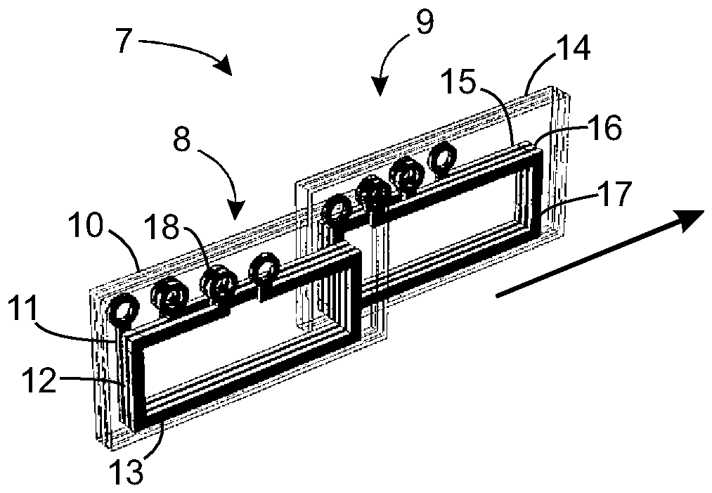
In der
Mittels der an sich bekannten Streuflussmessung lassen sich Materialfehler in Prüflingen
In der
Jede der ersten Leiterschleifen
Wie in der
Nach Einbau der Differenzsonde
Die Differenzsonde
Die beschriebene Differenzsonde
Nach Zerteilen der Platine
Beim Anordnen der Teilabschnitte
BezugszeichenlisteLIST OF REFERENCE NUMBERS
- 1.1.
- PrüfvorrichtungTester
- 2.Second
- RotierkopfRotating
- 3.Third
- DurchgangsöffnungThrough opening
- 4.4th
- Sondeneinrichtungprobe means
- 5.5th
- Sondeneinrichtungprobe means
- 6.6th
- Prüflingexaminee
- 7.7th
- Differenzsondedifferential probe
- 8.8th.
- erste Halbsondefirst half-probe
- 9.9th
- zweite Halbsondesecond half-probe
- 10.10th
- Platinecircuit board
- 11.11th
- erste Leiterschleifefirst conductor loop
- 12.12th
- erste Leiterschleifefirst conductor loop
- 13.13th
- erste Leiterschleifefirst conductor loop
- 14.14th
- Platinecircuit board
- 15.15th
- zweite Leiterschleifesecond conductor loop
- 16.16th
- zweite Leiterschleifesecond conductor loop
- 17.17th
- zweite Leiterschleifesecond conductor loop
- 18.18th
- Kontaktendabschnittcontact end
- 19.19th
- Differenzsondedifferential probe
- 20.20th
- erste Halbsondefirst half-probe
- 21.21st
- zweite Halbsondesecond half-probe
- 22.22nd
- Platinecircuit board
- 23. 23rd
- Teilabschnittpart Of
- 24.24th
- Teilabschnittpart Of
- 25.25th
- Referenzbohrungenreference holes
ZITATE ENTHALTEN IN DER BESCHREIBUNG QUOTES INCLUDE IN THE DESCRIPTION
Diese Liste der vom Anmelder aufgeführten Dokumente wurde automatisiert erzeugt und ist ausschließlich zur besseren Information des Lesers aufgenommen. Die Liste ist nicht Bestandteil der deutschen Patent- bzw. Gebrauchsmusteranmeldung. Das DPMA übernimmt keinerlei Haftung für etwaige Fehler oder Auslassungen.This list of the documents listed by the applicant has been generated automatically and is included solely for the better information of the reader. The list is not part of the German patent or utility model application. The DPMA assumes no liability for any errors or omissions.
Zitierte PatentliteraturCited patent literature
- US 2010/0312494 A1 [0004]US 2010/0312494 A1 [0004]
- EP 1600769 A1 [0004]EP 1600769 A1 [0004]
- US 2011/0057629 A1 [0005]US 2011/0057629 A1 [0005]
Claims (10)
Priority Applications (6)
| Application Number | Priority Date | Filing Date | Title |
|---|---|---|---|
| DE102017107708.1A DE102017107708A1 (en) | 2017-04-10 | 2017-04-10 | Differential probe, testing device and manufacturing process |
| EP18717288.7A EP3583414B1 (en) | 2017-04-10 | 2018-04-04 | Differential probe, testing device and production method |
| JP2019551356A JP2020510217A (en) | 2017-04-10 | 2018-04-04 | Differential probe, inspection device and manufacturing method |
| US16/603,511 US11604167B2 (en) | 2017-04-10 | 2018-04-04 | Differential probe, testing device and production method |
| CN201880020322.9A CN110446922B (en) | 2017-04-10 | 2018-04-04 | Differential probe, probe device and manufacturing method |
| PCT/EP2018/058536 WO2018189000A1 (en) | 2017-04-10 | 2018-04-04 | Differential probe, testing device and production method |
Applications Claiming Priority (1)
| Application Number | Priority Date | Filing Date | Title |
|---|---|---|---|
| DE102017107708.1A DE102017107708A1 (en) | 2017-04-10 | 2017-04-10 | Differential probe, testing device and manufacturing process |
Publications (1)
| Publication Number | Publication Date |
|---|---|
| DE102017107708A1 true DE102017107708A1 (en) | 2018-10-11 |
Family
ID=61965950
Family Applications (1)
| Application Number | Title | Priority Date | Filing Date |
|---|---|---|---|
| DE102017107708.1A Withdrawn DE102017107708A1 (en) | 2017-04-10 | 2017-04-10 | Differential probe, testing device and manufacturing process |
Country Status (6)
| Country | Link |
|---|---|
| US (1) | US11604167B2 (en) |
| EP (1) | EP3583414B1 (en) |
| JP (1) | JP2020510217A (en) |
| CN (1) | CN110446922B (en) |
| DE (1) | DE102017107708A1 (en) |
| WO (1) | WO2018189000A1 (en) |
Families Citing this family (1)
| Publication number | Priority date | Publication date | Assignee | Title |
|---|---|---|---|---|
| JP7359220B2 (en) * | 2020-07-03 | 2023-10-11 | Jfeスチール株式会社 | Sensitivity calibration method, inspection equipment, and magnetic sensor group |
Citations (5)
| Publication number | Priority date | Publication date | Assignee | Title |
|---|---|---|---|---|
| EP1600769A1 (en) | 2004-05-27 | 2005-11-30 | General Electric Company | Omni-directional eddy current probe |
| US20100312494A1 (en) | 2007-12-28 | 2010-12-09 | Sanghamithra Korukonda | Process and apparatus for testing a component using an omni-directional eddy current probe |
| US20110057629A1 (en) | 2009-09-04 | 2011-03-10 | Apple Inc. | Harnessing power through electromagnetic induction utilizing printed coils |
| DE102013209808A1 (en) * | 2013-05-27 | 2014-11-27 | iCONTROLS k.s. | Inductive sensor |
| DE102014212499A1 (en) * | 2014-06-27 | 2015-12-31 | Institut Dr. Foerster Gmbh & Co. Kg | Method and apparatus for leakage flux testing |
Family Cites Families (38)
| Publication number | Priority date | Publication date | Assignee | Title |
|---|---|---|---|---|
| US3504276A (en) * | 1967-04-19 | 1970-03-31 | American Mach & Foundry | Printed circuit coils for use in magnetic flux leakage flow detection |
| US3900793A (en) | 1974-02-25 | 1975-08-19 | Magnetic Analysis Corp | Eddy current testing apparatus including a rotating head with probe and null circuit means mounted thereon including rotary transformer windings |
| JPS63311165A (en) * | 1987-06-12 | 1988-12-19 | Kawasaki Steel Corp | Method and apparatus for finding flaw with magnetism |
| US4873757A (en) | 1987-07-08 | 1989-10-17 | The Foxboro Company | Method of making a multilayer electrical coil |
| JP3041026B2 (en) * | 1990-09-07 | 2000-05-15 | アンリツ株式会社 | Metal detector |
| US5389876A (en) | 1991-05-06 | 1995-02-14 | General Electric Company | Flexible eddy current surface measurement array for detecting near surface flaws in a conductive part |
| US5196796A (en) * | 1991-08-06 | 1993-03-23 | Medrad, Inc. | Anatomically conformal quadrature mri surface coil |
| GB2292223B (en) | 1991-12-20 | 1996-06-26 | Millstrong Ltd | Position measurement |
| CA2076205C (en) | 1992-08-14 | 1999-04-20 | Valentino S. Cecco | Differential transmit-receive eddy current probe incorporating bracelets of multi-coil units |
| DE4410987A1 (en) * | 1994-03-30 | 1995-10-05 | Foerster Inst Dr Friedrich | Eddy current probe for measuring conductor surface irregularities |
| US5659248A (en) * | 1994-10-17 | 1997-08-19 | General Electric Company | Multilayer eddy current probe array for complete coverage of an inspection surface without mechanical scanning |
| JPH0933488A (en) * | 1995-07-20 | 1997-02-07 | Daido Steel Co Ltd | Eddy current flaw detection probe and manufacturing method thereof |
| JP2001305108A (en) * | 2000-04-21 | 2001-10-31 | Daido Steel Co Ltd | Eddy current flaw detector |
| JP2002062280A (en) | 2000-08-22 | 2002-02-28 | Daido Steel Co Ltd | Hot Eddy Current Testing Probe |
| JP4761662B2 (en) * | 2001-07-17 | 2011-08-31 | 三洋電機株式会社 | Circuit device manufacturing method |
| AU2003235382A1 (en) * | 2002-04-26 | 2003-11-10 | Azuma Systems Co., Ltd | Coin shape detection method, coin identification sensor, and coin identification device |
| US7411390B2 (en) | 2002-06-04 | 2008-08-12 | Jentek Sensors, Inc. | High resolution inductive sensor arrays for UXO |
| JP2005221273A (en) * | 2004-02-04 | 2005-08-18 | Daido Steel Co Ltd | Eddy current flaw detection probe, eddy current flaw detection apparatus, and eddy current flaw detection method |
| US20060132123A1 (en) | 2004-12-22 | 2006-06-22 | General Electric Company | Eddy current array probes with enhanced drive fields |
| DE102005047883B4 (en) * | 2005-10-06 | 2008-11-20 | Bruker Biospin Ag | Nuclear magnetic resonance measuring head comprising at least two coils / resonator arrangements with reduced coupling |
| DE102006032268A1 (en) * | 2005-11-01 | 2007-05-10 | Agilent Technologies, Inc. (n.d.Ges.d.Staates Delaware), Palo Alto | Probe e.g. high bandwidth differential probe, for device under test, has differential probe head with replaceable probe tips connected to pair of signal ground elements for representing probed signal |
| JP2009008659A (en) * | 2007-05-25 | 2009-01-15 | Sumitomo Metal Ind Ltd | Surface flaw inspection device |
| US8018228B2 (en) | 2008-06-13 | 2011-09-13 | Olympus Ndt | High resolution and flexible eddy current array probe |
| EP2154495B1 (en) * | 2008-08-15 | 2013-05-22 | Sick Ag | TDR sensor and measuring method |
| US7948233B2 (en) | 2008-10-07 | 2011-05-24 | General Electric Company | Omnidirectional eddy current array probes and methods of use |
| CN102143652B (en) * | 2010-01-30 | 2012-07-18 | 宏恒胜电子科技(淮安)有限公司 | Circuit board |
| FR2965356A1 (en) | 2010-09-23 | 2012-03-30 | Airbus Operations Sas | NON-DESTRUCTIVE CONTROL OF A STRUCTURE IN AN AIRCRAFT |
| JP2013072754A (en) * | 2011-09-28 | 2013-04-22 | Kureyon Co Ltd | Differential type and long-length type of eddy current flaw detection device |
| US8884614B2 (en) | 2011-10-31 | 2014-11-11 | General Electric Company | Eddy current array probe |
| JP2013104761A (en) * | 2011-11-14 | 2013-05-30 | Toyohashi Univ Of Technology | Detector of magnetic metal foreign body |
| DE202013103151U1 (en) | 2012-07-13 | 2013-09-10 | Intelligendt Systems & Services Gmbh | Device for non-destructive eddy current testing of a component |
| DE102013216019A1 (en) | 2013-08-13 | 2015-02-19 | Magnetische Prüfanlagen Gmbh | Multi-layer eddy current probe, method for producing a multi-layer eddy current probe and multi-layer eddy current probe tester |
| US9651576B2 (en) * | 2013-10-17 | 2017-05-16 | Thermo Keytek LLC | Low-side coaxial current probe |
| JP5922633B2 (en) * | 2013-10-22 | 2016-05-24 | 三菱重工業株式会社 | Eddy current flaw detection probe and eddy current flaw detection method |
| US9322806B2 (en) | 2013-10-25 | 2016-04-26 | General Electric Company | Eddy current sensor with linear drive conductor |
| US20170299666A1 (en) * | 2014-11-17 | 2017-10-19 | Halliburton Energy Services, Inc. | Rapid Magnetic Hotspot Detector |
| CN104820015B (en) * | 2015-05-08 | 2018-05-15 | 北京华航无线电测量研究所 | A kind of cracks of metal surface detecting system and its detection method |
| CN106483480B (en) * | 2016-09-26 | 2019-06-25 | 中国人民解放军国防科学技术大学 | Single probe biological magnetic field detection method, circuit and sensor based on GMI effect |
-
2017
- 2017-04-10 DE DE102017107708.1A patent/DE102017107708A1/en not_active Withdrawn
-
2018
- 2018-04-04 EP EP18717288.7A patent/EP3583414B1/en active Active
- 2018-04-04 WO PCT/EP2018/058536 patent/WO2018189000A1/en not_active Ceased
- 2018-04-04 CN CN201880020322.9A patent/CN110446922B/en active Active
- 2018-04-04 US US16/603,511 patent/US11604167B2/en active Active
- 2018-04-04 JP JP2019551356A patent/JP2020510217A/en active Pending
Patent Citations (5)
| Publication number | Priority date | Publication date | Assignee | Title |
|---|---|---|---|---|
| EP1600769A1 (en) | 2004-05-27 | 2005-11-30 | General Electric Company | Omni-directional eddy current probe |
| US20100312494A1 (en) | 2007-12-28 | 2010-12-09 | Sanghamithra Korukonda | Process and apparatus for testing a component using an omni-directional eddy current probe |
| US20110057629A1 (en) | 2009-09-04 | 2011-03-10 | Apple Inc. | Harnessing power through electromagnetic induction utilizing printed coils |
| DE102013209808A1 (en) * | 2013-05-27 | 2014-11-27 | iCONTROLS k.s. | Inductive sensor |
| DE102014212499A1 (en) * | 2014-06-27 | 2015-12-31 | Institut Dr. Foerster Gmbh & Co. Kg | Method and apparatus for leakage flux testing |
Also Published As
| Publication number | Publication date |
|---|---|
| EP3583414A1 (en) | 2019-12-25 |
| WO2018189000A1 (en) | 2018-10-18 |
| JP2020510217A (en) | 2020-04-02 |
| US20200041453A1 (en) | 2020-02-06 |
| CN110446922A (en) | 2019-11-12 |
| EP3583414B1 (en) | 2021-02-24 |
| US11604167B2 (en) | 2023-03-14 |
| CN110446922B (en) | 2024-04-02 |
Similar Documents
| Publication | Publication Date | Title |
|---|---|---|
| DE102007046054B4 (en) | Improved high-precision Rogowski current transformer | |
| EP3479071B1 (en) | Angle position sensor, stator element and rotorelement therefor | |
| DE60116079T2 (en) | CURRENT MEASURING DEVICE | |
| EP2037286A1 (en) | Measuring device for measuring a magnetic field | |
| DE102008006865A1 (en) | Inductive torque sensor | |
| EP3500825B1 (en) | Sensor system and method for determining the absolute angle position of a shaft, and vehicle with such sensor system | |
| DE2509927C3 (en) | Eddy current test coil arrangement | |
| DE3621107C2 (en) | ||
| DE19527921A1 (en) | Double-sided HF screen for coil in set of gradient coils | |
| WO2013124087A1 (en) | Through-coil arrangement, test apparatus with through-coil arrangement and testing method | |
| EP0838688A2 (en) | Device and procedure for testing printed circuit boards | |
| DE102013222523A1 (en) | Eddy current probe and eddy current tester | |
| DE102013216019A1 (en) | Multi-layer eddy current probe, method for producing a multi-layer eddy current probe and multi-layer eddy current probe tester | |
| DE2626060A1 (en) | EDDY CURRENT PROBE FOR NON-DESTRUCTION-FREE MATERIAL TESTING | |
| EP0772054B1 (en) | Method and device for testing an electric conductor arrangement | |
| DE2701857C2 (en) | ||
| DE2906736C2 (en) | Device for testing electrical circuit boards | |
| EP3583414B1 (en) | Differential probe, testing device and production method | |
| DE3725718A1 (en) | SAMPLE HEAD FOR NMR SPECTROMETER | |
| DE2653923B2 (en) | Device for material testing with an electrodynamic converter | |
| DE102016219620A1 (en) | A printed circuit board with a bent connection portion and method of testing the same, and electronic control apparatus and method of operating the same | |
| DE69935610T2 (en) | USE OF AN ELECTRIC FAIR ELEMENT | |
| DE4312862A1 (en) | Rotatable capacitance sensor | |
| DE102018105857A1 (en) | Apparatus for measuring electricity and method of manufacture | |
| DE2232081A1 (en) | PROCEDURE FOR DETERMINING DISCONTINUITIES IN METALLIC DUTIES |
Legal Events
| Date | Code | Title | Description |
|---|---|---|---|
| R079 | Amendment of ipc main class |
Free format text: PREVIOUS MAIN CLASS: G01N0027900000 Ipc: G01N0027820000 |
|
| R163 | Identified publications notified | ||
| R081 | Change of applicant/patentee |
Owner name: PRUEFTECHNIK DIETER BUSCH GMBH, DE Free format text: FORMER OWNER: PRUEFTECHNIK DIETER BUSCH AG, 85737 ISMANING, DE |
|
| R119 | Application deemed withdrawn, or ip right lapsed, due to non-payment of renewal fee |