[go: up one dir, main page]

DE102016225271A1 - Organometallic complex, light-emitting element, light-emitting device, electronic device and lighting device - Google Patents

Organometallic complex, light-emitting element, light-emitting device, electronic device and lighting device Download PDF

Info

Publication number
DE102016225271A1
DE102016225271A1 DE102016225271.2A DE102016225271A DE102016225271A1 DE 102016225271 A1 DE102016225271 A1 DE 102016225271A1 DE 102016225271 A DE102016225271 A DE 102016225271A DE 102016225271 A1 DE102016225271 A1 DE 102016225271A1
Authority
DE
Germany
Prior art keywords
carbon atoms
substituted
group
light
unsubstituted
Prior art date
Legal status (The legal status is an assumption and is not a legal conclusion. Google has not performed a legal analysis and makes no representation as to the accuracy of the status listed.)
Pending
Application number
DE102016225271.2A
Other languages
German (de)
Inventor
Tomoya Yamaguchi
Hideko Inoue
Hiromitsu KIDO
Satoshi Seo
Tatsuyoshi Takahashi
Current Assignee (The listed assignees may be inaccurate. Google has not performed a legal analysis and makes no representation or warranty as to the accuracy of the list.)
Semiconductor Energy Laboratory Co Ltd
Original Assignee
Semiconductor Energy Laboratory Co Ltd
Priority date (The priority date is an assumption and is not a legal conclusion. Google has not performed a legal analysis and makes no representation as to the accuracy of the date listed.)
Filing date
Publication date
Application filed by Semiconductor Energy Laboratory Co Ltd filed Critical Semiconductor Energy Laboratory Co Ltd
Publication of DE102016225271A1 publication Critical patent/DE102016225271A1/en
Pending legal-status Critical Current

Links

Images

Classifications

    • HELECTRICITY
    • H10SEMICONDUCTOR DEVICES; ELECTRIC SOLID-STATE DEVICES NOT OTHERWISE PROVIDED FOR
    • H10KORGANIC ELECTRIC SOLID-STATE DEVICES
    • H10K85/00Organic materials used in the body or electrodes of devices covered by this subclass
    • H10K85/30Coordination compounds
    • H10K85/341Transition metal complexes, e.g. Ru(II)polypyridine complexes
    • H10K85/342Transition metal complexes, e.g. Ru(II)polypyridine complexes comprising iridium
    • CCHEMISTRY; METALLURGY
    • C07ORGANIC CHEMISTRY
    • C07FACYCLIC, CARBOCYCLIC OR HETEROCYCLIC COMPOUNDS CONTAINING ELEMENTS OTHER THAN CARBON, HYDROGEN, HALOGEN, OXYGEN, NITROGEN, SULFUR, SELENIUM OR TELLURIUM
    • C07F15/00Compounds containing elements of Groups 8, 9, 10 or 18 of the Periodic Table
    • C07F15/0006Compounds containing elements of Groups 8, 9, 10 or 18 of the Periodic Table compounds of the platinum group
    • C07F15/0033Iridium compounds
    • C07F15/004Iridium compounds without a metal-carbon linkage
    • CCHEMISTRY; METALLURGY
    • C09DYES; PAINTS; POLISHES; NATURAL RESINS; ADHESIVES; COMPOSITIONS NOT OTHERWISE PROVIDED FOR; APPLICATIONS OF MATERIALS NOT OTHERWISE PROVIDED FOR
    • C09KMATERIALS FOR MISCELLANEOUS APPLICATIONS, NOT PROVIDED FOR ELSEWHERE
    • C09K11/00Luminescent, e.g. electroluminescent, chemiluminescent materials
    • C09K11/06Luminescent, e.g. electroluminescent, chemiluminescent materials containing organic luminescent materials
    • CCHEMISTRY; METALLURGY
    • C09DYES; PAINTS; POLISHES; NATURAL RESINS; ADHESIVES; COMPOSITIONS NOT OTHERWISE PROVIDED FOR; APPLICATIONS OF MATERIALS NOT OTHERWISE PROVIDED FOR
    • C09KMATERIALS FOR MISCELLANEOUS APPLICATIONS, NOT PROVIDED FOR ELSEWHERE
    • C09K2211/00Chemical nature of organic luminescent or tenebrescent compounds
    • C09K2211/10Non-macromolecular compounds
    • C09K2211/1003Carbocyclic compounds
    • C09K2211/1007Non-condensed systems
    • CCHEMISTRY; METALLURGY
    • C09DYES; PAINTS; POLISHES; NATURAL RESINS; ADHESIVES; COMPOSITIONS NOT OTHERWISE PROVIDED FOR; APPLICATIONS OF MATERIALS NOT OTHERWISE PROVIDED FOR
    • C09KMATERIALS FOR MISCELLANEOUS APPLICATIONS, NOT PROVIDED FOR ELSEWHERE
    • C09K2211/00Chemical nature of organic luminescent or tenebrescent compounds
    • C09K2211/10Non-macromolecular compounds
    • C09K2211/1018Heterocyclic compounds
    • C09K2211/1025Heterocyclic compounds characterised by ligands
    • C09K2211/1029Heterocyclic compounds characterised by ligands containing one nitrogen atom as the heteroatom
    • CCHEMISTRY; METALLURGY
    • C09DYES; PAINTS; POLISHES; NATURAL RESINS; ADHESIVES; COMPOSITIONS NOT OTHERWISE PROVIDED FOR; APPLICATIONS OF MATERIALS NOT OTHERWISE PROVIDED FOR
    • C09KMATERIALS FOR MISCELLANEOUS APPLICATIONS, NOT PROVIDED FOR ELSEWHERE
    • C09K2211/00Chemical nature of organic luminescent or tenebrescent compounds
    • C09K2211/10Non-macromolecular compounds
    • C09K2211/1018Heterocyclic compounds
    • C09K2211/1025Heterocyclic compounds characterised by ligands
    • C09K2211/1044Heterocyclic compounds characterised by ligands containing two nitrogen atoms as heteroatoms
    • CCHEMISTRY; METALLURGY
    • C09DYES; PAINTS; POLISHES; NATURAL RESINS; ADHESIVES; COMPOSITIONS NOT OTHERWISE PROVIDED FOR; APPLICATIONS OF MATERIALS NOT OTHERWISE PROVIDED FOR
    • C09KMATERIALS FOR MISCELLANEOUS APPLICATIONS, NOT PROVIDED FOR ELSEWHERE
    • C09K2211/00Chemical nature of organic luminescent or tenebrescent compounds
    • C09K2211/18Metal complexes
    • C09K2211/185Metal complexes of the platinum group, i.e. Os, Ir, Pt, Ru, Rh or Pd
    • HELECTRICITY
    • H10SEMICONDUCTOR DEVICES; ELECTRIC SOLID-STATE DEVICES NOT OTHERWISE PROVIDED FOR
    • H10KORGANIC ELECTRIC SOLID-STATE DEVICES
    • H10K2101/00Properties of the organic materials covered by group H10K85/00
    • H10K2101/10Triplet emission
    • HELECTRICITY
    • H10SEMICONDUCTOR DEVICES; ELECTRIC SOLID-STATE DEVICES NOT OTHERWISE PROVIDED FOR
    • H10KORGANIC ELECTRIC SOLID-STATE DEVICES
    • H10K2101/00Properties of the organic materials covered by group H10K85/00
    • H10K2101/90Multiple hosts in the emissive layer
    • HELECTRICITY
    • H10SEMICONDUCTOR DEVICES; ELECTRIC SOLID-STATE DEVICES NOT OTHERWISE PROVIDED FOR
    • H10KORGANIC ELECTRIC SOLID-STATE DEVICES
    • H10K50/00Organic light-emitting devices
    • H10K50/10OLEDs or polymer light-emitting diodes [PLED]
    • H10K50/11OLEDs or polymer light-emitting diodes [PLED] characterised by the electroluminescent [EL] layers
    • HELECTRICITY
    • H10SEMICONDUCTOR DEVICES; ELECTRIC SOLID-STATE DEVICES NOT OTHERWISE PROVIDED FOR
    • H10KORGANIC ELECTRIC SOLID-STATE DEVICES
    • H10K85/00Organic materials used in the body or electrodes of devices covered by this subclass
    • H10K85/60Organic compounds having low molecular weight
    • H10K85/631Amine compounds having at least two aryl rest on at least one amine-nitrogen atom, e.g. triphenylamine
    • H10K85/633Amine compounds having at least two aryl rest on at least one amine-nitrogen atom, e.g. triphenylamine comprising polycyclic condensed aromatic hydrocarbons as substituents on the nitrogen atom
    • HELECTRICITY
    • H10SEMICONDUCTOR DEVICES; ELECTRIC SOLID-STATE DEVICES NOT OTHERWISE PROVIDED FOR
    • H10KORGANIC ELECTRIC SOLID-STATE DEVICES
    • H10K85/00Organic materials used in the body or electrodes of devices covered by this subclass
    • H10K85/60Organic compounds having low molecular weight
    • H10K85/649Aromatic compounds comprising a hetero atom
    • H10K85/657Polycyclic condensed heteroaromatic hydrocarbons
    • H10K85/6572Polycyclic condensed heteroaromatic hydrocarbons comprising only nitrogen in the heteroaromatic polycondensed ring system, e.g. phenanthroline or carbazole
    • HELECTRICITY
    • H10SEMICONDUCTOR DEVICES; ELECTRIC SOLID-STATE DEVICES NOT OTHERWISE PROVIDED FOR
    • H10KORGANIC ELECTRIC SOLID-STATE DEVICES
    • H10K85/00Organic materials used in the body or electrodes of devices covered by this subclass
    • H10K85/60Organic compounds having low molecular weight
    • H10K85/649Aromatic compounds comprising a hetero atom
    • H10K85/657Polycyclic condensed heteroaromatic hydrocarbons
    • H10K85/6576Polycyclic condensed heteroaromatic hydrocarbons comprising only sulfur in the heteroaromatic polycondensed ring system, e.g. benzothiophene
    • YGENERAL TAGGING OF NEW TECHNOLOGICAL DEVELOPMENTS; GENERAL TAGGING OF CROSS-SECTIONAL TECHNOLOGIES SPANNING OVER SEVERAL SECTIONS OF THE IPC; TECHNICAL SUBJECTS COVERED BY FORMER USPC CROSS-REFERENCE ART COLLECTIONS [XRACs] AND DIGESTS
    • Y02TECHNOLOGIES OR APPLICATIONS FOR MITIGATION OR ADAPTATION AGAINST CLIMATE CHANGE
    • Y02PCLIMATE CHANGE MITIGATION TECHNOLOGIES IN THE PRODUCTION OR PROCESSING OF GOODS
    • Y02P20/00Technologies relating to chemical industry
    • Y02P20/50Improvements relating to the production of bulk chemicals
    • Y02P20/582Recycling of unreacted starting or intermediate materials

Landscapes

  • Chemical & Material Sciences (AREA)
  • Organic Chemistry (AREA)
  • Engineering & Computer Science (AREA)
  • Materials Engineering (AREA)
  • Crystallography & Structural Chemistry (AREA)
  • Inorganic Chemistry (AREA)
  • Electroluminescent Light Sources (AREA)
  • Low-Molecular Organic Synthesis Reactions Using Catalysts (AREA)
  • Organic Low-Molecular-Weight Compounds And Preparation Thereof (AREA)

Abstract

Ein neuartiger metallorganischer Komplex mit einer hohen Wärmebeständigkeit wird bereitgestellt. Der metallorganische Komplex, der eine Struktur umfasst, die durch die allgemeine Formel (G1) dargestellt wird, umfasst Iridium und einen Liganden. Der Ligand weist ein Pyrazin-Gerüst auf. Iridium ist an Stickstoff an der 1-Position des Pyrazin-Gerüsts gebunden. Eine Phenyl-Gruppe, die eine Alkyl-Gruppe als Substituenten aufweist, ist jeweils an die 2- und 3-Position des Pyrazin-Gerüsts gebunden, und eine Phenyl-Gruppe, die eine Cyano-Gruppe als Substituenten aufweist, ist an die 5-Position des Pyrazin-Gerüsts gebunden. Die ortho-Position der Phenyl-Gruppe, die an die 2-Position des Pyrazin-Gerüsts gebunden ist, ist an Iridium gebunden.In der Formel stellen A1 bis A4 jeweils unabhängig voneinander eine substituierte oder nicht substituierte Alkyl-Gruppe mit 1 bis 6 Kohlenstoffatomen dar. R1 bis R6 stellen jeweils unabhängig voneinander Wasserstoff, eine substituierte oder nicht substituierte Alkyl-Gruppe mit 1 bis 6 Kohlenstoffatomen, eine substituierte oder nicht substituierte Aryl-Gruppe mit 6 bis 13 Kohlenstoffatomen oder eine substituierte oder nicht substituierte Heteroaryl-Gruppe mit 3 bis 12 Kohlenstoffatomen dar. R7 bis R11 stellen jeweils unabhängig voneinander Wasserstoff, eine substituierte oder nicht substituierte Alkyl-Gruppe mit 1 bis 6 Kohlenstoffatomen, eine substituierte oder nicht substituierte Aryl-Gruppe mit 6 bis 13 Kohlenstoffatomen, eine substituierte oder nicht substituierte Heteroaryl-Gruppe mit 3 bis 12 Kohlenstoffatomen oder eine Cyano-Gruppe dar. Mindestens eines von R7 bis R11 stellt eine Cyano-Gruppe dar.A novel organometallic complex having a high heat resistance is provided. The organometallic complex comprising a structure represented by the general formula (G1) includes iridium and a ligand. The ligand has a pyrazine skeleton. Iridium is bound to nitrogen at the 1-position of the pyrazine backbone. A phenyl group having an alkyl group as a substituent is bonded respectively to the 2- and 3-positions of the pyrazine skeleton, and a phenyl group having a cyano group as a substituent is attached to the 5- Position of the pyrazine skeleton bound. The ortho position of the phenyl group bonded to the 2-position of the pyrazine skeleton is bonded to iridium. In the formula, A1 to A4 each independently represent a substituted or unsubstituted alkyl group having 1 to 6 carbon atoms R1 to R6 each independently represent hydrogen, a substituted or unsubstituted alkyl group of 1 to 6 carbon atoms, a substituted or unsubstituted aryl group of 6 to 13 carbon atoms or a substituted or unsubstituted heteroaryl group of 3 to R7 to R11 each independently represent hydrogen, a substituted or unsubstituted alkyl group of 1 to 6 carbon atoms, a substituted or unsubstituted aryl group of 6 to 13 carbon atoms, a substituted or unsubstituted heteroaryl group 3 to 12 carbon atoms or a cyano group. At least one of R7 to R11 represents a cyano group.

Description

Hintergrund der ErfindungBackground of the invention

1. Gebiet der Erfindung1. Field of the invention

Eine Ausführungsform der vorliegenden Erfindung betrifft einen metallorganischen Komplex. Insbesondere betrifft eine Ausführungsform der vorliegenden Erfindung einen metallorganischen Komplex, der Triplett-Anregungsenergie in Lichtemission umwandeln kann. Darüber hinaus betrifft eine Ausführungsform der vorliegenden Erfindung ein Licht emittierendes Element, eine Licht emittierende Vorrichtung, ein elektronisches Gerät und eine Beleuchtungsvorrichtung, die jeweils den metallorganischen Komplex umfassen. Es sei angemerkt, dass eine Ausführungsform der vorliegenden Erfindung nicht auf das vorstehende technische Gebiet beschränkt ist. Das technische Gebiet einer Ausführungsform der Erfindung, die in dieser Beschreibung und dergleichen offenbart wird, betrifft einen Gegenstand, ein Verfahren oder ein Herstellungsverfahren. Eine Ausführungsform der vorliegenden Erfindung betrifft zusätzlich einen Prozess, eine Maschine, ein Erzeugnis oder eine Zusammensetzung. Konkrete Beispiele für das technische Gebiet einer Ausführungsform der in dieser Beschreibung offenbarten vorliegenden Erfindung umfassen neben dem Vorstehenden eine Halbleitervorrichtung, eine Anzeigevorrichtung, eine Flüssigkristallanzeigevorrichtung, eine Energiespeichervorrichtung, eine Speichervorrichtung, ein Verfahren zum Betreiben einer von ihnen und ein Verfahren zum Herstellen einer von ihnen.One embodiment of the present invention relates to an organometallic complex. In particular, one embodiment of the present invention relates to an organometallic complex capable of converting triplet excitation energy into light emission. Moreover, an embodiment of the present invention relates to a light-emitting element, a light-emitting device, an electronic device, and a lighting device each comprising the organometallic complex. It should be noted that an embodiment of the present invention is not limited to the above technical field. The technical field of an embodiment of the invention disclosed in this specification and the like relates to an article, a method or a manufacturing method. An embodiment of the present invention additionally relates to a process, a machine, a product or a composition. Concrete examples of the technical field of an embodiment of the present invention disclosed in this specification include, in addition to the above, a semiconductor device, a display device, a liquid crystal display device, an energy storage device, a storage device, a method of operating one of them, and a method of manufacturing one of them.

2. Beschreibung des technischen Gebiets2. Description of the technical field

Eine Anzeige, die ein Licht emittierendes Element mit einer Struktur umfasst, bei der eine organische Verbindung, bei der es sich um eine Licht emittierende Substanz handelt, zwischen einem Paar von Elektroden bereitgestellt ist (auch als organisches EL-Element bezeichnet), hat als Flachbildschirmanzeige der nächsten Generation in Hinblick auf die Eigenschaften des Licht emittierenden Elements, wie z. B. dünn und leichtgewichtig zu sein, eine hohe Ansprechgeschwindigkeit und eine niedrige Ansteuerspannung aufzuweisen, Aufmerksamkeit auf sich gezogen. Wenn eine Spannung an dieses Licht emittierende Element angelegt wird, rekombinieren Elektronen und Löcher, die von den Elektroden injiziert werden, wodurch die Licht emittierende Substanz in einen Anregungszustand versetzt wird, und dann wird Licht emittiert, wenn diese von dem Anregungszustand in den Grundzustand zurückkehrt. Bei dem Anregungszustand kann es sich um einen Singulett-Anregungszustand (S*) oder einen Triplett-Anregungszustand (T*) handeln. Lichtemission von einem Singulett-Anregungszustand wird als Fluoreszenz bezeichnet, und Lichtemission von einem Triplett-Anregungszustand wird als Phosphoreszenz bezeichnet. Es wird davon ausgegangen, dass das statistische Erzeugungsverhältnis dieser in dem Licht emittierenden Element S*:T* = 1:3 ist.A display comprising a light-emitting element having a structure in which an organic compound which is a light-emitting substance is provided between a pair of electrodes (also referred to as an organic EL element) has a flat-panel display the next generation in terms of the properties of the light-emitting element, such as. For example, to be thin and lightweight, have a high response speed, and a low drive voltage, attention has been drawn. When a voltage is applied to this light-emitting element, electrons and holes injected from the electrodes recombine, thereby putting the light-emitting substance in an excited state, and then light is emitted as it returns from the excited state to the ground state. The excited state may be a singlet excited state (S *) or a triplet excited state (T *). Light emission from a singlet excited state is referred to as fluorescence, and light emission from a triplet excited state is referred to as phosphorescence. It is assumed that the statistical production ratio of these in the light-emitting element is S *: T * = 1: 3.

Unter den vorstehenden Licht emittierenden Substanzen wird eine Verbindung, die Singulett-Anregungsenergie in Lichtemission umwandeln kann als fluoreszierende Verbindung (fluoreszierendes Material) bezeichnet, und eine Verbindung, die Triplett-Anregungsenergie in Lichtemission umwandeln kann, wird als phosphoreszierende Verbindung (phosphoreszierendes Material) bezeichnet.Among the above light-emitting substances, a compound capable of converting singlet excitation energy into light emission is called a fluorescent compound (fluorescent material), and a compound capable of converting triplet excitation energy to light emission is called a phosphorescent material.

Auf Basis des vorstehenden Erzeugungsverhältnisses wird davon ausgegangen, dass die interne Quanteneffizienz (das Verhältnis von der Anzahl der erzeugten Photonen zu der Anzahl von injizierten Ladungsträgern) eines Licht emittierenden Elements, das ein fluoreszierendes Material umfasst, eine theoretische Grenze von 25% aufweist, wohingegen davon ausgegangen wird, dass die interne Quanteneffizienz eines Licht emittierenden Elements, das ein phosphoreszierendes Material umfasst, eine theoretische Grenze von 75% aufweist.Based on the above generation ratio, it is considered that the internal quantum efficiency (the ratio of the number of photons generated to the number of injected carriers) of a light-emitting element comprising a fluorescent material has a theoretical limit of 25%, whereas It is assumed that the internal quantum efficiency of a light-emitting element comprising a phosphorescent material has a theoretical limit of 75%.

Mit anderen Worten: Ein Licht emittierendes Element, das ein phosphoreszierendes Material umfasst, weist eine höhere Effizienz auf als ein Licht emittierendes Element, das ein fluoreszierendes Material umfasst. Demzufolge wurden verschiedene Arten von phosphoreszierenden Materialien in den letzten Jahren aktiv entwickelt. Ein metallorganischer Komplex, der Iridium oder dergleichen als Zentralmetall enthält, hat insbesondere auf Grund seiner hohen Phosphoreszenz-Quantenausbeute Aufmerksamkeit auf sich gezogen (siehe beispielsweise Patentdokument 1).In other words, a light-emitting element comprising a phosphorescent material has a higher efficiency than a light-emitting element comprising a fluorescent material. As a result, various types of phosphorescent materials have been actively developed in recent years. An organometallic complex containing iridium or the like as the central metal has been attracting attention in particular because of its high phosphorescence quantum yield (see, for example, Patent Document 1).

[Referenz] [Reference]

[Patentdokument][Patent Document]

  • [Patentdokument 1] Japanische Patentoffenlegungsschrift Nr. 2009-023938 [Patent Document 1] Japanese Patent Laid-Open Publication No. 2009-023938

Zusammenfassung der ErfindungSummary of the invention

Obwohl, wie im Patentdokument 1 offenbart, phosphoreszierende Materialien mit ausgezeichneten Eigenschaften aktiv entwickelt worden sind, wird die Entwicklung neuartiger Materialen mit besseren Eigenschaften gefordert.Although, as disclosed in Patent Document 1, phosphorescent materials having excellent properties have been actively developed, the development of novel materials having superior properties is demanded.

In Anbetracht des Vorstehenden wird entsprechend einer Ausführungsform der vorliegenden Erfindung ein neuartiger metallorganischer Komplex bereitgestellt. Entsprechend einer Ausführungsform der vorliegenden Erfindung wird ein neuartiger metallorganischer Komplex mit einer hohen Wärmebeständigkeit bereitgestellt. Entsprechend einer Ausführungsform der vorliegenden Erfindung wird ein neuartiger metallorganischer Komplex bereitgestellt, der bei einer Sublimation weniger zersetzt wird. Entsprechend einer Ausführungsform der vorliegenden Erfindung wird ein neuartiger metallorganischer Komplex mit einer hohen Farbreinheit bereitgestellt. Entsprechend einer Ausführungsform der vorliegenden Erfindung wird ein neuartiger metallorganischer Komplex, der bei einem Licht emittierenden Element verwendet werden kann, bereitgestellt. Entsprechend einer Ausführungsform der vorliegenden Erfindung wird ein neuartiger metallorganischer Komplex, der bei einer EL-Schicht eines Licht emittierenden Elements verwendet werden kann, bereitgestellt. Entsprechend einer Ausführungsform der vorliegenden Erfindung wird ein neuartiges Licht emittierendes Element bereitgestellt. Entsprechend einer Ausführungsform der vorliegenden Erfindung wird außerdem eine neuartige Licht emittierende Vorrichtung, ein neuartiges elektronisches Gerät oder eine neuartige Beleuchtungsvorrichtung bereitgestellt. Es sei angemerkt, dass die Beschreibungen dieser Aufgaben dem Vorhandensein weiterer Aufgaben nicht im Weg stehen. Bei einer Ausführungsform der vorliegenden Erfindung ist es unnötig, sämtliche der Aufgaben zu erfüllen. Weitere Aufgaben werden aus der Erläuterung der Beschreibung, der Zeichnungen, der Patentansprüche und dergleichen ersichtlich und können davon abgeleitet werden.In view of the foregoing, according to one embodiment of the present invention, there is provided a novel organometallic complex. According to one embodiment of the present invention, there is provided a novel organometallic complex having a high heat resistance. According to one embodiment of the present invention, there is provided a novel organometallic complex which is less decomposed in a sublimation. According to one embodiment of the present invention, a novel organometallic complex having a high color purity is provided. According to one embodiment of the present invention, a novel organometallic complex which can be used in a light-emitting element is provided. According to an embodiment of the present invention, there is provided a novel organometallic complex which can be used in an EL layer of a light-emitting element. According to an embodiment of the present invention, a novel light-emitting element is provided. According to an embodiment of the present invention, there is also provided a novel light-emitting device, a novel electronic device or a novel lighting device. It should be noted that the descriptions of these tasks do not stand in the way of the existence of further tasks. In one embodiment of the present invention, it is unnecessary to accomplish all of the tasks. Other objects will become apparent from the description of the specification, the drawings, the claims and the like, and may be derived therefrom.

Eine Ausführungsform der vorliegenden Erfindung ist ein metallorganischer Komplex, der Iridium und einen Liganden umfasst. Der Ligand weist ein Pyrazin-Gerüst auf. Iridium ist an Stickstoff an der 1-Position des Pyrazin-Gerüsts gebunden. Eine Phenyl-Gruppe ist jeweils an die 2-, 3- und 5-Position des Pyrazin-Gerüsts gebunden. Die Phenyl-Gruppen, die an die 2- und 3-Position gebunden sind, weisen jeweils eine Alkyl-Gruppe als Substituenten auf. Die Phenyl-Gruppe, die an die 5-Position gebunden ist, weist eine Cyano-Gruppe als Substituenten auf.One embodiment of the present invention is an organometallic complex comprising iridium and a ligand. The ligand has a pyrazine skeleton. Iridium is bound to nitrogen at the 1-position of the pyrazine backbone. Each phenyl group is attached to the 2-, 3- and 5-position of the pyrazine skeleton. The phenyl groups attached to the 2- and 3-positions each have an alkyl group as a substituent. The phenyl group attached to the 5-position has a cyano group as a substituent.

Eine weitere Ausführungsform der vorliegenden Erfindung ist ein metallorganischer Komplex, der einen ersten Liganden und einen zweiten Liganden umfasst, die an Iridium gebunden sind. Der erste Ligand weist ein Pyrazin-Gerüst auf. Iridium ist an Stickstoff an der 1-Position des Pyrazin-Gerüsts gebunden. Eine Phenyl-Gruppe ist jeweils an die 2-, 3- und 5-Position des Pyrazin-Gerüsts gebunden. Die Phenyl-Gruppen, die an die 2- und 3-Position gebunden sind, weisen jeweils eine Alkyl-Gruppe als Substituenten auf. Die Phenyl-Gruppe, die an die 5-Position gebunden ist, weist eine Cyano-Gruppe als Substituenten auf. Der zweite Ligand ist ein monoanionischer Ligand. Insbesondere handelt es sich bei dem zweiten Liganden vorzugsweise um einen monoanionischen zweizähnigen Chelat-Liganden mit einer β-Diketon-Struktur, einen monoanionischen zweizähnigen Chelat-Liganden mit einer Carboxyl-Gruppe, einen monoanionischen zweizähnigen Chelat-Liganden mit einer phenolischen Hydroxyl-Gruppe, einen monoanionischen zweizähnigen Chelat-Liganden, bei dem zwei koordinierte Elemente jeweils Stickstoff sind, oder einen aromatischen heterocyclischen zweizähnigen Liganden, der durch Cyclometallierung eine Metall-Kohlenstoff-Bindung mit Iridium bilden kann.Another embodiment of the present invention is an organometallic complex comprising a first ligand and a second ligand bound to iridium. The first ligand has a pyrazine backbone. Iridium is bound to nitrogen at the 1-position of the pyrazine backbone. Each phenyl group is attached to the 2-, 3- and 5-position of the pyrazine skeleton. The phenyl groups attached to the 2- and 3-positions each have an alkyl group as a substituent. The phenyl group attached to the 5-position has a cyano group as a substituent. The second ligand is a monoanionic ligand. In particular, the second ligand is preferably a monoanionic bidentate chelate ligand having a β-diketone structure, a monoanionic bidentate chelate ligand having a carboxyl group, a monoanionic bidentate chelate ligand having a phenolic hydroxyl group, a monoanionic bidentate chelate ligands, in which two coordinated elements are each nitrogen, or an aromatic heterocyclic bidentate ligand, which can form a metal-carbon bond with iridium by cyclometalation.

Es sei angemerkt, dass bei der vorstehenden Struktur die Phenyl-Gruppe, die an die 5-Position des Pyrazin-Gerüsts gebunden ist, vorzugsweise ferner eine Alkyl-Gruppe aufweist. Eine Alkyl-Gruppe, die an mindestens der 2-Position der Phenyl-Gruppe eingeführt wird, die an die 5-Position des Pyrazin-Gerüsts gebunden ist, kann insbesondere verhindern, dass sich ein Emissionsspektrum zu sehr zu einer langen Wellenlängenseite hin verschiebt, und kann einen Leuchtstärkefaktor aufrechterhalten. Das heißt: Diese Struktur ist insbesondere dafür geeignet, eine hohe Farbreinheit und eine tiefrote Emission mit hoher Effizienz zu erzielen.It should be noted that in the above structure, the phenyl group bonded to the 5-position of the pyrazine skeleton preferably further has an alkyl group. In particular, an alkyl group introduced at at least the 2-position of the phenyl group bonded to the 5-position of the pyrazine skeleton can prevent an emission spectrum from shifting too much toward a long wavelength side, and can maintain a luminance factor. That is, this structure is particularly suitable for achieving high color purity and deep red emission with high efficiency.

Eine weitere Ausführungsform der vorliegenden Erfindung ist ein metallorganischer Komplex, der eine Struktur umfasst, die durch die folgende allgemeine Formel (G1) dargestellt wird.

Figure DE102016225271A1_0003
Another embodiment of the present invention is an organometallic complex comprising a structure represented by the following general formula (G1).
Figure DE102016225271A1_0003

Es sei angemerkt, dass in der allgemeinen Formel (G1) A1 bis A4 jeweils unabhängig voneinander eine substituierte oder nicht substituierte Alkyl-Gruppe mit 1 bis 6 Kohlenstoffatomen darstellen. R1 bis R6 stellen jeweils unabhängig voneinander Wasserstoff, eine substituierte oder nicht substituierte Alkyl-Gruppe mit 1 bis 6 Kohlenstoffatomen, eine substituierte oder nicht substituierte Aryl-Gruppe mit 6 bis 13 Kohlenstoffatomen oder eine substituierte oder nicht substituierte Heteroaryl-Gruppe mit 3 bis 12 Kohlenstoffatomen dar. R7 bis R11 stellen jeweils unabhängig voneinander Wasserstoff, eine substituierte oder nicht substituierte Alkyl-Gruppe mit 1 bis 6 Kohlenstoffatomen, eine substituierte oder nicht substituierte Aryl-Gruppe mit 6 bis 13 Kohlenstoffatomen, eine substituierte oder nicht substituierte Heteroaryl-Gruppe mit 3 bis 12 Kohlenstoffatomen oder eine Cyano-Gruppe dar. Mindestens eines von R7 bis R11 stellt eine Cyano-Gruppe dar.It should be noted that in the general formula (G1), A 1 to A 4 each independently represent a substituted or unsubstituted alkyl group having 1 to 6 carbon atoms. R 1 to R 6 each independently represent hydrogen, a substituted or unsubstituted alkyl group of 1 to 6 carbon atoms, a substituted or unsubstituted aryl group of 6 to 13 carbon atoms or a substituted or unsubstituted heteroaryl group of 3 to R 7 to R 11 each independently represent hydrogen, a substituted or unsubstituted alkyl group of 1 to 6 carbon atoms, a substituted or unsubstituted aryl group of 6 to 13 carbon atoms, a substituted or unsubstituted heteroaryl group; At least one of R 7 to R 11 represents a cyano group.

Eine weitere Ausführungsform der vorliegenden Erfindung ist ein metallorganischer Komplex, der eine Struktur umfasst, die durch die folgende allgemeine Formel (G2) dargestellt wird.

Figure DE102016225271A1_0004
Another embodiment of the present invention is an organometallic complex comprising a structure represented by the following general formula (G2).
Figure DE102016225271A1_0004

Es sei angemerkt, dass in der allgemeinen Formel (G2) A1 bis A4 jeweils unabhängig voneinander eine substituierte oder nicht substituierte Alkyl-Gruppe mit 1 bis 6 Kohlenstoffatomen darstellen. R6 stellt Wasserstoff, eine substituierte oder nicht substituierte Alkyl-Gruppe mit 1 bis 6 Kohlenstoffatomen, eine substituierte oder nicht substituierte Aryl-Gruppe mit 6 bis 13 Kohlenstoffatomen oder eine substituierte oder nicht substituierte Heteroaryl-Gruppe mit 3 bis 12 Kohlenstoffatomen dar. R7 bis R11 stellen jeweils unabhängig voneinander Wasserstoff, eine substituierte oder nicht substituierte Alkyl-Gruppe mit 1 bis 6 Kohlenstoffatomen, eine substituierte oder nicht substituierte Aryl-Gruppe mit 6 bis 13 Kohlenstoffatomen, eine substituierte oder nicht substituierte Heteroaryl-Gruppe mit 3 bis 12 Kohlenstoffatomen oder eine Cyano-Gruppe dar. Mindestens eines von R7 bis R11 stellt eine Cyano-Gruppe dar.It should be noted that in the general formula (G2), A 1 to A 4 each independently represent a substituted or unsubstituted alkyl group having 1 to 6 carbon atoms. R 6 represents hydrogen, a substituted or unsubstituted alkyl group having 1 to 6 carbon atoms, a substituted or unsubstituted aryl group having 6 to 13 carbon atoms or a substituted or unsubstituted heteroaryl group having 3 to 12 carbon atoms. R 7 to R 11 each independently represent hydrogen, a substituted or unsubstituted alkyl group having 1 to 6 carbon atoms, a substituted or unsubstituted aryl group having 6 to 13 carbon atoms, a substituted or unsubstituted heteroaryl group having 3 to 12 carbon atoms or a cyano group. At least one of R 7 to R 11 represents a cyano group.

Eine weitere Ausführungsform der vorliegenden Erfindung ist ein metallorganischer Komplex, der durch die folgende allgemeine Formel (G3) dargestellt wird.

Figure DE102016225271A1_0005
Another embodiment of the present invention is an organometallic complex represented by the following general formula (G3).
Figure DE102016225271A1_0005

Es sei angemerkt, dass in der allgemeinen Formel (G3) A1 bis A4 jeweils unabhängig voneinander eine substituierte oder nicht substituierte Alkyl-Gruppe mit 1 bis 6 Kohlenstoffatomen darstellen. R1 bis R6 stellen jeweils unabhängig voneinander Wasserstoff, eine substituierte oder nicht substituierte Alkyl-Gruppe mit 1 bis 6 Kohlenstoffatomen, eine substituierte oder nicht substituierte Aryl-Gruppe mit 6 bis 13 Kohlenstoffatomen oder eine substituierte oder nicht substituierte Heteroaryl-Gruppe mit 3 bis 12 Kohlenstoffatomen dar. R7 bis R11 stellen jeweils unabhängig voneinander Wasserstoff, eine substituierte oder nicht substituierte Alkyl-Gruppe mit 1 bis 6 Kohlenstoffatomen, eine substituierte oder nicht substituierte Aryl-Gruppe mit 6 bis 13 Kohlenstoffatomen, eine substituierte oder nicht substituierte Heteroaryl-Gruppe mit 3 bis 12 Kohlenstoffatomen oder eine Cyano-Gruppe dar. Mindestens eines von R7 bis R11 stellt eine Cyano-Gruppe dar. L stellt einen monoanionischen Liganden dar.It should be noted that in the general formula (G3), A 1 to A 4 each independently represent a substituted or unsubstituted alkyl group having 1 to 6 carbon atoms. R 1 to R 6 each independently represent hydrogen, a substituted or unsubstituted alkyl group of 1 to 6 carbon atoms, a substituted or unsubstituted aryl group of 6 to 13 carbon atoms or a substituted or unsubstituted heteroaryl group of 3 to R 7 to R 11 each independently represent hydrogen, a substituted or unsubstituted alkyl group of 1 to 6 carbon atoms, a substituted or unsubstituted aryl group of 6 to 13 carbon atoms, a substituted or unsubstituted heteroaryl group; At least one of R 7 to R 11 represents a cyano group. L represents a monoanionic ligand.

Eine weitere Ausführungsform der vorliegenden Erfindung ist ein metallorganischer Komplex, der durch die folgende allgemeine Formel (G4) dargestellt wird.

Figure DE102016225271A1_0006
Another embodiment of the present invention is an organometallic complex represented by the following general formula (G4).
Figure DE102016225271A1_0006

Es sei angemerkt, dass in der allgemeinen Formel (G4) A1 bis A4 jeweils unabhängig voneinander eine substituierte oder nicht substituierte Alkyl-Gruppe mit 1 bis 6 Kohlenstoffatomen darstellen. R6 stellt Wasserstoff, eine substituierte oder nicht substituierte Alkyl-Gruppe mit 1 bis 6 Kohlenstoffatomen, eine substituierte oder nicht substituierte Aryl-Gruppe mit 6 bis 13 Kohlenstoffatomen oder eine substituierte oder nicht substituierte Heteroaryl-Gruppe mit 3 bis 12 Kohlenstoffatomen dar. R7 bis R11 stellen jeweils unabhängig voneinander Wasserstoff, eine substituierte oder nicht substituierte Alkyl-Gruppe mit 1 bis 6 Kohlenstoffatomen, eine substituierte oder nicht substituierte Aryl-Gruppe mit 6 bis 13 Kohlenstoffatomen, eine substituierte oder nicht substituierte Heteroaryl-Gruppe mit 3 bis 12 Kohlenstoffatomen oder eine Cyano-Gruppe dar. Mindestens eines von R7 bis R11 stellt eine Cyano-Gruppe dar. L stellt einen monoanionischen Liganden dar.It should be noted that in the general formula (G4), A 1 to A 4 each independently represent a substituted or unsubstituted alkyl group having 1 to 6 carbon atoms. R 6 represents hydrogen, a substituted or unsubstituted alkyl group having 1 to 6 carbon atoms, a substituted or unsubstituted aryl group having 6 to 13 carbon atoms or a substituted or unsubstituted heteroaryl group having 3 to 12 carbon atoms. R 7 to R 11 each independently represent hydrogen, a substituted or unsubstituted alkyl group having 1 to 6 carbon atoms, a substituted or unsubstituted aryl group having 6 to 13 carbon atoms, a substituted or unsubstituted heteroaryl group having 3 to 12 carbon atoms or a cyano group. At least one of R 7 to R 11 represents a cyano group. L represents a monoanionic ligand.

Bei den vorstehenden Strukturen ist der monoanionische Ligand ein monoanionischer zweizähniger Chelat-Ligand mit einer β-Diketon-Struktur, ein monoanionischer zweizähniger Chelat-Ligand mit einer Carboxyl-Gruppe, ein monoanionischer zweizähniger Chelat-Ligand mit einer phenolischen Hydroxyl-Gruppe, ein monoanionischer zweizähniger Chelat-Ligand, bei dem zwei koordinierte Elemente jeweils Stickstoff sind, oder ein aromatischer heterocyclischer zweizähniger Ligand, der durch Cyclometallierung eine Metall-Kohlenstoff-Bindung mit Iridium bilden kann.In the above structures, the monoanionic ligand is a monoanionic bidentate chelate ligand having a β-diketone structure, a monoanionic bidentate chelate ligand having a carboxyl group, a monoanionic bidentate chelate ligand having a phenolic hydroxyl group, a monoanionic bidentate Chelate ligand, in which two coordinated elements are each nitrogen, or an aromatic heterocyclic bidentate ligand, which can form a metal-carbon bond with iridium by cyclometalation.

Bei jeder der vorstehend beschriebenen Strukturen wird der monoanionische Ligand durch eine der folgenden allgemeinen Formeln (L1) bis (L6) dargestellt.

Figure DE102016225271A1_0007
In each of the structures described above, the monoanionic ligand is represented by one of the following general formulas (L1) to (L6).
Figure DE102016225271A1_0007

In den allgemeinen Formeln (L1) bis (L6) stellen R71 bis R94 jeweils unabhängig voneinander Wasserstoff, eine substituierte oder nicht substituierte Alkyl-Gruppe mit 1 bis 6 Kohlenstoffatomen, eine Halogen-Gruppe, eine Vinyl-Gruppe, eine substituierte oder nicht substituierte Haloalkyl-Gruppe mit 1 bis 6 Kohlenstoffatomen, eine substituierte oder nicht substituierte Alkoxy-Gruppe mit 1 bis 6 Kohlenstoffatomen oder eine substituierte oder nicht substituierte Alkylthio-Gruppe mit 1 bis 6 Kohlenstoffatomen dar. A1 bis A3 stellen jeweils unabhängig voneinander Stickstoff, sp2-hybridisierten Kohlenstoff, der an Wasserstoff gebunden ist, oder sp2-hybridisierten Kohlenstoff mit einem Substituenten dar. Der Substituent ist eine Alkyl-Gruppe mit 1 bis 6 Kohlenstoffatomen, eine Halogen-Gruppe, eine Haloalkyl-Gruppe mit 1 bis 6 Kohlenstoffatomen oder eine Phenyl-Gruppe. B1 bis B8 stellen jeweils unabhängig voneinander Stickstoff oder substituierten oder nicht substituierten Kohlenstoff dar. Der Substituent ist eine Alkyl-Gruppe mit 1 bis 6 Kohlenstoffatomen, eine Halogen-Gruppe, eine Haloalkyl-Gruppe mit 1 bis 6 Kohlenstoffatomen oder eine Phenyl-Gruppe.In the general formulas (L1) to (L6), R 71 to R 94 each independently represent hydrogen, a substituted or unsubstituted alkyl group having 1 to 6 carbon atoms, a halogen group, a vinyl group, a substituted or not substituted haloalkyl group having 1 to 6 carbon atoms, a substituted or unsubstituted alkoxy group having 1 to 6 carbon atoms or a substituted or unsubstituted alkylthio group having 1 to 6 carbon atoms. A 1 to A 3 each independently represent nitrogen, sp 2 -hybridized carbon which is bonded to hydrogen, or sp 2 -hybridized carbon with a substituent. the substituent is an alkyl group having 1 to 6 carbon atoms, a halogen group, a haloalkyl group having 1 to 6 carbon atoms, or a phenyl group. Each of B 1 to B 8 independently represents nitrogen or substituted or unsubstituted carbon. The substituent is an alkyl group having 1 to 6 carbon atoms, a halogen group, a haloalkyl group having 1 to 6 carbon atoms, or a phenyl group ,

Eine weitere Ausführungsform der vorliegenden Erfindung ist ein metallorganischer Komplex, der durch die folgende allgemeine Formel (G5) dargestellt wird.

Figure DE102016225271A1_0008
Another embodiment of the present invention is an organometallic complex represented by the following general formula (G5).
Figure DE102016225271A1_0008

Es sei angemerkt, dass in der allgemeinen Formel (G5) A1 bis A4 jeweils unabhängig voneinander eine substituierte oder nicht substituierte Alkyl-Gruppe mit 1 bis 6 Kohlenstoffatomen darstellen. R1 bis R6 stellen jeweils unabhängig voneinander Wasserstoff, eine substituierte oder nicht substituierte Alkyl-Gruppe mit 1 bis 6 Kohlenstoffatomen, eine substituierte oder nicht substituierte Aryl-Gruppe mit 6 bis 13 Kohlenstoffatomen oder eine substituierte oder nicht substituierte Heteroaryl-Gruppe mit 3 bis 12 Kohlenstoffatomen dar. R7 bis R11 stellen jeweils unabhängig voneinander Wasserstoff, eine substituierte oder nicht substituierte Alkyl-Gruppe mit 1 bis 6 Kohlenstoffatomen, eine substituierte oder nicht substituierte Aryl-Gruppe mit 6 bis 13 Kohlenstoffatomen, eine substituierte oder nicht substituierte Heteroaryl-Gruppe mit 3 bis 12 Kohlenstoffatomen oder eine Cyano-Gruppe dar. Mindestens eines von R7 bis R11 stellt eine Cyano-Gruppe dar.It should be noted that in the general formula (G5), A 1 to A 4 each independently represent a substituted or unsubstituted alkyl group having 1 to 6 carbon atoms. R 1 to R 6 each independently represent hydrogen, a substituted or unsubstituted alkyl group of 1 to 6 carbon atoms, a substituted or unsubstituted aryl group of 6 to 13 carbon atoms or a substituted or unsubstituted heteroaryl group of 3 to R 7 to R 11 each independently represent hydrogen, a substituted or unsubstituted alkyl group of 1 to 6 carbon atoms, a substituted or unsubstituted aryl group of 6 to 13 carbon atoms, a substituted or unsubstituted heteroaryl group; At least one of R 7 to R 11 represents a cyano group.

Eine weitere Ausführungsform der vorliegenden Erfindung ist ein metallorganischer Komplex, der durch die folgende allgemeine Formel (G6) dargestellt wird.

Figure DE102016225271A1_0009
Another embodiment of the present invention is an organometallic complex represented by the following general formula (G6).
Figure DE102016225271A1_0009

Es sei angemerkt, dass in der allgemeinen Formel (G6) A1 bis A4 jeweils unabhängig voneinander eine substituierte oder nicht substituierte Alkyl-Gruppe mit 1 bis 6 Kohlenstoffatomen darstellen. R6 stellt Wasserstoff, eine substituierte oder nicht substituierte Alkyl-Gruppe mit 1 bis 6 Kohlenstoffatomen, eine substituierte oder nicht substituierte Aryl-Gruppe mit 6 bis 13 Kohlenstoffatomen oder eine substituierte oder nicht substituierte Heteroaryl-Gruppe mit 3 bis 12 Kohlenstoffatomen dar. R7 bis R11 stellen jeweils unabhängig voneinander Wasserstoff, eine substituierte oder nicht substituierte Alkyl-Gruppe mit 1 bis 6 Kohlenstoffatomen, eine substituierte oder nicht substituierte Aryl-Gruppe mit 6 bis 13 Kohlenstoffatomen, eine substituierte oder nicht substituierte Heteroaryl-Gruppe mit 3 bis 12 Kohlenstoffatomen oder eine Cyano-Gruppe dar. Mindestens eines von R7 bis R11 stellt eine Cyano-Gruppe dar.It should be noted that in the general formula (G6), A 1 to A 4 each independently represent a substituted or unsubstituted alkyl group having 1 to 6 carbon atoms. R 6 represents hydrogen, a substituted or unsubstituted alkyl group having 1 to 6 carbon atoms, a substituted or unsubstituted aryl group having 6 to 13 carbon atoms or a substituted or unsubstituted heteroaryl group having 3 to 12 carbon atoms. R 7 to R 11 each independently represent hydrogen, a substituted or unsubstituted alkyl group having 1 to 6 carbon atoms, a substituted or unsubstituted aryl group having 6 to 13 carbon atoms, a substituted or unsubstituted heteroaryl group having 3 to 12 carbon atoms or a cyano group. At least one of R 7 to R 11 represents a cyano group.

Eine weitere Ausführungsform der vorliegenden Erfindung ist ein metallorganischer Komplex, der durch die folgende allgemeine Formel (G7) dargestellt wird.

Figure DE102016225271A1_0010
Another embodiment of the present invention is an organometallic complex represented by the following general formula (G7).
Figure DE102016225271A1_0010

Es sei angemerkt, dass in der allgemeinen Formel (G7) A1 bis A4 jeweils unabhängig voneinander eine substituierte oder nicht substituierte Alkyl-Gruppe mit 1 bis 6 Kohlenstoffatomen darstellen. R1 bis R6 stellen jeweils unabhängig voneinander Wasserstoff, eine substituierte oder nicht substituierte Alkyl-Gruppe mit 1 bis 6 Kohlenstoffatomen, eine substituierte oder nicht substituierte Aryl-Gruppe mit 6 bis 13 Kohlenstoffatomen oder eine substituierte oder nicht substituierte Heteroaryl-Gruppe mit 3 bis 12 Kohlenstoffatomen dar. R7 bis R11 stellen jeweils unabhängig voneinander Wasserstoff, eine substituierte oder nicht substituierte Alkyl-Gruppe mit 1 bis 6 Kohlenstoffatomen, eine substituierte oder nicht substituierte Aryl-Gruppe mit 6 bis 13 Kohlenstoffatomen, eine substituierte oder nicht substituierte Heteroaryl-Gruppe mit 3 bis 12 Kohlenstoffatomen oder eine Cyano-Gruppe dar. Mindestens eines von R7 bis R11 stellt eine Cyano-Gruppe dar.It should be noted that in the general formula (G7), A 1 to A 4 each independently represent a substituted or unsubstituted alkyl group having 1 to 6 carbon atoms. R 1 to R 6 each independently represent hydrogen, a substituted or unsubstituted alkyl group of 1 to 6 carbon atoms, a substituted or unsubstituted aryl group of 6 to 13 carbon atoms or a substituted or unsubstituted heteroaryl group of 3 to R 7 to R 11 each independently represent hydrogen, a substituted or unsubstituted alkyl group of 1 to 6 carbon atoms, a substituted or unsubstituted aryl group of 6 to 13 carbon atoms, a substituted or unsubstituted heteroaryl group; At least one of R 7 to R 11 represents a cyano group.

Eine weitere Ausführungsform der vorliegenden Erfindung ist ein metallorganischer Komplex, der durch die folgende allgemeine Formel (G8) dargestellt wird.

Figure DE102016225271A1_0011
Another embodiment of the present invention is an organometallic complex represented by the following general formula (G8).
Figure DE102016225271A1_0011

Es sei angemerkt, dass in der allgemeinen Formel (G8) A1 bis A4 jeweils unabhängig voneinander eine substituierte oder nicht substituierte Alkyl-Gruppe mit 1 bis 6 Kohlenstoffatomen darstellen. R6 stellt Wasserstoff, eine substituierte oder nicht substituierte Alkyl-Gruppe mit 1 bis 6 Kohlenstoffatomen, eine substituierte oder nicht substituierte Aryl-Gruppe mit 6 bis 13 Kohlenstoffatomen oder eine substituierte oder nicht substituierte Heteroaryl-Gruppe mit 3 bis 12 Kohlenstoffatomen dar. R7 bis R11 stellen jeweils unabhängig voneinander Wasserstoff, eine substituierte oder nicht substituierte Alkyl-Gruppe mit 1 bis 6 Kohlenstoffatomen, eine substituierte oder nicht substituierte Aryl-Gruppe mit 6 bis 13 Kohlenstoffatomen, eine substituierte oder nicht substituierte Heteroaryl-Gruppe mit 3 bis 12 Kohlenstoffatomen oder eine Cyano-Gruppe dar. Mindestens eines von R7 bis R11 stellt eine Cyano-Gruppe dar.It should be noted that in the general formula (G8), A 1 to A 4 each independently represent a substituted or unsubstituted alkyl group having 1 to 6 carbon atoms. R 6 represents hydrogen, a substituted or unsubstituted alkyl group having 1 to 6 carbon atoms, a substituted or unsubstituted aryl group having 6 to 13 carbon atoms or a substituted or unsubstituted heteroaryl group having 3 to 12 carbon atoms. R 7 to R 11 each independently represent hydrogen, a substituted or unsubstituted alkyl group having 1 to 6 carbon atoms, a substituted or unsubstituted aryl group having 6 to 13 carbon atoms, a substituted or unsubstituted heteroaryl group having 3 to 12 carbon atoms or a cyano group. At least one of R 7 to R 11 represents a cyano group.

Es sei angemerkt, dass in den vorstehenden allgemeinen Formeln (G1) bis (G8) mindestens eines von R7 bis R11 vorzugsweise eine Alkyl-Gruppe mit 1 bis 6 Kohlenstoffatomen darstellt. Es ist insbesondere zu bevorzugen, dass mindestens eines von R7 und R11 eine Alkyl-Gruppe mit 1 bis 6 Kohlenstoffatomen darstellt, um zu verhindern, dass ein Peak eines Emissionsspektrums bei einer zu langen Wellenlänge auftritt, und um einen Leuchtstärkefaktor aufrechtzuerhalten. Das heißt: Diese Struktur ist insbesondere dafür geeignet, eine hohe Farbreinheit und eine tiefrote Emission mit hoher Effizienz zu erzielen.It should be noted that in the above general formulas (G1) to (G8), at least one of R 7 to R 11 is preferably an alkyl group having 1 to 6 carbon atoms. In particular, it is preferable that at least one of R 7 and R 11 is an alkyl group having 1 to 6 carbon atoms to prevent a peak of an emission spectrum from occurring at too long a wavelength and to maintain a luminance factor. That is, this structure is particularly suitable for achieving high color purity and deep red emission with high efficiency.

Eine weitere Ausführungsform der vorliegenden Erfindung ist ein metallorganischer Komplex, der durch die folgende Strukturformel (100) dargestellt wird.

Figure DE102016225271A1_0012
Another embodiment of the present invention is an organometallic complex represented by the following structural formula (100).
Figure DE102016225271A1_0012

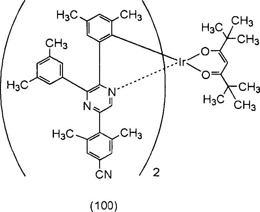
Der metallorganische Komplex, bei dem es sich um eine Ausführungsform der vorliegenden Erfindung handelt, ist aus den folgenden Gründen sehr effektiv: Der metallorganische Komplex kann eine Phosphoreszenz emittieren, d. h., er kann eine Lumineszenz von einem Triplett-Anregungszustand bereitstellen, und Licht emittieren, wodurch eine höhere Effizienz ermöglicht wird, wenn der metallorganische Komplex bei einem Licht emittierenden Element verwendet wird. Demzufolge umfasst eine Ausführungsform der vorliegenden Erfindung auch ein Licht emittierendes Element, bei dem der metallorganische Komplex einer Ausführungsform der vorliegenden Erfindung verwendet wird.The organometallic complex, which is an embodiment of the present invention, is very effective for the following reasons: The organometallic complex can emit phosphorescence, i. that is, it can provide luminescence from a triplet excited state and emit light, thereby enabling higher efficiency when the organometallic complex is used in a light-emitting element. Accordingly, an embodiment of the present invention also includes a light-emitting element using the organometallic complex of one embodiment of the present invention.

Eine weitere Ausführungsform der vorliegenden Erfindung ist ein Licht emittierendes Element, das eine EL-Schicht zwischen einem Paar von Elektroden umfasst. Die EL-Schicht umfasst eine Licht emittierende Schicht. Die Licht emittierende Schicht umfasst einen beliebigen der vorstehenden metallorganischen Komplexe. Another embodiment of the present invention is a light-emitting element comprising an EL layer between a pair of electrodes. The EL layer comprises a light-emitting layer. The light-emitting layer comprises any of the above organometallic complexes.

Eine weitere Ausführungsform der vorliegenden Erfindung ist ein Licht emittierendes Element, das eine EL-Schicht zwischen einem Paar von Elektroden umfasst. Die EL-Schicht umfasst eine Licht emittierende Schicht. Die Licht emittierende Schicht umfasst eine Vielzahl von organischen Verbindungen. Eine der Vielzahl von organischen Verbindungen ist ein beliebiger der vorstehenden metallorganischen Komplexe.Another embodiment of the present invention is a light-emitting element comprising an EL layer between a pair of electrodes. The EL layer comprises a light-emitting layer. The light-emitting layer comprises a plurality of organic compounds. One of the variety of organic compounds is any of the above organometallic complexes.

Eine Ausführungsform der vorliegenden Erfindung umfasst in ihrem Anwendungsbereich nicht nur eine Licht emittierende Vorrichtung, die das Licht emittierende Element umfasst, sondern auch eine Beleuchtungsvorrichtung, die die Licht emittierende Vorrichtung umfasst. Die Licht emittierende Vorrichtung in dieser Beschreibung bezieht sich auf eine Bildanzeigevorrichtung und eine Lichtquelle (z. B. eine Beleuchtungsvorrichtung). Außerdem umfasst die Licht emittierende Vorrichtung in ihrer Kategorie sämtliche der folgenden Module: ein Modul, bei dem ein Verbinder, wie z. B. eine flexible gedruckte Schaltung (flexible printed circuit, FPC) oder ein Tape Carrier Package (TCP), mit einer Licht emittierenden Vorrichtung verbunden ist, ein Modul, bei dem eine gedruckte Leiterplatte am Ende eines TCP bereitgestellt ist, und ein Modul, bei dem eine integrierte Schaltung (integrated circuit, IC) durch ein Chip-on-Glass-(COG-)Verfahren direkt an einem Licht emittierenden Element montiert ist.An embodiment of the present invention includes in its scope not only a light-emitting device including the light-emitting element but also a lighting device including the light-emitting device. The light-emitting device in this specification refers to an image display device and a light source (eg, a lighting device). In addition, the light-emitting device includes in its category all of the following modules: a module in which a connector, such as a connector, is used; A flexible printed circuit (FPC) or a tape carrier package (TCP) connected to a light-emitting device, a module in which a printed circuit board is provided at the end of a TCP, and a module an integrated circuit (IC) is mounted directly to a light-emitting element by a chip-on-glass (COG) method.

Entsprechend einer Ausführungsform der vorliegenden Erfindung kann ein neuartiger metallorganischer Komplex bereitgestellt werden. Entsprechend einer Ausführungsform der vorliegenden Erfindung kann ein neuartiger metallorganischer Komplex mit einer hohen Wärmebeständigkeit bereitgestellt werden. Entsprechend einer Ausführungsform der vorliegenden Erfindung kann ein neuartiger metallorganischer Komplex bereitgestellt werden, der bei einer Sublimation weniger zersetzt wird. Entsprechend einer Ausführungsform der vorliegenden Erfindung kann ein neuartiger metallorganischer Komplex mit einer hohen Farbreinheit bereitgestellt werden. Entsprechend einer Ausführungsform der vorliegenden Erfindung kann ein neuartiger metallorganischer Komplex, der bei einem Licht emittierenden Element verwendet werden kann, bereitgestellt werden. Entsprechend einer Ausführungsform der vorliegenden Erfindung kann ein neuartiger metallorganischer Komplex, der bei einer EL-Schicht eines Licht emittierenden Elements verwendet werden kann, bereitgestellt werden. Entsprechend einer Ausführungsform der vorliegenden Erfindung kann ein neuartiges Licht emittierendes Element, das einen neuartigen metallorganischen Komplex umfasst, bereitgestellt werden. Entsprechend einer Ausführungsform der vorliegenden Erfindung kann eine neuartige Licht emittierende Vorrichtung, ein neuartiges elektronisches Gerät oder eine neuartige Beleuchtungsvorrichtung bereitgestellt werden. Es sei angemerkt, dass die Beschreibung dieser Effekte dem Vorhandensein weiterer Effekte nicht im Weg steht. Eine Ausführungsform der vorliegenden Erfindung muss nicht notwendigerweise sämtliche der vorstehend aufgeführten Effekte erzielen. Weitere Effekte werden aus der Erläuterung der Beschreibung, der Zeichnungen, der Patentansprüche und dergleichen ersichtlich und können davon abgeleitet werden.According to one embodiment of the present invention, a novel organometallic complex can be provided. According to one embodiment of the present invention, a novel organometallic complex having a high heat resistance can be provided. According to one embodiment of the present invention, a novel organometallic complex can be provided which is less decomposed in a sublimation. According to one embodiment of the present invention, a novel organometallic complex having a high color purity can be provided. According to an embodiment of the present invention, a novel organometallic complex which can be used in a light-emitting element can be provided. According to one embodiment of the present invention, a novel organometallic complex which can be used in an EL layer of a light-emitting element can be provided. According to one embodiment of the present invention, a novel light-emitting element comprising a novel organometallic complex can be provided. According to an embodiment of the present invention, a novel light-emitting device, a novel electronic device or a novel lighting device can be provided. It should be noted that the description of these effects does not stand in the way of the presence of further effects. An embodiment of the present invention does not necessarily have to achieve all of the effects listed above. Other effects will be apparent from and may be deduced from the description of the specification, the drawings, the claims, and the like.

Kurze Beschreibung der ZeichnungenBrief description of the drawings

1A und 1B stellen Strukturen Licht emittierender Elemente dar. 1A and 1B represent structures of light-emitting elements.

2A und 2B stellen Strukturen Licht emittierender Elemente dar. 2A and 2 B represent structures of light-emitting elements.

3A bis 3C stellen Licht emittierende Vorrichtungen dar. 3A to 3C represent light-emitting devices.

4A und 4B stellen eine Licht emittierende Vorrichtung dar. 4A and 4B represent a light-emitting device.

5A, 5B, 5C, 5D, 5D'-1 und 5D'-2 stellen elektronische Geräte dar. 5A . 5B . 5C . 5D . 5D '1 and 5D '2 represent electronic devices.

6A bis 6C stellen ein elektronisches Gerät dar. 6A to 6C represent an electronic device.

7A und 7B stellen ein Fahrzeug dar. 7A and 7B represent a vehicle.

8A bis 8D stellen Beleuchtungsvorrichtungen dar. 8A to 8D represent lighting devices.

9 stellt Beleuchtungsvorrichtungen dar. 9 represents lighting devices.

10A und 10B stellen ein Beispiel eines Touchscreens dar. 10A and 10B represent an example of a touch screen.

11A und 11B stellen ein Beispiel eines Touchscreens dar. 11A and 11B represent an example of a touch screen.

12A und 12B stellen ein Beispiel eines Touchscreens dar. 12A and 12B represent an example of a touch screen.

13A und 13B sind ein Blockschema und ein Ablaufplan eines Berührungssensors. 13A and 13B Figure 12 is a block diagram and flow chart of a touch sensor.

14 ist ein Schaltplan eines Berührungssensors. 14 is a circuit diagram of a touch sensor.

15A, 15B1 und 15B2 stellen Blockschemata einer Anzeigevorrichtung dar. 15A . 15B1 and 15B2 represent block schemes of a display device.

16 stellt eine Schaltungskonfiguration einer Anzeigevorrichtung dar. 16 FIG. 10 illustrates a circuit configuration of a display device. FIG.

17 stellt eine Querschnittsstruktur einer Anzeigevorrichtung dar. 17 illustrates a cross-sectional structure of a display device.

18 ist ein 1H-NMR-Diagramm eines metallorganischen Komplexes, der durch die Strukturformel (100) dargestellt wird. 18 Fig. 11 is a 1 H-NMR chart of an organometallic complex represented by Structural Formula (100).

19 zeigt ein UV-VIS-Absorptionsspektrum und ein Emissionsspektrum eines metallorganischen Komplexes, der durch die Strukturformel (100) dargestellt wird. 19 Figure 11 shows a UV-visible absorption spectrum and an emission spectrum of an organometallic complex represented by Structural Formula (100).

20 zeigt LC/MS-Ergebnisse eines metallorganischen Komplexes, der durch die Strukturformel (100) dargestellt wird. 20 shows LC / MS results of an organometallic complex represented by Structural Formula (100).

21 zeigt die Beziehung zwischen einem Partialdruck, der durch ein Quadrupol-Massenspektrometer erhalten wurde, und einem Masse-zu-Ladungs-Verhältnis. 21 Fig. 14 shows the relationship between a partial pressure obtained by a quadrupole mass spectrometer and a mass-to-charge ratio.

22 zeigt thermogravimetrische Kurven von metallorganischen Komplexen. 22 shows thermogravimetric curves of organometallic complexes.

23 stellt ein Licht emittierendes Element dar. 23 represents a light-emitting element.

24 zeigt Stromdichte-Leuchtdichte-Eigenschaften eines Licht emittierenden Elements 1, eines Licht emittierenden Elements 2 und eines Licht emittierenden Vergleichselements 3. 24 shows current density-luminance characteristics of a light-emitting element 1, a light-emitting element 2, and a comparative light-emitting element 3.

25 zeigt Spannungs–Leuchtdichte-Eigenschaften eines Licht emittierenden Elements 1, eines Licht emittierenden Elements 2 und eines Licht emittierenden Vergleichselements 3. 25 FIG. 12 shows voltage-luminance characteristics of a light-emitting element 1, a light-emitting element 2, and a comparative light-emitting element 3.

26 zeigt Leuchtdichte-Stromeffizienz-Eigenschaften eines Licht emittierenden Elements 1, eines Licht emittierenden Elements 2 und eines Licht emittierenden Vergleichselements 3. 26 FIG. 12 shows luminance-current efficiency characteristics of a light-emitting element 1, a light-emitting element 2 and a comparative light-emitting element 3.

27 zeigt Spannungs–Strom-Eigenschaften eines Licht emittierenden Elements 1, eines Licht emittierenden Elements 2 und eines Licht emittierenden Vergleichselements 3. 27 shows voltage-current characteristics of a light-emitting element 1, a light-emitting element 2 and a comparative light-emitting element 3.

28 zeigt CIE-Chromatizitätsdiagramme eines Licht emittierenden Elements 1, eines Licht emittierenden Elements 2 und eines Licht emittierenden Vergleichselements 3. 28 shows CIE chromaticity diagrams of a light-emitting element 1, a light-emitting element 2 and a comparative light-emitting element 3.

29 zeigt Emissionsspektren eines Licht emittierenden Elements 1, eines Licht emittierenden Elements 2 und eines Licht emittierenden Vergleichselements 3. 29 FIG. 12 shows emission spectra of a light-emitting element 1, a light-emitting element 2, and a comparative light-emitting element 3.

30 zeigt die Zuverlässigkeit eines Licht emittierenden Elements 1, eines Licht emittierenden Elements 2 und eines Licht emittierenden Vergleichselements 3. 30 shows the reliability of a light-emitting element 1, a light-emitting element 2 and a comparative light-emitting element 3.

31A und 31B stellen ein Licht emittierendes Element dar. 31A and 31B represent a light-emitting element.

32 zeigt ein 1H-NMR-Diagramm eines metallorganischen Komplexes, der durch die Strukturformel (108) dargestellt wird. 32 Fig. 11 is a 1 H-NMR chart of an organometallic complex represented by Structural Formula (108).

33 zeigt ein UV-VIS-Absorptionsspektrum und ein Emissionsspektrum eines metallorganischen Komplexes, der durch die Strukturformel (108) dargestellt wird. 33 Fig. 12 shows a UV-VIS absorption spectrum and an emission spectrum of an organometallic complex represented by Structural Formula (108).

34 ist ein 1H-NMR-Diagramm eines metallorganischen Komplexes, der durch die Strukturformel (114) dargestellt wird. 34 Fig. 11 is a 1 H-NMR chart of an organometallic complex represented by Structural Formula (114).

35 zeigt ein UV-VIS-Absorptionsspektrum und ein Emissionsspektrum eines metallorganischen Komplexes, der durch die Strukturformel (114) dargestellt wird. 35 Figure 4 shows a UV-visible absorption spectrum and an emission spectrum of an organometallic complex represented by Structural Formula (114).

36 zeigt Stromdichte-Leuchtdichte-Eigenschaften eines Licht emittierenden Elements 4, eines Licht emittierenden Elements 5 und eines Licht emittierenden Vergleichselements 6. 36 FIG. 12 shows current density-luminance characteristics of a light-emitting element 4, a light-emitting element 5, and a comparative light-emitting element 6.

37 zeigt Spannungs-Leuchtdichte-Eigenschaften eines Licht emittierenden Elements 4, eines Licht emittierenden Elements 5 und eines Licht emittierenden Vergleichselements 6. 37 FIG. 10 shows voltage-luminance characteristics of a light-emitting element 4, a light-emitting element 5, and a comparative light-emitting element 6.

38 zeigt Leuchtdichte-Stromeffizienz-Eigenschaften eines Licht emittierenden Elements 4, eines Licht emittierenden Elements 5 und eines Licht emittierenden Vergleichselements 6. 38 FIG. 10 shows luminance-current efficiency characteristics of a light-emitting element 4, a light-emitting element 5, and a comparative light-emitting element 6.

39 zeigt Spannungs-Strom-Eigenschaften eines Licht emittierenden Elements 4, eines Licht emittierenden Elements 5 und eines Licht emittierenden Vergleichselements 6. 39 shows voltage-current characteristics of a light-emitting element 4, a light-emitting element 5 and a comparative light-emitting element 6.

40 zeigt CIE-Chromatizitätsdiagramme eines Licht emittierenden Elements 4, eines Licht emittierenden Elements 5 und eines Licht emittierenden Vergleichselements 6. 40 Fig. 12 shows CIE chromaticity diagrams of a light-emitting element 4, a light-emitting element 5 and a comparative light-emitting element 6.

41 zeigt Emissionsspektren eines Licht emittierenden Elements 4 und eines Licht emittierenden Elements 5. 41 shows emission spectra of a light-emitting element 4 and a light-emitting element 5.

42 zeigt die Zuverlässigkeit eines Licht emittierenden Elements 4, eines Licht emittierenden Elements 5 und eines Licht emittierenden Vergleichselements 6. 42 shows the reliability of a light-emitting element 4, a light-emitting element 5 and a comparative light-emitting element 6.

Detaillierte Beschreibung der ErfindungDetailed description of the invention

Ausführungsformen der vorliegenden Erfindung werden nachstehend anhand der Zeichnungen beschrieben. Die vorliegende Erfindung ist jedoch nicht auf die folgende Beschreibung beschränkt, und die Modi und die Details können auf verschiedene Art und Weise verändert werden, soweit sie nicht vom Schutzbereich und Wesen der vorliegenden Erfindung abweichen. Dementsprechend sollte die vorliegende Erfindung nicht als auf die Beschreibung der folgenden Ausführungsformen und Beispiele beschränkt angesehen werden.Embodiments of the present invention will be described below with reference to the drawings. However, the present invention is not limited to the following description, and the modes and the details may be changed in various ways as far as they do not depart from the scope and spirit of the present invention. Accordingly, the present invention should not be construed as being limited to the description of the following embodiments and examples.

Es sei angemerkt, dass die Begriffe „Film” und „Schicht” je nach Sachlage oder Umständen miteinander ausgetauscht werden können. Beispielsweise kann in einigen Fällen der Begriff „leitende Schicht” durch den Begriff „leitender Film” ersetzt werden. Der Begriff „isolierender Film” kann auch in einigen Fällen durch den Begriff „isolierende Schicht” ersetzt werden.It should be noted that the terms "film" and "layer" may be interchanged depending on the circumstances or circumstances. For example, in some instances, the term "conductive layer" may be replaced by the term "conductive film". The term "insulating film" may also be replaced by the term "insulating layer" in some cases.

(Ausführungsform 1)(Embodiment 1)

Bei dieser Ausführungsform werden metallorganische Komplexe, bei denen es sich jeweils um eine Ausführungsform der vorliegenden Erfindung handelt, beschrieben.In this embodiment, organometallic complexes which are each an embodiment of the present invention will be described.

Der metallorganische Komplex, der bei dieser Ausführungsform beschrieben wird, umfasst Iridium als Zentralmetall und einen Liganden. Der Ligand weist ein Pyrazin-Gerüst auf. Iridium ist an Stickstoff an der 1-Position des Pyrazin-Gerüsts gebunden. Eine Phenyl-Gruppe ist jeweils an die 2-, 3- und 5-Position des Pyrazin-Gerüsts gebunden. Die Phenyl-Gruppen, die an die 2- und 3-Position gebunden sind, weisen jeweils eine Alkyl-Gruppe als Substituenten auf. Die Phenyl-Gruppe, die an die 5-Position gebunden ist, weist eine Cyano-Gruppe als Substituenten auf.The organometallic complex described in this embodiment includes iridium as a central metal and a ligand. The ligand has a pyrazine skeleton. Iridium is bound to nitrogen at the 1-position of the pyrazine backbone. Each phenyl group is attached to the 2-, 3- and 5-position of the pyrazine skeleton. The phenyl groups attached to the 2- and 3-positions each have an alkyl group as a substituent. The phenyl group attached to the 5-position has a cyano group as a substituent.

Der metallorganische Komplex, der bei dieser Ausführungsform beschrieben wird, umfasst einen ersten Liganden und einen zweiten Liganden, die an Iridium als Zentralmetall gebunden ist. Der erste Ligand weist ein Pyrazin-Gerüst auf. Iridium ist an Stickstoff an der 1-Position des Pyrazin-Gerüsts gebunden. Eine Phenyl-Gruppe ist jeweils an die 2-, 3- und 5-Position des Pyrazin-Gerüsts gebunden. Die Phenyl-Gruppen, die an die 2- und 3-Position gebunden sind, weisen jeweils eine Alkyl-Gruppe als Substituenten auf. Die Phenyl-Gruppe, die an die 5-Position gebunden ist, weist eine Cyano-Gruppe als Substituenten auf. Der zweite Ligand ist ein monoanionischer Ligand. Insbesondere handelt es sich bei dem zweiten Liganden in dem metallorganischen Komplex um einen monoanionischen zweizähnigen Chelat-Liganden mit einer β-Diketon-Struktur, einen monoanionischen zweizähnigen Chelat-Liganden mit einer Carboxyl-Gruppe, einen monoanionischen zweizähnigen Chelat-Liganden mit einer phenolischen Hydroxyl-Gruppe, einen monoanionischen zweizähnigen Chelat-Liganden, bei dem zwei koordinierte Elemente jeweils Stickstoff sind, oder einen aromatischen heterocyclischen zweizähnigen Liganden, der durch Cyclometallierung eine Metall-Kohlenstoff-Bindung mit Iridium bilden kann.The organometallic complex described in this embodiment comprises a first ligand and a second ligand bound to iridium as the central metal. The first ligand has a pyrazine backbone. Iridium is bound to nitrogen at the 1-position of the pyrazine backbone. Each phenyl group is attached to the 2-, 3- and 5-position of the pyrazine skeleton. The phenyl groups attached to the 2- and 3-positions each have an alkyl group as a substituent. The phenyl group attached to the 5-position has a cyano group as a substituent. The second ligand is a monoanionic ligand. In particular, the second ligand in the organometallic complex is a monoanionic bidentate chelate ligand having a β-diketone structure, a monoanionic bidentate chelate ligand having a carboxyl group, a monoanionic bidentate chelate ligand having a phenolic hydroxyl group. Group, a monoanionic bidentate chelate ligand in which two coordinated elements are each nitrogen, or an aromatic heterocyclic bidentate ligand, which can form a metal-carbon bond with iridium by cyclometalation.

Bei dem vorstehend beschriebenen metallorganischen Komplex einer Ausführungsform der vorliegenden Erfindung ist die Phenyl-Gruppe, die die Alkyl-Gruppe als Substituenten aufweist, jeweils an die 2- und 3-Position des Pyrazin-Gerüsts gebunden, das in dem Liganden enthalten ist, und die Phenyl-Gruppe, die die Cyano-Gruppe als Substituenten aufweist, ist an die 5-Position des Pyrazin-Gerüsts gebunden. Die ortho-Position der Phenyl-Gruppe, die an die 2-Position des Pyrazin-Gerüsts gebunden ist, ist an Iridium gebunden. In the above-described organometallic complex of an embodiment of the present invention, the phenyl group having the alkyl group as a substituent is bonded respectively to the 2 and 3 positions of the pyrazine skeleton contained in the ligand and Phenyl group having the cyano group as a substituent is bonded to the 5-position of the pyrazine skeleton. The ortho position of the phenyl group attached to the 2-position of the pyrazine backbone is bound to iridium.

In dem metallorganischen Komplex einer Ausführungsform der vorliegenden Erfindung weisen die Phenyl-Gruppen, die an die 2- und 3-Position des Pyrazin-Gerüsts gebunden sind, jeweils eine Alkyl-Gruppe als Substituenten auf; demzufolge kann die Karbonisierung infolge einer Reaktion zwischen den metallorganischen Komplexen bei der Sublimation verhindert werden, und die Sublimationstemperatur kann verringert werden. Jedoch haben die Erfinder der vorliegenden Erfindung andererseits herausgefunden, dass die Alkyl-Gruppe mit derartigen Effekten eine geringe Menge an einem Abbauprodukt mit einem niedrigen Molekulargewicht bei der Sublimation erzeugt, was die Lebensdauer eines Licht emittierenden Elements verringert. Außerdem haben die Erfinder der vorliegenden Erfindung herausgefunden, dass in dem Fall, in dem die Phenyl-Gruppe, die an die 5-Position des Pyrazin-Gerüsts gebunden ist, die Cyano-Gruppe als Substituenten aufweist, eine Behandlung mit einer hohen Temperatur bei der Sublimation nicht zu der Entstehung eines Abbauprodukts mit einem niedrigen Molekulargewicht auf Grund der Alkyl-Gruppe und dem daraus folgenden Freisetzen eines Gases führt, obwohl die Sublimationstemperatur höher als diejenige in dem Fall ist, in dem die Cyano-Gruppe nicht enthalten ist.In the organometallic complex of one embodiment of the present invention, the phenyl groups bonded to the 2 and 3 positions of the pyrazine skeleton each have an alkyl group as a substituent; consequently, the carbonization due to a reaction between the organometallic complexes in the sublimation can be prevented, and the sublimation temperature can be lowered. On the other hand, the inventors of the present invention have found, on the other hand, that the alkyl group having such effects produces a small amount of a low molecular weight decomposition product in sublimation, which reduces the life of a light-emitting element. In addition, the inventors of the present invention have found that, in the case where the phenyl group bonded to the 5-position of the pyrazine skeleton has the cyano group as a substituent, a high-temperature treatment in the Sublimation does not result in the formation of a low molecular weight degradation product due to the alkyl group and the consequent release of a gas, although the sublimation temperature is higher than that in the case where the cyano group is not contained.

Demzufolge ist ein Merkmal des metallorganischen Komplexes einer Ausführungsform der vorliegenden Erfindung, dass die Phenyl-Gruppen, die an die 2- und 3-Position des Pyrazin-Gerüsts gebunden sind, jeweils die Alkyl-Gruppe als Substituenten aufweisen und dass die Phenyl-Gruppe, die an die 5-Position des Pyrazin-Gerüsts gebunden ist, die Cyano-Gruppe als Substituenten aufweist. Es sei angemerkt, dass der metallorganische Komplex einer Ausführungsform der vorliegenden Erfindung nach der Sublimationsreinigung nicht leicht Strukturisomere erzeugt, die als Verunreinigungen die Elementeigenschaften beeinträchtigen können. Folglich kann, wenn der metallorganische Komplex bei der Herstellung eines Elements durch Vakuumverdampfung verwendet wird, ein Beimischen eines Abbauprodukts zu dem Element verhindert werden, und somit kann das Element vorteilhafte Lebensdauer-Eigenschaften aufweisen.Accordingly, a feature of the organometallic complex of one embodiment of the present invention is that the phenyl groups attached to the 2- and 3-positions of the pyrazine skeleton each have the alkyl group as a substituent and that the phenyl group, which is bonded to the 5-position of the pyrazine skeleton having cyano group as a substituent. It should be noted that the organometallic complex of one embodiment of the present invention, after sublimation cleaning, does not readily produce structural isomers which, as impurities, may affect the elemental properties. Consequently, when the organometallic complex is used in the production of an element by vacuum evaporation, mixing of a decomposition product to the element can be prevented, and thus the element can have favorable life characteristics.

Wenn die Phenyl-Gruppen, die an die 2- und 3-Position des Pyrazin-Gerüsts gebunden sind, keine Alkyl-Gruppe als Substituenten aufweisen, tritt eine Karbonisierung infolge einer Reaktion zwischen den metallorganischen Komplexen selbst dann bei der Sublimation auf, wenn die Phenyl-Gruppe, die an die 5-Position des Pyrazin-Gerüsts gebunden ist, eine Cyano-Gruppe aufweist. Demzufolge muss der metallorganische Komplex einer Ausführungsform der vorliegenden Erfindung sowohl die Alkyl-Gruppe als auch die Cyano-Gruppe aufweisen, um die Karbonisierung infolge einer Reaktion zwischen den metallorganischen Komplexen und das Freisetzen eines Gases mit einem niedrigen Molekulargewicht zu verhindern, was eine neue Entdeckung ist.When the phenyl groups attached to the 2 and 3 positions of the pyrazine skeleton do not have an alkyl group as a substituent, carbonation due to a reaction between the organometallic complexes occurs in the sublimation even if the phenyl Group attached to the 5-position of the pyrazine skeleton has a cyano group. Accordingly, the organometallic complex of one embodiment of the present invention must have both the alkyl group and the cyano group to prevent carbonization due to a reaction between the organometallic complexes and the release of a low molecular weight gas, which is a new discovery ,

Des Weiteren weist die Cyano-Gruppe, die in dem metallorganischen Komplex einer Ausführungsform der vorliegenden Erfindung enthalten ist, einen Effekt zum Verschieben des Emissionsspektrums des metallorganischen Komplexes zu einer langen Wellenlängenseite auf. Mit anderen Worten: Der metallorganische Komplex einer Ausführungsform der vorliegenden Erfindung emittiert ein tiefrotes Licht mit einer hohen Farbreinheit. Tiefrote Lichtemission weist im Allgemeinen ein Spektrum auf, das den Nahinfrarotbereich abdeckt, und somit weist sie einen niedrigen Leuchtstärkefaktor auf; jedoch kann eine Verringerung des Leuchtstärkefaktors minimiert werden, da die Alkyl-Gruppe in dem metallorganischen Komplex einer Ausführungsform der vorliegenden Erfindung (die Alkyl-Gruppen, die in den Phenyl-Gruppen enthalten sind, die an die 2- und 3-Position des Pyrazin-Gerüsts gebunden sind) auch einen Effekt zum Verschmälern eines Emissionsspektrums aufweist. Demzufolge kann tiefrotes Licht, das von dem metallorganischen Komplex einer Ausführungsform der vorliegenden Erfindung emittiert wird, sowohl eine hohe Farbreinheit als auch eine hohe Effizienz erzielen.Further, the cyano group contained in the organometallic complex of one embodiment of the present invention has an effect of shifting the emission spectrum of the organometallic complex to a long wavelength side. In other words, the organometallic complex of one embodiment of the present invention emits a deep red light having a high color purity. Deep red light emission generally has a spectrum covering the near infrared region, and thus has a low luminance factor; however, a reduction in the luminance factor can be minimized because the alkyl group in the organometallic complex of one embodiment of the present invention (the alkyl groups contained in the phenyl groups attached to the 2 and 3 positions of the pyrazine nucleus) Skeleton are bound) also has an effect of narrowing an emission spectrum. As a result, deep red light emitted from the organometallic complex of one embodiment of the present invention can achieve both high color purity and high efficiency.

Es sei angemerkt, dass bei der vorstehenden Struktur die Phenyl-Gruppe, die an die 5-Position des Pyrazin-Gerüsts gebunden ist, vorzugsweise ferner nicht nur eine Cyano-Gruppe, sondern auch eine Alkyl-Gruppe aufweist, um die Karbonisierung infolge einer Reaktion zwischen den metallorganischen Komplexen zu verhindern. Insbesondere kann eine Alkyl-Gruppe, die an die 2-Position der Phenyl-Gruppe gebunden ist, die an die 5-Position des Pyrazin-Gerüsts gebunden ist, verhindern, dass ein Peak eines Emissionsspektrums bei einer zu langen Wellenlänge auftritt, und kann einen Leuchtstärkefaktor aufrechterhalten. Das heißt: Diese Struktur ist insbesondere dafür geeignet, eine hohe Farbreinheit und eine tiefrote Emission mit hoher Effizienz zu erzielen.It should be noted that in the above structure, the phenyl group bonded to the 5-position of the pyrazine skeleton preferably further has not only a cyano group but also an alkyl group to prevent carbonization due to a reaction between the organometallic complexes. In particular, an alkyl group attached to the 2-position of the phenyl group bonded to the 5-position of the pyrazine skeleton can prevent a peak of an emission spectrum from occurring at too long a wavelength, and can be one Maintained luminous intensity factor. That is, this structure is particularly suitable for achieving high color purity and deep red emission with high efficiency.

Ein metallorganischer Komplex, der bei dieser Ausführungsform beschrieben wird, wird durch die folgende allgemeine Formel (G1) dargestellt.

Figure DE102016225271A1_0013
An organometallic complex described in this embodiment is represented by the following general formula (G1).
Figure DE102016225271A1_0013

Es sei angemerkt, dass in der allgemeinen Formel (G1) A1 bis A4 jeweils unabhängig voneinander eine substituierte oder nicht substituierte Alkyl-Gruppe mit 1 bis 6 Kohlenstoffatomen darstellen. R1 bis R6 stellen jeweils unabhängig voneinander Wasserstoff, eine substituierte oder nicht substituierte Alkyl-Gruppe mit 1 bis 6 Kohlenstoffatomen, eine substituierte oder nicht substituierte Aryl-Gruppe mit 6 bis 13 Kohlenstoffatomen oder eine substituierte oder nicht substituierte Heteroaryl-Gruppe mit 3 bis 12 Kohlenstoffatomen dar. R7 bis R11 stellen jeweils unabhängig voneinander Wasserstoff, eine substituierte oder nicht substituierte Alkyl-Gruppe mit 1 bis 6 Kohlenstoffatomen, eine substituierte oder nicht substituierte Aryl-Gruppe mit 6 bis 13 Kohlenstoffatomen, eine substituierte oder nicht substituierte Heteroaryl-Gruppe mit 3 bis 12 Kohlenstoffatomen, oder eine Cyano-Gruppe dar. Mindestens eines von R7 bis R11 stellt eine Cyano-Gruppe dar.It should be noted that in the general formula (G1), A 1 to A 4 each independently represent a substituted or unsubstituted alkyl group having 1 to 6 carbon atoms. R 1 to R 6 each independently represent hydrogen, a substituted or unsubstituted alkyl group of 1 to 6 carbon atoms, a substituted or unsubstituted aryl group of 6 to 13 carbon atoms or a substituted or unsubstituted heteroaryl group of 3 to R 7 to R 11 each independently represent hydrogen, a substituted or unsubstituted alkyl group of 1 to 6 carbon atoms, a substituted or unsubstituted aryl group of 6 to 13 carbon atoms, a substituted or unsubstituted heteroaryl group; At least one of R 7 to R 11 represents a cyano group.

Ein metallorganischer Komplex, der bei dieser Ausführungsform beschrieben wird, wird durch die folgende allgemeine Formel (G2) dargestellt.

Figure DE102016225271A1_0014
An organometallic complex described in this embodiment is represented by the following general formula (G2).
Figure DE102016225271A1_0014

Es sei angemerkt, dass in der allgemeinen Formel (G2) A1 bis A4 jeweils unabhängig voneinander eine substituierte oder nicht substituierte Alkyl-Gruppe mit 1 bis 6 Kohlenstoffatomen darstellen. R6 stellt Wasserstoff, eine substituierte oder nicht substituierte Alkyl-Gruppe mit 1 bis 6 Kohlenstoffatomen, eine substituierte oder nicht substituierte Aryl-Gruppe mit 6 bis 13 Kohlenstoffatomen oder eine substituierte oder nicht substituierte Heteroaryl-Gruppe mit 3 bis 12 Kohlenstoffatomen dar. R7 bis R11 stellen jeweils unabhängig voneinander Wasserstoff, eine substituierte oder nicht substituierte Alkyl-Gruppe mit 1 bis 6 Kohlenstoffatomen, eine substituierte oder nicht substituierte Aryl-Gruppe mit 6 bis 13 Kohlenstoffatomen, eine substituierte oder nicht substituierte Heteroaryl-Gruppe mit 3 bis 12 Kohlenstoffatomen oder eine Cyano-Gruppe dar. Mindestens eines von R7 bis R11 stellt eine Cyano-Gruppe dar.It should be noted that in the general formula (G2), A 1 to A 4 each independently represent a substituted or unsubstituted alkyl group having 1 to 6 carbon atoms. R 6 represents hydrogen, a substituted or unsubstituted alkyl group having 1 to 6 carbon atoms, a substituted or unsubstituted aryl group having 6 to 13 carbon atoms or a substituted or unsubstituted heteroaryl group having 3 to 12 carbon atoms. R 7 to R 11 each independently represent hydrogen, a substituted or unsubstituted alkyl group having 1 to 6 carbon atoms, a substituted or unsubstituted aryl group having 6 to 13 carbon atoms, a substituted or unsubstituted heteroaryl group having 3 to 12 carbon atoms or a cyano group. At least one of R 7 to R 11 represents a cyano group.

Ein metallorganischer Komplex, der bei dieser Ausführungsform beschrieben wird, wird durch die folgende allgemeine Formel (G3) dargestellt.

Figure DE102016225271A1_0015
An organometallic complex described in this embodiment is represented by the following general formula (G3).
Figure DE102016225271A1_0015

Es sei angemerkt, dass in der allgemeinen Formel (G3) A1 bis A4 jeweils unabhängig voneinander eine substituierte oder nicht substituierte Alkyl-Gruppe mit 1 bis 6 Kohlenstoffatomen darstellen. R1 bis R6 stellen jeweils unabhängig voneinander Wasserstoff, eine substituierte oder nicht substituierte Alkyl-Gruppe mit 1 bis 6 Kohlenstoffatomen, eine substituierte oder nicht substituierte Aryl-Gruppe mit 6 bis 13 Kohlenstoffatomen oder eine substituierte oder nicht substituierte Heteroaryl-Gruppe mit 3 bis 12 Kohlenstoffatomen dar. R7 bis R11 stellen jeweils unabhängig voneinander Wasserstoff, eine substituierte oder nicht substituierte Alkyl-Gruppe mit 1 bis 6 Kohlenstoffatomen, eine substituierte oder nicht substituierte Aryl-Gruppe mit 6 bis 13 Kohlenstoffatomen, eine substituierte oder nicht substituierte Heteroaryl-Gruppe mit 3 bis 12 Kohlenstoffatomen oder eine Cyano-Gruppe dar. Mindestens eines von R7 bis R11 stellt eine Cyano-Gruppe dar. L stellt einen monoanionischen Liganden dar. Ein metallorganischer Komplex, der bei dieser Ausführungsform beschrieben wird, wird durch die folgende allgemeine Formel (G4) dargestellt.

Figure DE102016225271A1_0016
It should be noted that in the general formula (G3), A 1 to A 4 each independently represent a substituted or unsubstituted alkyl group having 1 to 6 carbon atoms. R 1 to R 6 each independently represent hydrogen, a substituted or unsubstituted alkyl group of 1 to 6 carbon atoms, a substituted or unsubstituted aryl group of 6 to 13 carbon atoms or a substituted or unsubstituted heteroaryl group of 3 to R 7 to R 11 each independently represent hydrogen, a substituted or unsubstituted alkyl group of 1 to 6 carbon atoms, a substituted or unsubstituted aryl group of 6 to 13 carbon atoms, a substituted or unsubstituted heteroaryl group; At least one of R 7 to R 11 represents a cyano group. L represents a monoanionic ligand. An organometallic complex described in this embodiment is exemplified by the following general formula (G4).
Figure DE102016225271A1_0016

Es sei angemerkt, dass in der allgemeinen Formel (G4) A1 bis A4 jeweils unabhängig voneinander eine substituierte oder nicht substituierte Alkyl-Gruppe mit 1 bis 6 Kohlenstoffatomen darstellen. R6 stellt Wasserstoff, eine substituierte oder nicht substituierte Alkyl-Gruppe mit 1 bis 6 Kohlenstoffatomen, eine substituierte oder nicht substituierte Aryl-Gruppe mit 6 bis 13 Kohlenstoffatomen oder eine substituierte oder nicht substituierte Heteroaryl-Gruppe mit 3 bis 12 Kohlenstoffatomen dar. R7 bis R11 stellen jeweils unabhängig voneinander Wasserstoff, eine substituierte oder nicht substituierte Alkyl-Gruppe mit 1 bis 6 Kohlenstoffatomen, eine substituierte oder nicht substituierte Aryl-Gruppe mit 6 bis 13 Kohlenstoffatomen, eine substituierte oder nicht substituierte Heteroaryl-Gruppe mit 3 bis 12 Kohlenstoffatomen oder eine Cyano-Gruppe dar. Mindestens eines von R7 bis R11 stellt eine Cyano-Gruppe dar. L stellt einen monoanionischen Liganden dar.It should be noted that in the general formula (G4), A 1 to A 4 each independently represent a substituted or unsubstituted alkyl group having 1 to 6 carbon atoms. R 6 represents hydrogen, a substituted or unsubstituted alkyl group having 1 to 6 carbon atoms, a substituted or unsubstituted aryl group having 6 to 13 carbon atoms or a substituted or unsubstituted heteroaryl group having 3 to 12 carbon atoms. R 7 to R 11 each independently represent hydrogen, a substituted or unsubstituted alkyl group having 1 to 6 carbon atoms, a substituted or unsubstituted aryl group having 6 to 13 carbon atoms, a substituted or unsubstituted heteroaryl group having 3 to 12 carbon atoms or a cyano group. At least one of R 7 to R 11 represents a cyano group. L represents a monoanionic ligand.

Bei den vorstehenden Strukturen umfassen Beispiele für den monoanionischen Liganden einen monoanionischen zweizähnigen Chelat-Liganden mit einer β-Diketon-Struktur, einen monoanionischen zweizähnigen Chelat-Liganden mit einer Carboxyl-Gruppe, einen monoanionischen zweizähnigen Chelat-Liganden mit einer phenolischen Hydroxyl-Gruppe, einen monoanionischen zweizähnigen Chelat-Liganden, bei dem zwei koordinierte Elemente jeweils Stickstoff sind, oder einen aromatischen heterocyclischen zweizähnigen Liganden, der durch Cyclometallierung eine Metall-Kohlenstoff-Bindung mit Iridium bilden kann.In the above structures, examples of the monoanionic ligand include a monoanionic bidentate chelate ligand having a β-diketone structure, a monoanionic bidentate chelate ligand having a carboxyl group, a monoanionic bidentate chelating ligand having a phenolic hydroxyl group, a monoanionic bidentate chelate ligands, in which two coordinated elements are each nitrogen, or an aromatic heterocyclic bidentate ligand, which can form a metal-carbon bond with iridium by cyclometalation.

Der monoanionische Ligand wird durch eine der folgenden allgemeinen Formeln (L1) bis (L6) dargestellt.

Figure DE102016225271A1_0017
The monoanionic ligand is represented by one of the following general formulas (L1) to (L6).
Figure DE102016225271A1_0017

In den allgemeinen Formeln (L1) bis (L6) stellen R71 bis R94 jeweils unabhängig voneinander Wasserstoff, eine substituierte oder nicht substituierte Alkyl-Gruppe mit 1 bis 6 Kohlenstoffatomen, eine Halogen-Gruppe, eine Vinyl-Gruppe, eine substituierte oder nicht substituierte Haloalkyl-Gruppe mit 1 bis 6 Kohlenstoffatomen, eine substituierte oder nicht substituierte Alkoxy-Gruppe mit 1 bis 6 Kohlenstoffatomen oder eine substituierte oder nicht substituierte Alkylthio-Gruppe mit 1 bis 6 Kohlenstoffatomen dar. A1 bis A3 stellen jeweils unabhängig voneinander Stickstoff, sp2-hybridisierten Kohlenstoff, der an Wasserstoff gebunden ist, oder sp2-hybridisierten Kohlenstoff mit einem Substituenten dar. Der Substituent ist eine Alkyl-Gruppe mit 1 bis 6 Kohlenstoffatomen, eine Halogen-Gruppe, eine Haloalkyl-Gruppe mit 1 bis 6 Kohlenstoffatomen oder eine Phenyl-Gruppe. B1 bis B8 stellen jeweils unabhängig voneinander Stickstoff oder substituierten oder nicht substituierten Kohlenstoff dar. Der Substituent ist eine Alkyl-Gruppe mit 1 bis 6 Kohlenstoffatomen, eine Halogen-Gruppe, eine Haloalkyl-Gruppe mit 1 bis 6 Kohlenstoffatomen oder eine Phenyl-Gruppe.In the general formulas (L1) to (L6), R 71 to R 94 each independently represent hydrogen, a substituted or unsubstituted alkyl group having 1 to 6 carbon atoms, a halogen group, a vinyl group, a substituted or not substituted haloalkyl group having 1 to 6 carbon atoms, a substituted or unsubstituted alkoxy group having 1 to 6 carbon atoms or a substituted or unsubstituted alkylthio group having 1 to 6 carbon atoms. A 1 to A 3 each independently represent nitrogen, sp 2 -hybridized carbon which is bonded to hydrogen, or sp 2 -hybridized carbon with a substituent. the substituent is an alkyl group having 1 to 6 carbon atoms, a halogen group, a haloalkyl group having 1 to 6 carbon atoms, or a phenyl group. Each of B 1 to B 8 independently represents nitrogen or substituted or unsubstituted carbon. The substituent is an alkyl group having 1 to 6 carbon atoms, a halogen group, a haloalkyl group having 1 to 6 carbon atoms, or a phenyl group ,

Ein metallorganischer Komplex, der bei dieser Ausführungsform beschrieben wird, wird durch die folgende allgemeine Formel (G5) dargestellt.

Figure DE102016225271A1_0018
An organometallic complex described in this embodiment is represented by the following general formula (G5).
Figure DE102016225271A1_0018

Es sei angemerkt, dass in der allgemeinen Formel (G5) A1 bis A4 jeweils unabhängig voneinander eine substituierte oder nicht substituierte Alkyl-Gruppe mit 1 bis 6 Kohlenstoffatomen darstellen. R1 bis R6 stellen jeweils unabhängig voneinander Wasserstoff, eine substituierte oder nicht substituierte Alkyl-Gruppe mit 1 bis 6 Kohlenstoffatomen, eine substituierte oder nicht substituierte Aryl-Gruppe mit 6 bis 13 Kohlenstoffatomen oder eine substituierte oder nicht substituierte Heteroaryl-Gruppe mit 3 bis 12 Kohlenstoffatomen dar. R7 bis R11 stellen jeweils unabhängig voneinander Wasserstoff, eine substituierte oder nicht substituierte Alkyl-Gruppe mit 1 bis 6 Kohlenstoffatomen, eine substituierte oder nicht substituierte Aryl-Gruppe mit 6 bis 13 Kohlenstoffatomen, eine substituierte oder nicht substituierte Heteroaryl-Gruppe mit 3 bis 12 Kohlenstoffatomen oder eine Cyano-Gruppe dar. Mindestens eines von R7 bis R11 stellt eine Cyano-Gruppe dar.It should be noted that in the general formula (G5), A 1 to A 4 each independently represent a substituted or unsubstituted alkyl group having 1 to 6 carbon atoms. R 1 to R 6 each independently represent hydrogen, a substituted or unsubstituted alkyl group of 1 to 6 carbon atoms, a substituted or unsubstituted aryl group of 6 to 13 carbon atoms or a substituted or unsubstituted heteroaryl group of 3 to R 7 to R 11 each independently represent hydrogen, a substituted or unsubstituted alkyl group of 1 to 6 carbon atoms, a substituted or unsubstituted aryl group of 6 to 13 carbon atoms, a substituted or unsubstituted heteroaryl group; At least one of R 7 to R 11 represents a cyano group.

Ein metallorganischer Komplex, der bei dieser Ausführungsform beschrieben wird, wird durch die folgende allgemeine Formel (G6) dargestellt.

Figure DE102016225271A1_0019
An organometallic complex described in this embodiment is represented by the following general formula (G6).
Figure DE102016225271A1_0019

Es sei angemerkt, dass in der allgemeinen Formel (G6) A1 bis A4 jeweils unabhängig voneinander eine substituierte oder nicht substituierte Alkyl-Gruppe mit 1 bis 6 Kohlenstoffatomen darstellen. R6 stellt Wasserstoff, eine substituierte oder nicht substituierte Alkyl-Gruppe mit 1 bis 6 Kohlenstoffatomen, eine substituierte oder nicht substituierte Aryl-Gruppe mit 6 bis 13 Kohlenstoffatomen oder eine substituierte oder nicht substituierte Heteroaryl-Gruppe mit 3 bis 12 Kohlenstoffatomen dar. R7 bis R11 stellen jeweils unabhängig voneinander Wasserstoff, eine substituierte oder nicht substituierte Alkyl-Gruppe mit 1 bis 6 Kohlenstoffatomen, eine substituierte oder nicht substituierte Aryl-Gruppe mit 6 bis 13 Kohlenstoffatomen, eine substituierte oder nicht substituierte Heteroaryl-Gruppe mit 3 bis 12 Kohlenstoffatomen oder eine Cyano-Gruppe dar. Mindestens eines von R7 bis R11 stellt eine Cyano-Gruppe dar.It should be noted that in the general formula (G6), A 1 to A 4 each independently represent a substituted or unsubstituted alkyl group having 1 to 6 carbon atoms. R 6 represents hydrogen, a substituted or unsubstituted alkyl group having 1 to 6 carbon atoms, a substituted or unsubstituted aryl group having 6 to 13 carbon atoms or a substituted or unsubstituted heteroaryl group having 3 to 12 carbon atoms. R 7 to R 11 each independently represent hydrogen, a substituted or unsubstituted alkyl group having 1 to 6 carbon atoms, a substituted or unsubstituted aryl group having 6 to 13 carbon atoms, a substituted or unsubstituted heteroaryl group having 3 to 12 carbon atoms or a cyano group. At least one of R 7 to R 11 represents a cyano group.

Ein metallorganischer Komplex, der bei dieser Ausführungsform beschrieben wird, wird durch die folgende allgemeine Formel (G7) dargestellt.

Figure DE102016225271A1_0020
An organometallic complex described in this embodiment is represented by the following general formula (G7).
Figure DE102016225271A1_0020

Es sei angemerkt, dass in der allgemeinen Formel (G7) A1 bis A4 jeweils unabhängig voneinander eine substituierte oder nicht substituierte Alkyl-Gruppe mit 1 bis 6 Kohlenstoffatomen darstellen. R1 bis R6 stellen jeweils unabhängig voneinander Wasserstoff, eine substituierte oder nicht substituierte Alkyl-Gruppe mit 1 bis 6 Kohlenstoffatomen, eine substituierte oder nicht substituierte Aryl-Gruppe mit 6 bis 13 Kohlenstoffatomen oder eine substituierte oder nicht substituierte Heteroaryl-Gruppe mit 3 bis 12 Kohlenstoffatomen dar. R7 bis R11 stellen jeweils unabhängig voneinander Wasserstoff, eine substituierte oder nicht substituierte Alkyl-Gruppe mit 1 bis 6 Kohlenstoffatomen, eine substituierte oder nicht substituierte Aryl-Gruppe mit 6 bis 13 Kohlenstoffatomen, eine substituierte oder nicht substituierte Heteroaryl-Gruppe mit 3 bis 12 Kohlenstoffatomen oder eine Cyano-Gruppe dar. Mindestens eines von R7 bis R11 stellt eine Cyano-Gruppe dar.It should be noted that in the general formula (G7), A 1 to A 4 each independently represent a substituted or unsubstituted alkyl group having 1 to 6 carbon atoms. R 1 to R 6 each independently represent hydrogen, a substituted or unsubstituted alkyl group of 1 to 6 carbon atoms, a substituted or unsubstituted aryl group of 6 to 13 carbon atoms or a substituted or unsubstituted heteroaryl group of 3 to R 7 to R 11 each independently represent hydrogen, a substituted or unsubstituted alkyl group of 1 to 6 carbon atoms, a substituted or unsubstituted aryl group of 6 to 13 carbon atoms, a substituted or unsubstituted heteroaryl group; At least one of R 7 to R 11 represents a cyano group.

Ein metallorganischer Komplex, der bei dieser Ausführungsform beschrieben wird, wird durch die folgende allgemeine Formel (G8) dargestellt.

Figure DE102016225271A1_0021
An organometallic complex described in this embodiment is represented by the following general formula (G8).
Figure DE102016225271A1_0021

Es sei angemerkt, dass in der allgemeinen Formel (G8) A1 bis A4 jeweils unabhängig voneinander eine substituierte oder nicht substituierte Alkyl-Gruppe mit 1 bis 6 Kohlenstoffatomen darstellen. R6 stellt Wasserstoff, eine substituierte oder nicht substituierte Alkyl-Gruppe mit 1 bis 6 Kohlenstoffatomen, eine substituierte oder nicht substituierte Aryl-Gruppe mit 6 bis 13 Kohlenstoffatomen oder eine substituierte oder nicht substituierte Heteroaryl-Gruppe mit 3 bis 12 Kohlenstoffatomen dar. R7 bis R11 stellen jeweils unabhängig voneinander Wasserstoff, eine substituierte oder nicht substituierte Alkyl-Gruppe mit 1 bis 6 Kohlenstoffatomen, eine substituierte oder nicht substituierte Aryl-Gruppe mit 6 bis 13 Kohlenstoffatomen, eine substituierte oder nicht substituierte Heteroaryl-Gruppe mit 3 bis 12 Kohlenstoffatomen oder eine Cyano-Gruppe dar. Mindestens eines von R7 bis R11 stellt eine Cyano-Gruppe dar.It should be noted that in the general formula (G8), A 1 to A 4 each independently represent a substituted or unsubstituted alkyl group having 1 to 6 carbon atoms. R 6 represents hydrogen, a substituted or unsubstituted alkyl group having 1 to 6 carbon atoms, a substituted or unsubstituted aryl group having 6 to 13 carbon atoms or a substituted or unsubstituted heteroaryl group having 3 to 12 carbon atoms. R 7 to R 11 each independently represent hydrogen, a substituted or unsubstituted alkyl group having 1 to 6 carbon atoms, a substituted or unsubstituted aryl group having 6 to 13 carbon atoms, a substituted or unsubstituted heteroaryl group having 3 to 12 carbon atoms or a cyano group. At least one of R 7 to R 11 represents a cyano group.

Es sei angemerkt, dass in dem Fall, in dem die substituierte oder nicht substituierte Alkyl-Gruppe mit 1 bis 6 Kohlenstoffatomen, die substituierte oder nicht substituierte Aryl-Gruppe mit 6 bis 13 Kohlenstoffatomen oder die substituierte oder nicht substituierte Heteroaryl-Gruppe mit 3 bis 12 Kohlenstoffatomen in einer der vorstehenden allgemeinen Formeln (G1) bis (G8) einen Substituenten aufweist, Beispiele für den Substituenten eine Alkyl-Gruppe mit 1 bis 6 Kohlenstoffatomen, wie z. B. eine Methyl-Gruppe, eine Ethyl-Gruppe, eine Propyl-Gruppe, eine Isopropyl-Gruppe, eine Butyl-Gruppe, eine Isobutyl-Gruppe, eine sek-Butyl-Gruppe, eine tert-Butyl-Gruppe, eine Pentyl-Gruppe oder eine Hexyl-Gruppe; eine Cycloalkyl-Gruppe mit 5 bis 7 Kohlenstoffatomen, wie z. B. eine Cyclopentyl-Gruppe, eine Cyclohexyl-Gruppe, eine Cycloheptyl-Gruppe, eine 1-Norbornyl-Gruppe oder eine 2-Norbornyl-Gruppe; und eine Aryl-Gruppe mit 6 bis 12 Kohlenstoffatomen, wie z. B. eine Phenyl-Gruppe oder eine Biphenyl-Gruppe, umfassen.It should be noted that, in the case where the substituted or unsubstituted alkyl group having 1 to 6 carbon atoms, the substituted or unsubstituted aryl group having 6 to 13 carbon atoms or the substituted or unsubstituted heteroaryl group having 3 to 12 carbon atoms in any one of the above general formulas (G1) to (G8) has a substituent, examples of the substituent an alkyl group having 1 to 6 carbon atoms, such as. Methyl group, ethyl group, propyl group, isopropyl group, butyl group, isobutyl group, sec-butyl group, tert-butyl group, pentyl group or a hexyl group; a cycloalkyl group having 5 to 7 carbon atoms, such as. A cyclopentyl group, a cyclohexyl group, a cycloheptyl group, a 1-norbornyl group or a 2-norbornyl group; and an aryl group having 6 to 12 carbon atoms, such as. A phenyl group or a biphenyl group.

Konkrete Beispiele für die Alkyl-Gruppe mit 1 bis 6 Kohlenstoffatomen in einem von A1 bis A4 und R1 bis R11 der allgemeinen Formeln (G1) bis (G8) umfassen eine Methyl-Gruppe, eine Ethyl-Gruppe, eine Propyl-Gruppe, eine Isopropyl-Gruppe, eine Butyl-Gruppe, eine sek-Butyl-Gruppe, eine Isobutyl-Gruppe, eine tert-Butyl-Gruppe, eine Pentyl-Gruppe, eine Isopentyl-Gruppe, eine sek-Pentyl-Gruppe, eine tert-Pentyl-Gruppe, eine Neopentyl-Gruppe, eine Hexyl-Gruppe, eine Isohexyl-Gruppe, eine sek-Hexyl-Gruppe, eine tert-Hexyl-Gruppe, eine Neohexyl-Gruppe, eine 3-Methylpentyl-Gruppe, eine 2-Methylpentyl-Gruppe, eine 2-Ethylbutyl-Gruppe, eine 1,2-Dimethylbutyl-Gruppe, eine 2,3-Dimethylbutyl-Gruppe und eine Trifluormethyl-Gruppe.Concrete examples of the alkyl group having 1 to 6 carbon atoms in one of A 1 to A 4 and R 1 to R 11 of the general formulas (G1) to (G8) include a methyl group, an ethyl group, a propyl group, and the like. Group, an isopropyl group, a butyl group, a sec-butyl group, an isobutyl group, a tert-butyl group, a pentyl group, an isopentyl group, a sec-pentyl group, a tert -Pentyl group, a neopentyl group, a hexyl group, an isohexyl group, a sec-hexyl group, a tert-hexyl group, a neohexyl group, a 3-methylpentyl group, a 2-methylpentyl Group, a 2-ethylbutyl group, a 1,2-dimethylbutyl group, a 2,3-dimethylbutyl group and a trifluoromethyl group.

Konkrete Beispiele für die Aryl-Gruppe mit 6 bis 13 Kohlenstoffatomen in einem von A1 bis A4 und R1 bis R11 der allgemeinen Formeln (G1) bis (G8) umfassen eine Phenyl-Gruppe, eine Tolyl-Gruppe (eine o-Tolyl-Gruppe, eine m-Tolyl-Gruppe und eine p-Tolyl-Gruppe), eine Naphthyl-Gruppe (eine 1-Naphthyl-Gruppe und eine 2-Naphthyl-Gruppe), eine Biphenyl-Gruppe (eine Biphenyl-2-yl-Gruppe, eine Biphenyl-3-yl-Gruppe und eine Biphenyl-4-yl-Gruppe), eine Xylyl-Gruppe, eine Pentalenyl-Gruppe, eine Indenyl-Gruppe, eine Fluorenyl-Gruppe und eine Phenanthryl-Gruppe. Es sei angemerkt, dass die vorstehenden Substituenten aneinander gebunden sein können, so dass ein Ring gebildet wird. In einem derartigen Fall wird beispielsweise ein Spirofluoren-Gerüst derart gebildet, dass Kohlenstoff an der 9-Position einer Fluorenyl-Gruppe zwei Phenyl-Gruppen als Substituenten aufweist und diese Phenyl-Gruppen aneinander gebunden sind.Concrete examples of the aryl group having 6 to 13 carbon atoms in one of A 1 to A 4 and R 1 to R 11 of the general formulas (G1) to (G8) include a phenyl group, a tolyl group (an o-) Tolyl group, an m-tolyl group and a p-tolyl group), a naphthyl group (a 1-naphthyl group and a 2-naphthyl group), a biphenyl group (a biphenyl-2-yl Group, biphenyl-3-yl group and biphenyl-4-yl group), xylyl group, pentalenyl group, indenyl group, fluorenyl group and phenanthryl group. It should be noted that the above substituents may be bonded to each other to form a ring. In such a case, for example, a spirofluorene skeleton is formed such that carbon at the 9-position of a fluorenyl group has two phenyl groups as substituents and these phenyl groups are bonded to each other.

Konkrete Beispiele für die Heteroaryl-Gruppe mit 3 bis 12 Kohlenstoffatomen in einem von A1 bis A4 und R1 bis R11 der allgemeinen Formeln (G1) bis (G8) umfassen eine Imidazolyl-Gruppe, eine Pyrazolyl-Gruppe, eine Pyridyl-Gruppe, eine Pyridazyl-Gruppe, eine Triazyl-Gruppe, eine Benzimidazolyl-Gruppe und eine Chinolyl-Gruppe.Concrete examples of the heteroaryl group having 3 to 12 carbon atoms in one of A 1 to A 4 and R 1 to R 11 of the general formulas (G1) to (G8) include an imidazolyl group, a pyrazolyl group, a pyridyl group A group, a pyridazyl group, a triazyl group, a benzimidazolyl group and a quinolyl group.

In den metallorganischen Komplexen der Ausführungsformen der vorliegenden Erfindung, die durch die allgemeinen Formeln (G1) bis (G8) dargestellt werden, stellen A1 bis A4 Alkyl-Gruppen dar; demzufolge kann die Karbonisierung infolge einer Reaktion zwischen den metallorganischen Komplexen bei der Sublimation verhindert werden, und die Sublimationstemperatur kann verringert werden. Andererseits erzeugt die Alkyl-Gruppe mit derartigen Effekten eine geringe Menge an einem Abbauprodukt mit einem niedrigen Molekulargewicht bei der Sublimation, was die Lebensdauer eines Licht emittierenden Elements verringert. Außerdem führt in dem Fall, in dem mindestens eines von R7 bis R11, die die Substituenten der Phenyl-Gruppe, die an die 5-Position des Pyrazin-Gerüsts gebunden ist, darstellen, die Cyano-Gruppe darstellt, eine Behandlung mit einer hohen Temperatur bei der Sublimation nicht zu der Entstehung eines Abbauprodukts mit einem niedrigen Molekulargewicht auf Grund der Alkyl-Gruppe und dem daraus folgenden Freisetzen eines Gases, obwohl die Sublimationstemperatur höher als diejenige in dem Fall ist, in dem die Cyano-Gruppe nicht enthalten ist. In the organometallic complexes of the embodiments of the present invention represented by the general formulas (G1) to (G8), A 1 to A 4 are alkyl groups; consequently, the carbonization due to a reaction between the organometallic complexes in the sublimation can be prevented, and the sublimation temperature can be lowered. On the other hand, the alkyl group having such effects produces a small amount of a low molecular weight decomposition product in sublimation, which reduces the life of a light-emitting element. In addition, in the case where at least one of R 7 to R 11 , which represents the substituents of the phenyl group bonded to the 5-position of the pyrazine skeleton, represents the cyano group, a treatment with a high temperature in the sublimation does not lead to the formation of a low molecular weight degradation product due to the alkyl group and the consequent release of a gas, although the sublimation temperature is higher than that in the case where the cyano group is not contained.

Demzufolge ist ein Merkmal der jeweiligen metallorganischen Komplexe der Ausführungsformen der vorliegenden Erfindung, die durch die allgemeinen Formeln (G1) bis (G8) dargestellt werden, dass A1 bis A4 die Alkyl-Gruppen darstellen, bei denen es sich um Substituenten handelt, und dass mindestens eines von R7 bis R11 die Cyano-Gruppe darstellt, bei der es sich um einen Substituenten handelt. Es sei angemerkt, dass dann, wenn der metallorganische Komplex einer Ausführungsform der vorliegenden Erfindung bei der Herstellung eines Elements durch Vakuumverdampfung verwendet wird, ein Beimischen eines Abbauprodukts zu dem Element verhindert werden kann, und somit kann das Element vorteilhafte Lebensdauer-Eigenschaften aufweisen.Accordingly, a feature of the respective organometallic complexes of the embodiments of the present invention represented by the general formulas (G1) to (G8) is that A 1 to A 4 represent the alkyl groups which are substituents, and in that at least one of R 7 to R 11 represents the cyano group which is a substituent. It should be noted that when the organometallic complex of one embodiment of the present invention is used in the production of an element by vacuum evaporation, mixing of a decomposition product to the element can be prevented, and thus the element can have favorable life characteristics.

Wenn A1 bis A4 keine Alkyl-Gruppen darstellen, bei denen es sich um Substituenten handelt, tritt eine Karbonisierung infolge einer Reaktion zwischen den metallorganischen Komplexen selbst dann bei der Sublimation auf, wenn mindestens eines von R7 bis R11 eine Cyano-Gruppe darstellt. Demzufolge muss in dem metallorganischen Komplex einer Ausführungsform der vorliegenden Erfindung eines von A1 und A2 und eines von A3 und A4 eine Alkyl-Gruppe darstellen und muss mindestens eines von R7 bis R11 eine Cyano-Gruppe darstellen, um die Karbonisierung infolge einer Reaktion zwischen den metallorganischen Komplexen und das Freisetzen eines Gases mit einem niedrigen Molekulargewicht zu verhindern.When A 1 to A 4 are not alkyl groups which are substituents, carbonation due to a reaction between the organometallic complexes occurs even in sublimation even if at least one of R 7 to R 11 is a cyano group represents. Accordingly, in the organometallic complex of one embodiment of the present invention, one of A 1 and A 2 and one of A 3 and A 4 must be an alkyl group, and at least one of R 7 to R 11 must be a cyano group for carbonization due to a reaction between the organometallic complexes and to prevent the release of a low molecular weight gas.

Des Weiteren weist die Cyano-Gruppe, die durch mindestens eines von R7 bis R11 dargestellt wird, einen Effekt zum Verschieben des Emissionsspektrums des metallorganischen Komplexes zu einer langen Wellenlängenseite auf. Mit anderen Worten: Der metallorganische Komplex einer Ausführungsform der vorliegenden Erfindung emittiert ein tiefrotes Licht mit einer hohen Farbreinheit. Tiefrote Lichtemission weist im Allgemeinen ein Spektrum auf, das den Nahinfrarotbereich abdeckt, und somit weist sie einen niedrigen Leuchtstärkefaktor auf; jedoch kann eine Verringerung des Leuchtstärkefaktors minimiert werden, da das Einführen der Alkyl-Gruppen, die durch A1 bis A4 dargestellt werden, auch den folgenden Effekt hat: Verschmälern eines Emissionsspektrums. Demzufolge kann tiefrotes Licht, das von dem metallorganischen Komplex einer Ausführungsform der vorliegenden Erfindung emittiert wird, sowohl eine hohe Farbreinheit als auch eine hohe Effizienz erzielen.Further, the cyano group represented by at least one of R 7 to R 11 has an effect of shifting the emission spectrum of the organometallic complex to a long wavelength side. In other words, the organometallic complex of one embodiment of the present invention emits a deep red light having a high color purity. Deep red light emission generally has a spectrum covering the near infrared region, and thus has a low luminance factor; however, a reduction in the luminance factor can be minimized since the introduction of the alkyl groups represented by A 1 to A 4 also has the following effect: narrowing of an emission spectrum. As a result, deep red light emitted from the organometallic complex of one embodiment of the present invention can achieve both high color purity and high efficiency.

Es sei angemerkt, dass in den vorstehenden allgemeinen Formeln (G1) bis (G8) die Phenyl-Gruppe, die an die 5-Position des Pyrazin-Gerüsts gebunden ist, vorzugsweise ferner nicht nur eine Cyano-Gruppe, sondern auch eine Alkyl-Gruppe aufweist, um die Karbonisierung infolge einer Reaktion zwischen den metallorganischen Komplexen bei der Sublimation zu verhindern. Demzufolge stellt in den vorstehenden allgemeinen Formeln (C1) bis (G8) mindestens eines von R7 bis R11 vorzugsweise eine Alkyl-Gruppe mit 1 bis 6 Kohlenstoffatomen dar. Insbesondere kann dann, wenn mindestens eines von R7 und R11 eine Alkyl-Gruppe mit 1 bis 6 Kohlenstoffatomen darstellt, verhindert werden, dass ein Peak eines Emissionsspektrums bei einer zu langen Wellenlänge auftritt, und kann ein Leuchtstärkefaktor aufrechterhalten werden. Das heißt: Der metallorganische Komplex einer Ausführungsform der vorliegenden Erfindung kann eine hohe Farbreinheit und eine tiefrote Emission mit hoher Effizienz erzielen.It should be noted that in the above general formulas (G1) to (G8), the phenyl group bonded to the 5-position of the pyrazine skeleton preferably further not only a cyano group but also an alkyl group to prevent the carbonization due to a reaction between the organometallic complexes in the sublimation. Accordingly, in the above general formulas (C1) to (G8), at least one of R 7 to R 11 is preferably an alkyl group having 1 to 6 carbon atoms. In particular, when at least one of R 7 and R 11 is an alkyl group, Represents a group of 1 to 6 carbon atoms, prevents a peak of an emission spectrum from occurring at too long a wavelength, and can maintain a luminous intensity factor. That is, the organometallic complex of an embodiment of the present invention can achieve high color purity and deep red emission with high efficiency.

Als Nächstes werden im Folgenden spezifische Strukturformeln der vorstehend beschriebenen metallorganischen Komplexe gezeigt, die jeweils eine Ausführungsform der vorliegenden Erfindung sind. Es sei angemerkt, dass die vorliegende Erfindung nicht auf diese Formeln beschränkt ist.Next, specific structural formulas of the organometallic complexes described above, each of which is an embodiment of the present invention, will be shown below. It should be noted that the present invention is not limited to these formulas.

Figure DE102016225271A1_0022

Figure DE102016225271A1_0023

Figure DE102016225271A1_0024

Figure DE102016225271A1_0025

Die metallorganischen Komplexe, die durch die Strukturformeln (100) bis (130) dargestellt werden, sind neuartige Substanzen, die Phosphoreszenz emittieren können. Diese Substanzen können in Form von geometrischen Isomeren und Stereoisomeren vorliegen, was von der Art des Liganden abhängt. Jeder der metallorganischen Komplexe, bei denen es sich um Ausführungsformen der vorliegenden Erfindung handelt, umfasst sämtliche dieser Isomere.The organometallic complexes represented by the structural formulas (100) to (130) are novel substances capable of emitting phosphorescence. These substances may be in the form of geometric isomers and stereoisomers, depending on the nature of the ligand. Each of the organometallic complexes, which are embodiments of the present invention, includes all of these isomers.

Als Nächstes werden Beispiele für Verfahren zum Synthetisieren der metallorganischen Komplexe der Ausführungsformen der vorliegenden Erfindung, die die Strukturen aufweisen, die durch die allgemeine Formel (G3) und die allgemeine Formel (G5) dargestellt werden, beschrieben.Next, examples of methods for synthesizing the organometallic complexes of the embodiments of the present invention having the structures represented by the general formula (G3) and the general formula (G5) will be described.

<<Syntheseverfahren eines Pyrazin-Derivats, das durch die allgemeine Formel (G0) dargestellt wird>><< Synthesis method of a pyrazine derivative represented by the general formula (G0) >>

Ein Pyrazin-Derivat, das durch die folgende allgemeine Formel (G0) dargestellt wird und für die Synthese der metallorganischen Komplexe verwendet wird, die durch die allgemeine Formel (G3) und die allgemeine Formel (G5) dargestellt werden, kann unter Verwendung eines beliebigen der drei Syntheseschemata (A1), (A2) und (A3), die im Folgenden gezeigt werden, synthetisiert werden.

Figure DE102016225271A1_0026
A pyrazine derivative represented by the following general formula (G0) and used for the synthesis of the organometallic complexes represented by the general formula (G3) and the general formula (G5) can be synthesized by using any one of three synthetic schemes (A1), (A2) and (A3), which are shown below, are synthesized.
Figure DE102016225271A1_0026

In der allgemeinen Formel (G0) stellen A1 bis A4 jeweils unabhängig voneinander eine substituierte oder nicht substituierte Alkyl-Gruppe mit 1 bis 6 Kohlenstoffatomen dar. R1 bis R6 stellen jeweils unabhängig voneinander Wasserstoff, eine substituierte oder nicht substituierte Alkyl-Gruppe mit 1 bis 6 Kohlenstoffatomen, eine substituierte oder nicht substituierte Aryl-Gruppe mit 6 bis 13 Kohlenstoffatomen oder eine substituierte oder nicht substituierte Heteroaryl-Gruppe mit 3 bis 12 Kohlenstoffatomen dar. R7 bis R11 stellen jeweils unabhängig voneinander Wasserstoff, eine substituierte oder nicht substituierte Alkyl-Gruppe mit 1 bis 6 Kohlenstoffatomen, eine substituierte oder nicht substituierte Aryl-Gruppe mit 6 bis 13 Kohlenstoffatomen, eine substituierte oder nicht substituierte Heteroaryl-Gruppe mit 3 bis 12 Kohlenstoffatomen oder eine Cyano-Gruppe dar. Mindestens eines von R7 bis R11 stellt eine Cyano-Gruppe dar.In the general formula (G0), A 1 to A 4 each independently represent a substituted or unsubstituted alkyl group having 1 to 6 carbon atoms. R 1 to R 6 each independently represent hydrogen, a substituted or unsubstituted alkyl group having 1 to 6 carbon atoms, a substituted or unsubstituted aryl group having 6 to 13 carbon atoms, or a substituted or unsubstituted heteroaryl group having 3 to 12 carbon atoms. R 7 to R 11 each independently represent hydrogen, a substituted or not substituted alkyl group having 1 to 6 carbon atoms, a substituted or unsubstituted aryl group having 6 to 13 carbon atoms, a substituted or unsubstituted heteroaryl group having 3 to 12 carbon atoms or a cyano group. At least one of R 7 to R 11 represents a cyano group.

Beispielsweise kann, wie in dem Syntheseschema (A1) gezeigt, das Pyrazin-Derivat, das durch die allgemeine Formel (G0) dargestellt wird, auf eine derartige Weise erhalten werden, dass ein halogeniertes Benzol-Derivat (a1-1) mit Alkyllithium oder dergleichen lithiiert wird und mit Diphenylpyrazin (a2-1) reagiert.

Figure DE102016225271A1_0027
For example, as shown in the synthesis scheme (A1), the pyrazine derivative represented by the general formula (G0) can be obtained in such a manner that a halogenated benzene derivative (a1-1) with alkyl lithium or the like is lithiated and reacted with diphenylpyrazine (a2-1).
Figure DE102016225271A1_0027

Es sei angemerkt, dass in dem Syntheseschema (A1) Z ein Halogen darstellt. A1 bis A4 stellen jeweils unabhängig voneinander eine substituierte oder nicht substituierte Alkyl-Gruppe mit 1 bis 6 Kohlenstoffatomen dar. R1 bis R6 stellen jeweils unabhängig voneinander Wasserstoff, eine substituierte oder nicht substituierte Alkyl-Gruppe mit 1 bis 6 Kohlenstoffatomen, eine substituierte oder nicht substituierte Aryl-Gruppe mit 6 bis 13 Kohlenstoffatomen oder eine substituierte oder nicht substituierte Heteroaryl-Gruppe mit 3 bis 12 Kohlenstoffatomen dar. R7 bis R11 stellen jeweils unabhängig voneinander Wasserstoff, eine substituierte oder nicht substituierte Alkyl-Gruppe mit 1 bis 6 Kohlenstoffatomen, eine substituierte oder nicht substituierte Aryl-Gruppe mit 6 bis 13 Kohlenstoffatomen, eine substituierte oder nicht substituierte Heteroaryl-Gruppe mit 3 bis 12 Kohlenstoffatomen oder eine Cyano-Gruppe dar. Mindestens eines von R7 bis R11 stellt eine Cyano-Gruppe dar.It should be noted that in the synthesis scheme (A1), Z represents a halogen. Each of A 1 to A 4 independently represents a substituted or unsubstituted alkyl group having 1 to 6 carbon atoms. R 1 to R 6 each independently represent hydrogen, a substituted or unsubstituted alkyl group having 1 to 6 carbon atoms, a substituted or unsubstituted aryl group having 6 to 13 carbon atoms or a substituted or unsubstituted heteroaryl group having 3 to 12 carbon atoms. R 7 to R 11 each independently represent hydrogen, a substituted or unsubstituted alkyl group having 1 to 6 represents carbon atoms, a substituted or unsubstituted aryl group having 6 to 13 carbon atoms, a substituted or unsubstituted heteroaryl group having 3 to 12 carbon atoms or a cyano group. At least one of R 7 to R 11 represents a cyano group represents.

Alternativ kann, wie bei dem folgenden Syntheseschema (A2) gezeigt, das Pyrazin-Derivat, das durch die allgemeine Formel (G0) dargestellt wird, auf eine derartige Weise erhalten werden, dass eine Boronsäure eines Benzol-Derivats (a1-2) mit einem Halogenid von Diphenylpyrazin (a2-2) gekuppelt wird.

Figure DE102016225271A1_0028
Alternatively, as shown in the following Synthetic Scheme (A2), the pyrazine derivative represented by the general formula (G0) can be obtained in such a way that a boronic acid of a benzene derivative (a1-2) having a Halide of diphenylpyrazine (a2-2) is coupled.
Figure DE102016225271A1_0028

Es sei angemerkt, dass in dem Syntheseschema (A2) X ein Halogen darstellt. A1 bis A4 stellen jeweils unabhängig voneinander eine substituierte oder nicht substituierte Alkyl-Gruppe mit 1 bis 6 Kohlenstoffatomen dar. R1 bis R6 stellen jeweils unabhängig voneinander Wasserstoff, eine substituierte oder nicht substituierte Alkyl-Gruppe mit 1 bis 6 Kohlenstoffatomen, eine substituierte oder nicht substituierte Aryl-Gruppe mit 6 bis 13 Kohlenstoffatomen oder eine substituierte oder nicht substituierte Heteroaryl-Gruppe mit 3 bis 12 Kohlenstoffatomen dar. R7 bis R11 stellen jeweils unabhängig voneinander Wasserstoff, eine substituierte oder nicht substituierte Alkyl-Gruppe mit 1 bis 6 Kohlenstoffatomen, eine substituierte oder nicht substituierte Aryl-Gruppe mit 6 bis 13 Kohlenstoffatomen, eine substituierte oder nicht substituierte Heteroaryl-Gruppe mit 3 bis 12 Kohlenstoffatomen oder eine Cyano-Gruppe dar. Mindestens eines von R7 bis R11 stellt eine Cyano-Gruppe dar.It should be noted that in the synthesis scheme (A2), X represents a halogen. Each of A 1 to A 4 independently represents a substituted or unsubstituted alkyl group having 1 to 6 carbon atoms. R 1 to R 6 each independently represent hydrogen, a substituted or unsubstituted alkyl group having 1 to 6 carbon atoms, a substituted or unsubstituted aryl group having 6 to 13 carbon atoms or a substituted or unsubstituted heteroaryl group having 3 to 12 carbon atoms. R 7 to R 11 each independently represent hydrogen, a substituted or unsubstituted alkyl group having 1 to 6 represents carbon atoms, a substituted or unsubstituted aryl group having 6 to 13 carbon atoms, a substituted or unsubstituted heteroaryl group having 3 to 12 carbon atoms or a cyano group. At least one of R 7 to R 11 represents a cyano group represents.

Als weitere Alternative kann, wie in dem Syntheseschema (A3) gezeigt, das Pyrazin-Derivat, das durch die allgemeine Formel (G0) dargestellt wird, auf eine derartige Weise erhalten werden, dass ein Diketon mit Benzol-Derivaten als Substituenten (a1-3) mit Diamin (a2-3) reagiert.

Figure DE102016225271A1_0029
As another alternative, as shown in the synthesis scheme (A3), the pyrazine derivative represented by the general formula (G0) can be obtained in such a manner that a diketone with benzene derivatives as substituents (a1-3 ) reacted with diamine (a2-3).
Figure DE102016225271A1_0029

In dem Syntheseschema (A3) stellen A1 bis A4 jeweils unabhängig voneinander eine substituierte oder nicht substituierte Alkyl-Gruppe mit 1 bis 6 Kohlenstoffatomen dar. R1 bis R6 stellen jeweils unabhängig voneinander Wasserstoff, eine substituierte oder nicht substituierte Alkyl-Gruppe mit 1 bis 6 Kohlenstoffatomen, eine substituierte oder nicht substituierte Aryl-Gruppe mit 6 bis 13 Kohlenstoffatomen oder eine substituierte oder nicht substituierte Heteroaryl-Gruppe mit 3 bis 12 Kohlenstoffatomen dar. R7 bis R11 stellen jeweils unabhängig voneinander Wasserstoff, eine substituierte oder nicht substituierte Alkyl-Gruppe mit 1 bis 6 Kohlenstoffatomen, eine substituierte oder nicht substituierte Aryl-Gruppe mit 6 bis 13 Kohlenstoffatomen, eine substituierte oder nicht substituierte Heteroaryl-Gruppe mit 3 bis 12 Kohlenstoffatomen oder eine Cyano-Gruppe dar. Mindestens eines von R7 bis R11 stellt eine Cyano-Gruppe dar.In the synthetic scheme (A3), A 1 to A 4 each independently represents a substituted or unsubstituted alkyl group having 1 to 6 carbon atoms. R 1 to R 6 each independently represent hydrogen, a substituted or unsubstituted alkyl group 1 to 6 carbon atoms, a substituted or unsubstituted aryl group having 6 to 13 carbon atoms, or a substituted or unsubstituted heteroaryl group having 3 to 12 carbon atoms. R 7 to R 11 each independently represent hydrogen, a substituted or unsubstituted one Alkyl group having 1 to 6 carbon atoms, a substituted or unsubstituted aryl group having 6 to 13 carbon atoms, a substituted or unsubstituted heteroaryl group having 3 to 12 carbon atoms or a cyano group. At least one of R 7 to R 11 represents a cyano group.

Neben den vorstehend beschriebenen drei Verfahren existiert eine Vielzahl bekannter Verfahren zum Synthetisieren des Derivats, das durch (G0) dargestellt wird. Ein beliebiges der Verfahren kann somit zum Einsatz kommen.Besides the three methods described above, there are a variety of known methods for synthesizing the derivative represented by (G0). Any of the methods can thus be used.

Da verschiedene Arten der vorstehenden Verbindungen (a1-1), (a1-2), (a1-3), (a2-1), (a2-2) und (a2-3) kommerziell verfügbar sind oder synthetisiert werden können, können viele Arten von einem Pyrazin-Derivat, das durch die allgemeine Formel (G0) dargestellt wird, synthetisiert werden. Demzufolge ist ein Merkmal des metallorganischen Komplexes einer Ausführungsform der vorliegenden Erfindung die Fülle von Ligandvariationen.Since various kinds of the above compounds (a1-1), (a1-2), (a1-3), (a2-1), (a2-2) and (a2-3) are commercially available or can be synthesized many kinds of a pyrazine derivative represented by the general formula (G0) are synthesized. Accordingly, one feature of the organometallic complex of one embodiment of the present invention is the abundance of ligand variations.

<<Syntheseverfahren eines metallorganischen Komplexes, der durch die allgemeine Formel (G3) dargestellt wird>> << Synthesis method of an organometallic complex represented by the general formula (G3) >>

Als Nächstes wird ein Syntheseverfahren eines metallorganischen Komplexes, der durch die allgemeine Formel (G3) dargestellt wird, beschrieben. Wie in dem folgenden Syntheseschema (B-1) gezeigt, werden das Pyrazin-Derivat, das durch die allgemeine Formel (G0) dargestellt wird, und eine Iridiumverbindung, die ein Halogen enthält (z. B. Iridiumchlorid, Iridiumbromid oder Iridiumiodid), in einer Inertgasatmosphäre ohne Verwendung eines Lösungsmittels, einzig unter Verwendung eines Lösungsmittels auf Alkoholbasis (z. B. Glycerin, Ethylenglycol, 2-Methoxyethanol oder 2-Ethoxyethanol) oder unter Verwendung eines Mischlösungsmittels aus Wasser und einem oder mehreren der Lösungsmittel auf Alkoholbasis erwärmt, wodurch ein zweikerniger Komplex (B), bei dem es sich um eine Art eines metallorganischen Komplexes handelt, der eine halogenverbrückte Struktur umfasst und eine neuartige Substanz ist, gewonnen werden kann. Es gibt keine besondere Beschränkung in Bezug auf ein Erwärmungsmittel, und ein Ölbad, ein Sandbad, ein Aluminiumblock oder dergleichen können verwendet werden. Alternativ können Mikrowellen als Erwärmungsmittel verwendet werden.

Figure DE102016225271A1_0030
Next, a synthetic method of an organometallic complex represented by the general formula (G3) will be described. As shown in the following Synthetic Scheme (B-1), the pyrazine derivative represented by the general formula (G0) and an iridium compound containing a halogen (e.g., iridium chloride, iridium bromide or iridium iodide) are described in U.S.P. in an inert gas atmosphere without using a solvent, solely using an alcohol-based solvent (eg, glycerol, ethylene glycol, 2-methoxyethanol, or 2-ethoxyethanol), or using a mixed solvent of water and one or more of the alcohol-based solvents, thereby heating dinuclear complex (B), which is a kind of organometallic complex comprising a halogen-bridged structure and a novel substance can be obtained. There is no particular limitation on a heating agent, and an oil bath, a sand bath, an aluminum block or the like may be used. Alternatively, microwaves can be used as the heating means.
Figure DE102016225271A1_0030

Es sei angemerkt, dass in dem Syntheseschema (B-1) X ein Halogen darstellt. A1 bis A4 stellen jeweils unabhängig voneinander eine substituierte oder nicht substituierte Alkyl-Gruppe mit 1 bis 6 Kohlenstoffatomen dar. R1 bis R6 stellen jeweils unabhängig voneinander Wasserstoff, eine substituierte oder nicht substituierte Alkyl-Gruppe mit 1 bis 6 Kohlenstoffatomen, eine substituierte oder nicht substituierte Aryl-Gruppe mit 6 bis 13 Kohlenstoffatomen oder eine substituierte oder nicht substituierte Heteroaryl-Gruppe mit 3 bis 12 Kohlenstoffatomen dar. R7 bis R11 stellen jeweils unabhängig voneinander Wasserstoff, eine substituierte oder nicht substituierte Alkyl-Gruppe mit 1 bis 6 Kohlenstoffatomen, eine substituierte oder nicht substituierte Aryl-Gruppe mit 6 bis 13 Kohlenstoffatomen, eine substituierte oder nicht substituierte Heteroaryl-Gruppe mit 3 bis 12 Kohlenstoffatomen oder eine Cyano-Gruppe dar. Mindestens eines von R7 bis R11 stellt eine Cyano-Gruppe dar.It should be noted that in the synthesis scheme (B-1), X represents a halogen. Each of A 1 to A 4 independently represents a substituted or unsubstituted alkyl group having 1 to 6 carbon atoms. R 1 to R 6 each independently represent hydrogen, a substituted or unsubstituted alkyl group having 1 to 6 carbon atoms, a substituted or unsubstituted aryl group having 6 to 13 carbon atoms or a substituted or unsubstituted heteroaryl group having 3 to 12 carbon atoms. R 7 to R 11 each independently represent hydrogen, a substituted or unsubstituted alkyl group having 1 to 6 represents carbon atoms, a substituted or unsubstituted aryl group having 6 to 13 carbon atoms, a substituted or unsubstituted heteroaryl group having 3 to 12 carbon atoms or a cyano group. At least one of R 7 to R 11 represents a cyano group represents.

Wie in dem folgenden Syntheseschema (B-2) gezeigt, reagiert der zweikernige Komplex (B), der in dem Syntheseschema (B-1) erhalten wird, mit HL, bei dem es sich um ein Material eines monoanionischen Liganden handelt, in einer Inertgasatmosphäre, wodurch ein Proton von HL abgetrennt wird und L an das Zentralmetall Iridium koordiniert wird. Auf diese Weise kann der metallorganische Komplex einer Ausführungsform der vorliegenden Erfindung, der durch die allgemeine Formel (G3) dargestellt wird, erhalten werden. Es gibt keine besondere Beschränkung in Bezug auf ein Erwärmungsmittel, und ein Ölbad, ein Sandbad, ein Aluminiumblock oder dergleichen können verwendet werden. Alternativ können Mikrowellen als Erwärmungsmittel verwendet werden.

Figure DE102016225271A1_0031
As shown in the following Synthetic Scheme (B-2), the binuclear complex (B) obtained in the Synthetic Scheme (B-1) reacts with HL, which is a material of a monoanionic ligand, in an inert gas atmosphere whereby a proton is separated from HL and L is coordinated to the central metal iridium. In this way, the organometallic complex of an embodiment of the present invention represented by the general formula (G3) can be obtained. There is no particular limitation with respect to a heating agent, and an oil bath, a sand bath, an aluminum block or the like can be used. Alternatively, microwaves can be used as the heating means.
Figure DE102016225271A1_0031

Es sei angemerkt, dass in dem Syntheseschema (B-2) L einen monoanionischen Liganden darstellt. Q stellt ein Halogen dar. A1 bis A4 stellen jeweils unabhängig voneinander eine substituierte oder nicht substituierte Alkyl-Gruppe mit 1 bis 6 Kohlenstoffatomen dar. R1 bis R6 stellen jeweils unabhängig voneinander Wasserstoff, eine substituierte oder nicht substituierte Alkyl-Gruppe mit 1 bis 6 Kohlenstoffatomen, eine substituierte oder nicht substituierte Aryl-Gruppe mit 6 bis 13 Kohlenstoffatomen oder eine substituierte oder nicht substituierte Heteroaryl-Gruppe mit 3 bis 12 Kohlenstoffatomen dar. R7 bis R11 stellen jeweils unabhängig voneinander Wasserstoff, eine substituierte oder nicht substituierte Alkyl-Gruppe mit 1 bis 6 Kohlenstoffatomen, eine substituierte oder nicht substituierte Aryl-Gruppe mit 6 bis 13 Kohlenstoffatomen, eine substituierte oder nicht substituierte Heteroaryl-Gruppe mit 3 bis 12 Kohlenstoffatomen oder eine Cyano-Gruppe dar. Mindestens eines von R7 bis R11 stellt eine Cyano-Gruppe dar.Note that in the synthesis scheme (B-2), L represents a monoanionic ligand. Q represents a halogen. A 1 to A 4 each independently represent a substituted or unsubstituted alkyl group having 1 to 6 carbon atoms. R 1 to R 6 each independently represent hydrogen, a substituted or unsubstituted alkyl group 1 to 6 carbon atoms, a substituted or unsubstituted aryl group having 6 to 13 carbon atoms, or a substituted or unsubstituted heteroaryl group having 3 to 12 carbon atoms. R 7 to R 11 each independently represent hydrogen, a substituted or unsubstituted one Alkyl group having 1 to 6 carbon atoms, a substituted or unsubstituted aryl group having 6 to 13 carbon atoms, a substituted or unsubstituted heteroaryl group having 3 to 12 carbon atoms or a cyano group. At least one of R 7 to R 11 represents a cyano group.

<<Syntheseverfahren eines metallorganischen Komplexes, der durch die allgemeine Formel (G5) dargestellt wird>><< Synthesis method of an organometallic complex represented by the general formula (G5) >>

Als Nächstes wird ein Syntheseverfahren des metallorganischen Komplexes, der durch die allgemeine Formel (G5) dargestellt wird, beschrieben. Wie in dem Syntheseschema (C) gezeigt, werden eine Iridiumverbindung, die ein Halogen enthält (z. B. Iridiumchloridhydrat, Iridiumbromid, Iridiumiodid, Iridiumacetat oder Ammoniumhexachloriridat), oder eine Organoiridiumkomplexverbindung (z. B. ein Acetylacetonato-Komplex, ein Diethylsulfid-Komplex, ein verbrückter, zweikerniger Di-μ-chlor-Komplex, oder ein verbrückter, zweikerniger Di-μ-hydroxo-Komplex) mit dem Pyrazin-Derivat, das durch die allgemeine Formel (G0) dargestellt wird, vermischt, wird die Mischung in einem Lösungsmittel auf Alkoholbasis (z. B. Glycerin, Ethylenglycol, 2-Methoxyethanol oder 2-Ethoxyethanol) aufgelöst oder nicht in einem Lösungsmittel aufgelöst, und wird eine Erwärmung durchgeführt. Auf diese Weise kann der metallorganische Komplex, der durch die allgemeine Formel (G5) dargestellt wird, erhalten werden.

Figure DE102016225271A1_0032
Next, a synthetic method of the organometallic complex represented by the general formula (G5) will be described. As shown in Synthetic Scheme (C), an iridium compound containing a halogen (e.g., iridium chloride hydrate, iridium bromide, iridium iodide, iridium acetate, or ammonium hexachloroiridate) or an organoiridium complex compound (e.g., an acetylacetonato complex, a diethylsulfide complex , a bridged di-μ-chloro-dinuclear complex, or a bridged dinuclear μ-hydroxo complex) with the pyrazine derivative represented by the general formula (G0), the mixture is mixed in one Alcohol-based solvents (eg, glycerin, ethylene glycol, 2-methoxyethanol, or 2-ethoxyethanol) are dissolved or not dissolved in a solvent, and heating is performed. In this way, the organometallic complex represented by the general formula (G5) can be obtained.
Figure DE102016225271A1_0032

In dem Syntheseschema (C) stellen A1 bis A4 jeweils unabhängig voneinander eine substituierte oder nicht substituierte Alkyl-Gruppe mit 1 bis 6 Kohlenstoffatomen dar. R1 bis R6 stellen jeweils unabhängig voneinander Wasserstoff, eine substituierte oder nicht substituierte Alkyl-Gruppe mit 1 bis 6 Kohlenstoffatomen, eine substituierte oder nicht substituierte Aryl-Gruppe mit 6 bis 13 Kohlenstoffatomen oder eine substituierte oder nicht substituierte Heteroaryl-Gruppe mit 3 bis 12 Kohlenstoffatomen dar. R7 bis R11 stellen jeweils unabhängig voneinander Wasserstoff, eine substituierte oder nicht substituierte Alkyl-Gruppe mit 1 bis 6 Kohlenstoffatomen, eine substituierte oder nicht substituierte Aryl-Gruppe mit 6 bis 13 Kohlenstoffatomen, eine substituierte oder nicht substituierte Heteroaryl-Gruppe mit 3 bis 12 Kohlenstoffatomen oder eine Cyano-Gruppe dar. Mindestens eines von R7 bis R11 stellt eine Cyano-Gruppe dar.In the synthetic scheme (C), A 1 to A 4 each independently represent a substituted or unsubstituted alkyl group having 1 to 6 carbon atoms. R 1 to R 6 each independently represent hydrogen, a substituted or unsubstituted alkyl group 1 to 6 carbon atoms, a substituted or unsubstituted aryl group having 6 to 13 carbon atoms, or a substituted or unsubstituted heteroaryl group having 3 to 12 carbon atoms. R 7 to R 11 each independently represent hydrogen, a substituted or unsubstituted one Alkyl group having 1 to 6 carbon atoms, a substituted or unsubstituted aryl group having 6 to 13 carbon atoms, a substituted or unsubstituted heteroaryl group having 3 to 12 carbon atoms or a cyano group. At least one of R 7 to R 11 represents a cyano group.

Das Vorstehende ist die Beschreibung von Beispielen für Verfahren zum Synthetisieren der metallorganischen Komplexe der Ausführungsformen der vorliegenden Erfindung; die vorliegende Erfindung ist jedoch nicht darauf beschränkt und es kann auch ein beliebiges anderes Syntheseverfahren zur Anwendung kommen.The above is the description of examples of methods for synthesizing the organometallic complexes of the embodiments of the present invention; however, the present invention is not limited thereto, and any other synthesis method may be used.

Die vorstehend beschriebenen metallorganischen Komplexe können eine Phosphoreszenz emittieren, und deshalb können sie als Licht emittierendes Material oder als Licht emittierende Substanz eines Licht emittierenden Elements verwendet werden.The above-described organometallic complexes can emit phosphorescence, and therefore, they can be used as a light-emitting material or as a light-emitting substance of a light-emitting element.

Unter Verwendung eines beliebigen der metallorganischen Komplexe, wobei es sich bei jedem dieser um eine Ausführungsform der vorliegenden Erfindung handelt, kann ein Licht emittierendes Element, eine Licht emittierende Vorrichtung, ein elektronisches Gerät oder eine Beleuchtungsvorrichtung mit einer hohen Emissionseffizienz erhalten werden. Es kann alternativ ein Licht emittierendes Element, eine Licht emittierende Vorrichtung, ein elektronisches Gerät oder eine Beleuchtungsvorrichtung mit einem niedrigen Stromverbrauch erhalten werden.Using any of the organometallic complexes, each of which is an embodiment of the present invention, a light-emitting element, a light-emitting device, an electronic device or a lighting device having a high emission efficiency can be obtained. Alternatively, a light-emitting element, a light-emitting device, an electronic device, or a low-power lighting device may be obtained.

Bei der Ausführungsform 1 wurde eine Ausführungsform der vorliegenden Erfindung beschrieben. Weitere Ausführungsformen der vorliegenden Erfindung werden bei den Ausführungsformen 2 bis 10 beschrieben. Es sei angemerkt, dass eine Ausführungsform der vorliegenden Erfindung nicht auf die vorstehenden Beispiele beschränkt ist. Mit anderen Worten: Verschiedene Ausführungsformen der Erfindung werden bei dieser Ausführungsform und bei weiteren Ausführungsformen beschrieben, und eine Ausführungsform der vorliegenden Erfindung ist nicht auf eine bestimmte Ausführungsform beschränkt. Obwohl das Beispiel beschrieben wird, in dem eine Ausführungsform der vorliegenden Erfindung bei einem Licht emittierenden Element verwendet wird, ist eine Ausführungsform der vorliegenden Erfindung nicht darauf beschränkt. Je nach Umständen oder Bedingungen kann eine Ausführungsform der vorliegenden Erfindung bei Gegenständen zum Einsatz kommen, die sich von einem Licht emittierenden Element unterscheiden.In Embodiment 1, an embodiment of the present invention has been described. Further embodiments of the present invention will be described in Embodiments 2 to 10. It should be noted that an embodiment of the present invention is not limited to the above examples. In other words, various embodiments of the invention will be described in this embodiment and in other embodiments, and an embodiment of the present invention The invention is not limited to a specific embodiment. Although the example in which an embodiment of the present invention is applied to a light-emitting element is described, an embodiment of the present invention is not limited thereto. Depending on the circumstances or conditions, an embodiment of the present invention may be applied to articles other than a light-emitting element.

Die bei dieser Ausführungsform beschriebenen Strukturen können in einer geeigneten Kombination mit einer beliebigen der bei den anderen Ausführungsformen beschriebenen Strukturen verwendet werden.The structures described in this embodiment may be used in any suitable combination with any of the structures described in the other embodiments.

(Ausführungsform 2)(Embodiment 2)

Bei dieser Ausführungsform wird ein Licht emittierendes Element, bei dem es sich um eine Ausführungsform der vorliegenden Erfindung handelt, anhand von 1A und 1B beschrieben.In this embodiment, a light-emitting element which is an embodiment of the present invention will be described with reference to FIG 1A and 1B described.

In dem Licht emittierenden Element, das bei dieser Ausführungsform beschrieben wird, ist eine EL-Schicht 102, die eine Licht emittierende Schicht 113 beinhaltet, zwischen einem Paar von Elektroden (einer ersten Elektrode (Anode) 101 und einer zweiten Elektrode (Kathode) 103) angeordnet, und die EL-Schicht 102 beinhaltet neben der Licht emittierenden Schicht 113 eine Lochinjektionsschicht 111, eine Lochtransportschicht 112, eine Elektronentransportschicht 114, eine Elektroneninjektionsschicht 115 und dergleichen.In the light-emitting element described in this embodiment, an EL layer is 102 containing a light-emitting layer 113 includes between a pair of electrodes (a first electrode (anode) 101 and a second electrode (cathode) 103 ), and the EL layer 102 includes next to the light-emitting layer 113 a hole injection layer 111 a hole transport layer 112 , an electron transport layer 114 , an electron injection layer 115 and the same.

Wenn eine Spannung an das Licht emittierende Element angelegt wird, rekombinieren Löcher, die von der Seite der ersten Elektrode 101 injiziert werden, und Elektronen, die von der Seite der zweiten Elektrode 103 injiziert werden, in der Licht emittierenden Schicht 113; mit der durch die Rekombination erzeugten Energie emittiert eine Licht emittierende Substanz, wie z. B. der metallorganische Komplex, die in der Licht emittierenden Schicht 113 enthalten ist, Licht.When a voltage is applied to the light-emitting element, holes recombine from the side of the first electrode 101 be injected, and electrons from the side of the second electrode 103 be injected in the light-emitting layer 113 ; with the energy produced by the recombination emits a light-emitting substance, such as. B. the organometallic complex in the light-emitting layer 113 is included, light.

Die Lochinjektionsschicht 111 in der EL-Schicht 102 kann Löcher in die Lochtransportschicht 112 oder die Licht emittierende Schicht 113 injizieren und kann beispielsweise aus einer Substanz mit einer hohen Lochtransporteigenschaft und einer Substanz mit einer Akzeptoreigenschaft ausgebildet werden, wobei in diesem Falle Elektronen durch die Substanz mit einer Akzeptoreigenschaft aus der Substanz mit einer hohen Lochtransporteigenschaft extrahiert werden, um Löcher zu erzeugen. Demzufolge werden Löcher durch die Lochtransportschicht 112 von der Lochinjektionsschicht 111 in die Licht emittierende Schicht 113 injiziert. Für die Lochinjektionsschicht 111 kann auch eine Substanz mit einer hohen Lochinjektionseigenschaft verwendet werden. Beispielsweise können Molybdänoxid, Vanadiumoxid, Rutheniumoxid, Wolframoxid, Manganoxid oder dergleichen verwendet werden. Alternativ kann die Lochinjektionsschicht 111 unter Verwendung einer auf Phthalocyanin basierenden Verbindung, wie z. B. Phthalocyanin (Abkürzung: H2Pc) oder Kupferphthalocyanin (Abkürzung: CuPc), einer aromatischen Aminverbindung, wie z. B. 4,4'-Bis[N-(4-diphenylaminophenyl)-N-phenylamino]biphenyl (Abkürzung: DPAB) oder N,N'-Bis{4-[bis(3-methylphenyl)amino]phenyl}-N,N'-diphenyl-(1,1'-biphenyl)-4,4' -diamin (Abkürzung: DNTPD), oder einer hochmolekularen Verbindung, wie z. B. Poly(3,4-ethylendioxythiophen)/Poly(styrolsulfonsäure) PEDOT/PSS) ausgebildet werden.The hole injection layer 111 in the EL layer 102 can make holes in the hole transport layer 112 or the light-emitting layer 113 In this case, electrons are extracted through the substance having an accepting property from the substance having a high hole transporting property, to generate holes, for example, from a substance having a high hole transporting property and a substance having an accepting property. As a result, holes are formed through the hole transport layer 112 from the hole injection layer 111 in the light-emitting layer 113 injected. For the hole injection layer 111 Also, a substance having a high hole-injection property can be used. For example, molybdenum oxide, vanadium oxide, ruthenium oxide, tungsten oxide, manganese oxide or the like can be used. Alternatively, the hole injection layer 111 using a phthalocyanine-based compound, such as. As phthalocyanine (abbreviation: H 2 Pc) or copper phthalocyanine (abbreviation: CuPc), an aromatic amine compound, such as. 4,4'-bis [N- (4-diphenylaminophenyl) -N-phenylamino] biphenyl (abbreviation: DPAB) or N, N'-bis {4- [bis (3-methylphenyl) amino] phenyl} -N , N'-diphenyl- (1,1'-biphenyl) -4,4'-diamine (abbreviation: DNTPD), or a high molecular weight compound, such. As poly (3,4-ethylenedioxythiophene) / poly (styrenesulfonic acid) PEDOT / PSS) are formed.

Ein vorzuziehendes konkretes Beispiel wird nachstehend beschrieben, in dem das bei dieser Ausführungsform beschriebene Licht emittierende Element hergestellt wird.A preferable concrete example will be described below, in which the light-emitting element described in this embodiment is manufactured.

Für die erste Elektrode (Anode) 101 und die zweite Elektrode (Kathode) 103 können ein Metall, eine Legierung, eine elektrisch leitfähige Verbindung, ein Gemisch dieser und dergleichen verwendet werden. Konkrete Beispiele umfassen Indiumoxid-Zinnoxid (Indiumzinnoxid), Indiumoxid-Zinnoxid, das Silizium oder Siliziumoxid enthält, Indiumoxid-Zinkoxid (Indiumzinkoxid), Indiumoxid, das Wolframoxid und Zinkoxid enthält, Gold (Au), Platin (Pt), Nickel (Ni), Wolfram (W), Chrom (Cr), Molybdän (Mo), Eisen (Fe), Kobalt (Co), Kupfer (Cu), Palladium (Pd) und Titan (Ti). Weiterhin können ein Element, das zur Gruppe 1 oder 2 des Periodensystems gehört, beispielsweise ein Alkalimetall, wie z. B. Lithium (Li) oder Cäsium (Cs), ein Erdalkalimetall, wie z. B. Calcium (Ca) oder Strontium (Sr), Magnesium (Mg), eine Legierung, die ein derartiges Element enthält (MgAg oder AlLi), ein Seltenerdmetall, wie z. B. Europium (Eu) oder Ytterbium (Yb), eine Legierung, die ein derartiges Element enthält, Graphen und dergleichen verwendet werden. Die erste Elektrode (Anode) 101 und die zweite Elektrode (Kathode) 103 können beispielsweise durch ein Sputterverfahren oder ein Verdampfungsverfahren (einschließlich eines Vakuumverdampfungsverfahrens) ausgebildet werden.For the first electrode (anode) 101 and the second electrode (cathode) 103 For example, a metal, an alloy, an electrically conductive compound, a mixture of these and the like may be used. Concrete examples include indium oxide-tin oxide (indium tin oxide), indium oxide-tin oxide containing silicon or silicon oxide, indium oxide zinc oxide (indium zinc oxide), indium oxide containing tungsten oxide and zinc oxide, gold (Au), platinum (Pt), nickel (Ni), Tungsten (W), chromium (Cr), molybdenum (Mo), iron (Fe), cobalt (Co), copper (Cu), palladium (Pd) and titanium (Ti). Furthermore, an element belonging to group 1 or 2 of the periodic table, for example, an alkali metal, such as. As lithium (Li) or cesium (Cs), an alkaline earth metal, such as. Calcium (Ca) or strontium (Sr), magnesium (Mg), an alloy containing such element (MgAg or AlLi), a rare earth metal such as e.g. Europium (Eu) or ytterbium (Yb), an alloy containing such element, graphene and the like. The first electrode (anode) 101 and the second electrode (cathode) 103 For example, they may be formed by a sputtering method or an evaporation method (including a vacuum evaporation method).

Als Substanz mit einer hohen Lochtransporteigenschaft, die für die Lochinjektionsschicht 111 und die Lochtransportschicht 112 verwendet wird, können beliebige von verschiedenen organischen Verbindungen verwendet werden, wie z. B. aromatische Aminverbindungen, Carbazolderivate, aromatische Kohlenwasserstoffe und hochmolekulare Verbindungen (z. B. Oligomere, Dendrimere oder Polymere). Die für das Verbundmaterial verwendete organische Verbindung ist vorzugsweise eine organische Verbindung mit einer hohen Lochtransporteigenschaft. Insbesondere wird vorzugsweise eine Substanz mit einer Löcherbeweglichkeit von 1 × 10⁻⁶ cm2/Vs oder höher verwendet. Die Schicht, die unter Verwendung der Substanz mit einer hohen Lochtransporteigenschaft ausgebildet wird, ist nicht auf eine einzelne Schicht beschränkt und kann ausgebildet werden, indem zwei oder mehr Schichten übereinander angeordnet werden. Konkrete organische Verbindungen, die als Substanz mit einer Lochtransporteigenschaft verwendet werden können, werden nachstehend angegeben.As a substance with a high hole transporting property, the hole injection layer 111 and the hole transport layer 112 can be used, any of various organic compounds can be used, such as. B. aromatic amine compounds, carbazole derivatives, aromatic Hydrocarbons and high molecular weight compounds (eg oligomers, dendrimers or polymers). The organic compound used for the composite material is preferably an organic compound having a high hole transporting property. In particular, a substance having a hole mobility of 1 × 10 -6 cm 2 / Vs or higher is preferably used. The layer formed using the substance having a high hole transporting property is not limited to a single layer and can be formed by stacking two or more layers. Specific organic compounds which can be used as a substance having a hole transporting property are given below.

Beispiele für die aromatischen Aminverbindungen umfassen N,N-Di(p-tolyl)-N,N'-diphenyl-p-phenylendiamin (Abkürzung: DTDPPA), 4,4'-Bis[N-(4-diphenylaminophenyl)-N-phenylamino]biphenyl (Abkürzung: DPAB), DNTPD, 1,3,5-Tris[N-(4-diphenylaminophenyl)-N-phenylamino]benzol (Abkürzung: DPA3B), 4,4'-Bis[N-(1-naphthyl)-N-phenylamino]biphenyl (Abkürzung: NPB oder α-NPD), N,N'-Bis(3-methylphenyl)-N,N'-diphenyl-[1,1'-biphenyl]-4,4'-diamin (Abkürzung: TPD), 4,4',4''-Tris(carbazol-9-yl)triphenylamin (Abkürzung: TCTA), 4,4',4''-Tris(N,N-diphenylamino)triphenylamin (Abkürzung: TDATA), 4,4',4''-Tris[N-(3-methylphenyl)-N-phenylamino]triphenylamin (Abkürzung: MTDATA) und 4,4'-Bis[N-(spiro-9,9'-bifluoren-2-yl)-N-phenylamino]biphenyl (Abkürzung: BSPB) und dergleichen.Examples of the aromatic amine compounds include N, N-di (p-tolyl) -N, N'-diphenyl-p-phenylenediamine (abbreviation: DTDPPA), 4,4'-bis [N- (4-diphenylaminophenyl) -N- phenylamino] biphenyl (abbreviation: DPAB), DNTPD, 1,3,5-tris [N- (4-diphenylaminophenyl) -N-phenylamino] benzene (abbreviation: DPA3B), 4,4'-bis [N- (1 naphthyl) -N-phenylamino] biphenyl (abbreviation: NPB or α-NPD), N, N'-bis (3-methylphenyl) -N, N'-diphenyl- [1,1'-biphenyl] -4,4 ' -diamine (abbreviation: TPD), 4,4 ', 4 "-tris (carbazol-9-yl) triphenylamine (abbreviation: TCTA), 4,4', 4" -tris (N, N-diphenylamino) triphenylamine (Abbreviation: TDATA), 4,4 ', 4 "-tris [N- (3-methylphenyl) -N-phenylamino] triphenylamine (abbreviation: MTDATA) and 4,4'-bis [N- (spiro-9, 9'-bifluoren-2-yl) -N-phenylamino] biphenyl (abbreviation: BSPB) and the like.

Konkrete Beispiele für die Carbazolderivate umfassen 3-[N-(9-Phenylcarbazol-3-yl)-N-phenylamino]-9-phenylcarbazol (Abkürzung: PCzPCA1), 3,6-Bis[N-(9-phenylcarbazol-3-yl)-N-phenylamino]-9-phenylcarbazol (Abkürzung: PCzPCA2), 3-[N-(1-Naphthyl)-N-(9-phenylcarbazol-3-yl)amino]-9-phenylcarbazol (Abkürzung: PCzPCN1) und dergleichen. Weitere Beispiele umfassen 4,4'-Di(N-carbazolyl)biphenyl (Abkürzung: CBP), 1,3,5-Tris[4-(N-carbazolyl)phenyl]benzol (Abkürzung: TCPB), 9-[4-(10-Phenyl-9-anthracenyl)phenyl]-9H-carbazol (Abkürzung: CzPA), 1,4-Bis[4-(N-carbazolupphenyl]-2,3,5,6-tetraphenylbenzol und dergleichen.Specific examples of the carbazole derivatives include 3- [N- (9-phenylcarbazol-3-yl) -N-phenylamino] -9-phenylcarbazole (abbreviation: PCzPCA1), 3,6-bis [N- (9-phenylcarbazole-3-) yl) -N-phenylamino] -9-phenylcarbazole (abbreviation: PCzPCA2), 3- [N- (1-naphthyl) -N- (9-phenylcarbazol-3-yl) amino] -9-phenylcarbazole (abbreviation: PCzPCN1) and the same. Further examples include 4,4'-di (N-carbazolyl) biphenyl (abbreviation: CBP), 1,3,5-tris [4- (N-carbazolyl) phenyl] benzene (abbreviation: TCPB), 9- [4- (10-phenyl-9-anthracenyl) phenyl] -9H-carbazole (abbreviation: CzPA), 1,4-bis [4- (N-carbazoluphenyl) -2,3,5,6-tetraphenylbenzene, and the like.

Beispiele für die aromatischen Kohlenwasserstoffe umfassen 2-tert-Butyl-9,10-di(2-naphthyl)anthracen (Abkürzung: t-BuDNA), 2-tert-Butyl-9,10-di(1-naphthyl)anthracen, 9,10-Bis(3,5-diphenylphenyl)anthracen (Abkürzung: DPPA), 2-tert-Butyl-9,10-bis(4-phenylphenyl)anthracen (Abkürzung: t-BuDBA), 9,10-Di(2-naphthyl)anthracen (Abkürzung: DNA), 9,10-Diphenylanthracen (Abkürzung: DPAnth), 2-tert-Butylanthracen (Abkürzung: t-BuAnth), 9,10-Bis(4-methyl-1-naphthyl)anthracen (Abkürzung: DMNA), 2-tert-Butyl-9,10-bis[2-(1-naphthyl)phenyl]anthracen, 9,10-Bis[2-(1-naphthyl)phenyl]anthracen, 2,3,6,7-Tetramethyl-9,10-di(1-naphthyl)anthracen, 2,3,6,7-Tetramethyl-9,10-di(2-naphthyl)anthracen, 9,9'-Bianthryl, 10,10'-Diphenyl-9,9'-bianthryl, 10,10'-Bis(2-phenylphenyl)-9,9'-bianthryl, 10,10'-Bis[(2,3,4,5,6-pentaphenyl)phenyl]-9,9'-bianthryl, Anthracen, Tetracen, Rubren, Perylen und 2,5,8,11-Tetra(tert-butyl)perylen und dergleichen. Daneben können Pentacen, Coronen oder dergleichen auch verwendet werden. Der aromatische Kohlenwasserstoff, der eine Löcherbeweglichkeit von 1 × 10⁻⁶ cm2/Vs oder höher aufweist und 14 bis 42 Kohlenstoffatome hat, wird besonders bevorzugt. Die aromatischen Kohlenwasserstoffe können ein Vinyl-Gerüst aufweisen. Beispiele für den aromatischen Kohlenwasserstoff mit einer Vinyl-Gruppe umfassen 4,4'-Bis(2,2-diphenylvinyl)biphenyl (Abkürzung: DPVBi) und 9,10-Bis[4-(2,2-diphenylvinyl)phenyl]anthracen (Abkürzung: DPVPA).Examples of the aromatic hydrocarbons include 2-tert-butyl-9,10-di (2-naphthyl) anthracene (abbreviation: t-BuDNA), 2-tert-butyl-9,10-di (1-naphthyl) anthracene, 9 , 10-bis (3,5-diphenylphenyl) anthracene (abbreviation: DPPA), 2-tert-butyl-9,10-bis (4-phenylphenyl) anthracene (abbreviation: t-BuDBA), 9,10-di (2 -naphthyl) anthracene (abbreviation: DNA), 9,10-diphenylanthracene (abbreviation: DPAnth), 2-tert-butylanthracene (abbreviation: t-BuAnth), 9,10-bis (4-methyl-1-naphthyl) anthracene ( Abbreviation: DMNA), 2-tert-butyl-9,10-bis [2- (1-naphthyl) phenyl] anthracene, 9,10-bis [2- (1-naphthyl) phenyl] anthracene, 2,3,6 , 7-tetramethyl-9,10-di (1-naphthyl) anthracene, 2,3,6,7-tetramethyl-9,10-di (2-naphthyl) anthracene, 9,9'-bianthryl, 10,10 '-Diphenyl-9,9'-bianthryl,10,10'-bis (2-phenylphenyl) -9,9'-bianthryl, 10,10'-bis [(2,3,4,5,6-pentaphenyl) phenyl ] -9,9'-bianthryl, anthracene, tetracene, rubrene, perylene and 2,5,8,11-tetra (tert-butyl) perylene and the like. Besides, pentacene, coronene or the like can also be used. The aromatic hydrocarbon having a hole mobility of 1 × 10 -6 cm 2 / Vs or higher and having 14 to 42 carbon atoms is particularly preferable. The aromatic hydrocarbons may have a vinyl backbone. Examples of the aromatic hydrocarbon having a vinyl group include 4,4'-bis (2,2-diphenylvinyl) biphenyl (abbreviation: DPVBi) and 9,10-bis [4- (2,2-diphenylvinyl) phenyl] anthracene ( Abbreviation: DPVPA).

Eine hochmolekulare Verbindung, wie z. B. Poly(N-vinylcarbazol) (Abkürzung: PVK), Poly(4-vinyltriphenylamin) (Abkürzung: PVTPA), Poly[N-(4-{M-[4-(4-diphenylamino)phenyl]phenyl-M-phenylamino}phenyl)metha crylamid] (Abkürzung: PTPDMA) oder Poly[N,N-bis(4-butylphenyl)-N,W-bis(phenyl)benzidin] (Abkürzung: Poly-TPD) kann ebenfalls verwendet werden.A high molecular weight compound, such as. Poly (N-vinylcarbazole) (abbreviation: PVK), poly (4-vinyltriphenylamine) (abbreviation: PVTPA), poly [N- (4- {M- [4- (4-diphenylamino) phenyl] phenyl-M- phenylamino} phenyl) methacrylamide] (abbreviation: PTPDMA) or poly [N, N-bis (4-butylphenyl) -N, W-bis (phenyl) benzidine] (abbreviation: poly-TPD) can also be used.

Beispiele für die Substanz mit einer Akzeptoreigenschaft, die für die Lochinjektionsschicht 111 und die Lochtransportschicht 112 verwendet wird, umfassen Verbindungen mit einer elektronenziehenden -Gruppe (einer Halogen-Gruppe oder einer Cyano-Gruppe), wie z. B. 7,7,8,8-Tetracyano-2,3,5,6-tetrafluorchinodimethan (Abkürzung: F4-TCNQ), Chloranil und 2,3,6,7,10,11-Hexacyano-1,4,5,8,9,12-hexaazatriphenylen (HAT-ON). Insbesondere ist eine Verbindung, in der elektronenziehende Gruppen an einen kondensierten aromatischen Ring mit einer Vielzahl von Heteroatomen gebunden sind, wie z. B. HAT-ON, thermisch stabil und vorzuziehen. Ferner können Oxide der Metalle, die zu den Gruppen 4 bis 8 des Periodensystems gehören, angegeben werden. Insbesondere werden Vanadiumoxid, Nioboxid, Tantaloxid, Chromoxid, Molybdänoxid, Wolframoxid, Manganoxid und Rheniumoxid auf Grund ihrer hohen Elektronenakzeptoreigenschaften bevorzugt. Unter diesen wird Molybdänoxid besonders bevorzugt, weil es an der Luft stabil ist, eine geringe hygroskopische Eigenschaft aufweist und leicht zu handhaben ist.Examples of the substance having an acceptor property for the hole injection layer 111 and the hole transport layer 112 used include compounds having an electron-withdrawing group (a halogen group or a cyano group), such as. 7,7,8,8-tetracyano-2,3,5,6-tetrafluoroquinodimethane (abbreviation: F4-TCNQ), chloranil and 2,3,6,7,10,11-hexacyano-1,4,5 , 8,9,12-hexaazatriphenylene (HAT-ON). In particular, a compound in which electron-withdrawing groups are bonded to a fused aromatic ring having a plurality of heteroatoms, such as. B. HAT-ON, thermally stable and preferable. Further, oxides of metals belonging to Groups 4 to 8 of the Periodic Table can be given. In particular, vanadium oxide, niobium oxide, tantalum oxide, chromium oxide, molybdenum oxide, tungsten oxide, manganese oxide and rhenium oxide are preferred because of their high electron-accepting properties. Among them, molybdenum oxide is particularly preferred because it is stable in air, has a low hygroscopic property, and is easy to handle.

Die Licht emittierende Schicht 113 enthält eine Licht emittierende Substanz, bei der es sich um eine fluoreszierende Substanz oder eine phosphoreszierende Substanz handeln kann. Bei dem Licht emittierenden Element, bei dem es sich um eine Ausführungsform der vorliegenden Erfindung handelt, wird vorzugsweise der metallorganische Komplex, der bei der Ausführungsform 1 beschrieben worden ist, als Licht emittierende Substanz in der Licht emittierenden Schicht 113 verwendet. Die Licht emittierende Schicht 113 enthält als Wirtsmaterial vorzugsweise eine Substanz mit einer höheren Triplett-Anregungsenergie als dieser metallorganische Komplex (Gastmaterial). Alternativ kann die Licht emittierende Schicht 113 neben der Licht emittierenden Substanz zwei Arten von organischen Verbindungen enthalten, die einen angeregten Komplex (auch als Exciplex (excited complex) bezeichnet) bei der Rekombination von Ladungsträgern (Elektronen und Löchern) in der Licht emittierenden Schicht 113 bilden können (die zwei Arten von organischen Verbindungen können beliebige der vorstehend beschriebenen Wirtsmaterialien sein). Um einen Exciplex effizient zu bilden, wird insbesondere die Kombination einer Verbindung, die leicht Elektronen akzeptiert (ein Material mit einer Elektronentransporteigenschaft) und einer Verbindung, die leicht Löcher akzeptiert (ein Material mit einer Lochtransporteigenschaft) bevorzugt. In dem Fall, in dem die Kombination aus einem Material mit einer Elektronentransporteigenschaft und einem Material mit einer Lochtransporteigenschaft, die einen Exciplex bilden, als Wirtsmaterial verwendet wird, kann, wie vorstehend beschrieben, das Ladungsträgergleichgewicht zwischen Löchern und Elektronen in der Licht emittierenden Schicht leicht optimiert werden, indem das Mischverhältnis des Materials mit einer Elektronentransporteigenschaft und des Materials mit einer Lochtransporteigenschaft angepasst wird. Die Optimierung des Ladungsträgergleichgewichts zwischen Löchern und Elektronen in der Licht emittierenden Schicht kann verhindern, dass es auf einer Seite in der Licht emittierenden Schicht einen Bereich gibt, in dem Elektronen und Löcher rekombinieren. Indem verhindert wird, dass der Bereich, in dem Elektronen und Löcher rekombinieren, auf einer Seite existiert, kann die Zuverlässigkeit des Licht emittierenden Elements verbessert werden.The light-emitting layer 113 contains a light-emitting substance, which may be a fluorescent substance or a phosphorescent substance. The light-emitting element which is an embodiment of the present invention is preferably the organometallic complex described in Embodiment 1 as a light-emitting substance in the light-emitting layer 113 used. The light-emitting layer 113 contains as host material preferably a substance with a higher triplet excitation energy than this organometallic complex (guest material). Alternatively, the light-emitting layer 113 in addition to the light-emitting substance, two kinds of organic compounds containing an excited complex (also called an exciplex) in recombining charge carriers (electrons and holes) in the light-emitting layer 113 (the two types of organic compounds may be any of the host materials described above). In particular, in order to efficiently form an exciplex, the combination of a compound that readily accepts electrons (a material having an electron transporting property) and a compound that readily accepts holes (a material having a hole transporting property) is preferred. In the case where the combination of a material having an electron transporting property and a material having a hole transporting property forming an exciplex is used as the host material, as described above, the carrier balance between holes and electrons in the light-emitting layer can be easily optimized by adjusting the mixing ratio of the material with an electron transporting property and the material having a hole transporting property. Optimizing the carrier balance between holes and electrons in the light-emitting layer can prevent a region in the light-emitting layer from having a region where electrons and holes recombine. By preventing the region in which electrons and holes recombine from existing on one side, the reliability of the light-emitting element can be improved.

Als Verbindung, die vorzugsweise verwendet wird, um den vorstehenden Exciplex zu bilden, und leicht Elektronen akzeptiert (Material mit einer Elektronentransporteigenschaft), kann eine π-elektronenarme heteroaromatische Verbindung, wie z. B. eine Stickstoff enthaltende heteroaromatische Verbindung, ein Metallkomplex oder dergleichen verwendet werden. Konkrete Beispiele umfassen Metallkomplexe, wie z. B. Bis(10-hydroxybenzo[h]chinolinato)beryllium(II) (Abkürzung: BeBq2), Bis(2-methyl-8-chinolinolato)(4-phenylphenolato)aluminium(III) (Abkürzung: BAlq), Bis(8-chinolinolato)zink(II) (Abkürzung: Znq), Bis[2-(2-benzoxazolyl)phenolato]zink(II) (Abkürzung: ZnPBO) und Bis[2-(2-benzothiazolyl)phenolato]zink(II) (Abkürzung: ZnBTZ); heterocyclische Verbindungen mit Polyazol-Gerüsten, wie z. B. 2-(4-Biphenylyl)-5-(4-tert-butylphenyl)-1,3,4-oxadiazol (Abkürzung: PBD), 3-(4-Biphenylyl)-4-phenyl-5-(4-tert-butylphenyl)-1,2,4-triazol (Abkürzung: TAZ), 1,3-Bis[5-(p-tert-butylphenyl)-1,3,4-oxadiazol-2-yl]benzol (Abkürzung: OXD-7), 9-[4-(5-Phenyl-1,3,4-oxadiazol-2-yl)phenyl]-9H-carbazol (Abkürzung: CO11), 2,2',2''-(1,3,5-Benzoltriyl)tris(1-phenyl-1H-benzimidazol) (Abkürzung: TPBI) und 2-[3-(Dibenzothiophen-4-yl)phenyl]-1-phenyl-1H-benzimidazol (Abkürzung: mDBTBIm-II); heterocyclische Verbindungen mit Diazin-Gerüsten, wie z. B. 2-[3-(Dibenzothiophen-4-yl)phenyl]dibenzo[f,h]chinoxalin (Abkürzung: 2mDBTPDBq-II), 2-[3'-(Dibenzothiophen-4-yl)biphenyl-3-yl]dibenzo[f,h]chinoxalin (Abkürzung: 2mDBTBPDBq-II), 2-[3'-(9H-Carbazol-9-yl)biphenyl-3-yl]dibenzo[f,h]chinoxalin (Abkürzung: 2mCzBPDBq); 2-[4-(3,6-Diphenyl-9H-carbazol-9-yl)phenyl]dibenzo[f,h]chinoxalin (Abkürzung: 2CzPDBq-III), 7-[3-(Dibenzothiophen-4-yl)phenyl]dibenzo[f,h]chinoxalin (Abkürzung: 7mDBTPDBq-II), 6-[3-(Dibenzothiophen-4-yl)phenyl]dibenzo[f,h]chinoxalin (Abkürzung: 6mDBTPDBq-II), 4,6-Bis[3-(phenanthren-9-yl)phenyl]pyrimidin (Abkürzung: 4,6mPnP2Pm), 4,6-Bis[3-(4-dibenzothienyl)phenyl]pyrimidin (Abkürzung: 4,6mDBTP2Pm-II) und 4,6-Bis[3-(9H-carbazol-9-yl)phenyl]pyrimidin (Abkürzung: 4,6mCzP2Pm), heterocyclische Verbindungen mit Triazin-Gerüsten, wie z. B.As a compound which is preferably used to form the above exciplex and readily accept electrons (material having an electron transporting property), a π-electron-poor heteroaromatic compound such as a heteroaromatic compound may be used. For example, a nitrogen-containing heteroaromatic compound, a metal complex or the like can be used. Specific examples include metal complexes, such as. Bis (10-hydroxybenzo [h] quinolinato) beryllium (II) (abbreviation: BeBq 2 ), bis (2-methyl-8-quinolinolato) (4-phenylphenolato) aluminum (III) (abbreviation: BAlq), bis ( 8-quinolinolato) zinc (II) (abbreviation: Znq), bis [2- (2-benzoxazolyl) phenolato] zinc (II) (abbreviation: ZnPBO) and bis [2- (2-benzothiazolyl) phenolato] zinc (II) (Abbreviation: ZnBTZ); heterocyclic compounds with polyazole skeletons, such as. B. 2- (4-biphenylyl) -5- (4-tert-butylphenyl) -1,3,4-oxadiazole (abbreviation: PBD), 3- (4-biphenylyl) -4-phenyl-5- (4- tert-butylphenyl) -1,2,4-triazole (abbreviation: TAZ), 1,3-bis [5- (p-tert-butylphenyl) -1,3,4-oxadiazol-2-yl] benzene (abbreviation: OXD-7), 9- [4- (5-phenyl-1,3,4-oxadiazol-2-yl) phenyl] -9H-carbazole (abbreviation: CO11), 2,2 ', 2''- (1 , 3,5-benzenetriyl) tris (1-phenyl-1H-benzimidazole) (abbreviation: TPBI) and 2- [3- (dibenzothiophen-4-yl) phenyl] -1-phenyl-1H-benzimidazole (abbreviation: mDBTBIm-) II); heterocyclic compounds with diazine skeletons, such. B. 2- [3- (dibenzothiophen-4-yl) phenyl] dibenzo [f, h] quinoxaline (abbreviation: 2mDBTPDBq-II), 2- [3 '- (dibenzothiophen-4-yl) biphenyl-3-yl] dibenzo [f, h] quinoxaline (abbreviation: 2mDBTBPDBq-II), 2- [3 '- (9H-carbazol-9-yl) biphenyl-3-yl] dibenzo [f, h] quinoxaline (abbreviation: 2mCzBPDBq); 2- [4- (3,6-diphenyl-9H-carbazol-9-yl) -phenyl] -dibenzo [f, h] quinoxaline (abbreviation: 2CzPDBq-III), 7- [3- (dibenzothiophen-4-yl) -phenyl ] dibenzo [f, h] quinoxaline (abbreviation: 7mDBTPDBq-II), 6- [3- (dibenzothiophen-4-yl) phenyl] dibenzo [f, h] quinoxaline (abbreviation: 6mDBTPDBq-II), 4,6-bis [3- (phenanthren-9-yl) phenyl] pyrimidine (abbreviation: 4,6mPnP2Pm), 4,6-bis [3- (4-dibenzothienyl) phenyl] pyrimidine (abbreviation: 4,6mDBTP2Pm-II) and 4,6 -Bis [3- (9H-carbazol-9-yl) phenyl] pyrimidine (abbreviation: 4,6mCzP2Pm), heterocyclic compounds with triazine skeletons, such. B.

2-{4-[3-(N-Phenyl-9H-carbazol-3-yl)-9H-carbazol-9-yl]phenyl}-4,6-diphenyl-1,3, 5-triazin (Abkürzung: PCCzPTzn) und heterocyclische Verbindungen mit Pyridin-Gerüsten, wie z. B. 3,5-Bis[3-(9H-carbazol-9-yl)phenyl]pyridin (Abkürzung: 35DCzPPy) und 1,3,5-Tri[3-(3-pyridyl)phenyl]benzol (Abkürzung: TmPyPB). Unter den vorstehenden Materialien sind die heterocyclischen Verbindungen mit Diazin-Gerüsten, diejenigen mit Triazin-Gerüsten und diejenigen mit Pyridin-Gerüsten sehr zuverlässig und vorzuziehen. Insbesondere weisen die heterocyclischen Verbindungen mit Diazin-(Pyrimidin- oder Pyrazin-)Gerüsten und diejenigen mit Triazin-Gerüsten eine hohe Elektronentransporteigenschaft auf und tragen zu einer Verringerung der Ansteuerspannung bei.2- {4- [3- (N -phenyl-9H-carbazol-3-yl) -9H-carbazol-9-yl] -phenyl} -4,6-diphenyl-1,3,5-triazine (abbreviation: PCCzPTzn ) and heterocyclic compounds with pyridine skeletons, such as. As 3,5-bis [3- (9H-carbazol-9-yl) phenyl] pyridine (abbreviation: 35DCzPPy) and 1,3,5-tri [3- (3-pyridyl) phenyl] benzene (abbreviation: TmPyPB ). Among the above materials, the heterocyclic compounds having diazine skeletons, those having triazine skeletons, and those having pyridine skeletons are very reliable and preferable. In particular, the heterocyclic compounds having diazine (pyrimidine or pyrazine) skeletons and those having triazine skeletons have a high electron transporting property and contribute to a reduction in the driving voltage.

Als Verbindung, die vorzugsweise verwendet wird, um den vorstehenden Exciplex zu bilden, und leicht Löcher akzeptiert (das Material mit einer Lochtransporteigenschaft), kann eine π-elektronenreiche heteroaromatische Verbindung (z. B. ein Carbazolderivat oder ein Indolderivat), eine aromatische Aminverbindung oder dergleichen vorteilhaft verwendet werden. Konkrete Beispiele umfassen Verbindungen mit aromatischen Amin-Gerüsten, wie z. B. 2-[N-(9-Phenylcarbazol-3-yl)-N-phenylamino]spiro-9,9'-bifluoren (Abkürzung: PCASF), 4,4',4''-Tris[N-(1-naphthyl)-N-phenylamino]triphenylamin (Abkürzung: 1'-TNATA), 2,7-Bis[N-(4-diphenylaminophenyl)-N-phenylamino]-spiro-9,9'-bifluoren (Abkürzung: DPA2SF), N,N'-Bis(9-phenylcarbazol-3-yl)-N,M-diphenylbenzol-1,3-diamin (Abkürzung: PCA2B), N-(9,9-Dimethyl-2-diphenylamino-9H-fluoren-7-yl)diphenylamin (Abkürzung: DPNF), N,M,M'-Triphenyl-N,M,N''-tris(9-phenylcarbazol-3-yl)benzol-1,3,5-triamin (Abkürzung: PCA3B), 2-[N-(4-Diphenylaminophenyl)-N-phenylamino]spiro-9,9'-bifluoren (Abkürzung: DPASF); N,M-Bis[4-(carbazol-9-yl)phenyl]-N,N'-diphenyl-9,9-dimethylfluoren-2,7-diamin (Abkürzung: YGA2F), NPB, N,N'-Bis(3-methylphenyl)-N,N'-diphenyl-[1,1'-biphenyl]-4,4'-diamin (Abkürzung: TPD), 4,4'-Bis[N-(4-diphenylaminophenyl)-N-phenylamino]biphenyl (Abkürzung: DPAB), BSPB, 4-Phenyl-4'-(9-phenylfluoren-9-yl)triphenylamin (Abkürzung: BPAFLP), 4-Phenyl-3'-(9-phenylfluoren-9-yl)triphenylamin (Abkürzung: mBPAFLP), N-(9,9-Dimethyl-9H-fluoren-2-yl)-N-{9,9-dimethyl-2-[M-phenyl-M-(9,9-dimethyl-9H-fluoren-2-yl)amino]-9H-fluoren-7-yl}phenylamin (Abkürzung: DFLADFL), PCzPCA1, 3-[N-(4-Diphenylaminophenyl)-N-phenylamino]-9-phenylcarbazol (Abkürzung: PCzDPA1), 3,6-Bis[N-(4-diphenylaminophenyl)-N-phenylamino]-9-phenylcarbazol (Abkürzung: PCzDPA2), DNTPD, 3,6-Bis[N-(4-diphenylaminophenyl)-N-(1-naphthyl)amino]-9-phenylcarbazol (Abkürzung: PCzTPN2), PCzPCA2, 4-Phenyl-4'-(9-phenyl-9H-carbazol-3-yl)triphenylamin (Abkürzung: PCBA1BP), 4,4'-Diphenyl-4''-(9-phenyl-9H-carbazol-3-yl)triphenylamin (Abkürzung: PCBBi1BP), 4-(1-Naphthyl)-4'-(9-phenyl-9H-carbazol-3-yl)triphenylamin (Abkürzung: PCBANB), 4,4'-Di(1-naphthyl)-4'-(9-phenyl-9H-carbazol-3-yl)triphenylamin (Abkürzung: PCBNBB), 3-[N-(1-Naphthyl)-N-(9-phenylcarbazol-3-yl)amino]-9-phenylcarbazol (Abkürzung: PCzPCN1), 9,9-Dimethyl-N-phenyl-N-[4-(9-phenyl-9H-carbazol-3-yl)phenyl]fluoren-2-amin (Abkürzung: PCBAF), N-Phenyl-N-[4-(9-phenyl-9H-carbazol-3-yl)phenyl]spiro-9,9'-bifluoren-2-amin (Abkürzung: PCBASF), N-(4-Biphenyl)-N-(9,9-dimethyl-9H-fluoren-2-yl)-9-phenyl-9H-carbazol-3-amin (Abkürzung: PCBiF) und N-(1,1'-Biphenyl-4-yl)-N-[4-(9-phenyl-9H-carbazol-3-yl)phenyl]-9,9-dimethyl-9H-fluoren-2-amin (Abkürzung: PCBBiF), Verbindungen mit Carbazol-Gerüsten, wie z. B. 1,3-Bis(N-carbazolyl)benzol (Abkürzung: mCP), CBP, 3,6-Bis(3,5-diphenylphenyl)-9-phenylcarbazol (Abkürzung: CzTP) und 9-Phenyl-9H-3-(9-phenyl-9H-carbazol-3-yl)carbazol (Abkürzung: PCCP), Verbindungen mit Thiophen-Gerüsten, wie z. B. 4,4',4''-(Benzol-1,3,5-triyl)tri(dibenzothiophen) (Abkürzung: DBT3P-II), 2,8-Diphenyl-4-[4-(9-phenyl-9H-fluoren-9-yl)phenyl]dibenzothiophen (Abkürzung: DBTFLP-III) und 4-[4-(9-Phenyl-9H-fluoren-9-yl)phenyl]-6-phenyldibenzothiophen (Abkürzung: DBTFLP-IV) und Verbindungen mit Furan-Gerüsten, wie z. B. 4,4',4''-(Benzol-1,3,5-triyl)tri(dibenzofuran) (Abkürzung: DBF3P-II) und 4-{3-[3-(9-Phenyl-9H-fluoren-9-yl)phenyl]phenyl}dibenzofuran (Abkürzung: mmDBFFLBi-II). Unter den vorstehenden Materialien werden die Verbindungen mit aromatischen Amin-Gerüsten und die Verbindungen mit Carbazol-Gerüsten bevorzugt, da diese Verbindungen sehr zuverlässig sind, eine hohe Lochtransporteigenschaft aufweisen und zu einer Verringerung der Ansteuerspannung beitragen.As a compound which is preferably used to form the above exciplex and easily accepts holes (the material having a hole transporting property), a π-electron-rich heteroaromatic compound (e.g., a carbazole derivative or an indole derivative), an aromatic amine compound or the like can be used advantageously. Concrete examples include compounds with aromatic amine backbones, such as. B. 2- [N- (9-phenylcarbazol-3-yl) -N-phenylamino] spiro-9,9'-bifluorene (abbreviation: PCASF), 4,4 ', 4''- tris [N- (1 -naphthyl) -N-phenylamino] triphenylamine (abbreviation: 1'-TNATA), 2,7-bis [N- (4-diphenylaminophenyl) -N-phenylamino] -spiro-9,9'-bifluorene (abbreviation: DPA2SF) , N, N'-bis (9-phenylcarbazol-3-yl) -N, M-diphenylbenzene-1,3-diamine (abbreviation: PCA2B), N- (9,9-dimethyl-2-) diphenylamino-9H-fluoren-7-yl) diphenylamine (abbreviation: DPNF), N, M, M'-triphenyl-N, M, N "-tris (9-phenylcarbazol-3-yl) -benzene-1,3, 5-triamine (abbreviation: PCA3B), 2- [N- (4-diphenylaminophenyl) -N-phenylamino] spiro-9,9'-bifluorene (abbreviation: DPASF); N, M-bis [4- (carbazol-9-yl) phenyl] -N, N'-diphenyl-9,9-dimethylfluorene-2,7-diamine (abbreviation: YGA2F), NPB, N, N'-bis (3-methylphenyl) -N, N'-diphenyl- [1,1'-biphenyl] -4,4'-diamine (abbreviation: TPD), 4,4'-bis [N- (4-diphenylaminophenyl) -N -phenylamino] biphenyl (abbreviation: DPAB), BSPB, 4-phenyl-4 '- (9-phenylfluoren-9-yl) triphenylamine (abbreviation: BPAFLP), 4-phenyl-3' - (9-phenylfluoren-9-yl ) triphenylamine (abbreviation: mBPAFLP), N- (9,9-dimethyl-9H-fluoren-2-yl) -N- {9,9-dimethyl-2- [M-phenyl-M- (9,9-dimethyl -9H-fluoren-2-yl) amino] -9H-fluoren-7-yl} phenylamine (abbreviation: DFLADFL), PCzPCA1, 3- [N- (4-diphenylaminophenyl) -N-phenylamino] -9-phenylcarbazole (abbrev : PCzDPA1), 3,6-bis [N- (4-diphenylaminophenyl) -N-phenylamino] -9-phenylcarbazole (abbreviation: PCzDPA2), DNTPD, 3,6-bis [N- (4-diphenylaminophenyl) -N- (1-naphthyl) amino] -9-phenylcarbazole (abbreviation: PCzTPN2), PCzPCA2, 4-phenyl-4 '- (9-phenyl-9H-carbazol-3-yl) triphenylamine (abbreviation: PCBA1BP), 4,4' -Diphenyl-4 "- (9-phenyl-9H-carbazol-3-yl) triphenylamine (abb 4'- (1-naphthyl) -4 '- (9-phenyl-9H-carbazol-3-yl) triphenylamine (abbreviation: PCBANB), 4,4'-di (1-naphthyl) -4' - (9-phenyl-9H-carbazol-3-yl) triphenylamine (abbreviation: PCBNBB), 3- [N- (1-naphthyl) -N- (9-phenylcarbazol-3-yl) amino] -9-phenylcarbazole ( Abbreviation: PCzPCN1), 9,9-dimethyl-N-phenyl-N- [4- (9-phenyl-9H-carbazol-3-yl) phenyl] fluorene-2-amine (abbreviation: PCBAF), N-phenyl- N- [4- (9-phenyl-9H-carbazol-3-yl) phenyl] spiro-9,9'-bifluorene-2-amine (abbreviation: PCBASF), N- (4-biphenyl) -N- (9 , 9-dimethyl-9H-fluoren-2-yl) -9-phenyl-9H-carbazol-3-amine (abbreviation: PCBiF) and N- (1,1'-biphenyl-4-yl) -N- [4 - (9-phenyl-9H-carbazol-3-yl) phenyl] -9,9-dimethyl-9H-fluorene-2-amine (abbreviation: PCBBiF), compounds with carbazole skeletons, such. 1,3-bis (N-carbazolyl) benzene (abbreviation: mCP), CBP, 3,6-bis (3,5-diphenylphenyl) -9-phenylcarbazole (abbreviation: CzTP) and 9-phenyl-9H-3 - (9-phenyl-9H-carbazol-3-yl) carbazole (abbreviation: PCCP), compounds with thiophene skeletons, such as. 4,4 ', 4''- (benzene-1,3,5-triyl) tri (dibenzothiophene) (abbreviation: DBT3P-II), 2,8-diphenyl-4- [4- (9-phenyl) 9H-fluoren-9-yl) phenyl] dibenzothiophene (abbreviation: DBTFLP-III) and 4- [4- (9-phenyl-9H-fluoren-9-yl) phenyl] -6-phenyldibenzothiophene (abbreviation: DBTFLP-IV) and compounds with furan scaffolds, such as. 4,4 ', 4 "- (benzene-1,3,5-triyl) tri (dibenzofuran) (abbreviation: DBF3P-II) and 4- {3- [3- (9-phenyl-9H-fluorene -9-yl) phenyl] phenyl} dibenzofuran (abbreviation: mmDBFFLBi-II). Among the above materials, the compounds having aromatic amine skeletons and the compounds having carbazole skeletons are preferred because these compounds are very reliable, have a high hole transporting property, and contribute to a reduction in drive voltage.

Es sei angemerkt, dass in dem Fall, in dem die Licht emittierende Schicht 113 den vorstehend beschriebenen metallorganischen Komplex (Gastmaterial) und das Wirtsmaterial enthält, eine Phosphoreszenz mit einer hohen Emissionseffizienz von der Licht emittierenden Schicht 113 erhalten werden kann.It should be noted that in the case where the light-emitting layer 113 The above-described organometallic complex (guest material) and the host material contain a phosphorescence having a high emission efficiency from the light-emitting layer 113 can be obtained.

Bei dem Licht emittierenden Element weist die Licht emittierende Schicht 113 nicht notwendigerweise die in 1A gezeigte einschichtige Struktur auf, und sie kann eine wie in 1B gezeigte mehrschichtige Struktur aufweisen, die zwei oder mehr Schichten umfasst. In diesem Fall emittiert jede Schicht der mehrschichtigen Struktur Licht. Beispielsweise wird eine Fluoreszenz von einer ersten Licht emittierenden Schicht 113(a1) erhalten, und eine Phosphoreszenz wird von einer zweiten Licht emittierenden Schicht 113(a2) erhalten, die über der ersten Licht emittierenden Schicht 113(a1) angeordnet ist. Es sei angemerkt, dass die Anordnungsreihenfolge der Schichten umgekehrt sein kann. Vorzugsweise wird eine Lichtemission infolge der Energieübertragung von einem Exciplex auf einen Dotierstoff von der Schicht erhalten, die eine Phosphoreszenz emittiert. Die Emissionsfarbe der einen Schicht und diejenige der anderen Schicht können gleich oder unterschiedlich sein. In dem Fall, in dem die Emissionsfarben unterschiedlich sind, kann eine Struktur ausgebildet werden, bei der beispielsweise blaues Licht von der einer Schicht und oranges oder gelbes Licht oder dergleichen von der anderen Schicht erhalten werden kann. Jede Schicht kann auch mehrere Arten von Dotierstoffen enthalten.The light-emitting element has the light-emitting layer 113 not necessarily the in 1A has a single-layered structure as shown in FIG 1B have shown multilayer structure comprising two or more layers. In this case, each layer of the multi-layered structure emits light. For example, fluorescence from a first light-emitting layer 113 (a1) and a phosphorescence is obtained from a second light-emitting layer 113 (a2) get that over the first light-emitting layer 113 (a1) is arranged. It should be noted that the arrangement order of the layers may be reversed. Preferably, a light emission due to energy transfer from an exciplex to a dopant is obtained from the layer which emits phosphorescence. The emission color of one layer and that of the other layer may be the same or different. In the case where the emission colors are different, a structure may be formed in which, for example, blue light from one layer and orange or yellow light or the like from the other layer can be obtained. Each layer may also contain several types of dopants.

Es sei angemerkt, dass in dem Fall, in dem die Licht emittierende Schicht 113 eine mehrschichtige Struktur aufweist, zum Beispiel der bei der Ausführungsform 1 beschriebene metallorganische Komplex, eine Licht emittierende Substanz, die die Singulett-Anregungsenergie in eine Lichtemission umwandelt, und eine Licht emittierende Substanz, die die Triplett-Anregungsenergie in eine Lichtemission umwandelt, eigenständig oder in Kombination verwendet werden können. In diesem Falle können die folgenden Substanzen verwendet werden.It should be noted that in the case where the light-emitting layer 113 has a multi-layer structure, for example, the organometallic complex described in Embodiment 1, a light-emitting substance that converts the singlet excitation energy into a light emission, and a light-emitting substance that converts the triplet excitation energy into a light emission, independently or in Combination can be used. In this case, the following substances can be used.

Als Beispiel für die Licht emittierende Substanz, die die Singulett-Anregungsenergie in eine Lichtemission umwandelt, kann eine Substanz, die eine Fluoreszenz emittiert (eine fluoreszierende Verbindung), angegeben werden.As an example of the light-emitting substance that converts the singlet excitation energy into a light emission, a substance that emits a fluorescence (a fluorescent compound) may be given.

Beispiele für die Substanz, die eine Fluoreszenz emittiert, umfassen N,N'-Bis[4-(9H-carbazol-9-yl)phenyl]-N,N'-diphenylstilben-4,4'-diamin (Abkürzung: YGA2S), 4-(9H-Carbazol-9-yl)-4'-(10-phenyl-9-anthryl)triphenylamin (Abkürzung: YGAPA), 4-(9H-Carbazol-9-yl)-4'-(9,10-diphenyl-2-anthryl)triphenylamin (Abkürzung: 2YGAPPA), N,9-Diphenyl-N-[4-(10-phenyl-9-anthryl)phenyl]-9H-carbazol-3-amin (Abkürzung: PCAPA), Perylen, 2,5,8,11-Tetra(tert-butyl)perylen (Abkürzung: TBP), 4-(10-Phenyl-9-anthryl)-4'-(9-phenyl-9H-carbazol-3-yl)triphenylamin (Abkürzung: PCBAPA), N,N''-(2-tert-Butylanthracen-9,10-diyldi-4,l-phenylen)bis[N,N',N'-triphenyl-1,4-ph enylendiamin] (Abkürzung: DPABPA), N,9-Diphenyl-N-[4-(9,10-diphenyl-2-anthryl)phenyl]-9H-carbazol-3-amin (Abkürzung: 2PCAPPA), N-[4-(9,10-Diphenyl-2-anthryl)phenyl]-N,N',N'-triphenyl-1,4-phenylendiamin (Abkürzung: 2DPAPPA), N,N,N',N',N'',N'',N''',N'''-Octaphenyldibenzo[g,p]chrysen-2,7,10,15-tetraamin (Abkürzung: DBC1), Cumarin 30, N-(9,10-Diphenyl-2-anthryl)-N,9-diphenyl-9H-carbazol-3-amin (Abkürzung: 2PCAPA), N-[9,10-Bis(1,1'-biphenyl-2-yl)-2-anthryl]-N,9-diphenyl-9H-carbazol-3-amin (Abkürzung: 2PCABPhA), N-(9,10-Diphenyl-2-anthryl)-N,N',N'-triphenyl-1,4-phenylendiamin (Abkürzung: 2DPAPA), N-[9,10-Bis(1,1'-biphenyl-2-yl)-2-anthryl]-N,N',N'-triphenyl-1,4-phenylendiamin (Abkürzung: 2DPABPhA), 9,10-Bis(1,1'-biphenyl-2-yl)-N-[4-(9H-carbazol-9-yl)phenyl]-N-phenylanthracen-2 -armn (Abkürzung: 2YGABPhA), N,N,9-Triphenylanthracen-9-amin (Abkürzung: DPhAPhA), Cumarin 545T, N,N'-Diphenylchinacridon (Abkürzung: DPQd), Rubren, 5,12-Bis(1,1'-biphenyl-4-yl)-6,11-diphenyltetracen (Abkürzung: BPT), 2-(2-{2-[4-(Dimethylamino)phenyl]ethenyl}-6-methyl-4H-pyran-4-yliden)propandinitril (Abkürzung: DCM1), 2-{2-Methyl-6-[2-(2,3,6,7-tetrahydro-1H,5H-benzo[ij]chinolizin-9-yl)ethenyl]-4H-pyran-4-yliden}propandinitril (Abkürzung: DCM2), N,N,N',M-Tetrakis(4-methylphenyl)tetracen-5,11-diamin (Abkürzung: p-mPhTD), 7,14-Diphenyl-N,N,N',N'-tetrakis(4-methylphenyl)acenaphtho[1,2-a]fluoranthen-3,10-diamin (Abkürzung: p-mPhAFD), {2-Isopropyl-6-[2-(1,1,7,7-tetramethyl-2,3,6,7-tetrahydro-1H,5H-benzo[ij]chinoliz in-9-yl)ethenyl]-4H-pyran-4-yliden}propandinitril (Abkürzung: DCJTI), {2-tert-Butyl-6-[2-(1,1,7,7-tetramethyl-2,3,6,7-tetrahydro-1H,5H-benzo[ij]chinoliz in-9-yl)ethenyl]-4H-pyran-4-yliden}propandinitril (Abkürzung: DCJTB), 2-(2,6-Bis{2-[4-(dimethylamino)phenyljethenyl}-4H-pyran-4-yliden)propandinitril (Abkürzung: BisDCM), 2-{2,6-Bis[2-(8-methoxy-1,1,7,7-tetramethyl-2,3,6,7-tetrahydro-1H,5H-benzo[ij]c hinolizin-9-yl)ethenyl]-4H-pyran-4-yliden}propandinitril (Abkürzung: BisDCJTM) und dergleichen. Examples of the substance that emits fluorescence include N, N'-bis [4- (9H-carbazol-9-yl) phenyl] -N, N'-diphenylstilbene-4,4'-diamine (abbreviation: YGA2S) , 4- (9H-carbazol-9-yl) -4 '- (10-phenyl-9-anthryl) triphenylamine (abbreviation: YGAPA), 4- (9H-carbazol-9-yl) -4' - (9, 10-diphenyl-2-anthryl) triphenylamine (abbreviation: 2YGAPPA), N, 9-diphenyl-N- [4- (10-phenyl-9-anthryl) phenyl] -9H-carbazol-3-amine (abbreviation: PCAPA) , Perylene, 2,5,8,11-tetra (tert-butyl) perylene (abbreviation: TBP), 4- (10-phenyl-9-anthryl) -4 '- (9-phenyl-9H-carbazole-3-) yl) triphenylamine (abbreviation: PCBAPA), N, N '' - (2-tert-butylanthracene-9,10-diyldi-4, 1-phenylene) to [N, N ', N'-triphenyl-1,4- ph enylenediamine] (abbreviation: DPABPA), N, 9-diphenyl-N- [4- (9,10-diphenyl-2-anthryl) phenyl] -9H-carbazol-3-amine (abbreviation: 2PCAPPA), N- [ 4- (9,10-diphenyl-2-anthryl) phenyl] -N, N ', N'-triphenyl-1,4-phenylenediamine (abbreviation: 2DPAPPA), N, N, N', N ', N'' , N '', N ''',N''' - octaphenyldibenzo [g, p] chrysene-2,7,10,15-tetraamine (abbreviation: DBC1), coumarin 30, N- (9,10-diphene yl-2-anthryl) -N, 9-diphenyl-9H-carbazol-3-amine (abbreviation: 2PCAPA), N- [9,10-bis (1,1'-biphenyl-2-yl) -2-anthryl ] -N, 9-diphenyl-9H-carbazol-3-amine (abbreviation: 2PCABPhA), N- (9,10-diphenyl-2-anthryl) -N, N ', N'-triphenyl-1,4-phenylenediamine (Abbreviation: 2DPAPA), N- [9,10-bis (1,1'-biphenyl-2-yl) -2-anthryl] -N, N ', N'-triphenyl-1,4-phenylenediamine (abbreviation: 2DPABPhA), 9,10-bis (1,1'-biphenyl-2-yl) -N- [4- (9H-carbazol-9-yl) phenyl] -N-phenylanthracene-2-arene (abbreviation: 2YGABPhA) , N, N, 9-triphenylanthracene-9-amine (abbreviation: DPhAPhA), coumarin 545T, N, N'-diphenylquinacridone (abbreviation: DPQd), rubrene, 5,12-bis (1,1'-biphenyl-4-) yl) -6,11-diphenyltetracene (abbreviation: BPT), 2- (2- {2- [4- (dimethylamino) phenyl] ethenyl} -6-methyl-4H-pyran-4-ylidene) propanedinitrile (abbreviation: DCM1 ), 2- {2-methyl-6- [2- (2,3,6,7-tetrahydro-1H, 5H-benzo [ij] quinolizin-9-yl) ethenyl] -4H-pyran-4-ylidene} propanedinitrile (abbreviation: DCM2), N, N, N ', M-tetrakis (4-methylphenyl) tetracene-5,11-diamine (abbreviation: p-mPhTD), 7,14-diphenyl-N, N, N', N'-tetra kis (4-methylphenyl) acenaphtho [1,2-a] fluoranthene-3,10-diamine (abbreviation: p-mPhAFD), {2-isopropyl-6- [2- (1,1,7,7-tetramethyl- 2,3,6,7-tetrahydro-1H, 5H-benzo [ij] quinoliz in-9-yl) ethenyl] -4H-pyran-4-ylidene} propanedinitrile (abbreviation: DCJTI), {2-tert-butyl) 6- [2- (1,1,7,7-tetramethyl-2,3,6,7-tetrahydro-1H, 5H-benzo [ij] quinoliz in-9-yl) ethenyl] -4H-pyran-4- yliden} propanedinitrile (abbreviation: DCJTB), 2- (2,6-bis {2- [4- (dimethylamino) -phenyl-ythenyl} -4H-pyran-4-ylidene) propanedinitrile (abbreviation: BisDCM), 2- {2,6 Bis [2- (8-methoxy-1,1,7,7-tetramethyl-2,3,6,7-tetrahydro-1H, 5H-benzo [ij] c hinolizin-9-yl) ethenyl] -4H- pyran-4-ylidene} propanedinitrile (abbreviation: BisDCJ ™) and the like.

Beispiele für die Licht emittierende Substanz, die die Triplett-Anregungsenergie in eine Lichtemission umwandelt, umfassen eine Substanz, die eine Phosphoreszenz emittiert (eine phosphoreszierende Verbindung), und ein thermisch aktiviertes, verzögert fluoreszierendes (thermally activated delayed fluorescent, TADF-)Material, das eine thermisch aktivierte verzögerte Fluoreszenz emittiert. Es sei angemerkt, dass sich eine „verzögerte Fluoreszenz”, die von dem TADF-Material emittiert wird, auf eine Lichtemission bezieht, die das gleiche Spektrum wie eine normale Fluoreszenz und eine sehr lange Lebensdauer aufweist. Die Lebensdauer ist 1 × 10⁻⁶ Sekunden oder länger, bevorzugt 1 × 10⁻³ Sekunden oder länger.Examples of the light-emitting substance that converts the triplet excitation energy into a light emission include a substance that emits phosphorescence (a phosphorescent compound), and a thermally activated, thermally activated delayed fluorescent (TADF) material a thermally activated delayed fluorescence emitted. It should be noted that "delayed fluorescence" emitted by the TADF material refers to a light emission having the same spectrum as normal fluorescence and a very long lifetime. The life is 1 × 10 -6 seconds or longer, preferably 1 × 10 -3 seconds or longer.

Beispiele für die Substanz, die eine Phosphoreszenz emittiert, umfassen Bis{2-[3',5'-bis(trifluormethyl)phenyl]pyridinato-N,C2'}iridium(III)picolinat (Abkürzung: [Ir(CF3ppy)2(pic)]), Bis[2-(4',6'-difluorphenyl)pyridinato-N,C2']iridium(III)acetylacetonat (Abkürzung: Flracac), Tris(2-phenylpyridinato)iridium(III) (Abkürzung: [Ir(ppy)3]), Bis(2-phenylpyridinato)iridium(III)acetylacetonat (Abkürzung: [Ir(ppy)2(acac)]), Tris(acetylacetonato)(monophenanthrolin)terbium(III) (Abkürzung: [Tb(acac)3(Phen)]), Bis(benzo[hjchinolinato)iridium(III)acetylacetonat (Abkürzung: [Ir(bzq)2(acac)]), Bis(2,4-diphenyl-1,3-oxazolato-N,C2')iridium(III)acetylacetonat (Abkürzung: [Ir(dpo)2(acac)]), Bis{2-[4'-(perfluorphenynphenyl]pyridinato-N,C2'}iridium(III)acetylacetonat (Abkürzung: [Ir(p-PF-ph)2(acac)]), Bis(2-phenylbenzothiazolato-N,C2 ')iridium(III)acetylacetonat (Abkürzung: [Ir(bt)2(acac)]), Bis[2-(2'-benzo[4,5-α]thienyl)pyridinato-N,C3 ']iridium(III)acetylacetonat (Abkürzung: [Ir(btp)2(acac)]), Bis(1-phenylisochinolinato-N,C2')iridium(III)acetylacetonat (Abkürzung: [Ir(piq)2(acac)]), (Acetylacetonato)bis[2,3-bis(4-fluorphenyl)chinoxalinato]iridium(III) (Abkürzung: [Ir(Fdpq)2(acac)]), (Acetylacetonato)bis(3,5-dimethyl-2-phenylpyrazinato)iridium(III) (Abkürzung: [Ir(mppr-Me)2(acac)]), (Acetylacetonato)bis(5-isopropyl-3-methyl-2-phenylpyrazinato)iridium(III) (Abkürzung: [Ir(mppr-iPr)2(acac)]), (Acetylacetonato)bis(2,3,5-triphenylpyrazinato)iridium(III) (Abkürzung: [Ir(tppr)2(acac)]), Bis(2,3,5-triphenylpyrazinato)(dipivaloylmethanato)iridium(III) (Abkürzung: [Ir(tppr)2(dpm)]), (Acetylacetonato)bis(6-tert-butyl-4-phenylpyrimidinato)iridium(III) (Abkürzung: [Ir(tBuppm)2(acac)]), (Acetylacetonato)bis(4,6-diphenylpyrimidinato)iridium(III) (Abkürzung: [Ir(dppm)2(acac)]), 2,3,7,8,12,13,17,18-Octaethyl-21H,23H-porphyrinplatin(II) (Abkürzung: PtOEP), Tris(1,3-diphenyl-1,3-propandionato)(monophenanthrolin)europium(III) (Abkürzung: [Eu(DBM)3(Phen)]), Tris[1-(2-thenoyl)-3,3,3-trifluoracetonato](monophenanthrolin)europium(III) (Abkürzung: [Eu(TTA)3(Phen)]) und dergleichen.Examples of the substance which emits phosphorescence include bis {2- [3 ', 5'-bis (trifluoromethyl) phenyl] pyridinato-N, C 2' } iridium (III) picolinate (abbreviation: [Ir (CF 3 ppy ) 2 (pic)]), bis [2- (4 ', 6'-difluorophenyl) pyridinato-N, C 2' ] iridium (III) acetylacetonate (abbreviation: Flracac), tris (2-phenylpyridinato) iridium (III) (Abbreviation: [Ir (ppy) 3 ]), bis (2-phenylpyridinato) iridium (III) acetylacetonate (abbreviation: [Ir (ppy) 2 (acac)]), tris (acetylacetonato) (monophenanthroline) terbium (III) ( Abbreviation: [Tb (acac) 3 (phen)]), bis (benzo [hjquinolinato] iridium (III) acetylacetonate (abbreviation: [Ir (bzq) 2 (acac)]), bis (2,4-diphenyl-1, 3-oxazolato-N, C 2 ') iridium (III) acetylacetonate (abbreviation: [Ir (dpo) 2 (acac)]), bis {2- [4' - (perfluorophenynphenyl) pyridinato-N, C 2 ' } iridium (III) acetylacetonate (abbreviation: [Ir (p-PF-ph) 2 (acac)]), bis (2-phenylbenzothiazolato-N, C 2 ') iridium (III) acetylacetonate (abbreviation: [Ir (bt) 2 ( acac)]), bis [2- (2'-benzo [4,5-α] thienyl) pyridinato-N, C 3 ' ] iridium (III) acetylacetonate (Abbreviation: [Ir (btp) 2 (acac)]), bis (1-phenylisoquinolinato-N, C 2 ') iridium (III) acetylacetonate (abbreviation: [Ir (piq) 2 (acac)]), (acetylacetonato) bis [2,3-bis (4-fluorophenyl) quinoxalinato] iridium (III) (abbreviation: [Ir (Fdpq) 2 (acac)]), (acetylacetonato) bis (3,5-dimethyl-2-phenylpyrazinato) iridium ( III) (abbreviation: [Ir (mppr-Me) 2 (acac)]), (acetylacetonato) bis (5-isopropyl-3-methyl-2-phenylpyrazinato) iridium (III) (abbreviation: [Ir (mppr-iPr) 2 (acac)]), (acetylacetonato) bis (2,3,5-triphenylpyrazinato) iridium (III) (abbreviation: [Ir (tppr) 2 (acac)]), bis (2,3,5-triphenylpyrazinato) ( dipivaloylmethanato) iridium (III) (abbreviation: [Ir (tppr) 2 (dpm)]), (acetylacetonato) bis (6-tert-butyl-4-phenylpyrimidinato) iridium (III) (abbreviation: [Ir (tBuppm) 2 ( acac)], (acetylacetonato) bis (4,6-diphenylpyrimidinato) iridium (III) (abbreviation: [Ir (dppm) 2 (acac)]), 2,3,7,8,12,13,17,18 Octaethyl-21H, 23H-porphyrinplatinum (II) (abbreviation: PtOEP), Tris ( 1 , 3-diphenyl-1,3-propanedionato) (monophenanthroline) europium (III) (abbreviation: [Eu (DBM) 3 (phen)]), tris [1- (2-thenoyl) -3,3,3-trifluoroacetonato ] (monophenanthroline) europium (III) (abbreviation: [Eu (TTA) 3 (phen)]) and the like.

Beispiele für das TADF-Material umfassen Fulleren, ein Derivat davon, ein Akridinderivat, wie z. B. Proflavin, Eosin und dergleichen. Weitere Beispiele umfassen ein metallhaltiges Porphyrin, wie z. B. Porphyrin, das Magnesium (Mg), Zink (Zn), Cadmium (Cd), Zinn (Sn), Platin (Pt), Indium (In) oder Palladium (Pd) enthält. Beispiele für das metallhaltige Porphyrin umfassen einen Protoporphyrin-Zinnfluorid-Komplex (Abkürzung: SnF2(Proto IX)), einen Mesoporphyrin-Zinnfluorid-Komplex (Abkürzung: SnF2(Meso IX)), einen Hämatoporphyrin-Zinnfluorid-Komplex (Abkürzung: SnF2(Hämato IX)), einen Coproporphyrin-Tetramethylester-Zinnfluorid-Komplex (Abkürzung: SnF2(Copro III-4Me)), einen Oktaethylporphyrin-Zinnfluorid-Komplex (Abkürzung: SnF2(OEP)), einen Etioporphyrin-Zinnfluorid-Komplex (Abkürzung: SnF2(Etio I)), einen Oktaethylporphyrin-Platinchlorid-Komplex (Abkürzung: PtCl2OEP) und dergleichen. Alternativ kann eine heterocyclische Verbindung mit einem π-elektronenreichen heteroaromatischen Ring und einem π-elektronenarmen heteroaromatischen Ring verwendet werden, wie z. B. 2-(Biphenyl-4-yl)-4,6-bis(12-phenylindolo[2,3-a]carbazol-11-yl)-1,3,5-triazin (Abkürzung: PIC-TRZ). Es sei angemerkt, dass eine Substanz, bei der der π-elektronenreiche heteroaromatische Ring direkt an den π-elektronenarmen heteroaromatischen Ring gebunden ist, besonders bevorzugt verwendet wird, da sowohl die Donatoreigenschaft des π-elektronenreichen heteroaromatischen Rings als auch die Akzeptoreigenschaft des π-elektronenarmen heteroaromatischen Rings erhöht werden und die Energiedifferenz zwischen dem S1-Niveau und dem T1-Niveau klein wird.Examples of the TADF material include fullerene, a derivative thereof, an Akridinderivat such. As proflavine, eosin and the like. Further examples include a metal-containing porphyrin, such as. For example, porphyrin containing magnesium (Mg), zinc (Zn), cadmium (Cd), tin (Sn), platinum (Pt), indium (In) or palladium (Pd). Examples of the metal-containing porphyrin include a protoporphyrin-tin fluoride complex (abbreviation: SnF 2 (Proto IX)), a mesoporphyrin-tin fluoride complex (abbreviation: SnF 2 (Meso IX)), a Hematoporphyrin-tin fluoride complex (abbreviation: SnF 2 (Hämato IX)), a coproporphyrin-tetramethyl ester-tin fluoride complex (abbreviation: SnF 2 (Copro III-4Me)), an octaethylporphyrin-tin fluoride complex (abbreviation: SnF 2 (OEP ), an etioporphyrin-tin fluoride complex (abbreviation: SnF 2 (Etio I)), an octaethylporphyrin-platinum chloride complex (abbreviation: PtCl 2 OEP) and the like. Alternatively, a heterocyclic compound having a π-electron-rich heteroaromatic ring and a π-electron-poor heteroaromatic ring may be used, such as. B. 2- (biphenyl-4-yl) -4,6-bis (12-phenylindolo [2,3-a] carbazol-11-yl) -1,3,5-triazine (abbreviation: PIC-TRZ). It should be noted that a substance in which the π-electron-rich heteroaromatic ring is bonded directly to the π-electron-poor heteroaromatic ring is particularly preferably used because of both the donor property of the π-electron rich heteroaromatic ring and the acceptor property of the π-electron poor heteroaromatic ring is increased and the energy difference between the S 1 level and the T 1 level is small.

Die Licht emittierende Schicht 113 kann unter Verwendung eines Quantenpunktes (quantum dot, QD) mit einzigartigen optischen Eigenschaften ausgebildet werden. Es sei angemerkt, dass QD einen Halbleiterkristall im Nanobereich bezeichnet. Insbesondere weist der Halbleiterkristall im Nanobereich einen Durchmesser von mehreren Nanometern bis mehrere zehn Nanometer auf. Des Weiteren können die optischen Eigenschaften und die elektronischen Eigenschaften verändert werden, indem ein Kristall mit einer anderen Größe verwendet wird, und demzufolge kann eine Emissionsfarbe oder dergleichen leicht angepasst werden. Ein Quantenpunkt weist ein Emissionsspektrum mit einem schmalen Peak auf, und demzufolge kann eine Emission von Licht mit einer hohen Farbreinheit erhalten werden.The light-emitting layer 113 can be formed using a quantum dot (QD) with unique optical properties. It should be noted that QD denotes a nano-scale semiconductor crystal. In particular, the nanoscale semiconductor crystal has a diameter of several nanometers to several tens of nanometers. Furthermore, the optical characteristics and the electronic characteristics can be changed by using a crystal of a different size, and accordingly, an emission color or the like can be easily adjusted. A quantum dot has an emission spectrum with a narrow peak, and accordingly, emission of light having a high color purity can be obtained.

Beispiele für ein Material, das einen Quantenpunkt bildet, umfassen ein Element der Gruppe 14 des Periodensystems, ein Element der Gruppe 15 des Periodensystems, ein Element der Gruppe 16 des Periodensystems, eine Verbindung aus einer Vielzahl von Elementen der Gruppe 14 des Periodensystems, eine Verbindung aus einem Element, das zu einer der Gruppen 4 bis 14 des Periodensystems gehört, und einem Element der Gruppe 16 des Periodensystems, eine Verbindung aus einem Element der Gruppe 2 des Periodensystems und einem Element der Gruppe 16 des Periodensystems, eine Verbindung aus einem Element der Gruppe 13 des Periodensystems und einem Element der Gruppe 15 des Periodensystems, eine Verbindung aus einem Element der Gruppe 13 des Periodensystems und einem Element der Gruppe 17 des Periodensystems, eine Verbindung aus einem Element der Gruppe 14 des Periodensystems und einem Element der Gruppe 15 des Periodensystems, eine Verbindung aus einem Element der Gruppe 11 des Periodensystems und einem Element der Gruppe 17 des Periodensystems, Eisenoxide, Titanoxide, Spinellchalcogenide und Halbleitercluster.Examples of a material that forms a quantum dot include a group 14 element of the periodic table, an element of group 15 of the periodic table, an element of group 16 of the periodic table, a compound of a plurality of elements of group 14 of the periodic table, a compound from an element belonging to one of Groups 4 to 14 of the Periodic Table, and an element of Group 16 of the Periodic Table, a compound of an element of Group 2 of the Periodic Table and an element of Group 16 of the Periodic Table, a compound of an element of Group 13 of the Periodic Table and an element of Group 15 of the Periodic Table, a compound of an element of Group 13 of the Periodic Table and an element of Group 17 of the Periodic Table, a compound of an element of Group 14 of the Periodic Table and an element of Group 15 of the Periodic Table , a compound of an element of group 11 of the periodic table and a group 17 element of the periodic table, iron oxides, titanium oxides, spinel chalcogenides, and semiconductor clusters.

Konkrete Beispiele umfassen, ohne darauf beschränkt zu sein, Cadmiumselenid; Cadmiumsulfid; Cadmiumtellurid; Zinkselenid; Zinkoxid; Zinksulfid; Zinktellurid; Quecksilbersulfid; Quecksilberselenid; Quecksilbertellurid; Indiumarsenid; Indiumphosphid; Galliumarsenid; Galliumphosphid; Indiumnitrid; Galliumnitrid; Indiumantimonid; Galliumantimonid; Aluminiumphosphid; Aluminiumarsenid; Aluminiumantimonid; Bleiselenid; Bleitellurid; Bleisulfid; Indiumselenid; Indiumtellurid; Indiumsulfid; Galliumselenid; Arsensulfid; Arsenselenid; Arsentellurid; Antimonsulfid; Antimonselenid; Antimontellurid; Bismutsulfid; Bismutselenid; Bismuttellurid; Silizium; Siliziumcarbid; Germanium; Zinn; Selen; Tellur; Bor; Kohlenstoff; Phosphor; Bornitrid; Borphosphid; Borarsenid; Aluminiumnitrid; Aluminiumsulfid; Bariumsulfid; Bariumselenid; Bariumtellurid; Kalziumsulfid; Kalziumselenid; Kalziumtellurid; Berylliumsulfid; Berylliumselenid; Berylliumtellurid; Magnesiumsulfid; Magnesiumselenid; Germaniumsulfid; Germaniumselenid; Germaniumtellurid; Zinnsulfid; Zinnselenid; Zinntellurid; Bleioxid; Kupferfuorid; Kupferchlorid; Kupferbromid; Kupferiodid; Kupferoxid; Kupferselenid; Nickeloxid; Kobaltoxid; Kobaltsulfid; Trieisentetraoxid; Eisensulfid; Manganoxid; Molybdänsulfid; Vanadiumoxid; Wolframoxid; Tantaloxid; Titanoxid; Zirconiumoxid; Siliziumnitrid; Germaniumnitrid; Aluminiumoxid; Bariumtitanat; eine Verbindung aus Selen, Zink, und Cadmium; eine Verbindung aus Indium, Arsen und Phosphor; eine Verbindung aus Cadmium, Selen und Schwefel; eine Verbindung aus Cadmium, Selen und Tellur; eine Verbindung aus Indium, Gallium und Arsen; eine Verbindung aus Indium, Gallium und Selen; eine Verbindung aus Indium, Selen und Schwefel; eine Verbindung aus Kupfer, Indium und Schwefel; und Kombinationen davon. Ein sogenannter legierter Quantenpunkt, dessen Zusammensetzung durch ein gegebenes Verhältnis dargestellt wird, kann verwendet werden. Beispielsweise ist ein legierter Quantenpunkt aus Cadmium, Selen und Schwefel ein effektives Mittel, um blaues Licht zu erhalten, da die Emissionswellenlänge geändert werden kann, indem das Zusammensetzungsverhältnis der Elemente geändert wird.Specific examples include, but are not limited to, cadmium selenide; Cadmium sulfide; cadmium telluride; Zinc selenide; Zinc oxide; Zinc sulfide; zinc telluride; Mercury sulfide; Mercury selenide; mercury telluride; indium; indium phosphide; gallium arsenide; gallium phosphide; indium nitride; gallium nitride; indium antimonide; gallium antimonide; aluminum phosphide; aluminum arsenide; aluminum antimonide; Lead selenide; lead telluride; Lead sulfide; indium selenide; Indiumtellurid; indium; gallium selenide; Arsenic sulfide; Arsenic selenide; Arsentellurid; Antimony sulfide; Antimony selenide; antimony telluride; bismuth sulfide; bismuth selenide; bismuth telluride; Silicon; silicon carbide; germanium; Tin; Selenium; tellurium; Boron; Carbon; Phosphorus; boron nitride; boron phosphide; arsenide; aluminum; Aluminum sulfide; barium; Bariumselenid; Bariumtellurid; Calcium sulfide; Calcium selenide; Kalziumtellurid; beryllium sulfide; Berylliumselenid; beryllium telluride; Magnesium sulfide; Magnesium selenide; Germanium sulfide; Germanium selenide; Germaniumtellurid; tin sulfide; Zinnselenid; tin telluride; lead oxide; Kupferfuorid; Copper chloride; copper bromide; copper iodide; copper; Copper selenide; nickel oxide; cobalt oxide; Cobalt sulfide; triiron tetroxide; Iron sulfide; manganese; Molybdenum sulfide; vanadium oxide; tungsten oxide; tantalum oxide; titanium oxide; zirconia; silicon nitride; germanium; alumina; barium titanate; a compound of selenium, zinc, and cadmium; a compound of indium, arsenic and phosphorus; a compound of cadmium, selenium and sulfur; a compound of cadmium, selenium and tellurium; a compound of indium, gallium and arsenic; a compound of indium, gallium and selenium; a compound of indium, selenium and sulfur; a compound of copper, indium and sulfur; and combinations thereof. A so-called alloyed quantum dot whose composition is represented by a given ratio can be used. For example, an alloyed quantum dot of cadmium, selenium, and sulfur is an effective means of obtaining blue light because the emission wavelength can be changed by changing the composition ratio of the elements.

Als Struktur eines Quantenpunktes kann eine Kern-Struktur, eine Kern-Schale-Struktur, eine Kern-Mehrschalen-Struktur oder dergleichen angegeben werden, und beliebige der Strukturen können verwendet werden. Es sei angemerkt, dass vorzugsweise ein Kern-Schale-Quantenpunkt oder ein Kern-Mehrschalen-Quantenpunkt verwendet wird, bei dem eine Schale einen Kern bedeckt, da eine Schale, die aus einem anorganischen Material mit einer breiteren Bandlücke als derjenigen eines anorganischen Materials ausgebildet wird, das als Kern verwendet wird, den Einfluss von Defekten und freien Bindungen, die an der Oberfläche des Nanokristalls existieren, verringern und die Quanteneffizienz der Lichtemission im signifikanten Maße verbessern kann.As a structure of a quantum dot, a core structure, a core-shell structure, a core-multi-shell structure or the like can be given, and any of the structures can be used. It should be noted that it is preferable to use a core-shell quantum dot or a core-multi-shell quantum dot in which a shell covers a core, because a shell formed of an inorganic material having a wider band gap than that of an inorganic material For example, when used as a core, the influence of defects and free bonds existing on the surface of the nanocrystal can be reduced and the quantum efficiency of light emission can be significantly improved.

Des Weiteren kann QD in einer Lösung dispergiert werden, und demzufolge kann die Licht emittierende Schicht 113 durch ein Beschichtungsverfahren, ein Tintenstrahlverfahren, ein Druckverfahren oder dergleichen ausgebildet werden. Es sei angemerkt, dass QD nicht nur Licht mit einer hellen und intensiven Farbe emittieren kann, sondern auch Licht in einem breiten Wellenlängenbereich, und es weist eine hohe Effizienz und eine lange Lebensdauer auf. Demzufolge können dann, wenn QD in der Licht emittierenden Schicht 113 enthalten ist, die Elementeigenschaften verbessert werden.Furthermore, QD can be dispersed in a solution, and accordingly, the light-emitting layer 113 by a coating method, an ink-jet method, a printing method or the like. It should be noted that QD not only can emit light having a bright and intense color, but also light in a wide wavelength range, and has a high efficiency and a long life. As a result, when QD in the light-emitting layer 113 is included, the element properties are improved.

Die Elektronentransportschicht 114 ist eine Schicht, die eine Substanz mit einer hohen Elektronentransporteigenschaft (auch als Elektronentransportverbindung bezeichnet) enthält. Für die Elektronentransportschicht 114 kann ein Metallkomplex, wie z. B. Tris(8-chinolinolato)aluminium (Abkürzung: Alq3), Tris(4-methyl-8-chinolinolato)aluminium (Abkürzung: Almq3), BeBq2, BAlq, Bis[2-(2-(hydroxyphenyl)benzoxazolato]zink (Abkürzung: Zn(BOX)2) oder Bis[2-(2-hydroxyphenyl)benzothiazolato]zink (Abkürzung: Zn(BTZ)2), verwendet werden. Alternativ kann eine heteroaromatische Verbindung, wie z. B. PBD, 1,3-Bis[5-(p-tert-butylphenyl)-1,3,4-oxadiazol-2-yl]benzol (Abkürzung: OXD-7), TAZ, 3-(4-tert-Butylphenyl)-4-(4-ethylphenyl)-5-(4-biphenylyl)-1,2,4-triazol (Abkürzung: p-EtTAZ), Bathophenanthrolin (Abkürzung: BPhen), Bathocuproin (Abkürzung: BCP) oder 4,4'-Bis(5-methylbenzoxazol-2-yl)stilben (Abkürzung: BzOs), ebenfalls verwendet werden. Eine hochmolekulare Verbindung mit einem Phosphinoxid-Gerüst und dergleichen, sowie Poly(2,5-pyridindiyl) (Abkürzung: PPy), Poly[(9,9-dihexylfluoren-2,7-diyl)-co-(pyridin-3,5-diyl)] (Abkürzung: PF-Py) und Poly[(9,9-dioctylfluoren-2,7-diyl)-co-(2,2'-bipyridin-6,6'-diyl)] (Abkürzung: PF-BPy), kann verwendet werden. Die hier aufgeführten Substanzen sind hauptsächlich solche, die eine Elektronenbeweglichkeit von 1 × 10⁻⁶ cm2/Vs oder höher aufweisen. Es sei angemerkt, dass für die Elektronentransportschicht 114 eine Substanz verwendet werden kann, die sich von den hier aufgeführten Substanzen unterscheidet, solange die Elektronentransporteigenschaft höher ist als die Lochtransporteigenschaft.The electron transport layer 114 is a layer containing a substance having a high electron transporting property (also called an electron transporting compound). For the electron transport layer 114 can a metal complex, such as. Tris (8-quinolinolato) aluminum (abbreviation: Alq 3 ), tris (4-methyl-8-quinolinolato) aluminum (abbreviation: Almq 3 ), BeBq 2 , BAlq, bis [2- (2- (hydroxyphenyl) benzoxazolato zinc (abbreviation: Zn (BOX) 2 ) or bis [2- (2-hydroxyphenyl) benzothiazolato] zinc (abbreviation: Zn (BTZ) 2 ) Alternatively, a heteroaromatic compound, such as PBD, 1,3-Bis [5- (p-tert-butylphenyl) -1,3,4-oxadiazol-2-yl] benzene (abbreviation: OXD-7), TAZ, 3- (4-tert-butylphenyl) -4 - (4-ethylphenyl) -5- (4-biphenylyl) -1,2,4-triazole (abbreviation: p-EtTAZ), bathophenanthroline (abbreviation: BPhen), bathocuproine (abbreviation: BCP) or 4,4'-bis (5-methylbenzoxazol-2-yl) stilbene (abbreviation: BzOs) Also useful is a high molecular weight compound having a phosphine oxide skeleton and the like, and poly (2,5-pyridinediyl) (abbreviation: PPy), poly [(9 , 9-dihexylfluorene-2,7-diyl) -co- (pyridine-3,5-diyl)] (abbreviation: PF-Py) and poly [(9,9-dioctylfluorene-2,7-diyl) -co- (2,2'-bipyridine-6,6'-diyl)] (abbreviation: PF-BPy) , can be used. The substances listed here are mainly those having an electron mobility of 1 × 10 -6 cm 2 / Vs or higher. It should be noted that for the electron transport layer 114 a substance other than those listed here may be used as long as the electron transporting property is higher than the hole transporting property.

Die Elektronentransportschicht 114 ist nicht auf eine einzelne Schicht beschränkt, sondern kann eine Schichtanordnung aus zwei oder mehr Schichten sein, die jeweils eine beliebige der vorstehend aufgeführten Substanzen enthalten.The electron transport layer 114 is not limited to a single layer, but may be a layer arrangement of two or more layers each containing any of the substances listed above.

Die Elektroneninjektionsschicht 115 ist eine Schicht, die eine Substanz mit einer hohen Elektroneninjektionseigenschaft enthält. Für die Elektroneninjektionsschicht 115 kann ein Alkalimetall, ein Erdalkalimetall, oder eine Verbindung dieser, wie z. B. Lithiumfluorid (LiF), Cäsiumfluorid (CsF), Calciumfluorid (CaF2) oder Lithiumoxid (LiOx), verwendet werden. Eine Seltenerdmetallverbindung, wie z. B. Erbiumfluorid (ErF3), kann ebenfalls verwendet werden. Ein Elektrid kann ebenfalls für die Elektroneninjektionsschicht 115 verwendet werden. Beispiele für das Elektrid umfassen eine Substanz, in der Elektronen in einer hohen Konzentration zu Calciumoxid-Aluminiumoxid hinzugefügt worden sind. Beliebige der Substanzen zum Ausbilden der Elektronentransportschicht 114, die vorstehend angegeben worden sind, können verwendet werden.The electron injection layer 115 is a layer containing a substance having a high electron injection property. For the electron injection layer 115 may be an alkali metal, an alkaline earth metal, or a compound of these, such as. As lithium fluoride (LiF), cesium fluoride (CsF), calcium fluoride (CaF 2 ) or lithium oxide (LiO x ) can be used. A rare earth metal compound, such as. For example, erbium fluoride (ErF 3 ) may also be used. An electron can also be used for the electron injection layer 115 be used. Examples of the electrolyte include a substance in which electrons have been added in a high concentration to calcium oxide-alumina. Any of the substances for forming the electron transport layer 114 which have been stated above can be used.

Ein Verbundmaterial, bei dem eine organische Verbindung und ein Elektronendonator (Donator) vermischt sind, kann ebenfalls für die Elektroneninjektionsschicht 115 verwendet werden. Ein derartiges Verbundmaterial weist eine ausgezeichnete Elektroneninjektionseigenschaft und eine ausgezeichnete Elektronentransporteigenschaft auf, da durch den Elektronendonator Elektronen in der organischen Verbindung erzeugt werden. In diesem Fall ist die organische Verbindung vorzugsweise ein Material, das die erzeugten Elektronen ausgezeichnet transportieren kann. Insbesondere können beispielsweise die Substanzen zum Ausbilden der Elektronentransportschicht 114 (z. B. ein Metallkomplex oder eine heteroaromatische Verbindung) verwendet werden, die vorstehend angegeben worden sind. Als Elektronendonator kann eine Substanz verwendet werden, die eine Elektronen abgebende Eigenschaft hinsichtlich der organischen Verbindung aufweist. Insbesondere werden ein Alkalimetall, ein Erdalkalimetall und ein Seltenerdmetall bevorzugt, und es können Lithium, Cäsium, Magnesium, Calcium, Erbium, Ytterbium und dergleichen angegeben werden. Des Weiteren wird ein Alkalimetalloxid oder ein Erdalkalimetalloxid bevorzugt, und es können Lithiumoxid, Calciumoxid, Bariumoxid und dergleichen angegeben werden. Eine Lewis-Base, wie z. B. Magnesiumoxid, kann ebenfalls verwendet werden. Eine organische Verbindung, wie z. B. Tetrathiafulvalen (Abkürzung: TTF), kann ebenfalls verwendet werden.A composite material in which an organic compound and an electron donor (donor) are mixed may also be used for the electron injection layer 115 be used. Such a composite material has an excellent electron injection property and an excellent electron transporting property because electrons are generated in the organic compound by the electron donor. In this case, the organic compound is preferably a material capable of excellently transporting the generated electrons. In particular, for example, the substances for forming the electron transport layer 114 (for example, a metal complex or a heteroaromatic compound) which have been mentioned above. As the electron donor, a substance having an electron-donating property with respect to the organic compound can be used. In particular, an alkali metal, an alkaline earth metal and a rare earth metal are preferable, and lithium, cesium, magnesium, calcium, erbium, ytterbium and the like can be given. Further, an alkali metal oxide or an alkaline earth metal oxide is preferable, and lithium oxide, calcium oxide, barium oxide and the like can be given. A Lewis base, such as. As magnesium oxide, can also be used. An organic compound, such as. Tetrathiafulvalen (abbreviation: TTF) can also be used.

Es sei angemerkt, dass die Lochinjektionsschicht 111, die Lochtransportschicht 112, die Licht emittierende Schicht 113, die Elektronentransportschicht 114 und die Elektroneninjektionsschicht 115 jeweils durch ein beliebiges der folgenden Verfahren oder durch eine beliebige Kombination der folgenden Verfahren ausgebildet werden können: ein Verdampfungsverfahren (einschließlich eines Vakuumverdampfungsverfahrens), ein Druckverfahren (wie z. B. Hochdruck, Tiefdruck, Kupfertiefdruck, Flachdruck und Schablonendruck), ein Tintenstrahlverfahren, ein Beschichtungsverfahren und dergleichen. Neben den vorstehend erwähnten Materialien kann eine anorganische Verbindung, wie z. B. ein Quantenpunkt, oder eine hochmolekulare Verbindung (z. B. ein Oligomer, ein Dendrimer oder ein Polymer), für die Lochinjektionsschicht 111, die Lochtransportschicht 112, die Licht emittierende Schicht 113, die Elektronentransportschicht 114 und die Elektroneninjektionsschicht 115 verwendet werden, die vorstehend beschrieben worden sind.It should be noted that the hole injection layer 111 , the hole transport layer 112 , the light-emitting layer 113 , the electron transport layer 114 and the electron injection layer 115 each by any of the following methods or by any combination of the following methods an evaporation method (including a vacuum evaporation method), a printing method (such as high-pressure, intaglio, gravure, planographic, and stencil printing), an ink jet method, a coating method, and the like. In addition to the above-mentioned materials, an inorganic compound such as. A quantum dot, or a high molecular weight compound (eg, an oligomer, a dendrimer, or a polymer) for the hole injection layer 111 , the hole transport layer 112 , the light-emitting layer 113 , the electron transport layer 114 and the electron injection layer 115 can be used, which have been described above.

In dem vorstehend beschriebenen Licht emittierenden Element fließt ein Strom auf Grund eines Potentialunterschieds, der zwischen der ersten Elektrode 101 und der zweiten Elektrode 103 erzeugt wird, und Löcher und Elektronen rekombinieren in der EL-Schicht 102, wodurch Licht emittiert wird. Anschließend wird das emittierte Licht durch die erste Elektrode 101 und/oder die zweite Elektrode 103 nach außen entnommen. Daher handelt es sich bei der ersten Elektrode 101 und/oder der zweiten Elektrode 103 um Elektroden, die Lichtdurchlässigkeitseigenschaften aufweisen.In the above-described light-emitting element, a current flows due to a potential difference that exists between the first electrode 101 and the second electrode 103 is generated, and holes and electrons recombine in the EL layer 102 , whereby light is emitted. Subsequently, the emitted light is transmitted through the first electrode 101 and / or the second electrode 103 taken to the outside. Therefore, it is the first electrode 101 and / or the second electrode 103 around electrodes that have light transmission properties.

Das vorstehend beschriebene Licht emittierende Element kann Phosphoreszenz emittieren, die von dem metallorganischen Komplex stammt, und kann deshalb eine höhere Effizienz aufweisen als ein Licht emittierendes Element, bei dem lediglich eine fluoreszierende Verbindung verwendet wird.The above-described light-emitting element can emit phosphorescence originating from the organometallic complex, and therefore can have higher efficiency than a light-emitting element using only a fluorescent compound.

Die bei dieser Ausführungsform beschriebene Struktur kann in einer geeigneten Kombination mit einer beliebigen der bei den anderen Ausführungsformen beschriebenen Strukturen verwendet werden.The structure described in this embodiment may be used in a suitable combination with any of the structures described in the other embodiments.

(Ausführungsform 3)(Embodiment 3)

Bei dieser Ausführungsform wird ein Licht emittierendes Element (nachstehend als Licht emittierendes Tandemelement bezeichnet) beschrieben, das eine Ausführungsform der vorliegenden Erfindung ist und eine Vielzahl von EL-Schichten umfasst.In this embodiment, a light-emitting element (hereinafter referred to as a tandem light-emitting element) which is an embodiment of the present invention and includes a plurality of EL layers is described.

Ein Licht emittierendes Element, das bei dieser Ausführungsform beschrieben wird, ist ein Licht emittierendes Tandemelement, das, wie in 2A dargestellt, eine Vielzahl von EL-Schichten (eine erste EL-Schicht 202(1) und eine zweite EL-Schicht 202(2)) und eine dazwischen bereitgestellte Ladungserzeugungsschicht 205 zwischen einem Paar von Elektroden (einer ersten Elektrode 201 und einer zweiten Elektrode 204) umfasst.A light-emitting element described in this embodiment is a tandem light-emitting element constructed as shown in FIG 2A shown, a plurality of EL layers (a first EL layer 202 (1) and a second EL layer 202 (2) ) and a charge generation layer provided therebetween 205 between a pair of electrodes (a first electrode 201 and a second electrode 204 ).

Bei dieser Ausführungsform dient die erste Elektrode 201 als Anode, und die zweite Elektrode 204 dient als Kathode. Es sei angemerkt, dass die erste Elektrode 201 und die zweite Elektrode 204 Strukturen aufweisen können, die denjenigen ähnlich sind, die bei der Ausführungsform 2 beschrieben worden sind. Außerdem können beide oder eine beliebige der EL-Schichten (die erste EL-Schicht 202(1) und die zweite EL-Schicht 202(2)) Strukturen aufweisen, die denjenigen ähnlich sind, die bei der Ausführungsform 2 beschrieben worden sind. Mit anderen Worten: Die Strukturen der ersten EL-Schicht 202(1) und der zweiten EL-Schicht 202(2) können gleich sein oder sich voneinander unterscheiden. Wenn sich die Strukturen gleichen, kann auf die Ausführungsform 2 verwiesen werden.In this embodiment, the first electrode is used 201 as the anode, and the second electrode 204 serves as a cathode. It should be noted that the first electrode 201 and the second electrode 204 May have structures similar to those described in Embodiment 2. In addition, both or any of the EL layers (the first EL layer 202 (1) and the second EL layer 202 (2) ) Have structures similar to those described in Embodiment 2. In other words, the structures of the first EL layer 202 (1) and the second EL layer 202 (2) can be the same or different from each other. When the structures are the same, reference can be made to Embodiment 2.

Die Ladungserzeugungsschicht 205, die zwischen der Vielzahl von EL-Schichten (der ersten EL-Schicht 202(1) und der zweiten EL-Schicht 202(2)) bereitgestellt ist, weist eine Funktion zum Injizieren von Elektronen in eine der EL-Schichten und Injizieren von Löchern in die andere der EL-Schichten auf, wenn eine Spannung zwischen der ersten Elektrode 201 und der zweiten Elektrode 204 angelegt wird. Wenn bei dieser Ausführungsform eine Spannung derart angelegt wird, dass das Potential der ersten Elektrode 201 höher ist als dasjenige der zweiten Elektrode 204, injiziert die Ladungserzeugungsschicht 205 Elektronen in die erste EL-Schicht 202(1) und Löcher in die zweite EL-Schicht 202(2).The charge generation layer 205 sandwiched between the plurality of EL layers (the first EL layer 202 (1 ) and the second EL layer 202 (2) ) has a function of injecting electrons into one of the EL layers and injecting holes into the other of the EL layers when a voltage between the first electrode 201 and the second electrode 204 is created. In this embodiment, when a voltage is applied such that the potential of the first electrode 201 is higher than that of the second electrode 204 , injects the charge generation layer 205 Electrons in the first EL layer 202 (1) and holes in the second EL layer 202 (2) ,

Es sei angemerkt, dass die Ladungserzeugungsschicht 205, in Bezug auf die Lichtextraktionseffizienz, vorzugsweise eine Eigenschaft zum Durchlassen von sichtbarem Licht aufweist (im Besonderen weist die Ladungserzeugungsschicht 205 eine Durchlässigkeit für sichtbares Licht von 40% oder mehr auf). Die Ladungserzeugungsschicht 205 arbeitet selbst dann, wenn sie eine geringere Leitfähigkeit aufweist als die erste Elektrode 201 oder die zweite Elektrode 204.It should be noted that the charge generation layer 205 with respect to the light extraction efficiency, preferably has a property of transmitting visible light (in particular, the charge generation layer 205 a transmittance of visible light of 40% or more). The charge generation layer 205 works even if it has a lower conductivity than the first electrode 201 or the second electrode 204 ,

Die Ladungserzeugungsschicht 205 kann entweder eine Struktur, bei der ein Elektronenakzeptor (Akzeptor) einer organischen Verbindung, die eine hohe Lochtransporteigenschaft aufweist, zugesetzt ist, oder eine Struktur aufweisen, bei der ein Elektronendonator (Donator) einer organischen Verbindung, die eine hohe Elektronentransporteigenschaft aufweist, zugesetzt ist. Alternativ können beide dieser Strukturen übereinander angeordnet sein.The charge generation layer 205 For example, either a structure in which an electron acceptor of an organic compound having a high hole transporting property is added, or a structure in which an electron donor of an organic compound having a high hole transportability can be used Has electron transport property added. Alternatively, both of these structures can be arranged one above the other.

Im Falle der Struktur, bei der ein Elektronenakzeptor einer organischen Verbindung, die eine hohe Lochtransporteigenschaft aufweist, zugesetzt ist, können als organische Verbindung, die eine hohe Lochtransporteigenschaft aufweist, die Substanzen verwendet werden, die eine hohe Lochtransporteigenschaft aufweisen und bei der Ausführungsform 2 als Substanzen angegeben worden sind, die für die Lochinjektionsschicht 111 und die Lochtransportschicht 112 verwendet werden. Beispielsweise kann eine aromatische Aminverbindung, wie z. B. NPB, TPD, TDATA, MTDATA, BSPB, oder dergleichen verwendet werden. Die hier genannten Substanzen sind hauptsächlich solche, die eine Löcherbeweglichkeit von 1 × 10⁻⁶ cm2/Vs oder höher aufweisen. Es sei angemerkt, dass jede organische Verbindung, die sich von den hier genannten Verbindungen unterscheidet, verwendet werden kann, solange die Lochtransporteigenschaft höher ist als die Elektronentransporteigenschaft.In the case of the structure in which an electron acceptor is added to an organic compound having a high hole transporting property, as the organic compound having a high hole transporting property, substances having a high hole transporting property and in the embodiment 2 as substances may be used have been specified for the hole injection layer 111 and the hole transport layer 112 be used. For example, an aromatic amine compound, such as. NPB, TPD, TDATA, MTDATA, BSPB, or the like. The substances mentioned here are mainly those having a hole mobility of 1 × 10 -6 cm 2 / Vs or higher. It should be noted that any organic compound other than the compounds mentioned herein can be used as long as the hole transporting property is higher than the electron transporting property.

Als Elektronenakzeptor können 7,7,8,8-Tetracyano-2,3,5,6-tetrafluorchinodimethan (Abkürzung: F4-TCNQ), Chloranil und dergleichen angegeben werden. Ferner können Oxide der Metalle, die zu den Gruppen 4 bis 8 des Periodensystems gehören, angegeben werden. Insbesondere werden Vanadiumoxid, Nioboxid, Tantaloxid, Chromoxid, Molybdänoxid, Wolframoxid, Manganoxid und Rheniumoxid auf Grund ihrer hohen Elektronenakzeptoreigenschaften bevorzugt. Unter diesen wird Molybdänoxid besonders bevorzugt, weil es an der Luft stabil ist, eine geringe hygroskopische Eigenschaft aufweist und leicht zu handhaben ist.As the electron acceptor, 7,7,8,8-tetracyano-2,3,5,6-tetrafluoroquinodimethane (abbreviation: F4-TCNQ), chloranil and the like can be given. Further, oxides of metals belonging to Groups 4 to 8 of the Periodic Table can be given. In particular, vanadium oxide, niobium oxide, tantalum oxide, chromium oxide, molybdenum oxide, tungsten oxide, manganese oxide and rhenium oxide are preferred because of their high electron-accepting properties. Among them, molybdenum oxide is particularly preferred because it is stable in air, has a low hygroscopic property, and is easy to handle.

Im Falle der Struktur, bei der ein Elektronendonator einer organischen Verbindung, die eine hohe Elektronentransporteigenschaft aufweist, zugesetzt ist, können als organische Verbindung, die eine hohe Elektronentransporteigenschaft aufweist, die Substanzen verwendet werden, die eine hohe Elektronentransporteigenschaft aufweisen und bei der Ausführungsform 2 als Substanzen angegeben worden sind, die für die Elektronentransportschicht 114 verwendet werden. Beispielsweise kann ein Metallkomplex mit einem Chinolin-Gerüst oder einem Benzochinolin-Gerüst, wie z. B. Alq, Almq3, BeBq2 oder BAlq, oder dergleichen verwendet werden. Alternativ kann ein Metallkomplex mit einem Liganden auf Oxazol-Basis oder einem Liganden auf Thiazol-Basis verwendet werden, wie z. B. Zn(BOX)2 oder Zn(BTZ)2. Alternativ kann, zusätzlich zu einem derartigen Metallkomplex, PBD, OXD-7, TAZ, Bphen, BCP oder dergleichen verwendet werden. Bei den hier genannten Substanzen handelt es sich hauptsächlich um Substanzen, die eine Elektronenbeweglichkeit von 1 × 10⁻⁶ cm2/V·s oder höher aufweisen. Es sei angemerkt, dass jede organische Verbindung, die sich von den hier genannten Verbindungen unterscheidet, verwendet werden kann, solange die Elektronentransporteigenschaft höher ist als die Lochtransporteigenschaft.In the case of the structure in which an electron donor is added to an organic compound having a high electron transporting property, as the organic compound having a high electron transporting property, substances having a high electron transporting property and in the embodiment 2 as substances may be used have been specified for the electron transport layer 114 be used. For example, a metal complex having a quinoline skeleton or a benzoquinoline skeleton, such as. Alq, Almq 3 , BeBq 2 or BAlq, or the like. Alternatively, a metal complex can be used with an oxazole-based ligand or a thiazole-based ligand, such as e.g. Zn (BOX) 2 or Zn (BTZ) 2 . Alternatively, in addition to such a metal complex, PBD, OXD-7, TAZ, Bphen, BCP or the like may be used. The substances mentioned here are mainly substances which have an electron mobility of 1 × 10 -6 cm 2 / V · s or higher. It should be noted that any organic compound other than the compounds mentioned herein may be used as long as the electron transporting property is higher than the hole transporting property.

Als Elektronendonator kann ein Alkalimetall, ein Erdalkalimetall, ein Seltenerdmetall, Metalle, die zu den Gruppen 2 und 13 des Periodensystems gehören, oder ein Oxid oder Karbonat dieser verwendet werden. Insbesondere wird vorzugsweise Lithium (Li), Cäsium (Cs), Magnesium (Mg), Calcium (Ca), Ytterbium (Yb), Indium (In), Lithiumoxid, Cäsiumkarbonat oder dergleichen verwendet. Alternativ kann eine organische Verbindung, wie z. B. Tetrathianaphthacen, als Elektronendonator verwendet werden.As the electron donor, an alkali metal, an alkaline earth metal, a rare earth metal, metals belonging to groups 2 and 13 of the periodic table, or an oxide or carbonate thereof may be used. In particular, lithium (Li), cesium (Cs), magnesium (Mg), calcium (Ca), ytterbium (Yb), indium (In), lithium oxide, cesium carbonate or the like is preferably used. Alternatively, an organic compound, such as. B. Tetrathianaphthacen be used as an electron donor.

Es sei angemerkt, dass das Ausbilden der Ladungserzeugungsschicht 205 unter Verwendung eines der vorstehenden Materialien einen durch die Schichtanordnung der EL-Schichten verursachten Anstieg der Ansteuerspannung unterdrücken kann. Die Ladungserzeugungsschicht 205 kann durch ein beliebiges Verfahren der folgenden Verfahren oder durch eine beliebige Kombination dieser ausgebildet werden: ein Verdampfungsverfahren (darunter auch ein Vakuumverdampfungsverfahren), ein Druckverfahren (wie z. B. Hochdruck, Tiefdruck, Kupfertiefdruck, Flachdruck und Schablonendruck), ein Tintenstrahlverfahren, ein Beschichtungsverfahren und dergleichen.It should be noted that the formation of the charge generation layer 205 using any of the above materials, can suppress an increase in the driving voltage caused by the layer arrangement of the EL layers. The charge generation layer 205 can be formed by any method of the following methods or by any combination thereof: an evaporation method (including a vacuum evaporation method), a printing method (such as high-pressure, gravure, gravure, planographic and stencil printing), an ink-jet method, a coating method and the same.

Obwohl bei dieser Ausführungsform das Licht emittierende Element mit zwei EL-Schichten beschrieben wird, kann die vorliegende Erfindung in ähnlicher Weise auf ein Licht emittierendes Element angewendet werden, bei dem, wie in 2B dargestellt, n EL-Schichten (202(1) bis 202(n)) (n ist drei oder mehr) übereinander angeordnet sind. In dem Fall, in dem, wie bei dem Licht emittierenden Element dieser Ausführungsform, eine Vielzahl von EL-Schichten zwischen einem Paar von Elektroden angeordnet ist, kann durch das Bereitstellen von Ladungserzeugungsschichten (205(1) bis 205(n – 1)) zwischen den EL-Schichten eine Lichtemission in einem hohen Leuchtdichtebereich erhalten werden, wobei die Stromdichte niedrig gehalten wird. Da die Stromdichte niedrig gehalten werden kann, kann das Element eine lange Lebensdauer aufweisen.Although, in this embodiment, the light-emitting element having two EL layers is described, the present invention can similarly be applied to a light-emitting element in which, as in FIG 2 B represented, n EL layers ( 202 (1) to 202 (s) ) (n is three or more) are arranged one above the other. In the case where, like the light emitting element of this embodiment, a plurality of EL layers are arranged between a pair of electrodes, by providing charge generation layers (FIG. 205 (1) to 205 (n - 1) ), a light emission in a high luminance range can be obtained between the EL layers while keeping the current density low. Since the current density can be kept low, the element can have a long life.

Wenn die EL-Schichten unterschiedliche Emissionsfarben aufweisen, kann von dem Licht emittierenden Element als Ganzes eine gewünschte Emissionsfarbe erhalten werden. Wenn es sich beispielsweise bei einem Licht emittierenden Element mit zwei EL-Schichten bei einer Emissionsfarbe der ersten EL-Schicht und einer Emissionsfarbe der zweiten EL-Schicht um Komplementärfarben handelt, kann das Licht emittierende Element als Ganzes weißes Licht emittieren. Es sei angemerkt, dass „Komplementärfarben” Farben meinen, bei denen eine achromatische Farbe erhalten wird, wenn sie gemischt werden. Mit anderen Worten: Wenn Licht von Komplementärfarben gemischt wird, kann eine weiße Lichtemission erhalten werden. Als Beispiel wird im Besonderen eine Kombination angegeben, bei der eine blaue Lichtemission von der ersten EL-Schicht erhalten wird und eine gelbe oder orange Lichtemission von der zweiten EL-Schicht erhalten wird. In diesem Fall ist es unnötig, dass es sich sowohl bei der blauen Lichtemission als auch bei der gelben (oder orangen) Lichtemission um Fluoreszenzen bzw. Phosphoreszenzen handelt. Beispielsweise kann eine Kombination, bei der es sich bei einer blauen Lichtemission um eine Fluoreszenz handelt und bei einer gelben (orangen) Lichtemission um eine Phosphoreszenz handelt, oder eine Kombination zum Einsatz kommen, bei der es sich bei einer blauen Lichtemission um eine Phosphoreszenz handelt und bei einer gelben (orangen) Lichtemission um eine Fluoreszenz handelt.When the EL layers have different emission colors, a desired emission color from the light-emitting element as a whole can be obtained. For example, if it is For example, if a light-emitting element having two EL layers at an emission color of the first EL layer and an emission color of the second EL layer is complementary colors, the light-emitting element as a whole may emit white light. It should be noted that "complementary colors" mean colors in which an achromatic color is obtained when mixed. In other words, when light is mixed by complementary colors, a white light emission can be obtained. As an example, specifically, a combination is given in which a blue light emission is obtained from the first EL layer and a yellow or orange light emission is obtained from the second EL layer. In this case, it is unnecessary that both the blue light emission and the yellow (or orange) light emission are fluorescence and phosphorescence, respectively. For example, a combination in which a blue light emission is a fluorescence and a yellow (orange) light emission is a phosphorescence, or a combination in which a blue light emission is a phosphorescence, and when a yellow (orange) light emission is a fluorescence.

Das Gleiche kann auf ein Licht emittierendes Element mit drei EL-Schichten angewendet werden. Beispielsweise kann das Licht emittierende Element als Ganzes eine weiße Lichtemission bereitstellen, wenn die Emissionsfarbe der ersten EL-Schicht rot ist, die Emissionsfarbe der zweiten EL-Schicht grün ist und die Emissionsfarbe der dritten EL-Schicht blau ist.The same can be applied to a light emitting element having three EL layers. For example, the light emitting element as a whole may provide a white light emission when the emission color of the first EL layer is red, the emission color of the second EL layer is green, and the emission color of the third EL layer is blue.

Es sei angemerkt, dass die bei dieser Ausführungsform beschriebene Struktur in einer geeigneten Kombination mit einer beliebigen der bei den anderen Ausführungsformen beschriebenen Strukturen verwendet werden kann.It should be noted that the structure described in this embodiment may be used in an appropriate combination with any of the structures described in the other embodiments.

(Ausführungsform 4)(Embodiment 4)

Bei dieser Ausführungsform wird eine Licht emittierende Vorrichtung beschrieben, die eine Ausführungsform der vorliegenden Erfindung ist.In this embodiment, a light-emitting device which is an embodiment of the present invention will be described.

Die Licht emittierende Vorrichtung kann entweder eine Licht emittierende Vorrichtung mit Passivmatrix oder eine Licht emittierende Vorrichtung mit Aktivmatrix sein. Eines der bei den anderen Ausführungsformen beschriebenen Licht emittierenden Elemente kann bei der bei dieser Ausführungsform beschriebenen Licht emittierenden Vorrichtung verwendet werden.The light emitting device may be either a passive matrix light emitting device or an active matrix light emitting device. One of the light-emitting elements described in the other embodiments may be used in the light-emitting device described in this embodiment.

Bei dieser Ausführungsform wird zunächst eine Licht emittierende Vorrichtung mit Aktivmatrix anhand von 3A bis 3C beschrieben.In this embodiment, first, an active matrix light-emitting device will be described with reference to FIG 3A to 3C described.

Es sei angemerkt, dass 3A eine Draufsicht ist, die eine Licht emittierende Vorrichtung darstellt, und 3B eine Querschnittsansicht ist, die entlang der Strichpunktlinie A-A' in 3A entnommen wurde. Die Licht emittierende Vorrichtung dieser Ausführungsform beinhaltet einen Pixelabschnitt 302, der über einem Elementsubstrat 301 bereitgestellt ist, einen Treiberschaltungsabschnitt (eine Sourceleitungs-Treiberschaltung) 303 und Treiberschaltungsabschnitte (Gateleitungs-Treiberschaltungen) 304a und 304b. Der Pixelabschnitt 302, der Treiberschaltungsabschnitt 303 und die Treiberschaltungsabschnitte 304a und 304b sind mit einem Dichtungsmittel 305 zwischen dem Elementsubstrat 301 und einem Dichtungssubstrat 306 abgedichtet.It should be noted that 3A is a plan view illustrating a light-emitting device, and 3B is a cross-sectional view along the dashed line AA 'in 3A was removed. The light-emitting device of this embodiment includes a pixel portion 302 that is above an element substrate 301 is provided a driver circuit section (a source line driver circuit) 303 and driver circuit sections (gate line driver circuits) 304a and 304b , The pixel section 302 , the driver circuit section 303 and the driver circuit sections 304a and 304b are with a sealant 305 between the element substrate 301 and a sealing substrate 306 sealed.

Darüber hinaus ist über dem Elementsubstrat 301 eine Anschlussleitung 307 zum Verbinden eines externen Eingangsanschlusses bereitgestellt, durch die ein Signal (z. B. ein Videosignal, ein Taktsignal, ein Startsignal oder ein Rücksetzsignal) oder ein Potential von außen auf den Treiberschaltungsabschnitt 303 und die Treiberschaltungsabschnitte 304a und 304b übertragen wird. Hier wird ein Beispiel beschrieben, in dem eine flexible gedruckte Schaltung (FPC) 308 als externer Eingangsanschluss bereitgestellt ist. Obwohl hier nur die FPC dargestellt wird, kann die FPC mit einer gedruckten Leiterplatte (printed wiring board, PWB) versehen sein. Die Licht emittierende Vorrichtung in dieser Beschreibung umfasst in ihrer Kategorie nicht nur die Licht emittierende Vorrichtung an sich, sondern auch die Licht emittierende Vorrichtung, die mit der FPC oder der PWB versehen ist.In addition, above the element substrate 301 a connection cable 307 for connecting an external input terminal, through which a signal (eg, a video signal, a clock signal, a start signal, or a reset signal) or an external potential is applied to the drive circuit section 303 and the driver circuit sections 304a and 304b is transmitted. Here is an example in which a flexible printed circuit (FPC) is described. 308 is provided as an external input terminal. Although only the FPC is shown here, the FPC may be provided with a printed wiring board (PWB). The light-emitting device in this specification includes in its category not only the light-emitting device per se but also the light-emitting device provided with the FPC or the PWB.

Als Nächstes wird eine Querschnittsstruktur anhand von 3B beschrieben. Die Treiberschaltungsabschnitte und der Pixelabschnitt sind über dem Elementsubstrat 301 ausgebildet; hier werden der Treiberschaltungsabschnitt 303, der die Sourceleitungs-Treiberschaltung ist, und der Pixelabschnitt 302 dargestellt.Next, a cross-sectional structure based on 3B described. The driver circuit sections and the pixel section are above the element substrate 301 educated; here will be the driver circuit section 303 which is the source line driver circuit, and the pixel portion 302 shown.

Der Treiberschaltungsabschnitt 303 stellt ein Beispiel dar, in dem ein FET 309 und ein FET 310 kombiniert sind. Es sei angemerkt, dass der Treiberschaltungsabschnitt 303 mit einer Schaltung, die Transistoren mit dem gleichen Leitungstyp (entweder n-Kanal-Transistoren oder p-Kanal-Transistoren) umfasst, oder mit einer CMOS-Schaltung ausgebildet werden kann, die einen n-Kanal-Transistor sowie einen p-Kanal-Transistor umfasst. Obwohl diese Ausführungsform einen treiberintegrierten Typ zeigt, bei dem die Treiberschaltung über dem Substrat ausgebildet ist, muss die Treiberschaltung nicht notwendigerweise über dem Substrat ausgebildet sein, und sie kann außerhalb des Substrats ausgebildet werden.The driver circuit section 303 represents an example in which a FET 309 and a FET 310 combined. It should be noted that the driver circuit section 303 with a circuit, the transistors with the same conductivity type (either n-channel transistors or p-channel transistors), or may be formed with a CMOS circuit comprising an n-channel transistor and a p-channel transistor. Although this embodiment shows a driver-integrated type in which the driver circuit is formed above the substrate, the driver circuit does not necessarily have to be formed over the substrate and may be formed outside the substrate.

Der Pixelabschnitt 302 umfasst einen Schalt-FET (nicht dargestellt) und einen Stromsteuerungs-FET 312, und eine Leitung des Stromsteuerungs-FETs 312 (eine Source-Elektrode oder eine Drain-Elektrode) ist elektrisch mit ersten Elektroden (Anoden) (313a und 313b) Licht emittierender Elemente 317a und 317b verbunden. Obwohl bei dieser Ausführungsform der Pixelabschnitt 302 zwei FETs umfasst (den Schalt-FET und den Stromsteuerungs-FET 312) ist eine Ausführungsform der vorliegenden Erfindung jedoch nicht darauf beschränkt. Der Pixelabschnitt 302 kann beispielsweise drei oder mehr FETs in Kombination mit einem Kondensator umfassen.The pixel section 302 includes a switching FET (not shown) and a current control FET 312 , and a line of the power control FET 312 (a source electrode or a drain electrode) is electrically connected to first electrodes (anodes) ( 313a and 313b ) Light emitting elements 317a and 317b connected. Although in this embodiment the pixel portion 302 includes two FETs (the switch FET and the power control FET 312 However, an embodiment of the present invention is not limited thereto. The pixel section 302 For example, it may include three or more FETs in combination with a capacitor.

Beispielsweise kann für die FETs 309, 310 und 312 ein Staggered-Transistor oder ein Inverted-Staggered-Transistor verwendet werden. Beispiele für ein Halbleitermaterial, das für die FETs 309, 310 und 312 verwendet werden kann, umfassen Halbleiter der Gruppe 13, Halbleiter der Gruppe 14 (z. B. Silizium), Verbundhalbleiter, Oxidhalbleiter sowie organische Halbleiter. Des Weiteren gibt es keine besondere Einschränkung bezüglich der Kristallinität des Halbleiters, und es kann ein amorpher Halbleiter oder ein kristalliner Halbleiter verwendet werden. Insbesondere wird vorzugsweise ein Oxidhalbleiter für die FETs 309, 310 und 312 verwendet. Beispiele für den Oxidhalbleiter umfassen In-Ga-Oxide und In-M-Zn-Oxide (M ist Al, Ga, Y, Zr, La, Ce, Hf oder Nd) und dergleichen. Beispielsweise wird ein Oxidhalbleiter, der eine Energielücke von 2 eV oder mehr, bevorzugt 2,5 eV oder mehr, stärker bevorzugt 3 eV oder mehr aufweist, für die FETs 309, 310 und 312 verwendet, so dass der Sperrstrom der Transistoren verringert werden kann.For example, for the FETs 309 . 310 and 312 a staggered transistor or an inverted-staggered transistor may be used. Examples of a semiconductor material used for the FETs 309 . 310 and 312 may be used include semiconductors of the group 13 , Semiconductors of the group 14 (eg, silicon), compound semiconductors, oxide semiconductors, and organic semiconductors. Furthermore, there is no particular limitation on the crystallinity of the semiconductor, and an amorphous semiconductor or a crystalline semiconductor may be used. In particular, an oxide semiconductor for the FETs is preferably used 309 . 310 and 312 used. Examples of the oxide semiconductor include In-Ga oxides and In-M-Zn oxides (M is Al, Ga, Y, Zr, La, Ce, Hf or Nd) and the like. For example, an oxide semiconductor having an energy gap of 2 eV or more, preferably 2.5 eV or more, more preferably 3 eV or more, for the FETs 309 . 310 and 312 used, so that the reverse current of the transistors can be reduced.

Außerdem werden leitfähige Filme (320a und 320b) für die optische Anpassung über den ersten Elektroden 313a und 313b angeordnet. In dem Fall, in dem sich beispielsweise die Wellenlängen des Lichts voneinander unterscheiden, das von den Licht emittierenden Elementen 317a und 317b entnommen wird, unterscheiden sich, wie in 3B dargestellt, die Dicken der leitfähigen Filme 320a und 320b voneinander. Außerdem wird ein Isolator 314 ausgebildet, um Endabschnitte der ersten Elektroden (313a und 313b) zu bedecken. Bei dieser Ausführungsform wird der Isolator 314 unter Verwendung eines positiven lichtempfindlichen Acrylharzes ausgebildet. Die ersten Elektroden (313a und 313b) werden als Anoden bei dieser Ausführungsform verwendet.In addition, conductive films ( 320a and 320b ) for optical matching over the first electrodes 313a and 313b arranged. For example, in the case where the wavelengths of the light are different from each other, that of the light-emitting elements 317a and 317b is taken, differ, as in 3B shown, the thicknesses of the conductive films 320a and 320b from each other. It also becomes an insulator 314 formed to end portions of the first electrode ( 313a and 313b ) to cover. In this embodiment, the insulator 314 formed using a positive photosensitive acrylic resin. The first electrodes ( 313a and 313b ) are used as anodes in this embodiment.

Der Isolator 314 weist vorzugsweise eine Oberfläche mit einer Krümmung an seinem oberen Endabschnitt oder unteren Endabschnitt auf. Dies ermöglicht eine gute Abdeckung mit einem Film, der über dem Isolator 314 angeordnet werden soll. Der Isolator 314 kann beispielsweise entweder unter Verwendung eines negativen lichtempfindlichen Harzes oder eines positiven lichtempfindlichen Harzes ausgebildet werden. Das Material für den Isolator 314 ist nicht auf eine organische Verbindung beschränkt, und eine anorganische Verbindung, wie z. B. Siliziumoxid, Siliziumoxynitrid oder Siliziumnitrid, kann ebenfalls verwendet werden.The insulator 314 preferably has a surface with a curvature at its upper end portion or lower end portion. This allows for good coverage with a film over the insulator 314 should be arranged. The insulator 314 For example, it may be formed by using either a negative photosensitive resin or a positive photosensitive resin. The material for the insulator 314 is not limited to an organic compound, and an inorganic compound such. As silicon oxide, silicon oxynitride or silicon nitride, can also be used.

Eine EL-Schicht 315 und eine zweite Elektrode 316 sind über den ersten Elektroden (313a und 313b) angeordnet. In der EL-Schicht 315 ist mindestens eine Licht emittierende Schicht bereitgestellt. In den Licht emittierenden Elementen (317a und 317b), die die ersten Elektroden (313a und 313b), die EL-Schicht 315 und die zweite Elektrode 316 umfassen, ist ein Endabschnitt der EL-Schicht 315 mit der zweiten Elektrode 316 bedeckt. Die Struktur der EL-Schicht 315 kann entweder der einschichtigen Struktur oder der mehrschichtigen Struktur, die in den Ausführungsformen 2 und 3 beschrieben worden sind, gleichen oder sich von ihnen unterscheiden. Des Weiteren kann sich die Struktur zwischen den Licht emittierenden Elementen unterscheiden.An EL layer 315 and a second electrode 316 are above the first electrodes ( 313a and 313b ) arranged. In the EL layer 315 At least one light-emitting layer is provided. In the light-emitting elements ( 317a and 317b ), which are the first electrodes ( 313a and 313b ), the EL layer 315 and the second electrode 316 is an end portion of the EL layer 315 with the second electrode 316 covered. The structure of the EL layer 315 For example, either the single-layered structure or the multi-layered structure described in Embodiments 2 and 3 may be the same or different from each other. Furthermore, the structure may differ between the light-emitting elements.

Für die ersten Elektroden (313a und 313b), die EL-Schicht 315 und die zweite Elektrode 316 können beliebige der bei der Ausführungsform 2 angegebenen Materialien verwendet werden. Die ersten Elektroden (313a und 313b) der Licht emittierenden Elemente (317a und 317b) sind elektrisch mit der Anschlussleitung 307 in einem Bereich 321 verbunden, so dass ein externes Signal über die FPC 308 eingegeben wird. Die zweite Elektrode 316 der Licht emittierenden Elemente (317a und 317b) ist, obwohl nicht dargestellt, elektrisch mit einer Anschlussleitung 323 in einem Bereich 322 verbunden, so dass ein externes Signal über die FPC 308 eingegeben wird.For the first electrodes ( 313a and 313b ), the EL layer 315 and the second electrode 316 For example, any of the materials specified in Embodiment 2 may be used. The first electrodes ( 313a and 313b ) of the light-emitting elements ( 317a and 317b ) are electrical with the connecting cable 307 in one area 321 connected, giving an external signal via the FPC 308 is entered. The second electrode 316 the light-emitting elements ( 317a and 317b Although not shown, is electrically connected to a connecting lead 323 in one area 322 connected, giving an external signal via the FPC 308 is entered.

Obwohl die Querschnittsansicht in 3B lediglich die zwei Licht emittierenden Elemente (317a und 317b) darstellt, ist eine Vielzahl von Licht emittierenden Elementen in einer Matrix in dem Pixelabschnitt 302 angeordnet. Insbesondere werden in dem Pixelabschnitt 302 Licht emittierende Elemente, die Licht von zwei Arten von Farben (z. B. B und Y) emittieren, Licht emittierende Elemente, die Licht von drei Arten von Farben (z. B. R, G und B) emittieren, Licht emittierende Elemente, die Licht von vier Arten von Farben (z. B. R, G, B und Y oder (R, G, B und W)) emittieren, oder dergleichen ausgebildet, so dass eine Licht emittierende Vorrichtung, die für eine Vollfarbanzeige geeignet ist, erhalten werden kann. In derartigen Fällen kann die Vollfarbanzeige auf die folgende Weise erhalten werden: Materialien, die sich je nach den Emissionsfarben oder dergleichen der Licht emittierenden Elemente voneinander unterscheiden, werden verwendet, um Licht emittierende Schichten auszubilden (eine sogenannte Ausbildung mit separater Farbgebung); alternativ teilen sich die Vielzahl von Licht emittierenden Elementen eine Licht emittierende Schicht, die unter Verwendung des gleichen Materials ausgebildet wird, und sie umfassen ferner Farbfilter. Demzufolge werden die Licht emittierenden Elemente, die Licht einer Vielzahl von Arten von Farben emittieren, in Kombination verwendet, so dass Effekte, wie z. B. eine Verbesserung der Farbreinheit und eine Verringerung des Stromverbrauchs, erhalten werden können. Des Weiteren kann die Licht emittierende Vorrichtung durch eine Kombination mit Quantenpunkten eine verbesserte Emissionseffizienz sowie einen verringerten Stromverbrauch aufweisen. Although the cross-sectional view in 3B only the two light-emitting elements ( 317a and 317b ) is a plurality of light-emitting elements in a matrix in the pixel portion 302 arranged. In particular, in the pixel portion 302 Light emitting elements, the light of two Types of colors (e.g., B and Y) emit light emitting elements that emit light of three kinds of colors (eg, R, G, and B), light emitting elements that emit light of four kinds of colors (e.g. eg, R, G, B and Y or (R, G, B and W)), or the like, so that a light-emitting device suitable for a full-color display can be obtained. In such cases, the full-color display can be obtained in the following manner: materials different from each other according to the emission colors or the like of the light-emitting elements are used to form light-emitting layers (a so-called separate color formation); alternatively, the plurality of light-emitting elements share a light-emitting layer formed using the same material, and further include color filters. As a result, the light-emitting elements that emit light of a variety of kinds of colors are used in combination, so that effects such as, e.g. As an improvement in color purity and a reduction in power consumption, can be obtained. Furthermore, the light-emitting device can have an improved emission efficiency as well as a reduced power consumption by a combination with quantum dots.

Das Dichtungssubstrat 306 ist mit dem Dichtungsmittel 305 an dem Elementsubstrat 301 angebracht, wodurch die Licht emittierenden Elemente 317a und 317b in einem Raum 318 bereitgestellt sind, der durch das Elementsubstrat 301, das Dichtungssubstrat 306 und das Dichtungsmittel 305 umschlossen ist.The seal substrate 306 is with the sealant 305 on the element substrate 301 attached, causing the light-emitting elements 317a and 317b in a room 318 provided by the elemental substrate 301 , the sealing substrate 306 and the sealant 305 is enclosed.

Das Dichtungssubstrat 306 ist mit Farbschichten (Farbfiltern) 324 bereitgestellt, und eine Schwarzschicht (Schwarzmatrix) 325 ist zwischen benachbarten Farbschichten bereitgestellt. Es sei angemerkt, dass eine oder beide der benachbarten Farbschichten (Farbfilter) 324 derart bereitgestellt sein kann/können, dass sie sich teilweise mit der Schwarzschicht (Schwarzmatrix) 325 überlappt/überlappen. Lichtemission, die von den Licht emittierenden Elementen 317a und 317b erhalten wird, wird über die Farbschichten (Farbfilter) 324 entnommen.The seal substrate 306 is with color layers (color filters) 324 provided, and a black layer (black matrix) 325 is provided between adjacent color layers. It should be noted that one or both of the adjacent color layers (color filters) 324 may be provided in such a way that they partially interfere with the black layer (black matrix) 325 overlaps / overlap. Light emission from the light-emitting elements 317a and 317b is obtained is through the color layers (color filter) 324 taken.

Es sei angemerkt, dass der Raum 318 mit einem Inertgas (wie z. B. Stickstoff oder Argon) oder dem Dichtungsmittel 305 gefüllt sein kann. In dem Fall, in dem das Dichtungsmittel zur Befestigung der Substrate verwendet wird, wird vorzugsweise eines oder mehrere von einer UV-Behandlung, einer Wärmebehandlung und dergleichen durchgeführt.It should be noted that the room 318 with an inert gas (such as nitrogen or argon) or the sealant 305 can be filled. In the case where the sealant is used for fixing the substrates, it is preferable to perform one or more of a UV treatment, a heat treatment, and the like.

Für das Dichtungsmittel 305 wird vorzugsweise ein Harz auf Epoxid-Basis oder eine Glasfritte verwendet. Das Material lässt vorzugsweise möglichst wenig Feuchtigkeit und Sauerstoff durch. Als Dichtungssubstrat 306 kann ein Glassubstrat, ein Quarzsubstrat oder ein Kunststoffsubstrat, das aus einem faserverstärkten Kunststoff (fiber reinforced plastic, FRP), Poly(vinylfluorid) (PVF), Polyester, einem Acrylharz oder dergleichen ausgebildet ist, verwendet werden. In dem Fall, in dem eine Glasfritte als Dichtungsmittel verwendet wird, sind das Elementsubstrat 301 und das Dichtungssubstrat 306 vorzugsweise Glassubstrate für eine hohe Adhäsion.For the sealant 305 For example, an epoxy-based resin or a glass frit is preferably used. The material preferably leaves as little moisture and oxygen as possible. As a sealing substrate 306 For example, a glass substrate, a quartz substrate, or a plastic substrate formed of a fiber reinforced plastic (FRP), poly (vinyl fluoride) (PVF), polyester, an acrylic resin, or the like may be used. In the case where a glass frit is used as a sealant, the elemental substrate is 301 and the seal substrate 306 preferably glass substrates for high adhesion.

Die Strukturen der FETs, die elektrisch mit den Licht emittierenden Elementen verbunden sind, können sich von denjenigen in 3B in der Position einer Gate-Elektrode unterscheiden, das heißt, dass die Strukturen denjenigen eines FETs 326, eines FETs 327 und eines FETs 328 in 3C gleichen können. Die Farbschicht (Farbfilter) 324, mit der das Dichtungssubstrat 306 bereitgestellt ist, kann, wie in 3C dargestellt, derart bereitgestellt werden, dass sich die Farbschicht (Farbfilter) 324 an einer Position, an der sich die Farbschicht (Farbfilter) 324 mit der Schwarzschicht (Schwarzmatrix) 325 überlappt, ferner mit einer benachbarten Farbschicht (Farbfilter) 324 überlappt.The structures of the FETs that are electrically connected to the light-emitting elements may differ from those in FIG 3B in the position of a gate electrode, that is, the structures are those of a FET 326 , a FET 327 and a FET 328 in 3C same can. The color layer (color filter) 324 with which the sealing substrate 306 can be provided, as in 3C represented so provided that the color layer (color filter) 324 at a position where the color layer (color filter) 324 with the black layer (black matrix) 325 overlaps, further with an adjacent color layer (color filter) 324 overlaps.

Die Licht emittierende Vorrichtung mit Aktivmatrix kann, wie vorstehend beschrieben, erhalten werden.The active matrix light-emitting device can be obtained as described above.

Bei der Licht emittierenden Vorrichtung, bei der es sich um eine Ausführungsform der vorliegenden Erfindung handelt, kann es sich anstatt um einen Aktivmatrix-Typ, der vorstehend beschrieben worden ist, um einen Passivmatrix-Typ handeln.The light emitting device, which is an embodiment of the present invention, may be a passive matrix type rather than an active matrix type described above.

4A und 4B stellen eine Licht emittierende Vorrichtung mit Passivmatrix dar. 4A ist eine Draufsicht auf die Licht emittierende Vorrichtung mit Passivmatrix, und 4B ist eine Querschnittsansicht davon. 4A and 4B illustrate a passive matrix light-emitting device. 4A FIG. 12 is a plan view of the passive matrix light emitting device, and FIG 4B is a cross-sectional view thereof.

Wie in 4A und 4B dargestellt, werden Licht emittierende Elemente 405, die eine erste Elektrode 402, EL-Schichten (403a, 403b und 403c) und zweite Elektroden 404 umfassen, über einem Substrat 401 ausgebildet. Es sei angemerkt, dass die erste Elektrode 402 eine inselähnliche Form aufweist, und eine Vielzahl von ersten Elektroden 402 wird in einer Richtung (der Querrichtung in 4A) ausgebildet, wodurch ein Streifenmuster gebildet wird. Ein isolierender Film 406 wird über einem Teil der ersten Elektrode 402 ausgebildet. Eine Trennwand 407, die unter Verwendung eines isolierenden Materials ausgebildet wird, wird über dem isolierenden Film 406 bereitgestellt. Die Seitenwände der Trennwand 407 sind, wie in 4B dargestellt, geneigt, so dass sich der Abstand zwischen einer Seitenwand und der anderen Seitenwand allmählich in Richtung der Oberfläche des Substrats verringert.As in 4A and 4B shown, become light-emitting elements 405 that is a first electrode 402 , EL layers ( 403a . 403b and 403c ) and second electrodes 404 include, over a substrate 401 educated. It should be noted that the first electrode 402 has an island-like shape, and a plurality of first electrodes 402 is in one direction (the transverse direction in 4A ), whereby a stripe pattern is formed. An insulating film 406 is over part of the first electrode 402 educated. A partition 407 formed by using an insulating material becomes over the insulating film 406 provided. The side walls of the partition 407 are, as in 4B shown, inclined, so that the distance between a side wall and the other side wall gradually decreases toward the surface of the substrate.

Da der isolierende Film 406 Öffnungen über dem Teil der ersten Elektrode 402 aufweist, können die EL-Schichten (403a, 403b und 403c) und zweite Elektroden 404, die nach Belieben geteilt sein können, über der ersten Elektrode 402 ausgebildet werden. In dem Beispiel in 4A und 4B werden eine Maske, wie z. B. eine Metallmaske, und die Trennwand 407 über dem isolierenden Film 406 bereitgestellt, um die EL-Schichten (403a, 403b und 403c) und die zweiten Elektroden 404 auszubilden. In diesem Beispiel emittieren die EL-Schicht 403a, die EL-Schicht 403b und die EL-Schicht 403c Licht unterschiedlicher Farben (z. B. Rot, Grün, Blau, Gelb, Orange und Weiß).As the insulating film 406 Openings over the part of the first electrode 402 , the EL layers ( 403a . 403b and 403c ) and second electrodes 404 , which can be divided at will, over the first electrode 402 be formed. In the example in 4A and 4B become a mask, such as. As a metal mask, and the partition 407 over the insulating film 406 provided to the EL layers ( 403a . 403b and 403c ) and the second electrodes 404 train. In this example, the EL layer emit 403a , the EL layer 403b and the EL layer 403c Light of different colors (eg red, green, blue, yellow, orange and white).

Nach der Ausbildung der EL-Schichten (403a, 403b und 403c) werden die zweiten Elektroden 404 ausgebildet. Demzufolge werden die zweiten Elektroden 404 ohne Kontakt mit der ersten Elektrode 402 über den EL-Schichten (403a, 403b und 403c) ausgebildet.After the formation of the EL layers ( 403a . 403b and 403c ) become the second electrodes 404 educated. As a result, the second electrodes become 404 without contact with the first electrode 402 over the EL layers ( 403a . 403b and 403c ) educated.

Es sei angemerkt, dass das Abdichten durch ein Verfahren durchgeführt werden kann, das demjenigen ähnlich ist, das für die Licht emittierende Vorrichtung mit Aktivmatrix verwendet wird, und eine Beschreibung dieses Verfahrens wird nicht vorgenommen.It should be noted that the sealing may be performed by a method similar to that used for the active matrix light-emitting device, and a description of this method will not be made.

Die Licht emittierende Vorrichtung mit Passivmatrix kann, wie vorstehend beschrieben, erhalten werden.The passive matrix light-emitting device can be obtained as described above.

Es sei angemerkt, dass in dieser Beschreibung und dergleichen beispielsweise ein Transistor oder ein Licht emittierendes Element unter Verwendung eines beliebigen von verschiedenen Substraten ausgebildet werden kann. Der Typ eines Substrats ist nicht auf einen bestimmten Typ beschränkt. Beispielsweise kann als Substrat ein Halbleitersubstrat (z. B. ein einkristallines Substrat oder ein Siliziumsubstrat), ein SOI-Substrat, ein Glassubstrat, ein Quarzsubstrat, ein Kunststoffsubstrat, ein Metallsubstrat, ein Edelstahlsubstrat, ein Substrat, das eine Edelstahlfolie umfasst, ein Wolframsubstrat, ein Substrat, das eine Wolframfolie umfasst, ein flexibles Substrat, ein Befestigungsfilm, Papier, das ein Fasermaterial enthält, ein Basismaterialfilm oder dergleichen verwendet werden. Als Beispiele für ein Glassubstrat können ein Bariumborosilikatglas-Substrat, ein Aluminiumborosilikatglas-Substrat, ein Kalknatronglas-Substrat oder dergleichen angegeben werden. Beispiele für das flexible Substrat, den Befestigungsfilm, den Basismaterialfilm und dergleichen umfassen Substrate aus Kunststoffen, für die Polyethylenterephthalat (PET), Polyethylennaphthalat (PEN), Polyethersulfon (PES) und Polytetrafluorethylen (PTFE) typische Beispiele sind. Ein weiteres Beispiel umfasst ein synthetisches Harz, wie z. B. Acryl. Alternativ können Polypropylen, Polyester, Polyvinylfluorid und Polyvinylchlorid oder dergleichen verwendet werden. Alternativ können Polyamid, Polyimid, Aramid, Epoxid, ein durch Aufdampfung ausgebildeter anorganischer Film, Papier oder dergleichen verwendet werden. Insbesondere ermöglicht die Verwendung von Halbleitersubstraten, einkristallinen Substraten, SOI-Substraten oder dergleichen die Herstellung von kleinen Transistoren mit geringen Schwankungen der Eigenschaften, der Größe, der Form oder dergleichen und mit einer hohen Stromversorgungsfähigkeit. Eine Schaltung, bei der derartige Transistoren verwendet werden, erzielt einen niedrigen Stromverbrauch der Schaltung oder eine höhere Integration der Schaltung.It should be noted that in this specification and the like, for example, a transistor or a light-emitting element may be formed using any of various substrates. The type of a substrate is not limited to a specific type. For example, as a substrate, a semiconductor substrate (eg, a single-crystalline substrate or a silicon substrate), an SOI substrate, a glass substrate, a quartz substrate, a plastic substrate, a metal substrate, a stainless steel substrate, a substrate comprising a stainless steel foil, a tungsten substrate, a substrate comprising a tungsten foil, a flexible substrate, a fixing film, paper containing a fibrous material, a base material film or the like may be used. As examples of a glass substrate, a barium borosilicate glass substrate, an aluminum borosilicate glass substrate, a soda lime glass substrate, or the like can be given. Examples of the flexible substrate, the fixing film, the base material film, and the like include substrates of plastics for which polyethylene terephthalate (PET), polyethylene naphthalate (PEN), polyethersulfone (PES), and polytetrafluoroethylene (PTFE) are typical examples. Another example includes a synthetic resin, such as. As acrylic. Alternatively, polypropylene, polyester, polyvinyl fluoride and polyvinyl chloride or the like may be used. Alternatively, polyamide, polyimide, aramid, epoxy, a vapor-deposited inorganic film, paper or the like may be used. In particular, the use of semiconductor substrates, single-crystalline substrates, SOI substrates or the like enables the production of small transistors with little variation in characteristics, size, shape or the like and high power supply capability. A circuit using such transistors achieves low circuit power consumption or higher integration of the circuit.

Alternativ kann ein flexibles Substrat als Substrat verwendet werden, und ein Transistor oder ein Licht emittierendes Element kann direkt über dem flexiblen Substrat bereitgestellt werden. Als weitere Alternative kann eine Trennschicht zwischen dem Substrat und dem Transistor oder dem Licht emittierenden Element bereitgestellt werden. Die Trennschicht kann verwendet werden, wenn ein Teil einer Halbleitervorrichtung oder die gesamte Halbleitervorrichtung, die über der Trennschicht ausgebildet ist, von dem Substrat getrennt und auf ein anderes Substrat übertragen wird. In einem derartigen Fall kann der Transistor oder das Licht emittierende Element auf ein Substrat mit geringer Wärmebeständigkeit oder auf ein flexibles Substrat übertragen werden. Für die Trennschicht kann beispielsweise eine Schichtanordnung, die anorganische Filme, nämlich einen Wolframfilm und einen Siliziumoxidfilm, umfasst, oder ein organischer Harzfilm aus Polyimid oder dergleichen, der über einem Substrat ausgebildet ist, verwendet werden.Alternatively, a flexible substrate may be used as the substrate, and a transistor or light emitting element may be provided directly over the flexible substrate. As a further alternative, a separating layer may be provided between the substrate and the transistor or the light-emitting element. The separation layer may be used when a part of a semiconductor device or the entire semiconductor device formed over the separation layer is separated from the substrate and transferred to another substrate. In such a case, the transistor or the light-emitting element may be transferred to a substrate having low heat resistance or to a flexible substrate. For the release layer, for example, a stack comprising inorganic films, namely a tungsten film and a silicon oxide film, or an organic resin film of polyimide or the like formed over a substrate may be used.

Mit anderen Worten: Ein Transistor oder ein Licht emittierendes Element kann unter Verwendung eines Substrats ausgebildet werden und dann auf ein anderes Substrat übertragen werden. Beispiele für ein Substrat, auf das ein Transistor oder ein Licht emittierendes Element übertragen wird, umfassen, zusätzlich zu den vorstehend beschriebenen Substraten, über denen ein Transistor oder ein Licht emittierendes Element ausgebildet werden können, ein Papiersubstrat, ein Zellglassubstrat, ein Aramidfilm-Substrat, ein Polyimidfilm-Substrat, ein Steinsubstrat, ein Holzsubstrat, ein Stoffsubstrat (darunter auch eine Naturfaser (z. B. Seide, Baumwolle oder Hanf), eine Kunstfaser (z. B. Nylon, Polyurethan oder Polyester), eine Regeneratfaser (z. B. Acetat, Cupro, Viskose oder regenerierten Polyester) oder dergleichen), ein Ledersubstrat, ein Gummisubstrat und dergleichen. Wenn ein derartiges Substrat verwendet wird, kann ein Transistor mit ausgezeichneten Eigenschaften oder ein Transistor mit einem niedrigen Stromverbrauch ausgebildet werden, kann eine Vorrichtung mit hoher Beständigkeit oder hoher Wärmebeständigkeit bereitgestellt werden, oder kann eine Verringerung des Gewichts oder der Dicke erzielt werden.In other words, a transistor or a light-emitting element may be formed using a substrate and then transferred to another substrate. Examples of a substrate to which a transistor or a light-emitting element is transferred include, in addition to the above-described substrates over which a transistor or a light-emitting element can be formed, a paper substrate, a cell glass substrate, an aramid film substrate, a polyimide film Substrate, a stone substrate, a wood substrate, a fabric substrate (including a natural fiber (eg, silk, cotton, or hemp), a synthetic fiber (eg, nylon, polyurethane, or polyester), a regenerated fiber (eg, acetate, Cupro, viscose or regenerated polyester) or the like), a leather substrate, a rubber substrate and the like. When such a substrate is used, a transistor having excellent characteristics or a transistor having a low power consumption can be formed, a device having high durability or high heat resistance can be provided, or a reduction in weight or thickness can be achieved.

Es sei angemerkt, dass die bei dieser Ausführungsform beschriebene Struktur in einer geeigneten Kombination mit einer beliebigen der bei den anderen Ausführungsformen beschriebenen Strukturen verwendet werden kann.It should be noted that the structure described in this embodiment may be used in an appropriate combination with any of the structures described in the other embodiments.

(Ausführungsform 5)(Embodiment 5)

Bei dieser Ausführungsform werden Beispiele verschiedener elektronischer Geräte und eines Fahrzeugs beschrieben, die unter Verwendung einer Licht emittierenden Vorrichtung hergestellt werden, die eine Ausführungsform der vorliegenden Erfindung ist.In this embodiment, examples of various electronic devices and a vehicle manufactured by using a light-emitting device which is an embodiment of the present invention will be described.

Beispiele für das elektronische Gerät, das die Licht emittierende Vorrichtung umfasst, umfassen Fernsehgeräte (auch als Fernseher oder Fernsehempfänger bezeichnet), Monitore für Computer und dergleichen, Kameras, wie z. B. Digitalkameras und digitale Videokameras, digitale Fotorahmen, Mobiltelefone (auch als Handys oder tragbare Telefongeräte bezeichnet), tragbare Spielekonsolen, tragbare Informationsendgeräte, Audiowiedergabegeräte, große Spielautomaten, wie z. B. Pachinko-Automaten, und dergleichen. Konkrete Beispiele für die elektronischen Geräte werden in 5A, 5B, 5C, 5D, 5D'-1 und 5D'-2 sowie 6A bis 6C dargestellt.Examples of the electronic device that includes the light-emitting device include television sets (also referred to as television or television receivers), monitors for computers, and the like, cameras such as video cameras. Digital cameras and digital video cameras, digital photo frames, mobile phones (also referred to as cell phones or portable telephones), portable game consoles, portable information terminals, audio players, large slot machines such as video game machines. Pachinko machines, and the like. Concrete examples of the electronic devices are in 5A . 5B . 5C . 5D . 5D '1 and 5D '2 such as 6A to 6C shown.

5A stellt ein Beispiel für ein Fernsehgerät dar. Bei dem Fernsehgerät 7100 ist ein Anzeigeabschnitt 7103 in einem Gehäuse 7101 eingebaut. Der Anzeigeabschnitt 7103 kann Bilder anzeigen, und er kann ein Touchscreen (eine Eingabe-Ausgabe-Vorrichtung) sein, der einen Berührungssensor (eine Eingabevorrichtung) umfasst. Es sei angemerkt, dass die Licht emittierende Vorrichtung, die eine Ausführungsform der vorliegenden Erfindung ist, für den Anzeigeabschnitt 7103 verwendet werden kann. Zusätzlich wird hierbei das Gehäuse 7101 von einem Fuß 7105 getragen. 5A is an example of a TV. On the TV 7100 is a display section 7103 in a housing 7101 built-in. The display section 7103 may display images, and may be a touch screen (an input-output device) that includes a touch sensor (an input device). It should be noted that the light-emitting device which is an embodiment of the present invention is for the display section 7103 can be used. In addition, here is the case 7101 from one foot 7105 carried.

Das Fernsehgerät 7100 kann mittels eines Betriebsschalters des Gehäuses 7101 oder mittels einer separaten Fernbedienung 7110 bedient werden. Durch Bedienungstasten 7109 der Fernbedienung 7110 können die Fernsehsender sowie die Lautstärke eingestellt werden, und Bilder, die auf dem Anzeigeabschnitt 7103 angezeigt werden, können gesteuert werden. Des Weiteren kann die Fernbedienung 7110 mit einem Anzeigeabschnitt 7107 versehen sein, um die Daten, die von der Fernbedienung 7110 ausgegeben werden, anzuzeigen.The television 7100 can by means of an operating switch of the housing 7101 or by means of a separate remote control 7110 to be served. By operation buttons 7109 the remote control 7110 You can adjust the TV channels and the volume, and pictures displayed on the display section 7103 can be displayed, can be controlled. Furthermore, the remote control 7110 with a display section 7107 Be provided with the data by the remote control 7110 be displayed.

Es sei angemerkt, dass das Fernsehgerät 7100 mit einem Empfänger, einem Modern und dergleichen ausgestattet ist. Unter Verwendung des Empfängers kann allgemeiner Fernsehrundfunk empfangen werden. Darüber hinaus kann dann, wenn das Fernsehgerät via Modem drahtlos oder nicht drahtlos mit einem Kommunikationsnetzwerk verbunden ist, eine unidirektionale (von einem Sender zu einem Empfänger) oder eine bidirektionale (zwischen einem Sender und einem Empfänger oder zwischen Empfängern) Informationskommunikation durchgeführt werden.It should be noted that the TV 7100 equipped with a receiver, a modern and the like. Using the receiver, more general broadcast television can be received. In addition, when the television is wirelessly or not wirelessly connected to a communication network via modem, unidirectional (from a sender to a receiver) or bi-directional (between a sender and a receiver or between receivers) information communication may be performed.

5B stellt einen Computer dar, der einen Hauptkörper 7201, ein Gehäuse 7202, einen Anzeigeabschnitt 7203, eine Tastatur 7204, einen externen Verbindungsanschluss 7205, ein Zeigegerät 7206 und dergleichen umfasst. Es sei angemerkt, dass dieser Computer hergestellt werden kann, indem die Licht emittierende Vorrichtung, die eine Ausführungsform der vorliegenden Erfindung ist, für den Anzeigeabschnitt 7203 verwendet wird. Der Anzeigeabschnitt 7203 kann ein Touchscreen (eine Eingabe-Ausgabe-Vorrichtung) sein, der einen Berührungssensor (eine Eingabevorrichtung) umfasst. 5B Represents a computer that has a main body 7201 , a housing 7202 , a display section 7203 , a keyboard 7204 , an external connection port 7205 , a pointing device 7206 and the like. It should be noted that this computer can be manufactured by using the light-emitting device that is an embodiment of the present invention for the display section 7203 is used. The display section 7203 may be a touch screen (an input-output device) that includes a touch sensor (an input device).

5C stellt eine Smartwatch dar, die ein Gehäuse 7302, einen Anzeigeabschnitt 7304, Bedienungsknöpfe 7311 und 7312, einen Verbindungsanschluss 7313, ein Band 7321, eine Schließe 7322 und dergleichen umfasst. 5C represents a smartwatch that houses a case 7302 , a display section 7304 , Control buttons 7311 and 7312 , a connection port 7313 , a band 7321 , a clasp 7322 and the like.

Der Anzeigeabschnitt 7304, der in dem als Einfassung dienenden Gehäuse 7302 montiert ist, weist einen nicht rechteckigen Anzeigebereich auf. Der Anzeigeabschnitt 7304 kann ein Icon 7305, das die Zeit anzeigt, ein weiteres Icon 7306 und dergleichen anzeigen. Der Anzeigeabschnitt 7304 kann ein Touchscreen (eine Eingabe-Ausgabe-Vorrichtung) sein, der einen Berührungssensor (eine Eingabevorrichtung) umfasst.The display section 7304 which is in the casing serving as the enclosure 7302 is mounted, has a non-rectangular display area. The display section 7304 can be an icon 7305 that the time indicates another icon 7306 and the like. The display section 7304 may be a touch screen (an input-output device) that includes a touch sensor (an input device).

Die Smartwatch, die in 5C dargestellt wird, kann verschiedene Funktionen aufweisen, wie z. B. eine Funktion zum Anzeigen verschiedener Informationen (z. B. eines Standbildes, eines bewegten Bildes und eines Textbildes) auf einem Anzeigeabschnitt, eine Touchscreen-Funktion, eine Funktion zum Anzeigen eines Kalenders, des Datums, der Zeit und dergleichen, eine Funktion zum Steuern der Verarbeitung mittels verschiedener Software (Programme), eine drahtlose Kommunikationsfunktion, eine Funktion zum Verbinden mit verschiedenen Computernetzwerken mittels einer drahtlosen Kommunikationsfunktion, eine Funktion zum Senden und Empfangen verschiedener Daten mittels einer drahtlosen Kommunikationsfunktion und eine Funktion zum Lesen eines Programms oder der Daten, das/die in einem Speichermedium gespeichert ist/sind, und zum Anzeigen des Programms oder der Daten auf einem Anzeigeabschnitt.The smartwatch, which in 5C is shown, may have various functions, such as. A function for displaying various information (eg, a still image, a moving image and a text image) on a display section, a touch screen function, a calendar display function, date, time, and the like, a function of Controlling the processing by various software (programs), a wireless communication function, a function of connecting to various computer networks by means of a wireless communication function, a function of transmitting and receiving various data by means of a wireless communication function, and a function of reading a program or data / stored in a storage medium and displaying the program or the data on a display section.

Das Gehäuse 7302 kann einen Lautsprecher, einen Sensor (einen Sensor mit einer Funktion zum Messen von Kraft, Verschiebung, Position, Geschwindigkeit, Beschleunigung, Winkelgeschwindigkeit, Drehzahl, Abstand, Licht, Flüssigkeit, Magnetismus, Temperatur, chemischer Substanz, Ton, Zeit, Härte, elektrischem Feld, Strom, Spannung, elektrischer Leistung, Strahlung, Durchflussrate, Feuchtigkeit, Steigungsgrad, Schwingung, Geruch oder Infrarotstrahlen), ein Mikrofon und dergleichen umfassen. Es sei angemerkt, dass die Smartwatch hergestellt werden kann, indem die Licht emittierende Vorrichtung für den Anzeigeabschnitt 7304 verwendet wird.The housing 7302 may include a speaker, a sensor (a sensor with a function for measuring force, displacement, position, speed, acceleration, angular velocity, speed, distance, light, fluid, magnetism, temperature, chemical substance, sound, time, hardness, electric field , Current, voltage, electrical power, radiation, flow rate, humidity, grade, vibration, odor, or infrared rays), a microphone, and the like. It should be noted that the smartwatch can be manufactured by using the light-emitting device for the display section 7304 is used.

5D, 5D'-1 und 5D'-2 stellen ein Beispiel für ein Mobiltelefon (z. B. ein Smartphone) dar. Ein Mobiltelefon 7400 umfasst ein Gehäuse 7401, das mit einem Anzeigeabschnitt 7402 versehen ist, ein Mikrofon 7406, einen Lautsprecher 7405, eine Kamera 7407, einen externen Verbindungsanschluss 7404, einen Bedienungsknopf 7403 und dergleichen. In dem Fall, in dem eine Licht emittierende Vorrichtung durch Ausbildung des Licht emittierenden Elements einer Ausführungsform der vorliegenden Erfindung über einem flexiblen Substrat hergestellt wird, kann, wie in 5D dargestellt, die Licht emittierende Vorrichtung für den Anzeigeabschnitt 7402 mit einer gekrümmten Oberfläche verwendet werden. 5D . 5D '1 and 5D '2 represent an example of a mobile phone (eg a smartphone) 7400 includes a housing 7401 that with a display section 7402 is provided, a microphone 7406 , a speaker 7405 , a camera 7407 , an external connection port 7404 , a control knob 7403 and the same. In the case where a light-emitting device is fabricated over a flexible substrate by forming the light-emitting element of an embodiment of the present invention, as shown in FIG 5D shown, the light-emitting device for the display section 7402 be used with a curved surface.

Wenn der Anzeigeabschnitt 7402 des Mobiltelefons 7400, das in 5D dargestellt wird, mit einem Finger oder dergleichen berührt wird, können Daten in das Mobiltelefon 7400 eingegeben werden. Des Weiteren können Tätigkeiten, wie z. B. das Tätigen eines Anrufs und das Erstellen einer E-Mail, durch Berührung des Anzeigeabschnitts 7402 mit einem Finger oder dergleichen durchgeführt werden.When the display section 7402 of the mobile phone 7400 , this in 5D is touched, touched with a finger or the like, data in the mobile phone 7400 be entered. Furthermore, activities such. For example, making a call and creating an e-mail by touching the display section 7402 be performed with a finger or the like.

Im Wesentlichen gibt es drei Bildschirmmodi für den Anzeigeabschnitt 7402. Der erste Modus ist ein Anzeigemodus, bei dem hauptsächlich Bilder angezeigt werden. Der zweite Modus ist ein Eingabemodus, bei dem hauptsächlich Daten, wie z. B. Schriftzeichen, eingegeben werden. Der dritte Modus ist ein Anzeige- und Eingabemodus, bei dem zwei Modi, der Anzeigemodus und der Eingabemodus, kombiniert sind.Essentially, there are three screen modes for the display section 7402 , The first mode is a display mode in which images are mainly displayed. The second mode is an input mode in which mainly data such. As characters, are entered. The third mode is a display and input mode in which two modes, the display mode and the input mode, are combined.

Beispielsweise wird in dem Fall, in dem ein Anruf getätigt oder eine E-Mail erstellt wird, ein Texteingabemodus, bei dem hauptsächlich Schriftzeichen eingegeben werden, für den Anzeigeabschnitt 7402 gewählt, so dass Schriftzeichen, die auf dem Bildschirm angezeigt werden, eingegeben werden können. In diesem Fall wird es bevorzugt, dass eine Tastatur oder Zahlentasten auf fast dem gesamten Bildschirm des Anzeigeabschnitts 7402 angezeigt werden.For example, in the case where a call is made or an e-mail is created, a text input mode in which characters are mainly input is used for the display section 7402 is selected so that characters displayed on the screen can be input. In this case, it is preferred that a keyboard or numeric keys be displayed on almost the entire screen of the display section 7402 are displayed.

Wenn eine Erfassungsvorrichtung, wie z. B. ein Gyroskop oder ein Beschleunigungssensor, in dem Mobiltelefon 7400 bereitgestellt ist, kann die Anzeige auf dem Bildschirm des Anzeigeabschnitts 7402 durch Bestimmung der Ausrichtung des Mobiltelefons 7400 (je nachdem, ob das Mobiltelefon für ein Querformat oder ein Hochformat horizontal oder vertikal gestellt ist) automatisch umgeschaltet werden.If a detection device, such. As a gyroscope or an acceleration sensor, in the mobile phone 7400 is provided, the display on the screen of the display section 7402 by determining the orientation of the mobile phone 7400 (depending on whether the mobile phone is horizontal or vertical for portrait orientation or portrait orientation).

Die Bildschirmmodi werden durch Berührung des Anzeigeabschnitts 7402 oder durch Bedienung mit dem Bedienungsknopf 7403 des Gehäuses 7401 umgeschaltet. Die Bildschirmmodi können auch je nach Art der auf dem Anzeigeabschnitt 7402 angezeigten Bilder umgeschaltet werden. Wenn z. B. ein Signal eines auf dem Anzeigeabschnitt angezeigten Bildes ein Signal von Daten eines bewegten Bildes ist, wird der Bildschirmmodus in den Anzeigemodus umgeschaltet. Wenn das Signal ein Signal von Daten eines Texts ist, wird der Bildschirmmodus in den Eingabemodus umgeschaltet.The screen modes are made by touching the display section 7402 or by operation with the control knob 7403 of the housing 7401 switched. The screen modes may also vary depending on the type of display section 7402 Switched images are switched. If z. For example, when a signal of an image displayed on the display section is a signal of moving image data, the screen mode is switched to the display mode. When the signal is a signal of data of a text, the screen mode is switched to the input mode.

Darüber hinaus kann in dem Eingabemodus, wenn ein Signal, das durch einen optischen Sensor in dem Anzeigeabschnitt 7402 erfasst wird, erfasst wird und die Eingabe durch Berühren des Anzeigeabschnitts 7402 nicht innerhalb eines bestimmten Zeitraums durchgeführt wird, der Bildschirmmodus derart gesteuert werden, dass er von dem Eingabemodus in den Anzeigemodus umgeschaltet wird.Moreover, in the input mode, when a signal is transmitted through an optical sensor in the display section 7402 is detected, and the input by touching the display section 7402 is not performed within a certain period of time, the screen mode is controlled to be switched from the input mode to the display mode.

Der Anzeigeabschnitt 7402 kann als Bildsensor dienen. Zum Beispiel kann ein Bild eines Handabdrucks, eines Fingerabdrucks oder dergleichen durch Berührung des Anzeigeabschnitts 7402 mit der Handfläche oder dem Finger aufgenommen werden, wodurch eine persönliche Authentifizierung durchgeführt werden kann. Ferner kann dann, wenn eine Hintergrundbeleuchtung oder eine Abtast-Lichtquelle, die Nah-Infrarotlicht emittiert, in dem Anzeigeabschnitt bereitgestellt ist, ein Bild einer Fingervene, einer Handflächenvene oder dergleichen aufgenommen werden.The display section 7402 can serve as an image sensor. For example, an image of a palm print, a fingerprint, or the like may be obtained by touching the display section 7402 be recorded with the palm or the finger, whereby a personal authentication can be performed. Further, when a backlight or a scanning light source emitting near-infrared light is provided in the display section, an image of a finger vein, a palm vein, or the like may be taken.

Die Licht emittierende Vorrichtung kann auch für ein Mobiltelefon verwendet werden, das eine Struktur aufweist, die in 5D'-1 oder 5D'-2 dargestellt wird, welche eine weitere Struktur des Mobiltelefons (z. B. Smartphones) ist.The light-emitting device may also be used for a mobile phone having a structure incorporated in 5D '1 or 5D '2 which is another structure of the mobile phone (eg, smartphone).

Es sei angemerkt, dass im Falle der Struktur, die in 5D'-1 oder 5D'-2 dargestellt wird, Textdaten, Bilddaten oder dergleichen auf zweiten Bildschirmen 7502(1) und 7502(2) von Gehäusen 7500(1) und 7500(2) sowie auf ersten Bildschirmen 7501(1) und 7501(2) angezeigt werden können. Eine derartige Struktur erlaubt es einem Benutzer, Textdaten, Bilddaten oder dergleichen, die auf den zweiten Bildschirmen 7502(1) und 7502(2) angezeigt werden, leicht zu sehen, während das Mobiltelefon in einer Brusttasche des Benutzers platziert ist.It should be noted that in the case of the structure in 5D '1 or 5D '2 is displayed, text data, image data or the like on second screens 7502 (1) and 7502 (2) of housings 7500 (1) and 7500 (2) as well as on first screens 7501 (1) and 7501 (2) can be displayed. Such a structure allows a user, text data, image data or the like, on the second screens 7502 (1) and 7502 (2) be displayed easily while the mobile phone is placed in a user's breast pocket.

Bei einem weiteren elektronischen Gerät, das eine Licht emittierende Vorrichtung enthält, handelt es sich um ein zusammenklappbares, tragbares Informationsendgerät, das in 6A bis 6C dargestellt wird. 6A stellt ein tragbares Informationsendgerät 9310 dar, das aufgeklappt ist. 6B stellt das tragbare Informationsendgerät 9310 dar, das aufgeklappt oder zusammengeklappt wird. 6C stellt das tragbare Informationsendgerät 9310 dar, das zusammengeklappt ist. Das tragbare Informationsendgerät 9310 ist im zusammengeklappten Zustand sehr gut tragbar. Das tragbare Informationsendgerät 9310 ist im aufgeklappten Zustand auf Grund eines übergangslosen großen Anzeigebereichs in hohem Maße durchsuchbar.Another electronic device incorporating a light-emitting device is a collapsible portable information terminal which is incorporated in US Pat 6A to 6C is pictured. 6A provides a portable information terminal 9310 which is unfolded. 6B represents the portable information terminal 9310 which is unfolded or collapsed. 6C represents the portable information terminal 9310 which is collapsed. The portable information terminal 9310 is very easy to carry in the folded state. The portable information terminal 9310 is in the unfolded state due to a seamless large display area highly searchable.

Ein Anzeigeabschnitt 9311 wird von drei Gehäusen 9315 getragen, die durch Gelenke 9313 miteinander verbunden sind. Es sei angemerkt, dass der Anzeigeabschnitt 9311 ein Touchscreen (eine Eingabe-Ausgabe-Vorrichtung) sein kann, der einen Berührungssensor (eine Eingabevorrichtung) umfasst. Das tragbare Informationsendgerät 9310 kann in seiner Form reversibel von einem aufgeklappten Zustand in einen zugeklappten Zustand geändert werden, indem der Anzeigeabschnitt 9311 unter Verwendung der Gelenke 9313 an einer Verbindungsstelle zwischen zwei Gehäusen 9315 gebogen wird. Die Licht emittierende Vorrichtung einer Ausführungsform der vorliegenden Erfindung kann für den Anzeigeabschnitt 9311 verwendet werden. Ein Anzeigebereich 9312 in dem Anzeigeabschnitt 9311 umfasst einen Anzeigebereich, der an einer Seitenfläche des zugeklappten tragbaren Informationsendgeräts 9310 positioniert ist. Auf dem Anzeigebereich 9312 können Informations-Icons, Verknüpfungen von häufig verwendeten Applikationen oder Programmen und dergleichen angezeigt werden, und eine Bestätigung von Informationen sowie das Starten von Applikationen können problemlos durchgeführt werden.A display section 9311 comes from three enclosures 9315 worn by joints 9313 connected to each other. It should be noted that the display section 9311 a touch screen (an input-output device) may include a touch sensor (an input device). The portable information terminal 9310 can be reversibly changed in shape from an unfolded state to a closed state by the display section 9311 using the joints 9313 at a junction between two housings 9315 is bent. The light-emitting device of one embodiment of the present invention may be used for the display section 9311 be used. A display area 9312 in the display section 9311 includes a display area provided on a side surface of the folded portable information terminal 9310 is positioned. On the display area 9312 For example, information icons, shortcuts of frequently used applications or programs, and the like may be displayed, and confirmation of information as well as startup of applications may be easily performed.

7A und 7B stellen ein Fahrzeug dar, das eine Licht emittierende Vorrichtung umfasst. Die Licht emittierende Vorrichtung kann in dem Fahrzeug eingebaut sein, und insbesondere kann sie in Scheinwerfern 5101 (einschließlich Scheinwerfern des Hecks des Autos), einer Radkappe 5102 eines Reifens, einem Teil einer Tür oder der gesamten Tür 5013 oder dergleichen auf der Außenseite des Fahrzeugs, das in 7A dargestellt wird, enthalten sein. Die Licht emittierende Vorrichtung kann ebenfalls in einem Anzeigeabschnitt 5104, einem Lenkrad 5105, einem Schaltknüppel 5106, einem Sitz 5107, einem inneren Rückspiegel 5108 oder dergleichen auf der Innenseite des Fahrzeugs, das in 7B dargestellt wird, oder in einem Teil eines Glasfensters enthalten sein. 7A and 7B illustrate a vehicle that includes a light-emitting device. The light-emitting device may be installed in the vehicle, and in particular may be in headlights 5101 (including headlights of the rear of the car), a hubcap 5102 a tire, a part of a door or the entire door 5013 or the like on the outside of the vehicle, which in 7A is shown to be included. The light-emitting device may also be in a display section 5104 a steering wheel 5105 , a gear stick 5106 , a seat 5107 , an interior rearview mirror 5108 or the like on the inside of the vehicle, which in 7B is shown, or contained in a part of a glass window.

Die elektronischen Geräte und Fahrzeuge können, wie vorstehend beschrieben, unter Verwendung der Licht emittierenden Vorrichtung einer Ausführungsform der vorliegenden Erfindung erhalten werden. Es sei angemerkt, dass die Licht emittierende Vorrichtung für elektronische Geräte und Fahrzeuge auf verschiedenen Gebieten verwendet werden kann, ohne dabei auf die elektronischen Geräte beschränkt zu sein, die bei dieser Ausführungsform beschrieben worden sind.The electronic devices and vehicles can be obtained as described above using the light-emitting device of an embodiment of the present invention. It should be noted that the light-emitting device may be used for electronic equipment and vehicles in various fields without being limited to the electronic devices described in this embodiment.

Es sei angemerkt, dass die bei dieser Ausführungsform beschriebene Struktur in einer geeigneten Kombination mit einer beliebigen der bei den anderen Ausführungsformen beschriebenen Strukturen verwendet werden kann.It should be noted that the structure described in this embodiment may be used in an appropriate combination with any of the structures described in the other embodiments.

(Ausführungsform 6) (Embodiment 6)

Bei dieser Ausführungsform wird eine Struktur einer Beleuchtungsvorrichtung anhand von 8A bis 8D beschrieben, die unter Verwendung des Licht emittierenden Elements hergestellt wird, das eine Ausführungsform der vorliegenden Erfindung ist.In this embodiment, a structure of a lighting device will be described with reference to FIG 8A to 8D described using the light-emitting element which is an embodiment of the present invention.

8A bis 8D sind Beispiele von Querschnittsansichten der Beleuchtungsvorrichtungen. 8A und 8B stellen Beleuchtungsvorrichtungen mit Bottom-Emission dar, bei denen Licht von der Seite des Substrats entnommen wird, und 8C und 8D stellen Beleuchtungsvorrichtungen mit Top-Emission dar, bei denen Licht von der Seite des Dichtungssubstrats entnommen wird. 8A to 8D are examples of cross-sectional views of the lighting devices. 8A and 8B illustrate bottom-emitting lighting devices in which light is extracted from the side of the substrate, and 8C and 8D represent top emission lighting devices in which light is extracted from the side of the seal substrate.

Eine Beleuchtungsvorrichtung 4000, die in 8A dargestellt wird, umfasst ein Licht emittierendes Element 4002 über einem Substrat 4001. Außerdem umfasst die Beleuchtungsvorrichtung 4000 ein Substrat 4003 mit Unebenheit auf der Außenseite des Substrats 4001. Das Licht emittierende Element 4002 umfasst eine erste Elektrode 4004, eine EL-Schicht 4005 und eine zweite Elektrode 4006.A lighting device 4000 , in the 8A is illustrated comprises a light-emitting element 4002 over a substrate 4001 , In addition, the lighting device comprises 4000 a substrate 4003 with unevenness on the outside of the substrate 4001 , The light-emitting element 4002 includes a first electrode 4004 , an EL layer 4005 and a second electrode 4006 ,

Die erste Elektrode 4004 ist elektrisch mit einer Elektrode 4007 verbunden, und die zweite Elektrode 4006 ist elektrisch mit einer Elektrode 4008 verbunden. Außerdem kann eine Hilfsleitung 4009, die elektrisch mit der ersten Elektrode 4004 verbunden ist, bereitgestellt werden. Es sei angemerkt, dass eine Isolierschicht 4010 über der Hilfsleitung 4009 ausgebildet wird.The first electrode 4004 is electric with an electrode 4007 connected, and the second electrode 4006 is electric with an electrode 4008 connected. In addition, an auxiliary line 4009 that is electrically connected to the first electrode 4004 is provided. It should be noted that an insulating layer 4010 over the auxiliary line 4009 is trained.

Das Substrat 4001 und ein Dichtungssubstrat 4011 sind durch ein Dichtungsmittel 4012 aneinander befestigt. Ein Trocknungsmittel 4013 wird vorzugsweise zwischen dem Dichtungssubstrat 4011 und dem Licht emittierenden Element 4002 bereitgestellt. Das Substrat 4003 weist die Unebenheit, die in 8A dargestellt wird, auf, wodurch die Extraktionseffizienz des Lichts, das von dem Licht emittierenden Element 4002 emittiert wird, erhöht werden kann.The substrate 4001 and a sealing substrate 4011 are through a sealant 4012 attached to each other. A drying agent 4013 is preferably between the sealing substrate 4011 and the light-emitting element 4002 provided. The substrate 4003 indicates the unevenness in 8A representing the extraction efficiency of the light emitted by the light-emitting element 4002 emitted can be increased.

Anstelle des Substrats 4003 kann, wie bei einer Beleuchtungsvorrichtung 4100, die in 8B dargestellt wird, eine Diffusions-Platte 4015 auf der Außenseite des Substrats 4001 bereitgestellt werden.Instead of the substrate 4003 can, as with a lighting device 4100 , in the 8B is shown, a diffusion plate 4015 on the outside of the substrate 4001 to be provided.

Eine Beleuchtungsvorrichtung 4200, die in 8C dargestellt wird, umfasst ein Licht emittierendes Element 4202 über einem Substrat 4201. Das Licht emittierende Element 4202 umfasst eine erste Elektrode 4204, eine EL-Schicht 4205 und eine zweite Elektrode 4206.A lighting device 4200 , in the 8C is illustrated comprises a light-emitting element 4202 over a substrate 4201 , The light-emitting element 4202 includes a first electrode 4204 , an EL layer 4205 and a second electrode 4206 ,

Die erste Elektrode 4204 ist elektrisch mit einer Elektrode 4207 verbunden, und die zweite Elektrode 4206 ist elektrisch mit einer Elektrode 4208 verbunden. Eine Hilfsleitung 4209, die elektrisch mit der zweiten Elektrode 4206 verbunden ist, kann bereitgestellt werden. Eine Isolierschicht 4210 kann unter der Hilfsleitung 4209 ausgebildet werden.The first electrode 4204 is electric with an electrode 4207 connected, and the second electrode 4206 is electric with an electrode 4208 connected. An auxiliary line 4209 electrically connected to the second electrode 4206 can be provided. An insulating layer 4210 can under the auxiliary line 4209 be formed.

Das Substrat 4201 und ein Dichtungssubstrat 4211 mit Unebenheit sind durch ein Dichtungsmittel 4212 aneinander befestigt. Ein Barrierefilm 4213 und ein Planarisierungsfilm 4214 können zwischen dem Dichtungssubstrat 4211 und dem Licht emittierenden Element 4202 bereitgestellt werden. Das Dichtungssubstrat 4211 weist die Unebenheit, die in 8C dargestellt wird, auf, wodurch die Extraktionseffizienz des Lichts, das von dem Licht emittierenden Element 4202 emittiert wird, erhöht werden kann.The substrate 4201 and a sealing substrate 4211 with rub are by a sealant 4212 attached to each other. A barrier film 4213 and a planarizing film 4214 can be between the seal substrate 4211 and the light-emitting element 4202 to be provided. The seal substrate 4211 indicates the unevenness in 8C representing the extraction efficiency of the light emitted by the light-emitting element 4202 emitted can be increased.

Anstelle des Dichtungssubstrats 4211 kann, wie bei einer Beleuchtungsvorrichtung 4300, die in 8D dargestellt wird, eine Diffusions-Platte 4215 über dem Licht emittierenden Element 4202 bereitgestellt werden.Instead of the sealing substrate 4211 can, as with a lighting device 4300 , in the 8D is shown, a diffusion plate 4215 over the light emitting element 4202 to be provided.

Es sei angemerkt, dass die Beleuchtungsvorrichtung, die bei dieser Ausführungsform beschrieben wurde, ein beliebiges der Licht emittierenden Elemente, die Ausführungsformen der vorliegenden Erfindung sind, sowie ein Gehäuse, eine Abdeckung oder eine Halterung umfassen kann. Die EL-Schichten 4005 und 4205 der Licht emittierenden Elemente können jeweils einen beliebigen der metallorganischen Komplexe enthalten, die Ausführungsformen der vorliegenden Erfindung sind. In diesem Fall kann eine Beleuchtungsvorrichtung mit einem niedrigen Stromverbrauch bereitgestellt werden.It should be noted that the lighting apparatus described in this embodiment may include any of the light-emitting elements that are embodiments of the present invention, as well as a housing, a cover, or a bracket. The EL layers 4005 and 4205 The light-emitting elements may each contain any of the organometallic complexes which are embodiments of the present invention. In this case, a lighting device with a low power consumption can be provided.

Es sei angemerkt, dass die bei dieser Ausführungsform beschriebene Struktur in einer geeigneten Kombination mit einer beliebigen der bei den anderen Ausführungsformen beschriebenen Strukturen verwendet werden kann.It should be noted that the structure described in this embodiment may be used in an appropriate combination with any of the structures described in the other embodiments.

(Ausführungsform 7) (Embodiment 7)

Bei dieser Ausführungsform werden Beispiele für eine Beleuchtungsvorrichtung, auf die die Licht emittierende Vorrichtung einer Ausführungsform der vorliegenden Erfindung angewendet wird, anhand von 9 beschrieben.In this embodiment, examples of a lighting apparatus to which the light-emitting device of one embodiment of the present invention is applied will be described with reference to FIG 9 described.

9 stellt ein Beispiel dar, in dem die Licht emittierende Vorrichtung bei einer Innenraumbeleuchtungsvorrichtung 8001 verwendet wird. Da die Licht emittierende Vorrichtung eine große Fläche aufweisen kann, kann sie für eine Beleuchtungsvorrichtung verwendet werden, die eine große Fläche aufweist. Indem ein Gehäuse mit einer gekrümmten Oberfläche verwendet wird, kann zudem eine Beleuchtungsvorrichtung 8002, bei der ein Licht emittierender Bereich eine gekrümmte Oberfläche aufweist, erhalten werden. Ein Licht emittierendes Element, das in der bei dieser Ausführungsform beschriebenen Licht emittierenden Vorrichtung enthalten ist, weist die Form eines dünnen Films auf, was es ermöglicht, das Gehäuse freier zu gestalten. Folglich kann die Beleuchtungsvorrichtung auf verschiedene Weise kunstvoll gestaltet werden. Darüber hinaus kann eine Wand des Zimmers mit einer Beleuchtungsvorrichtung 8003 versehen sein. 9 FIG. 10 illustrates an example in which the light-emitting device in an indoor lighting device 8001 is used. Since the light-emitting device can have a large area, it can be used for a lighting device having a large area. In addition, by using a housing having a curved surface, a lighting device may be used 8002 in which a light-emitting region has a curved surface can be obtained. A light-emitting element included in the light-emitting device described in this embodiment has the shape of a thin film, which makes it possible to make the case more free. Consequently, the lighting device can be artfully designed in various ways. In addition, a wall of the room with a lighting device 8003 be provided.

Neben den vorstehenden Beispielen kann dann, wenn die Licht emittierende Vorrichtung als Teil eines Möbelstücks in einem Zimmer verwendet wird, eine Beleuchtungsvorrichtung mit einer Funktion als betreffendes Möbelstück erhalten werden.Besides the above examples, when the light-emitting device is used as part of a piece of furniture in a room, a lighting device having a function as a subject piece of furniture can be obtained.

Wie vorstehend beschrieben, können verschiedene Beleuchtungsvorrichtungen, die die Licht emittierende Vorrichtung umfassen, erhalten werden. Es sei angemerkt, dass es sich bei diesen Beleuchtungsvorrichtungen ebenfalls um Ausführungsformen der vorliegenden Erfindung handelt.As described above, various illumination devices including the light-emitting device can be obtained. It should be noted that these lighting devices are also embodiments of the present invention.

Es sei angemerkt, dass die bei dieser Ausführungsform beschriebene Struktur in einer geeigneten Kombination mit einer beliebigen der bei den anderen Ausführungsformen beschriebenen Strukturen verwendet werden kann.It should be noted that the structure described in this embodiment may be used in an appropriate combination with any of the structures described in the other embodiments.

(Ausführungsform 8)(Embodiment 8)

Bei dieser Ausführungsform werden Touchscreens, die das Licht emittierende Element einer Ausführungsform der vorliegenden Erfindung oder die Licht emittierende Vorrichtung einer Ausführungsform der vorliegenden Erfindung umfassen, anhand von 10A und 10B, 11A und 11B, 12A und 12B, 13A und 13B sowie 14 beschrieben.In this embodiment, touch screens comprising the light-emitting element of one embodiment of the present invention or the light-emitting device of one embodiment of the present invention will be described with reference to FIG 10A and 10B . 11A and 11B . 12A and 12B . 13A and 13B such as 14 described.

10A und 10B sind perspektivische Ansichten eines Touchscreens 2000. Es sei angemerkt, dass 10A und 10B der Einfachheit halber nur typische Bestandteile des Touchscreens 2000 darstellen. 10A and 10B are perspective views of a touchscreen 2000 , It should be noted that 10A and 10B For simplicity, only typical components of the touchscreen 2000 represent.

Der Touchscreen 2000 umfasst ein Anzeigefeld 2501 und einen Berührungssensor 2595 (siehe 10B). Des Weiteren umfasst der Touchscreen 2000 die Substrate 2510, 2570 und 2590.The touch screen 2000 includes a display panel 2501 and a touch sensor 2595 (please refer 10B ). Furthermore, the touch screen includes 2000 the substrates 2510 . 2570 and 2590 ,

Das Anzeigefeld 2501 umfasst eine Vielzahl von Pixeln über dem Substrat 2510 und eine Vielzahl von Leitungen 2511, über die den Pixeln Signale zugeführt werden. Die Vielzahl von Leitungen 2511 erstreckt sich bis zu einem peripheren Abschnitt des Substrats 2510, und ein Teil der Vielzahl von Leitungen 2511 bildet einen Anschluss 2519. Der Anschluss 2519 ist elektrisch mit einer FPC 2509(1) verbunden.The display field 2501 includes a plurality of pixels over the substrate 2510 and a variety of wires 2511 , via which signals are supplied to the pixels. The variety of wires 2511 extends to a peripheral portion of the substrate 2510 , and part of the variety of wires 2511 forms a connection 2519 , The connection 2519 is electric with a FPC 2509 (1) connected.

Das Substrat 2590 umfasst den Berührungssensor 2595 und eine Vielzahl von Leitungen 2598, die elektrisch mit dem Berührungssensor 2595 verbunden sind. Die Vielzahl von Leitungen 2598 erstreckt sich bis zu einem peripheren Abschnitt des Substrats 2590, und ein Teil der Vielzahl von Leitungen 2598 bildet einen Anschluss 2599. Der Anschluss 2599 ist elektrisch mit einer FPC 2509(2) verbunden. Es sei angemerkt, dass in 10B Elektroden, Leitungen und dergleichen des Berührungssensors 2595, der auf der Rückseite des Substrats 2590 (der Seite, die dem Substrat 2510 zugewandt ist) bereitgestellt ist, der Deutlichkeit halber durch durchgezogene Linien dargestellt werden. The substrate 2590 includes the touch sensor 2595 and a variety of wires 2598 that is electrically connected to the touch sensor 2595 are connected. The variety of wires 2598 extends to a peripheral portion of the substrate 2590 , and part of the variety of wires 2598 forms a connection 2599 , The connection 2599 is electric with a FPC 2509 (2) connected. It should be noted that in 10B Electrodes, leads and the like of the touch sensor 2595 standing on the back of the substrate 2590 (the side facing the substrate 2510 facing), for clarity's sake are shown by solid lines.

Als Berührungssensor 2595 kann beispielsweise ein kapazitiver Berührungssensor verwendet werden. Beispiele für den kapazitiven Berührungssensor sind ein oberflächenkapazitiver Berührungssensor, ein projiziert-kapazitiver Berührungssensor und dergleichen.As a touch sensor 2595 For example, a capacitive touch sensor may be used. Examples of the capacitive touch sensor include a surface-capacitive touch sensor, a projected-capacitive touch sensor, and the like.

Beispiele für den projiziert-kapazitiven Berührungssensor umfassen einen eigenkapazitiven (self-capacitive) Berührungssensor, einen gegenseitig kapazitiven (mutual capacitive) Berührungssensor und dergleichen, welche sich hauptsächlich durch das Ansteuerverfahren voneinander unterscheiden. Die Verwendung eines gegenseitig kapazitiven Berührungssensors wird bevorzugt, weil mehrere Punkte gleichzeitig erkannt werden können.Examples of the projected capacitive touch sensor include a self-capacitive touch sensor, a mutual capacitive touch sensor, and The like, which differ from each other mainly by the driving method. The use of a mutual capacitive touch sensor is preferred because multiple points can be detected simultaneously.

Ein Beispiel für die Verwendung eines projiziert-kapazitiven Berührungssensors wird zunächst anhand von 10B beschrieben. Es sei angemerkt, dass im Falle eines projiziert-kapazitiven Berührungssensors verschiedene Sensoren, welche die Annäherung oder den Kontakt eines Objekts, wie z. B. eines Fingers, erkennen können, verwendet werden können.An example of the use of a projected capacitive touch sensor will be described first with reference to FIG 10B described. It should be noted that in the case of a projected-capacitive touch sensor, various sensors that monitor the approach or contact of an object, such as an object. As a finger, can recognize, can be used.

Der projiziert-kapazitive Berührungssensor 2595 umfasst Elektroden 2591 und 2592. Die Elektroden 2591 sind elektrisch mit einer beliebigen der Vielzahl von Leitungen 2598 verbunden, und die Elektroden 2592 sind elektrisch mit einer beliebigen der anderen Leitungen 2598 verbunden. Die Elektroden 2592 weisen jeweils eine Form einer Vielzahl von Vierecken auf, die in einer Richtung angeordnet sind, wobei eine Ecke eines Vierecks mit einer Ecke eines anderen Vierecks mit einer Leitung 2594 in einer Richtung verbunden ist, wie in 10A und 10B dargestellt. Die Elektroden 2591 weisen in gleicher Weise jeweils die Form einer Vielzahl von Vierecken auf, wobei eine Ecke eines Vierecks mit einer Ecke eines anderen Vierecks verbunden ist; jedoch handelt es sich bei der Richtung, in der die Elektroden 2591 verbunden sind, um eine Richtung, die die Richtung, in der die Elektroden 2592 verbunden sind, schneidet. Es sei angemerkt, dass die Richtung, in der die Elektroden 2591 verbunden sind, und die Richtung, in der die Elektroden 2592 verbunden sind, nicht notwendigerweise senkrecht zueinander sind, und die Elektroden 2591 können derart angeordnet sein, dass sie sich mit den Elektroden 2592 in einem Winkel von größer als 0° und kleiner als 90° kreuzen.The projected capacitive touch sensor 2595 includes electrodes 2591 and 2592 , The electrodes 2591 are electrical with any of the plurality of leads 2598 connected, and the electrodes 2592 are electrical with any of the other wires 2598 connected. The electrodes 2592 each have a shape of a plurality of squares arranged in one direction, with one corner of a quadrilateral having a corner of another quadrilateral with a lead 2594 connected in one direction, as in 10A and 10B shown. The electrodes 2591 likewise each have the form of a plurality of squares, one corner of a quadrilateral being connected to a corner of another quadrilateral; however, the direction in which the electrodes are 2591 are connected to a direction indicating the direction in which the electrodes 2592 connected, cuts. It should be noted that the direction in which the electrodes 2591 are connected, and the direction in which the electrodes 2592 are not necessarily perpendicular to each other, and the electrodes 2591 may be arranged such that they are in contact with the electrodes 2592 at an angle of greater than 0 ° and less than 90 °.

Die Schnittfläche der Leitung 2594 und einer der Elektroden 2592 ist vorzugsweise so klein wie möglich. Eine derartige Struktur ermöglicht eine Verringerung der Fläche eines Bereichs, in dem die Elektroden nicht bereitgestellt sind, so dass eine Ungleichmäßigkeit der Lichtdurchlässigkeit verringert wird. Das hat zur Folge, dass die Ungleichmäßigkeit der Leuchtdichte von Licht, das den Berührungssensor 2595 passiert, verringert werden kann.The sectional area of the pipe 2594 and one of the electrodes 2592 is preferably as small as possible. Such a structure makes it possible to reduce the area of a region where the electrodes are not provided, so that unevenness of the light transmittance is reduced. As a result, the unevenness of the luminance of light, which is the touch sensor 2595 happens, can be reduced.

Es sei angemerkt, dass die Formen der Elektroden 2591 und 2592 nicht auf die vorstehend beschriebenen Formen beschränkt sind und sie beliebige von verschiedenen Formen aufweisen können. Beispielsweise kann die Vielzahl von Elektroden 2591 derart bereitgestellt sein, dass der Abstand zwischen den Elektroden 2591 möglichst verringert wird, und eine Vielzahl von Elektroden 2592 kann mit einer Isolierschicht bereitgestellt sein, die zwischen den Elektroden 2591 und 2592 angeordnet ist. In diesem Fall wird bevorzugt, dass zwischen zwei benachbarten Elektroden 2592 eine Dummy-Elektrode bereitgestellt wird, die elektrisch von diesen Elektroden isoliert ist, da dadurch die Fläche eines Bereichs, der eine unterschiedliche Lichtdurchlässigkeit aufweist, verringert werden kann. It should be noted that the shapes of the electrodes 2591 and 2592 are not limited to the shapes described above and may have any of various shapes. For example, the plurality of electrodes 2591 be provided such that the distance between the electrodes 2591 is reduced as possible, and a plurality of electrodes 2592 may be provided with an insulating layer between the electrodes 2591 and 2592 is arranged. In this case it is preferred that between two adjacent electrodes 2592 a dummy electrode is provided, which is electrically isolated from these electrodes, since thereby the area of a region having a different light transmittance can be reduced.

Als Nächstes wird der Touchscreen 2000 im Detail anhand von 11A und 11B beschrieben. 11A und 11B sind Querschnittsansichten, die entlang der Strichpunktlinie X1-X2 in 10A entnommen wurden.Next is the touch screen 2000 in detail by means of 11A and 11B described. 11A and 11B are cross-sectional views along the dashed-dotted line X1-X2 in FIG 10A were removed.

Der Touchscreen 2000 umfasst den Berührungssensor 2595 und das Anzeigefeld 2501.The touch screen 2000 includes the touch sensor 2595 and the display field 2501 ,

Der Berührungssensor 2595 umfasst die Elektroden 2591 und 2592, welche in einer versetzten Anordnung und in Kontakt mit dem Substrat 2590 angeordnet sind, eine Isolierschicht 2593, die die Elektroden 2591 und 2592 bedeckt, und die Leitung 2594, die die benachbarten Elektroden 2591 elektrisch miteinander verbindet. Zwischen den benachbarten Elektroden 2591 ist die Elektrode 2592 bereitgestellt.The touch sensor 2595 includes the electrodes 2591 and 2592 which are in a staggered arrangement and in contact with the substrate 2590 are arranged, an insulating layer 2593 that the electrodes 2591 and 2592 covered, and the lead 2594 that the neighboring electrodes 2591 connects electrically with each other. Between the adjacent electrodes 2591 is the electrode 2592 provided.

Die Elektroden 2591 und 2592 können unter Verwendung eines lichtdurchlässigen leitenden Materials ausgebildet werden. Als lichtdurchlässiges leitendes Material kann ein leitendes Oxid, wie z. B. Indiumoxid, Indiumzinnoxid, Indiumzinkoxid, Zinkoxid oder Zinkoxid, dem Gallium zugesetzt ist, verwendet werden. Eine Graphen-Verbindung kann ebenfalls verwendet werden. Wenn eine Graphen-Verbindung verwendet wird, kann diese beispielsweise durch Reduzierung eines Graphenoxidfilms gebildet werden. Als Reduzierverfahren kann ein Verfahren, bei dem Wärme verwendet wird, ein Verfahren mit Laserbestrahlung oder dergleichen zum Einsatz kommen.The electrodes 2591 and 2592 can be formed using a transparent conductive material. As a translucent conductive material, a conductive oxide, such as. Indium oxide, indium tin oxide, indium zinc oxide, zinc oxide or zinc oxide to which gallium is added. A graph connection can also be used. When a graphene compound is used, it may be formed by, for example, reducing a graphene oxide film. As the reducing method, a method using heat, a laser irradiation method or the like may be used.

Die Elektroden 2591 und 2592 können beispielsweise ausgebildet werden, indem ein lichtdurchlässiges leitendes Material durch ein Sputterverfahren auf dem Substrat 2590 abgeschieden wird und dann ein unnötiger Teil durch eine beliebige von verschiedenen Strukturierungstechniken, wie z. B. Fotolithografie, entfernt wird.The electrodes 2591 and 2592 For example, they can be formed by applying a transparent conductive material to the substrate by a sputtering method 2590 and then an unnecessary part through any of various structuring techniques such. B. photolithography is removed.

Beispiele für ein Material für die Isolierschicht 2593 umfassen ein Harz, wie z. B. ein Acryl- oder Epoxidharz, ein Harz mit einer Siloxanbindung und ein anorganisches isolierendes Material, wie z. B. Siliziumoxid, Siliziumoxynitrid oder Aluminiumoxid. Examples of a material for the insulating layer 2593 include a resin, such as. As an acrylic or epoxy resin, a resin with a siloxane bond and an inorganic insulating material such. For example, silica, silicon oxynitride or alumina.

Die benachbarten Elektroden 2591 sind elektrisch miteinander verbunden, wobei die Leitung 2594 in einem Teil der Isolierschicht 2593 ausgebildet wird. Es sei angemerkt, dass ein Material für die Leitung 2594 vorzugsweise eine höhere Leitfähigkeit aufweist als Materialien für die Elektroden 2591 und 2592, um den elektrischen Widerstand zu verringern.The adjacent electrodes 2591 are electrically connected to each other, the line 2594 in a part of the insulating layer 2593 is trained. It should be noted that a material for the pipe 2594 preferably has a higher conductivity than materials for the electrodes 2591 and 2592 to reduce the electrical resistance.

Eine Leitung 2598 ist elektrisch mit einer der Elektroden 2591 und 2592 verbunden. Ein Teil der Leitung 2598 dient als Anschluss. Für die Leitung 2598 kann ein Metallmaterial, wie z. B. Aluminium, Gold, Platin, Silber, Nickel, Titan, Wolfram, Chrom, Molybdän, Eisen, Kobalt, Kupfer oder Palladium, oder ein Legierungsmaterial verwendet werden, das ein beliebiges dieser Metallmaterialien enthält.A line 2598 is electrically connected to one of the electrodes 2591 and 2592 connected. Part of the line 2598 serves as a connection. For the lead 2598 can a metal material, such as. Aluminum, gold, platinum, silver, nickel, titanium, tungsten, chromium, molybdenum, iron, cobalt, copper or palladium, or an alloy material containing any of these metal materials.

Über den Anschluss 2599 sind die Leitung 2598 und die FPC 2509(2) elektrisch miteinander verbunden. Der Anschluss 2599 kann unter Verwendung eines beliebigen von verschiedenen anisotropen leitfähigen Filmen (anisotropic conductive film, ACF), anisotropen leitfähigen Pasten (anisotropic conductive Paste, ACP) und dergleichen ausgebildet werden.About the connection 2599 are the lead 2598 and the FPC 2509 (2) electrically connected to each other. The connection 2599 can be formed using any of various anisotropic conductive films (ACF), anisotropic conductive pastes (ACP), and the like.

Eine Klebeschicht 2597 wird in Kontakt mit der Leitung 2594 bereitgestellt. Das heißt, dass der Berührungssensor 2595 an dem Anzeigefeld 2501 befestigt ist, so dass sie einander überlappen, wobei die Klebeschicht 2597 dazwischen bereitgestellt ist. Es sei angemerkt, dass das Substrat 2570, wie in 11A dargestellt, über der Oberfläche des Anzeigefelds 2501 bereitgestellt sein kann, das in Kontakt mit der Klebeschicht 2597 ist, jedoch ist das Substrat 2570 nicht immer von Nöten.An adhesive layer 2597 will be in contact with the line 2594 provided. That is, the touch sensor 2595 on the display panel 2501 is attached so that they overlap each other, taking the adhesive layer 2597 is provided in between. It should be noted that the substrate 2570 , as in 11A represented above the surface of the display panel 2501 may be provided in contact with the adhesive layer 2597 is, however, is the substrate 2570 not always necessary.

Die Klebeschicht 2597 weist eine Lichtdurchlässigkeitseigenschaft auf. Zum Beispiel kann ein wärmehärtendes Harz oder ein UV-härtendes Harz verwendet werden; insbesondere kann ein Harz, wie z. B. ein Harz auf Acryl-Basis, ein Harz auf Urethan-Basis, ein Harz auf Epoxid-Basis oder ein Harz auf Siloxan-Basis, verwendet werden.The adhesive layer 2597 has a light transmission property. For example, a thermosetting resin or a UV-curing resin may be used; In particular, a resin, such as. For example, an acrylic-based resin, a urethane-based resin, an epoxy-based resin or a siloxane-based resin can be used.

Das Anzeigefeld 2501 in 11A umfasst zwischen dem Substrat 2510 und dem Substrat 2570 eine Vielzahl von Pixeln, die in einer Matrix angeordnet sind, und eine Treiberschaltung. Jedes Pixel umfasst ein Licht emittierendes Element und eine Pixelschaltung, die das Licht emittierende Element ansteuert.The display field 2501 in 11A comprises between the substrate 2510 and the substrate 2570 a plurality of pixels arranged in a matrix, and a driver circuit. Each pixel includes a light-emitting element and a pixel circuit that drives the light-emitting element.

In 11A wird ein Pixel 2502R als Beispiel für das Pixel des Anzeigefelds 2501 gezeigt, und eine Abtastleitungstreiberschaltung 2503g wird als Beispiel für die Treiberschaltung gezeigt.In 11A becomes a pixel 2502R as an example of the pixel of the display panel 2501 and a scan line driver circuit 2503g is shown as an example of the driver circuit.

Das Pixel 2502R umfasst ein Licht emittierendes Element 2550R und einen Transistor 2502t, der dem Licht emittierenden Element 2550R elektrische Energie zuführen kann.The pixel 2502R comprises a light-emitting element 2550R and a transistor 2502t of the light-emitting element 2550R can supply electrical energy.

Der Transistor 2502t ist mit einer Isolierschicht 2521 bedeckt. Die Isolierschicht 2521 bedeckt eine Unebenheit, die durch den Transistor und dergleichen verursacht wird, die bereits ausgebildet worden sind, um eine ebene Oberfläche bereitzustellen. Die Isolierschicht 2521 kann ebenfalls als Schicht zur Verhinderung einer Diffusion von Verunreinigungen dienen. Dies wird bevorzugt, da eine Verringerung der Zuverlässigkeit des Transistors oder dergleichen auf Grund einer Diffusion von Verunreinigungen verhindert werden kann.The transistor 2502t is with an insulating layer 2521 covered. The insulating layer 2521 covers unevenness caused by the transistor and the like already formed to provide a flat surface. The insulating layer 2521 may also serve as a layer to prevent diffusion of impurities. This is preferable because a reduction in the reliability of the transistor or the like due to diffusion of impurities can be prevented.

Das Licht emittierende Element 2550R ist elektrisch mit dem Transistor 2502t über eine Leitung verbunden. Es ist eine Elektrode des Licht emittierenden Elements 2550R, die direkt mit der Leitung verbunden ist. Ein Endabschnitt der einen Elektrode des Licht emittierenden Elements 2550R ist mit einem Isolator 2528 bedeckt.The light-emitting element 2550R is electrically connected to the transistor 2502t connected via a line. It is an electrode of the light-emitting element 2550R which is connected directly to the line. An end portion of the one electrode of the light-emitting element 2550R is with an insulator 2528 covered.

Das Licht emittierende Element 2550R umfasst eine EL-Schicht zwischen einem Paar von Elektroden. Eine Farbschicht 2567R ist bereitgestellt, um sich mit dem Licht emittierenden Element 2550R zu überlappen, und ein Teil des Lichts, das von dem Licht emittierenden Element 2550R emittiert wird, wird über die Farbschicht 2567R übertragen und in der Richtung entnommen, die durch einen Pfeil in der Zeichnung gekennzeichnet ist. Eine lichtundurchlässige Schicht 2567BM ist an einem Endabschnitt der Farbschicht bereitgestellt, und eine Dichtungsschicht 2560 ist zwischen dem Licht emittierenden Element 2550R und der Farbschicht 2567R bereitgestellt.The light-emitting element 2550R includes an EL layer between a pair of electrodes. A color coat 2567R is provided to communicate with the light-emitting element 2550R to overlap, and a portion of the light emitted by the light-emitting element 2550R is emitted via the color layer 2567R transferred and taken in the direction indicated by an arrow in the drawing. An opaque layer 2567BM is provided at an end portion of the coloring layer, and a sealing layer 2560 is between the light emitting element 2550R and the color layer 2567R provided.

Es sei angemerkt, dass dann, wenn die Dichtungsschicht 2560 auf der Seite, von der Licht von dem Licht emittierenden Element 2550R entnommen wird, bereitgestellt wird, die Dichtungsschicht 2560 vorzugsweise eine Lichtdurchlässigkeitseigenschaft aufweist. Die Dichtungsschicht 2560 weist vorzugsweise einen höheren Brechungsindex auf als Luft. It should be noted that if the sealing layer 2560 on the side of the light from the light-emitting element 2550R is taken is provided, the sealing layer 2560 preferably has a light transmission property. The sealing layer 2560 preferably has a higher refractive index than air.

Die Abtastleitungstreiberschaltung 2503g umfasst einen Transistor 2503t und einen Kondensator 2503c. Es sei angemerkt, dass die Treiberschaltung und die Pixelschaltungen im gleichen Prozess über dem gleichen Substrat ausgebildet werden können. Somit ist der Transistor 2503t in der Treiberschaltung (Abtastleitungstreiberschaltung 2503g) in ähnlicher Weise wie der Transistor 2502t in der Pixelschaltung ebenfalls mit der Isolierschicht 2521 bedeckt.The scan line driver circuit 2503g includes a transistor 2503t and a capacitor 2503c , It should be noted that the driver circuit and the pixel circuits can be formed in the same process over the same substrate. Thus, the transistor 2503t in the driver circuit (scan line driver circuit 2503g ) in a similar way as the transistor 2502t in the pixel circuit also with the insulating layer 2521 covered.

Die Leitungen 2511, über die dem Transistor 2503t ein Signal zugeführt werden kann, sind bereitgestellt. Der Anschluss 2519 ist in Kontakt mit der Leitung 2511 bereitgestellt. Der Anschluss 2519 ist elektrisch mit der FPC 2509(1) verbunden, und die FPC 2509(1) weist eine Funktion zum Zuführen von Signalen, wie z. B. einem Bildsignal und einem Synchronisationssignal, auf. Es sei angemerkt, dass eine gedruckte Leiterplatte (PWB) an der FPC 2509(1) befestigt werden kann.The wires 2511 , over which the transistor 2503t a signal can be supplied are provided. The connection 2519 is in contact with the line 2511 provided. The connection 2519 is electric with the FPC 2509 (1) connected, and the FPC 2509 (1) has a function for supplying signals such. As an image signal and a synchronization signal on. It should be noted that a printed circuit board (PWB) is attached to the FPC 2509 (1) can be attached.

Obwohl der Fall beschrieben wird, in dem das Anzeigefeld 2501, das in 11A dargestellt wird, einen Bottom-Gate-Transistor umfasst, ist die Struktur des Transistors nicht darauf beschränkt, und beliebige Transistoren mit unterschiedlichen Strukturen können verwendet werden. Bei jedem der Transistoren 2502t und 2503t, die in 11A dargestellt werden, kann eine Halbleiterschicht, die einen Oxidhalbleiter enthält, für einen Kanalbereich verwendet werden. Alternativ kann eine Halbleiterschicht, die amorphes Silizium enthält, oder eine Halbleiterschicht, die polykristallines Silizium enthält und durch einen Kristallisationsprozess, wie z. B. Laserglühen (laser annealing), erhalten wird, für einen Kanalbereich verwendet werden.Although the case is described in which the display panel 2501 , this in 11A is illustrated as comprising a bottom-gate transistor, the structure of the transistor is not limited thereto, and any transistors having different structures may be used. At each of the transistors 2502t and 2503t , in the 11A For example, a semiconductor layer containing an oxide semiconductor may be used for a channel region. Alternatively, a semiconductor layer containing amorphous silicon, or a semiconductor layer containing polycrystalline silicon, may be formed by a crystallization process such as silicon nitride. As laser annealing (laser annealing), be used for a channel area.

11B stellt die Struktur des Anzeigefelds 2501 dar, das einen Top-Gate-Transistor anstelle des Bottom-Gate-Transistors umfasst, der in 11A dargestellt wird. Die Art der Halbleiterschicht, die für den Kanalbereich verwendet werden kann, hängt nicht von der Struktur des Transistors ab. 11B represents the structure of the display panel 2501 which comprises a top-gate transistor instead of the bottom-gate transistor, which in 11A is pictured. The type of semiconductor layer that can be used for the channel region does not depend on the structure of the transistor.

In dem Touchscreen 2000, der in 11A dargestellt wird, wird eine Antireflexionsschicht 2567p, die sich mit mindestens dem Pixel überlappt, vorzugsweise auf einer Oberfläche des Touchscreens auf der Seite, von der Licht von dem Pixel entnommen wird, bereitgestellt, wie in 11A dargestellt. Als Antireflexionsschicht 2567p kann eine zirkular polarisierende Platte oder dergleichen verwendet werden.In the touchscreen 2000 who in 11A is an anti-reflection layer 2567p that overlaps at least the pixel, preferably provided on a surface of the touch screen on the side from which light is taken from the pixel, as in 11A shown. As antireflection coating 2567p For example, a circularly polarizing plate or the like may be used.

Für die Substrate 2510, 2570 und 2590 in 11A können beispielsweise flexible Materialien mit einer Wasserdampfdurchlässigkeit von 1 × 10⁻⁵ g/(m2·Tag) oder weniger, bevorzugt 1 × 10⁻⁶ g/(m2·Tag) oder weniger, vorteilhaft verwendet werden. Alternativ werden vorzugsweise Materialien verwendet, die dafür sorgen, dass diese Substrate im Wesentlichen den gleichen Wärmeausdehnungskoeffizienten aufweisen. Zum Beispiel sind die Längenausdehnungskoeffizienten der Materialien 1 × 10⁻³/K oder weniger, bevorzugt 5 × 10⁻⁵/K oder weniger, stärker bevorzugt 1 × 10⁻⁵/K oder weniger.For the substrates 2510 . 2570 and 2590 in 11A For example, flexible materials having a water vapor permeability of 1 × 10 -5 g / (m 2 · day) or less, preferably 1 × 10 -6 g / (m 2 × day) or less, may be advantageously used. Alternatively, materials are preferably used which ensure that these substrates have substantially the same thermal expansion coefficient. For example, the coefficients of linear expansion of the materials are 1 × 10 -3 / K or less, preferably 5 × 10 -5 / K or less, more preferably 1 × 10 -5 / K or less.

Als Nächstes wird ein Touchscreen 2000' mit einer Struktur, die sich von derjenigen des Touchscreens 2000, der in 11A und 11B dargestellt wird, unterscheidet, anhand von 12A und 12B beschrieben. Er kann als Touchscreen ebenso gut wie der Touchscreen 2000 verwendet werden.Next is a touch screen 2000 ' with a structure different from that of the touchscreen 2000 who in 11A and 11B is distinguished, based on 12A and 12B described. He can as well as the touch screen as a touch screen 2000 be used.

12A und 12B sind Querschnittsansichten des Touchscreens 2000'. In dem Touchscreen 2000', der in 12A und 12B dargestellt wird, unterscheidet sich die relative Position des Berührungssensors 2595 gegenüber dem Anzeigefeld 2501 von derjenigen in dem Touchscreen 2000, der in 11A und 11B dargestellt wird. Im Folgenden werden lediglich unterschiedliche Strukturen beschrieben, und es kann für die anderen, ähnlichen Strukturen auf die vorstehende Beschreibung des Touchscreens 2000 verwiesen werden. 12A and 12B are cross-sectional views of the touchscreen 2000 ' , In the touchscreen 2000 ' who in 12A and 12B is shown, the relative position of the touch sensor is different 2595 opposite the display panel 2501 from the one in the touchscreen 2000 who in 11A and 11B is pictured. In the following, only different structures will be described, and it may be for the other, similar structures to the above description of the touch screen 2000 to get expelled.

Die Farbschicht 2567R überlappt sich mit dem Licht emittierenden Element 2550R. Licht von dem Licht emittierenden Element 2550R, das in 12A dargestellt wird, wird zu der Seite emittiert, auf der der Transistor 2502t bereitgestellt ist. Das heißt, dass (ein Teil von) Licht, das von dem Licht emittierenden Element 2550R emittiert wird, die Farbschicht 2567R passiert und in der Richtung, die durch einen Pfeil in 12A gekennzeichnet wird, entnommen wird. Es sei angemerkt, dass die lichtundurchlässige Schicht 2567BM an einem Endabschnitt der Farbschicht 2567R bereitgestellt ist.The color layer 2567R overlaps with the light-emitting element 2550R , Light from the light-emitting element 2550R , this in 12A is emitted is emitted to the side on which the transistor 2502t is provided. That is, (a part of) light coming from the light-emitting element 2550R is emitted, the color layer 2567R happens and in the direction indicated by an arrow in 12A is marked is taken. It should be noted that the opaque layer 2567BM at an end portion of the ink layer 2567R is provided.

Der Berührungssensor 2595 wird auf der Seite des Transistors 2502t (der von dem Licht emittierenden Element 2550R weiter entfernt liegenden Seite) des Anzeigefelds 2501 bereitgestellt (siehe 12A). The touch sensor 2595 will be on the side of the transistor 2502t (of the light emitting element 2550R further away) of the display panel 2501 provided (see 12A ).

Die Klebeschicht 2597 ist bei der Struktur, die in 12A dargestellt wird, in Kontakt mit dem Substrat 2510 des Anzeigefelds 2501 und befestigt das Anzeigefeld 2501 und den Berührungssensor 2595 aneinander. Das Substrat 2510 wird nicht notwendigerweise zwischen dem Anzeigefeld 2501 und dem Berührungssensor 2595 bereitgestellt, die durch die Klebeschicht 2597 aneinander befestigt sind.The adhesive layer 2597 is at the structure that is in 12A is shown in contact with the substrate 2510 of the display field 2501 and attaches the display panel 2501 and the touch sensor 2595 together. The substrate 2510 is not necessarily between the display panel 2501 and the touch sensor 2595 provided by the adhesive layer 2597 attached to each other.

Wie bei dem Touchscreen 2000 können Transistoren mit verschiedenen Strukturen für das Anzeigefeld 2501 in dem Touchscreen 2000' verwendet werden. Obwohl in 12A ein Bottom-Gate-Transistor verwendet wird, kann, wie in 12B dargestellt, ein Top-Gate-Transistor verwendet werden.As with the touch screen 2000 can use transistors with different structures for the display panel 2501 in the touchscreen 2000 ' be used. Although in 12A a bottom-gate transistor can be used, as in 12B shown, a top-gate transistor can be used.

Ein Beispiel für ein Ansteuerverfahren des Touchscreens wird anhand von 13A und 13B beschrieben.An example of a driving method of the touch screen is based on 13A and 13B described.

13A ist ein Blockschema, das die Struktur eines gegenseitig kapazitiven Berührungssensors darstellt. 13A stellt eine Impulsspannungsausgabeschaltung 2601 und eine Stromerfassungsschaltung 2602 dar. Es sei angemerkt, dass in dem Beispiel von 13A sechs Leitungen X1–X6 Elektroden 2621 repräsentieren, an die eine Impulsspannung angelegt wird, und sechs Leitungen Y1–Y6 Elektroden 2622 repräsentieren, die die Veränderungen des Stroms erfassen. 13A stellt auch einen Kondensator 2603 dar, der in einem Bereich ausgebildet ist, in dem die Elektroden 2621 und 2622 einander überlappen. Es sei angemerkt, dass ein funktioneller Tausch zwischen den Elektroden 2621 und 2622 möglich ist. 13A is a block diagram illustrating the structure of a mutual capacitive touch sensor. 13A provides a pulse voltage output circuit 2601 and a current detection circuit 2602 It should be noted that in the example of 13A six leads X1-X6 electrodes 2621 represent, to which a pulse voltage is applied, and six lines Y1-Y6 electrodes 2622 representing the changes in the flow. 13A also provides a capacitor 2603 which is formed in a region in which the electrodes 2621 and 2622 overlap each other. It should be noted that a functional exchange between the electrodes 2621 and 2622 is possible.

Es handelt sich bei der Impulsspannungsausgabeschaltung 2601 um eine Schaltung zum sequenziellen Anlegen einer Impulsspannung an die Leitungen X1 bis X6. Durch das Anlegen einer Impulsspannung an die Leitungen X1 bis X6 wird ein elektrisches Feld zwischen den Elektroden 2621 und 2622 des Kondensators 2603 erzeugt. Wenn das elektrische Feld zwischen den Elektroden abgeschirmt wird, tritt beispielsweise eine Veränderung (der gegenseitigen Kapazität) in dem Kondensator 2603 auf. Die Annäherung oder der Kontakt eines Erfassungsobjekts kann durch Ausnutzung dieser Veränderung erfasst werden. It is the pulse voltage output circuit 2601 a circuit for sequentially applying a pulse voltage to the lines X1 to X6. By applying a pulse voltage to the leads X1 to X6, an electric field between the electrodes becomes 2621 and 2622 of the capacitor 2603 generated. For example, when the electric field between the electrodes is shielded, a change (the mutual capacitance) occurs in the capacitor 2603 on. The approach or contact of a detection object can be detected by utilizing this change.

Es handelt sich bei der Stromerfassungsschaltung 2602 um eine Schaltung zum Erfassen von Veränderungen des durch die Leitungen Y1 bis Y6 fließenden Stroms, welche durch die Veränderung der gegenseitigen Kapazität in dem Kondensator 2603 hervorgerufen werden. Keine Veränderung des Stromwertes wird in den Leitungen Y1 bis Y6 erfasst, wenn es keine Annäherung oder keinen Kontakt zu einem Erfassungsobjekt gibt, während eine Abnahme des Stromwertes erfasst wird, wenn die gegenseitige Kapazität durch die Annäherung oder den Kontakt zu einem Erfassungsobjekt verringert wird. Es sei angemerkt, dass eine Integratorschaltung oder dergleichen verwendet wird, um den Strom zu erfassen.It is the current detection circuit 2602 a circuit for detecting changes in the current flowing through the lines Y1 to Y6 by changing the mutual capacitance in the capacitor 2603 be caused. No change in the current value is detected in the lines Y1 to Y6 when there is no approach or contact with a detection object, while a decrease in the current value is detected when the mutual capacitance is reduced by the approach or contact with a detection object. It should be noted that an integrator circuit or the like is used to detect the current.

13B ist ein Ablaufplan, der Eingangs- und Ausgangswellenformen des in 13A dargestellten gegenseitig kapazitiven Berührungssensors zeigt. In 13B wird in einer Bildperiode (frame period) eine Erfassung eines Erfassungsobjekts in sämtlichen Zeilen und Spalten durchgeführt. 13B zeigt eine Periode, in der kein Erfassungsobjekt erfasst wird (keine Berührung), und eine Periode, in der ein Erfassungsobjekt erfasst wird (Berührung). Die erfassten Stromwerte der Leitungen Y1 bis Y6 werden als Wellenformen der Spannungswerte gezeigt. 13B is a flow chart that shows the input and output waveforms of the in 13A shown mutually capacitive touch sensor shows. In 13B For example, in one frame period, detection of a detection object is performed on all rows and columns. 13B FIG. 12 shows a period in which no detection object is detected (no touch), and a period in which a detection object is detected (touch). The detected current values of the lines Y1 to Y6 are shown as waveforms of the voltage values.

Eine Impulsspannung wird sequenziell an die Leitungen X1 bis X6 angelegt, und die Wellenformen der Leitungen Y1 bis Y6 verändern sich entsprechend der Impulsspannung. Wenn es keine Annäherung oder keinen Kontakt eines Erfassungsobjekts gibt, verändern sich die Wellenformen der Leitungen Y1 bis Y6 entsprechend der Veränderungen der Spannungen der Leitungen X1 bis X6 gleichmäßig. Der Stromwert nimmt an der Stelle ab, an der es zu der Annäherung oder dem Kontakt eines Erfassungsobjekts kommt, und demensprechend verändert sich die Wellenform des Spannungswertes. Indem eine Veränderung der gegenseitigen Kapazität auf diese Weise erfasst wird, kann die Annäherung oder der Kontakt zu einem Erfassungsobjekt erfasst werden. A pulse voltage is applied sequentially to the lines X1 to X6, and the waveforms of the lines Y1 to Y6 change in accordance with the pulse voltage. When there is no approach or contact of a detection object, the waveforms of the lines Y1 to Y6 uniformly change according to the changes in the voltages of the lines X1 to X6. The current value decreases at the point where the approach or contact of a detection object comes, and accordingly, the waveform of the voltage value changes. By detecting a change in the mutual capacity in this way, the approach or the contact with a detection object can be detected.

Obwohl 13A einen passiven Berührungssensor darstellt, bei dem nur der Kondensator 2603 als Berührungssensor am Kreuzungspunkt der Leitungen bereitgestellt ist, kann auch ein aktiver Berührungssensor verwendet werden, der einen Transistor und einen Kondensator umfasst. 14 stellt ein Beispiel einer Sensorschaltung dar, die in einem aktiven Berührungssensor enthalten ist.Even though 13A represents a passive touch sensor, in which only the capacitor 2603 is provided as a touch sensor at the intersection of the lines, an active touch sensor may be used which comprises a transistor and a capacitor. 14 FIG. 10 illustrates an example of a sensor circuit included in an active touch sensor.

Die Sensorschaltung, die in 14 dargestellt wird, umfasst den Kondensator 2603 sowie Transistoren 2611, 2612 und 2613. The sensor circuit used in 14 is shown comprises the capacitor 2603 as well as transistors 2611 . 2612 and 2613 ,

Ein Signal G2 wird in ein Gate des Transistors 2613 eingegeben. Eine Spannung VRES wird an einen Anschluss von Source und Drain des Transistors 2613 angelegt, und eine Elektrode des Kondensators 2603 und ein Gate des Transistors 2611 werden mit dem anderen Anschluss von Source und Drain des Transistors 2613 elektrisch verbunden. Ein Anschluss von Source und Drain des Transistors 2611 wird mit einem Anschluss von Source und Drain des Transistors 2612 elektrisch verbunden, und eine Spannung VSS wird an den anderen Anschluss von Source und Drain des Transistors 2611 angelegt. Ein Signal G1 wird in ein Gate des Transistors 2612 eingegeben, und eine Leitung ML wird mit dem anderen Anschluss von Source und Drain des Transistors 2612 elektrisch verbunden. Die Spannung VSS wird an die andere Elektrode des Kondensators 2603 angelegt.A signal G2 becomes a gate of the transistor 2613 entered. A voltage VRES is applied to a terminal of the source and drain of the transistor 2613 applied, and an electrode of the capacitor 2603 and a gate of the transistor 2611 be connected to the other terminal of the source and drain of the transistor 2613 electrically connected. A connection of the source and drain of the transistor 2611 is connected to a source and drain of the transistor 2612 electrically connected, and a voltage VSS is applied to the other terminal of the source and drain of the transistor 2611 created. A signal G1 becomes a gate of the transistor 2612 is input, and a line ML is connected to the other terminal of the source and drain of the transistor 2612 electrically connected. The voltage VSS is applied to the other electrode of the capacitor 2603 created.

Als Nächstes wird die Arbeitsweise der Sensorschaltung, die in 14 dargestellt wird, beschrieben. Zuerst wird ein Potential zum Einschalten des Transistors 2613 als Signal G2 zugeführt; und ein Potential in Bezug auf die Spannung VRES wird somit an einen Knoten n angelegt, der mit dem Gate des Transistors 2611 verbunden ist. Anschließend wird ein Potential zum Ausschalten des Transistors 2613 als Signal G2 angelegt, wodurch das Potential des Knotens n gehalten wird. Danach verändert sich die gegenseitige Kapazität des Kondensators 2603 infolge der Annäherung oder des Kontakts zu einem Erfassungsobjekt, wie z. B. einem Finger; dementsprechend wird das Potential des Knotens n von VRES verändert.Next, the operation of the sensor circuit incorporated in FIG 14 is shown described. First, a potential for turning on the transistor 2613 supplied as signal G2; and a potential with respect to the voltage VRES is thus applied to a node n connected to the gate of the transistor 2611 connected is. Subsequently, a potential for turning off the transistor 2613 is applied as the signal G2, whereby the potential of the node n is maintained. Thereafter, the mutual capacitance of the capacitor changes 2603 as a result of approach or contact with a detection object, such as A finger; accordingly, the potential of the node n is changed by VRES.

Bei einem Lesevorgang wird ein Potential zum Einschalten des Transistors 2612 als Signal G1 zugeführt. Dem Potential des Knotens n entsprechend wird ein Strom verändert, der durch den Transistor 2611 fließt, das heißt ein Strom, der durch die Leitung ML fließt. Durch Erfassung dieses Stroms kann die Annäherung oder der Kontakt zu einem Erfassungsobjekt erfasst werden.In a read operation, a potential for turning on the transistor 2612 supplied as signal G1. In accordance with the potential of the node n, a current is changed, passing through the transistor 2611 flows, that is, a current flowing through the line ML. By detecting this current, the approach or contact with a detection object can be detected.

Bei jedem der Transistoren 2611, 2612 und 2613 wird eine Oxidhalbleiterschicht vorzugsweise als Halbleiterschicht verwendet, in der ein Kanalbereich gebildet wird. Im Besonderen wird vorzugsweise für den Transistor 2613 ein derartiger Transistor verwendet, so dass das Potential des Knotens n für eine lange Zeit gehalten werden und die Häufigkeit eines Vorgangs zum nochmaligen Zuführen von VRES zu dem Knoten n (Aktualisierungsvorgangs) verringert werden kann.At each of the transistors 2611 . 2612 and 2613 For example, an oxide semiconductor layer is preferably used as a semiconductor layer in which a channel region is formed. In particular, it is preferable for the transistor 2613 such a transistor is used so that the potential of the node n can be kept for a long time and the frequency of a process of re-supplying VRES to the node n (updating process) can be reduced.

Es sei angemerkt, dass die bei dieser Ausführungsform beschriebene Struktur in einer geeigneten Kombination mit einer beliebigen der bei den anderen Ausführungsformen beschriebenen Strukturen verwendet werden kann.It should be noted that the structure described in this embodiment may be used in an appropriate combination with any of the structures described in the other embodiments.

(Ausführungsform 9)(Embodiment 9)

Bei dieser Ausführungsform wird als Anzeigevorrichtung, die ein beliebiges der Licht emittierenden Elemente umfasst, die Ausführungsformen der vorliegenden Erfindung sind, eine Anzeigevorrichtung, die ein reflektierendes Flüssigkristallelement und ein Licht emittierendes Element umfasst und in der Lage ist, eine Anzeige sowohl in einem durchlässigen Modus als auch in einem reflektierendes Modus durchzuführen, anhand von 15A, 15B1 und 1562 sowie 16 und 17 beschrieben. Eine derartige Anzeigevorrichtung kann auch als Emitter-OLED und reflektierende LC-Hybrid-Anzeige (ER-Hybrid-Anzeige) bezeichnet werden. In this embodiment, as a display device comprising any of the light-emitting elements which are embodiments of the present invention, a display device comprising a reflective liquid crystal element and a light-emitting element and capable of displaying in both a transmissive mode and also in a reflective mode, based on 15A . 15B1 and 1562 such as 16 and 17 described. Such a display device may also be referred to as emitter OLED and reflective LC hybrid display (ER hybrid display).

Die Anzeigevorrichtung, die bei dieser Ausführungsform beschrieben wird, kann mit sehr niedrigem Stromverbrauch betrieben werden, indem eine Anzeige unter Verwendung des reflektierenden Modus in einer hellen Umgebung, wie z. B. im Freien, durchgeführt wird. Währenddessen kann in einer dunklen Umgebung, wie z. B. in einem Gebäude oder bei Nacht, ein Bild unter Verwendung des durchlässigen Modus bei einer optimalen Leuchtdichte angezeigt werden. Demzufolge kann die Anzeigevorrichtung im Vergleich zu einem herkömmlichen Anzeigefeld ein Bild mit einem niedrigen Stromverbrauch und einem hohen Kontrast anzeigen, indem diese Modi kombiniert werden.The display device described in this embodiment can be operated with very low power consumption by providing a display using the reflective mode in a bright environment such. B. outdoors, is performed. Meanwhile, in a dark environment, such. In a building or at night, an image can be displayed using the transmissive mode at an optimum luminance. As a result, the display device can display a picture with a low power consumption and a high contrast by combining these modes as compared with a conventional display panel.

Als Beispiel für die Anzeigevorrichtung dieser Ausführungsform wird eine Beschreibung an einer Anzeigevorrichtung, bei der ein Flüssigkristallelement, das mit einer reflektierenden Elektrode bereitgestellt ist, und ein Licht emittierendes Element übereinander angeordnet sind und bei der eine Öffnung der reflektierenden Elektrode an einer Stelle bereitgestellt ist, die sich mit dem Licht emittierenden Element überlappt, vorgenommen. Sichtbares Licht wird von der reflektierenden Elektrode in dem reflektierenden Modus reflektiert, und Licht, das von dem Licht emittierenden Element emittiert wird, wird über die Öffnung der reflektierenden Elektrode in dem durchlässigen Modus emittiert. Es sei angemerkt, dass Transistoren, die zum Ansteuern dieser Elemente (des Flüssigkristallelements und des Licht emittierenden Elements) verwendet werden, vorzugsweise auf der gleichen Ebene ausgebildet werden. Vorzugsweise werden das Flüssigkristallelement und das Licht emittierende Element übereinander angeordnet, wobei eine isolierende Schicht dazwischen bereitgestellt wird.As an example of the display device of this embodiment, a description will be made on a display device in which a liquid crystal element provided with a reflective electrode and a light emitting element are stacked and an opening of the reflective electrode is provided at a position overlaps with the light-emitting element made. Visible light is reflected by the reflective electrode in the reflective mode, and light emitted from the light emitting element is transmitted across the aperture of the reflective Electrode emitted in the permeable mode. It should be noted that transistors used for driving these elements (the liquid crystal element and the light-emitting element) are preferably formed on the same plane. Preferably, the liquid crystal element and the light emitting element are stacked with an insulating layer provided therebetween.

15A ist ein Blockschema, das eine Anzeigevorrichtung darstellt, die bei dieser Ausführungsform beschrieben wird. Eine Anzeigevorrichtung 500 umfasst eine Schaltung (G) 501, eine Schaltung (S) 502 und einen Anzeigeabschnitt 503. Bei dem Anzeigeabschnitt 503 ist eine Vielzahl von Pixeln 504 in einer R-Richtung und einer C-Richtung in einer Matrix angeordnet. Eine Vielzahl von Leitungen G1, Leitungen G2, Leitungen ANO und Leitungen CSCOM sind elektrisch mit der Schaltung (G) 501 verbunden. Diese Leitungen sind auch elektrisch mit der Vielzahl von Pixeln 504 verbunden, die in der R-Richtung angeordnet sind. Eine Vielzahl von Leitungen S1 und Leitungen S2 sind elektrisch mit der Schaltung (S) 502 verbunden, und diese Leitungen sind auch elektrisch mit der Vielzahl von Pixeln 504 verbunden, die in der C-Richtung angeordnet sind. 15A Fig. 10 is a block diagram illustrating a display device described in this embodiment. A display device 500 includes a circuit (G) 501 , a circuit (S) 502 and a display section 503 , In the display section 503 is a multitude of pixels 504 arranged in an R-direction and a C-direction in a matrix. A plurality of lines G1, lines G2, lines ANO and lines CSCOM are electrically connected to the circuit (G) 501 connected. These lines are also electrical with the multiplicity of pixels 504 connected, which are arranged in the R direction. A plurality of lines S1 and lines S2 are electrically connected to the circuit (S) 502 connected, and these lines are also electrically with the plurality of pixels 504 connected, which are arranged in the C direction.

Jedes der Vielzahl von Pixeln 504 umfasst ein Flüssigkristallelement und ein Licht emittierendes Element. Das Flüssigkristallelement und das Licht emittierende Element umfassen Abschnitte, die einander überlappen.Each of the multitude of pixels 504 comprises a liquid crystal element and a light emitting element. The liquid crystal element and the light-emitting element include portions that overlap each other.

15B1 zeigt die Form eines leitenden Films 505, der als reflektierende Elektrode des Flüssigkristallelements dient, das in dem Pixel 504 enthalten ist. Es sei angemerkt, dass eine Öffnung 507 an einer Stelle 506 bereitgestellt ist, die Teil des leitenden Films 505 ist und die sich mit dem Licht emittierenden Element überlappt. Das heißt: Licht, das von dem Licht emittierenden Element emittiert wird, wird über die Öffnung 507 emittiert. 15B1 shows the shape of a conductive film 505 which serves as the reflective electrode of the liquid crystal element contained in the pixel 504 is included. It should be noted that an opening 507 at one point 506 is provided, the part of the conducting film 505 is and overlaps with the light-emitting element. That is, light emitted from the light-emitting element passes through the opening 507 emitted.

Die Pixel 504 in 15B1 sind derart angeordnet, dass benachbarte Pixel 504 in der R-Richtung unterschiedliche Farben aufweisen. Des Weiteren werden die Öffnungen 507 derart bereitgestellt, dass sie nicht in einer Linie in der R-Richtung angeordnet sind. Eine derartige Anordnung hat den folgenden Effekt: Unterdrücken von Nebensprechen (crosstalk) zwischen den Licht emittierenden Elementen von benachbarten Pixeln 504. Des Weiteren gibt es den folgenden Vorteil: Die Elementausbildung wird gefördert.The pixels 504 in 15B1 are arranged such that adjacent pixels 504 have different colors in the R direction. Furthermore, the openings 507 provided such that they are not arranged in a line in the R direction. Such an arrangement has the following effect: suppressing crosstalk between the light-emitting elements of neighboring pixels 504 , Furthermore, there is the following advantage: Element education is promoted.

Die Öffnung 507 kann beispielsweise eine polygonale Form, eine viereckige Form, eine elliptische Form, eine Kreisform, eine Kreuzform, eine Streifenform oder eine schlitzähnliche Form aufweisen.The opening 507 may for example have a polygonal shape, a quadrangular shape, an elliptical shape, a circular shape, a cross shape, a strip shape or a slot-like shape.

15B2 stellt ein weiteres Beispiel für die Anordnung der leitenden Filme 505 dar. 15B2 provides another example of the arrangement of the conductive films 505 represents.

Das Verhältnis der Öffnung 507 zu der Gesamtfläche des leitenden Films 505 (mit Ausnahme der Öffnung 507) beeinflusst die Anzeige der Anzeigevorrichtung. Das heißt, dass das folgende Problem entsteht: Je größer die Fläche der Öffnung 507, desto dunkler die Anzeige, bei der das Flüssigkristallelement verwendet wird; im Gegensatz dazu gilt: Je kleiner die Fläche der Öffnung 507, desto dunkler die Anzeige, bei der das Licht emittierende Element verwendet wird. Des Weiteren gibt es neben dem Verhältnis der Öffnung das folgende Problem: Eine kleine Fläche der Öffnung 507 an sich führt dazu, dass die Extraktionseffizienz des Lichts, das von dem Licht emittierenden Element emittiert wird, abnimmt. Das Verhältnis der Öffnung 507 zu der Gesamtfläche des leitenden Films 505 (mit Ausnahme der Öffnung 507) ist vorzugsweise 5% oder mehr und 60% oder weniger, um die Anzeigequalität zu dem Zeitpunkt der Kombination des Flüssigkristallelements und des Licht emittierenden Elements aufrechtzuerhalten.The ratio of the opening 507 to the total area of the conductive film 505 (except the opening 507 ) influences the display of the display device. This means that the following problem arises: the larger the area of the opening 507 the darker the display in which the liquid crystal element is used; in contrast, the smaller the area of the opening 507 The darker the display using the light-emitting element. Furthermore, in addition to the ratio of the opening, there is the following problem: a small area of the opening 507 in turn, the extraction efficiency of the light emitted from the light-emitting element decreases. The ratio of the opening 507 to the total area of the conductive film 505 (except the opening 507 ) is preferably 5% or more and 60% or less so as to maintain the display quality at the time of combining the liquid crystal element and the light-emitting element.

Als Nächstes wird ein Beispiel für eine Schaltungskonfiguration des Pixels 504 anhand von 16 beschrieben. 16 zeigt zwei benachbarte Pixel 504.Next, an example of a circuit configuration of the pixel will be described 504 based on 16 described. 16 shows two adjacent pixels 504 ,

Das Pixel 504 umfasst einen Transistor SW1, einen Kondensator C1, ein Flüssigkristallelement 510, einen Transistor SW2, einen Transistor M, einen Kondensator C2, ein Licht emittierendes Element 511 und dergleichen. Es sei angemerkt, dass diese Komponenten elektrisch mit einer beliebigen von der Leitung G1, der Leitung G2, der Leitung ANO, der Leitung CSCOM, der Leitung S1 und der Leitung S2 in dem Pixel 504 verbunden sind. Das Flüssigkristallelement 510 und das Licht emittierende Element 511 sind elektrisch mit einer Leitung VCOM1 bzw. einer Leitung VCOM2 verbunden.The pixel 504 comprises a transistor SW1, a capacitor C1, a liquid crystal element 510 , a transistor SW2, a transistor M, a capacitor C2, a light-emitting element 511 and the same. It should be noted that these components are electrically connected to any one of the line G1, the line G2, the line ANO, the line CSCOM, the line S1 and the line S2 in the pixel 504 are connected. The liquid crystal element 510 and the light-emitting element 511 are electrically connected to a line VCOM1 and a line VCOM2, respectively.

Ein Gate des Transistors SW1 ist mit der Leitung G1 verbunden. Ein Anschluss von Source und Drain des Transistors SW1 ist mit der Leitung S1 verbunden, und der andere Anschluss von Source und Drain ist mit einer Elektrode des Kondensators C1 und einer Elektrode des Flüssigkristallelements 510 verbunden. Die andere Elektrode des Kondensators C1 ist mit der Leitung CSCOM verbunden. Die andere Elektrode des Flüssigkristallelements 510 ist mit der Leitung VCOM1 verbunden.A gate of the transistor SW1 is connected to the line G1. One terminal of source and drain of the transistor SW1 is connected to the line S1, and the other terminal of source and drain is connected to one electrode of the capacitor C1 and one electrode of the liquid crystal element 510 connected. The another electrode of the capacitor C1 is connected to the CSCOM line. The other electrode of the liquid crystal element 510 is connected to the line VCOM1.

Ein Gate des Transistors SW2 ist mit der Leitung G2 verbunden. Ein Anschluss von Source und Drain des Transistors SW2 ist mit der Leitung S2 verbunden, und der andere Anschluss von Source und Drain ist mit einer Elektrode des Kondensators C2 und einem Gate des Transistors M verbunden. Die andere Elektrode des Kondensators C2 ist mit einem Anschluss von Source und Drain des Transistors M und der Leitung ANO verbunden. Der andere Anschluss von Source und Drain des Transistors M ist mit einer Elektrode des Licht emittierenden Elements 511 verbunden. Des Weiteren ist die andere Elektrode des Licht emittierenden Elements 511 mit der Leitung VCOM2 verbunden.A gate of the transistor SW2 is connected to the line G2. One terminal of source and drain of the transistor SW2 is connected to the line S2, and the other terminal of source and drain is connected to one electrode of the capacitor C2 and a gate of the transistor M. The other electrode of the capacitor C2 is connected to a terminal of source and drain of the transistor M and the line ANO. The other terminal of the source and drain of the transistor M is connected to an electrode of the light-emitting element 511 connected. Furthermore, the other electrode of the light-emitting element 511 connected to the VCOM2 line.

Es sei angemerkt, dass der Transistor M zwei Gates umfasst, zwischen denen ein Halbleiter bereitgestellt ist und die elektrisch miteinander verbunden sind. Mit einer derartigen Struktur kann die Menge an Strom, der durch den Transistor M fließt, erhöht werden.It should be noted that the transistor M comprises two gates between which a semiconductor is provided and which are electrically connected to each other. With such a structure, the amount of current flowing through the transistor M can be increased.

Der Ein-/Ausschalt-Zustand des Transistors SW1 wird durch ein Signal von der Leitung G1 gesteuert. Ein vorbestimmtes Potential wird von der Leitung VCOM1 zugeführt. Des Weiteren kann die Ausrichtung der Flüssigkristalle des Flüssigkristallelements 510 durch ein Signal von der Leitung 51 gesteuert werden. Ein vorbestimmtes Potential wird von der Leitung CSCOM zugeführt.The on / off state of the transistor SW1 is controlled by a signal from the line G1. A predetermined potential is supplied from the line VCOM1. Furthermore, the alignment of the liquid crystals of the liquid crystal element 510 by a signal from the line 51 to be controlled. A predetermined potential is supplied from the CSCOM line.

Der Ein-/Ausschalt-Zustand des Transistors SW2 wird durch ein Signal von der Leitung G2 gesteuert. Durch die Differenz zwischen den Potentialen, die von der Leitung VCOM2 und der Leitung ANO angelegt werden, kann das Licht emittierende Element 511 Licht emittieren. Des Weiteren kann der Ein-/Ausschalt-Zustand des Transistors M durch ein Signal von der Leitung S2 gesteuert werden.The on / off state of the transistor SW2 is controlled by a signal from the line G2. The difference between the potentials applied by the line VCOM2 and the line ANO may cause the light-emitting element 511 Emit light. Furthermore, the on / off state of the transistor M can be controlled by a signal from the line S2.

Dementsprechend wird bei der Struktur dieser Ausführungsform im Falle des reflektierenden Modus das Flüssigkristallelement 510 durch die Signale gesteuert, die von der Leitung G1 und der Leitung S1 zugeführt werden, und kommt eine optische Modulation zum Einsatz, wodurch eine Anzeige durchgeführt werden kann. Im Falle des durchlässigen Modus kann das Licht emittierende Element 511 Licht emittieren, wenn die Signale von der Leitung G2 und der Leitung S2 zugeführt werden. In dem Fall, in dem beide Modi gleichzeitig ausgeführt werden, kann eine gewünschte Ansteuerung auf Grundlage der Signale von der Leitung G1, der Leitung G2, der Leitung S1 und der Leitung S2 durchgeführt werden.Accordingly, in the structure of this embodiment, in the case of the reflective mode, the liquid crystal element becomes 510 controlled by the signals supplied from the line G1 and the line S1, and optical modulation is employed, whereby a display can be performed. In the case of the transmissive mode, the light-emitting element 511 Emit light when the signals are supplied from the line G2 and the line S2. In the case where both modes are executed simultaneously, a desired driving can be performed on the basis of the signals from the line G1, the line G2, the line S1 and the line S2.

Als Nächstes wird eine konkrete Beschreibung anhand von 17 durchgeführt, die eine schematische Querschnittsansicht der Anzeigevorrichtung 500 ist, die bei dieser Ausführungsform beschrieben wird.Next, a concrete description based on 17 performed, which is a schematic cross-sectional view of the display device 500 is that described in this embodiment.

Die Anzeigevorrichtung 500 umfasst ein Licht emittierendes Element 523 und ein Flüssigkristallelement 524 zwischen Substraten 521 und 522. Es sei angemerkt, dass das Licht emittierende Element 523 und das Flüssigkristallelement 524 mit einer dazwischen liegenden isolierenden Schicht 525 ausgebildet werden. Das heißt: Das Licht emittierende Element 523 ist zwischen dem Substrat 521 und der isolierenden Schicht 525 positioniert, und das Flüssigkristallelement 524 ist zwischen dem Substrat 522 und der isolierenden Schicht 525 positioniert.The display device 500 comprises a light-emitting element 523 and a liquid crystal element 524 between substrates 521 and 522 , It should be noted that the light-emitting element 523 and the liquid crystal element 524 with an insulating layer in between 525 be formed. That is: the light-emitting element 523 is between the substrate 521 and the insulating layer 525 positioned, and the liquid crystal element 524 is between the substrate 522 and the insulating layer 525 positioned.

Ein Transistor 515, ein Transistor 516, ein Transistor 517, eine Farbschicht 528 und dergleichen sind zwischen der isolierenden Schicht 525 und dem Licht emittierenden Element 523 bereitgestellt.A transistor 515 , a transistor 516 , a transistor 517 , a color layer 528 and the like are between the insulating layer 525 and the light-emitting element 523 provided.

Eine Haftschicht 529 ist zwischen dem Substrat 521 und dem Licht emittierenden Element 523 bereitgestellt. Das Licht emittierende Element 523 umfasst eine leitende Schicht 530, die als Elektrode dient, eine EL-Schicht 531 und eine leitende Schicht 532, die als die andere Elektrode dient, wobei diese in dieser Reihenfolge über der isolierenden Schicht 525 angeordnet sind. In dem Licht emittierenden Element 523, bei dem es sich um ein Licht emittierendes Bottom-Emission-Element handelt, enthalten die leitende Schicht 532 und die leitende Schicht 530 ein Material, das sichtbares Licht reflektiert, bzw. ein Material, das sichtbares Licht durchlässt. Licht, das von dem Licht emittierenden Element 523 emittiert wird, passiert die Farbschicht 528 und die isolierende Schicht 525 und dann das Flüssigkristallelement 524 via Öffnung 533, wodurch es zur Außenseite des Substrats 522 emittiert wird.An adhesive layer 529 is between the substrate 521 and the light-emitting element 523 provided. The light-emitting element 523 includes a conductive layer 530 serving as an electrode, an EL layer 531 and a conductive layer 532 which serves as the other electrode, these in this order over the insulating layer 525 are arranged. In the light-emitting element 523 , which is a bottom-emitting light-emitting element, contains the conductive layer 532 and the conductive layer 530 a material that reflects visible light or a material that transmits visible light. Light coming from the light-emitting element 523 is emitted, the color layer passes 528 and the insulating layer 525 and then the liquid crystal element 524 via opening 533 , which makes it to the outside of the substrate 522 is emitted.

Neben dem Flüssigkristallelement 524 sind eine Farbschicht 534, eine lichtundurchlässige Schicht 535, eine isolierende Schicht 546, eine Struktur 536 und dergleichen zwischen der isolierenden Schicht 525 und dem Substrat 522 bereitgestellt. Das Flüssigkristallelement 524 umfasst eine leitende Schicht 537, die als Elektrode dient, einen Flüssigkristall 538, eine leitende Schicht 539, die als die andere Elektrode dient, Ausrichtungsfilme 540 und 541 und dergleichen. Es sei angemerkt, dass das Flüssigkristallelement 524 ein reflektierendes Flüssigkristallelement ist, und die leitende Schicht 539 dient als reflektierende Elektrode; demzufolge wird die leitende Schicht 539 unter Verwendung eines Materials mit einem hohen Reflexionsvermögen ausgebildet. Des Weiteren dient die leitende Schicht 537 als durchlässige Elektrode, und demzufolge wird sie unter Verwendung eines Materials ausgebildet, das sichtbares Licht durchlässt. Ausrichtungsfilme 540 und 541 sind auf den leitenden Schichten 537 und 539 und in Kontakt mit dem Flüssigkristall 538 bereitgestellt. Die isolierende Schicht 546 wird derart bereitgestellt, dass sie die Farbschicht 534 und die lichtundurchlässige Schicht 535 bedeckt, und sie dient als Abdeckung. Es sei angemerkt, dass die Ausrichtungsfilme 540 und 541 nicht notwendigerweise bereitgestellt sind.In addition to the liquid crystal element 524 are a color layer 534 , an opaque layer 535 , an insulating layer 546 , a structure 536 and the like between the insulating layer 525 and the substrate 522 provided. The liquid crystal element 524 includes a conductive layer 537 serving as an electrode, a liquid crystal 538 , a conductive layer 539 that serves as the other electrode, alignment films 540 and 541 and the same. It should be noted that the liquid crystal element 524 is a reflective liquid crystal element, and the conductive layer 539 serves as a reflective electrode; as a result, the conductive layer becomes 539 formed using a material with a high reflectivity. Furthermore, the conductive layer is used 537 as a transmissive electrode, and thus it is formed using a material that transmits visible light. alignment films 540 and 541 are on the conductive layers 537 and 539 and in contact with the liquid crystal 538 provided. The insulating layer 546 is provided such that it the color layer 534 and the opaque layer 535 covered, and she serves as a cover. It should be noted that the alignment films 540 and 541 not necessarily provided.

Die Öffnung 533 wird in einem Teil der leitenden Schicht 539 bereitgestellt. Eine leitende Schicht 543 wird in Kontakt mit der leitenden Schicht 539 bereitgestellt. Da die leitende Schicht 543 eine Lichtdurchlässigkeitseigenschaft aufweist, wird ein Material, das sichtbares Licht durchlässt, für die leitende Schicht 543 verwendet.The opening 533 is in a part of the conductive layer 539 provided. A conductive layer 543 gets in contact with the conductive layer 539 provided. Because the conductive layer 543 has a light-transmitting property, a material that transmits visible light becomes the conductive layer 543 used.

Die Struktur 536 dient als Abstandhalter, der verhindert, dass das Substrat 522 näher als nötig an die isolierende Schicht 525 heranreicht. Die Struktur 536 ist nicht notwendigerweise bereitgestellt.The structure 536 serves as a spacer, which prevents the substrate 522 closer than necessary to the insulating layer 525 zoom ranges. The structure 536 is not necessarily provided.

Ein Anschluss von Source und Drain des Transistors 515 ist elektrisch mit der leitenden Schicht 530 in dem Licht emittierenden Element 523 verbunden. Der Transistor 515 entspricht beispielsweise dem Transistor M in 16. Ein Anschluss von Source und Drain des Transistors 516 ist über einen Anschlussabschnitt 518 elektrisch mit der leitenden Schicht 539 und der leitenden Schicht 543 in dem Flüssigkristallelement 524 verbunden. Das heißt: Der Anschlussabschnitt 518 verbindet die leitenden Schichten, die auf beiden Oberflächen der isolierenden Schicht 525 bereitgestellt sind, elektrisch. Der Transistor 516 entspricht dem Transistor SW1 in 16.A connection of the source and drain of the transistor 515 is electrically conductive with the conductive layer 530 in the light-emitting element 523 connected. The transistor 515 corresponds for example to the transistor M in 16 , A connection of the source and drain of the transistor 516 is via a connection section 518 electrically with the conductive layer 539 and the conductive layer 543 in the liquid crystal element 524 connected. That is: the connection section 518 connects the conductive layers on both surfaces of the insulating layer 525 are provided, electrically. The transistor 516 corresponds to the transistor SW1 in FIG 16 ,

Ein Anschlussabschnitt 519 ist in einem Bereich bereitgestellt, in dem die Substrate 521 und 522 einander nicht überlappen. Der Anschlussabschnitt 519 verbindet in ähnlicher Weise wie der Anschlussabschnitt 518 die leitenden Schichten, die auf beiden Oberflächen der isolierenden Schicht 525 bereitgestellt sind, elektrisch. Der Anschlussabschnitt 519 ist elektrisch mit einer leitenden Schicht verbunden, die durch Verarbeiten des gleichen leitenden Films wie die leitende Schicht 543 erhalten wird. Somit können der Anschlussabschnitt 519 und die FPC 544 über eine Verbindungsschicht 545 elektrisch miteinander verbunden sein.A connection section 519 is provided in an area where the substrates 521 and 522 do not overlap each other. The connection section 519 connects in a similar way as the connection section 518 the conductive layers on both surfaces of the insulating layer 525 are provided, electrically. The connection section 519 is electrically connected to a conductive layer formed by processing the same conductive film as the conductive layer 543 is obtained. Thus, the connection section 519 and the FPC 544 over a connection layer 545 be electrically connected to each other.

Ein Verbindungsabschnitt 547 ist in einem Teil eines Bereichs, in dem eine Haftschicht 542 bereitgestellt ist, bereitgestellt. In dem Verbindungsabschnitt 547 sind die leitende Schicht, die durch Verarbeiten des gleichen leitenden Films wie die leitende Schicht 543 erhalten wird, und ein Teil der leitenden Schicht 537 elektrisch mit einem Verbinder 548 verbunden. Dementsprechend kann ein Signal oder ein Potential, das von der FPC 544 eingegeben wird, über den Verbinder 548 der leitenden Schicht 537 zugeführt werden.A connecting section 547 is in a part of an area where an adhesive layer 542 is provided. In the connection section 547 are the conductive layer formed by processing the same conductive film as the conductive layer 543 and part of the conductive layer 537 electrically with a connector 548 connected. Accordingly, a signal or potential coming from the FPC 544 is entered via the connector 548 the conductive layer 537 be supplied.

Die Struktur 536 ist zwischen der leitenden Schicht 537 und der leitenden Schicht 543 bereitgestellt. Die Struktur 536 hält einen Zellenabstand des Flüssigkristallelements 524 aufrecht.The structure 536 is between the conductive layer 537 and the conductive layer 543 provided. The structure 536 maintains a cell spacing of the liquid crystal element 524 upright.

Als leitende Schicht 543 wird vorzugsweise ein Metalloxid, ein Metallnitrid oder ein Oxid, wie z. B. ein Oxidhalbleiter, dessen Widerstand verringert worden ist, verwendet. Im Falle der Verwendung eines Oxidhalbleiters wird ein Material für die leitende Schicht 543 verwendet, bei dem mindestens eine der Konzentrationen von Wasserstoff, Bor, Phosphor, Stickstoff und weiteren Verunreinigungen sowie der Anzahl von Sauerstofffehlstellen höher ist als diejenige in einer Halbleiterschicht eines Transistors,As a conductive layer 543 is preferably a metal oxide, a metal nitride or an oxide, such as. For example, an oxide semiconductor whose resistance has been reduced is used. In the case of using an oxide semiconductor, a material for the conductive layer becomes 543 used in which at least one of the concentrations of hydrogen, boron, phosphorus, nitrogen and other impurities and the number of oxygen vacancies is higher than that in a semiconductor layer of a transistor,

Es sei angemerkt, dass die bei dieser Ausführungsform beschriebene Struktur in einer geeigneten Kombination mit einer beliebigen der bei den anderen Ausführungsformen beschriebenen Strukturen verwendet werden kann.It should be noted that the structure described in this embodiment may be used in an appropriate combination with any of the structures described in the other embodiments.

(Ausführungsform 10)(Embodiment 10)

Bei dieser Ausführungsform wird ein Licht emittierendes Element einer Ausführungsform der vorliegenden Erfindung beschrieben. Das Licht emittierende Element, das bei dieser Ausführungsform beschrieben wird, weist eine Struktur auf, die sich von derjenigen unterscheidet, die bei der Ausführungsform 2 beschrieben worden ist. Eine Elementstruktur und ein Herstellungsverfahren des Licht emittierenden Elements werden anhand von 31A und 31B beschrieben. Für die Abschnitte, die denjenigen der Ausführungsform 2 gleichen, kann auf die Beschreibung der Ausführungsform 2 verwiesen werden, und die Beschreibung wird weggelassen.In this embodiment, a light-emitting element of one embodiment of the present invention will be described. The light-emitting element described in this embodiment has a structure different from that described in Embodiment 2. An element structure and a manufacturing method of the light-emitting element will be described with reference to FIG 31A and 31B described. For the sections corresponding to those of Embodiment 2 may be referred to the description of the embodiment 2, and the description will be omitted.

Das Licht emittierende Element, das bei dieser Ausführungsform beschrieben wird, weist eine Struktur auf, bei der eine EL-Schicht 3202, die eine Licht emittierende Schicht 3213 umfasst, zwischen einem Paar von Elektroden (einer Kathode 3201 und einer Anode 3203) angeordnet ist, das über einem Substrat 3200 ausgebildet ist. Die EL-Schicht 3202 kann ausgebildet werden, indem wie bei der EL-Schicht, die bei der Ausführungsform 2 beschrieben worden ist, eine Licht emittierende Schicht, eine Lochinjektionsschicht, eine Lochtransportschicht, eine Elektroneninjektionsschicht, eine Elektronentransportschicht und dergleichen übereinander angeordnet werden.The light-emitting element described in this embodiment has a structure in which an EL layer 3202 containing a light-emitting layer 3213 comprising, between a pair of electrodes (a cathode 3201 and an anode 3203 ), which is above a substrate 3200 is trained. The EL layer 3202 can be formed by stacking a light emitting layer, a hole injection layer, a hole transport layer, an electron injection layer, an electron transport layer and the like, as in the EL layer described in Embodiment 2.

Bei dieser Ausführungsform wird, wie in 31A gezeigt, eine Beschreibung an dem Licht emittierenden Element mit einer Struktur, bei der die EL-Schicht 3202, die eine Elektroneninjektionsschicht 3214, die Licht emittierende Schicht 3213, eine Lochtransportschicht 3215 und eine Lochinjektionsschicht 3216 in dieser Reihenfolge umfasst, über der Kathode 3201 über dem Substrat 3200 ausgebildet wird und bei der die Anode 3203 über der Lochinjektionsschicht 3216 ausgebildet wird, vorgenommen. Obwohl hier keine Elektronentransportschicht bereitgestellt wird, kann die Elektroneninjektionsschicht 3214 als Elektronentransportschicht mit einem Material dienen, das eine hohe Elektronentransporteigenschaft aufweist.In this embodiment, as in FIG 31A shown a description on the light-emitting element having a structure in which the EL layer 3202 containing an electron injection layer 3214 , the light-emitting layer 3213 a hole transport layer 3215 and a hole injection layer 3216 in this order, above the cathode 3201 above the substrate 3200 is formed and at the anode 3203 over the hole injection layer 3216 is formed, made. Although no electron transport layer is provided here, the electron injection layer 3214 serve as an electron transport layer with a material having a high electron transporting property.

In dem vorstehend beschriebenen Licht emittierenden Element fließt ein Strom auf Grund eines Potentialunterschieds, der zwischen der Kathode 3201 und der Anode 3203 erzeugt wird, und Löcher und Elektronen rekombinieren in der EL-Schicht 3202, wodurch Licht emittiert wird. Anschließend wird diese Lichtemission durch die Kathode 3201 und/oder die Anode 3203 nach außen entnommen. Daher handelt es sich bei der Kathode 3201 und/oder der Anode 3203 um Elektroden, die Lichtdurchlässigkeitseigenschaften aufweisen; Licht kann über die Elektrode mit einer Lichtdurchlässigkeitseigenschaft entnommen werden.In the above-described light-emitting element, a current flows due to a potential difference that exists between the cathode 3201 and the anode 3203 is generated, and holes and electrons recombine in the EL layer 3202 , whereby light is emitted. Subsequently, this light emission is through the cathode 3201 and / or the anode 3203 taken to the outside. Therefore, it is at the cathode 3201 and / or the anode 3203 around electrodes having light transmission properties; Light can be taken out via the electrode with a light transmission property.

Bei dem Licht emittierenden Element, das bei dieser Ausführungsform beschrieben wird, werden Endabschnitte der Kathode 3201 mit Isolatoren 3217 bedeckt, wie in 31A gezeigt. Es sei angemerkt, dass die Isolatoren 3217 derart ausgebildet werden, dass sie einen Zwischenraum zwischen benachbarten Kathoden 3201 (z. B. 3201a und 3201b) füllen, wie in 31B gezeigt.In the light-emitting element described in this embodiment, end portions of the cathode become 3201 with insulators 3217 covered, as in 31A shown. It should be noted that the insulators 3217 be formed so that they have a gap between adjacent cathodes 3201 (eg 3201a and 3201b ) as in 31B shown.

Als Isolator 3217 kann eine anorganische Verbindung oder eine organische Verbindung mit einer isolierenden Eigenschaft verwendet werden. Als organische Verbindung kann ein lichtempfindliches Harz, wie z. B. ein Fotolackmaterial, beispielsweise ein Acryl-Harz, ein Polyimid-Harz, ein Harz auf Fluor-Basis, oder dergleichen verwendet werden. Als anorganisches Material kann beispielsweise Siliziumoxid, Siliziumoxynitrid, Siliziumnitrid oder dergleichen verwendet werden. Es sei angemerkt, dass der Isolator 3217 vorzugsweise eine wasserabweisende Oberfläche aufweist. Als dessen Behandlungsverfahren kann eine Plasmabehandlung, eine chemische Behandlung (unter Verwendung einer Alkalilösung oder eines organischen Lösungsmittels) oder dergleichen zur Anwendung kommen.As an insulator 3217 For example, an inorganic compound or an organic compound having an insulating property can be used. As the organic compound, a photosensitive resin, such as. As a photoresist material, for example, an acrylic resin, a polyimide resin, a fluorine-based resin, or the like can be used. As the inorganic material, for example, silicon oxide, silicon oxynitride, silicon nitride or the like can be used. It should be noted that the insulator 3217 preferably has a water-repellent surface. As its treatment method, a plasma treatment, a chemical treatment (using an alkali solution or an organic solvent) or the like may be used.

Bei dieser Ausführungsform wird die Elektroneninjektionsschicht 3214, die über der Kathode 3201 ausgebildet wird, unter Verwendung einer hochmolekularen Verbindung ausgebildet. Vorzugsweise wird eine hochmolekulare Verbindung verwendet, die sich nicht in einem nichtwässrigen Lösungsmittel auflöst und die eine hohe Elektronentransporteigenschaft aufweist. Insbesondere wird die Elektroneninjektionsschicht 3214 unter Verwendung einer geeigneten Kombination aus beliebigen der Materialien (einschließlich nicht nur einer hochmolekularen Verbindung, sondern auch eines Alkalimetalls, eines Erdalkalimetalls oder einer Verbindung davon) ausgebildet, die für die Elektroneninjektionsschicht 115 und die Elektronentransportschicht 114 der Ausführungsform 2 verwendet werden können. Die Materialien werden in einem polaren Lösungsmittel aufgelöst, und die Schicht wird durch ein Beschichtungsverfahren ausgebildet.In this embodiment, the electron injection layer becomes 3214 that over the cathode 3201 is formed using a high molecular weight compound. It is preferable to use a high-molecular compound which does not dissolve in a non-aqueous solvent and which has a high electron-transporting property. In particular, the electron injection layer becomes 3214 formed using an appropriate combination of any of the materials (including not only a high molecular compound, but also an alkali metal, an alkaline earth metal or a compound thereof), which for the electron injection layer 115 and the electron transport layer 114 Embodiment 2 can be used. The materials are dissolved in a polar solvent, and the layer is formed by a coating method.

Hier umfassen Beispiele für das polare Lösungsmittel Methanol, Ethanol, Propanol, Isopropanol, Butylalkohol, Ethylenglycol und Glycerin.Here, examples of the polar solvent include methanol, ethanol, propanol, isopropanol, butyl alcohol, ethylene glycol and glycerin.

Die Licht emittierende Schicht 3213 wird über der Elektroneninjektionsschicht 3214 ausgebildet. Die Licht emittierende Schicht 3213 wird durch Abscheiden (oder Auftragen) von Tinte, in der beliebige der Materialien (eine Licht emittierende Substanz), die für die Licht emittierende Schicht 3213 der Ausführungsform 2 verwendet werden können, in geeigneter Weise kombiniert und in einem nichtpolaren Lösungsmittel aufgelöst (dispergiert) werden, durch ein Nassverfahren (ein Tintenstrahlverfahren oder ein Druckverfahren) ausgebildet. Obwohl die Elektroneninjektionsschicht 3214 gemeinsam von Licht emittierenden Elementen unterschiedlicher Emissionsfarben genutzt wird, wird ein Material, das einer Emissionsfarbe entspricht, für die Licht emittierende Schicht 3213 ausgewählt. Als nichtpolares Lösungsmittel kann ein Lösungsmittel auf Aromat-Basis, wie z. B. Toluol oder Xylol, oder ein Lösungsmittel auf Heteroaromat-Basis, wie z. B. Pyridin, verwendet werden. Alternativ kann ein Lösungsmittel, wie z. B. Hexan, 2-Methylhexan, Cyclohexan oder Chloroform, verwendet werden.The light-emitting layer 3213 becomes over the electron injection layer 3214 educated. The light-emitting layer 3213 is formed by depositing (or applying) ink, in any of the materials (a light-emitting substance), for the light-emitting layer 3213 Embodiment 2 may be suitably combined and dissolved (dispersed) in a nonpolar solvent by a wet method (an ink jet method or a printing method). Although the electron injection layer 3214 is shared by light-emitting elements of different emission colors, a material that corresponds to an emission color, for the light emitting layer 3213 selected. As a non-polar solvent, an aromatic-based solvent such. As toluene or xylene, or a solvent based on heteroaromatic, such as. As pyridine can be used. Alternatively, a solvent, such as. For example, hexane, 2-methylhexane, cyclohexane or chloroform can be used.

Wie in 31B gezeigt, wird die Tinte zum Ausbilden der Licht emittierenden Schicht 3213 von einem Kopfabschnitt 3300 eines Geräts zum Auftragen einer Lösung (im Folgenden als Lösungs-Auftragungs-Gerät bezeichnet) aufgetragen. Es sei angemerkt, dass der Kopfabschnitt 3300 eine Vielzahl von Sprühabschnitten 3301a bis 3301c zum Sprühen der Tinte umfasst, und piezoelektrische Elemente 3302a bis 3302c werden für die Sprühabschnitte 3301a bis 3301c bereitgestellt. Des Weiteren werden die Sprühabschnitte 3301a bis 3301c mit der jeweiligen Tinte 3303a bis Tinte 3303c gefüllt, die Licht emittierende Substanzen enthalten, die unterschiedliche Emissionsfarben aufweisen. As in 31B is shown, the ink for forming the light-emitting layer 3213 from a head section 3300 a device for applying a solution (hereinafter referred to as solution application device) applied. It should be noted that the head section 3300 a plurality of spray sections 3301a to 3301c for spraying the ink, and piezoelectric elements 3302a to 3302c be for the spray sections 3301a to 3301c provided. Furthermore, the spray sections 3301a to 3301c with the respective ink 3303A until ink 3303c filled containing light emitting substances having different emission colors.

Die Tinte 3303a bis Tinte 3303c werden von den jeweiligen Sprühabschnitten 3301a bis 3301c gesprüht, wodurch Licht emittierende Schichten 3213a bis 3213c ausgebildet werden, die unterschiedliche Emissionsfarben aufweisen.The ink 3303A until ink 3303c are from the respective spray sections 3301a to 3301c sprayed, creating light-emitting layers 3213a to 3213c be formed, which have different emission colors.

Die Lochtransportschicht 3215 wird über der Licht emittierenden Schicht 3213 ausgebildet. Die Lochtransportschicht 3215 kann durch eine Kombination von beliebigen der Materialien ausgebildet werden, die für die Lochtransportschicht 3215 der Ausführungsform 2 verwendet werden können. Die Lochtransportschicht 3215 kann durch ein Vakuumverdampfungsverfahren oder ein Beschichtungsverfahren ausgebildet werden. Im Falle der Anwendung eines Beschichtungsverfahrens wird das Material, das in einem Lösungsmittel aufgelöst worden ist, auf die Licht emittierende Schicht 3213 und den Isolator 3217 aufgetragen. Als Beschichtungsverfahren kann ein Tintenstrahlverfahren, ein Rotationsbeschichtungsverfahren, ein Druckverfahren oder dergleichen verwendet werden.The hole transport layer 3215 is above the light-emitting layer 3213 educated. The hole transport layer 3215 may be formed by a combination of any of the materials used for the hole transport layer 3215 Embodiment 2 can be used. The hole transport layer 3215 can be formed by a vacuum evaporation method or a coating method. In the case of using a coating method, the material that has been dissolved in a solvent is applied to the light-emitting layer 3213 and the insulator 3217 applied. As a coating method, an ink jet method, a spin coating method, a printing method, or the like can be used.

Die Lochinjektionsschicht 3216 wird über der Lochtransportschicht 3215 ausgebildet. Die Anode 3203 wird über der Lochinjektionsschicht 3216 ausgebildet. Sie werden durch ein Vakuumverdampfungsverfahren unter Verwendung einer geeigneten Kombination aus den Materialien ausgebildet, die bei der Ausführungsform 2 beschrieben worden sind.The hole injection layer 3216 is above the hole transport layer 3215 educated. The anode 3203 is above the hole injection layer 3216 educated. They are formed by a vacuum evaporation method using a suitable combination of the materials described in Embodiment 2.

Das Licht emittierende Element kann durch die vorstehenden Schritte ausgebildet werden. Es sei angemerkt, dass im Falle der Verwendung eines metallorganischen Komplexes einer Ausführungsform der vorliegenden Erfindung in der Licht emittierenden Schicht auf Grund des metallorganischen Komplexes eine Phosphoreszenz erhalten wird. Demzufolge kann das Licht emittierende Element eine höhere Effizienz aufweisen als ein Licht emittierendes Element, das lediglich unter Verwendung von fluoreszierenden Verbindungen ausgebildet wird. The light-emitting element may be formed by the above steps. It should be noted that in the case of using an organometallic complex of an embodiment of the present invention, phosphorescence is obtained in the light-emitting layer due to the organometallic complex. As a result, the light-emitting element can have a higher efficiency than a light-emitting element that is formed only by using fluorescent compounds.

Die bei dieser Ausführungsform beschriebenen Strukturen können in einer geeigneten Kombination mit einer beliebigen der bei den anderen Ausführungsformen beschriebenen Strukturen verwendet werden.The structures described in this embodiment may be used in any suitable combination with any of the structures described in the other embodiments.

[Beispiel 1][Example 1]

<<Synthesebeispiel 1>><< Synthesis Example 1 >>

In diesem Beispiel wird ein Syntheseverfahren von Bis{4,6-dimethyl-2-[5-(4-cyano-2,6-dimethylphenyl)-3-(3,5-dimethylphenyl)-2-py razinyl-κN]phenyl-κC}(2,2,6,6-tetramethyl-3,5-heptandionato-κ2O,O')iridium(III) (Abkürzung: [Ir(dmdppr-dmCP)2(dpm)]), welches der metallorganische Komplex einer Ausführungsform der vorliegenden Erfindung ist und durch die Strukturformel (100) der Ausführungsform 1 dargestellt wird, beschrieben. Die Struktur von [Ir(dmdppr-dmCP)2(dpm)] wird nachfolgend gezeigt.

Figure DE102016225271A1_0033
In this example, a synthesis method of bis {4,6-dimethyl-2- [5- (4-cyano-2,6-dimethylphenyl) -3- (3,5-dimethylphenyl) -2-pyrazinyl-κN] phenyl -κC} (2,2,6,6-tetramethyl-3,5-heptanedionato-κ 2 O, O ') iridium (III) (abbreviation: [Ir (dmdppr-dmCP) 2 (dpm)]), which is the organometallic complex of an embodiment of the present invention and represented by the structural formula (100) of the embodiment 1 is described. The structure of [Ir (dmdppr-dmCP) 2 (dpm)] is shown below.
Figure DE102016225271A1_0033

<Schritt 1: Synthese von 5-Hydroxy-2,3-(3,5-dimethylphenyl)pyrazin><Step 1: Synthesis of 5-hydroxy-2,3- (3,5-dimethylphenyl) pyrazine>

Als Erstes wurden 5,27 g 3,3',5,5'-Tetramethylbenzyl, 2,61 g Glycinamidhydrochlorid, 1,92 g Natriumhydroxid und 50 ml Methanol in einen Dreihalskolben gegeben, der mit einem Rücklaufrohr ausgestattet ist, und die Luft in dem Kolben wurde durch Stickstoff ersetzt. Anschließend wurde die Mischung bei 80°C 7 Stunden lang gerührt, um eine Reaktion herbeizuführen. Des Weiteren wurden 2,5 ml 12M-Chlorwasserstoffsäure zu der Mischung gegeben und ein Rühren wurde 30 Minuten lang durchgeführt. Anschließend wurden 2,02 g Kaliumhydrogenkarbonat zugegeben, und ein Rühren wurde 30 Minuten lang durchgeführt. Nachdem die erhaltene Suspension einer Saugfiltration unterzogen worden ist, wurde der erhaltene Feststoff mit Wasser und Methanol gewaschen, wodurch das Ziel-Pyrazin-Derivat als milchig weißes Pulver in einer Ausbeute von 79% erhalten wurde. Ein Syntheseschema von Schritt 1 wird bei (a-1) gezeigt.

Figure DE102016225271A1_0034
First, 5.27 g of 3,3 ', 5,5'-tetramethylbenzyl, 2.61 g of glycinamide hydrochloride, 1.92 g of sodium hydroxide and 50 ml of methanol were placed in a three-neck flask equipped with a reflux tube and the air in the piston was replaced by nitrogen. Then, the mixture was stirred at 80 ° C for 7 hours to cause a reaction. Further, 2.5 ml of 12M hydrochloric acid was added to the mixture, and stirring was performed for 30 minutes. Subsequently, 2.02 g of potassium bicarbonate was added and stirring was carried out for 30 minutes. After the obtained suspension was subjected to suction filtration, the obtained solid was washed with water and methanol, whereby the target pyrazine derivative was obtained as a milky white powder in a yield of 79%. A synthetic scheme of step 1 is shown at (a-1).
Figure DE102016225271A1_0034

<Schritt 2: Synthese von 5,6-Bis(3,5-dimethylphenyl)pyrazin-2-yl-trifluormethansulfonat><Step 2: Synthesis of 5,6-bis (3,5-dimethylphenyl) pyrazine-2-yl trifluoromethanesulfonate>

Als Nächstes wurden 4,80 g 5-Hydroxy-2,3-(3,5-dimethylphenyl)pyrazin, das in Schritt 1 erhalten wurde, 4,5 ml Triethylamin und 80 ml wasserfreies Dichlormethan in einen Dreihalskolben gegeben, und die Luft in dem Kolben wurde durch Stickstoff ersetzt. Der Kolben wurde auf –20°C abgekühlt, 3,5 ml Trifluormethansulfonsäureanhydrid wurden in diesen hineingetropft, und ein Rühren wurde bei Raumtemperatur 17,5 Stunden lang durchgeführt. Anschließend wurde der Kolben auf 0°C abgekühlt, 0,7 ml Trifluormethansulfonsäureanhydrid wurden ferner in diesen hineingetropft, und ein Rühren wurde bei Raumtemperatur 22 Stunden lang durchgeführt, um eine Reaktion herbeizuführen. Als Nächstes wurden 50 ml Wasser und 5 ml 1M-Chlorwasserstoffsäure zu der Reaktionslösung gegeben, und dann wurde Dichlormethan zugegeben, so dass eine Substanz, die in der Reaktionslösung enthalten war, in das Dichlormethan extrahiert wurde. Diese Dichlormethan-Lösung wurde mit einer gesättigten wässrigen Lösung von Natriumhydrogenkarbonat und gesättigter Salzlauge gewaschen. Anschließend wurde Magnesiumsulfat zum Trocknen dazugegeben. Nach dem Trocknen wurde die Lösung gefiltert, und das Filtrat wurde konzentriert, und der erhaltene Rückstand wurde durch eine Kieselgel-Säulenchromatographie unter Verwendung von Toluol:Hexan = 1:1 (Volumenverhältnis) als Laufmittel gereinigt, so dass das Ziel-Pyrazin-Derivat als gelbes Öl in einer Ausbeute von 96% erhalten wurde. Ein Syntheseschema von Schritt 2 wird bei (a-2) gezeigt.

Figure DE102016225271A1_0035
Next, 4.80 g of 5-hydroxy-2,3- (3,5-dimethylphenyl) pyrazine obtained in step 1, 4.5 ml of triethylamine and 80 ml of anhydrous dichloromethane were placed in a three-necked flask, and the air in the piston was replaced by nitrogen. The flask was cooled to -20 ° C, 3.5 ml of trifluoromethanesulfonic anhydride was dropped therein, and stirring was carried out at room temperature for 17.5 hours. Subsequently, the flask was cooled to 0 ° C, 0.7 ml of trifluoromethanesulfonic anhydride was further dropped therein, and stirring was conducted at room temperature for 22 hours to cause a reaction. Next, 50 ml of water and 5 ml of 1M hydrochloric acid were added to the reaction solution, and then dichloromethane was added so that a substance contained in the reaction solution was extracted into the dichloromethane. This dichloromethane solution was washed with a saturated aqueous solution of sodium hydrogencarbonate and saturated brine. Then magnesium sulfate was added to dry. After drying, the solution was filtered, and the filtrate was concentrated, and the resulting residue was purified by silica gel column chromatography using toluene: hexane = 1: 1 (volume ratio) as an eluent, so that the target pyrazine derivative as yellow oil was obtained in a yield of 96%. A synthetic scheme of step 2 is shown at (a-2).
Figure DE102016225271A1_0035

<Schritt 3: Synthese von 5-(4-Cyano-2,6-dimethylphenyl)-2,3-bis(3,5-dimethylphenyl)pyrazin (Abkürzung: Hdmdppr-dmCP)> <Step 3: Synthesis of 5- (4-cyano-2,6-dimethylphenyl) -2,3-bis (3,5-dimethylphenyl) pyrazine (abbreviation: Hdmdppr-dmCP)>

Als Nächstes wurden 2,05 g 5,6-Bis(3,5-dimethylphenylpyrazin-2-yl-trifluormethansulfonat, das in Schritt 2 erhalten wurde, 1,00 g 4-Cyano-2,6-dimethylphenylboronsäure, 3,81 g Trikaliumphosphat, 40 ml Toluol und 4 ml Wasser in einen Dreihalskolben gegeben, und die Luft in dem Kolben wurde durch Stickstoff ersetzt. Die Mischung in dem Kolben wurde entgast, indem sie unter verringertem Druck gerührt wurde, 0,044 g Tris(dibenzylidenaceton)dipalladium(0) und 0,084 g Tris(2,6-dimethoxyphenyl)phosphin wurden dann dazugegeben, und die Mischung wurde 7 Stunden lang refluxiert. Wasser wurde zu der Reaktionslösung gegeben, und dann wurde Toluol zugegeben, so dass die Substanz, die in der Reaktionslösung enthalten war, in das Toluol extrahiert wurde. Die Toluol-Lösung wurde mit gesättigter Salzlauge gewaschen. Anschließend wurde Magnesiumsulfat zum Trocknen dazugegeben. Nach dem Trocknen wurde die Lösung gefiltert, und das Filtrat wurde konzentriert, und der erhaltene Rückstand wurde durch eine Kieselgel-Säulenchromatographie unter Verwendung von Hexan:Ethylacetat = 5:1 (Volumenverhältnis) als Laufmittel gereinigt, so dass das Ziel-Pyrazin-Derivat Hdmdppr-dmCP als weißes Pulver in einer Ausbeute von 90% erhalten wurde. Ein Syntheseschema von Schritt 3 wird bei (a-3) gezeigt.

Figure DE102016225271A1_0036
Next, 2.05 g of 5,6-bis (3,5-dimethylphenylpyrazine-2-yl-trifluoromethanesulfonate obtained in Step 2, 1.00 g of 4-cyano-2,6-dimethylphenylboronic acid, 3.81 g Tripotassium phosphate, 40 ml of toluene and 4 ml of water were placed in a three-necked flask and the air in the flask was replaced with nitrogen The mixture in the flask was degassed by stirring under reduced pressure, 0.044 g of tris (dibenzylideneacetone) dipalladium (0 and 0.084 g of tris (2,6-dimethoxyphenyl) phosphine were then added thereto, and the mixture was refluxed for 7 hours, water was added to the reaction solution, and then toluene was added so that the substance contained in the reaction solution The toluene solution was washed with saturated brine, then magnesium sulfate was added thereto to dry, and after drying, the solution was filtered and the filtrate was concentrated, and the resulting residue was concentrated with water Purified a silica gel column chromatography using hexane: ethyl acetate = 5: 1 (volume ratio) as eluent so that the target pyrazine derivative Hdmdppr-dmCP was obtained as a white powder in a yield of 90%. A synthetic scheme of step 3 is shown at (a-3).
Figure DE102016225271A1_0036

<Schritt 4: Synthese von Di-μ-chlor-tetrakis(4,6-dimethyl-2-[5-(4-cyano-2,6-dimethylphenyl)-3-(3,5-dimet hylphenyl)-2-pyrazinyl-κN]phenyl-κC}diiridium(III) (Abkürzung: [Ir(dmdppr-dmCP)2Cl]2)><Step 4: Synthesis of di-μ-chloro-tetrakis (4,6-dimethyl-2- [5- (4-cyano-2,6-dimethylphenyl) -3- (3,5-dimethylphenyl) -2- pyrazinyl-κN] phenyl-κC} diiridium (III) (abbreviation: [Ir (dmdppr-dmCP) 2 Cl] 2 )>

Als Nächstes wurden 15 ml 2-Ethoxyethanol, 5 ml Wasser, 1,74 g Hdmdppr-dmCP (Abkürzung), das im vorstehend beschriebenen Schritt 3 erhalten wurde, und 0,60 g Iridiumchloridhydrat (IrCl3·H2O) (hergestellt von Furuya Metal Co., Ltd.) in einen Rückgewinnungskolben gegeben, der mit einem Rücklaufrohr ausgestattet ist, und die Luft in dem Kolben wurde durch Argon ersetzt. Anschließend wurde 1 Stunde lang eine Bestrahlung mit Mikrowellen (2,45 GHz, 100 W) durchgeführt, um eine Reaktion herbeizuführen. Das Lösungsmittel wurde abdestilliert, und der erhaltene Rückstand wurde einer Saugfiltration unterzogen und mit Hexan gewaschen, wodurch ein zweikerniger Komplex [Ir(dmdppr-dmCP)2Cl]2 als braunes Pulver in einer Ausbeute von 89% erhalten wurde. Das Syntheseschema von Schritt 4 wird bei (a-4) gezeigt.

Figure DE102016225271A1_0037
Next, 15 ml of 2-ethoxyethanol, 5 ml of water, 1.74 g of Hdmdppr-dmCP (abbreviation) obtained in the above-described Step 3 and 0.60 g of iridium chloride hydrate (IrCl 3 · H 2 O) (mfd Furuya Metal Co., Ltd.) was placed in a recovery flask equipped with a downcomer and the air in the flask was replaced with argon. Thereafter, irradiation with microwaves (2.45 GHz, 100 W) was performed for 1 hour to cause a reaction. The solvent was distilled off, and the resulting residue was subjected to suction filtration and washed with hexane to obtain a binuclear complex [Ir (dmdppr-dmCP) 2 Cl] 2 as a brown powder in a yield of 89%. The synthesis scheme of step 4 is shown at (a-4).
Figure DE102016225271A1_0037

<Schritt 5: Synthese von Bis{4,6-dimethyl-2-[5-(4-cyano-2,6-dimethylphenyl)-3-(3,5-dimethylphenyl)-2-py razinyl-κN]phenyl-κC}(2,2,6,6-tetramethyl-3,5-heptandionato-κ2O,O')iridium(III) (Abkürzung: [Ir(dmdppr-dmCP)2(dpm)]><Step 5: Synthesis of bis {4,6-dimethyl-2- [5- (4-cyano-2,6-dimethylphenyl) -3- (3,5-dimethylphenyl) -2-pyrazinyl-κN] phenyl κC} (2,2,6,6-tetramethyl-3,5-heptanedionato-κ 2 O, O ') iridium (III) (abbreviation: [Ir (dmdppr-dmCP) 2 (dpm)]>

Des Weiteren wurden 30 ml 2-Ethoxyethanol, 0,96 g [Ir(dmdppr-dmCP)2Cl]2, das der im vorstehend beschriebenen Schritt 4 erhaltene zweikernige Komplex ist, 0,26 g Dipivaloylmethan (Abkürzung: Hdpm) und 0,48 g Natriumkarbonat in einen Rückgewinnungskolben gegeben, der mit einem Rücklaufrohr ausgestattet ist, und die Luft in dem Kolben wurde durch Argon ersetzt. Anschließend wurde die Mischung mit Mikrowellen (2,45 GHz, 100 W) 60 Minuten lang bestrahlt. Außerdem wurden 0,13 g Hdpm dazugegeben, und der Reaktionsbehälter wurde 60 Minuten lang einer Mikrowellenbestrahlung ausgesetzt (2,45 GHz, 120 W), um eine Reaktion herbeizuführen. Das Lösungsmittel wurde abdestilliert, und dann wurde der erhaltene Rückstand durch eine Kieselgel-Säulenchromatographie unter Verwendung von Dichlormethan und Hexan als Laufmittel in einem Volumenverhältnis von 1:1 gereinigt. Der erhaltene Rückstand wurde durch eine Kieselgel-Säulenchromatographie unter Verwendung von Dichlormethan als Laufmittel gereinigt, und dann wurde eine Umkristallisierung mit einem gemischten Lösungsmittel aus Dichlormethan und Methanol durchgeführt, wodurch [Ir(dmdppr-dmCP)2(dpm)], das der metallorganische Komplex einer Ausführungsform der vorliegenden Erfindung ist, als rotes Pulver in einer Ausbeute von 37% erhalten wurde. Durch ein Train-Sublimationsverfahren wurden 0,39 g des erhaltenen roten pulverartigen Feststoffes gereinigt. Bei der Sublimationsreinigung wurde der Feststoff unter einem Druck von 2,6 Pa mit einer Argongas-Durchflussrate von 5 ml/min bei 300°C erwärmt. Nach der Sublimationsreinigung wurde ein roter Feststoff der Zielsubstanz in einer Ausbeute von 85% erhalten. Das Syntheseschema von Schritt 5 wird bei (a-5) gezeigt.

Figure DE102016225271A1_0038
Further, 30 ml of 2-ethoxyethanol, 0.96 g of [Ir (dmdppr-dmCP) 2 Cl] 2 which is the binuclear complex obtained in the above-described Step 4, 0.26 g of dipivaloylmethane (abbreviation: Hdpm) and 0, Place 48 g of sodium carbonate in a recovery flask equipped with a reflux tube and replace the air in the flask with argon. Subsequently, the mixture was irradiated with microwaves (2.45 GHz, 100 W) for 60 minutes. In addition, 0.13 g of Hdpm was added and the reaction vessel was subjected to microwave irradiation for 60 minutes (2.45 GHz, 120 W) to cause a reaction. The solvent was distilled off, and then the obtained residue was purified by a silica gel column chromatography using dichloromethane and hexane as an eluent in a volume ratio of 1: 1. The resulting residue was purified by silica gel column chromatography eluting with dichloromethane, and then recrystallized with a mixed solvent of dichloromethane and methanol to give [Ir (dmdppr-dmCP) 2 (dpm)], which is the organometallic complex An embodiment of the present invention is obtained as a red powder in a yield of 37%. By a train sublimation method, 0.39 g of the obtained red powdery solid was purified. In the sublimation cleaning, the solid was heated at a pressure of 2.6 Pa with an argon gas flow rate of 5 ml / min at 300 ° C. After sublimation cleaning, a red solid of the target substance was obtained in 85% yield. The synthesis scheme of step 5 is shown at (a-5).
Figure DE102016225271A1_0038

Es sei angemerkt, dass die Ergebnisse der durch Kernspinresonanzspektroskopie (1H-NMR) durchgeführten Analyse des im Schritt 5 erhaltenen roten Pulvers nachstehend angegeben werden. Das 1H-NMR-Diagramm wird in 18 gezeigt. Diese Ergebnisse offenbarten, dass [Ir(dmdppr-dmCP)2(dpm)], welches der metallorganische Komplex ist, der durch die Strukturformel (100) dargestellt wird, in diesem Synthesebeispiel erhalten wurde.
1H-NMR. δ (CD2Cl2): 0,91 (s, 18H), 1,41 (s, 6H), 1,95 (s, 6H), 2,12 (s, 12H), 2,35 (s, 12H), 5,63 (s, 1H), 6,49 (s, 2H), 6,86 (s, 2H), 7,17 (s, 2H), 7,34 (s, 4H), 7,43 (s, 4H), 8,15 (s, 2H).
It should be noted that the results of nuclear magnetic resonance spectroscopy ( 1 H-NMR) analysis of the red powder obtained in step 5 are shown below. The 1 H NMR diagram is in 18 shown. These results revealed that [Ir (dmdppr-dmCP) 2 (dpm)], which is the organometallic complex represented by Structural Formula (100), was obtained in this Synthesis Example.
1 H-NMR. δ (CD 2 Cl 2 ): 0.91 (s, 18H), 1.41 (s, 6H), 1.95 (s, 6H), 2.12 (s, 12H), 2.35 (s, 12H), 5.63 (s, 1H), 6.49 (s, 2H), 6.86 (s, 2H), 7.17 (s, 2H), 7.34 (s, 4H), 7, 43 (s, 4H), 8.15 (s, 2H).

Als Nächstes wurde ein UV-VIS-Absorptionsspektrum (im Folgenden einfach als „Absorptionsspektrum” bezeichnet) einer Dichlormethanlösung von [Ir(dmdppr-dmCP)2(dpm)] und ein Emissionsspektrum dieses gemessen. Die Messung des Absorptionsspektrums wurde bei Raumtemperatur unter Verwendung eines UV-VIS-Spektrophotometers (V550, hergestellt von JASCO Corporation) durchgeführt, und die Dichlormethanlösung (0,010 mmol/l) wurde in eine Quarzzelle gegeben. Die Messung des Emissionsspektrums wurde außerdem bei Raumtemperatur auf eine derartige Weise durchgeführt, dass ein absolutes PL-Quantenausbeute-Messsystem (C11347-01, hergestellt von Hamamatsu Photonics K. K.) verwendet wurde, und die desoxidierte Dichlormethanlösung (0,010 mmol/l) wurde in einer Quarzzelle in einer Stickstoffatmosphäre in einem Handschuhkasten (LABstar M13 (1250/780), hergestellt von Bright Co., Ltd.) versiegelt. Die Messergebnisse des erhaltenen Absorptions- und Emissionsspektrums werden in 19 gezeigt, wobei die horizontale Achse die Wellenlänge darstellt und die vertikalen Achsen den Absorptionskoeffizienten und die Emissionsintensität darstellen. In 19 werden zwei durchgezogene Linien gezeigt: Eine dünne Linie stellt das Absorptionsspektrum dar, und eine dicke Linie stellt das Emissionsspektrum dar. Es sei angemerkt, dass das Absorptionsspektrum in 19 die Ergebnisse zeigt, die auf eine derartige Weise erhalten wurden, dass das Absorptionsspektrum von nur Dichlormethan in einer Quarzzelle von dem Absorptionsspektrum der Dichlormethanlösung (0,010 mmol/l) in einer Quarzzelle subtrahiert wurde.Next, a UV-VIS absorption spectrum (hereinafter simply referred to as "absorption spectrum") of a dichloromethane solution of [Ir (dmdppr-dmCP) 2 (dpm)] and an emission spectrum thereof were measured. The measurement of the absorption spectrum was carried out at room temperature using a UV-VIS spectrophotometer (V550, manufactured by JASCO Corporation), and the dichloromethane solution (0.010 mmol / L) was placed in a quartz cell. The measurement of the emission spectrum was further conducted at room temperature in such a manner that an absolute PL quantum yield measuring system (C11347-01, manufactured by Hamamatsu Photonics KK) was used, and the deoxidized dichloromethane solution (0.010 mmol / l) was placed in a quartz cell in a nitrogen atmosphere in a glove box (LABstar M13 (1250/780) manufactured by Bright Co., Ltd.). The measurement results of the obtained absorption and emission spectrum are in 19 where the horizontal axis represents the wavelength and the vertical axes represent the absorption coefficient and the emission intensity. In 19 two solid lines are shown: a thin line represents the absorption spectrum, and a thick line represents the emission spectrum. It should be noted that the absorption spectrum in 19 shows the results obtained in such a way that the absorbance spectrum of only dichloromethane in a quartz cell was subtracted from the absorption spectrum of the dichloromethane solution (0.010 mmol / L) in a quartz cell.

Wie in 19 gezeigt, weist der metallorganische Komplex [Ir(dmdppr-dmCP)2(dpm)] einen Emissionspeak bei 635 nm auf, und es wurde eine rote Lichtemission aus der Dichlormethanlösung beobachtet.As in 19 As shown, the organometallic complex [Ir (dmdppr-dmCP) 2 (dpm)] has an emission peak at 635 nm, and a red light emission from the dichloromethane solution was observed.

Als Nächstes wurde der metallorganische Komplex [Ir(dmdppr-dmCP)2(dpm)] einer Flüssigchromatographie mit Massenspektrometrie-Kopplung (LC/MS) unterzogen.Next, the organometallic complex [Ir (dmdppr-dmCP) 2 (dpm)] was subjected to liquid chromatography with mass spectrometry coupling (LC / MS).

Bei der IC/MS-Analyse wurde eine Flüssigchromatographie (IC) mit ACQUITY UPLC (eingetragenes Warenzeichen) (hergestellt von Waters Corporation) durchgeführt, und die Massenspektrometrie (MS) wurde mit Xevo G2 Tof MS (hergestellt von Waters Corporation) durchgeführt. ACQUITY UPLC BEH C8 (2,1 × 100 mm, 1,7 μm) wurde als Säule für die LC-Trennung verwendet, und die Säulentemperatur wurde auf 40°C eingestellt. Acetonitril wurde als mobile Phase A verwendet und eine 0,1% wässrige Ameisensäurelösung wurde als mobile Phase B verwendet. Eine Probe wurde auf eine derartige Weise hergestellt, dass [Ir(dmdppr-dmCP)2(dpm)] in Chloroform in einer gegebenen Konzentration aufgelöst wurde und die Mischung mit Acetonitril verdünnt wurde.In the IC / MS analysis, liquid chromatography (IC) was carried out with ACQUITY UPLC (registered trademark) (manufactured by Waters Corporation), and mass spectrometry (MS) was carried out with Xevo G2 Tof MS (manufactured by Waters Corporation). ACQUITY UPLC BEH C8 (2.1 x 100 mm, 1.7 μm) was used as a column for LC separation and the column temperature was raised to 40 ° C set. Acetonitrile was used as mobile phase A and a 0.1% aqueous formic acid solution was used as mobile phase B. A sample was prepared in such a way that [Ir (dmdppr-dmCP) 2 (dpm)] was dissolved in chloroform at a given concentration and the mixture was diluted with acetonitrile.

Die Injektionsmenge betrug 5,0 μl. Bei der LC-Trennung wurde ein Gradientenverfahren eingesetzt, bei dem die Zusammensetzung der mobilen Phasen verändert wurde. Das Verhältnis der mobilen Phase A zu der mobilen Phase B nach dem Beginn der Messung betrug 85:15 für Minute 0 bis 1, und anschließend wurde die Zusammensetzung verändert, so dass das Verhältnis der mobilen Phase A zu der mobilen Phase B nach 10 Minuten 95:5 betrug. Die Zusammensetzung wurde linear verändert. Bei der MS-Analyse wurde die Ionisation unter Anwendung eines Elektrospray-Ionisations-(ESI-)Verfahrens durchgeführt. Zu diesem Zeitpunkt wurden die Kapillarspannung und die Konusspannung auf jeweils 3,0 kV und 30 V eingestellt, und die Erfassung wurde in einem positiven Modus durchgeführt. Der Massenbereich für die Messung war m/z = 100 bis 1500.The injection amount was 5.0 μl. In the LC separation, a gradient method was used in which the composition of the mobile phases was changed. The ratio of mobile phase A to mobile phase B after the start of the measurement was 85:15 for minute 0 to 1, and then the composition was changed so that the ratio of mobile phase A to mobile phase B became 95 after 10 minutes : 5 was. The composition was changed linearly. In MS analysis, ionization was performed using an electrospray ionization (ESI) method. At this time, the capillary voltage and the cone voltage were set to 3.0 kV and 30 V, respectively, and the detection was performed in a positive mode. The mass range for the measurement was m / z = 100 to 1500.

Ein Bestandteil mit m/z von 1209,53, der unter den vorstehend beschriebenen Bedingungen getrennt und ionisiert worden war, wurde in einer Kollisionszelle zur Kollision mit einem Argongas gebracht, so dass er in Produktionen dissoziierte. Die Energie (Kollisionsenergie) für die Kollision mit Argon betrug 70 eV. Die Ergebnisse der Erfassung der dissoziierten Produktionen mittels Flugzeit(TOF)-MS werden in 20 gezeigt.An element with m / z of 1209.53, which had been separated and ionized under the conditions described above, was collision-confined with argon gas in a collision cell so that it dissociated into productions. The energy (collision energy) for the collision with argon was 70 eV. The results of the recording of the dissociated productions by time of flight (TOF) -MS will be published in 20 shown.

20 zeigt, dass die Produktionen von [Ir(dmdppr-dmCP)2(dpm)], welches der metallorganische Komplex ist, der durch die Strukturformel (100) dargestellt wird, hauptsächlich bei etwa m/z = 1025, 609 und 417 erfasst wurden. 20 shows that the productions of [Ir (dmdppr-dmCP) 2 (dpm)], which is the organometallic complex represented by structural formula (100), were detected mainly at about m / z = 1025, 609 and 417.

Die Ergebnisse in 20 zeigen Eigenschaften, die von [Ir(dmdppr-dmCP)2(dpm)] stammen, und daher können sie als wichtige Daten zum Identifizieren von [Ir(dmdppr-dmCP)2(dpm)], welches in einer Mischung enthalten ist, angesehen werden.The results in 20 show properties derived from [Ir (dmdppr-dmCP) 2 (dpm)], and therefore, they can be regarded as important data for identifying [Ir (dmdppr-dmCP) 2 (dpm)] contained in a mixture become.

Es wird davon ausgegangen, dass das Produktion bei etwa m/z = 1025 ein Kation in einem Zustand ist, in dem Dipivaloylmethan und ein Proton aus der Verbindung, die durch die Strukturformel (100) dargestellt wird, eliminiert wurden; das Produktion bei etwa m/z = 1009 ist ein Kation in einem Zustand, in dem eine Methyl-Gruppe und Dipivaloylmethan sowie ein Proton aus der Verbindung, die durch die Strukturformel (100) dargestellt wird, eliminiert wurden; das Produktion bei etwa m/z = 609 ist ein Kation in einem Zustand, in dem Dipivaloylmethan, ein Ligand Hdmdppr-dmCP (Abkürzung) sowie ein Proton aus der Verbindung, die durch die Strukturformel (100) dargestellt wird, eliminiert wurden; und das Produktion bei etwa m/z = 417 ist ein Kation des Liganden Hdmdppr-dmCP. Das Vorstehende ist ein Merkmal des metallorganischen Komplexes einer Ausführungsform der vorliegenden Erfindung.It is considered that the production at about m / z = 1025 is a cation in a state where dipivaloylmethane and a proton of the compound represented by Structural Formula (100) have been eliminated; the production at about m / z = 1009 is a cation in a state where a methyl group and dipivaloylmethane as well as a proton of the compound represented by the structural formula (100) have been eliminated; the production at about m / z = 609 is a cation in a state in which dipivaloylmethane, a ligand Hdmdppr-dmCP (abbreviation) and a proton of the compound represented by the structural formula (100) have been eliminated; and production at about m / z = 417 is a cation of the ligand Hdmdppr-dmCP. The above is a feature of the organometallic complex of an embodiment of the present invention.

Dabei wurden die Sublimationstemperaturen des metallorganischen Komplexes [Ir(dmdppr-dmCP)2(dpm)] (Strukturformel: 100), der in diesem Beispiel synthetisiert worden ist, und eines metallorganischen Komplexes [Ir(dmdppr-dmp)2(dpm)] (Strukturformel: 200), der eine Alkyl-Gruppe, jedoch keine Cyano-Gruppe aufweist, mit einer Hochvakuum-Differentialthermowaage (high vacuum differential type differential thermal balance) (TG/DTA 2410SA, hergestellt von Bruker AXS K. K.) gemessen. Die Temperatur wurde unter einem Vakuumgrad von 10 Pa mit einer Temperaturerhöhungsrate von 10°C/min erhöht. Die Ergebnisse werden in 22 gezeigt. Wie aus dem Graphen ersichtlich ist, betrugen die Sublimationstemperaturen von [Ir(dmdppr-dmCP)2(dpm)] und [Ir(dmdppr-dmp)2(dpm)] 275°C bzw. 240°C. Das heißt: Es wurde festgestellt, dass die Sublimationstemperatur von [Ir(dmdppr-dmCP)2(dpm)] auf Grund der Cyano-Gruppe als Substituenten hoch war.

Figure DE102016225271A1_0039
The sublimation temperatures of the organometallic complex [Ir (dmdppr-dmCP) 2 (dpm)] (structural formula: 100), which was synthesized in this example, and an organometallic complex [Ir (dmdppr-dmp) 2 (dpm)] ( Structural Formula: 200) having an alkyl group but no cyano group was measured by a high vacuum differential thermal balance (TG / DTA 2410SA, manufactured by Bruker AXS KK). The temperature was raised under a vacuum degree of 10 Pa with a temperature raising rate of 10 ° C / min. The results are in 22 shown. As can be seen from the graph, the sublimation temperatures of [Ir (dmdppr-dmCP) 2 (dpm)] and [Ir (dmdppr-dmp) 2 (dpm)] were 275 ° C and 240 ° C, respectively. That is, it was found that the sublimation temperature of [Ir (dmdppr-dmCP) 2 (dpm)] was high due to the cyano group as a substituent.
Figure DE102016225271A1_0039

Des Weiteren wurden die Komponenten der Gase, die freigesetzt wurden, als die vorstehenden zwei Arten von metallorganischen Komplexen unter einem Vakuumgrad von 5 × 10⁻⁵ bis 8 × 10⁻⁵ Pa bei einer Rate von 2,0 × 10⁻² nm/sec in einer Kammer sublimiert wurden, mittels eines Quadrupolmassenspektrometers (eines Restgasanalysegeräts Qulee BGM-202, hergestellt von ULVAC, Inc.) analysiert. Die Ergebnisse werden in 21 gezeigt. In 21 stellt die horizontale Achse ein Masse-zu-Ladungs-Verhältnis (m/z) dar, und die vertikale Achse stellt den Druck (Partialdruck [Pa]) eines bestimmten Gases dar, der einem Masse-zu-Ladungs-Verhältnis in dem gemessenen Gas in der Kammer entspricht. Als ein Ergebnis wurde von [Ir(dmdppr-dmp)2(dpm)] eine freigesetzte Gaskomponente mit einem niedrigen Molekulargewicht erfasst, obwohl dessen Sublimationstemperatur niedriger ist als diejenige von [Ir(dmdppr-dmCP)2(dpm)]. Es wurde demnach offenbart, dass [Ir(dmdppr-dmp)2(dpm)] leichter thermisch zersetzt wird als [Ir(dmdppr-dmCP)2(dpm)]. Mit anderen Worten: Ungeachtet seiner hohen Sublimationstemperatur auf Grund einer Cyano-Gruppe als Substituenten wurde festgestellt, dass der metallorganische Komplex [Ir(dmdppr-dmCP)2(dpm)], der in diesem Beispiel synthetisiert wurde, eine Struktur aufweist, die mit geringerer Wahrscheinlichkeit thermisch zersetzt wird (eine Struktur, die mit geringerer Wahrscheinlichkeit ein Abbauprodukt mit einem niedrigen Molekulargewicht erzeugt). Des Weiteren wurde der Prozentsatz des Gewichtsverlustes (weight loss percentage) des metallorganischen Komplexes [Ir(dppr-3CP)2(acac)] (Strukturformel: 201), der eine Cyano-Gruppe als Substituenten, jedoch keine Alkyl-Gruppe, aufweist, durch eine Hochvakuum-Differentialthermowaage (high vacuum differential type differential thermal balance) (TG/DTA 2410SA, hergestellt von Bruker AXS K. K.) gemessen. Die Messung wurde unter einem Vakuumgrad von 10 Pa durchgeführt, während die Temperatur mit einer Temperaturerhöhungsrate von 10°C/min erhöht wurde. Die Ergebnisse werden ebenfalls in 22 gezeigt.

Figure DE102016225271A1_0040
Further, the components of the gases released were considered to be the above two kinds of organometallic complexes under a degree of vacuum of 5 × 10 -5 to 8 × 10 -5 Pa at a rate of 2.0 × 10 -2 nm / sec in a chamber were analyzed by means of a quadrupole mass spectrometer (a residual gas analyzer Qulee BGM-202, manufactured by ULVAC, Inc.). The results are in 21 shown. In 21 For example, the horizontal axis represents a mass-to-charge ratio (m / z), and the vertical axis represents the pressure (partial pressure [Pa]) of a particular gas that has a mass-to-charge ratio in the measured gas in the chamber corresponds. As a result, [Ir (dmdppr-dmp) 2 (dpm)] detected a released low molecular weight gas component although its sublimation temperature is lower than that of [Ir (dmdppr-dmCP) 2 (dpm)]. It has thus been revealed that [Ir (dmdppr-dmp) 2 (dpm)] is more easily thermally decomposed than [Ir (dmdppr-dmCP) 2 (dpm)]. In other words, despite its high sublimation temperature due to a cyano group as a substituent, it has been found that the organometallic complex [Ir (dmdppr-dmCP) 2 (dpm)] synthesized in this example has a structure that is lower Probability of thermal decomposition (a structure that is less likely to produce a low molecular weight degradation product). Further, the weight loss percentage of the organometallic complex [Ir (dppr-3CP) 2 (acac)] (structural formula: 201) having a cyano group as a substituent but not an alkyl group was measured a high vacuum differential thermal balance (TG / DTA 2410SA, manufactured by Bruker AXS KK). The measurement was carried out under a vacuum degree of 10 Pa while raising the temperature at a temperature elevation rate of 10 ° C / min. The results are also in 22 shown.
Figure DE102016225271A1_0040

Die Ergebnisse zeigen, dass die Sublimationstemperaturen des metallorganischen Komplexes [Ir(dmdppr-dmCP)2(dpm)] (Strukturformel: 100), der in diesem Beispiel synthetisiert wurde, und des metallorganischen Komplexes [Ir(dppr-3CP)2(acac)] (Strukturformel: 201) hoch sind und nahe beieinander liegen (ungefähr 280°C). Wenn der Fokus jedoch auf den Gewichtsverlust gelegt wird, der mit der Sublimation der Substanz einhergeht, ist, wie in 22 gezeigt, der Prozentsatz des Gewichtsverlustes von [Ir(dmdppr-dmCP)2(dpm)] (Strukturformel: 100) etwa 100%, jedoch ist derjenige von [Ir(dppr-3CP)2(acac)] (Strukturformel: 201) lediglich etwa 48%. Obwohl der Prozentsatz des Gewichtsverlustes, der in diesem Beispiel gemessen wurde, einen Messfehler beim Wiegen mit einbezieht und somit kein genauer Wert ist, unterscheiden sich die thermogravimetrischen Kurven dieser metallorganischen Komplexe im großen Maße voneinander. Es sei angemerkt, dass dann, wenn die Temperatur von [Ir(dppr-3CP)2(acac)] erhöht wurde, ein Rückstand erhalten wurde, der offensichtlich durch eine Karbonisierung von [Ir(dppr-3CP)2(acac)] erzeugt wurde, was darauf hindeutet, dass eine Reaktion zwischen den metallorganischen Komplexen und ein Zerfall der metallorganischen Komplexe ebenfalls bei der Sublimation auftreten. Es sei angemerkt, dass der Vergleich zwischen den Strukturen der zwei Arten von Komplexen zeigte, dass die Reaktion zwischen den metallorganischen Komplexen und der Zerfall der metallorganischen Komplexe, die bei der Sublimation auftraten, sowie die damit einhergehende Erzeugung eines Rückstandes unterbunden wurden, da die Phenyl-Gruppe, die an das Pyrazin-Gerüst gebunden ist, eine Alkyl-Gruppe als Substituenten aufweist.The results show that the sublimation temperatures of the organometallic complex [Ir (dmdppr-dmCP) 2 (dpm)] (structural formula: 100) synthesized in this example and the organometallic complex [Ir (dppr-3CP) 2 (acac) ] (Structural formula: 201) are high and close to each other (about 280 ° C). However, if the focus is on the weight loss associated with the sublimation of the substance, as in 22 the percentage of weight loss of [Ir (dmdppr-dmCP) 2 (dpm)] (structural formula: 100) is about 100%, but that of [Ir (dppr-3CP) 2 (acac)] (structural formula: 201) is only about 48%. Although the percentage of weight loss measured in this example involves a measurement error in weighing and thus is not an accurate value, the thermogravimetric curves of these organometallic complexes are very different from each other. It should be noted that when the temperature of [Ir (dppr-3CP) 2 (acac)] was increased, a residue was obtained which evidently produced by a carbonation of [Ir (dppr-3CP) 2 (acac)] which suggests that a reaction between the organometallic complexes and a disintegration of the organometallic complexes also occur in the sublimation. It should be noted that the comparison between the structures of the two types of complexes showed that the reaction between the organometallic complexes and the disintegration of the organometallic complexes which occurred in the sublimation, as well as the concomitant generation of a residue, were prevented since the phenyl Group attached to the pyrazine skeleton having an alkyl group as a substituent.

[Beispiel 2][Example 2]

Bei diesem Beispiel wurden die Licht emittierenden Elemente 1 und 2, die [Ir(dmdppr-dmCP)2(dpm)] enthalten, welches der metallorganische Komplex einer Ausführungsform der vorliegenden Erfindung ist und durch die Strukturformel (100) dargestellt wird, sowie ein Licht emittierendes Vergleichselement 3, das [Ir(dmdppr-dmp)2(dpm)] enthält, welches durch die Strukturformel (200) dargestellt wird, hergestellt. Es sei angemerkt, dass die Herstellung der Licht emittierenden Elemente 1 und 2 und des Licht emittierenden Vergleichselements 3 anhand von 23 beschrieben wird. Chemische Formeln der Materialien, die in diesem Beispiel verwendet werden, werden nachfolgend gezeigt.

Figure DE102016225271A1_0041
In this example, the light-emitting elements 1 and 2 containing [Ir (dmdppr-dmCP) 2 (dpm)], which is the organometallic complex of one embodiment of the present invention represented by Structural Formula (100), and a light emitting comparative element 3 containing [Ir (dmdppr-dmp) 2 (dpm)] represented by Structural Formula (200). It should be noted that the fabrication of the light-emitting elements 1 and 2 and the comparative light-emitting element 3 is described with reference to FIG 23 is described. Chemical formulas of the materials used in this example are shown below.
Figure DE102016225271A1_0041

<<Herstellung der Licht emittierenden Elemente 1 und 2 und des Licht emittierenden Vergleichselements 3>><< Fabrication of Light Emitting Elements 1 and 2 and Comparative Light Emitting Element 3 >>

Zuerst wurde Indiumzinnoxid (ITO), das Siliziumoxid enthält, durch ein Sputterverfahren über einem Glassubstrat 900 abgeschieden, wodurch eine erste Elektrode 901, die als Anode dient, ausgebildet wurde. Es sei angemerkt, dass die Dicke auf 70 nm eingestellt wurde und die Elektrodenfläche auf 2 mm × 2 mm eingestellt wurde.First, indium tin oxide (ITO) containing silica was sputtered over a glass substrate 900 deposited, creating a first electrode 901 , which serves as an anode, was formed. It should be noted that the thickness was set to 70 nm and the electrode area was set to 2 mm × 2 mm.

Als Nächstes wurde als Vorbehandlung zum Herstellen des Licht emittierenden Elements über dem Substrat 900 eine UV-Ozonbehandlung für 370 Sekunden durchgeführt, nachdem eine Oberfläche des Substrats mit Wasser gewaschen worden ist und das Backen bei 200°C für 1 Stunde durchgeführt worden ist.Next, as a pretreatment for producing the light-emitting element over the substrate 900 carried out a UV ozone treatment for 370 seconds after washing a surface of the substrate with water and baking at 200 ° C for 1 hour.

Anschließend wurde das Substrat in eine Vakuumverdampfungseinrichtung überführt, in der der Druck auf zirka 1 × 10⁻⁴ Pa verringert worden war, und in einer Heizkammer der Vakuumverdampfungseinrichtung wurde es bei 170°C 30 Minuten lang im Vakuum gebacken, und dann wurde das Substrat 900 zirka 30 Minuten lang abgekühlt.Thereafter, the substrate was transferred to a vacuum evaporation apparatus in which the pressure was reduced to about 1 × 10 -4 Pa, and in a heating chamber of the vacuum evaporation apparatus, it was vacuum baked at 170 ° C for 30 minutes, and then the substrate became 900 cooled for about 30 minutes.

Als Nächstes wurde das Substrat 900 an einem Halter in der Vakuumverdampfungseinrichtung derart befestigt, dass sich eine Oberfläche des Substrats, über der die erste Elektrode 901 bereitgestellt wurde, nach unten richtete. In diesem Beispiel wird ein Fall beschrieben, in dem eine Lochinjektionsschicht 911, eine Lochtransportschicht 912, eine Licht emittierende Schicht 913, eine Elektronentransportschicht 914 und eine Elektroneninjektionsschicht 915, die in einer EL-Schicht 902 enthalten sind, durch ein Vakuumverdampfungsverfahren nacheinander ausgebildet werden. Next became the substrate 900 attached to a holder in the vacuum evaporation device such that a surface of the substrate over which the first electrode 901 was prepared, directed down. In this example, a case will be described in which a hole injection layer 911 a hole transport layer 912 , a light-emitting layer 913 , an electron transport layer 914 and an electron injection layer 915 that in an EL layer 902 are formed successively by a vacuum evaporation method.

Nachdem der Druck in der Vakuumverdampfungseinrichtung auf 1 × 10⁻⁴ Pa verringert worden ist, wurden 1,3,5-Tri(dibenzothiophen-4-yl)benzol (Abkürzung: DBT3P-II) und Molybdänoxid durch Co-Verdampfung abgeschieden, wobei das Massenverhältnis von DBT3P-II zu Molybdänoxid 4:2 betrug, wodurch die Lochinjektionsschicht 911 über der ersten Elektrode 901 ausgebildet wurde. Die Dicke der Lochinjektionsschicht 911 wurde auf 20 nm eingestellt. Es sei angemerkt, dass Co-Verdampfung ein Verdampfungsverfahren ist, bei dem eine Vielzahl von unterschiedlichen Substanzen gleichzeitig aus verschiedenen Verdampfungsquellen verdampft wird.After reducing the pressure in the vacuum evaporation device to 1 × 10 -4 Pa, 1,3,5-tri (dibenzothiophen-4-yl) benzene (abbreviation: DBT3P-II) and molybdenum oxide were deposited by co-evaporation, the Mass ratio of DBT3P-II to molybdenum oxide was 4: 2, whereby the hole injection layer 911 above the first electrode 901 was trained. The thickness of the hole injection layer 911 was set at 20 nm. It should be noted that co-evaporation is an evaporation method in which a plurality of different substances are simultaneously evaporated from different evaporation sources.

Anschließend wurde 4-Phenyl-4'-(9-phenylfluoren-9-yl)triphenylamin (Abkürzung: BPAFLP) in einer Dicke von 20 nm durch Verdampfung abgeschieden, wodurch die Lochtransportschicht 912 ausgebildet wurde.Subsequently, 4-phenyl-4 '- (9-phenylfluoren-9-yl) triphenylamine (abbreviation: BPAFLP) was deposited by evaporation in a thickness of 20 nm, whereby the hole transport layer 912 was trained.

Als Nächstes wurde die Licht emittierende Schicht 913 über der Lochtransportschicht 912 ausgebildet.Next, the light-emitting layer became 913 above the hole transport layer 912 educated.

Für die Herstellung des Licht emittierenden Elements 1 wurden 2-[3'-(Dibenzothiophen-4-yl)biphenyl-3-yl]dibenzo[f,h]chinoxalin (Abkürzung: 2mDBTBPDBq-II), N-(1,1'-Biphenyl-4-yl)-9,9-dimethyl-N-[4-(9-phenyl-9H-carbazol-3-yl)phenyl]-9H-fluoren-2-amin (Abkürzung: PCBBiF) und [Ir(dmdppr-dmCP)2(dpm)] durch Co-Verdampfung in einer Dicke von 20 nm abgeschieden, wobei das Massenverhältnis von 2mDBTBPDBq-II zu PCBBiF und [Ir(dmdppr-dmCP)2(dpm)] 0,7:0,3:0,06 betrug. Des Weiteren wurden 2mDBTBPDBq-II, PCBBiF und [Ir(dmdppr-dmCP)2(dpm)] durch Co-Verdampfung in einer Dicke von 20 nm abgeschieden, wobei das Massenverhältnis von 2mDBTBPDBq-II zu PCBBiF und [Ir(dmdppr-dmCP)2(dpm)] 0,8:0,2:0,06 betrug. Durch den vorstehenden Prozess wurde die Licht emittierende Schicht 913 des Licht emittierenden Elements 1 mit einer Dicke von 40 nm ausgebildet.For the preparation of the light-emitting element 1, 2- [3 '- (dibenzothiophen-4-yl) biphenyl-3-yl] dibenzo [f, h] quinoxaline (abbreviation: 2mDBTBPDBq-II), N- (1,1' -Biphenyl-4-yl) -9,9-dimethyl-N- [4- (9-phenyl-9H-carbazol-3-yl) -phenyl] -9H-fluorene-2-amine (abbreviation: PCBBiF) and [Ir (dmdppr-dmCP) 2 (dpm)] by co-evaporation to a thickness of 20 nm, the mass ratio of 2mDBTBPDBq-II to PCBBiF and [Ir (dmdppr-dmCP) 2 (dpm)] 0.7: 0, 3: 0.06. Furthermore, 2mDBTBPDBq-II, PCBBiF and [Ir (dmdppr-dmCP) 2 (dpm)] were deposited by co-evaporation to a thickness of 20 nm, the mass ratio of 2mDBTBPDBq-II to PCBBiF and [Ir (dmdppr-dmCP) 2 (dpm)] 0.8: 0.2: 0.06. Through the above process, the light-emitting layer became 913 formed of the light-emitting element 1 with a thickness of 40 nm.

Für die Herstellung des Licht emittierenden Elements 2 wurden, auf ähnliche Weise wie bei dem Licht emittierenden Element 1, 2mDBTBPDBq-II, PCBBiF und [Ir(dmdppr-dmCP)2(dpm)] durch Co-Verdampfung in einer Dicke von 20 nm abgeschieden, wobei das Massenverhältnis von 2mDBTBPDBq-II zu PCBBiF und [Ir(dmdppr-dmCP)2(dpm)] 0,7:0,3:0,025 betrug. Ferner wurden 2mDBTBPDBq-II, PCBBiF und [Ir(dmdppr-dmCP)2(dpm)] durch Co-Verdampfung in einer Dicke von 20 nm abgeschieden, wobei das Massenverhältnis von 2mDBTBPDBq-II zu PCBBiF und [Ir(dmdppr-dmCP)2(dpm)] 0,8:0,2:0,025 betrug. Durch den vorstehenden Prozess wurde die Licht emittierende Schicht 913 des Licht emittierenden Elements 2 mit einer Dicke von 40 nm ausgebildet.For the production of the light-emitting element 2, 2mDBTBPDBq-II, PCBBiF and [Ir (dmdppr-dmCP) 2 (dpm)] were deposited by co-evaporation to a thickness of 20 nm in a manner similar to the light-emitting element 1 where the mass ratio of 2mDBTBPDBq-II to PCBBiF and [Ir (dmdppr-dmCP) 2 (dpm)] was 0.7: 0.3: 0.025. Further, 2mDBTBPDBq-II, PCBBiF and [Ir (dmdppr-dmCP) 2 (dpm)] were deposited by co-evaporation to a thickness of 20 nm, the mass ratio of 2mDBTBPDBq-II to PCBBiF and [Ir (dmdppr-dmCP) 2 (dpm)] 0.8: 0.2: 0.025. Through the above process, the light-emitting layer became 913 formed of the light-emitting element 2 with a thickness of 40 nm.

Für die Herstellung des Licht emittierenden Vergleichselements 3 wurden 2mDBTBPDBq-II, PCBBiF und [Ir(dmdppr-dmp)2(dpm)] durch Co-Verdampfung in einer Dicke von 20 nm abgeschieden, wobei das Massenverhältnis von 2mDBTBPDBq-II zu PCBBiF und [Ir(dmdppr-dmp)2(dpm)] 0,7:0,3:0,05 betrug. Ferner wurden 2mDBTBPDBq-II, PCBBiF und [Ir(dmdppr-dmp)2(dpm)] durch Co-Verdampfung in einer Dicke von 20 nm abgeschieden, wobei das Massenverhältnis von 2mDBTBPDBq-II zu PCBBiF und [Ir(dmdppr-dmp)2(dpm)] 0,8:0,2:0,05 betrug. Durch den vorstehenden Prozess wurde die Licht emittierende Schicht 913 des Licht emittierenden Vergleichselements 3 mit einer Dicke von 40 nm ausgebildet.For the preparation of the comparative light-emitting element 3 2mDBTBPDBq-II, PCBBiF and [Ir (dmdppr-dmp) 2 (dpm)] were deposited by co-evaporation to a thickness of 20 nm, the mass ratio of 2mDBTBPDBq-II to PCBBiF and [ Ir (dmdppr-dmp) 2 (dpm)] 0.7: 0.3: 0.05. Further, 2mDBTBPDBq-II, PCBBiF and [Ir (dmdppr-dmp) 2 (dpm)] were deposited by co-evaporation to a thickness of 20 nm, the mass ratio of 2mDBTBPDBq-II to PCBBiF and [Ir (dmdppr-dmp) 2 (dpm)] 0.8: 0.2: 0.05. Through the above process, the light-emitting layer became 913 of the light-emitting Vergleichselements 3 formed with a thickness of 40 nm.

Als Nächstes wurde über der Licht emittierenden Schicht 913 jedes der Licht emittierenden Elemente 1 und 2 sowie des Licht emittierenden Vergleichselements 3 2mDBTBPDBq-II durch Verdampfung in einer Dicke von 20 nm abgeschieden, und dann wurde BPhen durch Verdampfung in einer Dicke von 10 nm abgeschieden, wodurch die Elektronentransportschicht 914 ausgebildet wurde.Next was about the light-emitting layer 913 each of the light-emitting elements 1 and 2 and the comparative light-emitting element 3 2mDBTBPDBq-II was deposited by evaporation to a thickness of 20 nm, and then BPhen was deposited by evaporation to a thickness of 10 nm, whereby the electron transport layer 914 was trained.

Darüber hinaus wurde Lithiumfluorid durch Verdampfung in einer Dicke von 1 nm über der Elektronentransportschicht 914 abgeschieden, wodurch die Elektroneninjektionsschicht 915 ausgebildet wurde.In addition, lithium fluoride was vaporized to a thickness of 1 nm over the electron transport layer 914 deposited, whereby the electron injection layer 915 was trained.

Schließlich wurde Aluminium in einer Dicke von 200 nm über der Elektroneninjektionsschicht 915 durch Verdampfung abgeschieden, wodurch eine als Kathode dienende zweite Elektrode 903 ausgebildet wurde. Auf diese Weise wurden die Licht emittierenden Elemente 1 und 2 und das Licht emittierende Vergleichselement 3 hergestellt. Es sei angemerkt, dass bei sämtlichen vorstehenden Verdampfungsschritten die Verdampfung durch ein Widerstandserwärmungsverfahren durchgeführt wurde.Finally, aluminum was 200 nm thick above the electron injection layer 915 deposited by evaporation, whereby serving as a cathode second electrode 903 was trained. In this way, the light-emitting elements 1 and 2 and the comparative light-emitting element 3 were manufactured. It should be noted that in all the above evaporation steps, the evaporation was carried out by a resistance heating method.

Die Tabelle 1 zeigt die Elementstrukturen der Licht emittierenden Elemente 1 und 2 und des Licht emittierenden Vergleichselements 3, die durch das vorstehend beschriebene Verfahren hergestellt wurden. [Tabelle 1]

Figure DE102016225271A1_0042
Table 1 shows the element structures of the light-emitting elements 1 and 2 and the comparative light-emitting element 3 produced by the above-described method. [Table 1]
Figure DE102016225271A1_0042

Die Licht emittierenden Elemente 1 und 2 und das Licht emittierende Vergleichselement 3 wurden jeweils in einem Handschuhkasten unter einer Stickstoffatmosphäre derart abgedichtet, dass sie nicht der Luft ausgesetzt waren (ein Dichtungsmittel wurde insbesondere aufgetragen, um die Elemente zu umschließen, und während des Abdichtens wurde zuerst eine UV-Behandlung durchgeführt und dann wurde eine Wärmebehandlung bei 80°C 1 Stunde lang durchgeführt).The light-emitting elements 1 and 2 and the comparative light-emitting element 3 were respectively sealed in a glove box under a nitrogen atmosphere so as not to be exposed to the air (a sealant was applied, in particular, to enclose the elements, and during sealing, first a UV treatment was carried out and then a heat treatment was carried out at 80 ° C for 1 hour).

<<Betriebseigenschaften der Licht emittierenden Elemente 1 und 2 und des Licht emittierenden Vergleichselements 3>><< Operation characteristics of the light-emitting elements 1 and 2 and the comparative light-emitting element 3 >>

Die Betriebseigenschaften der Licht emittierenden Elemente 1 und 2 und des Licht emittierenden Vergleichselements 3 wurden gemessen. Es sei angemerkt, dass die Messung bei Raumtemperatur (in einer Atmosphäre, bei der eine Temperatur bei 25°C gehalten wurde) durchgeführt wurde.The operating characteristics of the light-emitting elements 1 and 2 and the comparative light-emitting element 3 were measured. It should be noted that the measurement was carried out at room temperature (in an atmosphere maintained at 25 ° C).

24, 25, 26, 27 und 28 zeigen jeweils die Stromdichte-Leuchtdichte-Eigenschaften, die Spannungs–Leuchtdichte-Eigenschaften, die Leuchtdichte-Stromeffizienz-Eigenschaften, die Spannungs–Strom-Eigenschaften und die CIE-Chromatizität bei ungefähr 1000 cd/m2 der Licht emittierenden Elemente 1 und 2 und des Licht emittierenden Vergleichselements 3. 24 . 25 . 26 . 27 and 28 each show the current density luminance characteristics, the voltage luminance characteristics, the luminance-current efficiency characteristics, the voltage-current characteristics, and the CIE chromaticity at about 1000 cd / m 2 of the light-emitting elements 1 and 2 and the Comparative light-emitting element 3.

Die Tabelle 2 zeigt die Anfangswerte der Haupteigenschaften der Licht emittierenden Elemente 1 und 2 und des Licht emittierenden Vergleichselements 3 bei einer Leuchtdichte von zirka 1000 cd/m2. [Tabelle 2]

Figure DE102016225271A1_0043
Table 2 shows the initial values of the main characteristics of the light-emitting elements 1 and 2 and the comparative light-emitting element 3 at a luminance of about 1000 cd / m 2 . [Table 2]
Figure DE102016225271A1_0043

29 zeigt Emissionsspektren der Licht emittierenden Elemente 1 und 2 und des Licht emittierenden Vergleichselements 3, an die ein Strom mit einer Stromdichte von 2,5 mA/cm2 angelegt wurde. Wie in 29 gezeigt, weisen die Emissionsspektren der Licht emittierenden Elemente 1 und 2 jeweils einen Peak bei etwa 630 nm auf, was vermutlich von der tiefroten Lichtemission von [Ir(dmdppr-dmCP)2(dpm)], dem metallorganischen Komplex einer Ausführungsform der vorliegenden Erfindung, stammt. Das Licht emittierende Vergleichselement 3 zeigte eine rote Lichtemission bei ungefähr 619 nm, die von [Ir(dmdppr-dmp)2(dpm)] stammt. Wie von den vorstehenden Ergebnissen ersichtlich ist, ermöglicht das Einführen einer Cyano-Gruppe eine Lichtemission mit einer höheren Farbreinheit. 29 shows emission spectra of the light-emitting elements 1 and 2 and the comparative light-emitting element 3 to which a current having a current density of 2.5 mA / cm 2 was applied. As in 29 The emission spectra of the light-emitting elements 1 and 2 each have a peak at about 630 nm, which is probably due to the deep red light emission of [Ir (dmdppr-dmCP) 2 (dpm)], the organometallic complex of an embodiment of the present invention, comes. The light-emitting Control 3 showed a red light emission at about 619 nm, which is from [Ir (dmdppr-dmp) 2 (dpm)]. As can be seen from the above results, introduction of a cyano group enables light emission with higher color purity.

Als Nächstes wurden an den Licht emittierenden Elementen 1 und 2 sowie an dem Licht emittierenden Vergleichselement 3 Zuverlässigkeitstests durchgeführt. 30 zeigt die Ergebnisse der Zuverlässigkeitstests. In 30 stellt die vertikale Achse die normalisierte Leuchtdichte (%) dar, wobei eine Anfangsleuchtdichte 100% beträgt, und die horizontale Achse stellt die Betriebsdauer (h) der Elemente dar. Es sei angemerkt, dass bei den Zuverlässigkeitstests die Licht emittierenden Elemente 1 und 2 sowie das Licht emittierende Vergleichselement 3 unter den Bedingungen betrieben wurden, bei denen die Anfangsleuchtdichte auf 5000 cd/m2 eingestellt wurde und die Stromdichte konstant war.Next, reliability tests were performed on the light-emitting elements 1 and 2 and on the comparative light-emitting element 3. 30 shows the results of the reliability tests. In 30 For example, the vertical axis represents the normalized luminance (%) where an initial luminance is 100%, and the horizontal axis represents the operating time (h) of the elements. It should be noted that in the reliability tests, the light-emitting elements 1 and 2 and the Comparative light-emitting element 3 were operated under the conditions in which the initial luminance was set to 5000 cd / m 2 and the current density was constant.

Es sei angemerkt, dass bei dem Vergleich der Licht emittierenden Elemente 1 und 2 und des Licht emittierenden Vergleichselements 3 die Licht emittierenden Elemente 1 und 2, die jeweils [Ir(dmdppr-dmCP)2(dpm)], das der metallorganische Komplex einer Ausführungsform der vorliegenden Erfindung ist, in der Licht emittierenden Schicht enthalten, eine höhere Zuverlässigkeit aufweisen als das Licht emittierende Vergleichselement 3, das [Ir(dmdppr-dmp)2(dpm)] in der Licht emittierenden Schicht enthält. Dies liegt daran, dass die Alkyl-Gruppe und die Cyano-Gruppe an adäquaten Positionen die Karbonisierung infolge einer Reaktion zwischen den metallorganischen Komplexen und das Freisetzen eines Gases mit einem niedrigen Molekulargewicht unterbinden, wie vorstehend beschrieben worden ist, und dementsprechend wurde ein Zerfall beim Verdampfen verringert. Somit ist herausgefunden worden, dass eine lange Lebensdauer eines Licht emittierenden Elements mit dem metallorganischen Komplex einer Ausführungsform der vorliegenden Erfindung erhalten werden kann.Note that in comparing the light-emitting elements 1 and 2 and the comparative light-emitting element 3, the light-emitting elements 1 and 2, each [Ir (dmdppr-dmCP) 2 (dpm)], is the organometallic complex of one embodiment of the present invention, contained in the light-emitting layer, has higher reliability than the comparative light-emitting element 3 containing [Ir (dmdppr-dmp) 2 (dpm)] in the light-emitting layer. This is because the alkyl group and the cyano group at adequate positions inhibit carbonization due to a reaction between the organometallic complexes and the release of a low molecular weight gas as described above, and accordingly a decay on evaporation reduced. Thus, it has been found that a long life of a light-emitting element having the organometallic complex of an embodiment of the present invention can be obtained.

[Beispiel 3][Example 3]

<<Synthesebeispiel 2>><< Synthesis Example 2 >>

In diesem Beispiel wird ein Syntheseverfahren von Bis{4,6-dimethyl-2-[5-(5-cyano-2-methylphenyl)-3-(3,5-dimethylphenyl)-2-pyrazi nyl-κN]phenyl-κC}(2,2,6,6-tetramethyl-3,5-heptandionato-κ2O,O')iridium(III) (Abkürzung: [Ir(dmdppr-m5CP)2(dpm)]), welches der metallorganische Komplex einer Ausführungsform der vorliegenden Erfindung ist und durch die Strukturformel (108) der Ausführungsform 1 dargestellt wird, beschrieben. Die Struktur von [Ir(dmdppr-m5CP)2(dpm)] wird nachfolgend gezeigt.

Figure DE102016225271A1_0044
In this example, a synthetic method of bis {4,6-dimethyl-2- [5- (5-cyano-2-methylphenyl) -3- (3,5-dimethylphenyl) -2-pyrazinyl-κN] phenyl-κC } (2,2,6,6-tetramethyl-3,5-heptanedionato-κ 2 O, O ') iridium (III) (abbreviation: [Ir (dmdppr-m5CP) 2 (dpm)]), which is the organometallic complex an embodiment of the present invention and is represented by the structural formula (108) of embodiment 1 is described. The structure of [Ir (dmdppr-m5CP) 2 (dpm)] is shown below.
Figure DE102016225271A1_0044

<Schritt 1: Synthese von 5-(5-Cyano-2-methylphenyl)-2,3-bis(3,5-dimethylphenyl)pyrazin (Abkürzung: Hdmdppr-m5CP)><Step 1: Synthesis of 5- (5-cyano-2-methylphenyl) -2,3-bis (3,5-dimethylphenyl) pyrazine (abbreviation: Hdmdppr-m5CP)>

Als Erstes wurden 1,83 g 5,6-Bis(3,5-dimethylphenyl)pyrazin-2-yl-trifluormethansulfonat, 0,79 g 5-Cyano-2-methylphenylboronsäure, 3,17 g Trikaliumphosphat, 33 ml Toluol und 3,3 ml Wasser in einen Dreihalskolben gegeben, und die Luft in dem Kolben wurde durch Stickstoff ersetzt. Die Mischung in dem Kolben wurde entgast, indem sie unter verringertem Druck gerührt wurde, 0,038 g Tris(dibenzylidenaceton)dipalladium(0) und 0,075 g Tris(2,6-dimethoxyphenyl)phosphin wurden dazugegeben, und die Mischung wurde 8 Stunden lang refluxiert. Nach der Reaktion wurde eine Extraktion mit Toluol durchgeführt. Anschließend wurde eine Reinigung durch eine Flash-Säulenchromatographie unter Verwendung von Hexan:Ethylacetat = 5:1 als Laufmittel durchgeführt, so dass das Ziel-Pyrazin-Derivat Hdmdppr-m5CP (Abkürzung) als weißer Feststoff in einer Ausbeute von 96% erhalten wurde. Ein Syntheseschema von Schritt 1 wird bei (b-1) gezeigt.

Figure DE102016225271A1_0045
First, 1.83 g of 5,6-bis (3,5-dimethylphenyl) pyrazine-2-yl-trifluoromethanesulfonate, 0.79 g of 5-cyano-2-methylphenylboronic acid, 3.17 g of tripotassium phosphate, 33 ml of toluene and 3 Add 3 ml of water to a three-necked flask and replace the air in the flask with nitrogen. The mixture in the flask was degassed by stirring under reduced pressure, 0.038 g of tris (dibenzylideneacetone) dipalladium (0) and 0.075 g of tris (2,6-dimethoxyphenyl) phosphine were added, and the mixture was refluxed for 8 hours. After the reaction, extraction with toluene was carried out. Then, purification was performed by flash column chromatography using hexane: ethyl acetate = 5: 1 as eluent, so that the target pyrazine derivative Hdmdppr-m5CP (abbreviation) was obtained as a white solid in a yield of 96%. A synthetic scheme of step 1 is shown at (b-1).
Figure DE102016225271A1_0045

<Schritt 2: Synthese von Di-μ-chlor-tetrakis{4,6-dimethyl-2-[5-(5-cyano-2-methylphenyl)-3-(3,5-dimethylphenyl)-2-pyrazinyl-κN]phenyl-κC}diiridium(III) (Abkürzung: [Ir(dmdppr-m5CP)2Cl]2)><Step 2: Synthesis of di-μ-chloro-tetrakis {4,6-dimethyl-2- [5- (5-cyano-2-methylphenyl) -3- (3,5-dimethylphenyl) -2-pyrazinyl-κN ] phenyl-κC} diiridium (III) (abbreviation: [Ir (dmdppr-m5CP) 2 Cl] 2 )>

Als Nächstes wurden 15 ml 2-Ethoxyethanol, 5 ml Wasser, 1,59 g Hdmdppr-m5CP (Abkürzung), das im vorstehend beschriebenen Schritt 1 erhalten wurde, und 0,57 g Iridiumchloridhydrat (IrCl3·H2O) (hergestellt von Furuya Metal Co., Ltd.) in einen Rückgewinnungskolben gegeben, der mit einem Rücklaufrohr ausgestattet ist, und die Luft in dem Kolben wurde durch Argon ersetzt. Anschließend wurde 1 Stunde lang eine Bestrahlung mit Mikrowellen (2,45 GHz, 100 W) durchgeführt, um eine Reaktion herbeizuführen. Das Lösungsmittel wurde abdestilliert, und der erhaltene Rückstand wurde einer Saugfiltration unterzogen und mit Methanol gewaschen, wodurch ein zweikerniger Komplex [Ir(dmdppr-m5CP)2Cl]2 als rötlich-brauner Feststoff in einer Ausbeute von 66% erhalten wurde. Das Syntheseschema von Schritt 2 wird bei (b-2) gezeigt.

Figure DE102016225271A1_0046
Next, 15 ml of 2-ethoxyethanol, 5 ml of water, 1.59 g of Hdmdppr-m5CP (abbreviation) obtained in the above-described Step 1 and 0.57 g of iridium chloride hydrate (IrCl 3 · H 2 O) (mfd Furuya Metal Co., Ltd.) was placed in a recovery flask equipped with a downcomer and the air in the flask was replaced with argon. Thereafter, irradiation with microwaves (2.45 GHz, 100 W) was performed for 1 hour to cause a reaction. The solvent was distilled off, and the resulting residue was subjected to suction filtration and washed with methanol to give a binuclear complex [Ir (dmdppr-m5CP) 2 Cl] 2 as a reddish-brown solid in a yield of 66%. The synthesis scheme of step 2 is shown at (b-2).
Figure DE102016225271A1_0046

<Schritt 3: Synthese von [Ir(dmdppr-m5CP)2(dpm)]><Step 3: Synthesis of [Ir (dmdppr-m5CP) 2 (dpm)]>

Des Weiteren wurden 20 ml 2-Ethoxyethanol, 0,65 g [Ir(dmdppr-m5CP)2Cl]2, das der in Schritt 2, der vorstehend beschrieben worden ist, erhaltene zweikernige Komplex ist, 0,25 g Dipivaloylmethan (Abkürzung: Hdpm) und 0,33 g Natriumkarbonat in einen Rückgewinnungskolben gegeben, der mit einem Rücklaufrohr ausgestattet ist, und die Luft in dem Kolben wurde durch Argon ersetzt. Anschließend wurde die Mischung mit Mikrowellen (2,45 GHz, 120 W) 2 Stunden lang bestrahlt. Die erhaltene Reaktionslösung wurde einer Saugfiltration unterzogen, und der Rückstand wurde mit Wasser und Methanol gewaschen.Further, 20 ml of 2-ethoxyethanol, 0.65 g of [Ir (dmdppr-m5CP) 2 Cl] 2 , which is the binuclear complex obtained in step 2 described above, 0.25 g of dipivaloylmethane (abbreviation: Hdpm) and 0.33 g of sodium carbonate in a recovery flask equipped with a reflux tube and the air in the flask was replaced with argon. Subsequently, the mixture was irradiated with microwaves (2.45 GHz, 120 W) for 2 hours. The obtained reaction solution was subjected to suction filtration, and the residue was washed with water and methanol.

Der erhaltene Feststoff wurde durch eine Kieselgel-Säulenchromatographie unter Verwendung von Dichlormethan als Laufmittel gereinigt, und dann wurde eine Umkristallisierung mit einem gemischten Lösungsmittel aus Dichlormethan und Methanol durchgeführt, wodurch [Ir(dmdppr-m5CP)2(dpm)], das der metallorganische Komplex einer Ausführungsform der vorliegenden Erfindung ist, als rotes Pulver in einer Ausbeute von 44% erhalten wurde. Durch ein Train-Sublimationsverfahren wurden 0,31 g des erhaltenen roten pulverartigen Feststoffes gereinigt. Bei der Sublimationsreinigung wurde der Feststoff bei 275°C erwärmt unter einem Druck von 2,7 Pa mit einer Argongas-Durchflussrate von 5 ml/min. Nach der Sublimationsreinigung wurde ein roter Feststoff der Zielsubstanz in einer Ausbeute von 84% erhalten. Das Syntheseschema von Schritt 3 wird bei (b-3) gezeigt.

Figure DE102016225271A1_0047
The resulting solid was purified by silica gel column chromatography using dichloromethane as eluent and then recrystallized with a mixed solvent Solvent of dichloromethane and methanol, whereby [Ir (dmdppr-m5CP) 2 (dpm)], which is the organometallic complex of one embodiment of the present invention, was obtained as a red powder in a yield of 44%. By a train sublimation method, 0.31 g of the obtained red powdery solid was purified. In the sublimation cleaning, the solid was heated at 275 ° C under a pressure of 2.7 Pa with an argon gas flow rate of 5 ml / min. After sublimation cleaning, a red solid of the target substance was obtained in a yield of 84%. The synthesis scheme of step 3 is shown at (b-3).
Figure DE102016225271A1_0047

Es sei angemerkt, dass die Ergebnisse der durch Kernspinresonanzspektroskopie (1H-NMR) durchgeführten Analyse des im Schritt 3 erhaltenen roten Pulvers nachstehend angegeben werden. Das 1H-NMR-Diagramm wird in 32 gezeigt. Diese Ergebnisse offenbarten, dass [Ir(dmdppr-m5CP)2(dpm)], welches der metallorganische Komplex ist, der durch die Strukturformel (108) dargestellt wird, in diesem Synthesebeispiel erhalten wurde.
1H-NMR. δ (CD2Cl2): 0,95 (s, 18H), 1,42 (s, 6H), 1,95 (s, 6H), 2,38 (s, 12H), 2,49 (s, 6H), 5,68 (s, 1H), 6,48 (s, 2H), 6,83 (s, 2H), 7,20 (s, 2H), 7,35 (s, 4H), 7,43 (d, 2H), 7,62 (d, 2H), 7,70 (s, 2H), 8,43 (s, 2H).
It should be noted that the results of nuclear magnetic resonance spectroscopy ( 1 H-NMR) analysis of the red powder obtained in step 3 are shown below. The 1 H NMR diagram is in 32 shown. These results revealed that [Ir (dmdppr-m5CP) 2 (dpm)], which is the organometallic complex represented by Structural Formula (108), was obtained in this Synthesis Example.
1 H-NMR. δ (CD 2 Cl 2 ): 0.95 (s, 18H), 1.42 (s, 6H), 1.95 (s, 6H), 2.38 (s, 12H), 2.49 (s, 6H), 5.68 (s, 1H), 6.48 (s, 2H), 6.83 (s, 2H), 7.20 (s, 2H), 7.35 (s, 4H), 7, 43 (d, 2H), 7.62 (d, 2H), 7.70 (s, 2H), 8.43 (s, 2H).

Als Nächstes wurde ein UV-VIS-Absorptionsspektrum (im Folgenden einfach als „Absorptionsspektrum” bezeichnet) einer Dichlormethanlösung von [Ir(dmdppr-m5CP)2(dpm)] und ein Emissionsspektrum dieses gemessen. Die Messung des Absorptionsspektrums wurde bei Raumtemperatur unter Verwendung eines UV-VIS-Spektrophotometers (V550, hergestellt von JASCO Corporation) durchgeführt, und die Dichlormethanlösung (0,011 mmol/l) wurde in eine Quarzzelle gegeben. Die Messung des Emissionsspektrums wurde außerdem bei Raumtemperatur auf eine derartige Weise durchgeführt, dass ein absolutes PL-Quantenausbeute-Messsystem (C11347-01, hergestellt von Hamamatsu Photonics K. K.) verwendet wurde, und die desoxidierte Dichlormethanlösung (0,011 mmol/l) wurde in einer Quarzzelle versiegelt in einer Stickstoffatmosphäre in einem Handschuhkasten (LABstar M13 (1250/780), hergestellt von Bright Co., Ltd.). Die Messergebnisse des erhaltenen Absorptions- und Emissionsspektrums werden in 33 gezeigt, wobei die horizontale Achse die Wellenlänge darstellt und die vertikalen Achsen den Absorptionskoeffizienten und die Emissionsintensität darstellen. In 33 werden zwei durchgezogene Linien gezeigt: Eine dünne Linie stellt das Absorptionsspektrum dar und eine dicke Linie stellt das Emissionsspektrum dar. Es sei angemerkt, dass das Absorptionsspektrum in 33 die Ergebnisse zeigt, die auf eine derartige Weise erhalten wurden, dass das Absorptionsspektrum von nur Dichlormethan in einer Quarzzelle von dem Absorptionsspektrum der Dichlormethanlösung (0,011 mmol/l) in einer Quarzzelle subtrahiert wurde.Next, a UV-VIS absorption spectrum (hereinafter simply referred to as "absorption spectrum") of a dichloromethane solution of [Ir (dmdppr-m5CP) 2 (dpm)] and an emission spectrum thereof were measured. The measurement of the absorption spectrum was conducted at room temperature using a UV-VIS spectrophotometer (V550, manufactured by JASCO Corporation), and the dichloromethane solution (0.011 mmol / L) was placed in a quartz cell. The measurement of the emission spectrum was further conducted at room temperature in such a manner that an absolute PL quantum yield measuring system (C11347-01, manufactured by Hamamatsu Photonics KK) was used, and the deoxidized dichloromethane solution (0.011 mmol / l) was placed in a quartz cell sealed in a nitrogen atmosphere in a glove box (LABstar M13 (1250/780), manufactured by Bright Co., Ltd.). The measurement results of the obtained absorption and emission spectrum are in 33 where the horizontal axis represents the wavelength and the vertical axes represent the absorption coefficient and the emission intensity. In 33 Two solid lines are shown: a thin line represents the absorption spectrum and a thick line represents the emission spectrum. It should be noted that the absorption spectrum in 33 shows the results obtained in such a manner that the absorbance spectrum of only dichloromethane in a quartz cell was subtracted from the absorption spectrum of the dichloromethane solution (0.011 mmol / L) in a quartz cell.

Wie in 33 gezeigt, weist der metallorganische Komplex [Ir(dmdppr-m5CP)2(dpm)], welches eine Ausführungsform der vorliegenden Erfindung ist, einen Emissionspeak bei 645 nm auf, und es wurde eine rote Lichtemission aus der Dichlormethanlösung beobachtet. As in 33 For example, the organometallic complex [Ir (dmdppr-m5CP) 2 (dpm)], which is one embodiment of the present invention, has an emission peak at 645 nm, and red light emission from the dichloromethane solution was observed.

[Beispiel 4][Example 4]

<<Synthesebeispiel 3>><< Synthesis Example 3 >>

In diesem Beispiel wird ein Syntheseverfahren von Bis{4,6-dimethyl-2-[5-(2-cyano-6-methylphenyl)-3-(3,5-dimethylphenyl)-2-pyrazi nyl-κN]phenyl-κC}(2,2,6,6-tetramethyl-3,5-heptandionato-κ2O,O')iridium(III) (Abkürzung: [Ir(dmdppr-m2CP)2(dpm)]), welches der metallorganische Komplex einer Ausführungsform der vorliegenden Erfindung ist und durch die Strukturformel (114) der Ausführungsform 1 dargestellt wird, beschrieben. Die Struktur von [Ir(dmdppr-m2CP)2(dpm)] wird nachfolgend gezeigt.

Figure DE102016225271A1_0048
In this example, a synthetic method of bis {4,6-dimethyl-2- [5- (2-cyano-6-methylphenyl) -3- (3,5-dimethylphenyl) -2-pyrazinyl-κN] phenyl-κC } (2,2,6,6-tetramethyl-3,5-heptanedionato-κ 2 O, O ') iridium (III) (abbreviation: [Ir (dmdppr-m2CP) 2 (dpm)]), which is the organometallic complex an embodiment of the present invention and is represented by structural formula (114) of embodiment 1. The structure of [Ir (dmdppr-m2CP) 2 (dpm)] is shown below.
Figure DE102016225271A1_0048

<Schritt 1: Synthese von 5-(2-Cyano-6-methylphenyl)-2,3-bis(3,5-dimethylphenyl)pyrazin (Abkürzung: Hdmdppr-m2CP)><Step 1: Synthesis of 5- (2-cyano-6-methylphenyl) -2,3-bis (3,5-dimethylphenyl) pyrazine (abbreviation: Hdmdppr-m2CP)>

Als Erstes wurden 1,40 g 5,6-Bis(3,5-dimethylphenyl)pyrazin-2-yl-trifluormethansulfonat, 0,98 g 3-Methyl-2-(4,4,5,5-tetramethyl-1,3,2-dioxaborolan-2-yl)benzonitril, 2,48 g Trikaliumphosphat, 26 ml Toluol und 2,6 ml Wasser in einen Dreihalskolben gegeben, und die Luft in dem Kolben wurde durch Stickstoff ersetzt. Die Mischung in dem Kolben wurde entgast, indem sie unter verringertem Druck gerührt wurde, 0,029 g Tris(dibenzylidenaceton)dipalladium(0) und 0,058 g Tris(2,6-dimethoxyphenyl)phosphin wurden dazugegeben, und die Mischung wurde 7,5 Stunden lang refluxiert. Nach der Reaktion wurde eine Extraktion mit Toluol durchgeführt. Anschließend wurde eine Reinigung durch eine Kieselgel-Säulenchromatographie unter Verwendung von Hexan:Ethylacetat = 5:1 als Laufmittel durchgeführt, so dass das Ziel-Pyrazin-Derivat Hdmdppr-m2CP (Abkürzung) als weißer Feststoff in einer Ausbeute von 85% erhalten wurde. Ein Syntheseschema von Schritt 1 wird bei (c-1) gezeigt.

Figure DE102016225271A1_0049
First, 1.40 g of 5,6-bis (3,5-dimethylphenyl) pyrazine-2-yl trifluoromethanesulfonate, 0.98 g of 3-methyl-2- (4,4,5,5-tetramethyl-1, 3,2-dioxaborolan-2-yl) benzonitrile, 2.48 g of tripotassium phosphate, 26 ml of toluene and 2.6 ml of water were placed in a three-necked flask and the air in the flask was replaced with nitrogen. The mixture in the flask was degassed by stirring under reduced pressure, 0.029 g of tris (dibenzylideneacetone) dipalladium (0) and 0.058 g of tris (2,6-dimethoxyphenyl) phosphine were added thereto, and the mixture was allowed to stand for 7.5 hours refluxed. After the reaction, extraction with toluene was carried out. Then, purification by a silica gel column chromatography using hexane: ethyl acetate = 5: 1 as an eluent was conducted to obtain the target pyrazine derivative Hdmdppr-m2CP (abbreviation) as a white solid in a yield of 85%. A synthetic scheme of step 1 is shown at (c-1).
Figure DE102016225271A1_0049

<Schritt 2: Synthese von Di-μ-chlor-tetrakis{4,6-dimethyl-2-[5-(2-cyano-6-methylphenyl)-3-(3,5-dimethylphenyl)-2-pyrazinyl-κN]phenyl-κC}diiridium(III) (Abkürzung: [Ir(dmdppr-m2CP)2Cl]2)><Step 2: Synthesis of di-μ-chloro-tetrakis {4,6-dimethyl-2- [5- (2-cyano-6-methylphenyl) -3- (3,5-dimethylphenyl) -2-pyrazinyl-κN ] phenyl-κC} diiridium (III) (abbreviation: [Ir (dmdppr-m2CP) 2 Cl] 2 )>

Als Nächstes wurden 15 ml 2-Ethoxyethanol, 5 ml Wasser, 1,08 g Hdmdppr-m2CP (Abkürzung), das im vorstehend beschriebenen Schritt 1 erhalten wurde, und 0,39 g Iridiumchloridhydrat (IrCl3·H2O) (hergestellt von Furuya Metal Co., Ltd.) in einen Rückgewinnungskolben gegeben, der mit einem Rücklaufrohr ausgestattet ist, und die Luft in dem Kolben wurde durch Argon ersetzt. Anschließend wurde 1 Stunde lang eine Bestrahlung mit Mikrowellen (2,45 GHz, 100 W) durchgeführt, um eine Reaktion herbeizuführen. Die erhaltene Reaktionslösung wurde einer Saugfiltration unterzogen und der Rückstand wurde mit Methanol gewaschen, wodurch ein zweikerniger Komplex [Ir(dmdppr-m2CP)2Cl]2 (Abkürzung) als oranger Feststoff in einer Ausbeute von 44% erhalten wurde. Das Syntheseschema von Schritt 2 wird bei (c-2) gezeigt.

Figure DE102016225271A1_0050
Next, 15 ml of 2-ethoxyethanol, 5 ml of water, 1.08 g of Hdmdppr-m2CP (abbreviation) obtained in the above-described Step 1 and 0.39 g of iridium chloride hydrate (IrCl 3 · H 2 O) (manufactured by Furuya Metal Co., Ltd.) was placed in a recovery flask equipped with a downcomer and the air in the flask was replaced with argon. Thereafter, irradiation was performed for 1 hour with microwaves (2.45 GHz, 100 W) to cause a reaction. The reaction solution was subjected to suction filtration, and the residue was washed with methanol to obtain a dinuclear complex [Ir (dmdppr-m2CP) 2 Cl] 2 (abbreviation) was obtained as an orange solid in a yield of 44%. The synthetic scheme of step 2 is shown at (c-2).
Figure DE102016225271A1_0050

<Schritt 3: Synthese von [Ir(dmdppr-m2CP)2(dpm)]><Step 3: Synthesis of [Ir (dmdppr-m2CP) 2 (dpm)]>

Des Weiteren wurden 20 ml 2-Ethoxyethanol, 0,59 g [Ir(dmdppr-m5CP)2Cl]2 (Abkürzung), das der im vorstehend beschriebenen Schritt 2 erhaltene zweikernige Komplex ist, 0,22 g Dipivaloylmethan (Abkürzung: Hdpm) und 0,31 g Natriumkarbonat in einen Rückgewinnungskolben gegeben, der mit einem Rücklaufrohr ausgestattet ist, und die Luft in dem Kolben wurde durch Argon ersetzt. Anschließend wurde die Mischung mit Mikrowellen (2,45 GHz, 120 W) 2 Stunden lang bestrahlt. Das Lösungsmittel in der Reaktionslösung wurde abdestilliert, und dann wurde der erhaltene Rückstand durch eine Kieselgel-Säulenchromatographie unter Verwendung von Hexan und Ethylacetat als Laufmittel durchgeführt, wodurch [Ir(dmdppr-m2CP)2(dpm)] (Abkürzung), das der metallorganische Komplex einer Ausführungsform der vorliegenden Erfindung ist, als tiefrotes Pulver in einer Ausbeute von 10% erhalten wurde. Das Syntheseschema von Schritt 3 wird bei (c-3) gezeigt.

Figure DE102016225271A1_0051
Further, 20 ml of 2-ethoxyethanol, 0.59 g of [Ir (dmdppr-m5CP) 2 Cl] 2 (abbreviation) which is the binuclear complex obtained in the above-described Step 2, 0.22 g of dipivaloylmethane (abbreviation: Hdpm). and 0.31 g of sodium carbonate in a recovery flask equipped with a reflux tube, and the air in the flask was replaced with argon. Subsequently, the mixture was irradiated with microwaves (2.45 GHz, 120 W) for 2 hours. The solvent in the reaction solution was distilled off, and then the obtained residue was subjected to silica gel column chromatography using hexane and ethyl acetate as eluent to give [Ir (dmdppr-m2CP) 2 (dpm)] (abbreviation), the organometallic complex An embodiment of the present invention is obtained as a deep red powder in a yield of 10%. The synthetic scheme of step 3 is shown at (c-3).
Figure DE102016225271A1_0051

Es sei angemerkt, dass die Ergebnisse der durch Kernspinresonanzspektroskopie (1H-NMR) durchgeführten Analyse des im Schritt 3 erhaltenen roten Pulvers nachstehend angegeben werden. Das 1H-NMR-Diagramm wird in 34 gezeigt. Diese Ergebnisse offenbarten, dass [Ir(dmdppr-m2CP)2(dpm)], welches der metallorganische Komplex ist, der durch die Strukturformel (114) dargestellt wird, in diesem Synthesebeispiel erhalten wurde.
1H-NMR. δ (CD2Cl2): 0,94 (s, 18H), 1,43 (s, 6H), 1,94 (s, 6H), 2,23 (s, 6H), 2,36 (s, 12H), 5,64 (s, 1H), 6,49 (s, 2H), 6,87 (s, 2H), 7,18 (s, 2H), 7,39 (s, 4H), 7,44 (t, 2H), 7,53 (d, 2H), 7,62 (s, 2H), 8,32 (s, 2H).
It should be noted that the results of nuclear magnetic resonance spectroscopy ( 1 H-NMR) analysis of the red powder obtained in step 3 are shown below. The 1 H NMR diagram is in 34 shown. These results revealed that [Ir (dmdppr-m2CP) 2 (dpm)], which is the organometallic complex represented by Structural Formula (114), was obtained in this Synthesis Example.
1 H-NMR. δ (CD 2 Cl 2 ): 0.94 (s, 18H), 1.43 (s, 6H), 1.94 (s, 6H), 2.23 (s, 6H), 2.36 (s, 12H), 5.64 (s, 1H), 6.49 (s, 2H), 6.87 (s, 2H), 7.18 (s, 2H), 7.39 (s, 4H), 7, 44 (t, 2H), 7.53 (d, 2H), 7.62 (s, 2H), 8.32 (s, 2H).

Als Nächstes wurde ein UV-VIS-Absorptionsspektrum (im Folgenden einfach als „Absorptionsspektrum” bezeichnet) einer Dichlormethanlösung von [Ir(dmdppr-m2CP)2(dpm)] und ein Emissionsspektrum dieses gemessen. Die Messung des Absorptionsspektrums wurde bei Raumtemperatur unter Verwendung eines UV-VIS-Spektrophotometers (V550, hergestellt von JASCO Corporation) durchgeführt, und die Dichlormethanlösung (0,010 mmol/l) wurde in eine Quarzzelle gegeben. Die Messung des Emissionsspektrums wurde außerdem bei Raumtemperatur auf eine derartige Weise durchgeführt, dass ein absolutes PL-Quantenausbeute-Messsystem (C11347-01, hergestellt von Hamamatsu Photonics K. K.) verwendet wurde, und die desoxidierte Dichlormethanlösung (0,010 mmol/l) wurde in einer Quarzzelle versiegelt in einer Stickstoffatmosphäre in einem Handschuhkasten (LABstar M13 (1250/780), hergestellt von Bright Co., Ltd.). Die Messergebnisse des erhaltenen Absorptions- und Emissionsspektrums werden in 35 gezeigt, wobei die horizontale Achse die Wellenlänge darstellt und die vertikalen Achsen den Absorptionskoeffizienten und die Emissionsintensität darstellen. In 35 werden zwei durchgezogene Linien gezeigt: Eine dünne Linie stellt das Absorptionsspektrum dar und eine dicke Linie stellt das Emissionsspektrum dar. Es sei angemerkt, dass das Absorptionsspektrum in 35 die Ergebnisse zeigt, die auf eine derartige Weise erhalten wurden, dass das Absorptionsspektrum von nur Dichlormethan in einer Quarzzelle von dem Absorptionsspektrum der Dichlormethanlösung (0,010 mmol/l) in einer Quarzzelle subtrahiert wurde.Next, a UV-VIS absorption spectrum (hereinafter simply referred to as "absorption spectrum") of a dichloromethane solution of [Ir (dmdppr-m2CP) 2 (dpm)] and an emission spectrum thereof were measured. The measurement of the absorption spectrum was carried out at room temperature using a UV-VIS spectrophotometer (V550, manufactured by JASCO Corporation), and the dichloromethane solution (0.010 mmol / L) was placed in a quartz cell. The measurement of the emission spectrum was further conducted at room temperature in such a manner that an absolute PL quantum yield measuring system (C11347-01, manufactured by Hamamatsu Photonics KK) was used, and the deoxidized dichloromethane solution (0.010 mmol / l) was placed in a quartz cell sealed in a nitrogen atmosphere in a glove box (LABstar M13 (1250/780), manufactured by Bright Co., Ltd.). The measurement results of the obtained absorption and emission spectrum are in 35 where the horizontal axis represents the wavelength and the vertical axes represent the absorption coefficient and the emission intensity. In 35 Two solid lines are shown: a thin line represents the absorption spectrum and a thick line represents the emission spectrum. It should be noted that the absorption spectrum in 35 shows the results obtained in such a way that the absorbance spectrum of only dichloromethane in a quartz cell was subtracted from the absorption spectrum of the dichloromethane solution (0.010 mmol / L) in a quartz cell.

Wie in 35 gezeigt, weist der metallorganische Komplex [Ir(dmdppr-m2CP)2(dpm)], welches eine Ausführungsform der vorliegenden Erfindung ist, einen Emissionspeak bei 648 nm auf, und es wurde eine rote Lichtemission aus der Dichlormethanlösung beobachtet.As in 35 For example, the organometallic complex [Ir (dmdppr-m2CP) 2 (dpm)], which is one embodiment of the present invention, has an emission peak at 648 nm, and red light emission from the dichloromethane solution was observed.

[Beispiel 5][Example 5]

Bei diesem Beispiel wurde ein Licht emittierendes Element 4, das [Ir(dmdppr-m5CP)2(dpm)] enthält, welches der metallorganische Komplex einer Ausführungsform der vorliegenden Erfindung ist und durch die Strukturformel (108) dargestellt wird, ein Licht emittierendes Element 5, das [Ir(dmdppr-m2CP)2(dpm)] enthält, welches durch die Strukturformel (114) dargestellt wird, sowie ein Licht emittierendes Vergleichselement 6, das [Ir(dmdppr-25dmp)2(dpm)] enthält, für einen Vergleich hergestellt. Es sei angemerkt, dass die Herstellung der Licht emittierenden Elemente 4 und 5 sowie des Licht emittierenden Vergleichselements 6 genauso wie im Beispiel 2 durchgeführt werden kann, und sie wird hier nicht beschrieben. Die spezifischen Strukturen werden in Tabelle 3 gezeigt. Chemische Formeln der Materialien, die in diesem Beispiel verwendet werden, werden nachfolgend gezeigt. [Tabelle 3]

Figure DE102016225271A1_0052
Figure DE102016225271A1_0053
In this example, a light-emitting element 4 containing [Ir (dmdppr-m5CP) 2 (dpm)] which is the organometallic complex of one embodiment of the present invention and represented by the structural formula (FIG. 108 ), a light-emitting element 5 containing [Ir (dmdppr-m2CP) 2 (dpm)], which is represented by the structural formula (114) and a comparative light-emitting element 6 containing [Ir (dmdppr-25dmp) 2 (dpm)], prepared for comparison. It should be noted that the production of the light-emitting elements 4 and 5 and the comparative light-emitting element 6 can be carried out in the same manner as in Example 2, and will not be described here. The specific structures are shown in Table 3. Chemical formulas of the materials used in this example are shown below. [Table 3]
Figure DE102016225271A1_0052
Figure DE102016225271A1_0053

<<Betriebseigenschaften der Licht emittierenden Elemente>> << Operating characteristics of the light-emitting elements >>

Die Betriebseigenschaften der hergestellten Licht emittierenden Elemente (der Licht emittierenden Elemente 4 und 5 und des Licht emittierenden Vergleichselements 6) wurden gemessen. Es sei angemerkt, dass die Messung bei Raumtemperatur (in einer Atmosphäre, bei der eine Temperatur bei 25°C gehalten wurde) durchgeführt wurde. Die Ergebnisse werden in 36 bis 40 gezeigt.The operating characteristics of the manufactured light-emitting elements (the light-emitting elements 4 and 5 and the comparative light-emitting element 6) were measured. It should be noted that the measurement was carried out at room temperature (in an atmosphere maintained at 25 ° C). The results are in 36 to 40 shown.

Die Ergebnisse offenbaren, dass die Licht emittierenden Elemente der Ausführungsformen der vorliegenden Erfindung eine hervorragende Chromatizität und eine hohe externe Quanteneffizienz aufweisen. Die Tabelle 4 zeigt die Ausgangswerte der Haupteigenschaften der Licht emittierenden Elemente bei einer Leuchtdichte von zirka 1000 cd/m2. [Tabelle 4]

Figure DE102016225271A1_0054
The results reveal that the light-emitting elements of the embodiments of the present invention have excellent chromaticity and high external quantum efficiency. Table 4 shows the output values of the main characteristics of the light-emitting elements at a luminance of about 1000 cd / m 2 . [Table 4]
Figure DE102016225271A1_0054

41 zeigt Emissionsspektren der Licht emittierenden Elemente 4 und 5, an die ein Strom mit einer Stromdichte von 2,5 mA/cm2 angelegt wurde. Wie in 41 gezeigt, weist das Emissionsspektrum des Licht emittierenden Elements 4 einen Peak bei etwa 643 nm auf, was vermutlich von der Lichtemission von [Ir(dmdppr-m5CP)2(dpm)], dem metallorganischen Komplex, stammt, der in der Licht emittierenden Schicht 913 enthalten ist. Das Emissionsspektrum des Licht emittierenden Elements 5 weist einen Peak bei etwa 648 nm auf, was vermutlich von der Lichtemission von [Ir(dmdppr-m2CP)2(dpm)], dem metallorganischen Komplex, stammt, der in der Licht emittierenden Schicht 913 enthalten ist. 41 shows emission spectra of the light-emitting elements 4 and 5 to which a current having a current density of 2.5 mA / cm 2 was applied. As in 41 4, the emission spectrum of the light-emitting element 4 has a peak at about 643 nm, presumably due to the light emission of [Ir (dmdppr-m5CP) 2 (dpm)], the organometallic complex, in the light-emitting layer 913 is included. The emission spectrum of the light-emitting element 5 has a peak at about 648 nm, presumably due to the light emission of [Ir (dmdppr-m2CP) 2 (dpm)], the organometallic complex, in the light-emitting layer 913 is included.

Als Nächstes wurden an den Licht emittierenden Elementen 4 und 5 sowie an dem Licht emittierenden Vergleichselement 6 Zuverlässigkeitstests durchgeführt. 42 zeigt die Ergebnisse der Zuverlässigkeitstests. In 42 stellt die vertikale Achse die normalisierte Leuchtdichte (%) dar, wobei eine Anfangsleuchtdichte 100% beträgt, und die horizontale Achse stellt die Betriebsdauer (h) der Elemente dar. Es sei angemerkt, dass bei den Zuverlässigkeitstests die Licht emittierenden Elemente 4 und 5 sowie das Licht emittierende Vergleichselement 6 unter den Bedingungen betrieben wurden, bei denen die Stromdichte konstant war (50 mA/cm2).Next, reliability tests were performed on the light-emitting elements 4 and 5 and on the comparative light-emitting element 6. 42 shows the results of the reliability tests. In 42 For example, the vertical axis represents the normalized luminance (%) where an initial luminance is 100%, and the horizontal axis represents the operating time (h) of the elements. It should be noted that in the reliability tests, the light-emitting elements 4 and 5 and the Comparative light-emitting element 6 were operated under the conditions in which the current density was constant (50 mA / cm 2 ).

Als ein Ergebnis weisen sowohl das Licht emittierende Element 4, das [Ir(dmdppr-m5CP)2(dpm)], das der metallorganische Komplex einer Ausführungsform der vorliegenden Erfindung ist, in der Licht emittierenden Schicht enthält, als auch das Licht emittierende Element 5, das [Ir(dmdppr-m2CP)2(dpm)] in der Licht emittierenden Schicht enthält, eine höhere Zuverlässigkeit auf als das Licht emittierende Vergleichselement 6. Dies liegt daran, dass die Alkyl-Gruppe und Cyano-Gruppe an adäquaten Positionen die Karbonisierung infolge einer Reaktion zwischen den metallorganischen Komplexen und das Freisetzen eines Gases mit einem niedrigen Molekulargewicht unterbinden, wie vorstehend beschrieben worden ist, und dementsprechend wird ein Zerfall beim Verdampfen verringert. Somit ist herausgefunden worden, dass eine lange Lebensdauer eines Licht emittierenden Elements mit dem metallorganischen Komplex einer Ausführungsform der vorliegenden Erfindung erhalten werden kann.As a result, both the light emitting element 4, which contains [Ir (dmdppr-m5CP) 2 (dpm)], which is the organometallic complex of an embodiment of the present invention, in the light emitting layer and the light emitting element 5 having [Ir (dmdppr-m2CP) 2 (dpm)] in the light-emitting layer has higher reliability than the comparative light-emitting element 6. This is because the alkyl group and cyano group at adequate positions undergo carbonation as a result of a reaction between the organometallic complexes and the release of a gas having a low molecular weight, as described above, and accordingly a decomposition upon evaporation is reduced. Thus, it has been found that a long life of a light-emitting element having the organometallic complex of an embodiment of the present invention can be obtained.

<<Referenzsynthesebeispiel>><< Reference Synthesis Example >>

In diesem Referenzsynthesebeispiel wird ein Syntheseverfahren von Bis{4,6-dimethyl-2-[5-(2,5-dimethylphenyl)-3-(3,5-d imethylphenyl)-2-pyrazinyl-κN]phenyl-κC}(2,2,6,6-tetramethyl-3,5-heptandionato-κ2O,O')iridium(III) (Abkürzung: [Ir(dmdppr-25dmp)2(dpm)]), welches der metallorganische Komplex ist, der bei dem Licht emittierenden Vergleichselement 6 im Beispiel 5 verwendet wird, beschrieben. Die Struktur von [Ir(dmdppr-25dmp)2(dpm)] wird nachfolgend gezeigt.

Figure DE102016225271A1_0055
In this Reference Synthesis Example, a synthesis method of bis {4,6-dimethyl-2- [5- (2,5-dimethylphenyl) -3- (3,5-d-imethylphenyl) -2-pyrazinyl-κN] phenyl-κC} ( 2,2,6,6-tetramethyl-3,5-heptanedionato-κ 2 O, O ') iridium (III) (abbreviation: [Ir (dmdppr-25dmp) 2 (dpm)]), which is the organometallic complex, the at the Comparative light-emitting element 6 used in Example 5 is described. The structure of [Ir (dmdppr-25dmp) 2 (dpm)] is shown below.
Figure DE102016225271A1_0055

<Schritt 1: Synthese von 5-Hydroxy-2,3-(3,5-dimethylphenyl)pyrazin><Step 1: Synthesis of 5-hydroxy-2,3- (3,5-dimethylphenyl) pyrazine>

Als Erstes wurden 5,27 g 3,3',5,5'-Tetramethylbenzyl, 2,61 g Glycinamidhydrochlorid, 1,92 g Natriumhydroxid und 50 ml Methanol in einen Dreihalskolben gegeben, der mit einem Rücklaufrohr ausgestattet ist, und die Luft in dem Kolben wurde durch Stickstoff ersetzt. Anschließend wurde die Mischung bei 80°C 7 Stunden lang gerührt, um eine Reaktion herbeizuführen. Des Weiteren wurden 2,5 ml 12M-Chlorwasserstoffsäure zu der Mischung gegeben und ein Rühren wurde 30 Minuten lang durchgeführt. Anschließend wurden 2,02 g Kaliumhydrogenkarbonat zugegeben, und ein Rühren wurde 30 Minuten lang durchgeführt. Nachdem die erhaltene Suspension einer Saugfiltration unterzogen worden ist, wurde der erhaltene Feststoff mit Wasser und Methanol gewaschen, wodurch das Ziel-Pyrazin-Derivat als milchig weißes Pulver in einer Ausbeute von 79% erhalten wurde. Ein Syntheseschema von Schritt 1 wird bei (d-1) gezeigt.

Figure DE102016225271A1_0056
First, 5.27 g of 3,3 ', 5,5'-tetramethylbenzyl, 2.61 g of glycinamide hydrochloride, 1.92 g of sodium hydroxide and 50 ml of methanol were placed in a three-neck flask equipped with a reflux tube and the air in the piston was replaced by nitrogen. Then, the mixture was stirred at 80 ° C for 7 hours to cause a reaction. Further, 2.5 ml of 12M hydrochloric acid was added to the mixture, and stirring was performed for 30 minutes. Subsequently, 2.02 g of potassium bicarbonate was added and stirring was carried out for 30 minutes. After the obtained suspension was subjected to suction filtration, the obtained solid was washed with water and methanol, whereby the target pyrazine derivative was obtained as a milky white powder in a yield of 79%. A synthetic scheme of step 1 is shown at (d-1).
Figure DE102016225271A1_0056

<Schritt 2: Synthese von 5,6-Bis(3,5-dimethylphenyl)pyrazin-2-yl-trifluormethansulfonat><Step 2: Synthesis of 5,6-bis (3,5-dimethylphenyl) pyrazine-2-yl trifluoromethanesulfonate>

Als Nächstes wurden 4,80 g 5-Hydroxy-2,3-(3,5-dimethylphenyl)pyrazin, das in Schritt 1 erhalten wurde, 4,5 ml Triethylamin und 80 ml trockenes Dichlormethan in einen Dreihalskolben gegeben, und die Luft in dem Kolben wurde durch Stickstoff ersetzt. Der Kolben wurde auf –20°C abgekühlt, 3,5 ml Trifluormethansulfonsäureanhydrid wurden in diesen hineingetropft, und ein Rühren wurde bei Raumtemperatur 17,5 Stunden lang durchgeführt. Dabei wurde der Kolben auf 0°C abgekühlt, 0,7 ml Trifluormethansulfonsäureanhydrid wurden ferner in diesen hineingetropft, und ein Rühren wurde bei Raumtemperatur 22 Stunden lang durchgeführt, um eine Reaktion herbeizuführen. Wasser und 5 ml 1 M-Chlorwasserstoffsäure wurden zu der Reaktionslösung gegeben, und eine organische Schicht wurde mit Dichlormethan extrahiert. Die erhaltene Lösung des Extraktes wurde mit einer gesättigten wässrigen Lösung von Natriumhydrogenkarbonat und gesättigter Salzlauge gewaschen und mit Magnesiumsulfat getrocknet. Die Lösung, die durch das Trocknen erhalten wurde, wurde gefiltert. Das Filtrat wurde konzentriert und der erhaltene Rückstand wurde durch eine Kieselgel-Säulenchromatographie unter Verwendung von Toluol:Hexan = 1:1 als Laufmittel gereinigt, so dass das Ziel-Pyrazin-Derivat als gelbes Öl in einer Ausbeute von 96% erhalten wurde. Das Syntheseschema von Schritt 2 wird bei (d-2) gezeigt.

Figure DE102016225271A1_0057
Next, 4.80 g of 5-hydroxy-2,3- (3,5-dimethylphenyl) pyrazine obtained in step 1, 4.5 ml of triethylamine and 80 ml of dry dichloromethane were placed in a three-necked flask, and the air in the piston was replaced by nitrogen. The flask was cooled to -20 ° C, 3.5 ml of trifluoromethanesulfonic anhydride was dropped therein, and stirring was carried out at room temperature for 17.5 hours. At this time, the flask was cooled to 0 ° C, 0.7 ml of trifluoromethanesulfonic anhydride was further dropped therein, and stirring was conducted at room temperature for 22 hours to cause a reaction. Water and 5 ml of 1 M hydrochloric acid were added to the reaction solution, and an organic layer was extracted with dichloromethane. The resulting solution of the extract was washed with a saturated aqueous solution of sodium hydrogencarbonate and saturated brine, and dried with magnesium sulfate. The solution obtained by the drying was filtered. The filtrate was concentrated, and the obtained residue was purified by silica gel column chromatography using toluene: hexane = 1: 1 as an eluent to give the target pyrazine derivative as a yellow oil in a yield of 96%. The synthetic scheme of step 2 is shown at (d-2).
Figure DE102016225271A1_0057

<Schritt 3: Synthese von 5-(2,5-Dimethylphenyl)-2,3-bis(3,5-d imethylphenyl)pyrazin (Abkürzung: Hdmdppr-25dmp)> <Step 3: Synthesis of 5- (2,5-dimethylphenyl) -2,3-bis (3,5-d-imethylphenyl) pyrazine (abbreviation: Hdmdppr-25dmp)>

Als Nächstes wurden 1,22 g 5,6-Bis(3,5-dimethylphenyl)pyrazin-2-yl-trifluormethansulfonat, das in Schritt 2 erhalten wurde, 0,51 g 2,5-Dimethylphenylboronsäure, 2,12 g Trikaliumphosphat, 20 ml Toluol und 2 ml Wasser in einen Dreihalskolben gegeben, und die Luft in dem Kolben wurde durch Stickstoff ersetzt. Die Mischung in dem Kolben wurde entgast, indem sie unter verringertem Druck gerührt wurde, 0,026 g Tris(dibenzylidenaceton)dipalladium(0) und 0,053 g Tris(2,6-dimethoxyphenyl)phosphin wurden dazugegeben, und die Mischung wurde 4 Stunden lang refluxiert. Als Nächstes wurde Wasser zu der Reaktionslösung gegeben, und die organische Schicht wurde mit Toluol extrahiert. Die erhaltene Lösung des Extrakts wurde mit gesättigter Salzlauge gewaschen und mit Magnesiumsulfat getrocknet. Die Lösung, die durch das Trocknen erhalten wurde, wurde gefiltert. Dieses Filtrat wurde konzentriert und der erhaltene Rückstand wurde durch eine Kieselgel-Säulenchromatographie unter Verwendung von Toluol als Laufmittel gereinigt, wodurch Hdmdppr-25dmp, das das Ziel-Pyrazin-Derivat ist, als farbloses Öl in einer Ausbeute von 97% erhalten wurde. Ein Syntheseschema von Schritt 3 wird bei (d-3) gezeigt.

Figure DE102016225271A1_0058
Next, 1.22 g of 5,6-bis (3,5-dimethylphenyl) pyrazine-2-yl trifluoromethanesulfonate obtained in step 2, 0.51 g of 2,5-dimethylphenylboronic acid, 2.12 g of tripotassium phosphate, 20 ml of toluene and 2 ml of water were added to a three-necked flask and the air in the flask was replaced with nitrogen. The mixture in the flask was degassed by stirring under reduced pressure, 0.026 g of tris (dibenzylideneacetone) dipalladium (0) and 0.053 g of tris (2,6-dimethoxyphenyl) phosphine were added thereto, and the mixture was refluxed for 4 hours. Next, water was added to the reaction solution, and the organic layer was extracted with toluene. The resulting solution of the extract was washed with saturated brine and dried with magnesium sulfate. The solution obtained by the drying was filtered. This filtrate was concentrated and the obtained residue was purified by silica gel column chromatography using toluene as eluent, whereby Hdmdppr-25dmp, which is the target pyrazine derivative, was obtained as a colorless oil in a yield of 97%. A synthetic scheme of step 3 is shown at (d-3).
Figure DE102016225271A1_0058

<Schritt 4: Synthese von Di-μ-chlor-tetrakis{4,6-dimethyl-2-[5-(2,5-dimethylphenyl)-3-(3,5-dimethylphenyl)-2-pyrazinyl-κN]phenyl-κC}diiridium(III) (Abkürzung: [Ir(dmdppr-25dmp)2Cl]2)><Step 4: Synthesis of di-μ-chloro-tetrakis {4,6-dimethyl-2- [5- (2,5-dimethylphenyl) -3- (3,5-dimethylphenyl) -2-pyrazinyl-κN] phenyl -κC} diiridium (III) (abbreviation: [Ir (dmdppr-25dmp) 2 Cl] 2 )>

Als Nächstes wurden 15 ml 2-Ethoxyethanol, 5 ml Wasser, 1,04 g Hdmdppr-25dmp, das im vorstehend beschriebenen Schritt 3 erhalten wurde, und 0,36 g Iridiumchloridhydrat (IrCl3·H2O) (hergestellt von Furuya Metal Co., Ltd.) in einen Rückgewinnungskolben gegeben, der mit einem Rücklaufrohr ausgestattet ist, und die Luft in dem Kolben wurde durch Argon ersetzt. Anschließend wurde 1 Stunde lang eine Bestrahlung mit Mikrowellen (2,45 GHz, 100 W) durchgeführt, um eine Reaktion herbeizuführen. Das Lösungsmittel wurde abdestilliert, und der erhaltene Rückstand wurde einer Saugfiltration unterzogen und mit Methanol gewaschen, wodurch ein zweikerniger Komplex [Ir(dmdppr-25dmp)2Cl]2 als rötlich-braunes Pulver in einer Ausbeute von 80% erhalten wurde. Das Syntheseschema von Schritt 4 wird bei (d-4) gezeigt.

Figure DE102016225271A1_0059
Next, 15 ml of 2-ethoxyethanol, 5 ml of water, 1.04 g of Hdmdppr-25dmp obtained in the above-described Step 3 and 0.36 g of iridium chloride hydrate (IrCl 3 · H 2 O) (manufactured by Furuya Metal Co Ltd., Ltd.) was placed in a recovery flask equipped with a return pipe, and the air in the flask was replaced with argon. Thereafter, irradiation with microwaves (2.45 GHz, 100 W) was performed for 1 hour to cause a reaction. The solvent was distilled off and the resulting residue was subjected to suction filtration and washed with methanol to give a binuclear complex [Ir (dmdppr-25dmp) 2 Cl] 2 as a reddish brown powder in a yield of 80%. The synthetic scheme of step 4 is shown at (d-4).
Figure DE102016225271A1_0059

<Schritt 5: Synthese von Bis{4,6-dimethyl-2-[5-(2,5-dimethylphenyl)-3-(3,5-dimethylphenyl)-2-pyrazinyl-κN]phenyl-kC}(2,2,6,6-tetramethyl-3,5-heptandionato-κ2O,O')iridium(III) (Abkürzung: [Ir(dmdppr-25dmp)2(dpm)]><Step 5: Synthesis of bis {4,6-dimethyl-2- [5- (2,5-dimethylphenyl) -3- (3,5-dimethylphenyl) -2-pyrazinyl-κN] phenyl-kC} (2, 2,6,6-tetramethyl-3,5-heptanedionato-κ 2 O, O ') iridium (III) (abbreviation: [Ir (dmdppr-25dmp) 2 (dpm)]>

Des Weiteren wurden 30 ml 2-Ethoxyethanol, 1,58 g [Ir(dmdppr-25dmp)2Cl]2, das der in Schritt 4, der vorstehend beschrieben worden ist, erhaltene zweikernige Komplex ist, 0,44 g Dipivaloylmethan (Abkürzung: Hdpm) und 0,84 g Natriumkarbonat in einen Rückgewinnungskolben gegeben, der mit einem Rücklaufrohr ausgestattet ist, und die Luft in dem Kolben wurde durch Argon ersetzt. Anschließend wurde die Mischung durch Bestrahlung mit Mikrowellen (2,45 GHz, 120 W) 60 Minuten lang erwärmt. Das Lösungsmittel wurde abdestilliert, und der erhaltene Rückstand wurde mit Methanol saugfiltriert. Der erhaltene Feststoff wurde mit Wasser und Methanol gewaschen. Der erhaltene Feststoff wurde durch eine Flash-Säulenchromatographie unter Verwendung eines Laufmittels, bei dem das Verhältnis von Dichlormethan zu Hexan 1:1 ist, gereinigt, und dann wurde eine Umkristallisierung mit einem gemischten Lösungsmittel aus Dichlormethan und Methanol durchgeführt, wodurch der metallorganische Komplex [Ir(dmdppr-25dmp)2(dpm)] als rotes Pulver in einer Ausbeute von 71% erhalten wurde. Durch ein Train-Sublimationsverfahren wurden 1,27 g des erhaltenen roten pulverartigen Feststoffes gereinigt. Bei der Sublimationsreinigung wurde der Feststoff bei 250°C erwärmt unter einem Druck von 2,6 Pa mit einer Argongas-Durchflussrate von 5 ml/min. Nach der Sublimationsreinigung wurde ein roter Feststoff der Zielsubstanz in einer Ausbeute von 92% erhalten. Das Syntheseschema von Schritt 5 wird bei (d-5) gezeigt.

Figure DE102016225271A1_0060
Further, 30 ml of 2-ethoxyethanol, 1.58 g of [Ir (dmdppr-25dmp) 2 Cl] 2 , which is the binuclear complex obtained in step 4 described above, 0.44 g of dipivaloylmethane (abbreviation: Hdpm) and 0.84 g of sodium carbonate in a recovery flask equipped with a reflux tube and the air in the flask was replaced with argon. Subsequently, the mixture was heated by irradiation with microwaves (2.45 GHz, 120 W) for 60 minutes. The solvent was distilled off and the resulting residue was suction filtered with methanol. The resulting solid was washed with water and methanol. The obtained solid was purified by flash column chromatography using an eluent in which the ratio of dichloromethane to hexane was 1: 1, and then recrystallized with a mixed solvent of dichloromethane and methanol, whereby the organometallic complex [Ir (dmdppr-25dmp) 2 (dpm)] was obtained as a red powder in a yield of 71%. By a train-sublimation method, 1.27 g of the obtained red powdery solid was purified. In the sublimation cleaning, the solid was heated at 250 ° C under a pressure of 2.6 Pa with an argon gas flow rate of 5 ml / min. After sublimation purification, a red solid of the target substance was obtained in 92% yield. The synthetic scheme of step 5 is shown at (d-5).
Figure DE102016225271A1_0060

Es sei angemerkt, dass die Ergebnisse der durch Kernspinresonanzspektroskopie (1H-NMR) durchgeführten Analyse der im vorstehend beschriebenen Schritt 5 erhaltenen Verbindung nachstehend angegeben werden. Diese Ergebnisse offenbarten, dass der metallorganische Komplex [Ir(dmdppr-25dmp)2(dpm)] in diesem Referenzsynthesebeispiel erhalten wurde.
1H-NMR. δ (CD2Cl2): 0,93 (s, 18H), 1,43 (s, 6H), 1,94 (s, 6H), 2,33 (s, 6H), 2,35–2,40 (m, 18H), 5,63 (s, 1H), 6,45 (s, 2H), 6,79 (s, 2H), 7,13 (d, 2H), 7,17-7,18 (m, 4H), 7,20 (s, 2H), 7,34 (s, 4H), 8,44 (s, 2H).
It should be noted that the results of nuclear magnetic resonance spectroscopy ( 1 H-NMR) analysis of the compound obtained in Step 5 described above are shown below. These results revealed that the organometallic complex [Ir (dmdppr-25dmp) 2 (dpm)] was obtained in this Reference Synthesis Example.
1 H-NMR. δ (CD 2 Cl 2 ): 0.93 (s, 18H), 1.43 (s, 6H), 1.94 (s, 6H), 2.33 (s, 6H), 2.35-2, 40 (m, 18H), 5.63 (s, 1H), 6.45 (s, 2H), 6.79 (s, 2H), 7.13 (d, 2H), 7.17-7.18 (m, 4H), 7.20 (s, 2H), 7.34 (s, 4H), 8.44 (s, 2H).

Diese Anmeldung basiert auf der japanischen Patentanmeldung mit der Seriennr. 2015-247005 , eingereicht beim japanischen Patentamt am 18. Dezember 2015, deren gesamte Inhalte hiermit zum Gegenstand der vorliegenden Offenlegung gemacht werden.This application is based on the Japanese Patent Application Serial No. 2015-247005 , filed with the Japanese Patent Office on 18 December 2015, the entire contents of which are hereby incorporated by reference.

ZITATE ENTHALTEN IN DER BESCHREIBUNG QUOTES INCLUDE IN THE DESCRIPTION

Diese Liste der vom Anmelder aufgeführten Dokumente wurde automatisiert erzeugt und ist ausschließlich zur besseren Information des Lesers aufgenommen. Die Liste ist nicht Bestandteil der deutschen Patent- bzw. Gebrauchsmusteranmeldung. Das DPMA übernimmt keinerlei Haftung für etwaige Fehler oder Auslassungen.This list of the documents listed by the applicant has been generated automatically and is included solely for the better information of the reader. The list is not part of the German patent or utility model application. The DPMA assumes no liability for any errors or omissions.

Zitierte PatentliteraturCited patent literature

  • JP 2009-023938 [0006] JP 2009-023938 [0006]
  • JP 2015-247005 [0436] JP 2015-247005 [0436]

Claims (21)

Metallorganischer Komplex, der eine Struktur umfasst, die durch die allgemeine Formel (G1) dargestellt wird:
Figure DE102016225271A1_0061
wobei A1 bis A4 jeweils unabhängig voneinander eine substituierte oder nicht substituierte Alkyl-Gruppe mit 1 bis 6 Kohlenstoffatomen darstellen, wobei R1 bis R6 jeweils unabhängig voneinander Wasserstoff, eine substituierte oder nicht substituierte Alkyl-Gruppe mit 1 bis 6 Kohlenstoffatomen, eine substituierte oder nicht substituierte Aryl-Gruppe mit 6 bis 13 Kohlenstoffatomen oder eine substituierte oder nicht substituierte Heteroaryl-Gruppe mit 3 bis 12 Kohlenstoffatomen darstellen, wobei R7 bis R11 jeweils unabhängig voneinander Wasserstoff, eine substituierte oder nicht substituierte Alkyl-Gruppe mit 1 bis 6 Kohlenstoffatomen, eine substituierte oder nicht substituierte Aryl-Gruppe mit 6 bis 13 Kohlenstoffatomen, eine substituierte oder nicht substituierte Heteroaryl-Gruppe mit 3 bis 12 Kohlenstoffatomen oder eine Cyano-Gruppe darstellen, und wobei mindestens eines von R7 bis R11 eine Cyano-Gruppe darstellt.
Organometallic complex comprising a structure represented by the general formula (G1):
Figure DE102016225271A1_0061
wherein A 1 to A 4 each independently represent a substituted or unsubstituted alkyl group having 1 to 6 carbon atoms, wherein R 1 to R 6 are each independently hydrogen, a substituted or unsubstituted alkyl group having 1 to 6 carbon atoms, a substituted or unsubstituted aryl group having 6 to 13 carbon atoms or a substituted or unsubstituted heteroaryl group having 3 to 12 carbon atoms, wherein R 7 to R 11 are each independently hydrogen, a substituted or unsubstituted alkyl group having 1 to 6 represents carbon atoms, a substituted or unsubstituted aryl group having 6 to 13 carbon atoms, a substituted or unsubstituted heteroaryl group having 3 to 12 carbon atoms or a cyano group, and wherein at least one of R 7 to R 11 is a cyano group Group represents.
Metallorganischer Komplex, der eine Struktur umfasst, die durch die allgemeine Formel (G2) dargestellt wird:
Figure DE102016225271A1_0062
wobei A1 bis A4 jeweils unabhängig voneinander eine substituierte oder nicht substituierte Alkyl-Gruppe mit 1 bis 6 Kohlenstoffatomen darstellen, wobei R6 Wasserstoff, eine substituierte oder nicht substituierte Alkyl-Gruppe mit 1 bis 6 Kohlenstoffatomen, eine substituierte oder nicht substituierte Aryl-Gruppe mit 6 bis 13 Kohlenstoffatomen oder eine substituierte oder nicht substituierte Heteroaryl-Gruppe mit 3 bis 12 Kohlenstoffatomen darstellt, wobei R7 bis R11 jeweils unabhängig voneinander Wasserstoff, eine substituierte oder nicht substituierte Alkyl-Gruppe mit 1 bis 6 Kohlenstoffatomen, eine substituierte oder nicht substituierte Aryl-Gruppe mit 6 bis 13 Kohlenstoffatomen, eine substituierte oder nicht substituierte Heteroaryl-Gruppe mit 3 bis 12 Kohlenstoffatomen oder eine Cyano-Gruppe darstellen, und wobei mindestens eines von R7 bis R11 eine Cyano-Gruppe darstellt.
Organometallic complex comprising a structure represented by the general formula (G2):
Figure DE102016225271A1_0062
wherein A 1 to A 4 each independently represent a substituted or unsubstituted alkyl group having 1 to 6 carbon atoms, R 6 being hydrogen, a substituted or unsubstituted alkyl group having 1 to 6 carbon atoms, a substituted or unsubstituted aryl group A group having 6 to 13 carbon atoms or a substituted or unsubstituted heteroaryl group having 3 to 12 carbon atoms, wherein R 7 to R 11 are each independently hydrogen, a substituted or unsubstituted alkyl group having 1 to 6 carbon atoms, a substituted or unsubstituted aryl group having 6 to 13 carbon atoms, a substituted or unsubstituted heteroaryl group having 3 to 12 carbon atoms or a cyano group, and wherein at least one of R 7 to R 11 represents a cyano group.
Metallorganischer Komplex, der durch die allgemeine Formel (G3) dargestellt wird:
Figure DE102016225271A1_0063
wobei A1 bis A4 jeweils unabhängig voneinander eine substituierte oder nicht substituierte Alkyl-Gruppe mit 1 bis 6 Kohlenstoffatomen darstellen, wobei R1 bis R6 jeweils unabhängig voneinander Wasserstoff, eine substituierte oder nicht substituierte Alkyl-Gruppe mit 1 bis 6 Kohlenstoffatomen, eine substituierte oder nicht substituierte Aryl-Gruppe mit 6 bis 13 Kohlenstoffatomen oder eine substituierte oder nicht substituierte Heteroaryl-Gruppe mit 3 bis 12 Kohlenstoffatomen darstellen, wobei R7 bis R11 jeweils unabhängig voneinander Wasserstoff, eine substituierte oder nicht substituierte Alkyl-Gruppe mit 1 bis 6 Kohlenstoffatomen, eine substituierte oder nicht substituierte Aryl-Gruppe mit 6 bis 13 Kohlenstoffatomen, eine substituierte oder nicht substituierte Heteroaryl-Gruppe mit 3 bis 12 Kohlenstoffatomen oder eine Cyano-Gruppe darstellen, wobei mindestens eines von R7 bis R11 eine Cyano-Gruppe darstellt, und wobei L einen monoanionischen Liganden darstellt.
Organometallic complex represented by the general formula (G3):
Figure DE102016225271A1_0063
wherein A 1 to A 4 each independently represent a substituted or unsubstituted alkyl group having 1 to 6 carbon atoms, wherein R 1 to R 6 are each independently hydrogen, a substituted or unsubstituted alkyl group having 1 to 6 carbon atoms, a substituted or unsubstituted aryl group having 6 to 13 carbon atoms or a substituted or unsubstituted heteroaryl group having 3 to 12 carbon atoms, wherein R 7 to R 11 are each independently hydrogen, a substituted or unsubstituted alkyl group having 1 to 6 represents carbon atoms, a substituted or unsubstituted aryl group having 6 to 13 carbon atoms, a substituted or unsubstituted heteroaryl group having 3 to 12 carbon atoms or a cyano group, wherein at least one of R 7 to R 11 is a cyano group and L represents a monoanionic ligand.
Metallorganischer Komplex, der durch die allgemeine Formel (G4) dargestellt wird:
Figure DE102016225271A1_0064
wobei A1 bis A4 jeweils unabhängig voneinander eine substituierte oder nicht substituierte Alkyl-Gruppe mit 1 bis 6 Kohlenstoffatomen darstellen, wobei R6 Wasserstoff, eine substituierte oder nicht substituierte Alkyl-Gruppe mit 1 bis 6 Kohlenstoffatomen, eine substituierte oder nicht substituierte Aryl-Gruppe mit 6 bis 13 Kohlenstoffatomen oder eine substituierte oder nicht substituierte Heteroaryl-Gruppe mit 3 bis 12 Kohlenstoffatomen darstellt, wobei R7 bis R11 jeweils unabhängig voneinander Wasserstoff, eine substituierte oder nicht substituierte Alkyl-Gruppe mit 1 bis 6 Kohlenstoffatomen, eine substituierte oder nicht substituierte Aryl-Gruppe mit 6 bis 13 Kohlenstoffatomen, eine substituierte oder nicht substituierte Heteroaryl-Gruppe mit 3 bis 12 Kohlenstoffatomen oder eine Cyano-Gruppe darstellen, wobei mindestens eines von R7 bis R11 eine Cyano-Gruppe darstellt, und wobei L einen monoanionischen Liganden darstellt.
Organometallic complex represented by the general formula (G4):
Figure DE102016225271A1_0064
wherein A 1 to A 4 each independently represent a substituted or unsubstituted alkyl group having 1 to 6 carbon atoms, R 6 being hydrogen, a substituted or unsubstituted alkyl group having 1 to 6 carbon atoms, a substituted or unsubstituted aryl group A group having 6 to 13 carbon atoms or a substituted or unsubstituted heteroaryl group having 3 to 12 carbon atoms, wherein R 7 to R 11 are each independently hydrogen, a substituted or unsubstituted alkyl group having 1 to 6 carbon atoms, a substituted or unsubstituted aryl group having 6 to 13 carbon atoms, a substituted or unsubstituted heteroaryl group having 3 to 12 carbon atoms or a cyano group, wherein at least one of R 7 to R 11 represents a cyano group, and wherein L is a represents monoanionic ligands.
Metallorganischer Komplex nach Anspruch 3 oder 4, wobei der monoanionische Ligand ein monoanionischer zweizähniger Chelat-Ligand mit einer β-Diketon-Struktur, ein monoanionischer zweizähniger Chelat-Ligand mit einer Carboxyl-Gruppe, ein monoanionischer zweizähniger Chelat-Ligand mit einer phenolischen Hydroxyl-Gruppe, ein monoanionischer zweizähniger Chelat-Ligand, bei dem zwei koordinierte Elemente jeweils Stickstoff sind, oder ein aromatischer heterocyclischer zweizähniger Ligand ist, der durch Cyclometallierung eine Metall-Kohlenstoff-Bindung mit Iridium bilden kann. The organometallic complex according to claim 3 or 4, wherein the monoanionic ligand is a monoanionic bidentate chelate ligand having a β-diketone structure, a monoanionic bidentate chelate ligand having a carboxyl group, a monoanionic bidentate chelate ligand having a phenolic hydroxyl group , a monoanionic bidentate chelate ligand in which two coordinated elements are each nitrogen, or an aromatic heterocyclic bidentate ligand capable of forming a metal-carbon bond with iridium by cyclometalation. Metallorganischer Komplex nach Anspruch 3 oder 4, wobei der monoanionische Ligand durch eine der folgenden allgemeinen Formeln (L1) bis (L6) dargestellt wird,
Figure DE102016225271A1_0065
wobei R71 bis R94 jeweils unabhängig voneinander Wasserstoff, eine substituierte oder nicht substituierte Alkyl-Gruppe mit 1 bis 6 Kohlenstoffatomen, eine Halogen-Gruppe, eine Vinyl-Gruppe, eine substituierte oder nicht substituierte Haloalkyl-Gruppe mit 1 bis 6 Kohlenstoffatomen, eine substituierte oder nicht substituierte Alkoxy-Gruppe mit 1 bis 6 Kohlenstoffatomen oder eine substituierte oder nicht substituierte Alkylthio-Gruppe mit 1 bis 6 Kohlenstoffatomen darstellen, wobei A1 bis A3 jeweils unabhängig voneinander Stickstoff, sp2-hybridisierten Kohlenstoff, der an Wasserstoff gebunden ist, oder sp2-hybridisierten Kohlenstoff mit einem Substituenten darstellen, wobei der Substituent eine Alkyl-Gruppe mit 1 bis 6 Kohlenstoffatomen, eine Halogen-Gruppe, eine Haloalkyl-Gruppe mit 1 bis 6 Kohlenstoffatomen oder eine Phenyl-Gruppe ist, wobei B1 bis B8 jeweils unabhängig voneinander Stickstoff oder substituierten oder nicht substituierten Kohlenstoff darstellen, und wobei der Substituent eine Alkyl-Gruppe mit 1 bis 6 Kohlenstoffatomen, eine Halogen-Gruppe, eine Haloalkyl-Gruppe mit 1 bis 6 Kohlenstoffatomen oder eine Phenyl-Gruppe ist.
Organometallic complex according to claim 3 or 4, wherein the monoanionic ligand is represented by one of the following general formulas (L1) to (L6),
Figure DE102016225271A1_0065
wherein R 71 to R 94 are each independently hydrogen, a substituted or unsubstituted alkyl group having 1 to 6 carbon atoms, a halogeno group, a vinyl group, a substituted or unsubstituted haloalkyl group having 1 to 6 carbon atoms, a substituted or unsubstituted alkoxy group having 1 to 6 carbon atoms or a substituted or unsubstituted alkylthio group having 1 to 6 carbon atoms, wherein A 1 to A 3 are each independently nitrogen, sp 2 -hybridized carbon which is bonded to hydrogen or sp 2 represents hybridized carbon having a substituent, wherein the substituent is an alkyl group having 1 to 6 carbon atoms, a halogen group, a haloalkyl group having 1 to 6 carbon atoms, or a phenyl group, wherein B 1 to B 8 each independently represent nitrogen or substituted or unsubstituted carbon, and wherein de r substituent is an alkyl group having 1 to 6 carbon atoms, a halogen group, a haloalkyl group having 1 to 6 carbon atoms, or a phenyl group.
Metallorganischer Komplex, der durch die allgemeine Formel (G5) dargestellt wird:
Figure DE102016225271A1_0066
wobei A1 bis A4 jeweils unabhängig voneinander eine substituierte oder nicht substituierte Alkyl-Gruppe mit 1 bis 6 Kohlenstoffatomen darstellen, wobei R1 bis R6 jeweils unabhängig voneinander Wasserstoff, eine substituierte oder nicht substituierte Alkyl-Gruppe mit 1 bis 6 Kohlenstoffatomen, eine substituierte oder nicht substituierte Aryl-Gruppe mit 6 bis 13 Kohlenstoffatomen oder eine substituierte oder nicht substituierte Heteroaryl-Gruppe mit 3 bis 12 Kohlenstoffatomen darstellen, wobei R7 bis R11 jeweils unabhängig voneinander Wasserstoff, eine substituierte oder nicht substituierte Alkyl-Gruppe mit 1 bis 6 Kohlenstoffatomen, eine substituierte oder nicht substituierte Aryl-Gruppe mit 6 bis 13 Kohlenstoffatomen, eine substituierte oder nicht substituierte Heteroaryl-Gruppe mit 3 bis 12 Kohlenstoffatomen oder eine Cyano-Gruppe darstellen, und wobei mindestens eines von R7 bis R11 eine Cyano-Gruppe darstellt.
Organometallic complex represented by the general formula (G5):
Figure DE102016225271A1_0066
wherein A 1 to A 4 each independently represent a substituted or unsubstituted alkyl group having 1 to 6 carbon atoms, wherein R 1 to R 6 are each independently hydrogen, a substituted or unsubstituted alkyl group having 1 to 6 carbon atoms, a substituted or unsubstituted aryl group having 6 to 13 carbon atoms or a substituted or unsubstituted heteroaryl group having 3 to 12 carbon atoms, wherein R 7 to R 11 are each independently hydrogen, a substituted or unsubstituted alkyl group having 1 to 6 represents carbon atoms, a substituted or unsubstituted aryl group having 6 to 13 carbon atoms, a substituted or unsubstituted heteroaryl group having 3 to 12 carbon atoms or a cyano group, and wherein at least one of R 7 to R 11 is a cyano group Group represents.
Metallorganischer Komplex, der durch die allgemeine Formel (G6) dargestellt wird:
Figure DE102016225271A1_0067
wobei A1 bis A4 jeweils unabhängig voneinander eine substituierte oder nicht substituierte Alkyl-Gruppe mit 1 bis 6 Kohlenstoffatomen darstellen, wobei R6 Wasserstoff, eine substituierte oder nicht substituierte Alkyl-Gruppe mit 1 bis 6 Kohlenstoffatomen, eine substituierte oder nicht substituierte Aryl-Gruppe mit 6 bis 13 Kohlenstoffatomen oder eine substituierte oder nicht substituierte Heteroaryl-Gruppe mit 3 bis 12 Kohlenstoffatomen darstellt, wobei R7 bis R11 jeweils unabhängig voneinander Wasserstoff, eine substituierte oder nicht substituierte Alkyl-Gruppe mit 1 bis 6 Kohlenstoffatomen, eine substituierte oder nicht substituierte Aryl-Gruppe mit 6 bis 13 Kohlenstoffatomen, eine substituierte oder nicht substituierte Heteroaryl-Gruppe mit 3 bis 12 Kohlenstoffatomen oder eine Cyano-Gruppe darstellen, und wobei mindestens eines von R7 bis R11 eine Cyano-Gruppe darstellt.
Organometallic complex represented by the general formula (G6):
Figure DE102016225271A1_0067
wherein A 1 to A 4 each independently represent a substituted or unsubstituted alkyl group having 1 to 6 carbon atoms, R 6 being hydrogen, a substituted or unsubstituted alkyl group having 1 to 6 carbon atoms, a substituted or unsubstituted aryl group Group with 6 to 13 Represents carbon atoms or a substituted or unsubstituted heteroaryl group having 3 to 12 carbon atoms, wherein R 7 to R 11 are each independently hydrogen, a substituted or unsubstituted alkyl group having 1 to 6 carbon atoms, a substituted or unsubstituted aryl group with 6 to 13 carbon atoms, a substituted or unsubstituted heteroaryl group having 3 to 12 carbon atoms or a cyano group, and wherein at least one of R 7 to R 11 represents a cyano group.
Metallorganischer Komplex, der durch die allgemeine Formel (G7) dargestellt wird:
Figure DE102016225271A1_0068
wobei A1 bis A4 jeweils unabhängig voneinander eine substituierte oder nicht substituierte Alkyl-Gruppe mit 1 bis 6 Kohlenstoffatomen darstellen, wobei R1 bis R6 jeweils unabhängig voneinander Wasserstoff, eine substituierte oder nicht substituierte Alkyl-Gruppe mit 1 bis 6 Kohlenstoffatomen, eine substituierte oder nicht substituierte Aryl-Gruppe mit 6 bis 13 Kohlenstoffatomen oder eine substituierte oder nicht substituierte Heteroaryl-Gruppe mit 3 bis 12 Kohlenstoffatomen darstellen, wobei R7 bis R11 jeweils unabhängig voneinander Wasserstoff, eine substituierte oder nicht substituierte Alkyl-Gruppe mit 1 bis 6 Kohlenstoffatomen, eine substituierte oder nicht substituierte Aryl-Gruppe mit 6 bis 13 Kohlenstoffatomen, eine substituierte oder nicht substituierte Heteroaryl-Gruppe mit 3 bis 12 Kohlenstoffatomen oder eine Cyano-Gruppe darstellen, und wobei mindestens eines von R7 bis R11 eine Cyano-Gruppe darstellt.
Organometallic complex represented by the general formula (G7):
Figure DE102016225271A1_0068
wherein A 1 to A 4 each independently represent a substituted or unsubstituted alkyl group having 1 to 6 carbon atoms, wherein R 1 to R 6 are each independently hydrogen, a substituted or unsubstituted alkyl group having 1 to 6 carbon atoms, a substituted or unsubstituted aryl group having 6 to 13 carbon atoms or a substituted or unsubstituted heteroaryl group having 3 to 12 carbon atoms, wherein R 7 to R 11 are each independently hydrogen, a substituted or unsubstituted alkyl group having 1 to 6 represents carbon atoms, a substituted or unsubstituted aryl group having 6 to 13 carbon atoms, a substituted or unsubstituted heteroaryl group having 3 to 12 carbon atoms or a cyano group, and wherein at least one of R 7 to R 11 is a cyano group Group represents.
Metallorganischer Komplex, der durch die allgemeine Formel (G8) dargestellt wird:
Figure DE102016225271A1_0069
wobei A1 bis A4 jeweils unabhängig voneinander eine substituierte oder nicht substituierte Alkyl-Gruppe mit 1 bis 6 Kohlenstoffatomen darstellen, wobei R6 Wasserstoff, eine substituierte oder nicht substituierte Alkyl-Gruppe mit 1 bis 6 Kohlenstoffatomen, eine substituierte oder nicht substituierte Aryl-Gruppe mit 6 bis 13 Kohlenstoffatomen oder eine substituierte oder nicht substituierte Heteroaryl-Gruppe mit 3 bis 12 Kohlenstoffatomen darstellt, wobei R7 bis R11 jeweils unabhängig voneinander Wasserstoff, eine substituierte oder nicht substituierte Alkyl-Gruppe mit 1 bis 6 Kohlenstoffatomen, eine substituierte oder nicht substituierte Aryl-Gruppe mit 6 bis 13 Kohlenstoffatomen, eine substituierte oder nicht substituierte Heteroaryl-Gruppe mit 3 bis 12 Kohlenstoffatomen oder eine Cyano-Gruppe darstellen, und wobei mindestens eines von R7 bis R11 eine Cyano-Gruppe darstellt.
Organometallic complex represented by the general formula (G8):
Figure DE102016225271A1_0069
wherein A 1 to A 4 each independently represent a substituted or unsubstituted alkyl group having 1 to 6 carbon atoms, R 6 being hydrogen, a substituted or unsubstituted alkyl group having 1 to 6 carbon atoms, a substituted or unsubstituted aryl group A group having 6 to 13 carbon atoms or a substituted or unsubstituted heteroaryl group having 3 to 12 carbon atoms, wherein R 7 to R 11 are each independently hydrogen, a substituted or unsubstituted alkyl group having 1 to 6 carbon atoms, a substituted or unsubstituted aryl group having 6 to 13 carbon atoms, a substituted or unsubstituted heteroaryl group having 3 to 12 carbon atoms or a cyano group, and wherein at least one of R 7 to R 11 represents a cyano group.
Metallorganischer Komplex nach einem der Ansprüche 1–4 und 7–10, wobei mindestens eines von R7 bis R11 eine Alkyl-Gruppe mit 1 bis 6 Kohlenstoffatomen darstellt.The organometallic complex according to any one of claims 1-4 and 7-10, wherein at least one of R 7 to R 11 represents an alkyl group having 1 to 6 carbon atoms. Metallorganischer Komplex nach einem der Ansprüche 1–4 und 7–10, wobei mindestens eines von R7 und R11 eine Alkyl-Gruppe mit 1 bis 6 Kohlenstoffatomen darstellt.The organometallic complex of any of claims 1-4 and 7-10, wherein at least one of R 7 and R 11 is an alkyl group of 1 to 6 carbon atoms. Metallorganischer Komplex, der durch die Strukturformel (100) dargestellt wird.
Figure DE102016225271A1_0070
Organometallic complex represented by Structural Formula (100).
Figure DE102016225271A1_0070
Licht emittierendes Element, das den metallorganischen Komplex nach einem der Ansprüche 1–4, 7–10 und 13 umfasst.A light-emitting element comprising the organometallic complex of any of claims 1-4, 7-10 and 13. Licht emittierendes Element, das eine EL-Schicht zwischen einem Paar von Elektroden umfasst, wobei die EL-Schicht den metallorganischen Komplex nach einem der Ansprüche 1–4, 7–10 und 13 umfasst. A light-emitting element comprising an EL layer between a pair of electrodes, the EL layer comprising the organometallic complex of any one of claims 1-4, 7-10 and 13. Licht emittierendes Element, das eine EL-Schicht zwischen einem Paar von Elektroden umfasst, wobei die EL-Schicht eine Licht emittierende Schicht umfasst, und wobei die Licht emittierende Schicht den metallorganischen Komplex nach einem der Ansprüche 1–4, 7–10 und 13 umfasst.Light-emitting element comprising an EL layer between a pair of electrodes, wherein the EL layer comprises a light-emitting layer, and wherein the light-emitting layer comprises the organometallic complex of any of claims 1-4, 7-10 and 13. Licht emittierendes Element, das eine EL-Schicht zwischen einem Paar von Elektroden umfasst, wobei die EL-Schicht eine Licht emittierende Schicht umfasst, wobei die Licht emittierende Schicht eine Vielzahl von organischen Verbindungen umfasst, und wobei eine der Vielzahl von organischen Verbindungen der metallorganische Komplex nach einem der Ansprüche 1–4, 7–10 und 13 ist.Light-emitting element comprising an EL layer between a pair of electrodes, wherein the EL layer comprises a light-emitting layer, wherein the light-emitting layer comprises a plurality of organic compounds, and wherein one of the plurality of organic compounds is the organometallic complex of any of claims 1-4, 7-10 and 13. Licht emittierende Vorrichtung, die umfasst: das Licht emittierende Element nach Anspruch 14; und einen Transistor oder ein Substrat.Light emitting device comprising: the light-emitting element according to claim 14; and a transistor or a substrate. Elektronisches Gerät, das umfasst: die Licht emittierende Vorrichtung nach Anspruch 18; und ein Mikrophon, eine Kamera, einen Bedienungsknopf, einen externen Verbindungsabschnitt oder einen Lautsprecher.Electronic device comprising: the light emitting device of claim 18; and a microphone, camera, control knob, external connection section or speaker. Elektronisches Gerät, das umfasst: die Licht emittierende Vorrichtung nach Anspruch 18; und ein Gehäuse oder einen Berührungssensor.Electronic device comprising: the light emitting device of claim 18; and a housing or a touch sensor. Beleuchtungsvorrichtung, die umfasst: die Licht emittierende Vorrichtung nach Anspruch 18; und ein Gehäuse, eine Abdeckung oder eine Halterung.Lighting device comprising: the light emitting device of claim 18; and a housing, a cover or a holder.
DE102016225271.2A 2015-12-18 2016-12-16 Organometallic complex, light-emitting element, light-emitting device, electronic device and lighting device Pending DE102016225271A1 (en)

Applications Claiming Priority (2)

Application Number Priority Date Filing Date Title
JP2015247005 2015-12-18
JP2015-247005 2015-12-18

Publications (1)

Publication Number Publication Date
DE102016225271A1 true DE102016225271A1 (en) 2017-06-22

Family

ID=58994303

Family Applications (1)

Application Number Title Priority Date Filing Date
DE102016225271.2A Pending DE102016225271A1 (en) 2015-12-18 2016-12-16 Organometallic complex, light-emitting element, light-emitting device, electronic device and lighting device

Country Status (4)

Country Link
US (2) US9960371B2 (en)
JP (6) JP2017114853A (en)
CN (4) CN116082409A (en)
DE (1) DE102016225271A1 (en)

Families Citing this family (21)

* Cited by examiner, † Cited by third party
Publication number Priority date Publication date Assignee Title
KR102794565B1 (en) * 2015-09-30 2025-04-15 가부시키가이샤 한도오따이 에네루기 켄큐쇼 Organometallic complexes, light-emitting elements, light-emitting devices, electronic devices, and lighting devices
JP2017114853A (en) * 2015-12-18 2017-06-29 株式会社半導体エネルギー研究所 Organometallic complex, light-emitting element, light-emitting device, electronic device, and lighting device
US10748497B2 (en) * 2016-12-27 2020-08-18 Semiconductor Energy Laboratory Co., Ltd. Light-emitting element, light-emitting device, electronic device, and lighting device
CN106935719A (en) * 2017-02-24 2017-07-07 深圳市华星光电技术有限公司 A kind of quanta point electroluminescent device and preparation method thereof
CN107068883A (en) * 2017-03-27 2017-08-18 深圳市华星光电技术有限公司 A kind of OLED display device and preparation method thereof
US11316484B2 (en) * 2017-05-25 2022-04-26 Boise State University Optically gated transistor selector for variable resistive memory device
US10700226B2 (en) * 2017-05-25 2020-06-30 Boise State University Optically activated transistor, switch, and photodiode
CN111727192A (en) * 2017-11-17 2020-09-29 株式会社半导体能源研究所 Organic compound, light-emitting element, light-emitting device, electronic equipment, and lighting device
US11404256B2 (en) * 2018-02-09 2022-08-02 Hamamatsu Photonics K.K. Sample support, ionization method, and mass spectrometry method
DE102020117591A1 (en) 2019-07-12 2021-01-14 Semiconductor Energy Laboratory Co., Ltd. Organic compound, light-emitting device, light-emitting device, electronic device and lighting device
CN110879435B (en) * 2019-11-18 2021-08-06 中国科学院上海技术物理研究所 A mid- and long-wave infrared wide spectrum dichroic chip based on zinc selenide crystal
CN114747295A (en) 2019-12-02 2022-07-12 株式会社半导体能源研究所 Light-emitting device, light-emitting apparatus, electronic apparatus, and lighting apparatus
TWI887325B (en) 2020-01-10 2025-06-21 日商半導體能源研究所股份有限公司 Organometallic complex, light-emitting material for top emission, light-emitting device, light-emitting apparatus, electronic device, and lighting device
KR20210149956A (en) 2020-06-02 2021-12-10 삼성디스플레이 주식회사 Quantum dot composition, light emitting diode and manufacturing method of the same
CN115836078A (en) * 2020-07-24 2023-03-21 株式会社半导体能源研究所 Method for producing organometallic complexes
JPWO2022053905A1 (en) * 2020-09-11 2022-03-17
CN112480175A (en) * 2020-11-27 2021-03-12 吉林师范大学 Green and efficient organic electrophosphorescent material with low-efficiency roll-off characteristic and preparation method thereof
CN114591371A (en) * 2020-12-04 2022-06-07 广东阿格蕾雅光电材料有限公司 Metal complex and application thereof
CN112779518B (en) * 2020-12-17 2022-07-22 东北师范大学 High-luminous-intensity film, preparation method and application thereof
CN113683085B (en) * 2021-07-22 2023-11-21 常州恒利宝纳米新材料科技有限公司 Preparation method of aminated graphene oxide
CN114397220A (en) * 2021-12-08 2022-04-26 四川阿格瑞新材料有限公司 Method for measuring thermal weight loss temperature of organic photoelectric material based on vacuum state

Citations (1)

* Cited by examiner, † Cited by third party
Publication number Priority date Publication date Assignee Title
JP2009023938A (en) 2007-07-19 2009-02-05 Showa Denko Kk Iridium complex compound, organic electroluminescent device and use thereof

Family Cites Families (26)

* Cited by examiner, † Cited by third party
Publication number Priority date Publication date Assignee Title
US8084145B2 (en) 2004-04-02 2011-12-27 Semiconductor Energy Laboratory Co., Ltd. Organometallic complex, light emitting element using the complex, light emitting device using the element, and electric apparatus using the device
EP1749424B1 (en) * 2004-05-20 2011-10-19 Semiconductor Energy Laboratory Co., Ltd. Light emitting element and light emitting device
US8889266B2 (en) * 2005-03-17 2014-11-18 Semiconductor Energy Laboratory Co., Ltd. Organometallic complex, and light-emitting element, light-emitting device and electronic-device using the organometallic complex
CN101321773B (en) 2005-12-05 2015-02-25 株式会社半导体能源研究所 Organometallic complex and light-emitting element, light-emitting device and electronic device using the same
EP2254173B1 (en) 2006-03-21 2013-09-18 Semiconductor Energy Laboratory Co, Ltd. Organometallic complex and light emitting element, light emitting device, and electronic device using the organometallic complex
EP2087063B1 (en) * 2006-11-30 2016-10-19 Semiconductor Energy Laboratory Co, Ltd. Light-emitting device
CN101679467B (en) * 2007-05-18 2016-03-02 株式会社半导体能源研究所 Organometallic complex, composition comprising the organometallic complex, and light-emitting element
KR100958641B1 (en) * 2008-08-18 2010-05-20 삼성모바일디스플레이주식회사 Organic light emitting device having a light efficiency improving layer
JP5530695B2 (en) 2008-10-23 2014-06-25 株式会社半導体エネルギー研究所 Organometallic complex, light emitting element, and electronic device
JP5787538B2 (en) * 2010-02-16 2015-09-30 株式会社半導体エネルギー研究所 Organometallic complex and light-emitting element, light-emitting device and electronic apparatus using the same
US20130088144A1 (en) 2011-10-06 2013-04-11 Semiconductor Energy Laboratory Co., Ltd. Phosphorescent Iridium Metal Complex, Light-Emitting Element, Light-Emitting Device, Electronic Appliance, and Lighting Device
JP2013147490A (en) 2011-12-23 2013-08-01 Semiconductor Energy Lab Co Ltd Iridium complex, light-emitting element, light-emitting device, electronic device, and lighting device
TWI490211B (en) * 2011-12-23 2015-07-01 Semiconductor Energy Lab Organometallic complex, light-emitting element, light-emitting device, electronic device and lighting device
KR102046179B1 (en) 2012-02-24 2019-12-02 가부시키가이샤 한도오따이 에네루기 켄큐쇼 Phosphorescent organometallic iridium complex, light-emitting element, light-emitting device, electronic device, and lighting device
JP6166557B2 (en) 2012-04-20 2017-07-19 株式会社半導体エネルギー研究所 Phosphorescent organometallic iridium complex, light-emitting element, light-emitting device, electronic device, and lighting device
JP6117618B2 (en) 2012-06-01 2017-04-19 株式会社半導体エネルギー研究所 Organometallic complex, light emitting element, light emitting device, electronic device, and lighting device
TWI612051B (en) 2013-03-01 2018-01-21 半導體能源研究所股份有限公司 Organometallic complex, light-emitting element, light-emitting device, electronic device, and lighting device
KR102265675B1 (en) 2013-05-20 2021-06-15 가부시키가이샤 한도오따이 에네루기 켄큐쇼 Organometallic complex, light-emitting element, light-emitting device, electronic appliance, and lighting device
WO2014199842A1 (en) 2013-06-14 2014-12-18 Semiconductor Energy Laboratory Co., Ltd. Organometallic iridium complex, light-emitting element, light-emitting device, and lighting device
JP6538504B2 (en) 2014-09-30 2019-07-03 株式会社半導体エネルギー研究所 Organometallic complex, light emitting element, light emitting device, electronic device, and lighting device
KR20160038781A (en) 2014-09-30 2016-04-07 가부시키가이샤 한도오따이 에네루기 켄큐쇼 Organometallic iridium complex, light-emitting element, light-emitting device, electronic device, and lighting device
JP2016121125A (en) 2014-10-28 2016-07-07 株式会社半導体エネルギー研究所 Organometallic iridium complex, light-emitting element, light-emitting device, electronic device, lighting device, and method for synthesizing organometallic iridium complex
JP6697299B2 (en) 2015-04-01 2020-05-20 株式会社半導体エネルギー研究所 Organometallic complex, light emitting element, light emitting device, electronic device, and lighting device
KR102873722B1 (en) * 2015-07-21 2025-10-17 가부시키가이샤 한도오따이 에네루기 켄큐쇼 Light-emitting element, display device, electronic device, and lighting device
KR102794565B1 (en) * 2015-09-30 2025-04-15 가부시키가이샤 한도오따이 에네루기 켄큐쇼 Organometallic complexes, light-emitting elements, light-emitting devices, electronic devices, and lighting devices
JP2017114853A (en) * 2015-12-18 2017-06-29 株式会社半導体エネルギー研究所 Organometallic complex, light-emitting element, light-emitting device, electronic device, and lighting device

Patent Citations (1)

* Cited by examiner, † Cited by third party
Publication number Priority date Publication date Assignee Title
JP2009023938A (en) 2007-07-19 2009-02-05 Showa Denko Kk Iridium complex compound, organic electroluminescent device and use thereof

Also Published As

Publication number Publication date
CN116082409A (en) 2023-05-09
JP7745698B2 (en) 2025-09-29
CN106957338B (en) 2023-07-21
US9960371B2 (en) 2018-05-01
JP7195392B2 (en) 2022-12-23
JP2022000439A (en) 2022-01-04
JP2024123051A (en) 2024-09-10
CN106957338A (en) 2017-07-18
US10283722B2 (en) 2019-05-07
JP2020145466A (en) 2020-09-10
CN113328043A (en) 2021-08-31
US20180248136A1 (en) 2018-08-30
JP6945681B2 (en) 2021-10-06
JP2026000998A (en) 2026-01-06
JP2017114853A (en) 2017-06-29
CN113292602A (en) 2021-08-24
US20170179409A1 (en) 2017-06-22
JP2023036697A (en) 2023-03-14

Similar Documents

Publication Publication Date Title
DE112017000558B4 (en) Hole transport material, organic compound, light-emitting element and light-emitting device
DE102016225271A1 (en) Organometallic complex, light-emitting element, light-emitting device, electronic device and lighting device
DE102015017428B4 (en) Light-emitting element, light-emitting device, electronic device and lighting device
DE102016218696B4 (en) Light emitting element, display device, electronic device and lighting device
DE112014005483B4 (en) Light-emitting element, display module, lighting module, light-emitting device, display device, electronic device and lighting device
DE112015007286B4 (en) light-emitting device
DE102015207897B4 (en) Compound and its use in light-emitting elements, light-emitting devices, electronic devices and lighting devices
DE102020117123A1 (en) MATERIAL FOR HOLE TRANSPORT LAYER, MATERIAL FOR HOLE INJECTION LAYER, ORGANIC COMPOUND, LIGHT EMITTING DEVICE, LIGHT EMITTING DEVICE, ELECTRONIC DEVICE AND LIGHTING DEVICE
DE112018005320T5 (en) Organic compound, light emitting element, light emitting device, electronic device and lighting device
DE102016211086B4 (en) Heterocyclic compound and its use, as well as light-emitting element and its use
DE112016002728T5 (en) Iridium complex, light-emitting element, display device, electronic device and lighting device
DE112018001414T5 (en) Organic compound, light-emitting element, light-emitting device, electronic device, display device and lighting device
DE112013003843T5 (en) Light emitting element, light emitting device, electronic device and lighting device
DE102018212379A1 (en) Organic compound, light-emitting element, light-emitting device, electronic device and lighting device
DE102017223742A1 (en) Organic compound, light-emitting element, light-emitting device, electronic device, display device and lighting device
DE102014213038B4 (en) Organic compound, light-emitting element, light-emitting device, display device, lighting device, and electronic device
DE102021107060A1 (en) Arylamine compound, material for hole transport layer, material for hole injection layer, light-emitting device, light-emitting device, electronic device and lighting device
WO2017168299A1 (en) Organometallic complex, light-emitting element, light-emitting device, electronic device, and lighting device
DE112019004580T5 (en) Light emitting device, light emitting device, electronic device and lighting device
DE112021004268T5 (en) Light emitting device, light emitting device, display device, electronic device and lighting device
DE102021133839A1 (en) Organic semiconductor device, organic EL device, photodiode sensor, display device, light emitting device, electronic device and lighting device
WO2017055964A1 (en) Organometallic complex, light-emitting element, light-emitting device, electronic device, and lighting device
DE112018001365T5 (en) Organic compound, light-emitting element, light-emitting device, electronic device and lighting device
DE102020115542A1 (en) Light-emitting device, light-emitting device, electronic device and lighting device
DE112019003850T5 (en) Organic compound, light-emitting element, light-emitting device, electronic device and lighting device

Legal Events

Date Code Title Description
R012 Request for examination validly filed
R016 Response to examination communication