DE102016200506B4 - Etching device and etching process - Google Patents
Etching device and etching process Download PDFInfo
- Publication number
- DE102016200506B4 DE102016200506B4 DE102016200506.5A DE102016200506A DE102016200506B4 DE 102016200506 B4 DE102016200506 B4 DE 102016200506B4 DE 102016200506 A DE102016200506 A DE 102016200506A DE 102016200506 B4 DE102016200506 B4 DE 102016200506B4
- Authority
- DE
- Germany
- Prior art keywords
- etching
- plasma
- gas
- substrate
- chuck
- Prior art date
- Legal status (The legal status is an assumption and is not a legal conclusion. Google has not performed a legal analysis and makes no representation as to the accuracy of the status listed.)
- Active
Links
Images


Classifications
-
- H—ELECTRICITY
- H01—ELECTRIC ELEMENTS
- H01J—ELECTRIC DISCHARGE TUBES OR DISCHARGE LAMPS
- H01J37/00—Discharge tubes with provision for introducing objects or material to be exposed to the discharge, e.g. for the purpose of examination or processing thereof
- H01J37/32—Gas-filled discharge tubes
- H01J37/32431—Constructional details of the reactor
- H01J37/3244—Gas supply means
- H01J37/32449—Gas control, e.g. control of the gas flow
-
- B—PERFORMING OPERATIONS; TRANSPORTING
- B81—MICROSTRUCTURAL TECHNOLOGY
- B81C—PROCESSES OR APPARATUS SPECIALLY ADAPTED FOR THE MANUFACTURE OR TREATMENT OF MICROSTRUCTURAL DEVICES OR SYSTEMS
- B81C1/00—Manufacture or treatment of devices or systems in or on a substrate
- B81C1/00436—Shaping materials, i.e. techniques for structuring the substrate or the layers on the substrate
- B81C1/00523—Etching material
- B81C1/00531—Dry etching
-
- H—ELECTRICITY
- H01—ELECTRIC ELEMENTS
- H01J—ELECTRIC DISCHARGE TUBES OR DISCHARGE LAMPS
- H01J37/00—Discharge tubes with provision for introducing objects or material to be exposed to the discharge, e.g. for the purpose of examination or processing thereof
- H01J37/32—Gas-filled discharge tubes
- H01J37/32431—Constructional details of the reactor
- H01J37/32798—Further details of plasma apparatus not provided for in groups H01J37/3244 - H01J37/32788; special provisions for cleaning or maintenance of the apparatus
-
- C—CHEMISTRY; METALLURGY
- C23—COATING METALLIC MATERIAL; COATING MATERIAL WITH METALLIC MATERIAL; CHEMICAL SURFACE TREATMENT; DIFFUSION TREATMENT OF METALLIC MATERIAL; COATING BY VACUUM EVAPORATION, BY SPUTTERING, BY ION IMPLANTATION OR BY CHEMICAL VAPOUR DEPOSITION, IN GENERAL; INHIBITING CORROSION OF METALLIC MATERIAL OR INCRUSTATION IN GENERAL
- C23C—COATING METALLIC MATERIAL; COATING MATERIAL WITH METALLIC MATERIAL; SURFACE TREATMENT OF METALLIC MATERIAL BY DIFFUSION INTO THE SURFACE, BY CHEMICAL CONVERSION OR SUBSTITUTION; COATING BY VACUUM EVAPORATION, BY SPUTTERING, BY ION IMPLANTATION OR BY CHEMICAL VAPOUR DEPOSITION, IN GENERAL
- C23C16/00—Chemical coating by decomposition of gaseous compounds, without leaving reaction products of surface material in the coating, i.e. chemical vapour deposition [CVD] processes
- C23C16/44—Chemical coating by decomposition of gaseous compounds, without leaving reaction products of surface material in the coating, i.e. chemical vapour deposition [CVD] processes characterised by the method of coating
- C23C16/455—Chemical coating by decomposition of gaseous compounds, without leaving reaction products of surface material in the coating, i.e. chemical vapour deposition [CVD] processes characterised by the method of coating characterised by the method used for introducing gases into reaction chamber or for modifying gas flows in reaction chamber
-
- C—CHEMISTRY; METALLURGY
- C23—COATING METALLIC MATERIAL; COATING MATERIAL WITH METALLIC MATERIAL; CHEMICAL SURFACE TREATMENT; DIFFUSION TREATMENT OF METALLIC MATERIAL; COATING BY VACUUM EVAPORATION, BY SPUTTERING, BY ION IMPLANTATION OR BY CHEMICAL VAPOUR DEPOSITION, IN GENERAL; INHIBITING CORROSION OF METALLIC MATERIAL OR INCRUSTATION IN GENERAL
- C23C—COATING METALLIC MATERIAL; COATING MATERIAL WITH METALLIC MATERIAL; SURFACE TREATMENT OF METALLIC MATERIAL BY DIFFUSION INTO THE SURFACE, BY CHEMICAL CONVERSION OR SUBSTITUTION; COATING BY VACUUM EVAPORATION, BY SPUTTERING, BY ION IMPLANTATION OR BY CHEMICAL VAPOUR DEPOSITION, IN GENERAL
- C23C16/00—Chemical coating by decomposition of gaseous compounds, without leaving reaction products of surface material in the coating, i.e. chemical vapour deposition [CVD] processes
- C23C16/44—Chemical coating by decomposition of gaseous compounds, without leaving reaction products of surface material in the coating, i.e. chemical vapour deposition [CVD] processes characterised by the method of coating
- C23C16/50—Chemical coating by decomposition of gaseous compounds, without leaving reaction products of surface material in the coating, i.e. chemical vapour deposition [CVD] processes characterised by the method of coating using electric discharges
-
- H—ELECTRICITY
- H01—ELECTRIC ELEMENTS
- H01J—ELECTRIC DISCHARGE TUBES OR DISCHARGE LAMPS
- H01J2237/00—Discharge tubes exposing object to beam, e.g. for analysis treatment, etching, imaging
- H01J2237/32—Processing objects by plasma generation
- H01J2237/33—Processing objects by plasma generation characterised by the type of processing
- H01J2237/334—Etching
Landscapes
- Engineering & Computer Science (AREA)
- Physics & Mathematics (AREA)
- Plasma & Fusion (AREA)
- Chemical & Material Sciences (AREA)
- Analytical Chemistry (AREA)
- Manufacturing & Machinery (AREA)
- Microelectronics & Electronic Packaging (AREA)
- Drying Of Semiconductors (AREA)
Abstract
Ätzvorrichtung mit:
einer Ätzkammer (1; 1a) und einem darin befindlichen Chuck (C) zum Aufspannen eines zu ätzenden Substrats (S);
einer die Ätzkammer (1; 1a) in einem Bereich (1a) umgebenden Plasmaerzeugungseinrichtung (C);
einer Gasdüsen-Verteilungseinrichtung (10) zum Einführen von Ätzgas, welche derart oberhalb des Chucks (C) angeordnet ist, dass ein Ätzgasstrom (GS) im wesentlichen senkrecht auf eine Oberfläche (OF) des zu ätzenden Substrats (S) gerichetet ist;
wobei die Gasdüsen-Verteilungseinrichtung (10) derart bezüglich der Oberfläche (OF) des zu ätzenden Substrats (S) verfahrbar ist, dass sie in einem Plasmaätzmodus in einer derartigen ersten Entfernung von der Oberfläche (OF) angeordnet ist, dass der Ätzgasstrom (GS) durch den von der Plasmaerzeugungseinrichtung (C) umgebenden Bereich (1a) verläuft, und dass sie in einem Nicht-Plasmaätzmodus in einer derartigen zweiten, geringeren Entfernung von der Oberfläche (OF) angeordnet ist, dass der Ätzgasstrom (GS) nicht durch den von der Plasmaerzeugungseinrichtung (C) umgebenden Bereich (1a) verläuft.
an etching chamber (1; 1a) and a chuck (C) located therein for clamping a substrate (S) to be etched;
a plasma generating device (C) surrounding the etching chamber (1; 1a) in a region (1a);
a gas nozzle distribution device (10) for introducing etching gas, which is arranged above the chuck (C) such that an etching gas flow (GS) is directed substantially perpendicularly onto a surface (OF) of the substrate (S) to be etched;
wherein the gas nozzle distribution device (10) is movable with respect to the surface (OF) of the substrate (S) to be etched such that in a plasma etching mode it is arranged at a first distance from the surface (OF) such that the etching gas flow (GS) passes through the region (1a) surrounded by the plasma generation device (C), and that in a non-plasma etching mode it is arranged at a second, smaller distance from the surface (OF) such that the etching gas flow (GS) does not pass through the region (1a) surrounded by the plasma generation device (C).
Description
Die vorliegende Erfindung betrifft eine Ätzvorrichtung und ein Ätzverfahren.The present invention relates to an etching apparatus and an etching method.
Obwohl auf beliebige Strukturen anwendbar, werden die vorliegende Erfindung und die ihr zugrundeliegende Problematik in Bezug auf mikromechanische Strukturen in Silizium erläutert, bei denen Opferschichten entfernt werden.Although applicable to any structure, the present invention and the problems underlying it are explained with reference to micromechanical structures in silicon in which sacrificial layers are removed.
Stand der TechnikState of the art
Mikromechanik-Bauteile auf Siliziumbasis, wie beispielsweise Sensoren oder Mikrospiegel, bestehen in der Regel aus einer oder mehreren leitfähigen Funktionsschichten aus Silizium. Die Bereiche der Funktionsschichten, die den beweglichen Teil des MEMS darstellen, befinden sich direkt auf einer Opferschicht. Die nicht-beweglichen Bereiche sind dagegen ohne Opferschicht direkt auf dem Substrat angebunden. Über eine geeignete Aufhängung sind bewegliche und feste Bereiche miteinander verbunden. Am Ende des Herstellungsprozesses wird die Opferschicht mittels eines geeigneten isotropen Ätzverfahrens selektiv entfernt, wodurch das Bauteil funktionsfähig wird. Oft sind nasschemische Verfahren hierbei nicht anwendbar, da es beim anschließenden Trocknen der MEMS-Struktur zum Verkleben der sehr eng benachbarten Funktionselemente kommt. Es sind plasmaunterstützte oder plasmalose isotrope Ätzverfahren notwendig, an denen ausschließlich gasförmige Edukte und Produkte beteiligt sind.Silicon-based micromechanical components, such as sensors or micromirrors, usually consist of one or more conductive functional layers made of silicon. The areas of the functional layers that represent the moving part of the MEMS are located directly on a sacrificial layer. The non-moving areas, on the other hand, are connected directly to the substrate without a sacrificial layer. Movable and fixed areas are connected to one another via a suitable suspension. At the end of the manufacturing process, the sacrificial layer is selectively removed using a suitable isotropic etching process, which makes the component functional. Wet-chemical processes are often not applicable here, as the subsequent drying of the MEMS structure causes the very closely adjacent functional elements to stick together. Plasma-assisted or plasma-free isotropic etching processes are necessary, in which only gaseous reactants and products are involved.
Verschiedenste Arten von Siliziumoxid sind gängige Materialien für Opferschichten. Aufgrund des extremen Schichtstresses von Siliziumoxid in Kombination mit Silizium als Funktionsmaterial lassen sich nur sehr dünne Opferschichten realisieren (üblicherweise im Bereich von 0,1 - 2 µm). Das selektive Entfernen der Opferschicht kann hier beispielsweise mittels HF-Gasphasenätzen geschehen. Hierbei ist die Ätzrate allerdings limitiert, wodurch das maximal verwendbare Volumen der Opferschicht eingeschränkt wird.Various types of silicon oxide are common materials for sacrificial layers. Due to the extreme layer stress of silicon oxide in combination with silicon as a functional material, only very thin sacrificial layers can be realized (usually in the range of 0.1 - 2 µm). The selective removal of the sacrificial layer can be done here, for example, using HF gas phase etching. However, the etching rate is limited, which restricts the maximum usable volume of the sacrificial layer.
Eine bekannte Variante ist die Verwendung von epitaktischem Polysilizium als Opfermaterial. Hohe Abscheideraten begünstigen hierbei den Aufbau von Hochvolumen-Opferstrukturen. Es sind isotrope Ätzverfahren bekannt, durch die sich die Opferstrukturen mit sehr hohen Ätzraten entfernen lassen. Hierfür eignen sich sowohl plasmaunterstützte als auch plasmalose Ätzverfahren. In beiden Fällen kann Polysilizium mit hoher Selektivität gegenüber gängigen Maskenmaterialien wie Siliziumoxid, Siliziumnitrid, Aluminium oder Photolack geätzt werden.A well-known variant is the use of epitaxial polysilicon as a sacrificial material. High deposition rates promote the construction of high-volume sacrificial structures. Isotropic etching processes are known that allow the sacrificial structures to be removed at very high etching rates. Both plasma-assisted and plasma-free etching processes are suitable for this. In both cases, polysilicon can be etched with high selectivity compared to common mask materials such as silicon oxide, silicon nitride, aluminum or photoresist.
Besonders im Fokus liegt der Aufbau von 3D-MEMS-Strukturen, bei denen die Funktionsstruktur und die Opferstruktur aus dem gleichen Material bestehen (z.B. aus epitaktischem Polysilizium). Die Funktionsstruktur wird hierbei durch geeignete Passivierungsmaterialien (z.B. SiO2) auf allen Oberflächen vor Ätzangriffen geschützt. Wird diese Technologie angewendet, können lateral und vertikal weit ausgedehnte vergrabene Opferstrukturen beliebiger Komplexität entstehen. Eine große Herausforderung besteht dann darin, die Opferstruktur im isotropen Ätzschritt vollständig zu entfernen.The focus is particularly on the construction of 3D MEMS structures in which the functional structure and the sacrificial structure are made of the same material (e.g. epitaxial polysilicon). The functional structure is protected from etching attacks by suitable passivation materials (e.g. SiO 2 ) on all surfaces. If this technology is used, laterally and vertically extensive buried sacrificial structures of any complexity can be created. A major challenge then is to completely remove the sacrificial structure in the isotropic etching step.
Plasmaunterstützte und plasmalose Ätzverfahren unterscheiden sich grundlegend. Rein chemisches plasmaloses Ätzen eignet sich sehr gut für die Entfernung von vergrabenem Opfermaterial. Verbindungen wie XeF2, CIF, CIF3, CIF5, BrF3, BrF5, IF5, IF7 ätzen Silizium spontan, während gängige Maskenmaterialien wie SiO2, Si3N4, SiON, siliziumreiche Nitride oder Metalle wie AI nur sehr langsam geätzt werden (Selektivität bis 1000). Hohe Unterätzweiten auch in extrem schmalen Opferstrukturen (<1 µm) sind hier realisierbar. Die Ätzrate bleibt auch bei großem Abstand zur Zugangsöffnung in der Maske nahezu konstant. Es gibt ebenfalls nahezu keine Abhängigkeit der Ätzrate von der Größe des Zugangs. Die Ätzrate ist allerdings oft durch den Dampfdruck der verwendeten Chemikalie limitiert (nur etwa 400 Pa (3 Torr) bei XeF2). Wird zu viel Opfermaterial offen angeboten, fällt die Ätzrate stark ab. Mit anderen Worten, die Volumenätzrate ist gering (typischerweise 11 mm3/min). Sollen MEMS-Bauteile mit hochvolumiger Opferstruktur und großer offener Fläche >10 % geätzt werden, so muss mit langen Ätzzeiten gerechnet werden.Plasma-assisted and plasma-free etching processes differ fundamentally. Purely chemical plasma-free etching is very suitable for the removal of buried sacrificial material. Compounds such as XeF 2 , CIF, CIF 3 , CIF 5 , BrF 3 , BrF 5 , IF 5 , IF 7 etch silicon spontaneously, while common mask materials such as SiO 2 , Si 3 N 4 , SiON, silicon-rich nitrides or metals such as Al are only etched very slowly (selectivity up to 1000). High undercut widths even in extremely narrow sacrificial structures (<1 µm) are possible here. The etching rate remains almost constant even at a large distance from the access opening in the mask. There is also almost no dependence of the etching rate on the size of the access. However, the etching rate is often limited by the vapor pressure of the chemical used (only about 400 Pa (3 Torr) for XeF 2 ). If too much sacrificial material is exposed, the etching rate drops sharply. In other words, the volume etching rate is low (typically 11 mm 3 /min). If MEMS components with a high-volume sacrificial structure and a large open area >10% are to be etched, long etching times must be expected.
Plasmaunterstütztes isotropes Ätzen mit Fluorverbindungen wie F2, SF6, CF4 oder NF3, eignet sich ebenfalls für die Entfernung von vergrabenem Opfermaterial. Hierbei wird die Fluorverbindung im Plasma aktiviert, die freien Fluor-Radikale ätzen Silizium spontan und ohne zusätzliche Aktivierungsenergie durch lonenbeschuss.Plasma-assisted isotropic etching with fluorine compounds such as F 2 , SF 6 , CF 4 or NF 3 is also suitable for the removal of buried sacrificial material. The fluorine compound is activated in the plasma, and the free fluorine radicals etch silicon spontaneously and without additional activation energy through ion bombardment.
Maskenmaterialien wie SiO2, Si3N4, SiON, siliziumreiche Nitride oder Metalle wie AI werden nur sehr langsam geätzt (Selektivität >1000). Erst durch Zuführen von Aktivierungsenergie durch lonenbeschuss können diese Materialien mit höheren Ätzraten abgetragen werden. Beim Ätzen von Silizium sind sehr hohe Volumenätzraten möglich (z.B. > 500 mm3/min), allerdings fällt die Ätzrate mit wachsendem Abstand zur Zugangsöffnung ab. Dies ist dadurch zu begründen, dass die Radikale nicht nur mit der Siliziumoberfläche reagieren, sondern auch mit sich selbst, wodurch die Konzentration und damit die Ätzrate mit steigender Unterätzweite abfällt. Weiterhin ist die Ätzrate stark von der Größe der Zugangsöffnung abhängig. Je kleiner der Zugang, desto geringer die Ätzrate. Dementsprechend fällt die Ätzrate auch bei Verengungen der Opferstruktur stark ab. Sollen MEMS-Bauteile mit hochvolumiger Opferstruktur und großer offener Flache > 10 % geätzt werden, so kann mittels eines plasmaunterstützten Verfahrens der Großteil des Opfersiliziums in kurzer Ätzzeit ausgeräumt werden, solange keine Limitierung durch kleine Ätzzugange < 20 µm besteht.Mask materials such as SiO 2 , Si 3 N 4 , SiON, silicon-rich nitrides or metals such as Al are etched very slowly (selectivity >1000). These materials can only be removed at higher etching rates by supplying activation energy through ion bombardment. When etching silicon, very high volume etching rates are possible (e.g. > 500 mm 3 /min), but the etching rate drops with increasing distance from the access opening. This is due to the fact that the radicals not only react with the silicon surface, but also with themselves, whereby the concentration and thus the etching rate drops with increasing under-etching width. Furthermore, the etching rate is strongly dependent on the size of the access opening. The smaller the The larger the access, the lower the etching rate. Accordingly, the etching rate also drops sharply when the sacrificial structure is narrowed. If MEMS components with a high-volume sacrificial structure and a large open area > 10% are to be etched, the majority of the sacrificial silicon can be removed in a short etching time using a plasma-assisted process, as long as there are no limitations due to small etching accesses < 20 µm.
Wird Silizium als Opfermaterial in Kombination mit einem beliebigen Passivierungsmaterial verwendet, so muss die Maske vor der Opferschichtätzung strukturiert werden. Hierbei wird Silizium freigelegt. An Luft bildet sich stets ein dünner Film an natürlichem Siliziumoxid auf der Siliziumoberfläche (~ 5 nm). Um die Opferschichtätzung zu beginnen, ist es notwendig, dieses natürliche Oxid zunächst auf geeignete Art und Weise zu entfernen. Hierfür eignen sich wieder plasmaunterstützte oder plasmalose Ätzverfahren. Handelt es sich beim Passivierungsmaterial um SiO2, ist das Öffnen mittels CF4-Plasma in Kombination mit gerichtetem lonenbeschuss gängig. Hierbei kann das natürliche Oxid an der Oberfläche kurz vor der Opferschichtätzung selektiv entfernt werden. Es kann ebenfalls ein kurzer isotroper HF-Gasphasenätzschritt verwendet werden. Hierbei wird Oxid selektiv und isotrop entfernt. Sollte während der Opferschichtätzung eine Unterbrechung auftreten und der Wafer befindet sich an Luft, so wird sich auch an vergrabenem Opfersilizium an den Ätzfronten natürliches Oxid bilden. Dies kann bei Wiederaufnahme der Opferschichtätzung zu einem Ätzverzug oder sogar zum vollständigen Erliegen des Ätzfortschritts führen. Um dies zu vermeiden, kann nun nicht mehr mit plasmaunterstützten Verfahren gearbeitet werden, da an vergrabenen Strukturen kein lonenbeschuss möglich ist. Um Abhilfe zu schaffen, bleibt ausschließlich ein isotroper plasmaloser Ätzschritt, z.B. HF-Gasphasenätzen für SiO2 als Passivierung.If silicon is used as a sacrificial material in combination with any passivation material, the mask must be structured before the sacrificial layer etching. This exposes silicon. In air, a thin film of natural silicon oxide always forms on the silicon surface (~ 5 nm). In order to begin the sacrificial layer etching, it is first necessary to remove this natural oxide in a suitable manner. Plasma-assisted or plasma-free etching processes are again suitable for this. If the passivation material is SiO 2 , opening using CF 4 plasma in combination with directed ion bombardment is common. In this case, the natural oxide on the surface can be selectively removed shortly before the sacrificial layer etching. A short isotropic HF gas phase etching step can also be used. In this case, oxide is removed selectively and isotropically. If an interruption occurs during the sacrificial layer etching and the wafer is in air, natural oxide will also form on buried sacrificial silicon at the etching fronts. This can lead to an etching delay or even a complete halt in the etching progress when the sacrificial layer etching is resumed. To avoid this, plasma-assisted processes can no longer be used, since ion bombardment is not possible on buried structures. The only remedy is an isotropic plasma-free etching step, e.g. HF gas phase etching for SiO 2 as passivation.
Durch diesen Sachverhalt bietet sich grundsätzlich eine Opferschichtätzung unter Kombination von plasmaunterstützten und plasmalosen Ätzverfahren an.This fact generally makes it possible to use a sacrificial layer etching process using a combination of plasma-assisted and plasma-free etching processes.
Im Stand der Technik werden in der Regel separate Module für plasmaloses (z.B.
In der
Offenbarung der ErfindungDisclosure of the invention
Die vorliegende Erfindung schafft eine Ätzvorrichtung nach Anspruch 1, 2 und ein Ätzverfahren nach Anspruch 10, 11 bzw. 12.The present invention provides an etching apparatus according to claims 1, 2 and an etching method according to
Bevorzugte Weiterbildungen sind Gegenstand der jeweiligen Unteransprüche.Preferred further training courses are the subject of the respective subclaims.
Vorteile der ErfindungAdvantages of the invention
Die der vorliegenden Erfindung zugrunde liegende Idee besteht darin, sowohl plasmaunterstützte als auch plasmalose Ätzverfahren auf einer Ätzvorrichtung effektiv zu kombinieren, wobei plasmaunterstütztes und plasmaloses Ätzen sowohl in isotroper als auch anisotroper Ausrichtung möglich sind.The idea underlying the present invention is to effectively combine both plasma-assisted and plasma-less etching processes on one etching device, whereby plasma-assisted and plasma-less etching are possible in both isotropic and anisotropic orientation.
Um optimierte Ätzbedingungen, insbesondere beim plasmalosen Ätzen, zu schaffen, ist eine verfahrbare Gasdüsen-Verteilungseinrichung (Showerhead) bzw. ein verfahrbarer Chuck vorgesehen. Durch die Einstellung des Abstandes zur Waferoberfläche lässt sich somit der plasmalose Ätzprozess im Vergleich zum plasmaunterstützten Ätzprozess optimieren.In order to create optimized etching conditions, especially for plasma-free etching, a movable gas nozzle distribution device (showerhead) or a movable chuck is provided. By adjusting the distance to the wafer surface, the plasma-free etching process can be Compared to the plasma-assisted etching process.
In einem einzigen Ätzschritt sind beispielsweise folgende Prozessschritte möglich:
- - anisotropes Öffnen der Passivierung SiO2, Si3N4, SiON, siliziumreiche Nitride oder Metalle wie AI an der Strukturoberfläche;
- - anisotropes oder isotropes Entfernen von natürlichem SiO2 auf Silizium an der Strukturoberfläche und auch auf vergrabenem Silizium mittels Sputtern oder gasförmigem HF;
- - isotropes Ätzen von Opfersilizium mittels plasmaaktivierter Spezies wie Fluor, Chlor oder Brom-Radikalen;
- - isotropes Ätzen von Opfersilizium mittels chemisch aktiver Spezies wie XeF2, CIF, CIF3, CIF5, BrF3, BrF5, IF5, IF7;
- - isotropes Abscheiden von Plasmapolymer aus C4F8.
- - anisotropic opening of the passivation SiO 2 , Si 3 N 4 , SiON, silicon-rich nitrides or metals such as Al at the structure surface;
- - anisotropic or isotropic removal of natural SiO 2 on silicon at the structure surface and also on buried silicon by sputtering or gaseous HF;
- - isotropic etching of sacrificial silicon using plasma-activated species such as fluorine, chlorine or bromine radicals;
- - isotropic etching of sacrificial silicon using chemically active species such as XeF 2 , CIF, CIF 3 , CIF 5 , BrF 3 , BrF 5 , IF 5 , IF 7 ;
- - isotropic deposition of plasma polymer from C 4 F 8 .
Realisierbar ist eine erfindungsgemäße Ätzvorrichtung durch Anbau von zusätzlichen geeigneten Gasleitungen für die verschiedenen Ätzgase und von einem Aktuator an ein bestehendes Plasmaätzmodul. Die Gase strömen durch die Gasdüsen-Verteilungseinrichtung in die Ätzkammer ein, passieren im Plasmaätzmodus eine Plasmaspule bzw. treffen im Nicht-Plasmaätzmodus aus näherer Entfernung auf die Waferoberfläche. Nach Adsorption findet die Reaktion mit dem entsprechenden Material statt. Die Reaktionsprodukte und überschüssiges Reaktionsgas kann mit der Hochvakuumpumpe abgesaugt werden, bevor der nächste Prozessschritt gestartet wird.An etching device according to the invention can be implemented by attaching additional suitable gas lines for the various etching gases and an actuator to an existing plasma etching module. The gases flow through the gas nozzle distribution device into the etching chamber, pass through a plasma coil in plasma etching mode or hit the wafer surface from a closer distance in non-plasma etching mode. After adsorption, the reaction takes place with the corresponding material. The reaction products and excess reaction gas can be sucked off with the high vacuum pump before the next process step is started.
Durch abwechselndes Ätzen und Passivieren kann ein z.B. ein Trenchätzen realisiert werden. Die erfindungsgemäße Ätzvorrichtung eignet sich insbesondere für das isotrope Entfernen von Hochvolumen-Opferstrukturen mit sehr hoher Ätzrate aus MEMS-Bauteilen, bei denen sowohl das Opfermaterial als auch das Funktionsmaterial aus Silizium bestehen. Durch den Einsatz von gasförmiger HF kann vergrabenes natürliches Oxid entfernt werden, wodurch ein Ätzverzug verhindert wird.By alternating etching and passivation, trench etching can be achieved, for example. The etching device according to the invention is particularly suitable for the isotropic removal of high-volume sacrificial structures with a very high etching rate from MEMS components in which both the sacrificial material and the functional material consist of silicon. By using gaseous HF, buried natural oxide can be removed, thereby preventing etching distortion.
Gemäß einer bevorzugten Ausführungsform ist eine Innenwand der Ätzkammer temperierbar. So lassen sich je nach Ätzmodus und Ätzgaszusammensetzung optimierte Prozessbedingungen einstellen.According to a preferred embodiment, an inner wall of the etching chamber can be tempered. This allows optimized process conditions to be set depending on the etching mode and etching gas composition.
Gemäß einer weiteren bevorzugten Ausführungsform ist eine steuerbare Gasversorgungseinrichtung vorgesehen ist, mittels derer der Ätzkammer verschiedene Ätzgase zuführbar sind. So lassen sich verschiedene Ätzprozesse automatisch einstellen.According to a further preferred embodiment, a controllable gas supply device is provided, by means of which different etching gases can be supplied to the etching chamber. In this way, different etching processes can be set automatically.
Gemäß einer weiteren bevorzugten Ausführungsform sind die Ätzgase wahlweise gepulst oder kontinuierlich zuführbar. Damit lassen sich die jeweils optimalen Bedingungen für die Ätzgaszuführzng einstellen.According to a further preferred embodiment, the etching gases can be supplied either in pulsed or continuous mode. This allows the optimum conditions for the etching gas supply to be set.
Gemäß einer weiteren bevorzugten Ausführungsform ist der Chuck mittels einer Biaseinrichtung auf ein vorbestimmtes elektrisches Potential bringbar. So läßt sich wahlweise ein Sputtereffekt erzielen.According to a further preferred embodiment, the chuck can be brought to a predetermined electrical potential by means of a bias device. In this way, a sputtering effect can optionally be achieved.
Gemäß einer weiteren bevorzugten Ausführungsform ist eine Steuereinrichtung vorgesehen ist, mittels derer die Ätzgaszusammensetzung und der Ätzmodus automatisch steuerbar sind. Dies ermöglich eine Optimierung der Geschwindigkeit der Ätzprozesse.According to a further preferred embodiment, a control device is provided by means of which the etching gas composition and the etching mode can be controlled automatically. This enables the speed of the etching processes to be optimized.
Gemäß einer weiteren bevorzugten Ausführungsform weist die Plasmaerzeugungseinrichtung eine den Bereich umgebende Spuleneinrichtung auf. So läßt sich ein Plasma günstig bilden.According to a further preferred embodiment, the plasma generating device has a coil device surrounding the region. In this way, a plasma can be formed in a favorable manner.
Gemäß einer weiteren bevorzugten Ausführungsform bildet der Bereich eine Verengung der Ätzkammer. Damit läßt sich eine hohe Energiedichte des Plasmas erreichen.According to a further preferred embodiment, the region forms a constriction of the etching chamber. This allows a high energy density of the plasma to be achieved.
Kurze Beschreibung der ZeichnungenShort description of the drawings
Die vorliegende Erfindung wird nachfolgend anhand der in den schematischen Figuren der Zeichnungen angegebenen Ausführungsbeispiele näher erläutert.The present invention is explained in more detail below with reference to the embodiments shown in the schematic figures of the drawings.
Es zeigen
-
1 eine schematische Querschnittsdarstellung zum Erläutern einer Ätzvorrichtung und eines entsprechenden Ätzverfahrens gemäß einer ersten Ausführungsform der vorliegenden Erfindung; -
2 eine schematische Querschnittsdarstellung zum Erläutern einer Ätzvorrichtung und eines entsprechenden Ätzverfahrens gemäß einer zweiten Ausführungsform der vorliegenden Erfindung; und -
3 eine schematische Querschnittsdarstellung zum Erläutern eines entsprechenden Ätzverfahrens gemäß einer dritten Ausführungsform der vorliegenden Erfindung.
-
1 a schematic cross-sectional view for explaining an etching apparatus and a corresponding etching method according to a first embodiment of the present invention; -
2 a schematic cross-sectional view for explaining an etching apparatus and a corresponding etching method according to a second embodiment of the present invention; and -
3 a schematic cross-sectional view for explaining a corresponding etching method according to a third embodiment of the present invention.
Ausführungsformen der ErfindungEmbodiments of the invention
In den Figuren bezeichnen gleiche Bezugszeichen gleiche bzw. funktionsgleiche Elemente.In the figures, identical reference symbols designate identical or functionally identical elements.
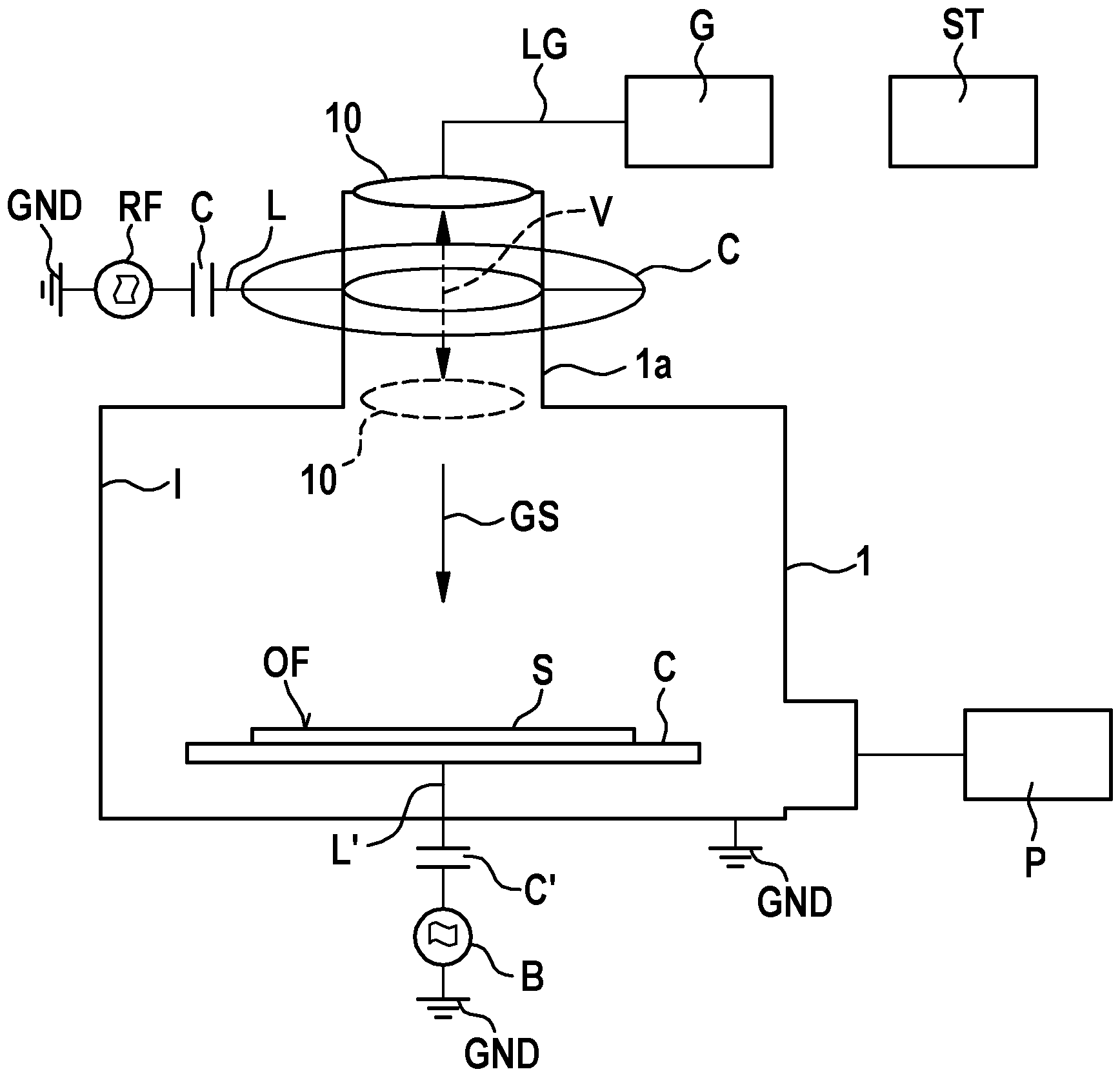
In
Angeschlossen an die Ätzkammer 1 ist eine Pumpeinrichtung P zum Erzeugen eines gewünschten Prozessdrucks und zum Abpumpen des Ätzgases, insbesondere wenn ein Wechsel des Ätzgases erforderlich ist. Der Chuck C ist mittels einer elektrischen Leitung L' über eine Kondesatoreinrichtung C' an eine Biaseinrichtung B angeschlossen, welche andererseits auf Massepotential GND liegt. Die Biaseinrichtung B dient zum Anlegen eines gewünschten elektrischen Potentials an den Chuck C, falls ein Sputterefekt erwünscht ist. Der Chuck ist vorzugsweise temperierbar, beispielsweise im Temperaturbereich zwischen -10 °C und 100 °C.Connected to the etching chamber 1 is a pumping device P for generating a desired process pressure and for pumping out the etching gas, in particular when a change of etching gas is required. The chuck C is connected by means of an electrical line L' via a capacitor device C' to a bias device B, which on the other hand is at ground potential GND. The bias device B is used to apply a desired electrical potential to the chuck C if a sputtering effect is desired. The chuck can preferably be tempered, for example in the temperature range between -10 °C and 100 °C.
Ebenfalls temperierbar ist eine Innenwand I der Ätzkammer 1, beispielsweise im selben Temperaturbereich zwischen -10 °C und 100 °C. Die Ätzkammer 1 weist im oberen Bereich einen verengten Bereich 1a auf, der von einer Plasmaerzeugungseinrichtung C umgeben ist welche eine kreisförmige Spuleneinrichtung umfasst, die über eine elektrische Leitung L und eine Kondensatoreinrichtung C und eine Radiofrequenzerzeugungseinrichtung RF angeschlossen ist, welche wiederum auf Massepotential GND liegt.An inner wall I of the etching chamber 1 can also be tempered, for example in the same temperature range between -10 °C and 100 °C. The etching chamber 1 has a narrowed
Bezugszeichen 10 bezeichnet einen Gasdüsen-Verteilungseinrichtung, welche am oberen Ende des verengten Bereichs 1a angeordnet ist und über die Ätzgas einleitbar ist, welches von einer Gasversorgungseinrichtung G über eine Leitungseinrichtung LG zugeführt wird. Die Leitungseinrichtung LG kann ebenfalls im Bereich zwischen -10 °C bis 100 °C temperierbar sein.
Die Gasversorgungseinrichtung G ist an mehrere (nicht dargestellte) Gasquellen angeschlossen, aus denen die jeweils benötigten Ätzgase entnommen werden können. Eine mit Bezugszeichen ST bezeichnete Steuereinrichtung sorgt für eine automatische Auswahl der benötigten Gasquelle, bzw. Ätzgasquellen und dient weiterhin einer Verstellbarkeit der Gasdüsen-Verteilungseinrichtung 10 in Abhängigkeit von einem gewählten Ätzmodus, welcher nachstehend näher beschrieben wird.The gas supply device G is connected to several gas sources (not shown) from which the required etching gases can be taken. A control device designated with the reference symbol ST ensures automatic selection of the required gas source or etching gas sources and also serves to adjust the gas
Die Gasdüsen-Verteilungseinrichtung 10 ist derart oberhalb des Chucks C angeordnet, dass ein Ätzgasstrom GS im Wesentlichen senkrecht auf die Oberfläche OF des zu ätzenden Substrats S gerichtet ist.The gas
Sie ist durch eine (nicht dargestellte) Aktuatoreinrichtung derart bezüglich der Oberfläche OF des zu ätzenden Substrats verfahrbar, dass sie in einem Plasmaätzmodus in einer derartigen ersten Entfernung von der Oberfläche OF angeordnet ist, dass der Ätzgasstrom GS durch den von der Plasmaerzeugungseinrichtung C umgebenen verengten Bereich 1a verläuft. Das hindurchtretende gewählte Ätzgas wird somit von der Plasmaerzeugungseinrichtung C aktiviert und gelangt dann zur Oberfläche OF des zu ätzenden Substrats S.It can be moved by an actuator device (not shown) in relation to the surface OF of the substrate to be etched in such a way that in a plasma etching mode it is arranged at a first distance from the surface OF such that the etching gas flow GS runs through the narrowed
In einem Nicht-Plasmaätzmodus hingegen wir die Gasdüsen-Verteilungseinrichtung 10 in Richtung der Oberfläche OF des Substrats hin durch den verengten Bereich 1a mit der umgebenen Plasmaerzeugungseinrichtung C verfahren, sodass sie sich in einer zweiten, geringeren Entfernung von der Oberfläche OF befindet, was für ein isotropes ätzen eine bessere Ätzbedingung bewirkt, da das Ätzvolumen verkleinert ist.In a non-plasma etching mode, however, the gas
Diese Verfahrbarkeit ist durch einen Doppelfall mit Bezugszeichen V schematisch angedeutet.This mobility is schematically indicated by a double case with reference symbol V.
Somit lassen sich durch entsprechende Programmierung der Steuereinrichtung ST alternierende plasmalose und plasmaunterstütze Ätzzyklen mit unterschiedlichen Ätzgasen einrichten.Thus, by appropriate programming of the ST control unit, alternating plasma-free and plasma-assisted etching cycles with different etching gases can be set up.
Für das plasmalose Ätzen können als Ätzgases beispielsweise XeF2 (Xenondifluorid) CIF (Chlorfluorid), CIF3 (Chlortrifluorid), CIF5 (Chlorpentafluorid), BF3 (Bromtrifluorid), BF5 (Brompentafluorid), IF5 (Jodpentafluorid), IF7 (Jodheptafluorid) als Ätzgas verwendet werden.For plasma-free etching, for example, XeF 2 (xenon difluoride), CIF (chlorine fluoride), CIF 3 (chlorine trifluoride), CIF 5 (chlorine pentafluoride), BF 3 (bromine trifluoride), BF 5 (bromine pentafluoride), IF 5 (iodine pentafluoride), IF 7 (iodine pentafluoride) can be used as etching gas.
Für eine plasmaunterstützes ätzen können beispielsweise F2 (Fluorgas), SF6 (Schwefelhexafluorid), CF4 (Kohlenstofftetrafluorid), CHF3 (Kohlenstoffwasserstofftrefluorid) CH2F3 (Kohlenstoffdiwasserstoffdifluorid), C2F6 (Dikohlenstoffhexafluorid), C3F8 (Trikohlenstoffoctafluorid) oder NF3 (Stickstofftrifluorid) usw. verwendet werden. Vorhergehende Ätzprozesse eignen sich insbesondere zum Opferschichtätzen.For plasma-assisted etching, for example, F 2 (fluorine gas), SF 6 (sulfur hexafluoride), CF 4 (carbon tetrafluoride), CHF 3 (hydrogen carbon tetrafluoride), CH 2 F 3 (carbon dihydrogen difluoride), C 2 F 6 (dicarbon hexafluoride), C 3 F 8 (tricarbon octafluoride) or NF 3 (nitrogen trifluoride) etc. can be used. Previous etching processes are particularly suitable for sacrificial layer etching.
Ein isotropes Öffnen von vergrabenen natürlichen SiO2 kann beispielsweise durch wasserfreies HF-Gas, Isopropanol etc. erreicht werden. Eine Polymerpassivierung ist beispielsweise mittels C4F8 (Tetrakohlenstoffoctafluorid) möglich.An isotropic opening of buried natural SiO 2 can be achieved, for example, by anhydrous HF gas, isopropanol, etc. Polymer passivation is possible, for example, using C 4 F 8 (tetracarbon octafluoride).
Als weitere Ätzgase sind Ar (Argon), N2 (Stickstoff), O2 (Sauerstoff), H2 (Wasserstoff), Cl2 (Chlorgas), Br2 (Bromgas), I2 (Jodgas), HCl (Chlorwasserstoffgas), HBr (Bromwasserstoffgas), HI (Jodwasserstoffgas) etc. vorstellbar.Other possible etching gases include Ar (argon), N 2 (nitrogen), O 2 (oxygen), H 2 (hydrogen), Cl 2 (chlorine gas), Br 2 (bromine gas), I 2 (iodine gas), HCl (hydrogen chloride gas), HBr (hydrogen bromide gas), HI (hydrogen iodide gas), etc.
Zweckmäßig ist es, dass alle Ätzvorgänge unter kontinuierlichem Fluss oder gepulstem Fluss möglich sind.It is practical that all etching processes can be carried out under continuous flow or pulsed flow.
Die Plasmaerzeugungseinrichtung C oberhalb des Substrats S weist typischerweise einen Abstand von 30 cm zur Oberfläche OF auf.The plasma generation device C above the substrate S is typically at a distance of 30 cm from the surface OF.
Weiterhin möglich ist ein in z-Höhenrichtung verfahrbarer Schutzring für den Rand des Substrats S (nicht dargestellt).It is also possible to have a protective ring for the edge of the substrate S that can be moved in the z-height direction (not shown).
Weiterhin möglich ist die Implementierung einer optischen Endpunkterkennung für sämtliche Ätzschritte.It is also possible to implement optical endpoint detection for all etching steps.
Gemäß der zweiten Ausführungsform sind im Unterschied zur oben beschriebenen ersten Ausführungsform eine erste Gasdüsen-Verteilungseinrichtung 10a und eine zweite Gasdüsen-Verteilungseinrichtung 10b vorgesehen.According to the second embodiment, in contrast to the first embodiment described above, a first gas
Die erste Gasdüsen-Verteilungseinrichtung 10a ist im Unterschied zur ersten Ausführungsform stationär oberhalb der Plasmaerzeugungseinrichtung C vorgesehen.In contrast to the first embodiment, the first gas
Die zweite Gasdüsen-Verteilungseinrichtung 10b ist in einer seitlichen Nische 1b der Ätzkammer 1 vorgesehen und weist eine Verfahrbarkeit V' entlang der mit dem Doppelpfeil gekennzeichneten Richtung also in der Zeichnung in horizontaler Richtung auf. Sie ist über eine Leitungseinrichtung LG' mit einer zweiten Gasversorgungseinrichtung G' verbunden.The second gas
Beim plasmaunterstützten Ätzen befindet sich die zweite Gasdüsen-Verteilungseinrichtung 10b in der Nische 1b und ist deaktiviert.During plasma-assisted etching, the second gas
Beim plasmaunterstützen Ätzen hingegen wird die erste Gasdüsen-Verteilungseinrichtung 10a deaktiviert und die zweite Gasdüsen-Verteilungseinrichtung 10b wird in waagrechter Richtung derart oberhalb der Oberfläche OF des Substrats verfahren, dass ein von ihr ausgehender Ätzgasstrom GS im Wesentlichen senkrecht auf die Oberfläche OF des zu ätzenden Substrats S gerichtet ist.In plasma-assisted etching, however, the first gas
Eine entsprechend modifizierte Steuereinrichtung ST' sorgt bei dieser zweiten Ausführungsform für die durch die Gasversorgungseinrichtungen G, G' bereitzustellenden Ätzgase und für die Verfahrbarkeit der zweiten Gasdüsen-Verteilungseinrichtung 10, sodass mit dieser Anordnung derselbe Effekt wie bei der oben beschriebenen ersten Ausführungsform erzielbar ist.In this second embodiment, a correspondingly modified control device ST' provides the etching gases to be provided by the gas supply devices G, G' and the mobility of the second gas
Bei der dritten Ausführungsform ist die Gasdüsen-Verteilungseinrichtung 10, welche oberhalb der Plasmaerzeugungseinrichtung angeordnet ist, ebenfalls stationär, jedoch lässt sich der Chuck C in Verfahrrichtung V'' derart verstellen, dass das Substrat S bei einem plasmalosen Ätzprozess näher an die Gasdüsen-Verteilungseinrichtung 10 bringbar ist. Somit ist auch bei dieser Ausführungsform derselbe Effekt wie bei der oben beschriebenen ersten und zweiten Ausführungsform erzielbar, nämlich eine Verringerung des Ätzvolumens beim plasmalosen Ätzen.In the third embodiment, the gas
Obwohl die vorliegende Erfindung anhand bevorzugter Ausführungsformen beschrieben wurde, ist sie nicht darauf beschränkt, sondern vielfältig modifizierbar.Although the present invention has been described using preferred embodiments, it is not limited thereto but can be modified in many ways.
Insbesondere ist es möglich, sowohl die Gasdüsen-Verteilungseinrichtung als auch den Chuck verstellbar zu gestalten, um beispielsweise das Ätzvolumen beim plasmalosen Ätzen noch weiter zu verringern.In particular, it is possible to make both the gas nozzle distribution device and the chuck adjustable in order to, for example, further reduce the etching volume during plasma-free etching.
Auch ist die Erfindung nicht auf die vorstehend genannten Ätzgase beschränkt, sondern prinzipiell für beliebige Ätzgase bzw. Passivierungsgase anwendbar.The invention is also not limited to the etching gases mentioned above, but is in principle applicable to any etching gases or passivation gases.
Des Weiteren ist es auch möglich, die Erfindung auf eine Ätzkammer anzuwenden, bei der eine Mehrzahl von Substraten gleichzeitig zu ätzen ist.Furthermore, it is also possible to apply the invention to an etching chamber in which a plurality of substrates are to be etched simultaneously.
Claims (14)
Priority Applications (4)
| Application Number | Priority Date | Filing Date | Title |
|---|---|---|---|
| DE102016200506.5A DE102016200506B4 (en) | 2016-01-17 | 2016-01-17 | Etching device and etching process |
| US15/402,648 US10020169B2 (en) | 2016-01-17 | 2017-01-10 | Etching device and etching method |
| TW106101386A TWI713077B (en) | 2016-01-17 | 2017-01-16 | Etching device and etching method |
| CN201710035322.3A CN107017148B (en) | 2016-01-17 | 2017-01-17 | Etching apparatus and etching method |
Applications Claiming Priority (1)
| Application Number | Priority Date | Filing Date | Title |
|---|---|---|---|
| DE102016200506.5A DE102016200506B4 (en) | 2016-01-17 | 2016-01-17 | Etching device and etching process |
Publications (2)
| Publication Number | Publication Date |
|---|---|
| DE102016200506A1 DE102016200506A1 (en) | 2017-07-20 |
| DE102016200506B4 true DE102016200506B4 (en) | 2024-05-02 |
Family
ID=59255982
Family Applications (1)
| Application Number | Title | Priority Date | Filing Date |
|---|---|---|---|
| DE102016200506.5A Active DE102016200506B4 (en) | 2016-01-17 | 2016-01-17 | Etching device and etching process |
Country Status (4)
| Country | Link |
|---|---|
| US (1) | US10020169B2 (en) |
| CN (1) | CN107017148B (en) |
| DE (1) | DE102016200506B4 (en) |
| TW (1) | TWI713077B (en) |
Families Citing this family (7)
| Publication number | Priority date | Publication date | Assignee | Title |
|---|---|---|---|---|
| DE102016200506B4 (en) * | 2016-01-17 | 2024-05-02 | Robert Bosch Gmbh | Etching device and etching process |
| CN107919277A (en) * | 2016-10-08 | 2018-04-17 | 北京北方华创微电子装备有限公司 | Method and manufacturing process for removing silicon dioxide on wafer |
| CN107845574B (en) * | 2017-10-31 | 2018-11-23 | 长鑫存储技术有限公司 | The method of etching removal oxide on semiconductor |
| JP7072440B2 (en) * | 2018-05-16 | 2022-05-20 | 東京エレクトロン株式会社 | Etching method for silicon-containing film, computer storage medium, and etching device for silicon-containing film |
| JP7174180B2 (en) * | 2018-05-16 | 2022-11-17 | 東京エレクトロン株式会社 | Silicon-containing film etching method, computer storage medium, and silicon-containing film etching apparatus |
| CN112117176B (en) * | 2019-06-20 | 2023-03-07 | 中微半导体设备(上海)股份有限公司 | Plasma processing apparatus and plasma processing system |
| CN118204316A (en) * | 2024-04-18 | 2024-06-18 | 中南大学 | Aluminum surface paint removal device, removal method and application |
Citations (6)
| Publication number | Priority date | Publication date | Assignee | Title |
|---|---|---|---|---|
| DE19840437A1 (en) | 1997-12-05 | 1999-06-17 | Samsung Electronics Co Ltd | Etching process for polysilicon and etching device |
| US6221784B1 (en) | 1999-11-29 | 2001-04-24 | Applied Materials Inc. | Method and apparatus for sequentially etching a wafer using anisotropic and isotropic etching |
| WO2002095800A2 (en) | 2001-05-22 | 2002-11-28 | Reflectivity, Inc. | A method for making a micromechanical device by removing a sacrificial layer with multiple sequential etchants |
| US20020195423A1 (en) | 1999-10-26 | 2002-12-26 | Reflectivity, Inc. | Method for vapor phase etching of silicon |
| DE69934986T2 (en) | 1998-07-23 | 2007-11-08 | Surface Technoloy Systems Plc | PROCESS FOR ANISOTROPIC CORES |
| US20130210241A1 (en) | 2012-02-14 | 2013-08-15 | Novellus Systems Inc. | Precursors for Plasma Activated Conformal Film Deposition |
Family Cites Families (21)
| Publication number | Priority date | Publication date | Assignee | Title |
|---|---|---|---|---|
| DE10209763A1 (en) * | 2002-03-05 | 2003-10-02 | Bosch Gmbh Robert | Device and method for anisotropic plasma etching of a substrate, in particular a silicon body |
| US7358192B2 (en) * | 2004-04-08 | 2008-04-15 | Applied Materials, Inc. | Method and apparatus for in-situ film stack processing |
| US20060162661A1 (en) * | 2005-01-22 | 2006-07-27 | Applied Materials, Inc. | Mixing energized and non-energized gases for silicon nitride deposition |
| US7608549B2 (en) * | 2005-03-15 | 2009-10-27 | Asm America, Inc. | Method of forming non-conformal layers |
| US8039052B2 (en) * | 2007-09-06 | 2011-10-18 | Intermolecular, Inc. | Multi-region processing system and heads |
| US8726838B2 (en) * | 2010-03-31 | 2014-05-20 | Intermolecular, Inc. | Combinatorial plasma enhanced deposition and etch techniques |
| JP5075793B2 (en) * | 2008-11-06 | 2012-11-21 | 東京エレクトロン株式会社 | Movable gas introduction structure and substrate processing apparatus |
| JP5643528B2 (en) * | 2009-03-30 | 2014-12-17 | 東京エレクトロン株式会社 | Substrate processing equipment |
| US8592328B2 (en) * | 2012-01-20 | 2013-11-26 | Novellus Systems, Inc. | Method for depositing a chlorine-free conformal sin film |
| KR101984524B1 (en) * | 2012-07-06 | 2019-05-31 | 주성엔지니어링(주) | Apparatus of processing substrate |
| US20140110764A1 (en) * | 2012-10-19 | 2014-04-24 | Intermolecular Inc. | Method to control amorphous oxide layer formation at interfaces of thin film stacks for memory and logic components |
| US8822313B2 (en) * | 2012-12-20 | 2014-09-02 | Intermolecular, Inc. | Surface treatment methods and systems for substrate processing |
| US9790090B2 (en) * | 2013-02-13 | 2017-10-17 | Lawrence Livermore National Security, Llc | Laser-induced gas plasma machining |
| US20140262028A1 (en) * | 2013-03-13 | 2014-09-18 | Intermolecular, Inc. | Non-Contact Wet-Process Cell Confining Liquid to a Region of a Solid Surface by Differential Pressure |
| US8945414B1 (en) * | 2013-11-13 | 2015-02-03 | Intermolecular, Inc. | Oxide removal by remote plasma treatment with fluorine and oxygen radicals |
| US9101038B2 (en) * | 2013-12-20 | 2015-08-04 | Lam Research Corporation | Electrostatic chuck including declamping electrode and method of declamping |
| JP6410622B2 (en) * | 2014-03-11 | 2018-10-24 | 東京エレクトロン株式会社 | Plasma processing apparatus and film forming method |
| US20170301958A1 (en) * | 2014-10-03 | 2017-10-19 | Su Xiang Deng | Plasma deposition to fabricate lithium batteries |
| US10566187B2 (en) * | 2015-03-20 | 2020-02-18 | Lam Research Corporation | Ultrathin atomic layer deposition film accuracy thickness control |
| DE102016200506B4 (en) * | 2016-01-17 | 2024-05-02 | Robert Bosch Gmbh | Etching device and etching process |
| US10651080B2 (en) * | 2016-04-26 | 2020-05-12 | Lam Research Corporation | Oxidizing treatment of aluminum nitride films in semiconductor device manufacturing |
-
2016
- 2016-01-17 DE DE102016200506.5A patent/DE102016200506B4/en active Active
-
2017
- 2017-01-10 US US15/402,648 patent/US10020169B2/en active Active
- 2017-01-16 TW TW106101386A patent/TWI713077B/en active
- 2017-01-17 CN CN201710035322.3A patent/CN107017148B/en active Active
Patent Citations (6)
| Publication number | Priority date | Publication date | Assignee | Title |
|---|---|---|---|---|
| DE19840437A1 (en) | 1997-12-05 | 1999-06-17 | Samsung Electronics Co Ltd | Etching process for polysilicon and etching device |
| DE69934986T2 (en) | 1998-07-23 | 2007-11-08 | Surface Technoloy Systems Plc | PROCESS FOR ANISOTROPIC CORES |
| US20020195423A1 (en) | 1999-10-26 | 2002-12-26 | Reflectivity, Inc. | Method for vapor phase etching of silicon |
| US6221784B1 (en) | 1999-11-29 | 2001-04-24 | Applied Materials Inc. | Method and apparatus for sequentially etching a wafer using anisotropic and isotropic etching |
| WO2002095800A2 (en) | 2001-05-22 | 2002-11-28 | Reflectivity, Inc. | A method for making a micromechanical device by removing a sacrificial layer with multiple sequential etchants |
| US20130210241A1 (en) | 2012-02-14 | 2013-08-15 | Novellus Systems Inc. | Precursors for Plasma Activated Conformal Film Deposition |
Also Published As
| Publication number | Publication date |
|---|---|
| US20170207067A1 (en) | 2017-07-20 |
| DE102016200506A1 (en) | 2017-07-20 |
| US10020169B2 (en) | 2018-07-10 |
| CN107017148A (en) | 2017-08-04 |
| TW201735094A (en) | 2017-10-01 |
| TWI713077B (en) | 2020-12-11 |
| CN107017148B (en) | 2020-12-25 |
Similar Documents
| Publication | Publication Date | Title |
|---|---|---|
| DE102016200506B4 (en) | Etching device and etching process | |
| DE69736969T2 (en) | Method of treating the surface of semiconductive substrates | |
| DE102005047081B4 (en) | Process for the plasma-free etching of silicon with the etching gas ClF3 or XeF2 | |
| DE112015001462B4 (en) | A method of operating an etch process device for a silicon etch process | |
| DE69725245T2 (en) | Process for etching substrates | |
| EP1062180A1 (en) | Method for processing silicon using etching processes | |
| EP2313913B1 (en) | Method for electron beam induced etching of layers implanted with gallium | |
| EP0625285A1 (en) | Method for anisotropically etching silicon | |
| DE4133332A1 (en) | METHOD FOR ETCHING SEMICONDUCTOR COMPONENTS | |
| DE102009028256B4 (en) | A method of etching silicon carbide using a plasma etching method and silicon carbide substrate | |
| US11024515B2 (en) | Systems and methods for in SITU maintenance of a thin hardmask during an etch process | |
| DE4202447A1 (en) | Trench profile with vertical walls - formed by dry etching using ambient contg. ammonia to produce passivation layer on trench walls | |
| DE112018003719B4 (en) | CUTTING PROCESS | |
| DE102012200236B3 (en) | Method for structuring silicon carbide for e.g. silicon carbide-trench-MOSFET, involves reperforming anisotropic plasma etching step such that passivation layer is removed from trench bottom, and forming enlarged trench region in substrate | |
| DE102013223490A1 (en) | Process for producing a structured surface | |
| WO2004093162A2 (en) | Silicon substrate comprising positive etching profiles with a defined slope angle, and production method | |
| EP1527011B1 (en) | Layer system with a silicon layer and a passivation layer, method for production of a passivation layer on a silicon layer and use thereof | |
| DE102016220248A1 (en) | APPARATUS AND METHOD FOR ANISOTROPIC DRY EQUIPMENT FLUORESCENT MIXING | |
| EP1522094A1 (en) | Method for structuring metal by means of a carbon mask | |
| DE19841964B4 (en) | Process for adjusting the etching speed in anisotropic plasma etching of lateral structures | |
| EP2084734A1 (en) | Plasma etching method for producing positive etching profiles in silicon substrates | |
| DE102016200504B4 (en) | sacrificial layer etching process | |
| DE102024205736A1 (en) | Micromechanical device and method for manufacturing a micromechanical device with at least one MEMS component, a MEMS substrate, a MEMS layer structure having functional structures, a cap part and a pressure access structure | |
| DE102011012087B3 (en) | Semiconductor structure e.g. PNP-semiconductor structure, manufacturing method, involves accelerating ions by acceleration voltage, where ions acceleration and plasma generation are independently controlled from each other | |
| DE19945140A1 (en) | Process for producing a mask layer with openings of reduced width |
Legal Events
| Date | Code | Title | Description |
|---|---|---|---|
| R012 | Request for examination validly filed | ||
| R016 | Response to examination communication | ||
| R018 | Grant decision by examination section/examining division | ||
| R020 | Patent grant now final | ||
| R079 | Amendment of ipc main class |
Free format text: PREVIOUS MAIN CLASS: H01L0021306000 Ipc: H10P0050000000 |