DE102016103324A1 - Video wall module and method of making a video wall module - Google Patents
Video wall module and method of making a video wall module Download PDFInfo
- Publication number
- DE102016103324A1 DE102016103324A1 DE102016103324.3A DE102016103324A DE102016103324A1 DE 102016103324 A1 DE102016103324 A1 DE 102016103324A1 DE 102016103324 A DE102016103324 A DE 102016103324A DE 102016103324 A1 DE102016103324 A1 DE 102016103324A1
- Authority
- DE
- Germany
- Prior art keywords
- circuit board
- video wall
- wall module
- metallization layer
- printed circuit
- Prior art date
- Legal status (The legal status is an assumption and is not a legal conclusion. Google has not performed a legal analysis and makes no representation as to the accuracy of the status listed.)
- Withdrawn
Links
Images


Classifications
-
- G—PHYSICS
- G09—EDUCATION; CRYPTOGRAPHY; DISPLAY; ADVERTISING; SEALS
- G09F—DISPLAYING; ADVERTISING; SIGNS; LABELS OR NAME-PLATES; SEALS
- G09F9/00—Indicating arrangements for variable information in which the information is built-up on a support by selection or combination of individual elements
- G09F9/30—Indicating arrangements for variable information in which the information is built-up on a support by selection or combination of individual elements in which the desired character or characters are formed by combining individual elements
- G09F9/302—Indicating arrangements for variable information in which the information is built-up on a support by selection or combination of individual elements in which the desired character or characters are formed by combining individual elements characterised by the form or geometrical disposition of the individual elements
- G09F9/3026—Video wall, i.e. stackable semiconductor matrix display modules
-
- G—PHYSICS
- G09—EDUCATION; CRYPTOGRAPHY; DISPLAY; ADVERTISING; SEALS
- G09G—ARRANGEMENTS OR CIRCUITS FOR CONTROL OF INDICATING DEVICES USING STATIC MEANS TO PRESENT VARIABLE INFORMATION
- G09G3/00—Control arrangements or circuits, of interest only in connection with visual indicators other than cathode-ray tubes
- G09G3/20—Control arrangements or circuits, of interest only in connection with visual indicators other than cathode-ray tubes for presentation of an assembly of a number of characters, e.g. a page, by composing the assembly by combination of individual elements arranged in a matrix no fixed position being assigned to or needed to be assigned to the individual characters or partial characters
- G09G3/22—Control arrangements or circuits, of interest only in connection with visual indicators other than cathode-ray tubes for presentation of an assembly of a number of characters, e.g. a page, by composing the assembly by combination of individual elements arranged in a matrix no fixed position being assigned to or needed to be assigned to the individual characters or partial characters using controlled light sources
- G09G3/30—Control arrangements or circuits, of interest only in connection with visual indicators other than cathode-ray tubes for presentation of an assembly of a number of characters, e.g. a page, by composing the assembly by combination of individual elements arranged in a matrix no fixed position being assigned to or needed to be assigned to the individual characters or partial characters using controlled light sources using electroluminescent panels
- G09G3/32—Control arrangements or circuits, of interest only in connection with visual indicators other than cathode-ray tubes for presentation of an assembly of a number of characters, e.g. a page, by composing the assembly by combination of individual elements arranged in a matrix no fixed position being assigned to or needed to be assigned to the individual characters or partial characters using controlled light sources using electroluminescent panels semiconductive, e.g. using light-emitting diodes [LED]
-
- H—ELECTRICITY
- H05—ELECTRIC TECHNIQUES NOT OTHERWISE PROVIDED FOR
- H05K—PRINTED CIRCUITS; CASINGS OR CONSTRUCTIONAL DETAILS OF ELECTRIC APPARATUS; MANUFACTURE OF ASSEMBLAGES OF ELECTRICAL COMPONENTS
- H05K3/00—Apparatus or processes for manufacturing printed circuits
- H05K3/30—Assembling printed circuits with electric components, e.g. with resistor
- H05K3/32—Assembling printed circuits with electric components, e.g. with resistor electrically connecting electric components or wires to printed circuits
- H05K3/321—Assembling printed circuits with electric components, e.g. with resistor electrically connecting electric components or wires to printed circuits by conductive adhesives
- H05K3/323—Assembling printed circuits with electric components, e.g. with resistor electrically connecting electric components or wires to printed circuits by conductive adhesives by applying an anisotropic conductive adhesive layer over an array of pads
-
- H—ELECTRICITY
- H10—SEMICONDUCTOR DEVICES; ELECTRIC SOLID-STATE DEVICES NOT OTHERWISE PROVIDED FOR
- H10H—INORGANIC LIGHT-EMITTING SEMICONDUCTOR DEVICES HAVING POTENTIAL BARRIERS
- H10H20/00—Individual inorganic light-emitting semiconductor devices having potential barriers, e.g. light-emitting diodes [LED]
- H10H20/80—Constructional details
- H10H20/83—Electrodes
-
- H—ELECTRICITY
- H10—SEMICONDUCTOR DEVICES; ELECTRIC SOLID-STATE DEVICES NOT OTHERWISE PROVIDED FOR
- H10H—INORGANIC LIGHT-EMITTING SEMICONDUCTOR DEVICES HAVING POTENTIAL BARRIERS
- H10H20/00—Individual inorganic light-emitting semiconductor devices having potential barriers, e.g. light-emitting diodes [LED]
- H10H20/80—Constructional details
- H10H20/85—Packages
- H10H20/852—Encapsulations
- H10H20/853—Encapsulations characterised by their shape
-
- H—ELECTRICITY
- H10—SEMICONDUCTOR DEVICES; ELECTRIC SOLID-STATE DEVICES NOT OTHERWISE PROVIDED FOR
- H10H—INORGANIC LIGHT-EMITTING SEMICONDUCTOR DEVICES HAVING POTENTIAL BARRIERS
- H10H20/00—Individual inorganic light-emitting semiconductor devices having potential barriers, e.g. light-emitting diodes [LED]
- H10H20/80—Constructional details
- H10H20/85—Packages
- H10H20/857—Interconnections, e.g. lead-frames, bond wires or solder balls
-
- H10W70/611—
-
- H10W70/65—
-
- H10W70/685—
-
- H10W90/00—
-
- G—PHYSICS
- G09—EDUCATION; CRYPTOGRAPHY; DISPLAY; ADVERTISING; SEALS
- G09G—ARRANGEMENTS OR CIRCUITS FOR CONTROL OF INDICATING DEVICES USING STATIC MEANS TO PRESENT VARIABLE INFORMATION
- G09G2300/00—Aspects of the constitution of display devices
- G09G2300/02—Composition of display devices
- G09G2300/026—Video wall, i.e. juxtaposition of a plurality of screens to create a display screen of bigger dimensions
-
- G—PHYSICS
- G09—EDUCATION; CRYPTOGRAPHY; DISPLAY; ADVERTISING; SEALS
- G09G—ARRANGEMENTS OR CIRCUITS FOR CONTROL OF INDICATING DEVICES USING STATIC MEANS TO PRESENT VARIABLE INFORMATION
- G09G2300/00—Aspects of the constitution of display devices
- G09G2300/04—Structural and physical details of display devices
- G09G2300/0421—Structural details of the set of electrodes
- G09G2300/0426—Layout of electrodes and connections
-
- G—PHYSICS
- G09—EDUCATION; CRYPTOGRAPHY; DISPLAY; ADVERTISING; SEALS
- G09G—ARRANGEMENTS OR CIRCUITS FOR CONTROL OF INDICATING DEVICES USING STATIC MEANS TO PRESENT VARIABLE INFORMATION
- G09G2300/00—Aspects of the constitution of display devices
- G09G2300/04—Structural and physical details of display devices
- G09G2300/0439—Pixel structures
- G09G2300/0452—Details of colour pixel setup, e.g. pixel composed of a red, a blue and two green components
-
- G—PHYSICS
- G09—EDUCATION; CRYPTOGRAPHY; DISPLAY; ADVERTISING; SEALS
- G09G—ARRANGEMENTS OR CIRCUITS FOR CONTROL OF INDICATING DEVICES USING STATIC MEANS TO PRESENT VARIABLE INFORMATION
- G09G2300/00—Aspects of the constitution of display devices
- G09G2300/06—Passive matrix structure, i.e. with direct application of both column and row voltages to the light emitting or modulating elements, other than LCD or OLED
-
- H—ELECTRICITY
- H05—ELECTRIC TECHNIQUES NOT OTHERWISE PROVIDED FOR
- H05K—PRINTED CIRCUITS; CASINGS OR CONSTRUCTIONAL DETAILS OF ELECTRIC APPARATUS; MANUFACTURE OF ASSEMBLAGES OF ELECTRICAL COMPONENTS
- H05K1/00—Printed circuits
- H05K1/02—Details
- H05K1/0296—Conductive pattern lay-out details not covered by sub groups H05K1/02 - H05K1/0295
- H05K1/0298—Multilayer circuits
-
- H—ELECTRICITY
- H05—ELECTRIC TECHNIQUES NOT OTHERWISE PROVIDED FOR
- H05K—PRINTED CIRCUITS; CASINGS OR CONSTRUCTIONAL DETAILS OF ELECTRIC APPARATUS; MANUFACTURE OF ASSEMBLAGES OF ELECTRICAL COMPONENTS
- H05K1/00—Printed circuits
- H05K1/18—Printed circuits structurally associated with non-printed electric components
- H05K1/181—Printed circuits structurally associated with non-printed electric components associated with surface mounted components
-
- H—ELECTRICITY
- H05—ELECTRIC TECHNIQUES NOT OTHERWISE PROVIDED FOR
- H05K—PRINTED CIRCUITS; CASINGS OR CONSTRUCTIONAL DETAILS OF ELECTRIC APPARATUS; MANUFACTURE OF ASSEMBLAGES OF ELECTRICAL COMPONENTS
- H05K2201/00—Indexing scheme relating to printed circuits covered by H05K1/00
- H05K2201/10—Details of components or other objects attached to or integrated in a printed circuit board
- H05K2201/10007—Types of components
- H05K2201/10106—Light emitting diode [LED]
-
- H—ELECTRICITY
- H05—ELECTRIC TECHNIQUES NOT OTHERWISE PROVIDED FOR
- H05K—PRINTED CIRCUITS; CASINGS OR CONSTRUCTIONAL DETAILS OF ELECTRIC APPARATUS; MANUFACTURE OF ASSEMBLAGES OF ELECTRICAL COMPONENTS
- H05K3/00—Apparatus or processes for manufacturing printed circuits
- H05K3/22—Secondary treatment of printed circuits
- H05K3/28—Applying non-metallic protective coatings
- H05K3/284—Applying non-metallic protective coatings for encapsulating mounted components
-
- H—ELECTRICITY
- H10—SEMICONDUCTOR DEVICES; ELECTRIC SOLID-STATE DEVICES NOT OTHERWISE PROVIDED FOR
- H10H—INORGANIC LIGHT-EMITTING SEMICONDUCTOR DEVICES HAVING POTENTIAL BARRIERS
- H10H20/00—Individual inorganic light-emitting semiconductor devices having potential barriers, e.g. light-emitting diodes [LED]
- H10H20/01—Manufacture or treatment
- H10H20/036—Manufacture or treatment of packages
- H10H20/0362—Manufacture or treatment of packages of encapsulations
-
- H—ELECTRICITY
- H10—SEMICONDUCTOR DEVICES; ELECTRIC SOLID-STATE DEVICES NOT OTHERWISE PROVIDED FOR
- H10H—INORGANIC LIGHT-EMITTING SEMICONDUCTOR DEVICES HAVING POTENTIAL BARRIERS
- H10H20/00—Individual inorganic light-emitting semiconductor devices having potential barriers, e.g. light-emitting diodes [LED]
- H10H20/01—Manufacture or treatment
- H10H20/036—Manufacture or treatment of packages
- H10H20/0364—Manufacture or treatment of packages of interconnections
-
- H10W72/01357—
-
- H10W72/07311—
-
- H10W72/07331—
-
- H10W90/734—
Landscapes
- Engineering & Computer Science (AREA)
- Physics & Mathematics (AREA)
- General Physics & Mathematics (AREA)
- Theoretical Computer Science (AREA)
- Computer Hardware Design (AREA)
- Microelectronics & Electronic Packaging (AREA)
- Manufacturing & Machinery (AREA)
- Multimedia (AREA)
- Power Engineering (AREA)
- Led Device Packages (AREA)
- Condensed Matter Physics & Semiconductors (AREA)
- Devices For Indicating Variable Information By Combining Individual Elements (AREA)
- Geometry (AREA)
- Planar Illumination Modules (AREA)
Abstract
Ein Videowand-Modul umfasst eine Mehrzahl von Leuchtdiodenchips, die jeweils an einer Kontaktseite angeordnete erste Kontaktelektroden und zweite Kontaktelektroden aufweisen. Die Leuchtdiodenchips sind an einer Oberseite einer mehrlagigen Leiterplatte angeordnet. Die Kontaktelektroden sind elektrisch leitend mit einer an der Oberseite der Leiterplatte angeordneten ersten Metallisierungslage verbunden.A video wall module comprises a plurality of light-emitting diode chips, which each have first contact electrodes arranged on a contact side and second contact electrodes. The light-emitting diode chips are arranged on an upper side of a multilayer printed circuit board. The contact electrodes are electrically conductively connected to a arranged on the upper side of the circuit board first metallization.
Description
Die vorliegende Erfindung betrifft ein Videowand-Modul sowie ein Verfahren zum Herstellen eines Videowand-Moduls.The present invention relates to a video wall module and to a method for producing a video wall module.
Videowand-Module zum Aufbau von Videowänden sind aus dem Stand der Technik bekannt. Videowände sind Anzeigetafeln für statische oder bewegte Bilder, bei denen jeder Bildpunkt (Pixel) durch einen oder mehrere Leuchtdiodenchips (LED-Chips) gebildet wird. Zum Erreichen einer hohen Anzeigequalität sind kleine Abstände der Bildpunkte voneinander, ein hoher Kontrast und eine gleichmäßige Lichtabstrahlung in unterschiedliche Raumrichtungen wünschenswert.Video wall modules for building video walls are known from the prior art. Video walls are display panels for static or moving images in which each pixel is formed by one or more light emitting diode (LED) chips. To achieve a high display quality, small distances of the pixels from each other, a high contrast and a uniform light emission in different spatial directions are desirable.
Eine Aufgabe der vorliegenden Erfindung besteht darin, ein Videowand-Modul bereitzustellen. Eine weitere Aufgabe der vorliegenden Erfindung besteht darin, ein Verfahren zum Herstellen eines Videowand-Moduls anzugeben. Diese Aufgaben werden durch ein Videowand-Modul und ein Verfahren zum Herstellen eines Videowand-Moduls gemäß den unabhängigen Ansprüchen gelöst. In den abhängigen Ansprüchen sind verschiedene Weiterbildungen angegeben.An object of the present invention is to provide a video wall module. Another object of the present invention is to provide a method of making a video wall module. These objects are achieved by a video wall module and a method for producing a video wall module according to the independent claims. In the dependent claims various developments are given.
Ein Videowand-Modul umfasst eine Mehrzahl von Leuchtdiodenchips, die jeweils an einer Kontaktseite angeordnete erste Kontaktelektroden und zweite Kontaktelektroden aufweisen. Die Leuchtdiodenchips sind an einer Oberseite einer mehrlagigen Leiterplatte angeordnet. Die Kontaktelektroden sind elektrisch leitend mit einer an der Oberseite der Leiterplatte angeordneten ersten Metallisierungslage verbunden.A video wall module comprises a plurality of light-emitting diode chips, which each have first contact electrodes arranged on a contact side and second contact electrodes. The light-emitting diode chips are arranged on an upper side of a multilayer printed circuit board. The contact electrodes are electrically conductively connected to a arranged on the upper side of the circuit board first metallization.
Vorteilhafterweise sind bei den Leuchtdiodenchips dieses Videowand-Moduls die ersten Kontaktelektroden und die zweiten Kontaktelektroden an denselben Seiten der Leuchtdiodenchips angeordnet. Hierdurch können die Leuchtdiodenchips bei diesem Videowand-Modul auf einfache Weise elektrisch kontaktiert werden. Insbesondere sind bei diesem Videowand-Modul keine oberhalb der Leuchtdiodenchips angeordneten Kontaktierungsstrukturen erforderlich. Hierdurch kann das Videowand-Modul kostengünstig hergestellt werden und ist robust und unempfindlich gegenüber Beschädigungen ausgebildet.Advantageously, in the light-emitting diode chips of this video wall module, the first contact electrodes and the second contact electrodes are arranged on the same sides of the light-emitting diode chips. As a result, the light-emitting diode chips in this video wall module can be contacted electrically in a simple manner. In particular, in this video wall module, no contacting structures arranged above the light-emitting diode chips are required. As a result, the video wall module can be produced inexpensively and is robust and insensitive to damage.
In einer Ausführungsform des Videowand-Moduls ist an der Kontaktseite jedes Leuchtdiodenchips jeweils ein strukturierter Abschnitt eines Conductive-Die-Attach-Films angeordnet, der die Kontaktelektroden des Leuchtdiodenchips elektrisch leitend mit der ersten Metallisierungslage verbindet. Vorteilhafterweise ermöglicht dies eine einfache und zuverlässige elektrische Kontaktierung der Leuchtdiodenchips auch in dem Fall, dass die Leuchtdiodenchips sehr kleine Kantenlängen aufweisen und die Kontaktelektroden der Leuchtdiodenchips sehr nah beieinander angeordnet sind. Insbesondere können durch das Vorsehen der Abschnitte des Conductive-Die-Attach-Films zur Herstellung der elektrisch leitenden Verbindungen zwischen den Kontaktelektroden der Leuchtdiodenchips und der ersten Metallisierungslage elektrische Kurzschlüsse zwischen den Kontaktelektroden der Leuchtdiodenchips vermieden werden.In one embodiment of the video wall module, a structured section of a conductive die-attach film, which connects the contact electrodes of the light-emitting diode chip in an electrically conductive manner to the first metallization layer, is arranged on the contact side of each light-emitting diode chip. Advantageously, this allows a simple and reliable electrical contacting of the LED chips also in the case that the LED chips have very small edge lengths and the contact electrodes of the LED chips are arranged very close to each other. In particular, by providing the portions of the conductive die-attach film for making the electrically conductive connections between the contact electrodes of the LED chips and the first metallization layer, electrical short circuits between the contact electrodes of the LED chips can be avoided.
In einer Ausführungsform des Videowand-Moduls ist an der Oberseite der Leiterplatte eine anisotrop leitende Folie angeordnet, die die Kontaktelektroden der Leuchtdiodenchips elektrisch leitend mit der ersten Metallisierungslage verbindet. Vorteilhafterweise ermöglicht das Vorsehen der anisotrop leitenden Folie eine einfache und zuverlässig elektrische Kontaktierung der Leuchtdiodenchips auch in dem Fall, dass die Leuchtdiodenchips kleine Kantenlängen aufweisen. Insbesondere kann durch das Vorsehen der anisotrop leitenden Folie ein Auftreten von Kurzschlüssen zwischen den Kontaktelektroden der Leuchtdiodenchips verhindert werden.In one embodiment of the video wall module, an anisotropically conductive film is arranged on the upper side of the printed circuit board and connects the contact electrodes of the light-emitting diode chips to the first metallization layer in an electrically conductive manner. Advantageously, the provision of the anisotropically conductive foil allows a simple and reliable electrical contacting of the light-emitting diode chips even in the case that the light-emitting diode chips have small edge lengths. In particular, by providing the anisotropically conductive film, an occurrence of short circuits between the contact electrodes of the LED chips can be prevented.
In einer Ausführungsform des Videowand-Moduls sind die Leuchtdiodenchips zumindest teilweise in ein an der Oberseite der Leiterplatte angeordnetes Vergussmaterial eingebettet. In one embodiment of the video wall module, the light-emitting diode chips are at least partially embedded in a potting material arranged on the upper side of the printed circuit board.
Vorteilhafterweise sind die Leuchtdiodenchips dadurch vor einer Beschädigung durch äußere Einwirkungen geschützt. Das Vergussmaterial bildet außerdem eine vorteilhafte, glatte und einheitliche Oberfläche an der Oberseite des Videowand-Moduls, die, je nach Anwendungsfall, eine gewünschte hohe oder niedrige optische Reflektivität aufweisen kann. Hierzu kann das Vergussmaterial mit geeigneten optischen Reflexionseigenschaften gewählt werden.Advantageously, the light-emitting diode chips are thereby protected against damage due to external influences. The potting material also provides an advantageous, smooth and uniform surface at the top of the video wall module, which, depending on the application, may have a desired high or low optical reflectivity. For this purpose, the potting material can be selected with suitable optical reflection properties.
In einer Ausführungsform des Videowand-Moduls weist die Leiterplatte eine zweite Metallisierungslage auf. Dabei sind Abschnitte der ersten Metallisierungslage und Abschnitte der zweiten Metallisierungslage durch in der Leiterplatte angeordnete Durchkontakte elektrisch leitend miteinander verbunden. Vorteilhafterweise ermöglichen die Metallisierungslagen der Leiterplatte des Videowand-Moduls eine komplexe elektrische Verschaltung der Leuchtdiodenchips des Videowand-Moduls. Insbesondere werden durch das Vorhandensein einer ersten Metallisierungslage und einer zweiten Metallisierungslage auch Leitungskreuzungen ermöglicht.In one embodiment of the video wall module, the circuit board has a second metallization layer. In this case, sections of the first metallization layer and sections of the second metallization layer are electrically conductively connected to one another by through contacts arranged in the printed circuit board. Advantageously, the metallization layers of the printed circuit board of the video wall module enable a complex electrical connection of the light-emitting diode chips of the video wall module. In particular, line crossings are made possible by the presence of a first metallization layer and a second metallization layer.
In einer Ausführungsform des Videowand-Moduls sind die Leuchtdiodenchips logisch auf Zeilen und Spalten einer Matrix verteilt. Dabei sind die ersten Kontaktelektroden der Leuchtdiodenchips durch die erste Metallisierungslage spaltenweise elektrisch leitend miteinander verbunden. Die zweiten Kontaktelektroden der Leuchtdiodenchips sind durch die zweite Metallisierungslage zeilenweise elektrisch leitend miteinander verbunden. Die Leuchtdiodenchips des Videowand-Moduls sind damit in einer Kreuzmatrix-Verschaltung angeordnet. Diese ermöglicht es vorteilhafterweise, alle Leuchtdiodenchips einer logischen Zeile der Matrix gleichzeitig unabhängig voneinander anzusteuern, während die Leuchtdiodenchips der übrigen Zeilen der Matrix nicht angesteuert werden. Die einzelnen Zeilen der Matrix können zeitlich nacheinander im Multiplex-Betrieb angesteuert werden. Hierzu wird es ermöglicht, jeden der Leuchtdiodenchips des Videowand-Moduls unabhängig von den übrigen Leuchtdiodenchips des Videowand-Moduls zu betreiben, ohne dass für jeden Leuchtdiodenchip des Videowand-Moduls eigene, unabhängige Steuerleitungen vorgesehen werden müssen.In one embodiment of the video wall module, the LED chips are logically distributed on rows and columns of a matrix. In this case, the first contact electrodes of the light-emitting diode chips are electrically conductive in columns by the first metallization layer conductively connected. The second contact electrodes of the LED chips are connected by the second metallization layer line by line electrically conductive. The LED chips of the video wall module are thus arranged in a cross-matrix interconnection. This advantageously makes it possible to control all light-emitting diode chips of one logical row of the matrix simultaneously independently of one another, while the light-emitting diode chips of the remaining rows of the matrix are not driven. The individual lines of the matrix can be controlled one after the other in multiplex mode. For this purpose, it is possible to operate each of the light-emitting diode chips of the video wall module independently of the remaining light-emitting diode chips of the video wall module without having to provide separate, independent control lines for each light-emitting diode chip of the video wall module.
In einer Ausführungsform des Videowand-Moduls weist die Leiterplatte eine dritte Metallisierungslage auf. Dabei sind Abschnitte der zweiten Metallisierungslage und Abschnitte der dritten Metallisierungslage durch in der Leiterplatte angeordnete Durchkontakte elektrisch leitend miteinander verbunden. Vorteilhafterweise bietet das Vorsehen der dritten Metallisierungslage zusätzliche Freiheitsgrade bei der Gestaltung der elektrischen Schnittstelle des Videowand-Moduls.In one embodiment of the video wall module, the circuit board has a third metallization layer. In this case, sections of the second metallization layer and sections of the third metallization layer are electrically conductively connected to one another by through contacts arranged in the printed circuit board. Advantageously, the provision of the third metallization layer provides additional degrees of freedom in designing the electrical interface of the video wall module.
In einer Ausführungsform des Videowand-Moduls bildet die dritte Metallisierungslage externe elektrische Kontaktflächen des Videowand-Moduls. Vorteilhafterweise ermöglicht die dritte Metallisierungslage dabei eine Anpassung der Geometrie der externen elektrischen Kontaktflächen an ein gewünschtes Applikationsfeld. Ein Vorteil des Videowand-Moduls kann darin bestehen, dass die Anzahl der externen elektrischen Kontaktflächen niedriger sein kann als die Anzahl der Leuchtdiodenchips des Videowand-Moduls, wodurch das Videowand-Modul mit kompakten äußeren Abmessungen ausgebildet werden kann und auf einfache Weise elektrisch kontaktierbar ist.In one embodiment of the video wall module, the third metallization layer forms external electrical pads of the video wall module. Advantageously, the third metallization layer allows an adaptation of the geometry of the external electrical contact surfaces to a desired application field. An advantage of the video wall module may be that the number of external electrical contact pads may be less than the number of LED chips of the video wall module, whereby the video wall module may be formed with compact outer dimensions and easily electrically contacted.
In einer Ausführungsform des Videowand-Moduls weist die Leiterplatte integrierte elektronische Bauelemente auf. Die in die Leiterplatte integrierten elektronischen Bauelemente können zur Ansteuerung der Leuchtdiodenchips des Videowand-Moduls dienen. Beispielsweise können die in die Leiterplatte integrierten elektronischen Bauelemente zur Ansteuerung der in einer Kreuzmatrix-Verschaltung verschalteten Leuchtdiodenchips des Videowand-Moduls im Mutiplex-Betrieb dienen. Vorteilhafterweise kann das Videowand-Modul durch die Integration der Ansteuerelektronik in die Leiterplatte besonders einfach einsetzbar sein.In one embodiment of the video wall module, the printed circuit board has integrated electronic components. The integrated in the circuit board electronic components can be used to control the LED chips of the video wall module. By way of example, the electronic components integrated in the printed circuit board can serve in mutiplex operation for driving the light-emitting diode chips of the video wall module connected in a cross-matrix interconnection. Advantageously, the video wall module can be particularly easily used by the integration of the control electronics in the circuit board.
In einer Ausführungsform des Videowand-Moduls bilden je zwei oder drei benachbarte Leuchtdiodenchips einen Bildpunkt. Dabei können die gemeinsam einen Bildpunkt bildenden Leuchtdiodenchips zur Abstrahlung von Licht unterschiedlicher Farben ausgebildet sein. Beispielsweise können jeweils ein im roten Wellenlängenbereich emittierender Leuchtdiodenchip, ein im grünen Wellenlängenbereich emittierender Leuchtdiodenchip und ein im blauen Wellenlängenbereich emittierender Leuchtdiodenchip einen Bildpunkt des Videowand-Moduls bilden. Vorteilhafterweise ermöglicht das Videowand-Modul damit eine farbige Darstellung.In one embodiment of the video wall module, two or three adjacent light-emitting diode chips each form one pixel. In this case, the light-emitting diode chips forming a pixel together can be designed to emit light of different colors. By way of example, a light-emitting diode chip emitting in the red wavelength range, a light-emitting diode chip emitting in the green wavelength range, and a light-emitting diode chip emitting in the blue wavelength range can each form a pixel of the video wall module. Advantageously, the video wall module thus allows a colored representation.
In einer Ausführungsform des Videowand-Moduls sind die Bildpunkte in einem Rechteckgitter an der Oberseite der Leiterplatte angeordnet. Vorteilhafterweise eignet sich das Videowand-Modul dadurch gut zur Anzeige von aus Pixeln zusammengesetzten Bildern.In one embodiment of the video wall module, the pixels are arranged in a rectangular grid at the top of the circuit board. Advantageously, the video wall module is thus well suited for displaying images composed of pixels.
In einer Ausführungsform des Videowand-Moduls sind die Leuchtdiodenchips eines Bildpunkts linear nebeneinander angeordnet. Vorteilhafterweise kann sich hieraus eine besonders hohe Bildqualität des Videowand-Moduls ergeben.In one embodiment of the video wall module, the light-emitting diode chips of a pixel are arranged linearly next to one another. Advantageously, this can result in a particularly high image quality of the video wall module.
Ein Verfahren zum Herstellen eines Videowand-Moduls umfasst Schritte zum Bereitstellen einer mehrlagigen Leiterplatte mit einer an einer Oberseite der Leiterplatte angeordneten ersten Metallisierungslage, zum Bereitstellen einer Mehrzahl von Leuchtdiodenchips, wobei jeder Leuchtdiodenchip eine Kontaktseite mit einer an der Kontaktseite angeordneten ersten Kontaktelektrode und einer an der Kontaktseite angeordneten zweiten Kontaktelektrode aufweist, und zum Anordnen der Leuchtdiodenchips an der Oberseite der Leiterplatte, wobei die Kontaktelektroden elektrisch leitend mit der ersten Metallisierung verbunden werden.A method for producing a video wall module comprises steps for providing a multilayer printed circuit board having a first metallization layer arranged on an upper side of the printed circuit board for providing a plurality of light-emitting diode chips, wherein each LED chip has a contact side with a first contact electrode arranged on the contact side and one on the Contact side arranged arranged second contact electrode, and for arranging the light-emitting diode chips on the upper side of the printed circuit board, wherein the contact electrodes are electrically conductively connected to the first metallization.
Vorteilhafterweise ermöglicht dieses Verfahren die Verwendung von Leuchtdiodenchips, bei denen die ersten Kontaktelektroden und die zweiten Kontaktelektroden an einer gemeinsamen Seite des Leuchtdiodenchips angeordnet sind. Hierdurch erfordert das Herstellungsverfahren kein Vorsehen einer oberhalb der Leuchtdiodenchips angeordneten Verdrahtungsstruktur, wodurch das durch das Verfahren erhältliche Videowand-Modul robust und wenig störempfindlich ausgebildet sein kann.Advantageously, this method makes it possible to use light-emitting diode chips in which the first contact electrodes and the second contact electrodes are arranged on a common side of the light-emitting diode chip. As a result, the manufacturing method does not require provision of a wiring structure arranged above the light-emitting diode chips, as a result of which the video wall module obtainable by the method can be made robust and less susceptible to interference.
In einer Ausführungsform des Verfahrens umfasst das Bereitstellen jedes Leuchtdiodenchips Schritte zum Anordnen eines Abschnitts eines Conductive-Die-Attach-Films an der Kontaktseite des Leuchtdiodenchips und zum Strukturieren des Conductive-Die-Attach-Films derart, dass mit der ersten Kontaktelektrode und mit der zweiten Kontaktelektrode in Kontakt stehende Teile des Conductive-Die-Attach-Films elektrisch voneinander getrennt werden. In dieser Ausführungsform des Verfahrens werden die Leuchtdiodenchips so an der Oberseite der Leiterplatte angeordnet, dass der jeweilige Abschnitt des Conductive-Die-Attach-Films die Kontaktelektroden elektrisch leitend mit der ersten Metallisierungslage verbindet. Vorteilhafterweise ermöglicht das Verfahren dadurch eine einfache und zuverlässige elektrische Kontaktierung der elektrischen Leuchtdiodenchips auch in dem Fall, dass die Leuchtdiodenchips mit kleiner Kantenlänge und einem nur geringen Abstand zwischen den Kontaktelektroden ausgebildet sind. Durch die Verwendung des Conductive-Die-Attach-Films wird dabei insbesondere eine Ausbildung von Kurzschlüssen zwischen den Kontaktelektroden der Leuchtdiodenchips verhindert.In one embodiment of the method, providing each LED chip includes steps of arranging a portion of a conductive die-attach film on the contact side of the LED chip and patterning the conductive die-attach film such that the first contact electrode and the second Contact electrode in contact parts of the conductive die Attach films are electrically separated from each other. In this embodiment of the method, the light-emitting diode chips are arranged on the upper side of the printed circuit board in such a way that the respective section of the conductive die-attach film electrically connects the contact electrodes to the first metallization layer. Advantageously, the method thereby enables a simple and reliable electrical contacting of the electric light-emitting diode chips even in the case that the light-emitting diode chips are formed with a small edge length and only a small distance between the contact electrodes. The use of the conductive die-attach film in particular prevents the formation of short circuits between the contact electrodes of the LED chips.
In einer Ausführungsform des Verfahrens erfolgt das Strukturieren des Conductive-Die-Attach-Films mittels eines Lasers. Vorteilhafterweise ist die Strukturierung des Conductive-Die-Attach-Films dadurch besonders einfach, schnell und präzise möglich.In one embodiment of the method, the structuring of the conductive die-attach film takes place by means of a laser. Advantageously, the structuring of the conductive die-attach film is thereby particularly simple, fast and accurate possible.
In einer Ausführungsform des Verfahrens wird der Conductive-Die-Attach-Film an einem mehrere Leuchtdiodenchips umfassenden Chipwafer angeordnet. Dabei werden die Leuchtdiodenchips nach dem Strukturieren des Conductive-Die-Attach-Films gemeinsam mit dem Conductive-Die-Attach-Film vereinzelt. Das Strukturieren des Conductive-Die-Attach-Films erfolgt also noch im Waferverbund der Leuchtdiodenchips, wodurch das Verfahren besonders einfach, schnell und kostengünstig durchführbar ist.In one embodiment of the method, the conductive die-attach film is arranged on a chip wafer comprising a plurality of light-emitting diode chips. In this case, the light-emitting diode chips are separated after structuring the conductive die-attach film together with the conductive die-attach film. The structuring of the conductive die-attach film thus takes place even in the wafer assembly of the LED chips, whereby the method is particularly simple, fast and inexpensive to carry out.
In einer Ausführungsform des Verfahrens umfasst das Anordnen der Leuchtdiodenchips an der Oberseite der Leiterplatte Schritte zum Anordnen einer anisotrop leitenden Folie an der Oberseite der Leiterplatte und zum Anordnen der Leuchtdiodenchips an der Oberseite der Leiterplatte derart, dass die anisotrop leitende Folie die Kontaktelektroden der Leuchtdiodenchips elektrisch leitend mit der ersten Metallisierungslage verbindet. Vorteilhafterweise ermöglicht dieses Verfahren eine zuverlässige elektrische Kontaktierung der Leuchtdiodenchips auch in dem Fall, dass die Leuchtdiodenchips eine geringe Größe und einen geringen Abstand zwischen den Kontaktelektroden aufweisen. Insbesondere kann die Verwendung der anisotrop leitenden Folie eine Gefahr einer Ausbildung von Kurzschlüssen zwischen den Kontaktelektroden der Leuchtdiodenchips reduzieren.In one embodiment of the method, arranging the light-emitting diode chips on the upper side of the printed circuit board comprises steps for arranging an anisotropically conductive film on the upper side of the printed circuit board and arranging the LED chips on the upper side of the printed circuit board such that the anisotropically conductive film electrically conducts the contact electrodes of the LED chips connects to the first metallization layer. Advantageously, this method allows reliable electrical contacting of the LED chips even in the case that the LED chips have a small size and a small distance between the contact electrodes. In particular, the use of the anisotropically conductive foil may reduce the risk of short circuiting between the contact electrodes of the LED chips.
In einer Ausführungsform des Verfahrens umfasst dieses einen weiteren Schritt zum Anordnen eines Vergussmaterials an der Oberseite der Leiterplatte, wobei die Leuchtdiodenchips zumindest teilweise in das Vergussmaterial eingebettet werden. Vorteilhafterweise werden die Leuchtdiodenchips durch die Einbettung in das Vergussmaterial vor einer Beschädigung durch äußere Einwirkungen geschützt. Das Vergussmaterial kann außerdem eine homogene Oberseite bilden, die gewünschte optische Reflexionseigenschaften aufweist.In one embodiment of the method, this comprises a further step for arranging a potting material on the top side of the printed circuit board, wherein the light-emitting diode chips are at least partially embedded in the potting material. Advantageously, the LED chips are protected by the embedding in the potting material from damage caused by external influences. The potting material may also form a homogeneous top surface having desired optical reflection properties.
Die oben beschriebenen Eigenschaften, Merkmale und Vorteile dieser Erfindung sowie die Art und Weise, wie diese erreicht werden, werden klarer und deutlicher verständlich im Zusammenhang mit der folgenden Beschreibung der Ausführungsbeispiele, die im Zusammenhang mit den Zeichnungen näher erläutert werden. Dabei zeigen in jeweils schematisierter DarstellungThe above-described characteristics, features, and advantages of this invention, as well as the manner in which they will be achieved, will become clearer and more clearly understood in connection with the following description of the embodiments, which will be described in detail in conjunction with the drawings. In each case show in a schematic representation
Das Videowand-Modul
Das Videowand-Modul
Die Bildpunkte
Je 2 × 2 benachbarte Bildpunkte
Die einzelnen Bildpunkte
Jeder Bildpunkt
Es ist allerdings auch möglich, das Videowand-Modul
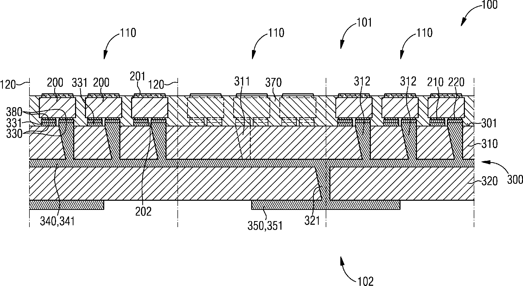
Im in
Die einzelnen Leuchtdiodenchips
Jeder der Leuchtdiodenchips
An der Kontaktseite
Die Leuchtdiodenchips
Die mehrlagige Leiterplatte
An der den Leuchtdiodenchips
Die Unterseite der zweiten Leiterplattenlage
Abschnitte der ersten Metallisierungslage
Die Metallisierungslagen
Im einfachsten Fall fallen die logischen Zeilen
In der Kreuzmatrix-Verschaltung
Die Kreuzmatrix-Verschaltung
Die erste Metallisierungslage
Die Leiterplatte
Die Leiterplatte
Die zweite Metallisierungslage
Die Zeilenleitungen
Die zweite Metallisierungslage
Jede Spaltenanschlussstruktur
Jede Zeilenanschlussstruktur
Die Anzahl der in der dritten Metallisierungslage
Jede in der dritten Metallisierungslage
Die Leiterplatte
Anschließend werden die vorproduzierten Leuchtdiodenchips
Die Kontaktelektroden
Um das Risiko eines Kurzschlusses zwischen den ersten Kontaktelektroden
Anschließend wird jeder Leuchtdiodenchip
Die Leuchtdiodenchips
Eine alternative Möglichkeit zur Reduzierung des Risikos eines Kurzschlusses zwischen den Kontaktelektroden
Nach dem Anordnen der Leuchtdiodenchips
Das Vergussmaterial
Das Vergussmaterial
Bei der in
An der von der zweiten Leiterplattenlage
In der dritten Leiterplattenlage
Die in der dritten Leiterplattenlage
In weiteren Ausführungsformen des Videowand-Moduls
Die Erfindung wurde anhand der bevorzugten Ausführungsbeispiele näher illustriert und beschrieben. Dennoch ist die Erfindung nicht auf die offenbarten Beispiele eingeschränkt. Vielmehr können hieraus andere Variationen vom Fachmann abgeleitet werden, ohne den Schutzumfang der Erfindung zu verlassen.The invention has been further illustrated and described with reference to the preferred embodiments. However, the invention is not limited to the disclosed examples. Rather, other variations may be deduced therefrom by those skilled in the art without departing from the scope of the invention.
BezugszeichenlisteLIST OF REFERENCE NUMBERS
- 100100
- Videowand-Modul Video Wall module
- 101101
- Vorderseite front
- 102102
- Rückseite back
- 110110
- Bildpunkt pixel
- 120120
- Rechteckgitter rectangular grid
- 121121
- Zeile von Bildpunkten Line of pixels
- 122122
- Spalte von Bildpunkten Column of pixels
- 130130
- Block (aus vier Bildpunkten) Block (from four pixels)
- 140140
- Kreuzmatrix-Verschaltung Cross matrix configuration
- 141141
- logische Zeile logical line
- 142142
- logische Spalte logical column
- 200200
- Leuchtdiodenchip LED chip
- 201201
- Strahlungsemissionsseite Radiation emission side
- 202202
- Kontaktseite Contact
- 210210
- erste Kontaktelektrode first contact electrode
- 220220
- zweite Kontaktelektrode second contact electrode
- 300300
- Leiterplatte circuit board
- 301301
- Oberseite top
- 310310
- erste Leiterplattenlage first circuit board position
- 311311
- erste obere Durchkontakte first upper vias
- 312312
- zweite obere Durchkontakte second upper vias
- 320320
- zweite Leiterplattenlage second circuit board position
- 321321
- untere Durchkontakte lower vias
- 330330
- erste Metallisierungslage first metallization layer
- 331331
- Spaltenleitung column line
- 340340
- zweite Metallisierungslage second metallization layer
- 341341
- Zeilenleitung row line
- 342342
- Zeilenanschlussstruktur Lines connecting structure
- 343343
- Spaltenanschlussstruktur Column connection structure
- 350350
- dritte Metallisierungslage third metallization layer
- 351351
- elektrische Kontaktfläche electrical contact surface
- 360360
- dritte Leiterplattenlage third circuit board position
- 361361
- elektronisches Bauelement electronic component
- 370370
- Vergussmaterial grout
- 380380
- Conductive-Die-Attach-Film Conductive die attach film
- 390390
- anisotrop leitende Folie anisotropically conductive film
- 400400
- vierte Metallisierungslage fourth metallization situation
- 401401
- elektrische Kontaktfläche electrical contact surface
Claims (18)
Priority Applications (7)
| Application Number | Priority Date | Filing Date | Title |
|---|---|---|---|
| DE102016103324.3A DE102016103324A1 (en) | 2016-02-25 | 2016-02-25 | Video wall module and method of making a video wall module |
| JP2018541249A JP6653022B2 (en) | 2016-02-25 | 2017-02-24 | Video wall module and method of manufacturing video wall module |
| DE112017000995.2T DE112017000995A5 (en) | 2016-02-25 | 2017-02-24 | Video wall module and method of making a video wall module |
| PCT/EP2017/054299 WO2017144650A1 (en) | 2016-02-25 | 2017-02-24 | Video wall module and method for producing a video wall module |
| US16/079,370 US10797026B2 (en) | 2016-02-25 | 2017-02-24 | Video wall module and method of producing a video wall module |
| KR1020187024019A KR102693153B1 (en) | 2016-02-25 | 2017-02-24 | Video wall module and method for manufacturing video wall module |
| CN201780013235.6A CN108701434B (en) | 2016-02-25 | 2017-02-24 | Video wall module and method for producing a video wall module |
Applications Claiming Priority (1)
| Application Number | Priority Date | Filing Date | Title |
|---|---|---|---|
| DE102016103324.3A DE102016103324A1 (en) | 2016-02-25 | 2016-02-25 | Video wall module and method of making a video wall module |
Publications (1)
| Publication Number | Publication Date |
|---|---|
| DE102016103324A1 true DE102016103324A1 (en) | 2017-08-31 |
Family
ID=58228092
Family Applications (2)
| Application Number | Title | Priority Date | Filing Date |
|---|---|---|---|
| DE102016103324.3A Withdrawn DE102016103324A1 (en) | 2016-02-25 | 2016-02-25 | Video wall module and method of making a video wall module |
| DE112017000995.2T Pending DE112017000995A5 (en) | 2016-02-25 | 2017-02-24 | Video wall module and method of making a video wall module |
Family Applications After (1)
| Application Number | Title | Priority Date | Filing Date |
|---|---|---|---|
| DE112017000995.2T Pending DE112017000995A5 (en) | 2016-02-25 | 2017-02-24 | Video wall module and method of making a video wall module |
Country Status (6)
| Country | Link |
|---|---|
| US (1) | US10797026B2 (en) |
| JP (1) | JP6653022B2 (en) |
| KR (1) | KR102693153B1 (en) |
| CN (1) | CN108701434B (en) |
| DE (2) | DE102016103324A1 (en) |
| WO (1) | WO2017144650A1 (en) |
Cited By (1)
| Publication number | Priority date | Publication date | Assignee | Title |
|---|---|---|---|---|
| EP4040481A1 (en) * | 2021-02-09 | 2022-08-10 | InnoLux Corporation | Electronic device |
Families Citing this family (8)
| Publication number | Priority date | Publication date | Assignee | Title |
|---|---|---|---|---|
| JP6411685B1 (en) * | 2017-10-12 | 2018-10-24 | ルーメンス カンパニー リミテッド | LED module assembly for display |
| US10707190B2 (en) * | 2018-04-10 | 2020-07-07 | Glo Ab | LED backplane having planar bonding surfaces and method of making thereof |
| JP7267683B2 (en) * | 2018-04-25 | 2023-05-02 | シャープ株式会社 | Light-emitting element module |
| DE102019106546A1 (en) * | 2019-03-14 | 2020-09-17 | OSRAM Opto Semiconductors Gesellschaft mit beschränkter Haftung | METHOD FOR MANUFACTURING OPTOELECTRONIC SEMICONDUCTOR COMPONENTS AND OPTOELECTRONIC SEMICONDUCTOR COMPONENTS |
| WO2020237629A1 (en) | 2019-05-31 | 2020-12-03 | 京东方科技集团股份有限公司 | Display back plate and manufacturing method, display panel and manufacturing method, and display device |
| EP3979317B1 (en) | 2019-05-31 | 2024-11-06 | BOE Technology Group Co., Ltd. | Display backplane and manufacturing method therefor, and display device |
| TWI757996B (en) | 2020-08-24 | 2022-03-11 | 錼創顯示科技股份有限公司 | Micro light emitting diode display matrix module |
| CN115224181B (en) * | 2021-04-20 | 2025-08-22 | 群创光电股份有限公司 | Light-emitting module and light-emitting device including the same |
Citations (1)
| Publication number | Priority date | Publication date | Assignee | Title |
|---|---|---|---|---|
| DE102015100294A1 (en) * | 2014-01-13 | 2015-07-16 | Samsung Electronics Co., Ltd. | Light-emitting semiconductor device |
Family Cites Families (23)
| Publication number | Priority date | Publication date | Assignee | Title |
|---|---|---|---|---|
| US6370019B1 (en) * | 1998-02-17 | 2002-04-09 | Sarnoff Corporation | Sealing of large area display structures |
| US20030058650A1 (en) * | 2001-09-25 | 2003-03-27 | Kelvin Shih | Light emitting diode with integrated heat dissipater |
| EP1469450A1 (en) * | 2003-04-18 | 2004-10-20 | Barco N.V. | Organic light-emitting diode display assembly for use in a large-screen display |
| EP1501069B1 (en) * | 2003-07-22 | 2005-11-09 | Barco N.V. | Method for controlling an organic light-emitting diode display, and display arranged to apply this method |
| EP1548573A1 (en) | 2003-12-23 | 2005-06-29 | Barco N.V. | Hierarchical control system for a tiled large-screen emissive display |
| DE102006028692B4 (en) | 2006-05-19 | 2021-09-02 | OSRAM Opto Semiconductors Gesellschaft mit beschränkter Haftung | Electrically conductive connection with an insulating connection medium |
| TWI528514B (en) * | 2009-08-20 | 2016-04-01 | 精材科技股份有限公司 | Chip package and method of manufacturing same |
| US8642448B2 (en) | 2010-06-22 | 2014-02-04 | Applied Materials, Inc. | Wafer dicing using femtosecond-based laser and plasma etch |
| US20130100694A1 (en) * | 2011-10-24 | 2013-04-25 | Kocam International Co., Ltd. | LED Backlight Module |
| US8794501B2 (en) * | 2011-11-18 | 2014-08-05 | LuxVue Technology Corporation | Method of transferring a light emitting diode |
| EP2731126A1 (en) * | 2012-11-09 | 2014-05-14 | Nederlandse Organisatie voor toegepast -natuurwetenschappelijk onderzoek TNO | Method for bonding bare chip dies |
| TWI505002B (en) * | 2013-02-05 | 2015-10-21 | 隆達電子股份有限公司 | LED display panel |
| US9111464B2 (en) * | 2013-06-18 | 2015-08-18 | LuxVue Technology Corporation | LED display with wavelength conversion layer |
| KR101513641B1 (en) * | 2013-08-20 | 2015-04-22 | 엘지전자 주식회사 | Display |
| KR101521939B1 (en) * | 2013-12-17 | 2015-05-20 | 엘지전자 주식회사 | Display device using semiconductor light emitting device and method of fabricating the same |
| JP2015197544A (en) | 2014-03-31 | 2015-11-09 | ソニー株式会社 | Mounting board and electronic equipment |
| CN113035850B (en) * | 2014-06-18 | 2022-12-06 | 艾克斯展示公司技术有限公司 | Micro-assembly LED display |
| US20160004123A1 (en) * | 2014-07-02 | 2016-01-07 | Kabushiki Kaisha Toshiba | Image display apparatus |
| JP2016018877A (en) | 2014-07-08 | 2016-02-01 | 三菱電機株式会社 | Dicing tape and manufacturing method thereof |
| US9818725B2 (en) * | 2015-06-01 | 2017-11-14 | X-Celeprint Limited | Inorganic-light-emitter display with integrated black matrix |
| US9941450B2 (en) * | 2015-06-18 | 2018-04-10 | Articulated Technologies, Llc | Roll-to-roll fabricated light sheet and encapsulated semiconductor device |
| DE102015112556B4 (en) * | 2015-07-30 | 2024-03-21 | OSRAM Opto Semiconductors Gesellschaft mit beschränkter Haftung | Video wall module and method for producing the same |
| US10177016B2 (en) * | 2015-08-18 | 2019-01-08 | Goertek Inc. | Pre-screening method, manufacturing method, device and electronic apparatus of micro-LED |
-
2016
- 2016-02-25 DE DE102016103324.3A patent/DE102016103324A1/en not_active Withdrawn
-
2017
- 2017-02-24 JP JP2018541249A patent/JP6653022B2/en active Active
- 2017-02-24 WO PCT/EP2017/054299 patent/WO2017144650A1/en not_active Ceased
- 2017-02-24 KR KR1020187024019A patent/KR102693153B1/en active Active
- 2017-02-24 DE DE112017000995.2T patent/DE112017000995A5/en active Pending
- 2017-02-24 US US16/079,370 patent/US10797026B2/en active Active
- 2017-02-24 CN CN201780013235.6A patent/CN108701434B/en active Active
Patent Citations (1)
| Publication number | Priority date | Publication date | Assignee | Title |
|---|---|---|---|---|
| DE102015100294A1 (en) * | 2014-01-13 | 2015-07-16 | Samsung Electronics Co., Ltd. | Light-emitting semiconductor device |
Cited By (1)
| Publication number | Priority date | Publication date | Assignee | Title |
|---|---|---|---|---|
| EP4040481A1 (en) * | 2021-02-09 | 2022-08-10 | InnoLux Corporation | Electronic device |
Also Published As
| Publication number | Publication date |
|---|---|
| US10797026B2 (en) | 2020-10-06 |
| US20190057955A1 (en) | 2019-02-21 |
| CN108701434B (en) | 2021-12-24 |
| KR20180115272A (en) | 2018-10-22 |
| WO2017144650A1 (en) | 2017-08-31 |
| CN108701434A (en) | 2018-10-23 |
| JP2019507904A (en) | 2019-03-22 |
| JP6653022B2 (en) | 2020-02-26 |
| DE112017000995A5 (en) | 2018-11-22 |
| KR102693153B1 (en) | 2024-08-09 |
Similar Documents
| Publication | Publication Date | Title |
|---|---|---|
| DE102016103324A1 (en) | Video wall module and method of making a video wall module | |
| DE112019004015B4 (en) | Optoelectronic semiconductor component and manufacturing method for optoelectronic semiconductor components | |
| WO2020030550A1 (en) | Lighting device | |
| EP0878026B1 (en) | Led matrix | |
| DE102014116133B4 (en) | Optoelectronic component, method for producing an optoelectronic component and method for producing an optoelectronic arrangement | |
| DE102016208431A1 (en) | Arrangement with an electrical component | |
| EP3360167B1 (en) | Optoelectronic component having a lead frame having a stiffening structure | |
| DE102017123290A1 (en) | Light-emitting component, display device and method for producing a display device | |
| WO2018002321A1 (en) | Modular module | |
| DE102015118433A1 (en) | Optoelectronic component and method for its production | |
| WO2016150841A1 (en) | Optoelectronic component and method for producing same | |
| EP2332186A1 (en) | Led module and production method | |
| DE102015112556B4 (en) | Video wall module and method for producing the same | |
| WO2019002098A1 (en) | OPTOELECTRONIC SEMICONDUCTOR COMPONENT AND ARRANGEMENT WITH AN OPTOELECTRONIC SEMICONDUCTOR COMPONENT | |
| EP3262627B1 (en) | Light-emitting diode apparatus and method for manufacturing a light-emitting diode apparatus | |
| DE112020004819B4 (en) | Display device and display unit | |
| DE112014001166B4 (en) | Optoelectronic component and electronic device with optoelectronic component | |
| DE102014117897A1 (en) | Method for producing optoelectronic modules and arrangement with such a module | |
| WO2020038777A1 (en) | Printed circuit board, and method for producing a printed circuit board having at least one optoelectronic component integrated into the printed circuit board | |
| DE102014208960A1 (en) | Surface-mountable optoelectronic component and method for producing a surface-mountable optoelectronic component | |
| WO2024260997A1 (en) | Laser package and laser device comprising laser packages | |
| DE102023134389A1 (en) | OPTOELECTRONIC COMPONENT | |
| DE102016103328A1 (en) | Method for producing an optoelectronic component and optoelectronic component | |
| WO2018024705A1 (en) | Multi-chip module | |
| WO2018015274A1 (en) | Module for a video wall, and method for producing same |
Legal Events
| Date | Code | Title | Description |
|---|---|---|---|
| R079 | Amendment of ipc main class |
Free format text: PREVIOUS MAIN CLASS: H01L0025075000 Ipc: G09F0009330000 |
|
| R163 | Identified publications notified | ||
| R118 | Application deemed withdrawn due to claim for domestic priority |