DE102015112412A1 - The color non-altering multi-layer structures and protective coating thereon - Google Patents
The color non-altering multi-layer structures and protective coating thereon Download PDFInfo
- Publication number
- DE102015112412A1 DE102015112412A1 DE102015112412.2A DE102015112412A DE102015112412A1 DE 102015112412 A1 DE102015112412 A1 DE 102015112412A1 DE 102015112412 A DE102015112412 A DE 102015112412A DE 102015112412 A1 DE102015112412 A1 DE 102015112412A1
- Authority
- DE
- Germany
- Prior art keywords
- layer
- pigment
- omnidirectional
- oxide layer
- electromagnetic radiation
- Prior art date
- Legal status (The legal status is an assumption and is not a legal conclusion. Google has not performed a legal analysis and makes no representation as to the accuracy of the status listed.)
- Pending
Links
- 239000011253 protective coating Substances 0.000 title claims abstract description 29
- 239000000049 pigment Substances 0.000 claims abstract description 139
- 230000005670 electromagnetic radiation Effects 0.000 claims abstract description 72
- 239000000463 material Substances 0.000 claims abstract description 31
- 238000000576 coating method Methods 0.000 claims abstract description 24
- 239000011248 coating agent Substances 0.000 claims abstract description 22
- 230000001699 photocatalysis Effects 0.000 claims abstract description 15
- VYPSYNLAJGMNEJ-UHFFFAOYSA-N Silicium dioxide Chemical group O=[Si]=O VYPSYNLAJGMNEJ-UHFFFAOYSA-N 0.000 claims description 63
- 239000000377 silicon dioxide Substances 0.000 claims description 27
- PNEYBMLMFCGWSK-UHFFFAOYSA-N aluminium oxide Inorganic materials [O-2].[O-2].[O-2].[Al+3].[Al+3] PNEYBMLMFCGWSK-UHFFFAOYSA-N 0.000 claims description 22
- GWEVSGVZZGPLCZ-UHFFFAOYSA-N Titan oxide Chemical compound O=[Ti]=O GWEVSGVZZGPLCZ-UHFFFAOYSA-N 0.000 claims description 15
- MCMNRKCIXSYSNV-UHFFFAOYSA-N Zirconium dioxide Chemical compound O=[Zr]=O MCMNRKCIXSYSNV-UHFFFAOYSA-N 0.000 claims description 14
- CETPSERCERDGAM-UHFFFAOYSA-N ceric oxide Chemical compound O=[Ce]=O CETPSERCERDGAM-UHFFFAOYSA-N 0.000 claims description 13
- 229910000422 cerium(IV) oxide Inorganic materials 0.000 claims description 13
- 229910052814 silicon oxide Inorganic materials 0.000 claims description 3
- 239000010410 layer Substances 0.000 description 335
- KFZMGEQAYNKOFK-UHFFFAOYSA-N Isopropanol Chemical compound CC(C)O KFZMGEQAYNKOFK-UHFFFAOYSA-N 0.000 description 60
- LFQSCWFLJHTTHZ-UHFFFAOYSA-N Ethanol Chemical compound CCO LFQSCWFLJHTTHZ-UHFFFAOYSA-N 0.000 description 49
- 239000000243 solution Substances 0.000 description 36
- 229910004298 SiO 2 Inorganic materials 0.000 description 33
- 239000010409 thin film Substances 0.000 description 33
- 229910052984 zinc sulfide Inorganic materials 0.000 description 31
- 239000011651 chromium Substances 0.000 description 29
- 239000005083 Zinc sulfide Substances 0.000 description 26
- 239000006096 absorbing agent Substances 0.000 description 25
- 239000002245 particle Substances 0.000 description 25
- 239000000725 suspension Substances 0.000 description 24
- XLYOFNOQVPJJNP-UHFFFAOYSA-N water Substances O XLYOFNOQVPJJNP-UHFFFAOYSA-N 0.000 description 23
- HEMHJVSKTPXQMS-UHFFFAOYSA-M Sodium hydroxide Chemical compound [OH-].[Na+] HEMHJVSKTPXQMS-UHFFFAOYSA-M 0.000 description 21
- 229910052681 coesite Inorganic materials 0.000 description 20
- 229910052906 cristobalite Inorganic materials 0.000 description 20
- 230000005684 electric field Effects 0.000 description 20
- 235000012239 silicon dioxide Nutrition 0.000 description 20
- 229910052682 stishovite Inorganic materials 0.000 description 20
- 229910052905 tridymite Inorganic materials 0.000 description 20
- 239000002250 absorbent Substances 0.000 description 19
- 230000002745 absorbent Effects 0.000 description 19
- 238000013461 design Methods 0.000 description 19
- 229910018072 Al 2 O 3 Inorganic materials 0.000 description 18
- 239000007787 solid Substances 0.000 description 17
- 239000000203 mixture Substances 0.000 description 15
- 229910052593 corundum Inorganic materials 0.000 description 13
- 238000000034 method Methods 0.000 description 13
- 229910001845 yogo sapphire Inorganic materials 0.000 description 13
- -1 Ti-nitride Substances 0.000 description 11
- NBIIXXVUZAFLBC-UHFFFAOYSA-N Phosphoric acid Chemical compound OP(O)(O)=O NBIIXXVUZAFLBC-UHFFFAOYSA-N 0.000 description 10
- 239000007788 liquid Substances 0.000 description 10
- 239000011247 coating layer Substances 0.000 description 9
- 238000006073 displacement reaction Methods 0.000 description 9
- 239000003973 paint Substances 0.000 description 9
- 238000003756 stirring Methods 0.000 description 9
- 229910052782 aluminium Inorganic materials 0.000 description 8
- 239000003989 dielectric material Substances 0.000 description 8
- 239000010445 mica Substances 0.000 description 8
- 229910052618 mica group Inorganic materials 0.000 description 8
- 239000002002 slurry Substances 0.000 description 8
- 238000004448 titration Methods 0.000 description 8
- 238000010521 absorption reaction Methods 0.000 description 7
- CSCPPACGZOOCGX-UHFFFAOYSA-N Acetone Chemical compound CC(C)=O CSCPPACGZOOCGX-UHFFFAOYSA-N 0.000 description 6
- LYCAIKOWRPUZTN-UHFFFAOYSA-N Ethylene glycol Chemical compound OCCO LYCAIKOWRPUZTN-UHFFFAOYSA-N 0.000 description 6
- 229910010413 TiO 2 Inorganic materials 0.000 description 6
- XAGFODPZIPBFFR-UHFFFAOYSA-N aluminium Chemical compound [Al] XAGFODPZIPBFFR-UHFFFAOYSA-N 0.000 description 6
- BSDOQSMQCZQLDV-UHFFFAOYSA-N butan-1-olate;zirconium(4+) Chemical compound [Zr+4].CCCC[O-].CCCC[O-].CCCC[O-].CCCC[O-] BSDOQSMQCZQLDV-UHFFFAOYSA-N 0.000 description 6
- 239000010949 copper Substances 0.000 description 6
- 238000004519 manufacturing process Methods 0.000 description 6
- 229910052751 metal Inorganic materials 0.000 description 6
- 239000002184 metal Substances 0.000 description 6
- 229910052710 silicon Inorganic materials 0.000 description 6
- 238000001228 spectrum Methods 0.000 description 6
- 238000001429 visible spectrum Methods 0.000 description 6
- LRHPLDYGYMQRHN-UHFFFAOYSA-N N-Butanol Chemical compound CCCCO LRHPLDYGYMQRHN-UHFFFAOYSA-N 0.000 description 5
- 239000004698 Polyethylene Substances 0.000 description 5
- 229910000147 aluminium phosphate Inorganic materials 0.000 description 5
- 230000005540 biological transmission Effects 0.000 description 5
- PQXKHYXIUOZZFA-UHFFFAOYSA-M lithium fluoride Chemical compound [Li+].[F-] PQXKHYXIUOZZFA-UHFFFAOYSA-M 0.000 description 5
- 239000003960 organic solvent Substances 0.000 description 5
- 150000001282 organosilanes Chemical class 0.000 description 5
- RVTZCBVAJQQJTK-UHFFFAOYSA-N oxygen(2-);zirconium(4+) Chemical compound [O-2].[O-2].[Zr+4] RVTZCBVAJQQJTK-UHFFFAOYSA-N 0.000 description 5
- 229920000573 polyethylene Polymers 0.000 description 5
- WOZZOSDBXABUFO-UHFFFAOYSA-N tri(butan-2-yloxy)alumane Chemical compound [Al+3].CCC(C)[O-].CCC(C)[O-].CCC(C)[O-] WOZZOSDBXABUFO-UHFFFAOYSA-N 0.000 description 5
- 229910001928 zirconium oxide Inorganic materials 0.000 description 5
- XUIMIQQOPSSXEZ-UHFFFAOYSA-N Silicon Chemical compound [Si] XUIMIQQOPSSXEZ-UHFFFAOYSA-N 0.000 description 4
- 230000004888 barrier function Effects 0.000 description 4
- 230000008859 change Effects 0.000 description 4
- URLJKFSTXLNXLG-UHFFFAOYSA-N niobium(5+);oxygen(2-) Chemical compound [O-2].[O-2].[O-2].[O-2].[O-2].[Nb+5].[Nb+5] URLJKFSTXLNXLG-UHFFFAOYSA-N 0.000 description 4
- 239000010703 silicon Substances 0.000 description 4
- 238000004088 simulation Methods 0.000 description 4
- 229910052719 titanium Inorganic materials 0.000 description 4
- 239000010936 titanium Substances 0.000 description 4
- 229910052726 zirconium Inorganic materials 0.000 description 4
- QTBSBXVTEAMEQO-UHFFFAOYSA-N Acetic acid Chemical compound CC(O)=O QTBSBXVTEAMEQO-UHFFFAOYSA-N 0.000 description 3
- VYZAMTAEIAYCRO-UHFFFAOYSA-N Chromium Chemical compound [Cr] VYZAMTAEIAYCRO-UHFFFAOYSA-N 0.000 description 3
- PIICEJLVQHRZGT-UHFFFAOYSA-N Ethylenediamine Chemical compound NCCN PIICEJLVQHRZGT-UHFFFAOYSA-N 0.000 description 3
- 239000004793 Polystyrene Substances 0.000 description 3
- BOTDANWDWHJENH-UHFFFAOYSA-N Tetraethyl orthosilicate Chemical compound CCO[Si](OCC)(OCC)OCC BOTDANWDWHJENH-UHFFFAOYSA-N 0.000 description 3
- RTAQQCXQSZGOHL-UHFFFAOYSA-N Titanium Chemical compound [Ti] RTAQQCXQSZGOHL-UHFFFAOYSA-N 0.000 description 3
- QCWXUUIWCKQGHC-UHFFFAOYSA-N Zirconium Chemical compound [Zr] QCWXUUIWCKQGHC-UHFFFAOYSA-N 0.000 description 3
- 229910045601 alloy Inorganic materials 0.000 description 3
- 239000000956 alloy Substances 0.000 description 3
- 238000013459 approach Methods 0.000 description 3
- 238000004364 calculation method Methods 0.000 description 3
- 229910052804 chromium Inorganic materials 0.000 description 3
- 229910052802 copper Inorganic materials 0.000 description 3
- 239000012792 core layer Substances 0.000 description 3
- 238000010586 diagram Methods 0.000 description 3
- 229910052737 gold Inorganic materials 0.000 description 3
- 239000010931 gold Substances 0.000 description 3
- 239000000976 ink Substances 0.000 description 3
- 230000003287 optical effect Effects 0.000 description 3
- 229920002223 polystyrene Polymers 0.000 description 3
- 239000002243 precursor Substances 0.000 description 3
- 230000008569 process Effects 0.000 description 3
- 238000012545 processing Methods 0.000 description 3
- 238000010992 reflux Methods 0.000 description 3
- LIVNPJMFVYWSIS-UHFFFAOYSA-N silicon monoxide Chemical compound [Si-]#[O+] LIVNPJMFVYWSIS-UHFFFAOYSA-N 0.000 description 3
- 239000011734 sodium Substances 0.000 description 3
- 229910052725 zinc Inorganic materials 0.000 description 3
- 239000011701 zinc Substances 0.000 description 3
- SKJCKYVIQGBWTN-UHFFFAOYSA-N (4-hydroxyphenyl) methanesulfonate Chemical compound CS(=O)(=O)OC1=CC=C(O)C=C1 SKJCKYVIQGBWTN-UHFFFAOYSA-N 0.000 description 2
- PFNQVRZLDWYSCW-UHFFFAOYSA-N (fluoren-9-ylideneamino) n-naphthalen-1-ylcarbamate Chemical compound C12=CC=CC=C2C2=CC=CC=C2C1=NOC(=O)NC1=CC=CC2=CC=CC=C12 PFNQVRZLDWYSCW-UHFFFAOYSA-N 0.000 description 2
- XDLMVUHYZWKMMD-UHFFFAOYSA-N 3-trimethoxysilylpropyl 2-methylprop-2-enoate Chemical compound CO[Si](OC)(OC)CCCOC(=O)C(C)=C XDLMVUHYZWKMMD-UHFFFAOYSA-N 0.000 description 2
- NLXLAEXVIDQMFP-UHFFFAOYSA-N Ammonium chloride Substances [NH4+].[Cl-] NLXLAEXVIDQMFP-UHFFFAOYSA-N 0.000 description 2
- VHUUQVKOLVNVRT-UHFFFAOYSA-N Ammonium hydroxide Chemical compound [NH4+].[OH-] VHUUQVKOLVNVRT-UHFFFAOYSA-N 0.000 description 2
- OKTJSMMVPCPJKN-UHFFFAOYSA-N Carbon Chemical compound [C] OKTJSMMVPCPJKN-UHFFFAOYSA-N 0.000 description 2
- 229910004631 Ce(NO3)3.6H2O Inorganic materials 0.000 description 2
- 229910052684 Cerium Inorganic materials 0.000 description 2
- GYHNNYVSQQEPJS-UHFFFAOYSA-N Gallium Chemical compound [Ga] GYHNNYVSQQEPJS-UHFFFAOYSA-N 0.000 description 2
- 239000004962 Polyamide-imide Substances 0.000 description 2
- 229910052581 Si3N4 Inorganic materials 0.000 description 2
- CBIFDJDRCNEMQB-UHFFFAOYSA-N [Al].O[As](O)(O)=O Chemical compound [Al].O[As](O)(O)=O CBIFDJDRCNEMQB-UHFFFAOYSA-N 0.000 description 2
- 239000003929 acidic solution Substances 0.000 description 2
- QGZKDVFQNNGYKY-UHFFFAOYSA-N ammonia Natural products N QGZKDVFQNNGYKY-UHFFFAOYSA-N 0.000 description 2
- 235000011114 ammonium hydroxide Nutrition 0.000 description 2
- OYLGJCQECKOTOL-UHFFFAOYSA-L barium fluoride Chemical compound [F-].[F-].[Ba+2] OYLGJCQECKOTOL-UHFFFAOYSA-L 0.000 description 2
- 229910001632 barium fluoride Inorganic materials 0.000 description 2
- GWXLDORMOJMVQZ-UHFFFAOYSA-N cerium Chemical compound [Ce] GWXLDORMOJMVQZ-UHFFFAOYSA-N 0.000 description 2
- 239000005387 chalcogenide glass Substances 0.000 description 2
- 238000012512 characterization method Methods 0.000 description 2
- UUAGAQFQZIEFAH-UHFFFAOYSA-N chlorotrifluoroethylene Chemical group FC(F)=C(F)Cl UUAGAQFQZIEFAH-UHFFFAOYSA-N 0.000 description 2
- 230000001419 dependent effect Effects 0.000 description 2
- 238000000151 deposition Methods 0.000 description 2
- 230000008021 deposition Effects 0.000 description 2
- BUACSMWVFUNQET-UHFFFAOYSA-H dialuminum;trisulfate;hydrate Chemical compound O.[Al+3].[Al+3].[O-]S([O-])(=O)=O.[O-]S([O-])(=O)=O.[O-]S([O-])(=O)=O BUACSMWVFUNQET-UHFFFAOYSA-H 0.000 description 2
- NBVXSUQYWXRMNV-UHFFFAOYSA-N fluoromethane Chemical compound FC NBVXSUQYWXRMNV-UHFFFAOYSA-N 0.000 description 2
- 229910052733 gallium Inorganic materials 0.000 description 2
- 229910000154 gallium phosphate Inorganic materials 0.000 description 2
- LWFNJDOYCSNXDO-UHFFFAOYSA-K gallium;phosphate Chemical compound [Ga+3].[O-]P([O-])([O-])=O LWFNJDOYCSNXDO-UHFFFAOYSA-K 0.000 description 2
- 229910052732 germanium Inorganic materials 0.000 description 2
- CJNBYAVZURUTKZ-UHFFFAOYSA-N hafnium(iv) oxide Chemical compound O=[Hf]=O CJNBYAVZURUTKZ-UHFFFAOYSA-N 0.000 description 2
- UJXZVRRCKFUQKG-UHFFFAOYSA-K indium(3+);phosphate Chemical compound [In+3].[O-]P([O-])([O-])=O UJXZVRRCKFUQKG-UHFFFAOYSA-K 0.000 description 2
- 238000002329 infrared spectrum Methods 0.000 description 2
- 239000011572 manganese Substances 0.000 description 2
- PHQOGHDTIVQXHL-UHFFFAOYSA-N n'-(3-trimethoxysilylpropyl)ethane-1,2-diamine Chemical compound CO[Si](OC)(OC)CCCNCCN PHQOGHDTIVQXHL-UHFFFAOYSA-N 0.000 description 2
- ZKATWMILCYLAPD-UHFFFAOYSA-N niobium pentoxide Inorganic materials O=[Nb](=O)O[Nb](=O)=O ZKATWMILCYLAPD-UHFFFAOYSA-N 0.000 description 2
- 229920001778 nylon Polymers 0.000 description 2
- SIWVEOZUMHYXCS-UHFFFAOYSA-N oxo(oxoyttriooxy)yttrium Chemical compound O=[Y]O[Y]=O SIWVEOZUMHYXCS-UHFFFAOYSA-N 0.000 description 2
- 229920003229 poly(methyl methacrylate) Polymers 0.000 description 2
- 229920002312 polyamide-imide Polymers 0.000 description 2
- 229920001343 polytetrafluoroethylene Polymers 0.000 description 2
- 239000004810 polytetrafluoroethylene Substances 0.000 description 2
- 229910021426 porous silicon Inorganic materials 0.000 description 2
- BDERNNFJNOPAEC-UHFFFAOYSA-N propan-1-ol Chemical compound CCCO BDERNNFJNOPAEC-UHFFFAOYSA-N 0.000 description 2
- 239000011541 reaction mixture Substances 0.000 description 2
- 230000009467 reduction Effects 0.000 description 2
- 229920006395 saturated elastomer Polymers 0.000 description 2
- HQVNEWCFYHHQES-UHFFFAOYSA-N silicon nitride Chemical compound N12[Si]34N5[Si]62N3[Si]51N64 HQVNEWCFYHHQES-UHFFFAOYSA-N 0.000 description 2
- 239000002356 single layer Substances 0.000 description 2
- 238000003980 solgel method Methods 0.000 description 2
- FVRNDBHWWSPNOM-UHFFFAOYSA-L strontium fluoride Chemical compound [F-].[F-].[Sr+2] FVRNDBHWWSPNOM-UHFFFAOYSA-L 0.000 description 2
- 229910001637 strontium fluoride Inorganic materials 0.000 description 2
- 239000000758 substrate Substances 0.000 description 2
- 229910052718 tin Inorganic materials 0.000 description 2
- 239000011135 tin Substances 0.000 description 2
- XOLBLPGZBRYERU-UHFFFAOYSA-N tin dioxide Chemical compound O=[Sn]=O XOLBLPGZBRYERU-UHFFFAOYSA-N 0.000 description 2
- VXUYXOFXAQZZMF-UHFFFAOYSA-N titanium(IV) isopropoxide Chemical compound CC(C)O[Ti](OC(C)C)(OC(C)C)OC(C)C VXUYXOFXAQZZMF-UHFFFAOYSA-N 0.000 description 2
- 229910052721 tungsten Inorganic materials 0.000 description 2
- 238000002211 ultraviolet spectrum Methods 0.000 description 2
- DRDVZXDWVBGGMH-UHFFFAOYSA-N zinc;sulfide Chemical compound [S-2].[Zn+2] DRDVZXDWVBGGMH-UHFFFAOYSA-N 0.000 description 2
- 125000001637 1-naphthyl group Chemical group [H]C1=C([H])C([H])=C2C(*)=C([H])C([H])=C([H])C2=C1[H] 0.000 description 1
- JMMZCWZIJXAGKW-UHFFFAOYSA-N 2-methylpent-2-ene Chemical compound CCC=C(C)C JMMZCWZIJXAGKW-UHFFFAOYSA-N 0.000 description 1
- WXAIEIRYBSKHDP-UHFFFAOYSA-N 4-phenyl-n-(4-phenylphenyl)-n-[4-[4-(4-phenyl-n-(4-phenylphenyl)anilino)phenyl]phenyl]aniline Chemical compound C1=CC=CC=C1C1=CC=C(N(C=2C=CC(=CC=2)C=2C=CC=CC=2)C=2C=CC(=CC=2)C=2C=CC(=CC=2)N(C=2C=CC(=CC=2)C=2C=CC=CC=2)C=2C=CC(=CC=2)C=2C=CC=CC=2)C=C1 WXAIEIRYBSKHDP-UHFFFAOYSA-N 0.000 description 1
- RZVAJINKPMORJF-UHFFFAOYSA-N Acetaminophen Chemical compound CC(=O)NC1=CC=C(O)C=C1 RZVAJINKPMORJF-UHFFFAOYSA-N 0.000 description 1
- DJHGAFSJWGLOIV-UHFFFAOYSA-K Arsenate3- Chemical compound [O-][As]([O-])([O-])=O DJHGAFSJWGLOIV-UHFFFAOYSA-K 0.000 description 1
- 229910001369 Brass Inorganic materials 0.000 description 1
- 229910000906 Bronze Inorganic materials 0.000 description 1
- DQEFEBPAPFSJLV-UHFFFAOYSA-N Cellulose propionate Chemical compound CCC(=O)OCC1OC(OC(=O)CC)C(OC(=O)CC)C(OC(=O)CC)C1OC1C(OC(=O)CC)C(OC(=O)CC)C(OC(=O)CC)C(COC(=O)CC)O1 DQEFEBPAPFSJLV-UHFFFAOYSA-N 0.000 description 1
- RYGMFSIKBFXOCR-UHFFFAOYSA-N Copper Chemical compound [Cu] RYGMFSIKBFXOCR-UHFFFAOYSA-N 0.000 description 1
- 239000001856 Ethyl cellulose Substances 0.000 description 1
- ZZSNKZQZMQGXPY-UHFFFAOYSA-N Ethyl cellulose Chemical compound CCOCC1OC(OC)C(OCC)C(OCC)C1OC1C(O)C(O)C(OC)C(CO)O1 ZZSNKZQZMQGXPY-UHFFFAOYSA-N 0.000 description 1
- 229910005542 GaSb Inorganic materials 0.000 description 1
- JMASRVWKEDWRBT-UHFFFAOYSA-N Gallium nitride Chemical compound [Ga]#N JMASRVWKEDWRBT-UHFFFAOYSA-N 0.000 description 1
- PWHULOQIROXLJO-UHFFFAOYSA-N Manganese Chemical compound [Mn] PWHULOQIROXLJO-UHFFFAOYSA-N 0.000 description 1
- 239000000020 Nitrocellulose Substances 0.000 description 1
- 229920012266 Poly(ether sulfone) PES Polymers 0.000 description 1
- 239000004952 Polyamide Substances 0.000 description 1
- 239000004743 Polypropylene Substances 0.000 description 1
- 241000396922 Pontia daplidice Species 0.000 description 1
- 239000004115 Sodium Silicate Substances 0.000 description 1
- 239000002174 Styrene-butadiene Substances 0.000 description 1
- NRTOMJZYCJJWKI-UHFFFAOYSA-N Titanium nitride Chemical compound [Ti]#N NRTOMJZYCJJWKI-UHFFFAOYSA-N 0.000 description 1
- 229920001807 Urea-formaldehyde Polymers 0.000 description 1
- 241000404236 Zizina otis Species 0.000 description 1
- FJWGYAHXMCUOOM-QHOUIDNNSA-N [(2s,3r,4s,5r,6r)-2-[(2r,3r,4s,5r,6s)-4,5-dinitrooxy-2-(nitrooxymethyl)-6-[(2r,3r,4s,5r,6s)-4,5,6-trinitrooxy-2-(nitrooxymethyl)oxan-3-yl]oxyoxan-3-yl]oxy-3,5-dinitrooxy-6-(nitrooxymethyl)oxan-4-yl] nitrate Chemical compound O([C@@H]1O[C@@H]([C@H]([C@H](O[N+]([O-])=O)[C@H]1O[N+]([O-])=O)O[C@H]1[C@@H]([C@@H](O[N+]([O-])=O)[C@H](O[N+]([O-])=O)[C@@H](CO[N+]([O-])=O)O1)O[N+]([O-])=O)CO[N+](=O)[O-])[C@@H]1[C@@H](CO[N+]([O-])=O)O[C@@H](O[N+]([O-])=O)[C@H](O[N+]([O-])=O)[C@H]1O[N+]([O-])=O FJWGYAHXMCUOOM-QHOUIDNNSA-N 0.000 description 1
- NJSVDVPGINTNGX-UHFFFAOYSA-N [dimethoxy(propyl)silyl]oxymethanamine Chemical compound CCC[Si](OC)(OC)OCN NJSVDVPGINTNGX-UHFFFAOYSA-N 0.000 description 1
- 239000011358 absorbing material Substances 0.000 description 1
- 238000000862 absorption spectrum Methods 0.000 description 1
- DHKHKXVYLBGOIT-UHFFFAOYSA-N acetaldehyde Diethyl Acetal Natural products CCOC(C)OCC DHKHKXVYLBGOIT-UHFFFAOYSA-N 0.000 description 1
- 150000001241 acetals Chemical class 0.000 description 1
- 239000002253 acid Substances 0.000 description 1
- 150000007513 acids Chemical class 0.000 description 1
- NIXOWILDQLNWCW-UHFFFAOYSA-N acrylic acid group Chemical group C(C=C)(=O)O NIXOWILDQLNWCW-UHFFFAOYSA-N 0.000 description 1
- 229920006397 acrylic thermoplastic Polymers 0.000 description 1
- 239000004480 active ingredient Substances 0.000 description 1
- 230000032683 aging Effects 0.000 description 1
- DIZPMCHEQGEION-UHFFFAOYSA-H aluminium sulfate (anhydrous) Chemical compound [Al+3].[Al+3].[O-]S([O-])(=O)=O.[O-]S([O-])(=O)=O.[O-]S([O-])(=O)=O DIZPMCHEQGEION-UHFFFAOYSA-H 0.000 description 1
- ANBBXQWFNXMHLD-UHFFFAOYSA-N aluminum;sodium;oxygen(2-) Chemical compound [O-2].[O-2].[Na+].[Al+3] ANBBXQWFNXMHLD-UHFFFAOYSA-N 0.000 description 1
- 239000007864 aqueous solution Substances 0.000 description 1
- 229940000489 arsenate Drugs 0.000 description 1
- WBFMCDAQUDITAS-UHFFFAOYSA-N arsenic triselenide Chemical compound [Se]=[As][Se][As]=[Se] WBFMCDAQUDITAS-UHFFFAOYSA-N 0.000 description 1
- 239000010951 brass Substances 0.000 description 1
- 239000010974 bronze Substances 0.000 description 1
- MTAZNLWOLGHBHU-UHFFFAOYSA-N butadiene-styrene rubber Chemical compound C=CC=C.C=CC1=CC=CC=C1 MTAZNLWOLGHBHU-UHFFFAOYSA-N 0.000 description 1
- YHWCPXVTRSHPNY-UHFFFAOYSA-N butan-1-olate;titanium(4+) Chemical compound [Ti+4].CCCC[O-].CCCC[O-].CCCC[O-].CCCC[O-] YHWCPXVTRSHPNY-UHFFFAOYSA-N 0.000 description 1
- WUKWITHWXAAZEY-UHFFFAOYSA-L calcium difluoride Chemical compound [F-].[F-].[Ca+2] WUKWITHWXAAZEY-UHFFFAOYSA-L 0.000 description 1
- 229910001634 calcium fluoride Inorganic materials 0.000 description 1
- 229920002301 cellulose acetate Polymers 0.000 description 1
- 229920006217 cellulose acetate butyrate Polymers 0.000 description 1
- 229920006218 cellulose propionate Polymers 0.000 description 1
- 229910000420 cerium oxide Inorganic materials 0.000 description 1
- QQZMWMKOWKGPQY-UHFFFAOYSA-N cerium(3+);trinitrate;hexahydrate Chemical compound O.O.O.O.O.O.[Ce+3].[O-][N+]([O-])=O.[O-][N+]([O-])=O.[O-][N+]([O-])=O QQZMWMKOWKGPQY-UHFFFAOYSA-N 0.000 description 1
- VZDYWEUILIUIDF-UHFFFAOYSA-J cerium(4+);disulfate Chemical compound [Ce+4].[O-]S([O-])(=O)=O.[O-]S([O-])(=O)=O VZDYWEUILIUIDF-UHFFFAOYSA-J 0.000 description 1
- 229910000355 cerium(IV) sulfate Inorganic materials 0.000 description 1
- 238000006243 chemical reaction Methods 0.000 description 1
- 238000005229 chemical vapour deposition Methods 0.000 description 1
- KUNSUQLRTQLHQQ-UHFFFAOYSA-N copper tin Chemical compound [Cu].[Sn] KUNSUQLRTQLHQQ-UHFFFAOYSA-N 0.000 description 1
- 239000007822 coupling agent Substances 0.000 description 1
- 229910001610 cryolite Inorganic materials 0.000 description 1
- FPHIOHCCQGUGKU-UHFFFAOYSA-L difluorolead Chemical compound F[Pb]F FPHIOHCCQGUGKU-UHFFFAOYSA-L 0.000 description 1
- 239000006185 dispersion Substances 0.000 description 1
- 238000001035 drying Methods 0.000 description 1
- 238000000313 electron-beam-induced deposition Methods 0.000 description 1
- ZBQZBWKNGDEDOA-UHFFFAOYSA-N eosin B Chemical compound O1C(=O)C2=CC=CC=C2C21C1=CC([N+]([O-])=O)=C(O)C(Br)=C1OC1=C2C=C([N+]([O-])=O)C(O)=C1Br ZBQZBWKNGDEDOA-UHFFFAOYSA-N 0.000 description 1
- 229920001249 ethyl cellulose Polymers 0.000 description 1
- 235000019325 ethyl cellulose Nutrition 0.000 description 1
- 125000001495 ethyl group Chemical group [H]C([H])([H])C([H])([H])* 0.000 description 1
- 230000001747 exhibiting effect Effects 0.000 description 1
- 239000011888 foil Substances 0.000 description 1
- GNPVGFCGXDBREM-UHFFFAOYSA-N germanium atom Chemical compound [Ge] GNPVGFCGXDBREM-UHFFFAOYSA-N 0.000 description 1
- PCHJSUWPFVWCPO-UHFFFAOYSA-N gold Chemical compound [Au] PCHJSUWPFVWCPO-UHFFFAOYSA-N 0.000 description 1
- 239000010439 graphite Substances 0.000 description 1
- 229910002804 graphite Inorganic materials 0.000 description 1
- 229920001519 homopolymer Polymers 0.000 description 1
- 230000006872 improvement Effects 0.000 description 1
- RPQDHPTXJYYUPQ-UHFFFAOYSA-N indium arsenide Chemical compound [In]#[As] RPQDHPTXJYYUPQ-UHFFFAOYSA-N 0.000 description 1
- AMGQUBHHOARCQH-UHFFFAOYSA-N indium;oxotin Chemical compound [In].[Sn]=O AMGQUBHHOARCQH-UHFFFAOYSA-N 0.000 description 1
- 229920000554 ionomer Polymers 0.000 description 1
- XEEYBQQBJWHFJM-UHFFFAOYSA-N iron Substances [Fe] XEEYBQQBJWHFJM-UHFFFAOYSA-N 0.000 description 1
- UQSXHKLRYXJYBZ-UHFFFAOYSA-N iron oxide Inorganic materials [Fe]=O UQSXHKLRYXJYBZ-UHFFFAOYSA-N 0.000 description 1
- 235000013980 iron oxide Nutrition 0.000 description 1
- VBMVTYDPPZVILR-UHFFFAOYSA-N iron(2+);oxygen(2-) Chemical class [O-2].[Fe+2] VBMVTYDPPZVILR-UHFFFAOYSA-N 0.000 description 1
- ORUIBWPALBXDOA-UHFFFAOYSA-L magnesium fluoride Chemical compound [F-].[F-].[Mg+2] ORUIBWPALBXDOA-UHFFFAOYSA-L 0.000 description 1
- 229910052748 manganese Inorganic materials 0.000 description 1
- 239000011159 matrix material Substances 0.000 description 1
- 150000002739 metals Chemical class 0.000 description 1
- 238000012986 modification Methods 0.000 description 1
- 230000004048 modification Effects 0.000 description 1
- 229910052750 molybdenum Inorganic materials 0.000 description 1
- 239000002073 nanorod Substances 0.000 description 1
- 229910052759 nickel Inorganic materials 0.000 description 1
- 229910052758 niobium Inorganic materials 0.000 description 1
- 239000010955 niobium Substances 0.000 description 1
- 229910000484 niobium oxide Inorganic materials 0.000 description 1
- 229920001220 nitrocellulos Polymers 0.000 description 1
- 239000003921 oil Substances 0.000 description 1
- TWNQGVIAIRXVLR-UHFFFAOYSA-N oxo(oxoalumanyloxy)alumane Chemical compound O=[Al]O[Al]=O TWNQGVIAIRXVLR-UHFFFAOYSA-N 0.000 description 1
- BMMGVYCKOGBVEV-UHFFFAOYSA-N oxo(oxoceriooxy)cerium Chemical compound [Ce]=O.O=[Ce]=O BMMGVYCKOGBVEV-UHFFFAOYSA-N 0.000 description 1
- 229910052763 palladium Inorganic materials 0.000 description 1
- 239000013618 particulate matter Substances 0.000 description 1
- 238000005240 physical vapour deposition Methods 0.000 description 1
- 229910052697 platinum Inorganic materials 0.000 description 1
- BASFCYQUMIYNBI-UHFFFAOYSA-N platinum Substances [Pt] BASFCYQUMIYNBI-UHFFFAOYSA-N 0.000 description 1
- 239000002798 polar solvent Substances 0.000 description 1
- 229920002285 poly(styrene-co-acrylonitrile) Polymers 0.000 description 1
- 229920002492 poly(sulfone) Polymers 0.000 description 1
- 229920002647 polyamide Polymers 0.000 description 1
- 229920001748 polybutylene Polymers 0.000 description 1
- 229920000642 polymer Polymers 0.000 description 1
- 239000004926 polymethyl methacrylate Substances 0.000 description 1
- ODGAOXROABLFNM-UHFFFAOYSA-N polynoxylin Chemical compound O=C.NC(N)=O ODGAOXROABLFNM-UHFFFAOYSA-N 0.000 description 1
- 229920001155 polypropylene Polymers 0.000 description 1
- NROKBHXJSPEDAR-UHFFFAOYSA-M potassium fluoride Chemical compound [F-].[K+] NROKBHXJSPEDAR-UHFFFAOYSA-M 0.000 description 1
- 230000000135 prohibitive effect Effects 0.000 description 1
- 230000001681 protective effect Effects 0.000 description 1
- 239000011241 protective layer Substances 0.000 description 1
- 239000003586 protic polar solvent Substances 0.000 description 1
- 239000005297 pyrex Substances 0.000 description 1
- 230000005855 radiation Effects 0.000 description 1
- 238000002310 reflectometry Methods 0.000 description 1
- 238000001878 scanning electron micrograph Methods 0.000 description 1
- 229910052709 silver Inorganic materials 0.000 description 1
- 239000010944 silver (metal) Substances 0.000 description 1
- 229910052708 sodium Inorganic materials 0.000 description 1
- 229910001388 sodium aluminate Inorganic materials 0.000 description 1
- PUZPDOWCWNUUKD-UHFFFAOYSA-M sodium fluoride Chemical compound [F-].[Na+] PUZPDOWCWNUUKD-UHFFFAOYSA-M 0.000 description 1
- NTHWMYGWWRZVTN-UHFFFAOYSA-N sodium silicate Chemical compound [Na+].[Na+].[O-][Si]([O-])=O NTHWMYGWWRZVTN-UHFFFAOYSA-N 0.000 description 1
- 229910052911 sodium silicate Inorganic materials 0.000 description 1
- 238000004528 spin coating Methods 0.000 description 1
- 238000004544 sputter deposition Methods 0.000 description 1
- 239000011115 styrene butadiene Substances 0.000 description 1
- 229920003048 styrene butadiene rubber Polymers 0.000 description 1
- 229910052717 sulfur Inorganic materials 0.000 description 1
- 238000004381 surface treatment Methods 0.000 description 1
- 229910052715 tantalum Inorganic materials 0.000 description 1
- 229910052714 tellurium Inorganic materials 0.000 description 1
- PORWMNRCUJJQNO-UHFFFAOYSA-N tellurium atom Chemical compound [Te] PORWMNRCUJJQNO-UHFFFAOYSA-N 0.000 description 1
- ISXSCDLOGDJUNJ-UHFFFAOYSA-N tert-butyl prop-2-enoate Chemical compound CC(C)(C)OC(=O)C=C ISXSCDLOGDJUNJ-UHFFFAOYSA-N 0.000 description 1
- 238000012360 testing method Methods 0.000 description 1
- 229920001169 thermoplastic Polymers 0.000 description 1
- 239000004416 thermosoftening plastic Substances 0.000 description 1
- JOUDBUYBGJYFFP-FOCLMDBBSA-N thioindigo Chemical compound S\1C2=CC=CC=C2C(=O)C/1=C1/C(=O)C2=CC=CC=C2S1 JOUDBUYBGJYFFP-FOCLMDBBSA-N 0.000 description 1
- AFNRRBXCCXDRPS-UHFFFAOYSA-N tin(ii) sulfide Chemical compound [Sn]=S AFNRRBXCCXDRPS-UHFFFAOYSA-N 0.000 description 1
- JMXKSZRRTHPKDL-UHFFFAOYSA-N titanium ethoxide Chemical compound [Ti+4].CC[O-].CC[O-].CC[O-].CC[O-] JMXKSZRRTHPKDL-UHFFFAOYSA-N 0.000 description 1
- OGIDPMRJRNCKJF-UHFFFAOYSA-N titanium oxide Inorganic materials [Ti]=O OGIDPMRJRNCKJF-UHFFFAOYSA-N 0.000 description 1
- XJDNKRIXUMDJCW-UHFFFAOYSA-J titanium tetrachloride Chemical compound Cl[Ti](Cl)(Cl)Cl XJDNKRIXUMDJCW-UHFFFAOYSA-J 0.000 description 1
- 238000013519 translation Methods 0.000 description 1
- 238000002834 transmittance Methods 0.000 description 1
- BPSIOYPQMFLKFR-UHFFFAOYSA-N trimethoxy-[3-(oxiran-2-ylmethoxy)propyl]silane Chemical compound CO[Si](OC)(OC)CCCOCC1CO1 BPSIOYPQMFLKFR-UHFFFAOYSA-N 0.000 description 1
- WFKWXMTUELFFGS-UHFFFAOYSA-N tungsten Chemical compound [W] WFKWXMTUELFFGS-UHFFFAOYSA-N 0.000 description 1
- 239000010937 tungsten Substances 0.000 description 1
- 229910052720 vanadium Inorganic materials 0.000 description 1
- LEONUFNNVUYDNQ-UHFFFAOYSA-N vanadium atom Chemical compound [V] LEONUFNNVUYDNQ-UHFFFAOYSA-N 0.000 description 1
Images


Classifications
-
- C—CHEMISTRY; METALLURGY
- C09—DYES; PAINTS; POLISHES; NATURAL RESINS; ADHESIVES; COMPOSITIONS NOT OTHERWISE PROVIDED FOR; APPLICATIONS OF MATERIALS NOT OTHERWISE PROVIDED FOR
- C09C—TREATMENT OF INORGANIC MATERIALS, OTHER THAN FIBROUS FILLERS, TO ENHANCE THEIR PIGMENTING OR FILLING PROPERTIES ; PREPARATION OF CARBON BLACK ; PREPARATION OF INORGANIC MATERIALS WHICH ARE NO SINGLE CHEMICAL COMPOUNDS AND WHICH ARE MAINLY USED AS PIGMENTS OR FILLERS
- C09C3/00—Treatment in general of inorganic materials, other than fibrous fillers, to enhance their pigmenting or filling properties
- C09C3/06—Treatment with inorganic compounds
- C09C3/063—Coating
-
- G—PHYSICS
- G02—OPTICS
- G02B—OPTICAL ELEMENTS, SYSTEMS OR APPARATUS
- G02B5/00—Optical elements other than lenses
- G02B5/08—Mirrors
- G02B5/0816—Multilayer mirrors, i.e. having two or more reflecting layers
- G02B5/0825—Multilayer mirrors, i.e. having two or more reflecting layers the reflecting layers comprising dielectric materials only
- G02B5/0833—Multilayer mirrors, i.e. having two or more reflecting layers the reflecting layers comprising dielectric materials only comprising inorganic materials only
-
- C—CHEMISTRY; METALLURGY
- C09—DYES; PAINTS; POLISHES; NATURAL RESINS; ADHESIVES; COMPOSITIONS NOT OTHERWISE PROVIDED FOR; APPLICATIONS OF MATERIALS NOT OTHERWISE PROVIDED FOR
- C09C—TREATMENT OF INORGANIC MATERIALS, OTHER THAN FIBROUS FILLERS, TO ENHANCE THEIR PIGMENTING OR FILLING PROPERTIES ; PREPARATION OF CARBON BLACK ; PREPARATION OF INORGANIC MATERIALS WHICH ARE NO SINGLE CHEMICAL COMPOUNDS AND WHICH ARE MAINLY USED AS PIGMENTS OR FILLERS
- C09C1/00—Treatment of specific inorganic materials other than fibrous fillers; Preparation of carbon black
- C09C1/0015—Pigments exhibiting interference colours, e.g. transparent platelets of appropriate thinness or flaky substrates, e.g. mica, bearing appropriate thin transparent coatings
-
- C—CHEMISTRY; METALLURGY
- C01—INORGANIC CHEMISTRY
- C01P—INDEXING SCHEME RELATING TO STRUCTURAL AND PHYSICAL ASPECTS OF SOLID INORGANIC COMPOUNDS
- C01P2004/00—Particle morphology
- C01P2004/01—Particle morphology depicted by an image
- C01P2004/03—Particle morphology depicted by an image obtained by SEM
-
- C—CHEMISTRY; METALLURGY
- C01—INORGANIC CHEMISTRY
- C01P—INDEXING SCHEME RELATING TO STRUCTURAL AND PHYSICAL ASPECTS OF SOLID INORGANIC COMPOUNDS
- C01P2006/00—Physical properties of inorganic compounds
- C01P2006/60—Optical properties, e.g. expressed in CIELAB-values
-
- C—CHEMISTRY; METALLURGY
- C01—INORGANIC CHEMISTRY
- C01P—INDEXING SCHEME RELATING TO STRUCTURAL AND PHYSICAL ASPECTS OF SOLID INORGANIC COMPOUNDS
- C01P2006/00—Physical properties of inorganic compounds
- C01P2006/60—Optical properties, e.g. expressed in CIELAB-values
- C01P2006/62—L* (lightness axis)
-
- C—CHEMISTRY; METALLURGY
- C01—INORGANIC CHEMISTRY
- C01P—INDEXING SCHEME RELATING TO STRUCTURAL AND PHYSICAL ASPECTS OF SOLID INORGANIC COMPOUNDS
- C01P2006/00—Physical properties of inorganic compounds
- C01P2006/60—Optical properties, e.g. expressed in CIELAB-values
- C01P2006/63—Optical properties, e.g. expressed in CIELAB-values a* (red-green axis)
-
- C—CHEMISTRY; METALLURGY
- C01—INORGANIC CHEMISTRY
- C01P—INDEXING SCHEME RELATING TO STRUCTURAL AND PHYSICAL ASPECTS OF SOLID INORGANIC COMPOUNDS
- C01P2006/00—Physical properties of inorganic compounds
- C01P2006/60—Optical properties, e.g. expressed in CIELAB-values
- C01P2006/64—Optical properties, e.g. expressed in CIELAB-values b* (yellow-blue axis)
-
- C—CHEMISTRY; METALLURGY
- C01—INORGANIC CHEMISTRY
- C01P—INDEXING SCHEME RELATING TO STRUCTURAL AND PHYSICAL ASPECTS OF SOLID INORGANIC COMPOUNDS
- C01P2006/00—Physical properties of inorganic compounds
- C01P2006/60—Optical properties, e.g. expressed in CIELAB-values
- C01P2006/65—Chroma (C*)
-
- C—CHEMISTRY; METALLURGY
- C01—INORGANIC CHEMISTRY
- C01P—INDEXING SCHEME RELATING TO STRUCTURAL AND PHYSICAL ASPECTS OF SOLID INORGANIC COMPOUNDS
- C01P2006/00—Physical properties of inorganic compounds
- C01P2006/60—Optical properties, e.g. expressed in CIELAB-values
- C01P2006/66—Hue (H*)
-
- C—CHEMISTRY; METALLURGY
- C09—DYES; PAINTS; POLISHES; NATURAL RESINS; ADHESIVES; COMPOSITIONS NOT OTHERWISE PROVIDED FOR; APPLICATIONS OF MATERIALS NOT OTHERWISE PROVIDED FOR
- C09C—TREATMENT OF INORGANIC MATERIALS, OTHER THAN FIBROUS FILLERS, TO ENHANCE THEIR PIGMENTING OR FILLING PROPERTIES ; PREPARATION OF CARBON BLACK ; PREPARATION OF INORGANIC MATERIALS WHICH ARE NO SINGLE CHEMICAL COMPOUNDS AND WHICH ARE MAINLY USED AS PIGMENTS OR FILLERS
- C09C2200/00—Compositional and structural details of pigments exhibiting interference colours
- C09C2200/40—Interference pigments comprising an outermost surface coating
- C09C2200/401—Inorganic protective coating
-
- C—CHEMISTRY; METALLURGY
- C09—DYES; PAINTS; POLISHES; NATURAL RESINS; ADHESIVES; COMPOSITIONS NOT OTHERWISE PROVIDED FOR; APPLICATIONS OF MATERIALS NOT OTHERWISE PROVIDED FOR
- C09C—TREATMENT OF INORGANIC MATERIALS, OTHER THAN FIBROUS FILLERS, TO ENHANCE THEIR PIGMENTING OR FILLING PROPERTIES ; PREPARATION OF CARBON BLACK ; PREPARATION OF INORGANIC MATERIALS WHICH ARE NO SINGLE CHEMICAL COMPOUNDS AND WHICH ARE MAINLY USED AS PIGMENTS OR FILLERS
- C09C2220/00—Methods of preparing the interference pigments
- C09C2220/10—Wet methods, e.g. co-precipitation
Landscapes
- Chemical & Material Sciences (AREA)
- Organic Chemistry (AREA)
- Physics & Mathematics (AREA)
- Inorganic Chemistry (AREA)
- General Physics & Mathematics (AREA)
- Optics & Photonics (AREA)
- Pigments, Carbon Blacks, Or Wood Stains (AREA)
- Laminated Bodies (AREA)
- Optical Filters (AREA)
Abstract
Ein Omnidirektionales Interferenzpigment mit einer schützenden Beschichtung. Das Pigment weist eine erste Schicht aus einem ersten Material und eine zweite Schicht aus einem zweiten Material auf, wobei sich die zweite Schicht über der ersten Schicht erstreckt. Außerdem reflektiert das Pigment ein Band elektromagnetischer Strahlung mit einer vorgegebenen vollen Halbwertsbreite (full width half maximum, FWHM) von weniger als 300 nm und einer vorgegebenen Farbverschiebung von weniger als 30°, wenn das Pigment einer breitbandigen elektromagnetischen Strahlung ausgesetzt wird und aus Winkeln zwischen 0 und 45° betrachtet wird. Das Pigment weist eine wetterbeständige Beschichtung auf, die seine Außenfläche bedeckt und eine relative photokatalytische Aktivität des Pigments um mindestens 50% verringert.An omnidirectional interference pigment with a protective coating. The pigment comprises a first layer of a first material and a second layer of a second material, wherein the second layer extends over the first layer. In addition, the pigment reflects a band of electromagnetic radiation having a predetermined full width half maximum (FWHM) of less than 300 nm and a predetermined color shift of less than 30 ° when the pigment is exposed to broad band electromagnetic radiation and from angles between 0 and 45 ° is considered. The pigment has a weather resistant coating which covers its outer surface and reduces a relative photocatalytic activity of the pigment by at least 50%.
Description
VERWEISUNG AUF VERWANDTE ANMELDUNGENREFERENCE TO RELATED APPLICATIONS
Die vorliegende Anmeldung ist eine Teil-Fortsetzung (continuation-in-part, CIP) der US-Patentanmeldung mit der Seriennummer 14/242,429, eingereicht am 1. April 2014, die ihrerseits eine CIP-Anmeldung der am 23. Dezember 2013 eingereichten US-Patentanmeldung mit der Seriennummer 14/138,499 ist, die ihrerseits eine CIP-Anmeldung der am B. Juni 2013 eingereichten US-Patentanmeldung mit der Seriennummer 13/913,402 ist, die ihrerseits eine CIP-Anmeldung der am 6. Februar 2013 eingereichten US-Patentanmeldung mit der Seriennummer 13/760,699 ist, die ihrerseits eine CIP-Anmeldung der am 10. August 2012 eingereichten US-Patentanmeldung mit der Seriennummer 13/572,071 ist, die ihrerseits eine CIP-Anmeldung der am 5. Februar 2011 eingereichten US-Patentanmeldung mit der Seriennummer 13/021,730 ist, die ihrerseits eine CIP-Anmeldung der am 4. Juni 2010 eingereichten US-Patentanmeldung mit der Seriennummer 12/793,772 ist (US-Patent 8,736,959), die ihrerseits eine CIP-Anmeldung der am 18. Februar 2009 eingereichten US-Patentanmeldung mit der Seriennummer 12/388,395 (US-Patent 8,749,881) ist, die ihrerseits eine CIP-Anmeldung der am 12. August 2007 eingereichten US-Patentanmeldung mit der Seriennummer 11/837,529 (US-Patent 7,903,339) ist. Die am B. Juni 2013 eingereichte US-Patentanmeldung mit der Seriennummer 13/913,402 ist eine CIP-Anmeldung der am 26. Januar 2011 eingereichten 13/014,398, die eine CIP-Anmeldung der am 4. Juni 2010 eingereichten 12/793,772 ist. Die am 26. Januar 2011 eingereichte US-Patentanmeldung mit der Seriennummer 13/014,398 ist eine CIP-Anmeldung der am 13. Januar 2010 eingereichten 12/686,861 (US-Patent 8,593,728), die eine CIP-Anmeldung der am 19. Februar 2009 eingereichten 12/389,256 (US-Patent 8,329,247) ist; alle sind durch Bezugnahme hierin aufgenommen.The present application is a continuation-in-part (CIP) of U.S. Patent Application Serial No. 14 / 242,429, filed April 1, 2014, which in turn is a CIP application of US Patent Application Serial No. 14 / 138,499, which in turn is a CIP application of U.S. Patent Application Serial No. 13 / 913,402 filed on Jun. 8, 2013, which in turn filed a CIP application of U.S. Patent Application filed on Feb. 6, 2013 Serial No. 13 / 760,699, which in turn is a CIP application of U.S. Patent Application Serial No. 13 / 572,071, filed on August 10, 2012, which in turn is a CIP application of U.S. Patent Application Serial No. 5 filed on Feb. 5, 2011 No. 13 / 021,730, which in turn is a CIP application of U.S. Patent Application Serial No. 12 / 793,772, filed June 4, 2010 (US Pat. No. 8,736,959), which in turn filed a CIP application filed on Feb. 18,2002 009 filed US Patent Application Serial No. 12 / 388,395 (US Pat. No. 8,749,881), which in turn is a CIP application of US Patent Application Serial No. 11 / 837,529 filed on August 12, 2007 (US Pat. No. 7,903,339). U.S. Patent Application Serial No. 13 / 913,402, filed on Jun. 28, 2013, is a CIP application of 13 / 014,398 filed Jan. 26, 2011, which is a CIP application of 12 / 793,772 filed June 4, 2010. U.S. Patent Application Serial No. 13 / 014,398, filed January 26, 2011, is a CIP application of 12 / 686,861 filed on January 13, 2010 (U.S. Patent No. 8,593,728), which filed a CIP application filed on Feb. 19, 2009 12 / 389,256 (U.S. Patent 8,329,247); all are incorporated herein by reference.
GEBIET DER ERFINDUNGFIELD OF THE INVENTION
Die vorliegende Erfindung betrifft mehrschichtige Dünnfilmstrukturen, auf denen schützende Beschichtungen liegen, und insbesondere mehrschichtige Dünnfilmstrukturen mit einer schützenden Beschichtung, die eine minimale oder nicht wahrnehmbare Farbverschiebung zeigen, wenn sie einer breitbandigen elektromagnetischen Strahlung ausgesetzt und aus verschiedenen Winkeln betrachtet werden.The present invention relates to multilayer thin film structures bearing protective coatings and, more particularly, to multilayer thin film structures having a protective coating which exhibit minimal or imperceptible color shift when exposed to broad band electromagnetic radiation and viewed from various angles.
HINTERGRUND DER ERFINDUNGBACKGROUND OF THE INVENTION
Pigmente, die aus mehrschichtigen Strukturen bestehen, sind bekannt. Außerdem sind auch Pigmente bekannt, die eine hoch-gesättigte omnidirektionale Struktur- bzw. Interferenzfarbe zeigen oder bewirken. Allerdings benötigen solche Pigmente des Standes der Technik immerhin 39 Dünnfilmschichten, um gewünschte Farbeigenschaften zu erhalten.Pigments consisting of multilayer structures are known. In addition, pigments are also known which show or cause a highly saturated omnidirectional structure or interference color. However, such prior art pigments require at least 39 thin film layers to obtain desired color properties.
Man beachte, dass Kosten, die im Zusammenhang mit der Produktion von mehrschichtigen Dünnfilmpigmenten entstehen, proportional sind zu der Anzahl der benötigten Schichten. Somit können die Kosten im Zusammenhang mit der Produktion von hochgesättigten omnidirektionalen Strukturfarben unter Verwendung von mehrschichtigen Stapeln dielektrischer Materialien untragbar sein. Daher besteht ein Bedarf an einer omnidirektionalen Strukturfarbe mit hoher Chrominanz, die eine minimale Anzahl von Dünnfilmschichten erfordert.Note that costs associated with the production of multilayer thin film pigments are proportional to the number of layers required. Thus, the cost associated with the production of highly saturated omnidirectional structural inks using multilayer stacks of dielectric materials may be prohibitive. Therefore, there is a need for a high chrominance omnidirectional feature color that requires a minimum number of thin film layers.
Außerdem weiß man, dass Pigmente verblassen können, ihre Farbe ändern können usw., wenn sie Sonnenlicht und insbesondere ultraviolettem Licht ausgesetzt werden. Somit besteht auch ein Bedarf an einem omnidirektionalen Interferenzpigment mit hoher Chrominanz, das wetterbeständig ist.In addition, it is known that pigments can fade, change color, etc. when exposed to sunlight, and especially ultraviolet light. Thus, there is also a need for a high chrominance omnidirectional interference pigment which is weather resistant.
KURZFASSUNG DER ERFINDUNGSUMMARY OF THE INVENTION
Es wird ein omnidirektionales Interferenzpigment geschaffen, das eine schützende Beschichtung aufweist. Das Pigment weist eine erste Schicht aus einem ersten Material und eine zweite Schicht aus einem zweiten Material auf, wobei sich die zweite Schicht über der ersten Schicht erstreckt. Außerdem reflektiert das Pigment ein Band elektromagnetischer Strahlung mit einer vorgegebenen vollen Halbwertsbreite (full width half maximum, FWHM) von weniger als 300 nm und einer vorgegebenen Farbverschiebung von weniger als 30°, wenn das Pigment einer breitbandigen elektromagnetischen Strahlung ausgesetzt wird und aus Winkeln zwischen 0 und 45° betrachtet wird. Ebenso weist das Pigment eine wetterbeständige Beschichtung auf, die seine Außenfläche bedeckt und eine relative photokatalytische Aktivität des Pigments um mindestens 50% verringert.An omnidirectional interference pigment is provided which has a protective coating. The pigment comprises a first layer of a first material and a second layer of a second material, wherein the second layer extends over the first layer. In addition, the pigment reflects a band of electromagnetic radiation having a predetermined full width half maximum (FWHM) of less than 300 nm and a predetermined color shift of less than 30 ° when the pigment is exposed to broad band electromagnetic radiation and from angles between 0 and 45 ° is considered. Similarly, the pigment has a weather resistant coating which covers its outer surface and reduces a relative photocatalytic activity of the pigment by at least 50%.
Die wetterbeständige Beschichtung kann eine Oxidschicht aufweisen, und die Oxidschicht kann ausgewählt sein aus Siliciumoxid, Aluminiumoxid, Zirconiumoxid, Titanoxid und/oder Ceroxid. Außerdem kann die wetterbeständige Beschichtung eine erste Oxidschicht und eine zweite Oxidschicht beinhalten, wobei sich die zweite Oxidschicht von der ersten Oxidschicht unterscheidet. Ferner kann die zweite Oxidschicht eine Hybridoxidschicht sein, die eine Kombination aus mindestens zwei verschiedenen Oxidschichten ist. Schließlich enthält das Pigment selbst, d. h. das Pigment ohne die schützende Beschichtung, keine Oxidschicht. The weather resistant coating may comprise an oxide layer and the oxide layer may be selected from silica, alumina, zirconia, titania and / or ceria. In addition, the weather resistant coating may include a first oxide layer and a second oxide layer, wherein the second oxide layer is different from the first oxide layer. Furthermore, the second oxide layer may be a hybrid oxide layer which is a combination of at least two different oxide layers. Finally, the pigment itself, ie the pigment without the protective coating, contains no oxide layer.
Es wird auch ein Verfahren zum Produzieren von omnidirektionalen, farbigen Interferenzpigmenten, die eine schützende Beschichtung aufweisen, offenbart. Das Verfahren beinhaltet die Bereitstellung einer Mehrzahl von Pigmentteilchen mit einer Struktur und mit Eigenschaften wie oben angegeben, und das Suspendieren der Mehrzahl von Pigmentteilchen in einer ersten Flüssigkeit, um eine Pigmentsuspension zu bilden. Außerdem wird ein Oxidpräkursor geschaffen, der eine zweite Flüssigkeit und ein oxidbildendes Element wie Silicium, Aluminium, Zirconium, Titan oder Cer bildet. Die Pigmentsuspension und der Oxidpräkursor werden gemischt und haben eine Abscheidung einer wetterbeständigen Oxidbeschichtung auf der Mehrzahl von Pigmentteilchen zur Folge, wobei die Beschichtung eine relative photokatalytische Aktivität der Pigmentteilchen um mindestens 50% verringert.There is also disclosed a method of producing omnidirectional colored interference pigments having a protective coating. The method includes providing a plurality of pigment particles having a structure and properties as indicated above, and suspending the plurality of pigment particles in a first liquid to form a pigment suspension. In addition, an oxide precursor is provided which forms a second liquid and an oxide-forming element such as silicon, aluminum, zirconium, titanium or cerium. The pigment suspension and the oxide precursor are mixed and result in deposition of a weather resistant oxide coating on the plurality of pigment particles, which coating reduces a relative photocatalytic activity of the pigment particles by at least 50%.
In manchen Fällen ist die erste Flüssigkeit ein erstes organisches Lösungsmittel und die zweite Flüssigkeit ist ein zweites organisches Lösungsmittel. Außerdem können das erste und das zweite organische Lösungsmittel organische polare Lösungsmittel sein wie n-Propylalkohol, Isopropylalkohol, Ethanol, n-Butanol und Aceton. In anderen Fällen können das erste organische Lösungsmittel und das zweite organische Lösungsmittel organische polare protische Lösungsmittel sein.In some cases, the first liquid is a first organic solvent and the second liquid is a second organic solvent. In addition, the first and second organic solvents may be organic polar solvents such as n-propyl alcohol, isopropyl alcohol, ethanol, n-butanol and acetone. In other cases, the first organic solvent and the second organic solvent may be organic polar protic solvents.
Was den Oxidvorläufer betrifft, so kann das oxidbildende Element Silicium in Form von Tetraethoxysilan vorliegen, das oxidbildende Element Aluminium kann in Form von Aluminiumsulfat und/oder Aluminium-tri-sek-butoxid vorliegen, das oxidbildende Element Zirconium kann in Form von Zirconiumbutoxid vorliegen, das oxidbildende Element Cer kann in Form von Cernitrathexahydrat und/oder Cersulfat vorliegen, und das oxidbildende Element Titan kann in Form von Titanethoxid und/oder Titanisopropoxid und/oder Titanbutoxid vorliegen.As regards the oxide precursor, the oxide-forming element may be silicon in the form of tetraethoxysilane, the oxide-forming element aluminum may be in the form of aluminum sulfate and / or aluminum tri-sec-butoxide, the oxide-forming element zirconium may be in the form of zirconium butoxide Oxide-forming element Cer may be in the form of cerium nitrate hexahydrate and / or ceric sulfate, and the oxide-forming element titanium may be in the form of titanium ethoxide and / or titanium isopropoxide and / or titanium butoxide.
In anderen Fällen ist die erste Flüssigkeit eine erste wässrige Flüssigkeit und die zweite Flüssigkeit ist eine zweite wässrige Flüssigkeit. Außerdem kann das oxidbildende Element Silicium in Form von Natriumsilicat vorliegen, das oxidbildende Element Aluminium kann in Form von Aluminiumsulfat und/oder Aluminiumsulfathydrat und/oder Natriumaluminat vorliegen, das oxidbildende Element Zirconium kann in Form von Zirconylchloridoctahydrat vorliegen, das oxidbildende Element Cer liegt in Form von Cernitrathexahydrat vor und das oxidbildende Element Titan kann in Form von Titantetrachlorid vorliegen.In other cases, the first liquid is a first aqueous liquid and the second liquid is a second aqueous liquid. In addition, the oxide-forming element may be silicon in the form of sodium silicate, the oxide-forming element aluminum may be in the form of aluminum sulphate and / or aluminum sulphate hydrate and / or sodium aluminate, the oxide-forming element zirconium may be in the form of zirconyl chloridoctahydrate, the oxide-forming element cerium may be in the form of Cernitrathexahydrat before and the oxide-forming element titanium may be present in the form of titanium tetrachloride.
KURZE BESCHREIBUNG DER FIGURENBRIEF DESCRIPTION OF THE FIGURES
AUSFÜHRLICHE BESCHREIBUNG DER ERFINDUNGDETAILED DESCRIPTION OF THE INVENTION
Es wird eine omnidirektionale Struktur- bzw. Interferenzfarbe geschaffen. Die omnidirektionale Strukturfarbe hat die Form eines mehrschichtigen Dünnfilms (hierin auch als Mehrschichtstapel bezeichnet), der ein schmales Band einer elektromagnetischen Strahlung im sichtbaren Spektrum reflektiert und eine kleine oder nicht wahrnehmbare Farbverschiebung aufweist, wenn der mehrschichtige Dünnfilm aus Winkeln zwischen 0 bis 45 Grad betrachtet wird. Der mehrschichtige Dünnfilm kann als Pigment in einer Lackzusammensetzung, als kontinuierlicher Dünnfilm auf einer Struktur und dergleichen verwendet werden.An omnidirectional structure or interference color is created. The omnidirectional structure color is in the form of a multilayer thin film (also referred to herein as a multilayer stack) which reflects a narrow band of electromagnetic radiation in the visible spectrum and has little or no discernible color shift when the multilayer thin film is viewed from angles between 0 to 45 degrees , The multilayer thin film can be used as a pigment in a paint composition, as a continuous thin film on a pattern, and the like.
Der mehrschichtige Dünnfilm beinhaltet einen Mehrschichtstapel, der eine erste Schicht und eine zweite, über der ersten Schicht liegende Schicht aufweist. In manchen Fällen reflektiert der Mehrschichtstapel ein schmales Band der elektromagnetischen Strahlung, das eine FWHM von weniger als 300 nm, vorzugsweise weniger als 200 nm und in manchen Fällen weniger als 150 nm aufweist. Der mehrschichtige Dünnfilm weist außerdem eine Farbverschiebung von weniger als 50 nm, vorzugsweise weniger als 40 nm und stärker bevorzugt weniger als 30 nm auf, wenn der Mehrschichtstapel breitbandiger elektromagnetischer Strahlung, z. B. weißem Licht, ausgesetzt und aus Winkeln zwischen 0 und 45 Grad betrachtet wird. Außerdem könnte der Mehrschichtstapel ein separates reflektiertes Band elektromagnetischer Strahlung im UV-Bereich und/oder im IR-Bereich aufweisen.The multilayer thin film includes a multilayer stack having a first layer and a second layer overlying the first layer. In some cases, the multilayer stack reflects a narrow band of electromagnetic radiation having an FWHM of less than 300 nm, preferably less than 200 nm, and in some cases less than 150 nm. The multilayer thin film also has a color shift of less than 50 nm, preferably less than 40 nm, and more preferably less than 30 nm, when the multilayer stack of broad band electromagnetic radiation, e.g. B. white light, exposed and viewed from angles between 0 and 45 degrees. In addition, the multilayer stack could have a separate reflected band of electromagnetic radiation in the UV range and / or in the IR range.
Die Gesamtdicke des Mehrschichtstapels ist geringer als 2 μm, vorzugsweise geringer als 1,5 μm und noch stärker bevorzugt geringer als 1,0 μm. Somit kann der Mehrschichtstapel als Lackpigment in Dünnfilm-Lacküberzügen verwendet werden.The total thickness of the multilayer stack is less than 2 μm, preferably less than 1.5 μm, and even more preferably less than 1.0 μm. Thus, the multilayer stack can be used as a paint pigment in thin film paint coatings.
Die ersten und zweiten Schichten können aus dielektrischem Material bestehen, oder alternativ dazu kann bzw. können die erste und/oder die zweite Schicht aus einem absorbierenden Material bestehen. Absorbierende Materialien beinhalten selektive absorbierende Materialien wie Cu, Au, Zn, Sn, Legierungen davon und dergleichen, oder als Alternative bunte dielektrische Materialien wie Fe2O3, Cu2O, Kombinationen davon und dergleichen. Das absorbierende Material kann auch ein nicht-selektives absorbierendes Material sein wie Cr, Ta, W, Mo, Ti, Ti-Nitrid, Nb, Co, Si, Ge, Ni, Pd, V, Eisenoxide, Kombinationen oder Legierungen davon und dergleichen. Die Dicke einer absorbierenden Schicht, die aus selektivem absorbierendem Material besteht, liegt zwischen 20 bis 80 nm, während die Dicke einer absorbierenden Schicht, die aus nicht-selektivem absorbierendem Material besteht, zwischen 5 bis 30 nm liegt.The first and second layers may be made of dielectric material or, alternatively, the first and / or the second layer may be made of an absorbent material. Absorbent materials include selective absorbing materials such as Cu, Au, Zn, Sn, alloys thereof, and the like, or alternatively, colorful dielectric materials such as Fe 2 O 3 , Cu 2 O, combinations thereof, and the like. The absorbent material may also be a non-selective absorbent material such as Cr, Ta, W, Mo, Ti, Ti-nitride, Nb, Co, Si, Ge, Ni, Pd, V, iron oxides, combinations or alloys thereof and the like. The thickness of an absorbent layer consisting of selective absorbent material is between 20 to 80 nm, while the thickness of an absorbent layer consisting of non-selective absorbent material is between 5 to 30 nm.
Der Mehrschichtstapel kann auch eine Reflektorschicht beinhalten, über der sich die erste Schicht und die zweite Schicht erstrecken, die Reflektorschicht kann aus Metallen wie Al, Ag, Pt, Cr, Cu, Zn, Au, Sn, Legierungen davon und dergleichen bestehen. Die Reflektorschicht weist in der Regel eine Dicke zwischen 30 bis 200 nm auf.The multilayer stack may also include a reflector layer over which the first layer and the second layer extend, the reflector layer may be made of metals such as Al, Ag, Pt, Cr, Cu, Zn, Au, Sn, alloys thereof and the like. The reflector layer generally has a thickness between 30 and 200 nm.
Der Mehrschichtstapel kann ein schmales Band von reflektierter elektromagnetischer Strahlung aufweisen, welches die Form eines symmetrischen Peaks innerhalb des sichtbaren Spektrums aufweist. Als Alternative kann das schmale reflektierte Band der elektromagnetischen Strahlung im sichtbaren Spektrum so an den UV-Bereich angrenzen, dass ein Teil des reflektierten Bandes der elektromagnetischen Strahlung, d. h. der UV-Teil, für das menschliche Auge nicht sichtbar ist. Als Alternative kann das reflektierte Band der elektromagnetischen Strahlung einen Teil im IR-Bereich aufweisen, so dass der IR-Teil für das menschliche Auge ebenfalls nicht sichtbar ist.The multilayer stack may comprise a narrow band of reflected electromagnetic radiation having the shape of a symmetrical peak within the visible spectrum. Alternatively, the narrow reflected band of electromagnetic radiation in the visible spectrum may be so adjacent to the UV region that a portion of the reflected band of electromagnetic radiation, ie the UV part, is not visible to the human eye. Alternatively, the reflected band of electromagnetic radiation may have a part in the IR region, so that the IR part is also not visible to the human eye.
Ob das reflektierte Band der elektromagnetischen Strahlung, das im sichtbaren Spektrum liegt, nun an den UV-Bereich oder den IR-Bereich angrenzt oder einen symmetrischen Peak innerhalb des sichtbaren Spektrums aufweist – die hierin offenbarten mehrschichtigen Dünnfilme weisen ein schmales Band der reflektierten elektromagnetischen Strahlung im sichtbaren Spektrum auf, das eine niedrige, kleine oder nicht wahrnehmbare Farbverschiebung aufweist. Die niedrige oder nicht wahrnehmbare Farbverschiebung kann die Form einer geringen Verschiebung einer Zentralwellenlänge für ein schmales reflektiertes Band der elektromagnetischen Strahlung aufweisen. Als Alternative kann die niedrige oder nicht wahrnehmbare Farbverschiebung die Form einer geringen Verschiebung eines UV-seitigen Randes oder eines IR-seitigen Randes eines reflektierten Bandes der elektromagnetischen Strahlung, das an den IR-Bereich bzw. den UV-Bereich angrenzt, aufweisen. Eine solche geringe Verschiebung einer Zentralwellenlänge, eines UV-seitigen Randes und/oder eines IR-seitigen Randes beträgt in der Regel weniger als 50 nm, in manchen Fällen weniger als 40 nm und in anderen Fällen weniger als 30 nm, wenn man den mehrschichtigen Dünnfilm aus Winkeln zwischen 0 und 45 Grad betrachtet.Whether the reflected band of electromagnetic radiation lying in the visible spectrum now adjoins the UV or IR region or has a symmetric peak within the visible spectrum - the multilayer thin films disclosed herein have a narrow band of reflected electromagnetic radiation in the visible spectrum that has a low, small or imperceptible color shift. The low or imperceptible color shift may be in the form of a slight shift of center wavelength for a narrow reflected band of electromagnetic radiation. Alternatively, the low or imperceptible color shift may take the form of a slight shift of a UV-side edge or an IR-side edge of a reflected band of electromagnetic radiation adjacent to the IR region and the UV region, respectively. Such a small shift of a center wavelength, a UV-side edge and / or an IR-side edge is typically less than 50 nm, in some cases less than 40 nm and in other cases less than 30 nm when using the multilayer thin film viewed from angles between 0 and 45 degrees.
Außerdem kann die omnidirektionale Strukturfarbe in Form eines mehrschichtigen Dünnfilms in Form einer Mehrzahl von Pigmentteilchen vorliegen, die eine schützende Beschichtung aufweisen. Somit wird ein wetterbeständiges Pigment geschaffen. Die schützende Beschichtung kann eine oder mehrere Oxidschichten beinhalten, durch welche die relative photokatalytische Aktivität der Pigmentteilchen verringert wird. Die Oxidschicht kann jede beliebige Oxidschicht sein, die dem Fachmann bekannt ist, und beinhaltet beispielsweise eine Siliciumoxidschicht, eine Aluminiumoxidschicht, eine Zirconiumoxidschicht, eine Titanoxidschicht, eine Ceroxidschicht, Kombinationen davon und dergleichen. In manchen Fällen beinhaltet die schützende Beschichtung eine erste Oxidschicht und eine zweite Oxidschicht. Außerdem kann bzw. können die erste Oxidschicht und/oder die zweite Oxidschicht eine Hybridoxidschicht sein, d. h. eine Oxidschicht, die eine Kombination aus zwei verschiedenen Oxiden ist. Ebenso, und wie oben angegeben, kann das Pigment an sich die Form eines mehrschichtigen Dünnfilms haben, der keine Oxidschicht aufweist.In addition, the omnidirectional structural paint may be in the form of a multi-layered thin film in the form of a plurality of pigment particles having a protective coating. Thus, a weather resistant pigment is created. The protective coating may include one or more oxide layers which reduce the relative photocatalytic activity of the pigment particles. The oxide layer may be any oxide layer known to those skilled in the art and includes, for example, a silicon oxide layer, an aluminum oxide layer, a zirconium oxide layer, a titanium oxide layer, a ceria layer, combinations thereof, and the like. In some cases, the protective coating includes a first oxide layer and a second oxide layer. In addition, the first oxide layer and / or the second oxide layer may be a hybrid oxide layer, i. H. an oxide layer that is a combination of two different oxides. Likewise, and as stated above, the pigment per se may be in the form of a multi-layered thin film which does not have an oxide layer.
Ein Verfahren zum Produzieren eines omnidirektionalen Interferenzpigments könnte die Verwendung einer Säure, einer sauren Verbindung, einer sauren Lösung und dergleichen beinhalten. Anders ausgedrückt könnte die Mehrzahl von omnidirektionalen Interferenzpigmentteilchen in einer sauren Lösung behandelt werden. Zusätzliche Lehren und Einzelheiten des omnidirektionalen Interferenzpigments und ein Verfahren zur Herstellung des Pigments werden später im vorliegenden Dokument erörtert.A method of producing an omnidirectional interference pigment could involve the use of an acid, an acidic compound, an acidic solution, and the like. In other words, the plurality of omnidirectional interference pigment particles could be treated in an acidic solution. Additional teachings and details of the omnidirectional interference pigment and method of making the pigment will be discussed later in this document.
Es wird auf
Im scharfen Gegensatz dazu zeigt
Was die vorliegende Erfindung betrifft, so werden drei Generationen bzw. Stufen der Auslegung und der Herstellung von omnidirektionalen Interferenzdünnfilmen offenbart. As for the present invention, three generations of the design and manufacture of omnidirectional interference thin films are disclosed.
Erste GenerationFirst generation
Es wird nun auf
Ohne sich an eine Theorie binden zu wollen, ist eine Methode oder Herangehensweise zur Auslegung und Herstellung eines gewünschten Mehrschichtstapels die folgende.Without wishing to be bound by theory, one method or approach for designing and producing a desired multilayer stack is as follows.
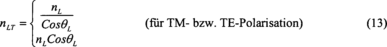
Wenn elektromagnetische Strahlung auf eine Materialoberfläche trifft, können Wellen der Strahlung von dem Material reflektiert werden oder durch das Material durchgelassen werden. Wenn elektromagnetische Strahlung in dem Winkel θ0 auf das erste Ende
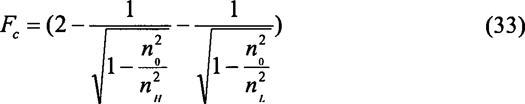
Was das omnidirektionale Reflexionsvermögen betrifft, so verlangt eine notwendige, aber nicht hinreichende Bedingung für den TE-Modus und den TM-Modus der elektromagnetischen Strahlung, dass der maximale Brechungswinkel (θH,MAX) innerhalb der ersten Schicht kleiner ist als der Brewster-Winkel (θB) an der Grenzschicht zwischen der ersten Schicht und der zweiten Schicht. Falls die Bedingung nicht erfüllt ist, wird der TM-Modus der elektromagnetischen Wellen an der zweiten und allen folgenden Grenzen nicht reflektiert und geht somit durch die Struktur hindurch. Daraus folgt: ![]()
![]()
![]()
![]()
Weswegen folgendes notwendig ist: 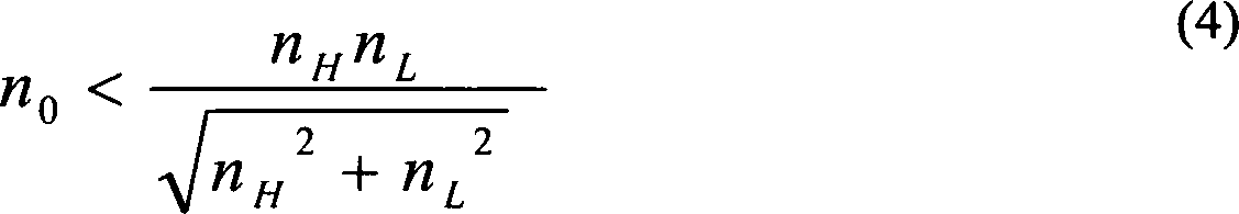
Zusätzlich zu der notwendigen Bedingung, die von Gleichung 4 dargestellt wird, kann, wenn die elektromagnetische Strahlung einer Wellenlänge λ mit einem Winkel θ0 auf eine mehrschichtige Struktur fällt und die einzelnen Zweifachschichten der mehrschichtigen Struktur Dicken dH und dL mit Brechungsindizes nH bzw. nL aufweisen, die charakteristische Translationsmatrix (FT), θ0 ausgedrückt werden als: ![]()
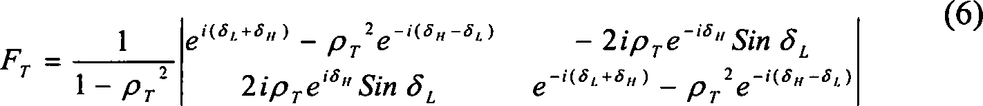
![]()
![]()
![]()
Außerdem gilt ![]()

![]()
Löst man ρT ausdrücklich für TE und TM auf: ![]()
![]()
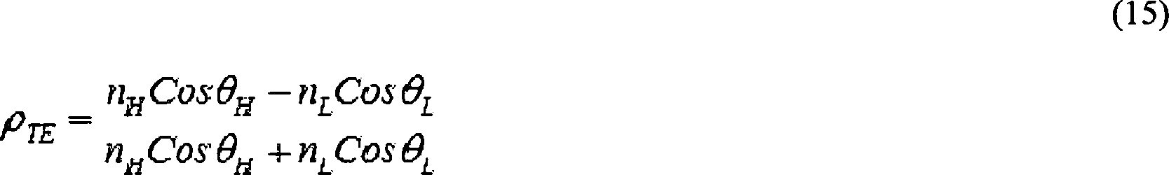
Eine blickwinkelabhängige Bandstruktur kann aus einer Grenzbedingung für den Rand, der sogenannten Bandlücke, der gesamten Reflexionszone erhalten werden. Für die Zwecke der vorliegenden Erfindung wird Bandlücke definiert als Gleichung für die Linie, welche die Totalreflexionszone von der Transmissionszone trennt, für die gegebene Bandstruktur.An angle-dependent band structure can be obtained from a boundary condition for the edge, the so-called bandgap, of the entire reflection zone. For the purposes of the present invention, bandgap is defined as the equation for the line separating the total reflection zone from the transmission zone for the given band structure.
Eine Grenzbedingung, welche die Bandlückenfrequenzen des stark reflektierten Bandes bestimmt, kann angegeben werden durch:
Somit folgt aus +3: ![]()
![]()
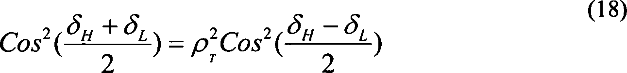
Durch Kombinieren der Gleichungen 15 und 7 wird die folgende Bandlückengleichung erhalten: ![]()
![]()
Wobei:
Das „+”-Zeichen in der oben gezeigten Bandlückengleichung stellt die Bandlücke für die lange Wellenlänge (λlong) dar, und das „–”-Zeichen stellt die Bandlücke für die kurze Wellenlänge (λshort) dar. Stellt man die Gleichungen 20 und 21 um, so erhält man: ![]()
![]()
![]()
![]()
Eine Näherungslösung für die Bandlücke kann durch den folgenden Ausdruck bestimmt werden:
Diese Näherungslösung ist sinnvoll, wenn man ein Viertelwellen-Design (das weiter unten ausführlicher beschrieben wird) betrachtet und optische Dicken der einander abwechselnden Schichten so gewählt werden, dass sie einander gleich sind. Außerdem liefern relativ kleine Unterschiede der optischen Dicken der einander abwechselnden Schichten einen Cosinus, der nahe an eins liegt. Somit liefern die Gleichungen 23 und 24 Bandlücken-Näherungsgleichungen: ![]()
![]()
![]()
![]()
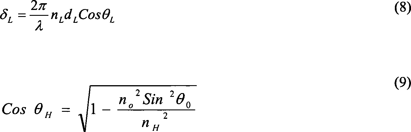
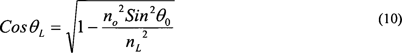
Werte für L+ und ρTM als Funktion des Einfallswinkels können aus den Gleichungen 7, 8, 14, 15, 20 und 21 erhalten werden, wodurch Berechnungen von λlong und λshort im TE- und im TM-Modus als Funktion des Einfallswinkels möglich sind.Values for L + and ρ TM as a function of the angle of incidence can be obtained from
Die Zentralwellenlänge eines omnidirektionalen Reflektors (λc) kann bestimmt werden aus der Beziehung:
Die Zentralwellenlänge kann ein wichtiger Parameter sein, da ihr Wert einen ungefähren Bereich der elektromagnetischen Wellenlänge und/oder des Farbspektrums, die bzw. das reflektiert werden soll, anzeigt. Ein weiterer wichtiger Parameter, der einen Hinweis auf die Breite eines Reflexionsbands geben kann, ist definiert als das Verhältnis eines Bereichs von Wellenlängen innerhalb des omnidirektionalen Reflexionsbands zur Bereichsmitte der Wellenlängen innerhalb des omnidirektionalen Reflexionsbands. Dieses „Verhältnis von Bereich zu Bereichsmitte” (η) wird mathematisch ausgedrückt als: 
![]()
![]()
Man beachte, dass die Streuung der Zentralwellenlänge minimiert werden muss, um das schmale omnidirektionale Band zu erhalten. Somit kann aus Gleichung 27 die Streuung der Zentralwellenlänge ausgedrückt werden als: 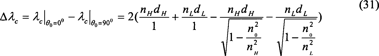
![]()
![]()
Daraus folgend kann ein Mehrschichtstapel mit einer gewünschten niedrigen Verschiebung der Zentralwellenlänge (Δλc) aus einem optisch wenig dichten Material mit einem Brechungsindex von nL und einer oder mehreren Schichten mit einer Dicke von dL und einem optisch dichten Material mit einem Brechungsindex von nH und einer oder mehreren Schichten mit einer Dicke von dH konzipiert werden.As a result, a multilayer stack having a desired low central wavelength shift (Δλ c ) can be made of an optically low density material having a refractive index of n L and one or more layers having a thickness of d L and an optically dense material having a refractive index of n H and one or more layers having a thickness of d H are designed.
Genauer liefert
In
Zweite GenerationSecond generation
Es wird auf
Zum Beispiel liefert
Genauer zeigt
Dritte GenerationThird generation
Es wird auf
Ein Design wie es in
Zum Beispiel ist
Was die Berechnung eines Null- oder Fast-Nullpunkts des elektrischen Feldes betrifft, so zeigt
Bei einer einzelnen dielektrischen Schicht ist θs = θF und die Energie/das elektrische Feld (E) kann ausgedrückt werden als E(z), wenn z = d. Aus den Maxwell-Gleichungen kann das elektrische Feld für eine s-Polarisierung ausgedrückt werden als: ![]()

![]()
Man beachte, dass eine Änderung des elektrischen Feldes entlang der Z-Richtung der dielektrischen Schicht 4 durch eine Berechnung der unbekannten Parameter u(z) und v(z) geschätzt werden kann, wo gezeigt werden kann, dass: ![]()
![]()
Natürlich ist ,i' die Quadratwurzel von –1. Anhand der Grenzbedingungen u|z=0 = 1, v|z=0 = qs und der folgenden Gleichungen: 
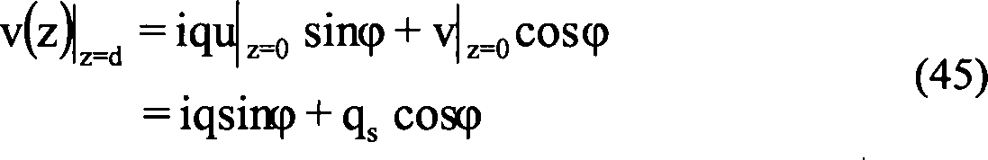
Daher gilt: 
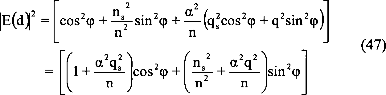

![]()
![]()
Für eine einfache Situation, wo θF = 0 oder ein normaler Einfall ist, φ = k·n·d und α = 0, gilt: 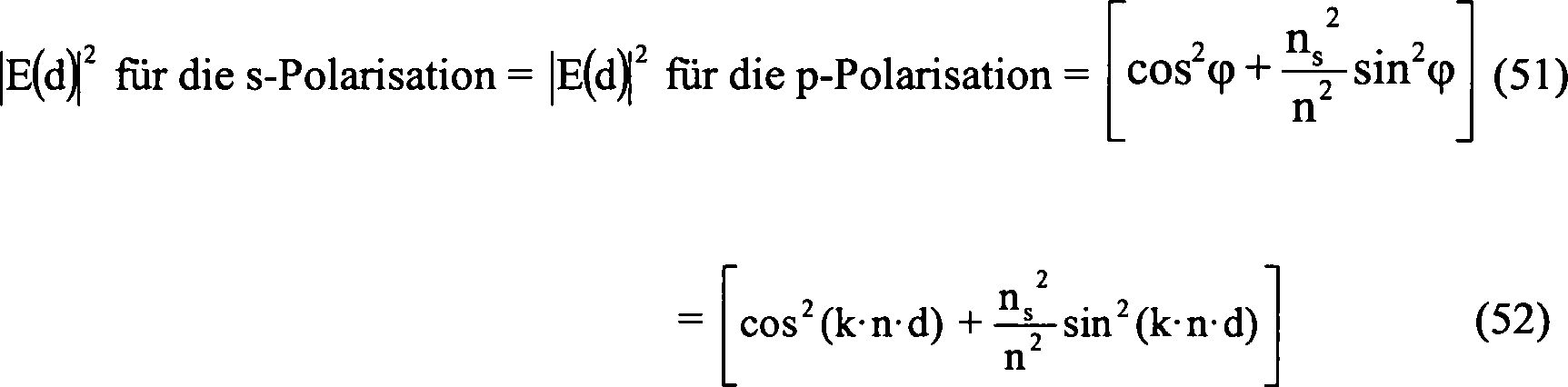
Es wird nun auf
Man beachte, dass ein gewisser Prozentanteil von Licht innerhalb von +/–10 nm der gewünschten 434 nm durch die Cr-ZnS-Grenzschicht hindurchtritt. Man beachte aber auch, dass ein solches schmales Band von reflektiertem Licht, z. B. 434 +/–10 nm für das menschliche Auge immer noch eine scharfe Strukturfarbe liefert.Note that a certain percentage of light passes through the Cr-ZnS interface within +/- 10 nm of the desired 434 nm. But note also that such a narrow band of reflected light, e.g. B. 434 +/- 10 nm for the human eye still provides a sharp structure color.
Das Ergebnis der Cr-Absorberschicht im Mehrschichtstapel in
Im Gegensatz dazu entspricht die durchgezogene Linie in
Was das omnidirektionale Verhalten der in
Um die höhere Winkelvarianz für rote Farbe zu überwinden, offenbart die vorliegende Anmeldung eine einzigartige und neuartige Gestaltung/Struktur, die eine rote Farbe liefert, die winkelunabhängig ist. Zum Beispiel zeigt
Nun wird auf
Man beachte, dass die relativ große Verschiebung in λc für die rote Farbe im Vergleich zur blauen Farbe darauf zurückzuführen ist, dass der dunkelrote Farbraum sehr schmal ist, und auf die Tatsache, dass die Cr-Absorberschicht Wellenlängen absorbiert, die mit einem elektrischen Feld von nicht null assoziiert sind, d. h. dass sie kein Licht absorbiert, wenn das elektrische Feld null oder fast null ist. So zeigt
Genauer zeigt
Auf dieser Basis wurde ein Mehrschichtstapel für eine Machbarkeitsstudie entworfen und hergestellt. Außerdem wurden Rechen-/Simulationsergebnisse und tatsächliche experimentelle Daten für die Machbarkeitsprobe verglichen. Genauer, und wie von der grafischen Darstellung in
Eine Liste simulierter und/oder tatsächlich produzierter Mehrschichtstapelproben ist in der nachstehenden Tabelle 1 angegeben. Wie in der Tabelle dargestellt ist, beinhalten die hierin offenbarten Mehrschichtstrukturen mindestens 5 verschiedene geschichtete Strukturen. Außerdem wurden die Proben aus einem großen Bereich von Materialien simuliert und/oder hergestellt. Es wurden Proben geschaffen, die eine hohe Chrominanz, eine geringe Farbtonverschiebung und einen ausgezeichneten Reflexionsgrad zeigten. Außerdem wiesen die drei- und fünfschichtigen Proben eine Gesamtdicke zwischen 120 und 200 nm auf, die siebenschichtigen Proben wiesen eine Gesamtdicke zwischen 350 und 600 nm auf, die neunschichtigen Proben wiesen eine Gesamtdicke zwischen 440 und 500 nm auf und die elfschichtigen Proben wiesen eine Gesamtdicke zwischen 600 und 660 nm auf. Tabelle 1
Es wird nun auf
Die scharfe Zunahme des Reflexionsgrads, die vom omnidirektionalen Reflektor geleistet wird, ist gekennzeichnet durch einen IR-seitigen Rand jeder Kurve, der von einem schwach reflektierten Abschnitt bei Wellenlängen von über 500 nm bis zu einem stark reflektierten Abschnitt, z. B. > 70% reicht. Ein linearer Abschnitt 200 des IR-seitigen Randes ist in einem Winkel (β) von über 60° in Bezug auf die x-Achse geneigt, weist eine Länge L von ungefähr 50 auf der Reflexionsgradachse und einen Gradienten von 1,2 auf. In manchen Fällen ist der lineare Abschnitt in einem Winkel von über 70° in Bezug auf die x-Achse geneigt, während in anderen Fällen β größer ist als 75°. Ebenso weist das Reflexionsband eine sichtbare FWHM von weniger als 200 nm und in manchen Fällen eine sichtbare FWHM von weniger als 150 nm und in anderen Fällen eine sichtbare FWHM von weniger als 100 nm auf. Außerdem ist die zentrale Wellenlänge λc für das sichtbare Reflexionsband, wie in
Man beachte, dass der Begriff „sichtbare FWHM” die Breite des Reflexionsbands zwischen dem IR-seitigen Rand der Kurve und dem Rand des UV-Spektrumbereichs bezeichnet, jenseits von der die Reflexion, die vom omnidirektionalen Reflektor bereitgestellt wird, für das menschliche Auge nicht sichtbar ist. Auf diese Weise verwenden die hierin offenbarten erfindungsgemäßen Designs und Mehrschichtstapel den nichtsichtbaren UV-Abschnitt des elektromagnetischen Strahlungsspektrums, um eine scharfe oder Strukturfarbe zu schaffen. Anders ausgedrückt nutzen die hierin offenbarten omnidirektionalen Reflektoren den nicht-sichtbaren UV-Abschnitt des elektromagnetischen Strahlungsspektrums, um ein schmales Band des reflektierten sichtbaren Lichtes zu schaffen, trotz der Tatsache, dass die Reflektoren ein viel breiteres Band elektromagnetischer Strahlung reflektieren können, das in die UV-Region hineinreicht.Note that the term "visible FWHM" denotes the width of the reflection band between the IR side edge of the curve and the edge of the UV spectrum region, beyond which the reflection provided by the omnidirectional reflector is not visible to the human eye is. In this way, the inventive designs and multilayer stacks disclosed herein utilize the non-visible UV portion of the electromagnetic radiation spectrum to provide a sharp or textured color. In other words, the omnidirectional reflectors disclosed herein utilize the non-visible UV portion of the electromagnetic radiation spectrum to create a narrow band of reflected visible light, despite the fact that the reflectors can reflect a much wider band of electromagnetic radiation entering the UV Region.
Nun wird auf
Die scharfe Zunahme des Reflexionsgrads, die vom omnidirektionalen Reflektor bereitgestellt wird, ist gekennzeichnet durch einen UV-seitigen Rand jeder Kurve, der von einem schwach reflektierenden Abschnitt bei Wellenlängen von über 550 nm bis zu einem stark reflektierenden Abschnitt, z. B. > 70% reicht. Ein linearer Abschnitt 200 des UV-seitigen Randes ist in einem Winkel (β) von über 60° in Bezug auf die x-Achse geneigt, weist eine Länge L von ungefähr 40 auf der Reflexionsgradachse und einen Gradienten von 1,4 auf. In manchen Fällen ist der lineare Abschnitt in einem Winkel von über 70° in Bezug auf die x-Achse geneigt, während in anderen Fällen β größer ist als 75°. Ebenso weist das Reflexionsband eine sichtbare FWHM von weniger als 200 nm und in manchen Fällen eine sichtbare FWHM von weniger als 150 nm und in anderen Fällen eine sichtbare FWHM von weniger als 100 nm auf. Außerdem ist die Zentralwellenlänge λc für das sichtbare Reflexionsband, wie in
Man beachte, dass der Begriff „sichtbare FWHM” die Breite des Reflexionsbands zwischen dem UV-seitigen Rand der Kurve und dem Rand des IR-Spektrumbereichs bezeichnet, jenseits von der die Reflexion, die vom omnidirektionalen Reflektor bereitgestellt wird, nicht sichtbar ist für das menschliche Auge. Auf diese Weise verwenden die hierin offenbarten erfindungsgemäßen Designs und Mehrschichtstapel den nichtsichtbaren IR-Abschnitt des elektromagnetischen Strahlungsspektrums, um eine scharfe oder Strukturfarbe zu schaffen. Anders ausgedrückt nutzen die hierin offenbarten omnidirektionalen Reflektoren den nicht-sichtbaren IR-Abschnitt des elektromagnetischen Strahlungsspektrums, um ein schmales Band des reflektierten sichtbaren Lichtes zu schaffen, trotz der Tatsache, dass die Reflektoren ein viel breiteres Band elektromagnetischer Strahlung reflektieren können, das in die IR-Region hinein reicht.Note that the term "visible FWHM" denotes the width of the reflection band between the UV-side edge of the curve and the edge of the IR spectrum range, beyond which the reflection provided by the omnidirectional reflector is not visible to the human Eye. In this way, the inventive designs and multilayer stacks disclosed herein utilize the non-visible IR portion of the electromagnetic radiation spectrum to provide a sharp or textured color. In other words, the omnidirectional reflectors disclosed herein utilize the non-visible IR portion of the electromagnetic radiation spectrum to form a narrow band of reflected light visible light, despite the fact that the reflectors can reflect a much broader band of electromagnetic radiation reaching into the IR region.
Es wird nun auf
Wie in
Eine andere Definition oder Charakterisierung von omnidirektionalen Eigenschaften eines Reflektors kann durch die Verschiebung eines Seitenrands für einen gegebenen Satz von Winkelreflexionsbändern bestimmt werden. Zum Beispiel, und wie in
Wie in
Natürlich würde eine Null-Verschiebung, d. h. gar keine Verschiebung (ΔSi = 0 nm; i = IR, UV) einen perfekt omnidirektionalen Reflektor charakterisieren. Jedoch können hierin offenbarte omnidirektionale Reflektoren eine ΔSL von weniger als 50 nm schaffen, was für das menschliche Auge erscheinen kann als ob die Oberfläche des Reflektors die Farbe nicht ändern würde, und somit ist der Reflektor unter einem praktischen Gesichtspunkt omnidirektional. In manchen Fällen können omnidirektionale Reflektoren, die hierin offenbart sind, eine ΔSi von weniger als 40 nm, in anderen Fällen eine ΔSi von weniger als 30 nm und in noch anderen Fällen eine ΔSi von weniger als 20 nm aufweisen, während sie in noch ganz anderen Fällen eine ΔSi von weniger als 15 nm aufweisen. Eine solche Verschiebung in ΔSi kann durch einen Graphen von tatsächlichem Reflexionsgrad gegen Wellenlänge für einen Reflektor und/oder alternativ durch Modellieren des Reflektors, wenn die Materialien und Schichtdicken bekannt sind, bestimmt werden.Of course, a zero displacement, ie no displacement (ΔS i = 0 nm, i = IR, UV) would characterize a perfectly omnidirectional reflector. However, omnidirectional reflectors disclosed herein can provide a ΔS L of less than 50 nm, which may appear to the human eye as if the surface of the reflector did not change color, and thus the reflector is omnidirectional from a practical point of view. In some cases, omnidirectional reflectors disclosed herein may have a ΔS i of less than 40 nm, in other cases a ΔS i of less than 30 nm, and in yet other cases a ΔS i of less than 20 nm, while in FIG still quite different cases have a ΔS i of less than 15 nm. Such a shift in ΔS i can be determined by a graph of actual reflectance versus wavelength for a reflector and / or alternatively by modeling the reflector when the materials and layer thicknesses are known.
Die Verschiebung einer omnidirektionalen Reflexion kann auch durch eine schwache Farbtonverschiebung gemessen werden. Zum Beispiel ist die Farbtonverschiebung der Pigmente, die aus Mehrschichtstapeln gemäß einer Ausführungsform der vorliegenden Erfindung hergestellt sind, 30° oder weniger, wie in
Zusammengefasst ist in
Die erste Schicht
Verfahren zur Herstellung der hierin offenbarten Mehrschichtstapel können beliebige Verfahren oder Prozesse sein, die dem Fachmann bekannt sind, oder (ein) Verfahren, (das) die dem Fachmann noch nicht bekannt (ist) sind. Typische bekannte Verfahren beinhalten Nassverfahren wie Sol-Gel-Verarbeitung, schichtweise Verarbeitung, Schleuderbeschichtung und dergleichen. Andere bekannte, trockene Verfahren beinhalten chemische Dampfabscheidungsverarbeitung und physikalische Dampfabscheidungsverarbeitung wie Sputtern, Elektronenstrahlabscheidung und dergleichen.Methods of making the multilayer stacks disclosed herein may be any methods or processes known to those skilled in the art, or methods that are not known to those skilled in the art. Typical known methods include wet processes such as sol-gel processing, layered processing, spin coating and the like. Other known dry processes include chemical vapor deposition processing and physical vapor deposition processing such as sputtering, electron beam deposition, and the like.
Die hierin offenbarten Mehrschichtstapel können für fast jede Farbanwendung verwendet werden, beispielsweise als Pigmente für Lacke, Dünnfilme, die auf Oberflächen aufgebracht werden, und dergleichen.The multilayer stacks disclosed herein can be used for almost any color application, for example, as pigments for paints, thin films applied to surfaces, and the like.
Wie oben angegeben, werden omnidirektionale Interferenzpigmente geschaffen, die eine schützende/wetterbeständige Beschichtung aufweisen. Zum Beispiel sind in den
Um die Erfindung verständlicher zu machen, aber nicht, um ihren Bereich in irgendeiner Weise einzuschränken, werden nachstehend Beispiele für wetterbeständige omnidirektionale Strukturfarbenpigmente und Prozessprotokolle für die Erzeugung solcher Pigmente erörtert.To make the invention more understandable, but not to limit its scope in any way, examples of weather resistant omnidirectional structural paint pigments and process protocols for the production of such pigments are discussed below.
Protokoll 1 – 7-schichtige Pigmente, die mit Phosphorsäure geätzt und mit einer SiO2-Schicht überzogen werden.Protocol 1 - 7-layer pigments, which are etched with phosphoric acid and coated with a SiO 2 layer.
Zu einer Suspension, die 10 g Pigmente eines 7-schichtigen Designs, die in 110 ml Aceton dispergiert waren, enthielt, wurden 0,13 ml Phosphorsäure (85%) gegeben, und sie wurde 30 Minuten lang bei Raumtemperatur gerührt. Die Suspension wurde dann gefiltert und zweimal mit Aceton gewaschen. Feste Teilchen wurden abfiltriert, und mit Phosphorsäure behandelte 7-schichtige Pigmente wurden erhalten. Die 7-schichtigen Pigmente wiesen eine Struktur auf wie in
Die mit Phosphorsäure behandelten 7-schichtigen Pigmente wurden dann in einem Rundkolben, der mit einem Rückflusskühler ausgestattet war, in 160 ml Ethanol suspendiert. Die Suspension wurde auf 65°C erwärmt, nachdem 35 g Wasser und 3,5 g einer 28%igen wässrigen Ammoniaklösung zugegeben worden waren. Dann wurde eine Lösung aus 10 g Tetraethoxysilan, das mit 13 ml Ethanol verdünnt worden war, in kleinen Mengen unter Rühren zu der erwärmten Suspension hinzugefügt. Die Reaktionsmischung wurde 14 Stunden lang bei 65°C gerührt, dann wurden feste Teilchen aus der Flüssigkeit filtriert, mit Ethanol gewaschen und dann mit Isopropylalkohol (IPA) gewaschen. Siebenschichtige, mit SiO2 beschichtete Pigmente wurden erhalten, nachdem die festen Teilchen 24 Stunden lang bei 100°C getrocknet worden waren. The phosphoric acid-treated 7-layer pigments were then suspended in 160 ml of ethanol in a round bottom flask equipped with a reflux condenser. The suspension was heated to 65 ° C after 35 g of water and 3.5 g of a 28% aqueous ammonia solution were added. Then, a solution of 10 g of tetraethoxysilane diluted with 13 ml of ethanol was added in small portions to the heated suspension with stirring. The reaction mixture was stirred at 65 ° C for 14 hours, then solid particles were filtered from the liquid, washed with ethanol and then washed with isopropyl alcohol (IPA). Seven-layer SiO 2 coated pigments were obtained after the solid particles had been dried at 100 ° C for 24 hours.
Protokoll 1A – 7-schichtige Pigmente, die mit einer SiO2-Schicht überzogen werdenProtocol 1A - 7-layered pigments coated with an SiO 2 layer
Eine Menge von 10 g 7-schichtiger Pigmente wurde in einem Rundkolben, der mit einem Rückflusskühler ausgestattet war, in 160 ml Ethanol suspendiert, ohne zuvor mit Phosphorsäure behandelt zu werden wie in Protokoll 1. Die Suspension wurde auf 65°C erwärmt, nachdem 35 g Wasser und 3,5 g einer 28%igen wässrigen Ammoniaklösung zugegeben worden waren. Dann wurde eine Lösung aus 10 g Tetraethoxysilan, das mit 13 ml Ethanol verdünnt worden war, in kleinen Mengen unter Rühren zu der erwärmten Suspension hinzugefügt. Die Reaktionsmischung wurde 14 Stunden lang bei 65°C gerührt, dann wurden feste Teilchen aus der Flüssigkeit filtriert, mit Ethanol gewaschen und dann mit Isopropylalkohol (IPA) gewaschen. Siebenschichtige, mit SiO2 beschichtete Pigmente wurden erhalten, nachdem die festen Teilchen 24 Stunden lang bei 100°C getrocknet worden waren.An amount of 10 g of 7-layer pigments was suspended in 160 ml of ethanol in a round bottom flask equipped with a reflux condenser without first being treated with phosphoric acid as in
Protokoll 2 – 7-schichtige Pigmente, die unter Verwendung einer wässrigen Lösung mit einer SiO2-Schicht überzogen werdenProtocol 2-7-layered pigments coated with an SiO 2 layer using an aqueous solution
Fünfzehn Gramm 7-schichtiger Pigmente wurden in einen 250 ml fassenden Dreihalskolben gegeben. Dann wurden 100 ml DI-Wasser zugegeben, und die Lösung wurde in einem Ethylenglycol-Bad, das auf 80°C erwärmt wurde, gerührt. Die Lösung wurde durch Zugabe einiger Tropfen einer 1 M NaOH-Lösung auf einen pH von 7,5 eingestellt. Dann wurden 20 ml Na2SiO3 (13 Gew.-% SiO2) mit einer konstanten Strömungsrate von 0,1 ml/min anhand einer Spritzenpumpe zu der Lösung gegeben. Während das Na2SiO3 zugegeben wurde, wurde auch 1 M HCl-Lösung mittels eines automatischen pH-Steuerungssystems zugegeben, um den pH von 7,5 aufrechtzuerhalten. Man ließ die Mischung auf Raumtemperatur abkühlen, filterte sie ab, wusch sie mit IPA und trocknete sie bei 100°C für 24 Stunden. Das beschichtete Material kann bei 200°C 24 h lang weiter getempert werden.Fifteen grams of 7-layer pigments were placed in a 250 ml three-necked flask. Then, 100 ml of DI water was added and the solution was stirred in an ethylene glycol bath heated to 80 ° C. The solution was adjusted to a pH of 7.5 by adding a few drops of a 1 M NaOH solution. Then, 20 ml of Na 2 SiO 3 (13 wt% SiO 2 ) was added to the solution at a constant flow rate of 0.1 ml / min by a syringe pump. While the Na 2 SiO 3 was added, 1 M HCl solution was also added by means of an automatic pH control system to maintain the pH of 7.5. The mixture was allowed to cool to room temperature, filtered off, washed with IPA and dried at 100 ° C for 24 hours. The coated material may be further annealed at 200 ° C for 24 hours.
Protokoll 3 – 7-schichtige Pigmente, die mit einer SiO2-Schicht und einer SiO2-Al2O3-Hybridschicht beschichtet werdenProtocol 3-7-layered pigments coated with an SiO 2 layer and an SiO 2 -Al 2 O 3 hybrid layer
Zwei Gramm Pigmente, die anhand des Protokolls 1 oder 1A mit SiO2 beschichtet worden waren, wurden in 20 ml einer Wasserlösung suspendiert und wiesen einen pH von etwa 10 auf (durch verdünnte NaOH-Lösung eingestellt). Die Suspension wurde unter ständigem Rühren in einem 100 ml fassenden Rundkolben auf 60°C erwärmt. Dann wurden 0,5 ml einer 18 gew.-%igen Na2SiO3-Lösung und 1 ml 0,5 M Al2(SO4)3-Lösung beide gleichzeitig mit einer konstanten Rate in 1 Stunde in die Pigmentsuspension titriert. Der pH der Schlämme wurde nicht gesteuert. Nach der Titrierung wurde die Suspension
Protokoll 4 – 7-schichtige Pigmente, die mit einer SiO2-Schicht und einer ZrO2 + Al2O3-Hybridschicht beschichtet werdenProtocol 4-7-layered pigments coated with an SiO 2 layer and a ZrO 2 + Al 2 O 3 hybrid layer
Drei Gramm Pigmente, die gemäß Protokoll 1 oder 1A mit SiO2 beschichtetet worden waren, wurden in einem 100 ml fassenden Rundkolben mit 20 ml Ethanol beschichtet und bei Raumtemperatur gerührt. Außerdem wurden 0,66 g Aluminium-tri-sek-butoxid und 2,47 ml Zirconiumbutoxid in 15 ml IPA aufgelöst. Die Mischung aus Aluminium-tri-sek-butoxid + Zirconiumbutoxid wurde in 2 Stunden mit einer konstanten Rate in die Pigmentsuspension titriert. Gleichzeitig wurden 0,66 ml DI-Wasser, das in 2 ml Ethanol verdünnt worden war, zudosiert. Nach der Titrierung wurde die Suspension weitere 30 Minuten lang gerührt. Die Mischung wurde filtriert, und die verbliebenen festen Teilchen wurden mit Ethanol gewaschen und dann mit IPA gewaschen. Siebenschichtige Pigmente mit einer SiO2-Schicht und einer ZrO2 + Al2O3-Hybridschicht wurden erhalten, nachdem die verbliebenen Feststoffteilchen 24 Stunden lang bei 100°C getrocknet worden waren oder alternativ dazu 24 Stunden lang bei 200°C weiter getempert worden waren.Three grams of pigments coated with SiO 2 according to
Protokoll 5 – 7-schichtige Pigmente, die mit einer SiO2-Schicht und einer ZrO2 + Al2O3-Hybridschicht beschichtet werden Protocol 5-7-layered pigments coated with an SiO2 layer and a ZrO2 + Al2O3 hybrid layer
Drei Gramm Pigmente, die anhand von Protokoll 1 oder 1A mit SiO2 beschichtet worden waren, wurden in 20 ml DI-Wasser mit pH 8 (durch verdünnte NaOH-Lösung eingestellt) in einem 100 ml fassenden Rundkolben suspendiert und unter konstantem Rühren auf 50°C erwärmt. Dann wurden 0,5 ml einer 5 gew.-%igen NaAlO2-Lösung und 0,5 ml 10 gew.-%ige ZrOCl2-Lösung beide gleichzeitig mit einer konstanten Rate in 30 Minuten in die Pigmentsuspension titriert. Der pH der Schlämme wurde durch Zugabe von verdünnter HCl- oder NaOH-Lösung auf 8 geregelt. Nach der Titrierung wurde die Suspension für 30 min unter Rühren alter gelassen. Die Mischung wurde abfiltriert, mit DI-Wasser gewaschen und dann mit IPA gewaschen. Die beschichteten Pigmente wurden erhalten, nachdem sie 24 Stunden lang bei 100°C getrocknet worden waren oder alternativ dazu 24 Stunden lang bei 200°C getempert worden waren.Three grams of pigments coated with SiO 2 by
Protokoll 6 – 7-schichtige Pigmente, die mit einer SiO2-Schicht, einer CeO2-Schicht und einer ZrO2 + Al2O3-Hybridschicht beschichtet werdenProtocol 6-7-layered pigments which are coated with an SiO 2 layer, a CeO 2 layer and a ZrO 2 + Al 2 O 3 hybrid layer
Pigmente (3,5 g), die anhand von Protokoll 1 oder 1A mit Siliciumoxid (SiO2) beschichtet worden waren, wurden in einem 100 ml fassenden Rundkolben in 26,83 ml Wasser suspendiert und 20 min lang bei 70°C gerührt. Dann wurden 0,33 g Ce(NO3)3·6H2O in 1,18 ml H2O mit einer konstanten Rate von 2 ml/h in die Pigmentsuspension titriert und die Mischung wurden nach dem Titrieren weitere 1,5 Stunden lang am Rühren gehalten. Während der Reaktion wurde der pH der Lösung unter Verwendung einer verdünnten NaOH-Lösung konstant bei 7,0 gehalten. Die Mischung wurde filtriert, und die verbliebenen festen Teilchen wurden dreimal mit Wasser gewaschen und dann weitere drei Mal mit IPA gewaschen. Siebenschichtige Pigmente mit einer SiO2-Schicht und einer Schicht aus CeO2 wurden erhalten, nachdem die verbliebenen festen Teilchen 24 Stunden lang bei 100°C getrocknet worden waren.Pigments (3.5 g) coated with silica (SiO 2 ) by
Dann wurden 3 g der beschichteten Pigmente in einem 100 ml fassenden Rundkolben in 20 ml Ethanol suspendiert und bei Raumtemperatur gerührt. Eine Mischung aus 0,66 g Aluminium-tri-sek-butoxid und 2,47 ml Zirconiumbutoxid, gelöst in 15 ml IPA, wurde mit einer konstanten Rate in 2 Stunden in die Pigmentsuspension titriert. Gleichzeitig wurden 0,66 ml DI-Wasser, verdünnt in 2 ml Ethanol, zudosiert. Nach der Titrierung wurde die Suspension weitere 30 Minuten lang gerührt. Die Mischung wurde filtriert, und die verbliebenen festen Teilchen wurden mit Ethanol gewaschen und dann mit IPA gewaschen. Siebenschichtige Pigmente mit einer SiO2-Schicht, einer Schicht aus CeO2 und einer ZrO2 + Al2O3-Hybridschicht wurden erhalten, nachdem die verbliebenen festen Teilchen 24 Stunden lang bei 100°C getrocknet worden waren.Then, 3 g of the coated pigments were suspended in 20 ml of ethanol in a 100 ml round bottom flask and stirred at room temperature. A mixture of 0.66 g of aluminum tri-sec-butoxide and 2.47 ml of zirconium butoxide dissolved in 15 ml of IPA was titrated into the pigment suspension at a constant rate in 2 hours. At the same time, 0.66 ml DI water, diluted in 2 ml ethanol, was added. After titration, the suspension was stirred for a further 30 minutes. The mixture was filtered and the remaining solid particles were washed with ethanol and then washed with IPA. Seven-layered pigments having an SiO 2 layer, a layer of
Protokoll 7 – 7-schichtige Pigmente, die mit einer CeO2-Schicht und einer ZrO2 + Al2O3-Hybridschicht beschichtet werdenProtocol 7-7-layered pigments coated with a CeO 2 layer and a ZrO 2 + Al 2 O 3 hybrid layer
Drei Gramm Pigmente mit einem 7-Schichten-Design wurden in einem 100 ml fassenden Rundkolben in 20 ml Ethanol suspendiert und bei 75°C gerührt. Eine Lösung aus 0,44 g Ce(NO3)3·6H2O, das in 20 ml IPA aufgelöst worden war, wurde mit einer konstanten Rate in 1 Stunde titriert. Gleichzeitig wurden 0,15 ml Ethylendiamin (EDA), das in 0,9 ml DI-Wasser verdünnt worden war, zudosiert. Danach wurden weitere 0,15 ml EDA, verdünnt in 0,9 ml DI-Wasser, zudosiert. Nach der Titrierung wurde die Suspension weitere 15 Minuten lang gerührt. Die Mischung wurde filtriert und die verbliebenen festen Teilchen wurden mit IPA gewaschen. Siebenschichtige Pigmente mit einer CeO2-Schicht wurden erhalten, nachdem die verbliebenen festen Teilchen 5 Stunden lang bei 100°C getrocknet worden waren.Three grams of pigments with a 7-layer design were suspended in 20 ml of ethanol in a 100 ml round bottomed flask and stirred at 75 ° C. A solution of 0.44 g of Ce (NO 3 ) 3 .6H 2 O dissolved in 20 ml of IPA was titrated at a constant rate in 1 hour. At the same time, 0.15 ml of ethylenediamine (EDA), diluted in 0.9 ml of DI water, was added. Thereafter, an additional 0.15 ml of EDA diluted in 0.9 ml DI water was added. After titration, the suspension was stirred for an additional 15 minutes. The mixture was filtered and the remaining solid particles were washed with IPA. Seven-layered pigments having a CeO 2 layer were obtained after the remaining solid particles were dried at 100 ° C for 5 hours.
Dann wurden die CeO2-beschichteten Pigmente in einem 100 ml fassenden Rundkolben in 20 ml Ethanol suspendiert und bei Raumtemperatur gerührt. Dann wurde eine Mischung aus 0,66 g Aluminium-tri-sek-butoxid und 2,47 ml Zirconiumbutoxid, gelöst in 15 ml IPA, mit einer konstanten Rate in 2 Stunden in die Pigmentsuspension titriert. Gleichzeitig wurden 0,66 ml DI-Wasser, das in 2 ml Ethanol verdünnt worden war, zudosiert. Nach der Titrierung wurde die Suspension weitere 30 Minuten lang gerührt. Die Mischung wurde filtriert, und die verbliebenen festen Teilchen wurden mit Ethanol gewaschen und dann mit IPA gewaschen. Siebenschichtige Pigmente mit einer CeO2-Schicht und einer ZrO2 + Al2O3-Hybridschicht wurden erhalten, nachdem die verbliebenen Feststoffteilchen 24 Stunden lang bei 100°C getrocknet worden waren, oder alternativ dazu 24 Stunden lang bei 200°C getempert worden waren.Then, the CeO 2 -coated pigments were suspended in 20 ml of ethanol in a 100 ml round-bottomed flask and stirred at room temperature. Then, a mixture of 0.66 g of aluminum tri-sec-butoxide and 2.47 ml of zirconium butoxide dissolved in 15 ml of IPA was titrated into the pigment suspension at a constant rate in 2 hours. At the same time, 0.66 ml of DI water diluted in 2 ml of ethanol was added. After titration, the suspension was stirred for a further 30 minutes. The mixture was filtered and the remaining solid particles were washed with ethanol and then washed with IPA. Seven-layered pigments having a CeO 2 layer and a ZrO 2 + Al 2 O 3 hybrid layer were obtained after the remaining solid particles were dried at 100 ° C for 24 hours, or alternatively annealed at 200 ° C for 24 hours ,
Protokoll 8 – 7-schichtige Pigmente, die mit einer ZrO2-Schicht überzogen werden Protocol 8 - 7-layered pigments coated with a ZrO 2 layer
Zwei Gramm Pigmente mit einem 7-Schichten-Design wurden in einem 100 ml fassenden Rundkolben in 30 ml Ethanol suspendiert und bei Raumtemperatur gerührt. Eine Lösung aus 2,75 ml Zirconiumbutoxid (80%ig, in 1 Butanol), die in 10 ml Ethanol verdünnt worden war, wurde mit einer konstanten Rate in 1 Stunde titriert. Gleichzeitig wurden 1 ml DI-Wasser, das in 3 ml Ethanol verdünnt worden war, zudosiert. Nach der Titrierung wurde die Suspension weitere 15 Minuten lang gerührt. Siebenschichtige Pigmente mit einer Schicht aus ZrO2 wurden erhalten, nachdem die verbliebenen festen Teilchen aus der Lösung gefiltert, mit Ethanol gewaschen und 5 Stunden lang bei 100°C getrocknet worden waren oder alternativ dazu 24 Stunden lang bei 200°C getempert worden waren.Two grams of pigments with a 7-layer design were suspended in 30 mL of ethanol in a 100 mL round bottom flask and stirred at room temperature. A solution of 2.75 ml of zirconium butoxide (80% in 1-butanol) diluted in 10 ml of ethanol was titrated at a constant rate in 1 hour. At the same time, 1 ml of DI water, which had been diluted in 3 ml of ethanol, was added. After titration, the suspension was stirred for an additional 15 minutes. Seven-layered pigments with a layer of ZrO 2 were obtained after the remaining solid particles were filtered from the solution, washed with ethanol and dried at 100 ° C for 5 hours, or alternatively annealed at 200 ° C for 24 hours.
Protokoll 9 – 7-schichtige Pigmente, die mit einer SiO2-Schicht und einer Al3O3-Schicht beschichtet werdenProtocol 9-7-layered pigments coated with an SiO 2 layer and an Al 3 O 3 layer
Zwei Gramm Pigmente, die anhand von Protokoll 1 oder 1A mit SiO2 beschichtet worden waren, wurden in 20 ml Wasserlösung mit einem pH von etwa 8 (durch verdünnte NaOH-Lösung eingestellt) in einem 100 ml fassenden Rundkolben suspendiert und unter konstantem Rühren auf 50°C erwärmt. Dann wurden 0,5 ml 5 gew.-%ige NaAlO2-Lösung mit einer konstanten Rate in 30 Minuten in die Pigmentsuspension titriert. Der pH der Schlämme wurde unter Verwendung einer HCl 1M-Lösung auf 8 geregelt. Nach der Titrierung wurde die Suspension 30 Minuten lang unter Rühren alter gelassen. Die Mischung wurde abfiltriert, mit DI-Wasser gewaschen und dann mit IPA gewaschen. Die beschichteten Pigmente wurden erhalten, nachdem sie 24 Stunden lang bei 100°C getrocknet worden waren.Two grams of pigments coated with SiO 2 by
Protokoll 10 – 7-schichtige Pigmente, die mit einer SiO2-Schicht und einer TiO2-Schicht beschichtet werdenProtocol 10 - 7-layered pigments coated with an SiO 2 layer and a TiO 2 layer
Ein 250 ml fassender Dreihals-Rundkolben wurde in ein Ethylenglycol-Ölbad gesetzt, dessen Temperatur auf 80°C eingestellt war. Dann wurden 15 g Blättchen, die gemäß Protokoll 1 oder 1A mit SiO2 beschichtet worden waren, und 100 ml DI-Wasser in den Kolben gegeben und mit 400 UpM gerührt. Die Lösung wurde durch Zugabe einiger weniger Tropfen konzentrierter HCl-Lösung auf einen pH von 2 eingestellt. Eine vorverdünnte 35%ige TiCl4-Lösung wurde dann mit einer konstanten Strömungsrate von 0,1 ml/min über eine Spritzenpumpe titriert. Um den pH konstant zu halten, wurde eine Basenlösung in Form von NaOH-Lösung (8M) durch ein automatisches pH-Steuerungssystem in den Kolben titriert. Während der Abscheidung wurden Blättchenproben in bestimmten Zeitabständen extrahiert, um die Schichtdicke zu bestimmen. Man ließ die Mischung auf Raumtemperatur abkühlen, filterte sie anschließend, wusch sie mit IPA und trocknete sie 24 Stunden lang bei 100°C oder temperte sie alternativ dazu 24 Stunden lang bei 200°C.A 250 ml three necked round bottom flask was placed in an ethylene glycol oil bath set at 80 ° C. Then, 15 g of leaflets coated with SiO 2 according to
Die Wetterbeständigkeit der beschichteten Pigmente wurde auf die folgende Weise geprüft. Sieben zylindrische Pyrexkolben (Fassungsvermögen ca. 120 ml) wurden als Photoreaktorgefäße verwendet. Jeder Kolben enthielt 40 ml einer Lösung aus einem fluoreszierenden roten Farbstoff (Eosin B) (1 × 10⁻⁵ M) und 13,3 mg eines Pigments, das geprüft werden sollte. Die Pigment-Eosin B-Lösung wurden 30 min lang im Dunkeln magnetisch gerührt und dann mit Licht aus einem Sonnenlichtsimulator (Oriel® Sol2ATM Class ABA Solar Simulators) bestrahlt. Für jedes Pigment wurde die gleiche Art von Pigment, das mit einer Aluminiumfolie umwickelt war, als direkte Kontrolle verwendet. Außerdem wurde im Handel erhältliches TiO2 (Degussa P25) als Bezug verwendet, um die photokatalytische Aktivität unter den gleichen Versuchsbedingungen zu vergleichen. UV/Vis-Absorptionsspektren wurden nach 65 Stunden Lichteinwirkung aufgezeichnet, um die photokatalytische Aktivität jeder Probe überprüfen zu können.The weatherability of the coated pigments was tested in the following manner. Seven cylindrical Pyrex flasks (capacity about 120 ml) were used as photoreactive vessels. Each flask contained 40 ml of a solution of a fluorescent red dye (Eosin B) (1 x 10 -5 M) and 13.3 mg of a pigment to be tested. The pigment-eosin B solution were stirred magnetically for 30 min in the dark and then exposed to light from a sunlight simulator (Oriel ® Sol2A TM Class ABA solar simulator) was irradiated. For each pigment, the same type of pigment wrapped with an aluminum foil was used as a direct control. In addition, commercially available TiO 2 (Degussa P25) was used as a reference to compare the photocatalytic activity under the same experimental conditions. UV / Vis absorption spectra were recorded after 65 hours exposure to light to verify the photocatalytic activity of each sample.
Die Ergebnisse der Prüfung wurden als relative photokatalytische Aktivität gegen Pigmenttyp aufgezeichnet wie in
Rasterelektronenmikroskopbilder der 7-schichtigen Pigmente vor und nach der Beschichtung mit einer SiO2-Schicht und einer ZrO2-Al2O3-Schicht (Protokoll 4) sind in den
Ein Überblick über Beschichtungen, das Verfahren, das angewendet wurde, um eine Beschichtung zu bilden, die Beschichtungsdicke, die Gleichmäßigkeit der Beschichtungsdicke und die photokatalytische Aktivität ist in der nachstehenden Tabelle 3 zu finden. Tabelle 3
** im Vergleich zum unbeschichteten 7-schichtigen PigmentAn overview of coatings, the method used to form a coating, the coating thickness, the uniformity of the coating thickness and the photocatalytic activity can be found in Table 3 below. Table 3
** compared to the uncoated 7-layer pigment
Auf dieser Grundlage liefert Tabelle 4 eine Auflistung verschiedener Oxidschichten, Substrate, die beschichtet werden können und Bereiche von Beschichtungsdicken, die in der vorliegenden Lehre enthalten sind. Tabelle 4
Außerdem können die omnidirektionalen Strukturfarbpigmente, die eine schützende Beschichtung aufweisen, einer Organosilan-Oberflächenbehandlung unterzogen werden. Zum Beispiel wurden gemäß einem Beispiel für eine Behandlung gemäß einem Organosilanprotokoll 0,5 g Pigmente, die mit einer oder mehreren der oben erörterten schützenden Beschichtungen überzogen worden waren, in 10 ml einer Lösung aus EtOH/Wasser (4:1) mit einem pH von etwa 5,0 (eingestellt durch verdünnte Essigsäurelösung) in einem 100 ml fassenden Rundkolben suspendiert. Die Schlämme wurde 20 Sekunden lang beschallt und dann 15 Minuten lang bei 500 UpM gerührt. Dann wurden 0,1 bis 0,5 Vol.-% Organosilan als Wirkstoff zu der Schlämme hinzugegeben und die Lösung wurde weitere 2 Stunden bei 500 UpM gerührt. Die Schlämme wurde dann unter Verwendung von DI-Wasser zentrifugiert oder gefiltert, und die verbliebenen Pigmente wurden in 10 ml EtOH/Wasser-Lösung (4:1) erneut dispergiert. Die Pigment-EtOH/Wasser-Schlämme wurde auf 65°C bis zum Rückfluss erwärmt und 30 Minuten lang bei 500 UpM gerührt. Die Schlämme wurde dann unter Verwendung von DI-Wasser und dann IPA zentrifugiert oder gefiltert, um einen Kuchen aus Pigmentteilchen zu produzieren. Schließlich wurde der Kuchen 12 Stunden lang bei 100°C getrocknet.In addition, the omnidirectional structural color pigments having a protective coating may be subjected to an organosilane surface treatment. For example, according to one example of treatment according to an organosilane protocol, 0.5 g of pigments coated with one or more of the protective coatings discussed above were dissolved in 10 ml of a solution of EtOH / water (4: 1) having a pH of about 5.0 (adjusted by dilute acetic acid solution) in a 100 ml round bottom flask. The slurry was sonicated for 20 seconds and then stirred for 15 minutes at 500 rpm. Then, 0.1 to 0.5% by volume of organosilane as an active ingredient was added to the slurry, and the solution was stirred at 500 rpm for further 2 hours. The slurry was then centrifuged or filtered using DI water, and the remaining pigments redispersed in 10 ml EtOH / water (4: 1) solution. The pigmented EtOH / water slurry was heated to 65 ° C to reflux and stirred for 30 minutes at 500 rpm. The slurry was then centrifuged or filtered using DI water and then IPA to produce a cake of pigment particles. Finally, the cake was dried at 100 ° C for 12 hours.
Das Organosilanprotokoll kann jedes dem Fachmann bekannte Organosilan-Kupplungsmittel verwenden, unter anderem zum Beispiel N-(2-Aminoethyl)-3-aminopropyltrimethoxysilan (APTMS), N-[3-(Trimethoxysilyl)propyl]ethylendiamin 3-Methacryloxypropyltrimethoxysilan (MAPTMS), N-[2(vinylbenzylamino)-ethyl]-3-aminoproplyltrimethoxysilan, 3-Glycidoxypropyltrimethoxysilan und dergleichen.The organosilane protocol may utilize any organosilane coupling agent known to those skilled in the art, including, for example, N- (2-aminoethyl) -3-aminopropyltrimethoxysilane (APTMS), N- [3- (trimethoxysilyl) propyl] ethylenediamine, 3-methacryloxypropyltrimethoxysilane (MAPTMS), N - [2 (vinylbenzylamino) ethyl] -3-aminoproplyltrimethoxysilane, 3-glycidoxypropyltrimethoxysilane and the like.
Die obigen Beispiele und Ausführungsformen dienen nur der Erläuterung, und Änderungen, Modifikationen und dergleichen, die dennoch im Bereich der Erfindung liegen, werden für einen Fachmann naheliegend sein. Somit wird der Bereich der Erfindung von den Ansprüchen und ihren Äquivalenten definiert.The above examples and embodiments are for illustration only, and changes, modifications and the like which are nevertheless within the scope of the invention will be apparent to those skilled in the art. Thus, the scope of the invention is defined by the claims and their equivalents.
Claims (7)
Applications Claiming Priority (2)
| Application Number | Priority Date | Filing Date | Title |
|---|---|---|---|
| US14/460,511 | 2014-08-15 | ||
| US14/460,511 US10870740B2 (en) | 2007-08-12 | 2014-08-15 | Non-color shifting multilayer structures and protective coatings thereon |
Publications (1)
| Publication Number | Publication Date |
|---|---|
| DE102015112412A1 true DE102015112412A1 (en) | 2016-02-18 |
Family
ID=55235085
Family Applications (1)
| Application Number | Title | Priority Date | Filing Date |
|---|---|---|---|
| DE102015112412.2A Pending DE102015112412A1 (en) | 2014-08-15 | 2015-07-29 | The color non-altering multi-layer structures and protective coating thereon |
Country Status (3)
| Country | Link |
|---|---|
| JP (2) | JP7040880B2 (en) |
| CN (2) | CN112126248A (en) |
| DE (1) | DE102015112412A1 (en) |
Families Citing this family (6)
| Publication number | Priority date | Publication date | Assignee | Title |
|---|---|---|---|---|
| CN107092046A (en) * | 2017-04-26 | 2017-08-25 | 上海默奥光学薄膜器件有限公司 | A kind of high reflective mirror of wide spectrum |
| CN111880256B (en) * | 2017-09-29 | 2022-03-08 | 耐克创新有限合伙公司 | Structurally colored articles and methods of making and using structurally colored articles |
| US11118062B2 (en) * | 2017-12-06 | 2021-09-14 | Toyota Motor Engineering & Manufacturing North America, Inc. | LiDAR reflecting dark colored pigments and vehicles comprising the same |
| CN110543012B (en) * | 2018-05-29 | 2022-05-17 | 北京以色佳科技有限公司 | Design method of non-energy-consumption artificial intelligence filter with reflecting film and filter |
| KR102841867B1 (en) * | 2020-06-22 | 2025-08-05 | 에카르트 아메리카 코포레이션 | Effect pigments with reflective cores |
| CN115770711A (en) * | 2022-11-30 | 2023-03-10 | 厦门凌太光学有限公司 | Environment-friendly coating process for surface of spectacle lens |
Family Cites Families (30)
| Publication number | Priority date | Publication date | Assignee | Title |
|---|---|---|---|---|
| US5569535A (en) * | 1979-12-28 | 1996-10-29 | Flex Products, Inc. | High chroma multilayer interference platelets |
| US5423912A (en) * | 1993-10-21 | 1995-06-13 | The Mearl Corporation | Weather resistant pearlescent pigments |
| DE4405492A1 (en) * | 1994-02-21 | 1995-08-24 | Basf Ag | Metallic pigments with multiple coatings |
| ATE168713T1 (en) * | 1994-02-21 | 1998-08-15 | Basf Ag | MULTIPLE COATED METALLIC GLOSS PIGMENTS |
| DE19515988A1 (en) * | 1995-05-02 | 1996-11-07 | Basf Ag | Goniochromatic gloss pigments with a coating containing metal sulfide |
| GB9619781D0 (en) * | 1996-09-23 | 1996-11-06 | Secr Defence | Multi layer interference coatings |
| DE19707805A1 (en) * | 1997-02-27 | 1998-09-03 | Merck Patent Gmbh | Multilayer interference pigment with an absorbent middle layer |
| EP0984043A1 (en) * | 1998-08-31 | 2000-03-08 | Sicpa Holding S.A. | Optically variable pigments providing a colour shift between two distinct colours, coating composition comprising the same, method for producing the same and substrate coated with the coating composition |
| US6157489A (en) * | 1998-11-24 | 2000-12-05 | Flex Products, Inc. | Color shifting thin film pigments |
| DE19901612A1 (en) * | 1999-01-19 | 2000-07-20 | Merck Patent Gmbh | Multilayer pearlescent pigments comprise a lamellar substrate with a high refractive index, a layer of a material with a low refractive index and a semitransparent metallic layer |
| JP2002080749A (en) * | 2000-06-29 | 2002-03-19 | Nittetsu Mining Co Ltd | Film-coated powder, coating composition and coated article |
| US6686042B1 (en) * | 2000-09-22 | 2004-02-03 | Flex Products, Inc. | Optically variable pigments and foils with enhanced color shifting properties |
| US6569529B1 (en) * | 2000-10-10 | 2003-05-27 | Flex Product, Inc. | Titanium-containing interference pigments and foils with color shifting properties |
| CN101104748B (en) * | 2001-07-12 | 2012-08-22 | 默克专利股份有限公司 | Multilayer pigments based on glass flakes |
| US6749936B2 (en) * | 2001-12-20 | 2004-06-15 | Flex Products, Inc. | Achromatic multilayer diffractive pigments and foils |
| DE10356357B4 (en) * | 2003-11-28 | 2010-05-06 | Von Ardenne Anlagentechnik Gmbh | Heat-treatable solar and thermal insulation layer system and method for its production |
| DE102004037271A1 (en) | 2004-07-31 | 2006-03-23 | Kronos International, Inc. | Weathering stable titanium dioxide pigment and process for its preparation |
| DE102004041586A1 (en) * | 2004-08-26 | 2006-03-02 | Eckart Gmbh & Co. Kg | Coated pearlescent pigments with SiO 2 and cerium oxide |
| DE102005050094A1 (en) | 2005-10-18 | 2007-04-19 | Identif Gmbh | Colored effect pigment with layer of discrete metal particles, process for its preparation and its use |
| US8951607B2 (en) | 2007-05-03 | 2015-02-10 | Tronox, Llc | Making co-precipitated mixed oxide-treated titanium dioxide pigments |
| US10690823B2 (en) * | 2007-08-12 | 2020-06-23 | Toyota Motor Corporation | Omnidirectional structural color made from metal and dielectric layers |
| US10788608B2 (en) * | 2007-08-12 | 2020-09-29 | Toyota Jidosha Kabushiki Kaisha | Non-color shifting multilayer structures |
| EP2212726A1 (en) * | 2007-10-30 | 2010-08-04 | 3M Innovative Properties Company | Multi-stack optical bandpass film with electro magnetic interference shielding for optical display filters |
| EP2531562B1 (en) * | 2010-02-04 | 2018-01-24 | Basf Se | Pigment compositions with improved sparkling effect |
| JP2013518946A (en) | 2010-02-04 | 2013-05-23 | メルク パテント ゲゼルシャフト ミット ベシュレンクテル ハフツング | Effect pigment |
| US9508475B2 (en) * | 2010-06-30 | 2016-11-29 | Viavi Solutions Inc. | Magnetic multilayer pigment flake and coating composition |
| EP2697295B1 (en) * | 2011-04-14 | 2018-12-19 | Exatec, LLC. | Organic resin laminate |
| BR112014002667A8 (en) * | 2011-08-05 | 2017-06-20 | Construction Research & Technology Gmbh | waterproof coating system to reflect solar radiation and water based coating for decorative and reflective layer formation in the coating system |
| JP6276695B2 (en) * | 2012-10-19 | 2018-02-07 | 日本化薬株式会社 | Heat ray shielding sheet |
| DE112015001639B4 (en) * | 2014-04-01 | 2023-12-14 | Toyota Jidosha Kabushiki Kaisha | NON-COLOR-SHIFTING MULTI-LAYER STRUCTURES |
-
2015
- 2015-07-29 DE DE102015112412.2A patent/DE102015112412A1/en active Pending
- 2015-08-14 CN CN202010927458.7A patent/CN112126248A/en active Pending
- 2015-08-14 CN CN201510498432.4A patent/CN105974501B/en active Active
- 2015-08-17 JP JP2015160731A patent/JP7040880B2/en active Active
-
2020
- 2020-06-18 JP JP2020105083A patent/JP7203790B2/en active Active
Also Published As
| Publication number | Publication date |
|---|---|
| JP2016047917A (en) | 2016-04-07 |
| CN112126248A (en) | 2020-12-25 |
| JP7203790B2 (en) | 2023-01-13 |
| JP7040880B2 (en) | 2022-03-23 |
| JP2020180289A (en) | 2020-11-05 |
| CN105974501A (en) | 2016-09-28 |
| CN105974501B (en) | 2021-01-08 |
Similar Documents
| Publication | Publication Date | Title |
|---|---|---|
| DE112015001639B4 (en) | NON-COLOR-SHIFTING MULTI-LAYER STRUCTURES | |
| DE102014119261B4 (en) | Red omnidirectional structural paint made of metal and dielectric layers | |
| DE102015112412A1 (en) | The color non-altering multi-layer structures and protective coating thereon | |
| US10870740B2 (en) | Non-color shifting multilayer structures and protective coatings thereon | |
| DE112010001362B4 (en) | Process for designing and manufacturing omnidirectional, multilayer photonic structures | |
| US8446666B2 (en) | UV-reflective structural color | |
| DE102016120122C5 (en) | Spectacle lens with coating, method for producing a spectacle lens and computer-implemented or experimental method for designing a spectacle lens | |
| JP6816235B2 (en) | High chroma omnidirectional structure color multilayer structure | |
| DE102016100346A1 (en) | RESISTANT HYBRID PIGMENTS OF AN OMNIDIRECTIONAL STRUCTURAL COLOR FOR EXTERNAL APPLICATIONS | |
| DE2334875C2 (en) | Four-layer anti-reflective coating for an optical glass substrate | |
| DE102015113535B4 (en) | Red omnidirectional structural paint made of metal and dielectric layers | |
| DE2637616A1 (en) | FILTER FOR PHOTODETECTORS | |
| EP2710416A1 (en) | Two-dimensionally periodic, colour-filtering grating | |
| JP6817407B2 (en) | Omnidirectional high saturation red structural color with semiconductor absorber layer | |
| DE102007054701A1 (en) | Color filter and method for its production | |
| EP2460035A1 (en) | Method for producing coatings having anti-reflection properties | |
| EP3317111A1 (en) | Security element with colour-filtering grating | |
| DE2240302C3 (en) | Optical multi-layer anti-reflective coating | |
| DE102016110314A1 (en) | OMNIDIRECTIONAL RED STRUCTURAL COLOR HIGH CHROMA WITH COMBINATION OF SEMICONDUCTOR ABSORBER AND DIELECTRIC ABSORBENT LAYERS | |
| DE112023003781T5 (en) | STRUCTURAL COLOR MULTILAYER STRUCTURES WITH BARRIER LAYERS | |
| DE102016110095A1 (en) | OMNIDIRECTIONAL RED STRUCTURAL COLOR HIGH CHROMA WITH COMBINATION OF METAL ABSORBER AND DIELECTRIC ABSORBENT LAYERS | |
| DE2321159C3 (en) | Seven-layer anti-reflective coating | |
| EP3903127A1 (en) | Interference layer system without a carrier substrate, method for producing same, and use thereof | |
| JP2018087093A (en) | Production method of vanadium dioxide-containing particle, preparation method of fluid dispersion, and fluid dispersion |
Legal Events
| Date | Code | Title | Description |
|---|---|---|---|
| R081 | Change of applicant/patentee |
Owner name: TOYOTA MOTOR ENGINEERING & MANUFACTURING NORTH, US Free format text: FORMER OWNERS: TOYOTA JIDOSHA KABUSHIKI KAISHA, TOYOTA-SHI, AICHI-KEN, JP; TOYOTA MOTOR ENGINEERING & MANUFACTURING NORTH AMERICA INC., ERLANGER, KY., US Owner name: TOYOTA JIDOSHA KABUSHIKI KAISHA, TOYOTA-SHI, JP Free format text: FORMER OWNERS: TOYOTA JIDOSHA KABUSHIKI KAISHA, TOYOTA-SHI, AICHI-KEN, JP; TOYOTA MOTOR ENGINEERING & MANUFACTURING NORTH AMERICA INC., ERLANGER, KY., US |
|
| R082 | Change of representative |
Representative=s name: KUHNEN & WACKER PATENT- UND RECHTSANWALTSBUERO, DE |
|
| R012 | Request for examination validly filed | ||
| R016 | Response to examination communication | ||
| R081 | Change of applicant/patentee |
Owner name: TOYOTA JIDOSHA KABUSHIKI KAISHA, TOYOTA-SHI, JP Free format text: FORMER OWNERS: TOYOTA JIDOSHA KABUSHIKI KAISHA, TOYOTA-SHI, AICHI-KEN, JP; TOYOTA MOTOR ENGINEERING & MANUFACTURING NORTH AMERICA, INC., PLANO, TEX., US |