DE102013107113B4 - Organic light-emitting device and method for producing an organic light-emitting device - Google Patents
Organic light-emitting device and method for producing an organic light-emitting device Download PDFInfo
- Publication number
- DE102013107113B4 DE102013107113B4 DE102013107113.9A DE102013107113A DE102013107113B4 DE 102013107113 B4 DE102013107113 B4 DE 102013107113B4 DE 102013107113 A DE102013107113 A DE 102013107113A DE 102013107113 B4 DE102013107113 B4 DE 102013107113B4
- Authority
- DE
- Germany
- Prior art keywords
- layer
- hole
- transporting layer
- transporting
- multinuclear
- Prior art date
- Legal status (The legal status is an assumption and is not a legal conclusion. Google has not performed a legal analysis and makes no representation as to the accuracy of the status listed.)
- Active
Links
Images


Classifications
-
- H—ELECTRICITY
- H10—SEMICONDUCTOR DEVICES; ELECTRIC SOLID-STATE DEVICES NOT OTHERWISE PROVIDED FOR
- H10K—ORGANIC ELECTRIC SOLID-STATE DEVICES
- H10K85/00—Organic materials used in the body or electrodes of devices covered by this subclass
- H10K85/30—Coordination compounds
- H10K85/311—Phthalocyanine
-
- H—ELECTRICITY
- H10—SEMICONDUCTOR DEVICES; ELECTRIC SOLID-STATE DEVICES NOT OTHERWISE PROVIDED FOR
- H10K—ORGANIC ELECTRIC SOLID-STATE DEVICES
- H10K50/00—Organic light-emitting devices
- H10K50/10—OLEDs or polymer light-emitting diodes [PLED]
- H10K50/14—Carrier transporting layers
- H10K50/15—Hole transporting layers
- H10K50/155—Hole transporting layers comprising dopants
-
- H—ELECTRICITY
- H10—SEMICONDUCTOR DEVICES; ELECTRIC SOLID-STATE DEVICES NOT OTHERWISE PROVIDED FOR
- H10K—ORGANIC ELECTRIC SOLID-STATE DEVICES
- H10K50/00—Organic light-emitting devices
- H10K50/10—OLEDs or polymer light-emitting diodes [PLED]
- H10K50/14—Carrier transporting layers
- H10K50/15—Hole transporting layers
- H10K50/156—Hole transporting layers comprising a multilayered structure
-
- H—ELECTRICITY
- H10—SEMICONDUCTOR DEVICES; ELECTRIC SOLID-STATE DEVICES NOT OTHERWISE PROVIDED FOR
- H10K—ORGANIC ELECTRIC SOLID-STATE DEVICES
- H10K50/00—Organic light-emitting devices
- H10K50/10—OLEDs or polymer light-emitting diodes [PLED]
- H10K50/14—Carrier transporting layers
- H10K50/16—Electron transporting layers
- H10K50/165—Electron transporting layers comprising dopants
-
- H—ELECTRICITY
- H10—SEMICONDUCTOR DEVICES; ELECTRIC SOLID-STATE DEVICES NOT OTHERWISE PROVIDED FOR
- H10K—ORGANIC ELECTRIC SOLID-STATE DEVICES
- H10K50/00—Organic light-emitting devices
- H10K50/10—OLEDs or polymer light-emitting diodes [PLED]
- H10K50/19—Tandem OLEDs
-
- H—ELECTRICITY
- H10—SEMICONDUCTOR DEVICES; ELECTRIC SOLID-STATE DEVICES NOT OTHERWISE PROVIDED FOR
- H10K—ORGANIC ELECTRIC SOLID-STATE DEVICES
- H10K85/00—Organic materials used in the body or electrodes of devices covered by this subclass
- H10K85/30—Coordination compounds
- H10K85/361—Polynuclear complexes, i.e. complexes comprising two or more metal centers
-
- H—ELECTRICITY
- H10—SEMICONDUCTOR DEVICES; ELECTRIC SOLID-STATE DEVICES NOT OTHERWISE PROVIDED FOR
- H10K—ORGANIC ELECTRIC SOLID-STATE DEVICES
- H10K2102/00—Constructional details relating to the organic devices covered by this subclass
- H10K2102/301—Details of OLEDs
- H10K2102/351—Thickness
-
- H—ELECTRICITY
- H10—SEMICONDUCTOR DEVICES; ELECTRIC SOLID-STATE DEVICES NOT OTHERWISE PROVIDED FOR
- H10K—ORGANIC ELECTRIC SOLID-STATE DEVICES
- H10K71/00—Manufacture or treatment specially adapted for the organic devices covered by this subclass
-
- H—ELECTRICITY
- H10—SEMICONDUCTOR DEVICES; ELECTRIC SOLID-STATE DEVICES NOT OTHERWISE PROVIDED FOR
- H10K—ORGANIC ELECTRIC SOLID-STATE DEVICES
- H10K85/00—Organic materials used in the body or electrodes of devices covered by this subclass
- H10K85/30—Coordination compounds
- H10K85/381—Metal complexes comprising a group IIB metal element, e.g. comprising cadmium, mercury or zinc
Landscapes
- Chemical & Material Sciences (AREA)
- Physics & Mathematics (AREA)
- Optics & Photonics (AREA)
- Inorganic Chemistry (AREA)
- Engineering & Computer Science (AREA)
- Materials Engineering (AREA)
- High Energy & Nuclear Physics (AREA)
- Electroluminescent Light Sources (AREA)
Abstract
Organisches Licht emittierendes Bauelement aufweisend ein Substrat (10), eine erste Elektrode (20) auf dem Substrat (10), einen ersten organischen funktionellen Schichtenstapel (30) auf der ersten Elektrode (20), einen Ladungsträgererzeugungs-Schichtenstapel (40) auf dem ersten organischen funktionellen Schichtenstapel (30), einen zweiten organischen funktionellen Schichtenstapel (50) auf dem Ladungsträgererzeugungs-Schichtenstapel (40), und eine zweite Elektrode (60) auf dem zweiten organischen funktionellen Schichtenstapel (50), wobei der Ladungsträgererzeugungs-Schichtenstapel (40) zumindest eine lochtransportierende Schicht (43), eine elektronentransportierende Schicht (41) und eine Zwischenschicht (42) aufweist, und wobei die mindestens eine Zwischenschicht (42) ein multinukleares Phthalocyanin-Derivat aufweist, wobei das multinukleare Phthalocyanin-Derivat durch Annelierung durch Benzolringe von zwei oder mehreren mononuklearen Phthalocyanin-Einheiten erhalten wird.
Description
Es wird ein organisches Licht emittierendes Bauelement und ein Verfahren zur Herstellung eines organischen Licht emittierenden Bauelements angegeben.An organic light-emitting device and a method for producing an organic light-emitting device are specified.
Organische Licht emittierende Bauelemente, wie beispielsweise organische Licht emittierende Dioden (OLED) weisen üblicherweise zumindest eine elektrolumineszierende organische Schicht zwischen zwei Elektroden auf, die als Anode und Kathode ausgebildet sind und mittels derer in die elektrolumineszierende organische Schicht Ladungsträger, also Elektronen und Löcher, injiziert werden können. Hocheffiziente und langlebige OLEDs lassen sich mittels Leitfähigkeitsdotierungen durch die Verwendung eines p-i-n-Übergangs analog zu herkömmlichen anorganischen Licht emittierenden Dioden herstellen, wie beispielsweise in der Druckschrift
Um die Leuchtdichte zu erhöhen und die Lebensdauer zu verlängern, können mehrere OLEDs monolithisch übereinander gestapelt werden, wobei sie elektrisch durch Ladungsträgererzeugungs-Schichtenstapel, so genannte Charge Generation Layers (CGL) verbunden werden. Eine CGL besteht beispielsweise aus einem hoch dotierten p-n-Übergang, der als Tunnelübergang zwischen den gestapelten Emissionsschichten dient. Derartige CGL sind beispielsweise in
Voraussetzung für den Einsatz einer CGL in beispielsweise einer weißen OLED sind ein einfacher Aufbau, das heißt wenige Schichten, die leicht prozessierbar sind, ein geringer Spannungsabfall über der CGL, eine möglichst geringe Änderung des Spannungsabfalls über der CGL während des Betriebs der OLED bei den angestrebten Betriebsbedingungen, sowie eine möglichst hohe Transmission im von der OLED emittierten Spektralbereich, damit Absorptionsverluste des emittierten Lichts vermieden werden.The prerequisites for the use of a CGL in, for example, a white OLED are a simple structure, i.e. few layers that are easy to process, a low voltage drop across the CGL, the smallest possible change in the voltage drop across the CGL during operation of the OLED under the desired operating conditions, and the highest possible transmission in the spectral range emitted by the OLED, so that absorption losses of the emitted light are avoided.
Bekannte CGLs setzen für die p-Dotierung anorganische Materialien, beispielsweise V2O5, MoO3, WO3, oder organische Materialien, beispielsweise F4-TCNQ, Cu(I)pFBz oder Bi(III)pFBz ein. Für die n-Dotierung finden organische Verbindungen wie 1,4,5,8,9,11-Hexaazatriphenylen, Hexacarbonitril (HAT-CN) oder Metalle mit niedriger Austrittsarbeit wie beispielsweise Cs, Li und Mg beziehungsweise Verbindungen daraus (zum Beispiel Cs2CO3, Cs3PO4) Verwendung.Known CGLs use inorganic materials, such as V 2 O 5 , MoO 3 , WO 3 , or organic materials, such as F4-TCNQ, Cu(I)pFBz or Bi(III)pFBz, for p-doping. Organic compounds such as 1,4,5,8,9,11-hexaazatriphenylene, hexacarbonitrile (HAT-CN) or metals with a low work function such as Cs, Li and Mg or compounds thereof (for example Cs 2 CO 3 , Cs 3 PO 4 ) are used for n-doping.
Die Druckschrift
Die Druckschrift
Zumindest eine Aufgabe von bestimmten Ausführungsformen ist es, ein organisches Licht emittierendes Bauelement anzugeben. Eine weitere Aufgabe ist es, ein Verfahren zur Herstellung eines organischen Licht emittierenden Bauelements anzugeben.At least one object of certain embodiments is to specify an organic light-emitting component. A further object is to specify a method for producing an organic light-emitting component.
Diese Aufgaben werden durch Gegenstände gemäß den unabhängigen Patentansprüchen gelöst. Vorteilhafte Ausführungsformen und Weiterbildungen der Gegenstände sind in den abhängigen Ansprüchen gekennzeichnet und gehen weiterhin aus der nachfolgenden Beschreibung und den Zeichnungen hervor.These objects are achieved by objects according to the independent patent claims. Advantageous embodiments and developments of the objects are characterized in the dependent claims and are also apparent from the following description and the drawings.
Es wird ein organisches Licht emittierendes Bauelement angegeben, das ein Substrat, eine erste Elektrode auf dem Substrat, einen ersten organischen funktionellen Schichtenstapel auf der ersten Elektrode, einen Ladungsträgererzeugungs-Schichtenstapel auf dem ersten organischen funktionellen Schichtenstapel, einen zweiten organischen funktionellen Schichtenstapel auf dem Ladungsträgererzeugungs-Schichtenstapel, und eine zweite Elektrode auf dem zweiten organischen funktionellen Schichtenstapel aufweist, wobei der Ladungsträgererzeugungs-Schichtenstapel zumindest eine lochtransportierende Schicht, eine elektronentransportierende Schicht und eine Zwischenschicht aufweist, und wobei die mindestens eine Zwischenschicht ein multinukleares Phthalocyanin-Derivat aufweist.An organic light-emitting component is specified which has a substrate, a first electrode on the substrate, a first organic functional layer stack on the first electrode, a charge carrier generation layer stack on the first organic functional layer stack, a second organic functional layer stack on the charge carrier generation layer stack, and a second electrode on the second organic functional layer stack, wherein the charge carrier generation layer stack has at least one hole-transporting layer, an electron-transporting layer and an intermediate layer, and wherein the at least one intermediate layer has a multinuclear phthalocyanine derivative.
Mit „auf“ bezüglich der Anordnung der Schichten und Schichtstapel ist hier und im folgenden eine prinzipielle Reihenfolge gemeint und ist so zu verstehen, dass eine erste Schicht entweder so auf einer zweiten Schicht angeordnet ist, dass die Schichten eine gemeinsame Grenzfläche haben also in direktem mechanischen und/oder elektrischen Kontakt miteinander stehen, oder dass zwischen der ersten Schicht und der zweiten Schicht noch weitere Schichten angeordnet sind.By "on" with regard to the arrangement of the layers and layer stacks, here and in the following, a basic order is meant and is to be understood that a first layer is either arranged on a second layer in such a way that the layers have a common interface, i.e. are in direct mechanical and/or electrical contact with each other, or that further layers are arranged between the first layer and the second layer.
Die organischen funktionellen Schichtstapel können jeweils Schichten mit organischen Polymeren, organischen Oligomeren, organischen Monomeren, organischen kleinen, nicht-polymeren Molekülen („small molecules“) oder Kombinationen daraus aufweisen. Weiterhin können sie zumindest eine organische Licht emittierende Schicht aufweisen. Als Materialien für die organische Licht emittierende Schicht eignen sich Materialien, die eine Strahlungsemission aufgrund von Fluoreszenz oder Phosphoreszenz aufweisen, beispielsweise Ir- oder Pt-Komplexe, Polyfluoren, Polythiophen oder Polyphenylen oder Derivate, Verbindungen, Mischungen oder Copolymere davon. Die organischen funktionellen Schichtenstapel können weiterhin jeweils eine funktionelle Schicht aufweisen, die als Lochtransportschicht ausgeführt ist, um eine effektive Löcherinjektion in die zumindest eine Licht emittierende Schicht zu ermöglichen. Als Materialien für eine Lochtransportschicht können sich beispielsweise tertiäre Amine, Carbazolderivate, mit Camphersulfonsäure dotiertes Polyanilin oder mit Polystyrolsulfonsäure dotiertes Polyethylendioxythiophen als vorteilhaft erweisen. Die organischen funktionellen Schichtenstapel können weiterhin jeweils eine funktionelle Schicht aufweisen, die als Elektronentransportschicht ausgebildet ist. Darüber hinaus können die organischen funktionellen Schichtenstapel auch Elektronen- und/oder Löcherblockierschichten aufweisen.The organic functional layer stacks can each have layers with organic polymers, organic oligomers, organic monomers, organic small, non-polymeric molecules (“small molecules”) or combinations thereof. They can also have at least one organic light-emitting layer. Suitable materials for the organic light-emitting layer are materials that emit radiation due to fluorescence or phosphorescence, for example Ir or Pt complexes, polyfluorene, polythiophene or polyphenylene or derivatives, compounds, mixtures or copolymers thereof. The organic functional layer stacks can also each have a functional layer that is designed as a hole transport layer in order to enable effective hole injection into the at least one light-emitting layer. Tertiary amines, carbazole derivatives, polyaniline doped with camphorsulfonic acid or polyethylenedioxythiophene doped with polystyrenesulfonic acid can, for example, prove to be advantageous as materials for a hole transport layer. The organic functional layer stacks can furthermore each have a functional layer that is designed as an electron transport layer. In addition, the organic functional layer stacks can also have electron and/or hole blocking layers.
Im Hinblick auf den prinzipiellen Aufbau eines organischen Licht emittierenden Bauelements, dabei beispielsweise im Hinblick auf den Aufbau, die Schichtzusammensetzung und die Materialien des organischen funktionellen Schichtenstapels, wird auf die Druckschrift
Das Substrat kann beispielsweise eines oder mehrere Materialien in Form einer Schicht, einer Platte, einer Folie oder einem Laminat aufweisen, die ausgewählt sind aus Glas, Quarz, Kunststoff, Metall und Siliziumwafer. Besonders bevorzugt weist das Substrat Glas, beispielsweise in Form einer Glasschicht, Glasfolie oder Glasplatte, auf oder es besteht daraus.The substrate can, for example, comprise one or more materials in the form of a layer, a plate, a film or a laminate, which are selected from glass, quartz, plastic, metal and silicon wafer. The substrate particularly preferably comprises glass, for example in the form of a glass layer, glass film or glass plate, or consists of glass.
Die zwei Elektroden, zwischen denen die organischen funktionellen Schichtenstapel angeordnet sind, können beispielsweise beide transluzent ausgebildet sein, sodass das in der zumindest einen Licht emittierenden Schicht zwischen den beiden Elektroden erzeugte Licht in beide Richtungen, also in Richtung des Substrats als auch in die vom Substrat abgewandte Richtung, abgestrahlt werden können. Weiterhin können beispielsweise alle Schichten des organischen Licht emittierenden Bauelements transluzent ausgebildet sein, sodass das organische Licht emittierende Bauelement eine transluzente und insbesondere eine transparente OLED bildet. Darüber hinaus kann es auch möglich sein, dass eine der beiden Elektroden, zwischen denen die organischen funktionellen Schichtenstapel angeordnet sind, nichttransluzent und vorzugsweise reflektierend ausgebildet ist, sodass das in der zumindest einen Licht emittierenden Schicht zwischen den beiden Elektroden erzeugte Licht nur in eine Richtung durch die transluzente Elektrode abgestrahlt werden kann. Ist die auf dem Substrat angeordnete Elektrode transluzent und ist auch das Substrat transluzent ausgebildet, so spricht man auch von einem so genannten „bottom emitter“, während man im Fall, dass die dem Substrat abgewandt angeordnete Elektrode transluzent ausgebildet ist, von einem so genannten „top emitter“ spricht.The two electrodes between which the organic functional layer stacks are arranged can, for example, both be translucent, so that the light generated in the at least one light-emitting layer between the two electrodes can be emitted in both directions, i.e. in the direction of the substrate and in the direction facing away from the substrate. Furthermore, for example, all layers of the organic light-emitting component can be translucent, so that the organic light-emitting component forms a translucent and in particular a transparent OLED. In addition, it can also be possible for one of the two electrodes between which the organic functional layer stacks are arranged to be non-translucent and preferably reflective, so that the light generated in the at least one light-emitting layer between the two electrodes can only be emitted in one direction through the translucent electrode. If the electrode arranged on the substrate is translucent and the substrate is also translucent, it is referred to as a so-called “bottom emitter”, whereas if the electrode arranged facing away from the substrate is translucent, it is referred to as a so-called “top emitter”.
Die erste und die zweite Elektrode können unabhängig voneinander ein Material aufweisen, das aus einer Gruppe ausgewählt ist, die Metalle, elektrisch leitfähige Polymere, Übergangsmetalloxide und leitfähige transparente Oxide (transparent conductive oxide, TCO) umfasst. Die Elektroden können auch Schichtenstapel mehrerer Schichten desselben oder unterschiedlicher Metalle oder desselben oder unterschiedlicher TCOs sein.The first and second electrodes may independently comprise a material selected from a group comprising metals, electrically conductive polymers, transition metal oxides, and transparent conductive oxides (TCOs). The electrodes may also be layer stacks of multiple layers of the same or different metals or the same or different TCOs.
Geeignete Metalle sind beispielsweise Ag, Pt, Au, Mg, Al, Ba, In, Ca, Sm oder Li, sowie Verbindungen, Kombinationen oder Legierungen daraus.Suitable metals include Ag, Pt, Au, Mg, Al, Ba, In, Ca, Sm or Li, as well as compounds, combinations or alloys thereof.
Transparente leitende Oxide (transparent conductive oxides, kurz „TCO“) sind transparente, leitende Materialien, in der Regel Metalloxide, wie beispielsweise Zinkoxid, Zinnoxid, Cadmiumoxid, Titanoxid, Indiumoxid oder Indiumzinnoxid (ITO). Neben binären Metallsauerstoffverbindungen, wie beispielsweise ZnO, SnO2 oder In2O3 gehören auch ternäre Metallsauerstoffverbindungen, wie beispielsweise Zn2SnO4, CdSnO3, ZnSnO3, MgIn2O4, GaInO3, Zn2In2O5 oder In4Sn3O12 oder Mischungen unterschiedlicher transparenter leitender Oxide zu der Gruppe der TCOs. Weiterhin entsprechen die TCOs nicht zwingend einer stöchiometrischen Zusammensetzung und können auch p- oder n-dotiert sein.Transparent conductive oxides (TCO) are transparent, conductive materials, usually metal oxides, such as zinc oxide, tin oxide, cadmium oxide, titanium oxide, indium oxide or indium tin oxide (ITO). In addition to binary metal-oxygen compounds, such as ZnO, SnO 2 or In 2 O 3, there are also ternary metal-oxygen compounds, such as Zn 2 SnO 4 , CdSnO3, ZnSnO 3 , MgIn 2 O 4 , GaInO 3 , Zn 2 In 2 O 5 or In 4 Sn 3 O 12 or mixtures of different transparent oxides. less conductive oxides belong to the group of TCOs. Furthermore, the TCOs do not necessarily correspond to a stoichiometric composition and can also be p- or n-doped.
Die organischen funktionellen Schichtenstapel des hier beschriebenen organischen Licht emittierenden Bauelements weisen weiterhin unmittelbar angrenzend einen Ladungsträgererzeugungs-Schichtenstapel auf. Mit einem „Ladungsträgererzeugungs-Schichtenstapel“ wird hier und im Folgenden eine Schichtenfolge beschrieben, die als Tunnelübergang ausgebildet ist und die im Allgemeinen durch einen p-n-Übergang gebildet wird. Der Ladungsträgererzeugungs-Schichtenstapel, der auch als so genannte „charge generation layer“ (CGL) bezeichnet werden kann, ist insbesondere als Tunnelübergang ausgebildet, der zu einer effektiven Ladungstrennung und damit zur „Erzeugung“ von Ladungsträgern für die angrenzenden Schichten eingesetzt werden kann.The organic functional layer stacks of the organic light-emitting component described here also have a charge carrier generation layer stack immediately adjacent to them. A "charge carrier generation layer stack" is used here and below to describe a layer sequence that is designed as a tunnel junction and is generally formed by a p-n junction. The charge carrier generation layer stack, which can also be referred to as a so-called "charge generation layer" (CGL), is designed in particular as a tunnel junction that can be used for effective charge separation and thus for "generating" charge carriers for the adjacent layers.
Beispielsweise kann der Ladungsträgererzeugungs-Schichtenstapel direkt an die organischen funktionellen Schichtenstapel angrenzen.For example, the charge carrier generation layer stack can be directly adjacent to the organic functional layer stacks.
Die lochtransportierende Schicht des Ladungsträgererzeugungs-Schichtenstapels kann auch als p-leitende Schicht, die elektronentransportierende Schicht als n-leitende Schicht bezeichnet werden. Die Zwischenschicht des Ladungsträgererzeugungs-Schichtenstapels kann auch als Diffusionsbarriereschicht gemäß ihrer Funktion bezeichnet werden. Sie kann ein multinukleares Phthalocyanin-Derivat aufweisen oder daraus bestehen.The hole-transporting layer of the charge carrier generation layer stack can also be referred to as a p-conducting layer, the electron-transporting layer as an n-conducting layer. The intermediate layer of the charge carrier generation layer stack can also be referred to as a diffusion barrier layer according to its function. It can comprise or consist of a multinuclear phthalocyanine derivative.
Multinukleare Phthalocyanin-Derivate werden durch Anelierung, das heißt Verknüpfung durch Benzolringe von zwei oder mehreren mononuklearen Phthalocyanin-Derivaten bzw. Phthalocyanin-Einheiten, erhalten. Durch die Anelierung können die photophysikalischen Eigenschaften von Phthalocyanin-Molekülen gezielt verändert werden, wobei eine hohe chemische Stabilität erhalten bleibt. Dadurch kann Einfluss auf das emittierte Spektrum des organischen Licht emittierenden Bauelements genommen werden. Insbesondere können, im Vergleich zu mononuklearen Phthalocyaninen, die langwelligen Absorptionen durch Vergrößerung des Chromophorensystems, also eine Delokalisierung über das gesamte Molekülgerüst, vom gelb-roten in den infraroten Spektralbereich verschoben werden. Die hochenergetischen Übergänge, die im nahen UV-Bereich liegen, werden durch die Anelierung dagegen nicht beeinflusst und führen somit zu keinen Absorptionsverlusten im sichtbaren Bereich. Die resultierenden vergrößerten Moleküle sind wie das mononukleare Phthalocyanin sehr stabil und aggregieren gut, das heißt sie lagern sich bei Aufdampfung plättchenweise auf dem Substrat an.Multinuclear phthalocyanine derivatives are obtained by annealing, i.e. linking two or more mononuclear phthalocyanine derivatives or phthalocyanine units through benzene rings. The annealing can be used to specifically change the photophysical properties of phthalocyanine molecules, while maintaining a high level of chemical stability. This can influence the emitted spectrum of the organic light-emitting component. In particular, compared to mononuclear phthalocyanines, the long-wave absorptions can be shifted from the yellow-red to the infrared spectral range by enlarging the chromophore system, i.e. delocalization over the entire molecular framework. The high-energy transitions in the near UV range, on the other hand, are not affected by the annealing and therefore do not lead to any absorption losses in the visible range. The resulting enlarged molecules, like mononuclear phthalocyanine, are very stable and aggregate well, i.e. they deposit platelet-wise on the substrate when vapor-deposited.
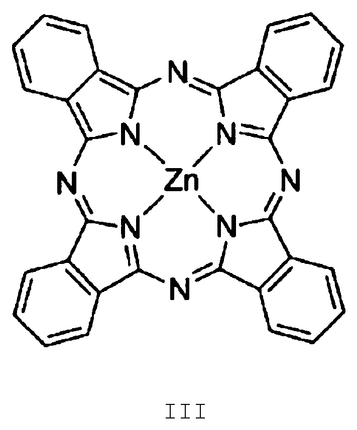
Bei mononuklearen Phthalocyaninen ist die Ausdehnung des π-Elektronensystems auf das monomere Phthalocyanin-Gerüst beschränkt. Beispielhafte mononukleare Phthalocyanine sind in den Strukturformen I bis III gezeigt, wobei die Formeln I und II in oxidierter Form vorliegen. Strukturformel I zeigt das Phthalocyanin VOPc, Strukturformel II zeigt das Phthalocyanin TiOPc und Strukturformel III zeigt das Phthalocyanin ZnPc. 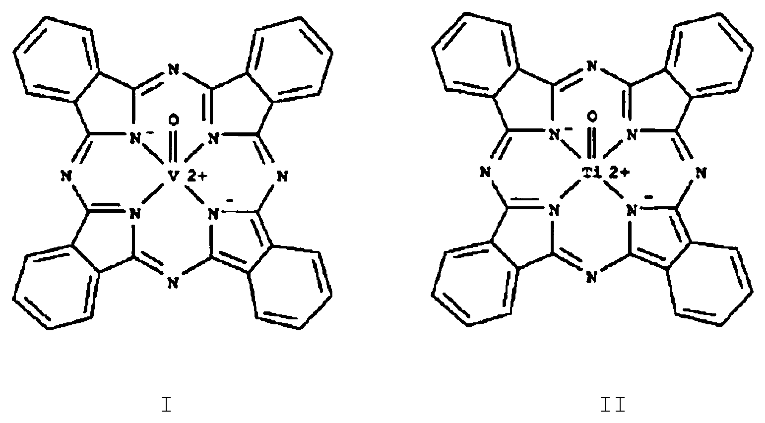
Durch die Anelierung der Monomereinheiten werden diese chemisch gekoppelt. Es resultiert eine Ausdehnung des π-Elektronensystems und eine durch Verschiebung des Absorptionspeaks vom gelb-roten in den infraroten Spektralbereich gekennzeichnete Stabilisierung der niederenergetischen elektronischen Zustände.The monomer units are chemically coupled by annealing. This results in an expansion of the π-electron system and a stabilization of the low-energy electronic states, characterized by a shift of the absorption peak from the yellow-red to the infrared spectral range.
Bei Verwendung eines anelierten multinuklearen Phthalocyanin-Derivats in der Zwischenschicht des Ladungsträgererzeugungs-Schichtenstapels ergibt sich somit eine verringerte Absorption im von dem organischen funktionellen Schichtenstapel emittierten Spektralbereich, wodurch eine erhöhte Effizienz des Bauelements resultiert. Diesen Vorteil erhält man bei gleichzeitig gegenüber mononuklearen Phthalocyaninen unveränderter Stabilität des Ladungsträgererzeugungs-Schichtenstapels.Using a fused multinuclear phthalocyanine derivative in the intermediate layer of the charge carrier generation layer stack results in reduced absorption in the spectral range emitted by the organic functional layer stack, resulting in increased efficiency of the component. This advantage is achieved while at the same time the stability of the charge carrier generation layer stack remains unchanged compared to mononuclear phthalocyanines.
Das multinukleare Phthalocyanin-Derivat kann ein Metall oder eine Metallverbindung enthalten. Somit kann jede Phthalocyanin-Einheit des multinuklearen Phthalocyanin-Derivats zu jeweils einem Metall oder einer Metallverbindung eine oder mehrere chemische Bindungen aufweisen und/oder jede Phthalocyanin-Einheit des multinuklearen Phthalocyanin-Derivats kann jeweils an ein Metall oder eine Metallverbindung koordiniert sein. Als Metall oder Metallverbindung können Materialien ausgewählt werden, die aus einer Gruppe ausgewählt sind, die Cu, Zn, Co, Al, Ni, Fe, SnO, Mn, Mg, VO und TiO enthält. Das bedeutet, dass das Phthalocyanin-Derivat in oxidierter Form vorliegen kann, wenn ein Metalloxid eingesetzt wird. Die Oxidation kann das Phthalocyanin-Derivat gegenüber der nicht oxidierten Form stabilisieren. Gemäß einer weiteren Ausführungsform kann das multinukleare Phthalocyanin-Derivat auch metallfrei sein.The multinuclear phthalocyanine derivative can contain a metal or a metal compound. Thus, each phthalocyanine unit of the multinuclear phthalocyanine derivative can have one or more chemical bonds to a metal or a metal compound and/or each phthalocyanine unit of the multinuclear phthalocyanine derivative can be coordinated to a metal or a metal compound. Materials selected from a group containing Cu, Zn, Co, Al, Ni, Fe, SnO, Mn, Mg, VO and TiO can be selected as the metal or metal compound. This means that the phthalocyanine derivative can be in oxidized form if a metal oxide is used. The oxidation can stabilize the phthalocyanine derivative compared to the non-oxidized form. According to a further embodiment, the multinuclear phthalocyanine derivative can also be metal-free.
Das multinukleare Phthalocyanin-Derivat kann ein dinukleares Phthalocyanin-Derivat sein. Ein Beispiel für ein metallfreies dinukleares Phthalocyanin-Derivat ist in Strukturformel IV gezeigt: 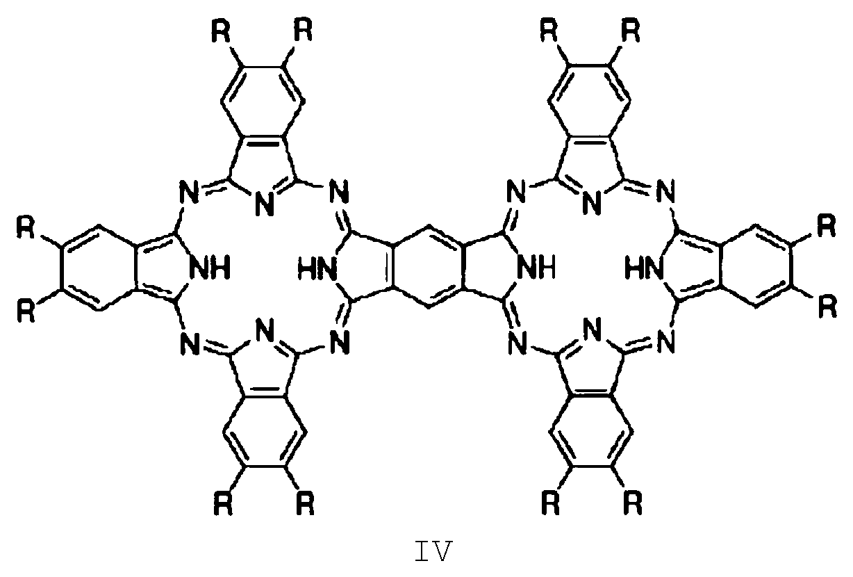
Es handelt sich dabei um H2Pc-H2Pc. Die Reste R in der Strukturformel IV können unabhängig voneinander ausgewählt werden aus: verzweigten oder unverzweigten Alkylresten, wie beispielsweise Methyl-, Ethyl-, t-Butyl- oder iso-Propyl-Resten, und aromatischen Resten, wie beispielsweise Phenylresten.This is H 2 Pc-H 2 Pc. The R radicals in the structural formula IV can be selected independently from: branched or unbranched alkyl radicals, such as methyl, ethyl, t-butyl or isopropyl radicals, and aromatic radicals, such as phenyl radicals.
Ein Beispiel für ein metallhaltiges dinukleares Phthalocyanin-Derivat ist in der Strukturformel V gezeigt: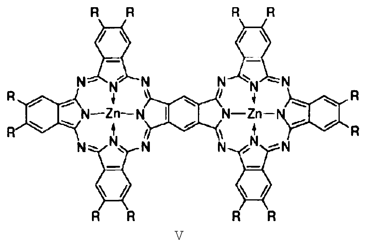
Hierbei handelt es sich um ZnPc-ZnPc. Die Reste R können wie für Strukturformel IV angegeben ausgewählt werden.This is ZnPc-ZnPc. The R residues can be selected as indicated for structural formula IV.
Das multinukleare Phthalocyanin-Derviat kann ein tri- oder tetranukleares Phthalocyanin-Derivat sein. Das tri- oder tetranukleare Phthalocyanin-Derivat kann lineare oder rechtwinklig aneinander anelierte Phthalocyanin-Derviate umfassen. Ein Beispiel für ein lineares trinukleares Phthalocyanin-Derivat ist in Strukturformel VI am Beispiel eines Zink enthaltenden Phthalocyanin-Derivats gezeigt: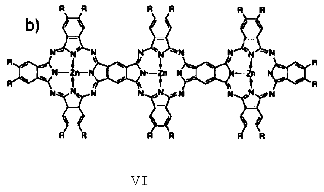
Die Strukturformel VII zeigt ein trinukleares, rechtwinklig aneliertes, Zink enthaltendes Phthalocyanin:
Die Reste R in den Strukturformeln VI und VII können wie für die Strukturformel IV angegeben ausgewählt werden. Multinukleare Phthalocyanin-Derivate mit fünf oder mehr Phthalocyanin-Einheiten sind ebenso denkbar.The R radicals in structural formulae VI and VII can be selected as indicated for structural formula IV. Multinuclear phthalocyanine derivatives with five or more phthalocyanine units are also conceivable.
Die Zwischenschicht, die das multinukleare Phthalocyanin-Derviat aufweist oder daraus besteht kann eine Dicke aufweisen, die aus einem Bereich ausgewählt ist, der 1 bis 50 nm, insbesondere 2 nm bis 10 nm umfasst. Die Dicke der Zwischenschicht kann insbesondere etwa 4 nm betragen. Zwischenschichten, die multinukleare Phthalocyanin-Derivate aufweisen oder daraus bestehen, können besonders dick ausgeformt werden, da durch den Einsatz des multinuklearen Phthalocyanin-Derivats wenig Absorptionsverluste auftreten. Dies gilt sowohl für metallfreie als auch für metallhaltige anelierte multinukleare Phthalocyanin-Derivate. Je dicker die Zwischenschicht ausgeführt ist, desto besser kann die Trennung von n- und p-Seite, also die Trennung der lochtransportierenden Schicht und der elektronentransportierenden Schicht des Ladungsträgererzeugungs-Schichtenstapels realisiert werden.The intermediate layer which has or consists of the multinuclear phthalocyanine derivative can have a thickness which is selected from a range which includes 1 to 50 nm, in particular 2 nm to 10 nm. The thickness of the intermediate layer can in particular be approximately 4 nm. Intermediate layers which have or consist of multinuclear phthalocyanine derivatives can be made particularly thick, since the use of the multinuclear phthalocyanine derivative results in little absorption loss. This applies to both metal-free and metal-containing fused multinuclear phthalocyanine derivatives. The thicker the intermediate layer, the better the separation of the n- and p-sides, i.e. the separation of the hole-transporting layer and the electron-transporting layer of the charge carrier generation layer stack, can be achieved.
Die Transmission der multinuklearen Phthalocyanin-Derivate wird im sichtbaren Wellenlängenbereich, also zwischen etwa 400 und 700 nm, vorteilhaft erhöht im Vergleich zu den bisher eingesetzen Materialien CuPc, H2Pc, ZnPc, CoPc, SnOPc, VOPc, TiOPc oder NET-39. Damit wird die Restabsorption in dem organischen Licht emittierenden Bauelement speziell im gelb-roten Bereich reduziert, der beispielsweise bei weißen OLEDs den Hauptanteil der emittierten Strahlung ausmacht. Die OLED-Effizienz kann folglich erhöht werden. Insbesondere in organischen Licht emittierenden Bauelementen mit interner Auskopplung ist aufgrund der hierbei auftretenden Vielfachreflexionen eine Reduktion der Restabsorption in den organischen Schichten entscheidend, um hohe Effizienzen zu erreichen.The transmission of the multinuclear phthalocyanine derivatives is advantageously increased in the visible wavelength range, i.e. between about 400 and 700 nm, compared to the materials CuPc, H 2 Pc, ZnPc, CoPc, SnOPc, VOPc, TiOPc or NET-39 used to date. This reduces the residual absorption in the organic light-emitting component, especially in the yellow-red range, which accounts for the majority of the emitted radiation in white OLEDs, for example. The OLED efficiency can therefore be increased. In particular in organic light-emitting components with internal coupling, a reduction in the residual absorption in the organic layers is crucial in order to achieve high efficiencies due to the multiple reflections that occur here.
Da die monomeren Phthalocyanin-Derviate bzw. -Einheiten durch starre Benzolringe miteinander verbunden sind, weisen die multinuklearen Phthalocyanin-Derviate in der Zwischenschicht eine hervorragende Morphologie auf und sind in ihren Aggregationseigenschaften in dünnen Filmen kleineren Molekülen, beispielsweise monomoren Phthalocyanin-Derivaten, überlegen. Bei Verwendung anelierter, multinuklearer Phthalocyanin-Derivate können somit bei gleichbleibender Stabilität dünnere Zwischenschichten realisiert werden als mit bekannten Monomereinheiten, was zu einer Verringerung von Absorptions- und Spannungsverlusten führt.Since the monomeric phthalocyanine derivatives or units are connected to one another by rigid benzene rings, the multinuclear phthalocyanine derivatives in the intermediate layer have an excellent morphology and are superior in their aggregation properties in thin films to smaller molecules, such as monomeric phthalocyanine derivatives. When using fused, multinuclear phthalocyanine derivatives, thinner intermediate layers can be realized with the same stability than with known monomer units, which leads to a reduction in absorption and voltage losses.
Die lochtransportierende Schicht kann auf der Zwischenschicht angeordnet sein, welche wiederum auf der elektronentransportierenden Schicht angeordnet ist.The hole-transporting layer can be arranged on the intermediate layer, which in turn is arranged on the electron-transporting layer.
Die lochtransportierende Schicht des Ladungsträgererzeugungs-Schichtenstapels kann weiterhin eine erste lochtransportierende Schicht und eine zweite lochtransportierende Schicht umfassen, und die erste lochtransportierende Schicht kann auf der elektronentransportierenden Schicht und die zweite lochtransportierende Schicht auf der ersten lochtransportierenden Schicht angeordnet sein. Die Zwischenschicht kann zwischen der elektronentransportierenden Schicht und der ersten lochtransportierenden Schicht und/oder zwischen der ersten lochtransportierenden Schicht und der zweiten lochtransportierenden Schicht angeordnet sein. Somit können entweder ein oder zwei Zwischenschichten in dem Ladungsträgererzeugungs-Schichtenstapel vorhanden sein, und, im Falle dass nur eine Zwischenschicht vorhanden ist, kann diese an zwei verschiedenen Positionen vorhanden sein. The hole-transporting layer of the charge carrier generation layer stack may further comprise a first hole-transporting layer and a second hole-transporting layer, and the first hole-transporting layer may be arranged on the electron-transporting layer and the second hole-transporting layer on the first hole-transporting layer. The intermediate layer may be arranged between the electron-transporting layer and the first hole-transporting layer and/or between the first hole-transporting layer and the second hole-transporting layer. Thus, either one or two intermediate layers may be present in the charge carrier generation layer stack, and, in case only one intermediate layer is present, it may be present at two different positions.
Die lochtransportierende Schicht, die erste und die zweite lochtransportierende Schicht können unabhängig voneinander undotiert oder p-dotiert sein. Die p-Dotierung kann beispielsweise einen Anteil in der Schicht von weniger als 10 Volumen%, insbesondere von weniger als 1 Volumen% aufweisen. Die elektronentransportierende Schicht kann undotiert oder n-dotiert sein. Beispielsweise kann die elektronentransportierende Schicht n-dotiert sein und die erste und zweite lochtransportierende Schicht undotiert sein. Weiterhin kann die elektronenetransportierende Schicht beispielsweise n-dotiert sein und die zweite lochtransportierende Schicht p-dotiert sein.The hole-transporting layer, the first and the second hole-transporting layer can be undoped or p-doped independently of one another. The p-doping can, for example, have a proportion in the layer of less than 10% by volume, in particular less than 1% by volume. The electron-transporting layer can be undoped or n-doped. For example, the electron-transporting layer can be n-doped and the first and second hole-transporting layers can be undoped. Furthermore, the electron-transporting layer can, for example, be n-doped and the second hole-transporting layer can be p-doped.
Die lochtransportierende Schicht oder erste und zweite lochtransportierende Schicht können unabhängig voneinander ein Material aufweisen, das aus einer Gruppe ausgewählt ist, die HAT-CN, F16CuPc, LG-101, α-NPD, NPB (N,N'-Bis(naphthalen-1-yl)-N,N'-bis(phenyl)-benzidin), beta-NPB N,N'-Bis(naphthalen-2-yl)-N,N'-bis(phenyl)-benzidin), TPD (N,N'-Bis(3-methylphenyl)-N,N'-bis(phenyl)-benzidin), Spiro TPD (N,N'-Bis(3-methylphenyl)-N,N'-bis(phenyl)-benzidin), Spiro-NPB (N,N'-Bis(naphthalen-1-yl)-N,N'-bis(phenyl)-spiro), DMFL-TPD N,N'-Bis(3-methylphenyl)-N,N'-bis(phenyl)-9,9-dimethyl-fluoren), DMFL-NPB (N,N'-Bis(naphthalen-1-yl)-N,N'-bis(phenyl)-9,9-dimethyl-fluoren), DPFL-TPD (N,N'-Bis(3-methylphenyl)-N,N'-bis(phenyl)-9,9-diphenyl-fluoren), DPFL-NPB (N,N'-Bis(naphthalen-1-yl)-N,N'-bis(phenyl)-9,9-diphenyl-fluoren), Spiro-TAD (2,2',7,7'-Tetrakis(n,n-diphenylamino)-9,9 ‚-spirobifluoren), 9,9-Bis[4-(N,N-bis-biphenyl-4-yl-amino)phenyl]-9H-fluoren, 9,9-Bis[4-(N,N-bis-naphthalen-2-yl-amino)phenyl]-9H-fluoren, 9,9-Bis[4-(N,N‘-bis-naphthalen-2-yl-N,N'-bis-phenyl-amino)-phenyl]-9H-fluor, N,N'-bis(phenanthren-9-yl)-N,N'-bis(phenyl)-benzidin, 2,7-Bis[N,N-bis(9, 9-spiro-bifluorene-2-yl)-amino]-9,9-spiro-bifluoren, 2,2'-Bis[N,N-bis (biphenyl-4-yl) amino] 9, 9-spiro-bifluoren, 2,2'-Bis(N,N-di-phenyl-amino)9,9-spiro-bifluoren, Di-[4-(N,N-ditolyl-amino)-phenyl]cyclohexan, 2,2',7,7'-tetra(N, N-di-tolyl)amino-spiro-bifluoren, N,N,N',N'-tetra-naphthalen-2-yl-benzidin sowie Gemische dieser Verbindungen umfasst.The hole transporting layer or first and second hole transporting layers may independently comprise a material selected from a group consisting of HAT-CN, F16CuPc, LG-101, α-NPD, NPB (N,N'-bis(naphthalen-1-yl)-N,N'-bis(phenyl)-benzidine), beta-NPB N,N'-bis(naphthalen-2-yl)-N,N'-bis(phenyl)-benzidine), TPD (N,N'-bis(3-methylphenyl)-N,N'-bis(phenyl)-benzidine), Spiro TPD (N,N'-bis(3-methylphenyl)-N,N'-bis(phenyl)-benzidine), Spiro-NPB (N,N'-bis(naphthalen-1-yl)-N,N'-bis(phenyl)-spiro), DMFL-TPD N,N'-bis(3-methylphenyl)-N,N'-bis(phenyl)-9,9-dimethyl-fluorene), DMFL-NPB (N,N'-bis(naphthalen-1-yl)-N,N'-bis(phenyl)-9,9-dimethyl-fluorene), DPFL-TPD (N,N'-bis(3-methylphenyl)-N,N'-bis(phenyl)-9,9-diphenyl-fluorene), DPFL-NPB (N,N'-bis(naphthalen-1-yl)-N,N'-bis(phenyl)-9,9-diphenyl-fluorene), Spiro-TAD (2,2',7,7'-tetrakis(n,n-diphenylamino)-9,9 '-spirobifluorene), 9,9-bis[4-(N,N-bis-biphenyl-4-yl-amino)phenyl]-9H-fluorene, 9,9-Bis[4-(N,N-bis-naphthalen-2-yl-amino)phenyl]-9H-fluorene, 9,9-Bis[4-(N,N‘-bis-naphthalen-2-yl-N,N’-bis-phenyl-amino)-phenyl]-9H-fluorene, N,N’-bis(phenanthren-9-yl)-N,N’-bis(phenyl)-benzidine, 2,7-Bis[N,N-bis(9, 9-spiro-bifluorene-2-yl)-amino]-9,9-spiro-bifluorene, 2,2’-Bis[N,N-bis (biphenyl-4-yl) amino] 9, 9-spiro-bifluorene, 2,2’-Bis(N,N-di-phenyl-amino)9,9-spiro-bifluorene, Di-[4-(N,N-ditolyl-amino)-phenyl]cyclohexane, 2,2',7,7'-tetra(N,N-di-tolyl)amino-spiro-bifluorene, N,N,N',N'-tetra-naphthalen-2-yl-benzidine and mixtures of these compounds.
Die erste lochtransportierende Schicht kann beispielsweise HAT-CN aufweisen oder daraus bestehen.The first hole-transporting layer can, for example, comprise or consist of HAT-CN.
Für den Fall, dass die lochtransportierende Schicht oder die erste und zweite lochtransportierende Schicht aus einem Stoffgemisch aus Matrix und p-Dotierstoff gebildet ist, kann der Dotierstoff aus einer Gruppe ausgewählt sein, die MoOx, WOx, VOx, Cu(I)pFBz, Bi(III)pFBz, F4-TCNQ, NDP-2, und NDP-9 umfasst. Als Matrixmaterial kann beispielsweise eines oder mehrere der oben genannten Materialien für die lochtransportierenden Schicht eingesetzt werden.In the event that the hole-transporting layer or the first and second hole-transporting layers are formed from a mixture of matrix and p-dopant, the dopant can be selected from a group comprising MoO x, WO x , VO x , Cu(I)pFBz, Bi(III)pFBz, F4-TCNQ, NDP-2, and NDP-9. For example, one or more of the above-mentioned materials can be used as matrix material for the hole-transporting layer.
Die lochtransportierende Schicht oder die erste und zweite lochtransportierende Schicht des Ladungsträgererzeugungs-Schichtenstapels kann eine Transmission aufweisen, die größer als 90% in einem Wellenlängenbereich von ungefähr 400 nm bis ungefähr 700 nm, insbesondere in einem Wellenlängenbereich von 450 nm bis 650 nm ist.The hole-transporting layer or the first and second hole-transporting layers of the charge carrier generation layer stack can have a transmission that is greater than 90% in a wavelength range from approximately 400 nm to approximately 700 nm, in particular in a wavelength range from 450 nm to 650 nm.
Die erste und zweite lochtransportierende Schicht können zusammen eine Schichtdicke in einem Bereich von ungefähr 1 nm bis ungefähr 500 nm aufweisen.The first and second hole-transporting layers may together have a layer thickness in a range from about 1 nm to about 500 nm.
Die elektronentransportierende Schicht kann ein Material aufweisen, das aus einer Gruppe ausgewählt ist, NET-18, 2,2',2" -(1,3,5-Benzinetriyl)-tris(1-phenyl-1-H-benzimidazol), 2-(4-Biphenylyl)-5-(4-tert-butylphenyl)-1,3,4-oxadiazol, 2,9-Dimethyl-4,7-diphenyl-1,10-phenanthrolin (BCP), 8-Hydroxyquinolinolato-lithium, 4-(Naphthalen-1-yl)-3,5-diphenyl-4H-1,2,4-triazol, 1,3-Bis[2-(2,2'-bipyridine-6-yl)-1,3,4-oxadiazo-5-yl]benzen, 4,7-Diphenyl-1,10-phenanthroline (BPhen), 3-(4-Biphenylyl)-4-phenyl-5-tert-butylphenyl-1,2,4-triazol, Bis(2-methyl-8-quinolinolate)-4-(phenylphenolato)aluminium, 6,6'-Bis[5-(biphenyl-4-yl)-1,3,4-oxadiazo-2-yl]-2,2'-bipyridyl, 2-phenyl-9,10-di(naphthalen-2-yl)-anthracen, 2,7-Bis[2-(2,2'-bipyridine-6-yl)-1,3,4-oxadiazo-5-yl]-9,9-dimethylfluoren, 1,3-Bis[2-(4-tert-butylphenyl)-1,3,4-oxadiazo-5-yl]benzen, 2-(naphthalen-2-yl)-4,7-diphenyl-1,10-phenanthrolin, 2,9-Bis(naphthalen-2-yl)-4,7-diphenyl-1,10-phenanthrolin, Tris(2,4,6-trimethyl-3-(pyridin-3-yl)phenyl)boran, 1-methyl-2-(4-(naphthalen-2-yl)phenyl)-1H-imidazo[4,5-f][1,10]phenanthrolin, Phenyldipyrenylphosphinoxide, Naphtahlintetracarbonsäuredianhydrid und dessen Imide, Perylentetracarbonsäuredianhydrid und dessen Imide, Materialien basierend auf Silolen mit einer Silacyclopentadieneinheit sowie Gemische der vorgenannten Stoffe umfasst.The electron transporting layer may comprise a material selected from a group consisting of NET-18, 2,2',2"-(1,3,5-benzinetriyl)-tris(1-phenyl-1-H-benzimidazole), 2-(4-biphenylyl)-5-(4-tert-butylphenyl)-1,3,4-oxadiazole, 2,9-dimethyl-4,7-diphenyl-1,10-phenanthroline (BCP), 8-hydroxyquinolinolato-lithium, 4-(naphthalen-1-yl)-3,5-diphenyl-4H-1,2,4-triazole, 1,3-bis[2-(2,2'-bipyridine-6-yl)-1,3,4-oxadiazo-5-yl]benzene, 4,7-diphenyl-1,10-phenanthroline (BPhen), 3-(4-Biphenylyl)-4-phenyl-5-tert-butylphenyl-1,2,4-triazole, bis(2-methyl-8-quinolinolate)-4-(phenylphenolato)aluminum, 6,6'-bis[5-(biphenyl-4-yl)-1,3,4-oxadiazo-2-yl]-2,2'-bipyridyl, 2-phenyl-9,10-di(naphthalen-2-yl )-anthracene, 2,7-bis[2-(2,2'-bipyridine-6-yl)-1,3,4-oxadiazo-5-yl]-9,9-dimethylfluorene, 1,3-bis[2-(4-tert-butylphenyl)-1,3,4-oxadiazo-5-yl]benzene, 2-(naphthalen-2-yl)-4,7-diphenyl-1,10-phenanthroline, 2,9-bis(naphthalen-2-yl)-4,7-diphenyl-1,10-phenanthroline, tris(2,4,6-trimethyl-3-(pyridin-3-yl)phenyl)borane, 1-methyl-2-(4-(naphthalen-2-yl)phenyl)-1H-imidazo[4,5-f][1,10]phenanthroline, phenyldipyrenylphosphine oxides, naphthalenetetracarboxylic dianhydride and its imides, perylenetetracarboxylic dianhydride and its imides, materials based on siloles with a silacyclopentadiene unit and mixtures of the aforementioned substances.
Ist die elektronentransportierende Schicht aus einem Stoffgemisch aus Matrix und n-Dotierstoff gebildet, kann die Matrix eines der oben genannten Materialien der elektronentranpsortierenden Schicht umfassen. Beispielsweise kann die Matrix NET-18 umfassen oder sein. Der n-Dotierstoff der elektronentransportierenden Schicht kann aus einer Gruppe ausgewählt sein, die NDN-1, NDN-26, Na, Ca, MgAg, Cs, Li, Mg, Cs2CO3, und Cs3PO4 umfasst.If the electron-transporting layer is formed from a mixture of matrix and n-dopant, the matrix can comprise one of the above-mentioned materials of the electron-transporting layer. For example, the matrix can comprise or be NET-18. The n-dopant of the electron-transporting layer can be selected from a group comprising NDN-1, NDN-26, Na, Ca, MgAg, Cs, Li, Mg, Cs 2 CO 3 , and Cs 3 PO 4 .
Die elektronentransportierende Schicht kann eine Schichtdicke in einem Bereich von ungefähr 1 nm bis ungefähr 500 nm aufweisen. Weiterhin kann die elektronentransportierende Schicht auch eine erste elektronentransportierende Schicht und eine zweite elektronentransportierende Schicht umfassen.The electron-transporting layer may have a layer thickness in a range from about 1 nm to about 500 nm. Furthermore, the electron-transporting layer may also comprise a first electron-transporting layer and a second electron-transporting layer.
Weiterhin kann das Valenzband (HOMO = Highest occupied molecular orbital) des Materials der elektronentransportierenden Schicht höher liegen als das Leitungsband (LUMO = Lowest unoccupied molecular orbital) des Materials der lochtransportierenden Schicht.Furthermore, the valence band (HOMO = highest occupied molecular orbital) of the material of the electron-transporting layer can be higher than the conduction band (LUMO = lowest unoccupied molecular orbital) of the material of the hole-transporting layer.
Das organische Licht emittierende Bauelement kann in einer Ausführungsform als organische Licht emittierende Diode (OLED) ausgebildet sein.In one embodiment, the organic light-emitting component can be designed as an organic light-emitting diode (OLED).
Es wird weiterhin ein Verfahren zur Herstellung eines organischen Licht emittierenden Bauelements angegeben, welches die Verfahrensschritte
- A) Ausbilden eines ersten organischen funktionellen Schichtenstapels auf einer ersten Elektrode, die auf einem Substrat angeordnet ist,
- B) Ausbilden eines Ladungsträgererzeugungs-Schichtenstapels auf dem ersten organischen funktionellen Schichtenstapel,
- C) Ausbilden eines zweiten organischen funktionellen Schichtenstapels auf dem Ladungsträgererzeugungs-Schichtenstapel und
- D) Anordnen einer zweiten Elektrode auf dem zweiten organischen funktionellen Schichtenstapel aufweist.
- A) forming a first organic functional layer stack on a first electrode arranged on a substrate,
- B) forming a charge carrier generation layer stack on the first organic functional layer stack,
- C) forming a second organic functional layer stack on the charge carrier generation layer stack and
- D) arranging a second electrode on the second organic functional layer stack.
Dabei umfasst der Verfahrensschritt B) die Schritte
- B1) Aufbringen zumindest einer elektronentransportierenden Schicht auf dem ersten organischen funktionellen Schichtenstapel,
- B2) Aufbringen einer ersten lochtransportierenden Schicht oder einer Zwischenschicht auf der elektronentransportierenden Schicht, und
- B3) Aufbringen einer Zwischenschicht auf der ersten lochtransportierenden Schicht und einer zweiten lochtransportierenden Schicht auf der Zwischenschicht oder Aufbringen einer lochtransportierenden Schicht auf der Zwischenschicht, wobei beim Aufbringen der Zwischenschicht ein multinukleares Phthalocyanin-Derivat aufgebracht wird.
- B1) Applying at least one electron-transporting layer on the first organic functional layer stack,
- B2) applying a first hole-transporting layer or an intermediate layer on the electron-transporting layer, and
- B3) applying an intermediate layer on the first hole-transporting layer and a second hole-transporting layer on the intermediate layer or applying a hole-transporting layer on the intermediate layer, wherein a multinuclear phthalocyanine derivative is applied during the application of the intermediate layer.
Das multinukleare Phthalocyanin-Derivat kann dabei aufgedampft oder als Lösung aufgebracht werden. Das Aufdampfen kann beispielsweise bei Temperaturen aus dem Bereich 200°C bis 600°C erfolgen.The multinuclear phthalocyanine derivative can be vapor-deposited or applied as a solution. Vapor deposition can be carried out at temperatures in the range of 200°C to 600°C, for example.
Im Verfahrensschritt B) kann weiterhin im Verfahrensschritt B1) eine elektronentransportierende Schicht aufgebracht werden, im Verfahrensschritt B2) eine Zwischenschicht auf der elektronentransportierenden Schicht und eine erste lochtransportierende Schicht auf der Zwischenschicht aufgebracht werden und im Verfahrensschritt B3) eine Zwischenschicht auf der ersten lochtransportierenden Schicht und eine zweite lochtransportierende Schicht auf der Zwischenschicht oder eine zweite lochtransortierende Schicht auf der ersten lochtransportierenden Schicht aufgebracht werden.In process step B), an electron-transporting layer can further be applied in process step B1), an intermediate layer can be applied on the electron-transporting layer in process step B2) and a first hole-transporting layer on the intermediate layer, and in process step B3) an intermediate layer can be applied on the first hole-transporting layer and a second hole-transporting layer on the intermediate layer or a second hole-transporting layer can be applied on the first hole-transporting layer.
Weitere Vorteile, vorteilhafte Ausführungsformen und Weiterbildungen ergeben sich aus den im Folgenden in Verbindung mit den Figuren beschriebenen Ausführungsbeispielen.
-
1a bis 1c zeigen schematische Seitenansichten von Ausführungsbeispielen eines organischen Licht emittierenden Bauelements gemäß verschiedenen Ausführungsformen, -
2 zeigt Transmissionsspektren von Zwischenschicht-Materialien, -
3a zeigt die schematische Seitenansicht eines Ladungsträgererzeugungs-Schichtenstapels, -
3b zeigt ein Energieleveldiagramm des Ladungsträgererzeugungs-Schichtenstapels,
-
1a to 1c show schematic side views of embodiments of an organic light-emitting device according to various embodiments, -
2 shows transmission spectra of interlayer materials, -
3a shows the schematic side view of a charge carrier generation layer stack, -
3b shows an energy level diagram of the charge carrier generation layer stack,
In den Ausführungsbeispielen und Figuren können gleiche, gleichartige oder gleichwirkende Elemente jeweils mit denselben Bezugszeichen versehen sein. Die dargestellten Elemente und deren Größenverhältnisse untereinander sind nicht als maßstabsgerecht anzusehen, vielmehr können einzelne Elemente, wie zum Beispiel Schichten, Bauteile, Bauelemente und Bereiche, zur besseren Darstellbarkeit und/oder zum besseren Verständnis übertrieben groß dargestellt sein.In the embodiments and figures, identical, similar or equivalent elements may be provided with the same reference numerals. The elements shown and their size relationships to one another are not to be regarded as being to scale; rather, individual elements, such as layers, components, elements and regions, may be shown in an exaggerated manner for better representation and/or understanding.
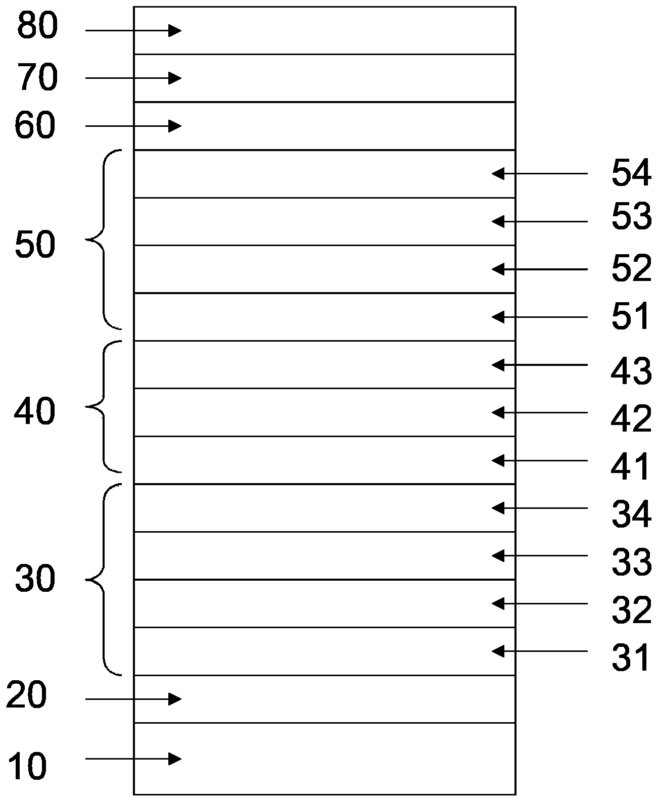
In
Das Substrat 10 kann als Trägerelement dienen und beispielsweise aus Glas, Quarz und/oder einem Halbleitermaterial gebildet sein. Alternativ kann das Substrat 10 auch eine Kunststofffolie oder ein Laminat aus mehreren Kunststofffolien sein.The
Das Bauelement in
Die erste Elektrode 20 kann als Anode oder Kathode ausgebildet sein und kann als Material beispielsweise ITO aufweisen. Wenn das Bauelement als Bottom-Emitter ausgebildet sein soll, sind Substrat 10 und erste Elektrode 20 transluzent. Für den Fall, dass das Bauelement als Top-Emitter ausgebildet sein soll, kann die erste Elektrode 20 bevorzugt auch reflektierend ausgebildet sein. Die zweite Elektrode 60 ist als Kathode oder Anode ausgebildet und kann beispielsweise ein Metall, oder ein TCO aufweisen. Auch die zweite Elektrode 60 kann transluzent ausgebildet sein, wenn das Bauelement als Top-Emitter ausgebildet ist.The
Die Barrieredünnschicht 70 schützt die organischen Schichten vor schädigenden Materialien aus der Umgebung wie beispielsweise Feuchtigkeit und/oder Sauerstoff und/oder anderen korrosiven Substanzen wie etwa Schwefelwasserstoff. Dazu kann die Barrieredünnschicht 70 eine oder mehrere dünne Schichten aufweisen, die beispielsweise mittels eines Atomlagenabscheideverfahrens aufgebracht sind und die beispielsweise eines oder mehrere der Materialien Aluminiumoxid, Zinkoxid, Zirkoniumoxid, Titanoxid, Hafniumoxid, Lantanoxid und Tantaloxid aufweisen. Die Barrieredünnschicht 70 weist weiterhin einen mechanischen Schutz in Form der Verkapselung 80 auf, die beispielsweise als Kunststoffschicht und/oder als auflaminierte Glasschicht ausgebildet ist, wodurch beispielsweise ein Kratzschutz erreicht werden kann.The barrier
Die Emissionsschichten 33 und 52 weisen beispielsweise ein im allgemeinen Teil genanntes elektrolumineszierendes Material auf. Diese können entweder gleich oder verschieden ausgewählt sein. Weiterhin können Ladungsträgerblockierschichten (hier nicht gezeigt) vorgesehen sein, zwischen denen die organischen Licht emittierenden Emissionsschichten 33 und 52 angeordnet sind.The emission layers 33 and 52 comprise, for example, an electroluminescent material mentioned in the general part. These can be selected either the same or different. Furthermore, charge carrier blocking layers (not shown here) can be provided, between which the organic light-emitting emission layers 33 and 52 are arranged.
Beispielsweise kann als Ladungsträgerblockierschicht eine Löcherblockierschicht vorhanden sein, die ein Material aufweist, das aus einer Gruppe ausgewählt ist, die 2,2',2" -(1,3,5-Benzinetriyl)-tris(1-phenyl-1-H-benzimidazol), 2-(4-Biphenylyl)-5-(4-tert-butylphenyl)-1,3,4-oxadiazol, 2,9-Dimethyl-4,7-diphenyl-1,10-phenanthroline (BCP), 8-Hydroxyquinolinolato-lithium, 4-(Naphthalen-1-yl)-3,5-diphenyl-4H-1,2,4-triazol, 1,3-Bis[2-(2,2'-bipyridine-6-yl)-1,3,4-oxadiazo-5-yl]benzol, 4,7-Diphenyl-1,10-phenanthrolin (BPhen)l 3-(4-Biphenylyl)-4-phenyl-5-tert-butylphenyl-1,2,4-triazol, Bis(2-methyl-8-quinolinolate)-4- (phenylphenolato) aluminium, 6,6'-Bis[5-(biphenyl-4-yl)-1,3,4-oxadiazo-2-yl]-2,2'-bipyridyl, 2-phenyl-9,10-di(naphthalen-2-yl)-anthracen, 2,7-Bis[2-(2,2'-bipyridine-6-yl)-1,3,4-oxadiazo-5-yl]-9,9-dimethylfluoren, 1,3-Bis[2-(4-tert-butylphenyl)-1,3,4-oxadiazo-5-yl]benzol, 2-(naphthalen-2-yl)-4,7-diphenyl-1,10-phenanthrolin, 2,9-Bis(naphthalen-2-yl)-4,7-diphenyl-1,10-phenanthrolin, Tris(2,4,6-trimethyl-3-(pyridin-3-yl)phenyl)boran, 1-methyl-2-(4-(naphthalen-2-yl)phenyl)-1H-imidazo[4,5-f][1,10]phenanthrolin, Phenyl-dipyrenylphosphine oxid, Naphtahlintetracarbonsäuredianhydrid und dessen Imide Perylentetracarbonsäuredianhydrid und dessen Imide Materialien basierend auf Silolen mit einer Silacyclopentadieneinheit, sowie Mischungen daraus umfasst.For example, a hole blocking layer may be present as the charge carrier blocking layer, which comprises a material selected from a group consisting of 2,2',2"-(1,3,5-benzinetriyl)-tris(1-phenyl-1-H-benzimidazole), 2-(4-biphenylyl)-5-(4-tert-butylphenyl)-1,3,4-oxadiazole, 2,9-dimethyl-4,7-diphenyl-1,10-phenanthroline (BCP), 8-hydroxyquinolinolato-lithium, 4-(naphthalen-1-yl)-3,5-diphenyl-4H-1,2,4-triazole, 1,3-bis[2-(2,2'-bipyridine-6-yl)-1,3,4-oxadiazo-5-yl]benzene, 4,7-diphenyl-1,10-phenanthroline (BPhen)l 3-(4-Biphenylyl)-4-phenyl-5-tert-butylphenyl-1,2,4-triazol, Bis(2-methyl-8-quinolinolate)-4- (phenylphenolato) aluminium, 6,6'-Bis[5-(biphenyl-4-yl)-1,3,4-oxadiazo-2-yl]-2,2'-bipyridyl, 2-phenyl-9,10-di(naphthalen-2-yl)-anthracen, 2,7-Bis[2-(2,2'-bipyridine-6-yl)-1,3,4-oxadiazo-5-yl]-9,9-dimethylfluoren, 1,3-Bis[2-(4-tert-butylphenyl)-1,3,4-oxadiazo-5-yl]benzol, 2-(naphthalen-2-yl)-4,7-diphenyl-1,10-phenanthrolin, 2,9-bis(naphthalen-2-yl)-4,7-diphenyl-1,10-phenanthroline, tris(2,4,6-trimethyl-3-(pyridin-3-yl)phenyl)borane, 1-methyl-2-(4-(naphthalen-2-yl)phenyl)-1H-imidazo[4,5-f][1,10]phenanthroline, phenyl-dipyrenylphosphine oxide, naphthalenetetracarboxylic dianhydride and its imides, perylenetetracarboxylic dianhydride and its imides, materials based on siloles having a silacyclopentadiene unit, and mixtures thereof.
Weiterhin kann als Ladungsträgerblockierschicht eine Elektronenblockierschicht vorhanden sein, die ein Material aufweist, das aus einer Gruppe ausgewählt ist, die NPB (N,N'-Bis(naphthalen-1-yl)-N,N'-bis(phenyl)-benzidin), beta-NPB N,N'-Bis(naphthalen-2-yl)-N,N'-bis(phenyl)-benzidin), TPD (N,N'-Bis(3-methylphenyl)-N,N'-bis(phenyl)-benzidin), Spiro TPD (N,N'-Bis(3-methylphenyl)-N,N'-bis(phenyl)-benzidin), Spiro-NPB (N,N'-Bis(naphthalen-1-yl)-N,N'-bis(phenyl)-spiro),
DMFL-TPD N,N'-Bis(3-methylphenyl)-N,N'-bis(phenyl)-9,9-dimethyl-fluoren),
DMFL-NPB (N,N'-Bis(naphthalen-1-yl)-N,N'-bis(phenyl)-9,9-dimethyl-fluoren),
DPFL-TPD (N,N'-Bis(3-methylphenyl)-N,N'-bis(phenyl)-9,9-diphenyl-fluoren),
DPFL-NPB (N,N'-Bis(naphthalen-1-yl)-N,N'-bis(phenyl)-9,9-diphenyl-fluoren),
Spiro-TAD (2,2',7,7'-Tetrakis(n,n-diphenylamino)- 9,9 ‚-spirobifluoren),
9,9-Bis[4-(N,N-bis-biphenyl-4-yl-amino)phenyl]-9H-fluoren, 9,9-Bis[4-(N,N-bis-naphthalen-2-yl-amino)phenyl]-9H-fluoren, 9,9-Bis[4-(N,N‘-bis-naphthalen-2-yl-N,N'-bis-phenyl-amino)-phenyl]-9H-fluor,
N,N'-bis (phenanthren-9-yl)-N,N'-bis (phenyl)-benzidin, 2,7-Bis[N,N-bis(9,9-spiro-bifluorene-2-yl)-amino]-9,9-spiro-bifluoren,
2,2'-Bis[N,N-bis (biphenyl-4-yl) amino] 9, 9-spiro-bifluoren, 2,2'-Bis(N,N-di-phenyl-amino)9,9-spiro-bifluoren, Di-[4-(N,N-ditolyl-amino)-phenyl]cyclohexan, 2,2',7,7'-tetra(N, N-di-tolyl)amino-spiro-bifluoren, N,N,N',N'-tetra-naphthalen-2-yl-benzidin,
sowie Mischungen daraus umfasst.Furthermore, an electron blocking layer can be present as the charge carrier blocking layer, which comprises a material selected from a group consisting of NPB (N,N'-bis(naphthalen-1-yl)-N,N'-bis(phenyl)benzidine), beta-NPB N,N'-bis(naphthalen-2-yl)-N,N'-bis(phenyl)benzidine), TPD (N,N'-bis(3-methylphe nyl)-N,N'-bis(phenyl)-benzidine), Spiro TPD (N,N'-bis(3-methylphenyl)-N,N'-bis(phenyl)-benzidine), Spiro-NPB (N,N'-bis(naphthalen-1-yl)-N,N'-bis(phenyl)-spiro),
DMFL-TPD N,N'-Bis(3-methylphenyl)-N,N'-bis(phenyl)-9,9-dimethylfluorene),
DMFL-NPB (N,N'-bis(naphthalen-1-yl)-N,N'-bis(phenyl)-9,9-dimethylfluorene),
DPFL-TPD (N,N'-Bis(3-methylphenyl)-N,N'-bis(phenyl)-9,9-diphenyl-fluorene),
DPFL-NPB (N,N'-bis(naphthalen-1-yl)-N,N'-bis(phenyl)-9,9-diphenylfluorene),
Spiro-TAD (2,2',7,7'-Tetrakis(n,n-diphenylamino)-9,9'-spirobifluorene),
9,9-bis[4-(N,N-bis-biphenyl-4-yl-amino)phenyl]-9H-fluorene, 9,9-bis[4-(N,N-bis-naphthalen-2-yl-amino)phenyl]-9H-fluorene, 9,9-bis[4-(N,N'-bis-naphthalen-2-yl-N,N'-bis-phenyl-amino)-phenyl]-9H-fluor,
N,N'-bis(phenanthren-9-yl)-N,N'-bis(phenyl)-benzidine, 2,7-bis[N,N-bis(9,9-spiro-bifluorene-2-yl)-amino]-9,9-spiro-bifluorene,
2,2'-Bis[N,N-bis(biphenyl-4-yl)amino] 9, 9-spiro-bifluorene, 2,2'-Bis(N,N-di-phenyl-amino)9,9-spiro-bifluorene, di-[4-(N,N-ditolyl-amino)-phenyl]cyclohexane, 2,2',7,7'-tetra(N, N-di-tolyl)amino-spiro -bifluorene, N,N,N',N'-tetra-naphthalen-2-yl-benzidine,
and mixtures thereof.
Materialien für die Lochtransportschichten 32 und 51, für die Lochinjektionsschicht 31, für die Elektronentransportschichten 34 und 53 sowie für die Elektroneninjektionsschicht 54 können aus bekannten Materialien ausgewählt werden. Beispielsweise kann für die Lochtransportschichten 32 und 51 eines oder mehrere der Materialien ausgewählt werden, die oben bezüglich der ersten und zweiten lochtransportierenden Schicht angegeben sind. Weiterhin kann für die Elektronentransportschichten 34 und 53eines oder mehrere der Materialien ausgewählt werden, die oben bezüglich der elekronentransportierenden Schicht angegeben sind.Materials for the hole transport layers 32 and 51, for the
Der Ladungsträgererzeugungs-Schichtenstapel 40 enthält in dem Ausführungsbeispiel eine elektronentransportierende Schicht 41, welche als Matrixmaterial NET-18 und als Dotierstoff NDN-26 enthält und eine Dicke von beispielsweise etwa 5 nm oder 15 nm aufweist. Die lochtransportierende Schicht 43 weist als Material HAT-CN und als Schichtdicke beispielsweise etwa 5 nm oder 15 nm auf. Die Zwischenschicht 42 hat eine Dicke von etwa 4 nm und enthält als Material ein multinukleares Phthalocyanin-Derivat, beispielsweise ausgewählt aus den in den Strukturformeln IV, V, VI oder VII gezeigten Verbindungen.In the exemplary embodiment, the charge carrier
Eine alternative Ausführungsform des Ladungsträgererzeugungs-Schichtenstapel 40 ist in
Eine weitere Ausführungsform des Ladungsträgererzeugungs-Schichtenstapels 40 ist in
Ein Bauelement wie es in den
Anhand dieses Aufbaus wird in
Beim Einsatz von multinuklearen Phthalocyanin-Derivaten, wie beispielsweise den in den Strukturformeln IV bis VII dargestellten Verbindungen, anstelle von mononuklearen Phthalocyaninen kann bei gleicher Spannung der Tunnelstrom erhöht werden und der Ladungsträgererzeugungs-Schichtenstapel stabil bleiben, das heißt, dass eine hohe Spannungsstabilität beim Belastungstest bei hoher Temperatur zu verzeichnen ist. Weiterhin ist die Transmission im gelb-roten Spektralbereich vorteilhaft erhöht.When using multinuclear phthalocyanine derivatives, such as the compounds shown in structural formulas IV to VII, instead of mononuclear phthalocyanines, the tunnel current can be increased at the same voltage and the charge carrier generation layer stack can remain stable, which means that a high voltage stability is recorded during the stress test at high temperature. Furthermore, the transmission in the yellow-red spectral range is advantageously increased.
Dadurch, dass die vergrößerten multinuklearen Phthalocyanin-Derivate bei der Verdampfung als eine zusammenhängende Schicht abgeschieden werden können, kann die lochtransportierende Schicht 43, beispielsweise die HAT-CN Schicht, noch effektiver von der sehr reaktiven, gegebenenfalls n-dotierten elektronentransportierenden Schicht 41 getrennt werden.Because the enlarged multinuclear phthalocyanine derivatives can be deposited as a continuous layer during evaporation, the hole-transporting
Mittels Absorptionsspektren von verschiedenen Verbindungen, aus denen Zwischenschichten 42 gebildet werden können, können deren Absorptionseigenschaften verglichen werden.By means of absorption spectra of different compounds from which
Vergleicht man beispielsweise das Absorptionsspektrum von ZnPc (III) im Vergleich zu dem metallfreien H2Pc (IIIa), sieht man eine leicht herabgesetzte Absorption, insbesondere im Bereich zwischen 300 nm und 450 nm, des ZnPc gegenüber dem H2Pc, Weiterhin weist das H2Pc zwei charakteristische Übergänge des π-Elektronensystems bei etwa 650 nm und 700 nm auf, während das ZnPc einen charakteristischen Übergang aufweist, der zwischen den beiden Übergängen des H2Pc liegt.For example, if one compares the absorption spectrum of ZnPc (III) with that of the metal-free H 2 Pc (IIIa), one can see a slightly reduced absorption, especially in the range between 300 nm and 450 nm, of ZnPc compared to H 2 Pc. Furthermore, H 2 Pc has two characteristic transitions of the π-electron system at about 650 nm and 700 nm, while ZnPc has a characteristic transition that lies between the two transitions of H 2 Pc.
Das in Strukturformel V gezeigte ZnPc-ZnPc in Toluol zeigt im Vergleich zu dem in Strukturformel IV gezeigten H2Pc-H2Pc ebenfalls eine herabgesetzte Absorption in dem Bereich von 300 nm bis 800 nm. Die charakteristischen Übergänge des π-Elektronensystems des H2Pc-H2Pc liegen beide zwischen 600 nm und 650 nm, der charakteristische Übergang des ZnPc-ZnPc liegt dazwischen.The ZnPc-ZnPc in toluene shown in structural formula V also shows a reduced absorption in the range from 300 nm to 800 nm compared to the H 2 Pc-H 2 Pc shown in structural formula IV. The characteristic transitions of the π-electron system of the H 2 Pc-H 2 Pc are both between 600 nm and 650 nm, the characteristic transition of the ZnPc-ZnPc is in between.
Der Vergleich des Absorptionsverhaltens eines linearen trinuklearen Phthalocyanin-Derivats (VI) im Vergleich zu einem rechtwinklig anelierten trinuklearen Phthalocyanin-Derivats (VII), wobei beide Phthalocyanin-Derivate Zn-haltig sind, zeigt, dass die lineare Variante eine geringere Absorption in dem Bereich etwa 400 bis 800 nm zeigt als die rechtwinklig anelierte Variante und zudem einen charakteristischen Übergang des π-Elektronensystems bei etwa 950 nm aufweist, während die rechtwinklige Variante zwei Übergänge bei etwa 850 nm und 900 nm zeigt.The comparison of the absorption behavior of a linear trinuclear phthalocyanine derivative (VI) compared to a right-angle fused trinuclear phthalocyanine derivative (VII), both phthalocyanine derivatives containing Zn, shows that the linear variant shows a lower absorption in the range of about 400 to 800 nm than the right-angle fused variant and also shows a characteristic transition of the π-electron system at about 950 nm, while the right-angle variant shows two transitions at about 850 nm and 900 nm.
Claims (15)
Priority Applications (3)
| Application Number | Priority Date | Filing Date | Title |
|---|---|---|---|
| DE102013107113.9A DE102013107113B4 (en) | 2013-07-05 | 2013-07-05 | Organic light-emitting device and method for producing an organic light-emitting device |
| PCT/EP2014/063835 WO2015000835A1 (en) | 2013-07-05 | 2014-06-30 | Organic light-emitting component and method for producing an organic light-emitting component |
| US14/900,151 US20160155991A1 (en) | 2013-07-05 | 2014-06-30 | Organic Light-Emitting Component and Method for Producing an Organic Light-Emitting Component |
Applications Claiming Priority (1)
| Application Number | Priority Date | Filing Date | Title |
|---|---|---|---|
| DE102013107113.9A DE102013107113B4 (en) | 2013-07-05 | 2013-07-05 | Organic light-emitting device and method for producing an organic light-emitting device |
Publications (2)
| Publication Number | Publication Date |
|---|---|
| DE102013107113A1 DE102013107113A1 (en) | 2015-01-08 |
| DE102013107113B4 true DE102013107113B4 (en) | 2024-08-29 |
Family
ID=51062812
Family Applications (1)
| Application Number | Title | Priority Date | Filing Date |
|---|---|---|---|
| DE102013107113.9A Active DE102013107113B4 (en) | 2013-07-05 | 2013-07-05 | Organic light-emitting device and method for producing an organic light-emitting device |
Country Status (3)
| Country | Link |
|---|---|
| US (1) | US20160155991A1 (en) |
| DE (1) | DE102013107113B4 (en) |
| WO (1) | WO2015000835A1 (en) |
Families Citing this family (9)
| Publication number | Priority date | Publication date | Assignee | Title |
|---|---|---|---|---|
| DE102013017361B4 (en) | 2013-10-18 | 2023-05-04 | Pictiva Displays International Limited | Organic light emitting device and method for producing an organic light emitting device |
| DE102015108826B4 (en) * | 2015-06-03 | 2025-08-21 | Pictiva Displays International Limited | Organic light-emitting component and method for producing an organic light-emitting component |
| DE102015114084A1 (en) | 2015-08-25 | 2017-03-02 | Osram Oled Gmbh | Organic light emitting device and light |
| DE102015116389A1 (en) | 2015-09-28 | 2017-03-30 | Osram Oled Gmbh | Organic electronic device with carrier generation layer and use of a zinc complex as a p-type dopant in carrier generation layers |
| DE102015119994A1 (en) * | 2015-11-18 | 2017-05-18 | Osram Oled Gmbh | Method for producing a layer, use of the layer, method for producing an organic light-emitting component and organic light-emitting component |
| DE102016106917A1 (en) | 2016-04-14 | 2017-10-19 | Osram Oled Gmbh | Organic electronic component with carrier generation layer |
| DE102017101077B4 (en) | 2017-01-20 | 2025-06-26 | Pictiva Displays International Limited | Organic electronic component |
| WO2020063592A1 (en) * | 2018-09-29 | 2020-04-02 | Tcl集团股份有限公司 | Quantum dot light-emitting diode |
| CN111599929B (en) * | 2020-05-08 | 2024-11-26 | 义乌清越光电科技有限公司 | Organic light emitting diode and organic light emitting device |
Citations (3)
| Publication number | Priority date | Publication date | Assignee | Title |
|---|---|---|---|---|
| US5280183A (en) | 1988-05-31 | 1994-01-18 | Edison Polymer Innovation Corporation | Microelectronic device employing multiring phthalocyanine compound |
| WO2010066245A1 (en) | 2008-12-11 | 2010-06-17 | Osram Opto Semiconductors Gmbh | Organic light-emitting diode and luminaire |
| US20110240971A1 (en) | 2010-03-31 | 2011-10-06 | Semiconductor Energy Laboratory Co., Ltd. | Light-Emitting Element, Light-Emitting Device, Electronic Device, and Lighting Device |
Family Cites Families (9)
| Publication number | Priority date | Publication date | Assignee | Title |
|---|---|---|---|---|
| JPH0730080B2 (en) * | 1987-08-12 | 1995-04-05 | 理化学研究所 | Phthalocyanine derivative |
| US6268695B1 (en) * | 1998-12-16 | 2001-07-31 | Battelle Memorial Institute | Environmental barrier material for organic light emitting device and method of making |
| JP4513060B2 (en) * | 2004-09-06 | 2010-07-28 | 富士電機ホールディングス株式会社 | Organic EL device |
| US20080061685A1 (en) * | 2006-08-24 | 2008-03-13 | Chesterfield Reid J | Organic electronic devices |
| US8603642B2 (en) * | 2009-05-13 | 2013-12-10 | Global Oled Technology Llc | Internal connector for organic electronic devices |
| KR101089715B1 (en) * | 2009-11-05 | 2011-12-07 | 한국기계연구원 | Multilayer thin film encapsulation film and manufacturing method thereof |
| WO2011162105A1 (en) * | 2010-06-25 | 2011-12-29 | Semiconductor Energy Laboratory Co., Ltd. | Light-emitting element, light-emitting device, display, and electronic device |
| KR101880183B1 (en) * | 2011-02-11 | 2018-07-19 | 가부시키가이샤 한도오따이 에네루기 켄큐쇼 | Light-emitting device and display device |
| JP2012204110A (en) * | 2011-03-24 | 2012-10-22 | Sony Corp | Display element, display device, and electronic apparatus |
-
2013
- 2013-07-05 DE DE102013107113.9A patent/DE102013107113B4/en active Active
-
2014
- 2014-06-30 WO PCT/EP2014/063835 patent/WO2015000835A1/en not_active Ceased
- 2014-06-30 US US14/900,151 patent/US20160155991A1/en not_active Abandoned
Patent Citations (3)
| Publication number | Priority date | Publication date | Assignee | Title |
|---|---|---|---|---|
| US5280183A (en) | 1988-05-31 | 1994-01-18 | Edison Polymer Innovation Corporation | Microelectronic device employing multiring phthalocyanine compound |
| WO2010066245A1 (en) | 2008-12-11 | 2010-06-17 | Osram Opto Semiconductors Gmbh | Organic light-emitting diode and luminaire |
| US20110240971A1 (en) | 2010-03-31 | 2011-10-06 | Semiconductor Energy Laboratory Co., Ltd. | Light-Emitting Element, Light-Emitting Device, Electronic Device, and Lighting Device |
Non-Patent Citations (3)
| Title |
|---|
| M. Kröger et al., Phys. Rev. B 75, 235321 (2007) |
| R. Meerheim et al., Appl. Phys. Lett. 89, 061111 (2006) |
| T.-W. Lee et al., APL 92, 043301 (2008) |
Also Published As
| Publication number | Publication date |
|---|---|
| DE102013107113A1 (en) | 2015-01-08 |
| US20160155991A1 (en) | 2016-06-02 |
| WO2015000835A1 (en) | 2015-01-08 |
Similar Documents
| Publication | Publication Date | Title |
|---|---|---|
| DE102013017361B4 (en) | Organic light emitting device and method for producing an organic light emitting device | |
| DE102013107113B4 (en) | Organic light-emitting device and method for producing an organic light-emitting device | |
| EP1488468B1 (en) | Transparent, thermally stable light-emitting component comprising organic layers | |
| EP1336208B1 (en) | Light emitting component comprising organic layers | |
| DE102012214021B4 (en) | Optoelectronic component and method for producing an optoelectronic component | |
| EP2652809B1 (en) | Organic light emitting device and use of a copper complex in a charge transfer layer | |
| EP2652811B1 (en) | Optoelectronic component, and use of a copper complex in a charge generation layer sequence | |
| DE102011007052A1 (en) | Optoelectronic component and use of a copper complex as a dopant for doping a layer | |
| WO2017032802A1 (en) | Organic light-emitting component and lamp | |
| WO2015124636A2 (en) | Organic optoelectronic component and method for producing an organic optoelectronic component | |
| DE112014007311B9 (en) | Organic light-emitting device | |
| DE102010056519A1 (en) | Optoelectronic component with doped layers | |
| DE102012208235B4 (en) | Optoelectronic component and method for producing an optoelectronic component | |
| WO2017178473A1 (en) | Organic electronic component having a charge-carrier generation layer | |
| DE102014117011B4 (en) | Process for the production of an organic light-emitting component | |
| DE102015102371B4 (en) | Organic light emitting device | |
| WO2016030331A1 (en) | Organic light-emitting component and method for producing an organic light-emitting component | |
| DE102012025879B3 (en) | Optoelectronic component and method for producing an optoelectronic component | |
| DE102015017493B4 (en) | Organic light-emitting component | |
| WO2017085204A1 (en) | Method for producing a layer, use of the layer, method for producing an organic light-emitting component, and organic light-emitting component | |
| WO2016150687A1 (en) | Method for producing an organic charge-carrier generating layer and an organic light-emitting component with an organic charge-carrier generating layer |
Legal Events
| Date | Code | Title | Description |
|---|---|---|---|
| R163 | Identified publications notified | ||
| R082 | Change of representative |
Representative=s name: EPPING HERMANN FISCHER, PATENTANWALTSGESELLSCH, DE |
|
| R081 | Change of applicant/patentee |
Owner name: OSRAM OLED GMBH, DE Free format text: FORMER OWNER: OSRAM OPTO SEMICONDUCTORS GMBH, 93055 REGENSBURG, DE Effective date: 20150209 |
|
| R082 | Change of representative |
Representative=s name: EPPING HERMANN FISCHER, PATENTANWALTSGESELLSCH, DE Effective date: 20150209 Representative=s name: EPPING HERMANN FISCHER PATENTANWALTSGESELLSCHA, DE Effective date: 20150209 |
|
| R012 | Request for examination validly filed | ||
| R081 | Change of applicant/patentee |
Owner name: PICTIVA DISPLAYS INTERNATIONAL LIMITED, IE Free format text: FORMER OWNER: OSRAM OLED GMBH, 93049 REGENSBURG, DE |
|
| R082 | Change of representative |
Representative=s name: EPPING HERMANN FISCHER PATENTANWALTSGESELLSCHA, DE |
|
| R079 | Amendment of ipc main class |
Free format text: PREVIOUS MAIN CLASS: H01L0051520000 Ipc: H10K0050800000 |
|
| R079 | Amendment of ipc main class |
Free format text: PREVIOUS MAIN CLASS: H10K0050800000 Ipc: H10K0050110000 |
|
| R016 | Response to examination communication | ||
| R018 | Grant decision by examination section/examining division | ||
| R079 | Amendment of ipc main class |
Free format text: PREVIOUS MAIN CLASS: H10K0050110000 Ipc: H10K0050130000 |
|
| R020 | Patent grant now final |