DE102013004558B4 - Method for producing a surface-strained sapphire disk, surface-strained sapphire disk and electrical device with a transparent cover - Google Patents
Method for producing a surface-strained sapphire disk, surface-strained sapphire disk and electrical device with a transparent cover Download PDFInfo
- Publication number
- DE102013004558B4 DE102013004558B4 DE102013004558.4A DE102013004558A DE102013004558B4 DE 102013004558 B4 DE102013004558 B4 DE 102013004558B4 DE 102013004558 A DE102013004558 A DE 102013004558A DE 102013004558 B4 DE102013004558 B4 DE 102013004558B4
- Authority
- DE
- Germany
- Prior art keywords
- layer
- sapphire
- substrate
- strained
- disk
- Prior art date
- Legal status (The legal status is an assumption and is not a legal conclusion. Google has not performed a legal analysis and makes no representation as to the accuracy of the status listed.)
- Expired - Fee Related
Links
- 229910052594 sapphire Inorganic materials 0.000 title claims abstract description 98
- 239000010980 sapphire Substances 0.000 title claims abstract description 98
- 238000004519 manufacturing process Methods 0.000 title claims abstract description 7
- 239000000758 substrate Substances 0.000 claims abstract description 83
- 238000000576 coating method Methods 0.000 claims abstract description 23
- 238000000034 method Methods 0.000 claims abstract description 21
- GQPLMRYTRLFLPF-UHFFFAOYSA-N Nitrous Oxide Chemical compound [O-][N+]#N GQPLMRYTRLFLPF-UHFFFAOYSA-N 0.000 claims abstract description 13
- 239000011248 coating agent Substances 0.000 claims abstract description 13
- JLTRXTDYQLMHGR-UHFFFAOYSA-N trimethylaluminium Chemical compound C[Al](C)C JLTRXTDYQLMHGR-UHFFFAOYSA-N 0.000 claims abstract description 13
- 239000007789 gas Substances 0.000 claims abstract description 10
- 238000006243 chemical reaction Methods 0.000 claims abstract description 8
- 229910018072 Al 2 O 3 Inorganic materials 0.000 claims abstract description 5
- 238000005268 plasma chemical vapour deposition Methods 0.000 claims abstract description 4
- 238000000623 plasma-assisted chemical vapour deposition Methods 0.000 claims abstract description 4
- IJGRMHOSHXDMSA-UHFFFAOYSA-N Atomic nitrogen Chemical compound N#N IJGRMHOSHXDMSA-UHFFFAOYSA-N 0.000 claims description 8
- OKTJSMMVPCPJKN-UHFFFAOYSA-N Carbon Chemical compound [C] OKTJSMMVPCPJKN-UHFFFAOYSA-N 0.000 claims description 4
- UFHFLCQGNIYNRP-UHFFFAOYSA-N Hydrogen Chemical compound [H][H] UFHFLCQGNIYNRP-UHFFFAOYSA-N 0.000 claims description 4
- 229910052799 carbon Inorganic materials 0.000 claims description 4
- 239000001257 hydrogen Substances 0.000 claims description 4
- 229910052739 hydrogen Inorganic materials 0.000 claims description 4
- 229910052757 nitrogen Inorganic materials 0.000 claims description 4
- 239000001272 nitrous oxide Substances 0.000 claims description 3
- 230000005670 electromagnetic radiation Effects 0.000 claims description 2
- 238000002834 transmittance Methods 0.000 claims description 2
- 229960001730 nitrous oxide Drugs 0.000 abstract description 5
- 235000013842 nitrous oxide Nutrition 0.000 abstract description 3
- TWNQGVIAIRXVLR-UHFFFAOYSA-N oxo(oxoalumanyloxy)alumane Chemical compound O=[Al]O[Al]=O TWNQGVIAIRXVLR-UHFFFAOYSA-N 0.000 description 12
- PNEYBMLMFCGWSK-UHFFFAOYSA-N aluminium oxide Inorganic materials [O-2].[O-2].[O-2].[Al+3].[Al+3] PNEYBMLMFCGWSK-UHFFFAOYSA-N 0.000 description 9
- 229910052581 Si3N4 Inorganic materials 0.000 description 8
- HQVNEWCFYHHQES-UHFFFAOYSA-N silicon nitride Chemical compound N12[Si]34N5[Si]62N3[Si]51N64 HQVNEWCFYHHQES-UHFFFAOYSA-N 0.000 description 8
- 238000005452 bending Methods 0.000 description 6
- 230000003287 optical effect Effects 0.000 description 6
- 239000013078 crystal Substances 0.000 description 5
- 238000000137 annealing Methods 0.000 description 4
- 238000001816 cooling Methods 0.000 description 3
- 230000007547 defect Effects 0.000 description 3
- 230000000694 effects Effects 0.000 description 3
- 239000012495 reaction gas Substances 0.000 description 3
- MWUXSHHQAYIFBG-UHFFFAOYSA-N Nitric oxide Chemical compound O=[N] MWUXSHHQAYIFBG-UHFFFAOYSA-N 0.000 description 2
- MXRIRQGCELJRSN-UHFFFAOYSA-N O.O.O.[Al] Chemical compound O.O.O.[Al] MXRIRQGCELJRSN-UHFFFAOYSA-N 0.000 description 2
- 230000001419 dependent effect Effects 0.000 description 2
- 238000002474 experimental method Methods 0.000 description 2
- 239000000463 material Substances 0.000 description 2
- 238000002156 mixing Methods 0.000 description 2
- 239000000203 mixture Substances 0.000 description 2
- 238000009832 plasma treatment Methods 0.000 description 2
- 239000000126 substance Substances 0.000 description 2
- 238000001429 visible spectrum Methods 0.000 description 2
- 150000004703 alkoxides Chemical class 0.000 description 1
- XAGFODPZIPBFFR-UHFFFAOYSA-N aluminium Chemical compound [Al] XAGFODPZIPBFFR-UHFFFAOYSA-N 0.000 description 1
- 229910052782 aluminium Inorganic materials 0.000 description 1
- 230000005540 biological transmission Effects 0.000 description 1
- 239000000919 ceramic Substances 0.000 description 1
- 239000007795 chemical reaction product Substances 0.000 description 1
- 238000005056 compaction Methods 0.000 description 1
- 230000008878 coupling Effects 0.000 description 1
- 238000010168 coupling process Methods 0.000 description 1
- 238000005859 coupling reaction Methods 0.000 description 1
- 238000000151 deposition Methods 0.000 description 1
- 230000008021 deposition Effects 0.000 description 1
- 238000009792 diffusion process Methods 0.000 description 1
- 239000011521 glass Substances 0.000 description 1
- 238000010348 incorporation Methods 0.000 description 1
- 238000010849 ion bombardment Methods 0.000 description 1
- 238000004544 sputter deposition Methods 0.000 description 1
- 238000005728 strengthening Methods 0.000 description 1
- 238000009997 thermal pre-treatment Methods 0.000 description 1
- 238000005019 vapor deposition process Methods 0.000 description 1
Images

Classifications
-
- C—CHEMISTRY; METALLURGY
- C23—COATING METALLIC MATERIAL; COATING MATERIAL WITH METALLIC MATERIAL; CHEMICAL SURFACE TREATMENT; DIFFUSION TREATMENT OF METALLIC MATERIAL; COATING BY VACUUM EVAPORATION, BY SPUTTERING, BY ION IMPLANTATION OR BY CHEMICAL VAPOUR DEPOSITION, IN GENERAL; INHIBITING CORROSION OF METALLIC MATERIAL OR INCRUSTATION IN GENERAL
- C23C—COATING METALLIC MATERIAL; COATING MATERIAL WITH METALLIC MATERIAL; SURFACE TREATMENT OF METALLIC MATERIAL BY DIFFUSION INTO THE SURFACE, BY CHEMICAL CONVERSION OR SUBSTITUTION; COATING BY VACUUM EVAPORATION, BY SPUTTERING, BY ION IMPLANTATION OR BY CHEMICAL VAPOUR DEPOSITION, IN GENERAL
- C23C16/00—Chemical coating by decomposition of gaseous compounds, without leaving reaction products of surface material in the coating, i.e. chemical vapour deposition [CVD] processes
- C23C16/44—Chemical coating by decomposition of gaseous compounds, without leaving reaction products of surface material in the coating, i.e. chemical vapour deposition [CVD] processes characterised by the method of coating
- C23C16/50—Chemical coating by decomposition of gaseous compounds, without leaving reaction products of surface material in the coating, i.e. chemical vapour deposition [CVD] processes characterised by the method of coating using electric discharges
- C23C16/513—Chemical coating by decomposition of gaseous compounds, without leaving reaction products of surface material in the coating, i.e. chemical vapour deposition [CVD] processes characterised by the method of coating using electric discharges using plasma jets
-
- C—CHEMISTRY; METALLURGY
- C03—GLASS; MINERAL OR SLAG WOOL
- C03C—CHEMICAL COMPOSITION OF GLASSES, GLAZES OR VITREOUS ENAMELS; SURFACE TREATMENT OF GLASS; SURFACE TREATMENT OF FIBRES OR FILAMENTS MADE FROM GLASS, MINERALS OR SLAGS; JOINING GLASS TO GLASS OR OTHER MATERIALS
- C03C17/00—Surface treatment of glass, not in the form of fibres or filaments, by coating
- C03C17/22—Surface treatment of glass, not in the form of fibres or filaments, by coating with other inorganic material
- C03C17/23—Oxides
- C03C17/245—Oxides by deposition from the vapour phase
-
- C—CHEMISTRY; METALLURGY
- C23—COATING METALLIC MATERIAL; COATING MATERIAL WITH METALLIC MATERIAL; CHEMICAL SURFACE TREATMENT; DIFFUSION TREATMENT OF METALLIC MATERIAL; COATING BY VACUUM EVAPORATION, BY SPUTTERING, BY ION IMPLANTATION OR BY CHEMICAL VAPOUR DEPOSITION, IN GENERAL; INHIBITING CORROSION OF METALLIC MATERIAL OR INCRUSTATION IN GENERAL
- C23C—COATING METALLIC MATERIAL; COATING MATERIAL WITH METALLIC MATERIAL; SURFACE TREATMENT OF METALLIC MATERIAL BY DIFFUSION INTO THE SURFACE, BY CHEMICAL CONVERSION OR SUBSTITUTION; COATING BY VACUUM EVAPORATION, BY SPUTTERING, BY ION IMPLANTATION OR BY CHEMICAL VAPOUR DEPOSITION, IN GENERAL
- C23C14/00—Coating by vacuum evaporation, by sputtering or by ion implantation of the coating forming material
- C23C14/06—Coating by vacuum evaporation, by sputtering or by ion implantation of the coating forming material characterised by the coating material
- C23C14/08—Oxides
- C23C14/081—Oxides of aluminium, magnesium or beryllium
-
- C—CHEMISTRY; METALLURGY
- C23—COATING METALLIC MATERIAL; COATING MATERIAL WITH METALLIC MATERIAL; CHEMICAL SURFACE TREATMENT; DIFFUSION TREATMENT OF METALLIC MATERIAL; COATING BY VACUUM EVAPORATION, BY SPUTTERING, BY ION IMPLANTATION OR BY CHEMICAL VAPOUR DEPOSITION, IN GENERAL; INHIBITING CORROSION OF METALLIC MATERIAL OR INCRUSTATION IN GENERAL
- C23C—COATING METALLIC MATERIAL; COATING MATERIAL WITH METALLIC MATERIAL; SURFACE TREATMENT OF METALLIC MATERIAL BY DIFFUSION INTO THE SURFACE, BY CHEMICAL CONVERSION OR SUBSTITUTION; COATING BY VACUUM EVAPORATION, BY SPUTTERING, BY ION IMPLANTATION OR BY CHEMICAL VAPOUR DEPOSITION, IN GENERAL
- C23C14/00—Coating by vacuum evaporation, by sputtering or by ion implantation of the coating forming material
- C23C14/22—Coating by vacuum evaporation, by sputtering or by ion implantation of the coating forming material characterised by the process of coating
- C23C14/34—Sputtering
-
- C—CHEMISTRY; METALLURGY
- C23—COATING METALLIC MATERIAL; COATING MATERIAL WITH METALLIC MATERIAL; CHEMICAL SURFACE TREATMENT; DIFFUSION TREATMENT OF METALLIC MATERIAL; COATING BY VACUUM EVAPORATION, BY SPUTTERING, BY ION IMPLANTATION OR BY CHEMICAL VAPOUR DEPOSITION, IN GENERAL; INHIBITING CORROSION OF METALLIC MATERIAL OR INCRUSTATION IN GENERAL
- C23C—COATING METALLIC MATERIAL; COATING MATERIAL WITH METALLIC MATERIAL; SURFACE TREATMENT OF METALLIC MATERIAL BY DIFFUSION INTO THE SURFACE, BY CHEMICAL CONVERSION OR SUBSTITUTION; COATING BY VACUUM EVAPORATION, BY SPUTTERING, BY ION IMPLANTATION OR BY CHEMICAL VAPOUR DEPOSITION, IN GENERAL
- C23C14/00—Coating by vacuum evaporation, by sputtering or by ion implantation of the coating forming material
- C23C14/58—After-treatment
- C23C14/5806—Thermal treatment
- C23C14/582—Thermal treatment using electron bombardment
-
- C—CHEMISTRY; METALLURGY
- C23—COATING METALLIC MATERIAL; COATING MATERIAL WITH METALLIC MATERIAL; CHEMICAL SURFACE TREATMENT; DIFFUSION TREATMENT OF METALLIC MATERIAL; COATING BY VACUUM EVAPORATION, BY SPUTTERING, BY ION IMPLANTATION OR BY CHEMICAL VAPOUR DEPOSITION, IN GENERAL; INHIBITING CORROSION OF METALLIC MATERIAL OR INCRUSTATION IN GENERAL
- C23C—COATING METALLIC MATERIAL; COATING MATERIAL WITH METALLIC MATERIAL; SURFACE TREATMENT OF METALLIC MATERIAL BY DIFFUSION INTO THE SURFACE, BY CHEMICAL CONVERSION OR SUBSTITUTION; COATING BY VACUUM EVAPORATION, BY SPUTTERING, BY ION IMPLANTATION OR BY CHEMICAL VAPOUR DEPOSITION, IN GENERAL
- C23C16/00—Chemical coating by decomposition of gaseous compounds, without leaving reaction products of surface material in the coating, i.e. chemical vapour deposition [CVD] processes
- C23C16/22—Chemical coating by decomposition of gaseous compounds, without leaving reaction products of surface material in the coating, i.e. chemical vapour deposition [CVD] processes characterised by the deposition of inorganic material, other than metallic material
- C23C16/30—Deposition of compounds, mixtures or solid solutions, e.g. borides, carbides, nitrides
- C23C16/40—Oxides
- C23C16/403—Oxides of aluminium, magnesium or beryllium
-
- C—CHEMISTRY; METALLURGY
- C30—CRYSTAL GROWTH
- C30B—SINGLE-CRYSTAL GROWTH; UNIDIRECTIONAL SOLIDIFICATION OF EUTECTIC MATERIAL OR UNIDIRECTIONAL DEMIXING OF EUTECTOID MATERIAL; REFINING BY ZONE-MELTING OF MATERIAL; PRODUCTION OF A HOMOGENEOUS POLYCRYSTALLINE MATERIAL WITH DEFINED STRUCTURE; SINGLE CRYSTALS OR HOMOGENEOUS POLYCRYSTALLINE MATERIAL WITH DEFINED STRUCTURE; AFTER-TREATMENT OF SINGLE CRYSTALS OR A HOMOGENEOUS POLYCRYSTALLINE MATERIAL WITH DEFINED STRUCTURE; APPARATUS THEREFOR
- C30B29/00—Single crystals or homogeneous polycrystalline material with defined structure characterised by the material or by their shape
- C30B29/10—Inorganic compounds or compositions
- C30B29/16—Oxides
- C30B29/20—Aluminium oxides
-
- Y—GENERAL TAGGING OF NEW TECHNOLOGICAL DEVELOPMENTS; GENERAL TAGGING OF CROSS-SECTIONAL TECHNOLOGIES SPANNING OVER SEVERAL SECTIONS OF THE IPC; TECHNICAL SUBJECTS COVERED BY FORMER USPC CROSS-REFERENCE ART COLLECTIONS [XRACs] AND DIGESTS
- Y10—TECHNICAL SUBJECTS COVERED BY FORMER USPC
- Y10T—TECHNICAL SUBJECTS COVERED BY FORMER US CLASSIFICATION
- Y10T428/00—Stock material or miscellaneous articles
- Y10T428/24—Structurally defined web or sheet [e.g., overall dimension, etc.]
- Y10T428/24942—Structurally defined web or sheet [e.g., overall dimension, etc.] including components having same physical characteristic in differing degree
-
- Y—GENERAL TAGGING OF NEW TECHNOLOGICAL DEVELOPMENTS; GENERAL TAGGING OF CROSS-SECTIONAL TECHNOLOGIES SPANNING OVER SEVERAL SECTIONS OF THE IPC; TECHNICAL SUBJECTS COVERED BY FORMER USPC CROSS-REFERENCE ART COLLECTIONS [XRACs] AND DIGESTS
- Y10—TECHNICAL SUBJECTS COVERED BY FORMER USPC
- Y10T—TECHNICAL SUBJECTS COVERED BY FORMER US CLASSIFICATION
- Y10T428/00—Stock material or miscellaneous articles
- Y10T428/26—Web or sheet containing structurally defined element or component, the element or component having a specified physical dimension
- Y10T428/263—Coating layer not in excess of 5 mils thick or equivalent
- Y10T428/264—Up to 3 mils
- Y10T428/265—1 mil or less
-
- Y—GENERAL TAGGING OF NEW TECHNOLOGICAL DEVELOPMENTS; GENERAL TAGGING OF CROSS-SECTIONAL TECHNOLOGIES SPANNING OVER SEVERAL SECTIONS OF THE IPC; TECHNICAL SUBJECTS COVERED BY FORMER USPC CROSS-REFERENCE ART COLLECTIONS [XRACs] AND DIGESTS
- Y10—TECHNICAL SUBJECTS COVERED BY FORMER USPC
- Y10T—TECHNICAL SUBJECTS COVERED BY FORMER US CLASSIFICATION
- Y10T428/00—Stock material or miscellaneous articles
- Y10T428/26—Web or sheet containing structurally defined element or component, the element or component having a specified physical dimension
- Y10T428/266—Web or sheet containing structurally defined element or component, the element or component having a specified physical dimension of base or substrate
Landscapes
- Chemical & Material Sciences (AREA)
- Engineering & Computer Science (AREA)
- Materials Engineering (AREA)
- Organic Chemistry (AREA)
- Metallurgy (AREA)
- Chemical Kinetics & Catalysis (AREA)
- Mechanical Engineering (AREA)
- General Chemical & Material Sciences (AREA)
- Inorganic Chemistry (AREA)
- Physics & Mathematics (AREA)
- Plasma & Fusion (AREA)
- Crystallography & Structural Chemistry (AREA)
- Life Sciences & Earth Sciences (AREA)
- Geochemistry & Mineralogy (AREA)
- Thermal Sciences (AREA)
- Physical Vapour Deposition (AREA)
- Crystals, And After-Treatments Of Crystals (AREA)
- Chemical Vapour Deposition (AREA)
- Magnetic Record Carriers (AREA)
- Manufacturing Optical Record Carriers (AREA)
Abstract
Verfahren zur Herstellung einer Saphirscheibe mit den Schritten:
– Bereitstellen eines planaren Saphirsubstrats (10),
– Beschichten zumindest einer Oberfläche (11) des Substrats (10) mit einer das Substrat (10) verspannenden Schicht (12), indem die Schicht (12) mittels eines plasmagestützten CVD-Prozesses auf das Substrat (10) aufgebracht wird, wobei als Reaktionsgase für den Plasma-CVD Prozess Trimethylaluminium (TMA) und Distickstoffmonoxid in einem Molzahl-Verhältnis von höchstens 1/2, 1/4, 1/8, 1/16, 1/24 oder 1/32 verwendet werden,
unter Ausbildung zumindest einer auf der Oberfläche (11) des Substrats (10) angeordneten, das Substart verspannenden Schicht (12), wobei die Schicht (12) zumindest 50 Gew.-% amorphes Al2O3 aufweist.Method for producing a sapphire disk with the steps:
Providing a planar sapphire substrate (10),
- Coating of at least one surface (11) of the substrate (10) with the substrate (10) spanning layer (12) by the layer (12) by means of a plasma-enhanced CVD process on the substrate (10) is applied, wherein as reaction gases for the plasma CVD process trimethylaluminum (TMA) and dinitrogen monoxide in a molar ratio of at most 1/2, 1/4, 1/8, 1/16, 1/24 or 1/32,
forming at least one layer (12) arranged on the surface (11) of the substrate (10), the layer (12) comprising at least 50% by weight of amorphous Al 2 O 3 .
Description
Technisches GebietTechnical area
Die vorliegende Erfindung betrifft eine oberflächenverspannte Saphirscheibe, die insbesondere als Abdeckung für eine Anzeigevorrichtung vorgesehen ist.The present invention relates to a surface-strained sapphire disc, which is provided in particular as a cover for a display device.
Daneben betrifft die Erfindung ein Verfahren zur Herstellung einer dementsprechend oberflächenverspannten Saphirscheibe sowie ein elektrisches Gerät mit einer transparenten Abdeckung.In addition, the invention relates to a method for producing a corresponding surface-strained sapphire disk and an electrical device with a transparent cover.
Hintergrundbackground
Einkristalliner Saphir zeichnet sich durch eine außerordentliche Härte und Kratzfestigkeit aus. Saphirscheiben, gemeinhin auch als Saphirgläser bezeichnet, finden daher in der Uhrenindustrie vielfach Verwendung. Insoweit ist es erstrebenswert, Saphirscheiben einem größerem Anwendungsbereich zuzuführen, und diese etwa als transparente Abdeckung für Anzeigevorrichtungen elektrischer Geräte zu verwenden. Es ist grundsätzlich denkbar, elektronische Displays, etwa von Tablet-Computern, Mobiltelefonen und Smartphones als mit Saphirscheiben auszustatten.Single crystalline sapphire is characterized by an extraordinary hardness and scratch resistance. Sapphire discs, commonly referred to as sapphire glasses, are therefore widely used in the watch industry. In that regard, it is desirable to provide sapphire disks to a wider range of applications, and to use them as a transparent cover for display devices of electrical appliances. It is basically conceivable to equip electronic displays, such as tablet computers, mobile phones and smartphones, with sapphire disks.
Aufgrund seines kristallinen, insbesondere einkristallinen Aufbaus ist Saphir jedoch vergleichsweise spröde. Vergleichsweise großflächige und dünne Saphirscheiben, wie sie zum Beispiel als Abdeckung für Smartphones oder Tablet-Computer vorzusehen wären, weisen daher eine für die Praxisanwendung nicht ausreichende Bruchfestigkeit bei Biegebeanspruchungen oder bei Schlagbeanspruchungen auf.Due to its crystalline, in particular monocrystalline structure sapphire is relatively brittle. Comparatively large-area and thin sapphire disks, as they would be provided, for example, as a cover for smartphones or tablet computers, therefore, have insufficient for practical application breaking strength in bending stresses or impact loads.
Herstellungsbedingt befinden sich in der Oberfläche von Saphirscheiben typischerweise Fehlstellen und/oder Mikrorisse. Bei Biege- oder Schlagbeanspruchung können sich derartige Mikrorisse vergleichsweise schnell im Scheibenmaterial fortpflanzen und letztlich zum Bruch der Saphirscheibe führen.Due to manufacturing reasons, defects and / or microcracks are typically found in the surface of sapphire disks. In the case of bending or impact stress, such microcracks can propagate comparatively quickly in the disk material and ultimately lead to breakage of the sapphire disk.
In der Veröffentlichung C. M. Liu, J. C. Chen, L. J. Hu, S. P. Lin ”The effect of annealing, precipitation-strengthening, and compressive coating processes an saphiphire strength”, Material Science and Engineering A 420 (2006) 212–219, wird unter anderem das Härten von Saphir mittels Tempern beschrieben, wobei die Saphirscheiben auf Temperaturen oberhalb von zumindest 1500°C für einen vergleichsweise langen Zeitraum, nämlich etwa 24 Stunden, aufgeheizt werden.In the publication CM Liu, JC Chen, LJ Hu, SP Lin "The effect of annealing, precipitation-strengthening, and compressive coating processes at saphiphire strength", Material Science and Engineering A 420 (2006) 212-219, inter alia, the Hardening of sapphire described by annealing, wherein the sapphire disks are heated to temperatures above at least 1500 ° C for a relatively long period of time, namely about 24 hours.
Oberflächendefekte können hierdurch zwar weitgehend beseitigt werden. Das Verfahren ist jedoch vergleichsweise langwierig, kosten- sowie energieintensiv. Ferner wird die Beschichtung von Saphirsubstraten mit Siliziumnitrid als Antireflexschicht beschrieben. Durch den sich hieran anschließenden thermischen Härteprozess, welcher die Beschichtung zumindest für eine Stunde einer Temperatur von 1500°C ausgesetzt wird, kann die aufgebrachte Siliziumnitridschicht kristallisieren.Surface defects can be largely eliminated thereby. However, the process is relatively lengthy, cost and energy-intensive. Further, the coating of sapphire substrates with silicon nitride as an antireflection layer will be described. As a result of the subsequent thermal hardening process, to which the coating is exposed for at least one hour to a temperature of 1500 ° C., the applied silicon nitride layer can crystallize.
Da Siliziumnitrid im kristallinen Zustand eine höhere Dichte als im amorphen Zustand aufweist, kann insoweit eine Druckspannung auf der Saphiroberfläche erzeugt werden, der zufolge die an der Grenzfläche zur aufgebrachten Siliziumnitridschicht vorhandenen Mikrorisse oder Fehlstellen quasi zusammengezogen und somit minimiert werden. Die Saphirscheibe kann folglich durch eine Beschichtung verspannt oder vorgespannt werden.Since silicon nitride has a higher density in the crystalline state than in the amorphous state, a compressive stress can be generated on the sapphire surface insofar as the microcracks or defects present at the interface to the applied silicon nitride layer are quasi contracted and thus minimized. The sapphire disc can thus be braced or biased by a coating.
Der Brechungsindex einer Siliziumnitridschicht liegt typischerweise oberhalb von 1,9. Der Brechungsindex von reinem Siliziumnitrid beträgt sogar 1,98. Monokristalliner Saphir weist demgegenüber einer mittleren Brechzahl von 1,74 im Bereich des sichtbaren Spektrums auf. Insoweit verändert eine Siliziumnitridschicht die optischen Eigenschaften einer Saphirscheibe.The refractive index of a silicon nitride layer is typically above 1.9. The refractive index of pure silicon nitride is even 1.98. Monocrystalline sapphire, on the other hand, has an average refractive index of 1.74 in the visible spectrum. In that regard, a silicon nitride layer changes the optical properties of a sapphire disk.
Soi ist Siliziumnitrid vergleichsweise hochreflektierend und weist auf Saphir einen Reflexionsgrad von mehr als 30% auf, sodass es für die Beschichtung von Abdeckscheiben für Display- oder Anzeigevorrichtung generell nicht infrage kommt.Soi is silicon nitride comparatively highly reflective and has a degree of reflection of sapphire of more than 30%, so it is generally out of the question for the coating of cover plates for display or display device.
Demgegenüber liegt der vorliegenden Erfindung die Aufgabe zugrunde, die Schlagfestigkeit und Bruchfestigkeit eines Saphirsubstrats bzw. einer Saphirscheibe zu erhöhen und dabei die optischen Eigenschaften der Saphirscheibe, insbesondere hinsichtlich optischer Transmission und Reflexion im Bereich des sichtbaren Spektrums nur geringstmöglich zu beeinflussen. Die Erfindung soll ferner ein möglichst kostengünstiges, effizientes und fertigungsrationelles Verfahren zum Härten von Saphirscheiben bereitstellen, welches sich insbesondere auch für eine industrielle Massenfertigung eignet.In contrast, the object of the present invention is to increase the impact resistance and breaking strength of a sapphire substrate or a sapphire disk while having the least possible influence on the optical properties of the sapphire disk, in particular with regard to optical transmission and reflection in the visible spectrum. The invention is further intended to provide a cost-effective, efficient and production-efficient method for hardening sapphire disks, which is particularly suitable for industrial mass production.
Dokument
Dokument
Dokument
Erfindung und vorteilhafte Wirkungen Invention and advantageous effects
Diese Aufgabe wird mit einem Verfahren zum Herstellen einer oberflächenverspannten Saphirscheibe gemäß Patentanspruch 1, mit einer oberflächenverspannten Saphirscheibe gemäß Patentanspruch 2 sowie mit einem elektrischen Gerät mit einer transparenten Abdeckung gemäß Patentanspruch 8 gelöst, wobei vorteilhafte Ausgestaltungen jeweils Gegenstand abhängiger Patentansprüche sind.This object is achieved with a method for producing a surface-strained sapphire disk according to
Demgemäß ist eine oberflächenverspannte Saphirscheibe vorgesehen, die ein planares Saphirsubstrat und eine auf zumindest einer Oberfläche des Substrats angeordnete Schicht aufweist. Die Schicht dient hierbei der Verspannung des Saphirsubstrats. Sie ist insbesondere dazu ausgebildet und geeignet, eine Druckspannung auf derjenigen Oberfläche des Substrats auszuüben, die der Schicht zugewandt ist.Accordingly, there is provided a surface strained sapphire disk comprising a planar sapphire substrate and a layer disposed on at least one surface of the substrate. The layer serves to clamp the sapphire substrate. It is particularly adapted and adapted to exert a compressive stress on that surface of the substrate which faces the layer.
Die Schicht weist hierbei zumindest 50 Gew.-% amorphes Aluminiumoxid (Al2O3) auf. Da Saphir im Wesentlichen aus kristallinem Aluminiumoxid besteht, verändert das Aufbringen einer in hohem Maße Aluminiumoxid aufweisenden Schicht auf ein Saphirsubstrat deren optischen Eigenschaften höchstens vergleichsweise geringfügig.The layer in this case has at least 50% by weight of amorphous aluminum oxide (Al 2 O 3 ). Since sapphire consists essentially of crystalline alumina, the application of a highly alumina-containing layer to a sapphire substrate changes its optical properties at most comparatively slightly.
Es erscheint zunächst unsinnig, eine Aluminiumoxidschicht auf ein Saphirsubstrat zu bringen. Experimente hierzu haben jedoch ergeben, dass durch eine Beschichtung des Saphirsubstrats mit einer zumindest 50 Gew.-% Aluminiumoxid aufweisenden Schicht die Bruchfestigkeit, die Schlagfestigkeit, als auch die Biegefestigkeit des Saphirsubstrats, mithin der von Saphirsubstrat und der zumindest einen Schicht gebildeten Saphirscheibe im Vergleich zu einem unbeschichteten Saphirsubstrat deutlich gesteigert werden kann.At first it seems absurd to place an aluminum oxide layer on a sapphire substrate. However, experiments have shown that by coating the sapphire substrate with a layer comprising at least 50% by weight of alumina, the breaking strength, the impact strength, and also the bending strength of the sapphire substrate, ie the sapphire disk formed by the sapphire substrate and the at least one layer, can be compared to an uncoated sapphire substrate can be significantly increased.
Durch den hohen Aluminiumoxidanteil in der auf dem Saphirsubstrat aufgebrachten Schicht werden die optischen Eigenschaften des Saphirsubstrats, wenn überhaupt, nur unwesentlich durch die Beschichtung verändert.Due to the high aluminum oxide content in the layer applied to the sapphire substrate, the optical properties of the sapphire substrate, if any, are only insignificantly changed by the coating.
Nach einer weiteren Ausgestaltung weist die Schicht amorphes Aluminiumoxid auf. Dieses weist im Vergleich zu kristallinem Aluminiumoxid, das heißt im Vergleich zu Saphir, einen höheren thermischen Ausdehnungskoeffizienten auf. Da der Beschichtungsvorgang bei einer im Vergleich zur Zimmertemperatur deutlich erhöhten Temperatur, etwa im Bereich von 300°C bis 500°C, insbesondere im Bereich von etwa 400°C erfolgt, zieht sich die aufgebracht Schicht beim Abkühlen der beschichteten Saphirscheibe deutlich stärker zusammen als das Saphirsubstrat.According to a further embodiment, the layer comprises amorphous aluminum oxide. This has a higher coefficient of thermal expansion compared to crystalline alumina, that is, compared to sapphire. Since the coating process takes place at a significantly elevated temperature compared to room temperature, for example in the range from 300 ° C. to 500 ° C., in particular in the range from about 400 ° C., the applied layer contracts significantly more strongly during cooling of the coated sapphire disk sapphire substrate.
Auf diese Art und Weise kann auf die der Schicht zugewandte Oberfläche des Substrats eine dauerhafte Druckspannung induziert werden, wodurch letztlich eine oberflächenverspannte Saphirscheibe mit erhöhter Biegefestigkeit als auch mit erhöhter Bruchfestigkeit bereitgestellt werden kann.In this way, a permanent compressive stress can be induced on the surface of the substrate facing the layer, whereby ultimately a surface-strained sapphire disk with increased bending strength as well as with increased breaking strength can be provided.
Eine Druckspannung kann jedoch nicht nur aufgrund unterschiedlicher Wärmeausdehnungskoeffizienten zwischen der Schicht und dem Saphirsubstrat, sondern auch durch den Beschichtungsprozess selbst erzeugt werden. Je nach vorgesehenem Beschichtungsprozess, insbesondere bei einem Sputterprozess, kann durch Ionenbeschuss auf der sich auf dem Substrat bildenden Schicht eine mechanische Verdichtung erfolgen, die zu einer Druckspannung innerhalb der aufgebrachten Schicht selbst führt.However, a compressive stress can be generated not only due to different thermal expansion coefficients between the layer and the sapphire substrate, but also by the coating process itself. Depending on the intended coating process, in particular in the case of a sputtering process, ion bombardment on the layer forming on the substrate can result in a mechanical compaction which leads to a compressive stress within the applied layer itself.
Durch ihre Verbindung mit der Substratoberfläche kann die in sich verspannte Schicht eine entsprechende Druckspannung auf das Saphirsubstrat übertragen.As a result of its connection to the substrate surface, the taut layer can transmit a corresponding compressive stress to the sapphire substrate.
In Kombination mit dem thermisch bedingten, zuvor beschriebenen Druckspannungseffekt kann die auf das Substrat einwirkende Druckspannung nochmals erhöht werden.In combination with the thermally induced, previously described compressive stress effect, the compressive stress acting on the substrate can be further increased.
Nach einer weiteren Ausgestaltung weist die auf das Saphirsubstrat aufgebrachte Schicht eine Schichtdicke von zumindest 200 nm, von zumindest 300 nm, von zumindest 500 nm, von zumindest 750 nm, von zumindest 1000 nm, von zumindest 1100 nm oder von zumindest 1500 nm auf. Umfangreiche Versuche haben ferner gezeigt, dass insbesondere eine Schichtdicke im Bereich von 1 μm und darüber hinaus die Bruchfestigkeit als auch die Biegefestigkeit der oberflächenverspannten Saphirscheibe gegenüber einem unbeschichteten Saphirsubstrat nennenswert erhöhen können.According to a further embodiment, the layer applied to the sapphire substrate has a layer thickness of at least 200 nm, of at least 300 nm, of at least 500 nm, of at least 750 nm, of at least 1000 nm, of at least 1100 nm or of at least 1500 nm. Extensive tests have furthermore shown that, in particular, a layer thickness in the range of 1 μm and beyond can significantly increase the breaking strength as well as the bending strength of the surface-strained sapphire disk compared with an uncoated sapphire substrate.
Nach einer Ausgestaltung der Saphirscheibe erstreckt sich die beschichte Oberfläche des Saphirsubstrats im Wesentlichen parallel zur C-Achse des kristallinen Substrats. Da Saphir zudem in der Richtung senkrecht zur C-Achse einen kleineren thermischen Ausdehnungskoeffizienten aufweist als parallel hierzu aufweist kann durch diese Substrat- oder Kristallorientierung ein größtmöglicher Unterschied der thermischen Ausdehnungskoeffizienten von Schicht und Substrat ausgenutzt werden.According to one embodiment of the sapphire disk, the coated surface of the sapphire substrate extends substantially parallel to the C-axis of the crystalline substrate. In addition, since sapphire has a smaller coefficient of thermal expansion in the direction perpendicular to the C-axis than parallel thereto, this substrate or crystal orientation can exploit the greatest possible difference in the thermal expansion coefficients of the layer and substrate.
Jene Kristallausrichtung ist insoweit von Vorteil, als dass der thermische Ausdehnungskoeffizient von Saphir rechtwinklig zu C-Achse 5 × 10⁻⁶/K beträgt. Jener thermische Ausdehnungskoeffizient ist kleiner als derjenige von amorphen Aluminiumoxid, der im Bereich von 8 × 10⁻⁶/K liegt.Such crystal orientation is advantageous in that the coefficient of thermal expansion of sapphire perpendicular to the C axis is 5 × 10 -6 / K. The thermal expansion coefficient is smaller than that of amorphous alumina, which is in the range of 8 × 10 -6 / K.
Es ist hierbei ferner zu berücksichtigen, dass der thermische Ausdehnungskoeffizient von Saphir und/oder der aufzubringenden Schicht selbst einer Temperaturabhängigkeit unterliegen kann. Hieraus können sich variable Randbedingungen für den Beschichtungsprozess, insbesondere für die Beschichtungstemperatur ergeben. In vorteilhafter Weise werden die Kristallorientierung, die Schichtzusammensetzung und die Beschichtungstemperatur derart aufeinander abgestimmt, dass das Saphirsubstrat nach einem Abkühlen auf Zimmertemperatur eine maximale Druckspannung erhält. It should also be borne in mind here that the thermal expansion coefficient of sapphire and / or the layer to be applied can itself be subject to a temperature dependence. This may result in variable boundary conditions for the coating process, in particular for the coating temperature. Advantageously, the crystal orientation, the layer composition and the coating temperature are matched to one another in such a way that the sapphire substrate obtains a maximum compressive stress after cooling to room temperature.
Es sollten solche Temperaturbereiche vermieden werden, in welchen die Schicht womöglich einen geringeren thermischen Ausdehnungskoeffizienten als das Saphirsubstrat aufweist. Hieraus ergibt sich insbesondere, dass Beschichtungstemperaturen unterhalb von 600°C vorzusehen sind.It should be avoided such temperature ranges in which the layer may have a lower coefficient of thermal expansion than the sapphire substrate. This results in particular that coating temperatures below 600 ° C are provided.
Durch die hier vorgesehene Kristallorientierung kann zusätzlich ein möglichst großer Unterschied hinsichtlich der thermischen Ausdehnungskoeffizienten des Saphirsubstrats und der darauf aufzubringenden Schicht erreicht werden. Auf diese Art und Weise kann eine möglichst große, thermisch induzierte Druckspannung für die Saphirscheibe bereitgestellt werden.In addition, the largest possible difference in terms of the thermal expansion coefficients of the sapphire substrate and the layer to be applied thereto can be achieved by the crystal orientation provided here. In this way, the largest possible, thermally induced compressive stress can be provided for the sapphire disk.
Nach einer weiteren Ausgestaltung besteht die auf das Saphirsubstrat aufgebrachte Schicht aus Aluminiumoxid. Es ist aber auch denkbar und insbesondere dem Beschichtungsprozess geschuldet, dass die auf das Saphirsubstrat aufgebrachte Schicht auch noch weitere Komponenten oder Stoffe aufweist.According to a further embodiment, the layer applied to the sapphire substrate consists of aluminum oxide. However, it is also conceivable and owing in particular to the coating process that the layer applied to the sapphire substrate also has other components or substances.
Es ist insoweit denkbar, dass die Schicht zumindest 60 Gew.-% Aluminiumoxid, zumindest 70% Aluminiumoxid, zumindest 80% Aluminiumoxid oder sogar mehr als 90% Aluminiumoxid aufweist.It is conceivable that the layer comprises at least 60% by weight of aluminum oxide, at least 70% of aluminum oxide, at least 80% of aluminum oxide or even more than 90% of aluminum oxide.
Nach einer weiteren Ausgestaltung weist die Schicht neben Aluminiumoxid Kohlenstoff, Wasserstoff und/oder Stickstoff auf. Die Schicht kann insbesondere 0 bis 5 Gew.-% Kohlenstoff, 0 bis 10 Gew.-% Wasserstoff und/oder 0 bis 5 Gew.-% Stickstoff aufweisen. Jene zusätzlichen Stoffe in der Schicht sind aufgrund des Beschichtungsprozesses intrinsisch in der Schicht enthalten.According to a further embodiment, the layer next to alumina on carbon, hydrogen and / or nitrogen. The layer may in particular have 0 to 5% by weight of carbon, 0 to 10% by weight of hydrogen and / or 0 to 5% by weight of nitrogen. Those additional substances in the layer are intrinsically contained in the layer due to the coating process.
Durch das plasmagestützte chemische Dampfabscheideverfahren, ein sogenannter Plasma-CVD-Prozess, zum Aufbringen der Schicht erfolgt die Aluminiumoxidabscheidung auf dem Saphirsubstrat durch Zufuhr von Trimethylaluminium (TMA) und Distickstoffmonoxid als Reaktionsgase besonders effizient mit vergleichsweise hohen Abscheidearten. Die in einem Plasmareaktor bei vorgegebener Temperatur und vorgegebenem Druck stattfindende Plasmaerzeugung und die dementsprechende chemische Reaktion kann unweigerlich zur Einbindung von Kohlenstoff-, Wasserstoff- und/oder Stickstoffanteilen in der aufgebrachten Schicht führen.The plasma-enhanced chemical vapor deposition process, a so-called plasma CVD process for applying the layer, alumina deposition on the sapphire substrate by supplying trimethylaluminum (TMA) and nitrous oxide as reaction gases is particularly efficient with relatively high Abscheidearten. The plasma generation taking place in a plasma reactor at a given temperature and pressure and the corresponding chemical reaction can inevitably lead to the incorporation of carbon, hydrogen and / or nitrogen fractions in the applied layer.
Nach einer weiteren Ausgestaltung ist die auf das Saphirsubstrat aufgebrachte Schicht für elektromagnetische Strahlung im sichtbaren Wellenlängenbereich im Wesentlichen transparent. Im Wesentlichen transparent meint hierbei einen Transmissionsgrad von zumindest 8o%, 85% oder von zumindest 9o%.According to a further embodiment, the layer applied to the sapphire substrate is substantially transparent to electromagnetic radiation in the visible wavelength range. Substantially transparent here means a transmittance of at least 8o%, 85% or at least 9o%.
Gegebenenfalls kann vor einem Beschichtungsprozess das bereitgestellte planare Saphirsubstrat einer thermischen Vorbehandlung, etwa einem Tempern oder einem Annealing unterzogen werden. Hierdurch können etwaige an der Substratoberfläche per se vorhandene Mikrorisse des Substrats zumindest bereichsweise geschlossen zumindest aber minimiert werden.Optionally, prior to a coating process, the provided planar sapphire substrate may be subjected to thermal pretreatment, such as annealing or annealing. As a result, any microcracks of the substrate present per se on the substrate surface can be closed at least in some areas but at least minimized.
Die Schicht wird plasmagestützt auf das Substrat aufgebracht. Das Substrat wird hierzu in eine Plasmabehandlungskammer eingeschleust, in welcher bei vorgegebenem Druck und vorgegebener Temperatur durch Einleitung von zumindest einem oder mehrerer Prozessgase und durch Einkopplung von Energie ein Plasma gezündet wird. Reaktionsprodukte der in die Plasmabehandlungskammer eingeschleusten Reaktionsgase können sich hierbei auf der Oberfläche des Substrats abscheiden und somit die geforderte, druckverspannende Schicht auf dem Substrat bilden.The layer is applied plasma-supported on the substrate. For this purpose, the substrate is introduced into a plasma treatment chamber in which a plasma is ignited at the predetermined pressure and temperature by introducing at least one or more process gases and by coupling in energy. Reaction products of the reaction gases introduced into the plasma treatment chamber can deposit on the surface of the substrate and thus form the required, pressure-stressing layer on the substrate.
Für den plasmagestützten CVD-Prozess kommen Trimethylaluminium (TMA) und Distickstoffmonoxid als Reaktionsgase zur Anwendung. Die Reaktionsgase Trimethylaluminium (TMA) und Distickstoffmonoxid werden hierbei in einem Verhältnis von höchstens 1/2, 1/4, 1/8, 1/16,1/24 oder 1/32 verwendet. Das heißt, auf einem Anteil TMA kommen zumindest bis 32 Anteile Distickstoffmonoxid. Das hier angegebene Verhältnis spezifiziert das Verhältnis der Molzahlen der pro Zeiteinheit in einen Plasmareaktor eingelassenen Gase.For the plasma-enhanced CVD process trimethylaluminum (TMA) and nitrous oxide are used as reaction gases. The reaction gases trimethylaluminum (TMA) and dinitrogen monoxide are used here in a ratio of at most 1/2, 1/4, 1/8, 1 / 16.1 / 24 or 1/32. That is, on a proportion of TMA come at least 32 parts dinitrogen monoxide. The ratio specified here specifies the ratio of the number of moles of gases introduced per unit time into a plasma reactor.
Umfangreiche Versuche mit variierenden Reaktionsgasverhältnissen haben gezeigt, dass die Verwendung eines Trimethylaluminium-Stickstoffmonoxid-Verhältnisses von etwa 1/16 im Plasma-CVD-Prozess hervorragende oberflächenverspannende Schichten auf dem Saphirsubstrat erzeugen, die der gesamten Saphirscheibe eine deutlich erhöhte Bruch- und Biegefestigkeit im Vergleich zu unbeschichteten Saphirsubstraten und im Vergleich zu beschichten Substraten verleihen, welche unter Verwendung eines anderen Reaktionsgasverhältnisses erzeugt wurden.Extensive experiments with varying reaction gas ratios have shown that the use of a trimethylaluminum to nitric oxide ratio of about 1/16 in the plasma CVD process produces excellent surface tension layers on the sapphire substrate which significantly increases the breakage and flexural strength of the entire sapphire disk compared to uncoated sapphire substrates and, compared to coated substrates, which were produced using a different reaction gas ratio.
Die Verwendung eines Reaktionsgasgemischs von 16 Distickstoffmonoxidteilen für jeden Trimethylaluminium-Teil erweist sich auch für die Kratzbeständigkeit der aufgebrachten Schicht als besonders vorteilhaft. Die Kratzfestigkeit einer mit einem Prozessgasmischverhältnis von 1/16 erzeugten Schicht ist erkennbar besser als die Kratzfestigkeit von Schichten, die mit Prozessgasmischverhältnissen von etwa 1/8 oder 1/32 erzeugt wurden. The use of a reaction gas mixture of 16 dinitrogen monoxide parts for each trimethylaluminum part also proves to be particularly advantageous for the scratch resistance of the applied layer. The scratch resistance of a layer produced with a process gas mixing ratio of 1/16 is noticeably better than the scratch resistance of layers which were produced with process gas mixing ratios of about 1/8 or 1/32.
Kurzbeschreibung der FigurenBrief description of the figures
In der nachfolgenden Beschreibung eines Ausführungsbeispiels werden weitere Merkmale der Erfindung unter Bezugnahme auf die Zeichnung erläutert. Hierbei zeigt die
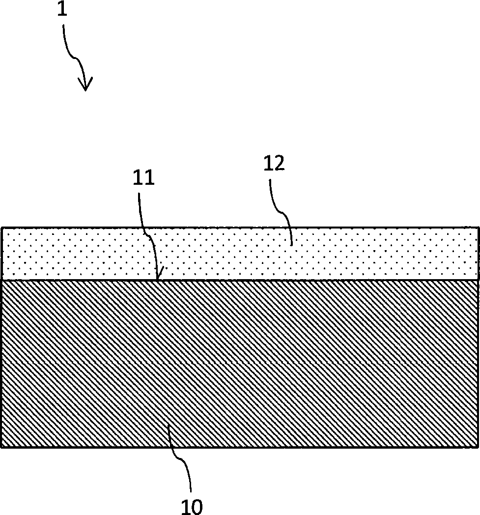
Die in
Etwaige in der Grenzfläche zwischen Substrat
Das Aufbringen einer Druckspannung auf die Oberfläche
Es ist hierbei insbesondere vorgesehen, dass das einkristalline Saphirsubstrat
Das Saphirsubstrat
Unter Annahme temperaturunabhängiger thermischer Ausdehnungskoeffizienten weist Saphir bei Raumtemperatur eine thermische Ausdehnung von 5,0 × 10⁻⁶/K entlang der A-Achse auf, während amorphes Aluminiumoxid einen thermischen Ausdehnungskoeffizienten von 8 × 10⁻⁶/K aufweist.Assuming temperature-independent thermal expansion coefficients, sapphire exhibits a thermal expansion of 5.0 × 10 -6 / K along the A-axis at room temperature, while amorphous alumina has a thermal expansion coefficient of 8 × 10 -6 / K.
Durch den vergleichsweise hohen Anteil von Aluminiumoxid in der aufgebrachten Schicht
Doch nicht nur durch unterschiedliche Ausdehnungskoeffizienten, sondern auch durch das Beschichtungsverfahren selbst können innerhalb der Schicht
Zusätzlich können der Schicht aus optischen Gründen zur Vermeidung von Interferenzerscheinungen aufgrund des unterschiedlichen Brechungsindex von Schicht und Substrat noch eine sogenannte Brechwertanpassschicht zwischen dem Substrat und der verspannenden Aluminiumoxidschicht eingebracht werden. Diese Schicht kann ebenfalls Aluminiumoxid enthalten, wobei der Brechungsindex jener Zwischenschicht zwischen dem Brechungsindex des Saphirsubstrats und dem Brechungsindex der Schicht liegen sollte. Die Dicke jener Zwischenschicht kann typischerweise 60 nm–100 nm, bevorzugt 80 nm betragen.In addition, due to the different refractive index of the layer and the substrate, a so-called refractive index matching layer can be introduced between the substrate and the bracing aluminum oxide layer for optical reasons to avoid interference phenomena. This layer may also contain alumina, wherein the refractive index of that intermediate layer should be between the refractive index of the sapphire substrate and the refractive index of the layer. The thickness of that intermediate layer may typically be 60 nm-100 nm, preferably 80 nm.
BezugszeichenlisteLIST OF REFERENCE NUMBERS
- 11
- Saphirscheibesapphire disk
- 1010
- Saphirsubstratsapphire substrate
- 1111
- Substratoberflächesubstrate surface
- 1212
- Schichtlayer
Claims (8)
Priority Applications (5)
| Application Number | Priority Date | Filing Date | Title |
|---|---|---|---|
| DE102013004558.4A DE102013004558B4 (en) | 2013-03-18 | 2013-03-18 | Method for producing a surface-strained sapphire disk, surface-strained sapphire disk and electrical device with a transparent cover |
| PCT/EP2014/054820 WO2014146948A1 (en) | 2013-03-18 | 2014-03-12 | Surface-tensioned sapphire plate |
| TW103110163A TWI545221B (en) | 2013-03-18 | 2014-03-18 | Surface tensioned sapphire board |
| TW105121441A TWI615278B (en) | 2013-03-18 | 2014-03-18 | Surface tensioned sapphire board |
| US14/453,065 US9617639B2 (en) | 2013-03-18 | 2014-08-06 | Surface-tensioned sapphire plate |
Applications Claiming Priority (1)
| Application Number | Priority Date | Filing Date | Title |
|---|---|---|---|
| DE102013004558.4A DE102013004558B4 (en) | 2013-03-18 | 2013-03-18 | Method for producing a surface-strained sapphire disk, surface-strained sapphire disk and electrical device with a transparent cover |
Publications (2)
| Publication Number | Publication Date |
|---|---|
| DE102013004558A1 DE102013004558A1 (en) | 2014-09-18 |
| DE102013004558B4 true DE102013004558B4 (en) | 2018-04-05 |
Family
ID=50272623
Family Applications (1)
| Application Number | Title | Priority Date | Filing Date |
|---|---|---|---|
| DE102013004558.4A Expired - Fee Related DE102013004558B4 (en) | 2013-03-18 | 2013-03-18 | Method for producing a surface-strained sapphire disk, surface-strained sapphire disk and electrical device with a transparent cover |
Country Status (4)
| Country | Link |
|---|---|
| US (1) | US9617639B2 (en) |
| DE (1) | DE102013004558B4 (en) |
| TW (2) | TWI545221B (en) |
| WO (1) | WO2014146948A1 (en) |
Families Citing this family (4)
| Publication number | Priority date | Publication date | Assignee | Title |
|---|---|---|---|---|
| US9718249B2 (en) | 2012-11-16 | 2017-08-01 | Apple Inc. | Laminated aluminum oxide cover component |
| DE102013004559B4 (en) * | 2013-03-18 | 2015-07-23 | Apple Inc. | Shatter-resistant sapphire disk and method of making the same |
| KR102274075B1 (en) * | 2014-11-27 | 2021-07-08 | 주식회사 아모센스 | Touch Screen Pannel |
| US11269374B2 (en) | 2019-09-11 | 2022-03-08 | Apple Inc. | Electronic device with a cover assembly having an adhesion layer |
Citations (3)
| Publication number | Priority date | Publication date | Assignee | Title |
|---|---|---|---|---|
| DE69612997T2 (en) | 1995-12-04 | 2001-09-20 | Korea Research Institute Of Chemical Technology, Daejeon | METHOD FOR PRODUCING ALUMINUM OXIDE FILMS USING DIALKYL ALUMINUM ALKOXIDE |
| DE112004001032T5 (en) | 2003-06-13 | 2006-05-18 | Han, Joo-Hwan, Kyungsan | Method of Bonding Ceramics: Reaction Diffusion Bonding |
| CN102400213A (en) | 2011-11-18 | 2012-04-04 | 安徽康蓝光电股份有限公司 | Method for epitaxial growth of alumina single crystal film |
Family Cites Families (84)
| Publication number | Priority date | Publication date | Assignee | Title |
|---|---|---|---|---|
| US3713877A (en) * | 1969-02-10 | 1973-01-30 | H Kirchner | Method of strengthening ceramic bodies and strengthened ceramic bodies produced thereby |
| US3736171A (en) | 1969-06-19 | 1973-05-29 | H Kirchner | Method of strengthening ceramics using ion exchange |
| US3809574A (en) * | 1971-07-15 | 1974-05-07 | Rca Corp | Aluminum oxide films for electronic devices |
| US3859714A (en) | 1973-01-12 | 1975-01-14 | Nasa | Bonding of sapphire to sapphire by eutectic mixture of aluminum oxide and zirconium oxide |
| CH613597B (en) | 1975-08-14 | Bbc Brown Boveri & Cie | BEHIND A FRONT GLASS OF A TIMEPIECE, LIQUID CRYSTAL DISPLAY. | |
| US4339300A (en) * | 1977-07-25 | 1982-07-13 | Noble Lowell A | Process for smoothing surfaces of crystalline materials |
| US4675089A (en) | 1985-11-25 | 1987-06-23 | At&T Technologies, Inc. | Low temperature deposition method for high quality aluminum oxide films |
| JPH0266159A (en) | 1988-08-31 | 1990-03-06 | Inax Corp | Formation of aluminum nitride layer |
| US5527596A (en) | 1990-09-27 | 1996-06-18 | Diamonex, Incorporated | Abrasion wear resistant coated substrate product |
| JP3207079B2 (en) | 1995-06-23 | 2001-09-10 | 京セラ株式会社 | Portable communication device |
| US5702654A (en) * | 1996-08-30 | 1997-12-30 | Hughes Electronics | Method of making thermal shock resistant sapphire for IR windows and domes |
| US5935723A (en) | 1997-06-06 | 1999-08-10 | Raytheon Company | Environmentally resistant, infrared-transparent window structure |
| US6012303A (en) | 1997-06-11 | 2000-01-11 | Saphikon, Inc. | Eutectic bonding of single crystal components |
| US5942343A (en) | 1997-10-16 | 1999-08-24 | Raytheon Company | Bonded sapphire, and method of making same |
| FR2787350B1 (en) | 1998-12-21 | 2002-01-04 | Saint Gobain Vitrage | GLASS WITH FUNCTIONAL MESOPOROUS COATING, ESPECIALLY HYDROPHOBIC |
| KR100537685B1 (en) | 1998-12-22 | 2005-12-20 | 가부시키가이샤 쟈판 셀 | Method of joining synthetic corundum and method of manufacturing synthetic corundum cell |
| JP2002008980A (en) | 2000-06-16 | 2002-01-11 | Sony Corp | Semiconductor layer growth method and semiconductor light emitting device manufacturing method |
| US6528123B1 (en) | 2000-06-28 | 2003-03-04 | Sandia Corporation | Coating system to permit direct brazing of ceramics |
| JP3920551B2 (en) | 2000-09-29 | 2007-05-30 | 株式会社山武 | Joining method |
| US7311961B2 (en) | 2000-10-24 | 2007-12-25 | Ppg Industries Ohio, Inc. | Method of making coated articles and coated articles made thereby |
| US20030228476A1 (en) | 2001-10-22 | 2003-12-11 | Harry Buhay | Methods of changing the visible light transmittance of coated articles and coated articles made thereby |
| GB2374235B (en) | 2000-12-29 | 2004-09-22 | Nokia Mobile Phones Ltd | A casing |
| GB2377115B (en) | 2000-12-29 | 2005-06-22 | Nokia Mobile Phones Ltd | A casing for a personal communication device, comprising precious metals, precious stones or ceramics |
| US6649494B2 (en) | 2001-01-29 | 2003-11-18 | Matsushita Electric Industrial Co., Ltd. | Manufacturing method of compound semiconductor wafer |
| WO2002077116A1 (en) | 2001-03-21 | 2002-10-03 | Daikin Industries, Ltd. | Surface-treating agent comprising inorganic/organic composite material |
| US7112359B2 (en) | 2001-08-22 | 2006-09-26 | Inphase Technologies, Inc. | Method and apparatus for multilayer optical articles |
| JP2003063897A (en) | 2001-08-28 | 2003-03-05 | Sony Corp | Nitride III-V compound semiconductor substrate, method of manufacturing the same, method of manufacturing semiconductor light emitting element, and method of manufacturing semiconductor device |
| US7232615B2 (en) | 2001-10-22 | 2007-06-19 | Ppg Industries Ohio, Inc. | Coating stack comprising a layer of barrier coating |
| US6916542B2 (en) | 2001-10-22 | 2005-07-12 | Ppg Industries Ohio, Inc. | Coated articles having a protective coating and cathode targets for making the coated articles |
| WO2003055679A1 (en) | 2001-12-26 | 2003-07-10 | Tdk Corporation | Article having composite hard coat layer and method for forming composite hard coat layer |
| AU2003225135A1 (en) | 2002-04-25 | 2003-11-11 | Ppg Industries Ohio, Inc. | Method of making coated articles having an oxygen barrier coating and coated articles made thereby |
| US8021758B2 (en) | 2002-12-23 | 2011-09-20 | Applied Thin Films, Inc. | Aluminum phosphate compounds, coatings, related composites and applications |
| EP1655766B1 (en) * | 2003-08-12 | 2014-04-30 | Nippon Telegraph And Telephone Corporation | Substrate for growth of nitride semiconductor |
| JP2006276617A (en) * | 2005-03-30 | 2006-10-12 | Sumitomo Chemical Co Ltd | Polarization conversion element and projection type liquid crystal display device using the same |
| TWM278556U (en) | 2005-05-19 | 2005-10-21 | Lutek Ind Co Ltd | Nano-meter protecting film structure for source material |
| US7584689B2 (en) | 2005-06-10 | 2009-09-08 | Saint-Gobain Ceramics & Plastics, Inc. | Transparent ceramic composite armor |
| US7592629B2 (en) | 2005-07-18 | 2009-09-22 | Samsung Corning Co., Ltd. | Gallium nitride thin film on sapphire substrate having reduced bending deformation |
| US7803451B2 (en) | 2005-07-29 | 2010-09-28 | Onyx Optics, Inc. | Optical composites between similar and between dissimilar materials |
| US20070048526A1 (en) | 2005-08-31 | 2007-03-01 | Hoffman William F Iii | Recycling compatible hard coating |
| FR2895275B1 (en) | 2005-12-22 | 2008-07-25 | Framatome Sa | GAS SEPARATION MEMBRANES CONTAINING SILICA MICROPOROUS SILICA LAYER DOPED BY TRIVALENT ELEMENT |
| KR20070070516A (en) | 2005-12-29 | 2007-07-04 | 삼성전자주식회사 | Display panel and manufacturing method thereof |
| RU2436875C2 (en) | 2006-09-22 | 2011-12-20 | Сэнт-Гобэн Керамикс Энд Пластикс, Инк. | Method and apparatus for growing sapphire monocrystal with orientation in c-plane |
| JP5090710B2 (en) | 2006-10-30 | 2012-12-05 | 京セラ株式会社 | Portable electronic devices |
| US20080139885A1 (en) | 2006-11-16 | 2008-06-12 | Jamie Knapp | Autoclavable antireflective coatings for endoscopy windows and related methods |
| US8031174B2 (en) | 2007-01-03 | 2011-10-04 | Apple Inc. | Multi-touch surface stackup arrangement |
| DE102008002024A1 (en) | 2007-06-05 | 2008-12-11 | Carl Zeiss Smt Ag | Optical element, projection lens and projection exposure machine with it |
| US8728634B2 (en) | 2007-06-13 | 2014-05-20 | Ppg Industries Ohio, Inc. | Appliance transparency |
| US8015970B2 (en) | 2007-07-26 | 2011-09-13 | 3M Innovative Properties Company | Respirator, welding helmet, or face shield that has low surface energy hard-coat lens |
| US7966785B2 (en) | 2007-08-22 | 2011-06-28 | Apple Inc. | Laminated display window and device incorporating same |
| US20090263651A1 (en) | 2008-02-06 | 2009-10-22 | Cook Richard L | Optically transparent resilient laminate materials and methods of manufacture |
| JP2009204404A (en) | 2008-02-27 | 2009-09-10 | Seiko Epson Corp | Timepiece, light-transmitting member, and its manufacturing method |
| US8055003B2 (en) | 2008-04-01 | 2011-11-08 | Apple Inc. | Acoustic systems for electronic devices |
| US8491718B2 (en) | 2008-05-28 | 2013-07-23 | Karin Chaudhari | Methods of growing heteroepitaxial single crystal or large grained semiconductor films and devices thereon |
| TW200948734A (en) | 2008-05-30 | 2009-12-01 | Corning Inc | Damage resistant glass article for use as a cover plate in electronic devices |
| JP5326407B2 (en) | 2008-07-31 | 2013-10-30 | セイコーエプソン株式会社 | Watch cover glass and watch |
| FR2934854B1 (en) | 2008-08-08 | 2011-04-22 | Beatrice Drazenovic | SEMICONDUCTOR CERAMIC |
| US20100124642A1 (en) | 2008-11-19 | 2010-05-20 | Ppg Industries Ohio, Inc. | Undercoating layers providing improved conductive topcoat functionality |
| US8133599B2 (en) | 2008-11-19 | 2012-03-13 | Ppg Industries Ohio, Inc | Undercoating layers providing improved photoactive topcoat functionality |
| US7998586B2 (en) | 2008-11-19 | 2011-08-16 | Ppg Industries Ohio, Inc. | Undercoating layers providing improved topcoat functionality |
| US8492292B2 (en) | 2009-06-29 | 2013-07-23 | Applied Materials, Inc. | Methods of forming oxide layers on substrates |
| DE102009034532A1 (en) | 2009-07-23 | 2011-02-03 | Msg Lithoglas Ag | Process for producing a structured coating on a substrate, coated substrate and semifinished product with a coated substrate |
| WO2011050170A2 (en) | 2009-10-22 | 2011-04-28 | Advanced Renewable Energy Company Llc | Crystal growth methods and systems |
| CN102111972B (en) | 2009-12-29 | 2015-07-29 | 深圳富泰宏精密工业有限公司 | Case of electronic device |
| JP2011201759A (en) * | 2010-03-05 | 2011-10-13 | Namiki Precision Jewel Co Ltd | Single crystal substrate with multilayer film, production method for single crystal substrate with multilayer film, and device production method |
| US9956743B2 (en) | 2010-12-20 | 2018-05-01 | The Regents Of The University Of California | Superhydrophobic and superoleophobic nanosurfaces |
| GB201102724D0 (en) | 2011-02-17 | 2011-03-30 | Pilkington Group Ltd | Heat treatable coated glass pane |
| GB201106788D0 (en) | 2011-04-21 | 2011-06-01 | Pilkington Group Ltd | Heat treatable coated glass pane |
| US8968058B2 (en) | 2011-05-05 | 2015-03-03 | Nexplanar Corporation | Polishing pad with alignment feature |
| TWM438642U (en) | 2011-12-27 | 2012-10-01 | Tera Xtal Technology Corp | Apparatus for capturing image and LEN device |
| US20150044447A1 (en) | 2012-02-13 | 2015-02-12 | Silicon Genesis Corporation | Cleaving thin layer from bulk material and apparatus including cleaved thin layer |
| US10052848B2 (en) | 2012-03-06 | 2018-08-21 | Apple Inc. | Sapphire laminates |
| WO2013134159A2 (en) | 2012-03-06 | 2013-09-12 | Apple Inc. | Sapphire laminates |
| US9578769B2 (en) | 2012-05-29 | 2017-02-21 | Apple Inc. | Components of an electronic device and methods for their assembly |
| CN102723265B (en) | 2012-06-18 | 2014-12-24 | 苏州阿特斯阳光电力科技有限公司 | Aluminum doping method for silicon wafer |
| CN103814160B (en) | 2012-08-30 | 2018-09-14 | 日本碍子株式会社 | Composite substrate, method for producing same, method for producing functional layer composed of nitride of group 13 elements, and functional element |
| WO2014047479A1 (en) * | 2012-09-21 | 2014-03-27 | Apple Inc. | Oleophobic coating on sapphire |
| JP6028495B2 (en) | 2012-09-27 | 2016-11-16 | Toto株式会社 | Photocatalyst member |
| KR102281607B1 (en) | 2012-11-14 | 2021-07-26 | 지티에이티 코포레이션 | A mobile electronic device comprising an ultrathin sapphire cover plate |
| US9718249B2 (en) * | 2012-11-16 | 2017-08-01 | Apple Inc. | Laminated aluminum oxide cover component |
| US9377912B2 (en) | 2012-12-11 | 2016-06-28 | Gtat Corporation | Mobile electronic device comprising a modified sapphire |
| US9623628B2 (en) | 2013-01-10 | 2017-04-18 | Apple Inc. | Sapphire component with residual compressive stress |
| WO2014126777A1 (en) * | 2013-02-15 | 2014-08-21 | Gt Crystal Systems, Llc | A mobile electronic device comprising a multilayer sapphire cover plate having layers with different orientations |
| EP2778252A3 (en) | 2013-03-15 | 2014-12-10 | Apple Inc. | Layered Coatings For Sapphire Structure |
| WO2014193823A1 (en) | 2013-05-28 | 2014-12-04 | Gtat Corporation | A mobile electronic device cover plate comprising a thin sapphire layer |
-
2013
- 2013-03-18 DE DE102013004558.4A patent/DE102013004558B4/en not_active Expired - Fee Related
-
2014
- 2014-03-12 WO PCT/EP2014/054820 patent/WO2014146948A1/en not_active Ceased
- 2014-03-18 TW TW103110163A patent/TWI545221B/en not_active IP Right Cessation
- 2014-03-18 TW TW105121441A patent/TWI615278B/en not_active IP Right Cessation
- 2014-08-06 US US14/453,065 patent/US9617639B2/en active Active
Patent Citations (3)
| Publication number | Priority date | Publication date | Assignee | Title |
|---|---|---|---|---|
| DE69612997T2 (en) | 1995-12-04 | 2001-09-20 | Korea Research Institute Of Chemical Technology, Daejeon | METHOD FOR PRODUCING ALUMINUM OXIDE FILMS USING DIALKYL ALUMINUM ALKOXIDE |
| DE112004001032T5 (en) | 2003-06-13 | 2006-05-18 | Han, Joo-Hwan, Kyungsan | Method of Bonding Ceramics: Reaction Diffusion Bonding |
| CN102400213A (en) | 2011-11-18 | 2012-04-04 | 安徽康蓝光电股份有限公司 | Method for epitaxial growth of alumina single crystal film |
Non-Patent Citations (1)
| Title |
|---|
| Google-Übersetzung der CN 102400213A |
Also Published As
| Publication number | Publication date |
|---|---|
| WO2014146948A1 (en) | 2014-09-25 |
| TW201636206A (en) | 2016-10-16 |
| TW201506188A (en) | 2015-02-16 |
| DE102013004558A1 (en) | 2014-09-18 |
| US20140349092A1 (en) | 2014-11-27 |
| US9617639B2 (en) | 2017-04-11 |
| TWI615278B (en) | 2018-02-21 |
| TWI545221B (en) | 2016-08-11 |
Similar Documents
| Publication | Publication Date | Title |
|---|---|---|
| DE102013004559B4 (en) | Shatter-resistant sapphire disk and method of making the same | |
| DE102014104799B4 (en) | Substrate with a coating to increase scratch resistance, process for its production and its use | |
| DE102013004558B4 (en) | Method for producing a surface-strained sapphire disk, surface-strained sapphire disk and electrical device with a transparent cover | |
| DE102015106368B4 (en) | A coated article and method of making a coated article | |
| DE102007033338A1 (en) | Hard material-coated glass or glass-ceramic article and method for its production | |
| DE112010002790T5 (en) | METHOD OF MANUFACTURING A PIEZOELECTRIC LAYER AND PIEZOELECTRIC LAYER PRODUCED BY THE MANUFACTURING METHOD | |
| DE112011101379T5 (en) | Coating for cutting tools | |
| DE102014205867A1 (en) | Transparent ceramic with functional coating | |
| DE4220717A1 (en) | METHOD FOR FORMING A SILICON CARBIDE FILM | |
| DE102014105939A1 (en) | Process for producing an anti-reflection coating on a silicone surface and optical element | |
| DE102004019575A1 (en) | Method for producing transmission-improving and / or reflection-reducing optical layers | |
| WO2008017723A1 (en) | Temperable solar control layer system and method for the production thereof | |
| DE102014108060A1 (en) | Glass element with a chemically tempered substrate and a compensation layer and method for its production | |
| DE102016100914B4 (en) | Method for producing a porous refractive index gradient layer | |
| DE19528329A1 (en) | X-ray transparent layer material, process for its production and its use | |
| DE10250564B4 (en) | Process for coating a surface, product and use of the product | |
| DE102008028540A1 (en) | Depositing gradient layer on plastics substrate, e.g. scratch-resistant layer on lens, uses magnetron plasma enhanced chemical vapor deposition to give increasing organic compound content | |
| DE102012200799A1 (en) | Fire protection element with protective coating and its manufacturing process | |
| DE102015200692A1 (en) | Epitaxial diamond layer and process for its preparation | |
| DE102010055659A1 (en) | Method for depositing dielectric layers in vacuum and use of the method | |
| EP2699705A1 (en) | Method for depositing a transparent barrier layer system | |
| DE102016210811A1 (en) | Transparent ceramic as a component for break-proof optics | |
| DE102023133273A1 (en) | watch glass | |
| DE102023133275A1 (en) | Process for producing a transparent, scratch-resistant component | |
| Fan et al. | The effect of copper substrate’s roughness on graphene growth process via PECVD |
Legal Events
| Date | Code | Title | Description |
|---|---|---|---|
| R012 | Request for examination validly filed | ||
| R082 | Change of representative |
Representative=s name: BARDEHLE PAGENBERG PARTNERSCHAFT MBB PATENTANW, DE |
|
| R016 | Response to examination communication | ||
| R016 | Response to examination communication | ||
| R016 | Response to examination communication | ||
| R018 | Grant decision by examination section/examining division | ||
| R020 | Patent grant now final | ||
| R119 | Application deemed withdrawn, or ip right lapsed, due to non-payment of renewal fee |