DE102010054893A1 - Radiation-emitting organic-electronic device and method for its production - Google Patents
Radiation-emitting organic-electronic device and method for its production Download PDFInfo
- Publication number
- DE102010054893A1 DE102010054893A1 DE102010054893A DE102010054893A DE102010054893A1 DE 102010054893 A1 DE102010054893 A1 DE 102010054893A1 DE 102010054893 A DE102010054893 A DE 102010054893A DE 102010054893 A DE102010054893 A DE 102010054893A DE 102010054893 A1 DE102010054893 A1 DE 102010054893A1
- Authority
- DE
- Germany
- Prior art keywords
- emitter
- layer
- matrix material
- radiation
- bis
- Prior art date
- Legal status (The legal status is an assumption and is not a legal conclusion. Google has not performed a legal analysis and makes no representation as to the accuracy of the status listed.)
- Withdrawn
Links
Images


Classifications
-
- H—ELECTRICITY
- H10—SEMICONDUCTOR DEVICES; ELECTRIC SOLID-STATE DEVICES NOT OTHERWISE PROVIDED FOR
- H10K—ORGANIC ELECTRIC SOLID-STATE DEVICES
- H10K71/00—Manufacture or treatment specially adapted for the organic devices covered by this subclass
- H10K71/10—Deposition of organic active material
- H10K71/191—Deposition of organic active material characterised by provisions for the orientation or alignment of the layer to be deposited
-
- H—ELECTRICITY
- H10—SEMICONDUCTOR DEVICES; ELECTRIC SOLID-STATE DEVICES NOT OTHERWISE PROVIDED FOR
- H10K—ORGANIC ELECTRIC SOLID-STATE DEVICES
- H10K50/00—Organic light-emitting devices
- H10K50/10—OLEDs or polymer light-emitting diodes [PLED]
- H10K50/11—OLEDs or polymer light-emitting diodes [PLED] characterised by the electroluminescent [EL] layers
-
- H—ELECTRICITY
- H10—SEMICONDUCTOR DEVICES; ELECTRIC SOLID-STATE DEVICES NOT OTHERWISE PROVIDED FOR
- H10K—ORGANIC ELECTRIC SOLID-STATE DEVICES
- H10K50/00—Organic light-emitting devices
- H10K50/80—Constructional details
- H10K50/868—Arrangements for polarized light emission
-
- H—ELECTRICITY
- H10—SEMICONDUCTOR DEVICES; ELECTRIC SOLID-STATE DEVICES NOT OTHERWISE PROVIDED FOR
- H10K—ORGANIC ELECTRIC SOLID-STATE DEVICES
- H10K71/00—Manufacture or treatment specially adapted for the organic devices covered by this subclass
-
- H—ELECTRICITY
- H10—SEMICONDUCTOR DEVICES; ELECTRIC SOLID-STATE DEVICES NOT OTHERWISE PROVIDED FOR
- H10K—ORGANIC ELECTRIC SOLID-STATE DEVICES
- H10K71/00—Manufacture or treatment specially adapted for the organic devices covered by this subclass
- H10K71/10—Deposition of organic active material
- H10K71/16—Deposition of organic active material using physical vapour deposition [PVD], e.g. vacuum deposition or sputtering
- H10K71/164—Deposition of organic active material using physical vapour deposition [PVD], e.g. vacuum deposition or sputtering using vacuum deposition
-
- H—ELECTRICITY
- H10—SEMICONDUCTOR DEVICES; ELECTRIC SOLID-STATE DEVICES NOT OTHERWISE PROVIDED FOR
- H10K—ORGANIC ELECTRIC SOLID-STATE DEVICES
- H10K85/00—Organic materials used in the body or electrodes of devices covered by this subclass
- H10K85/30—Coordination compounds
- H10K85/331—Metal complexes comprising an iron-series metal, e.g. Fe, Co, Ni
-
- H—ELECTRICITY
- H10—SEMICONDUCTOR DEVICES; ELECTRIC SOLID-STATE DEVICES NOT OTHERWISE PROVIDED FOR
- H10K—ORGANIC ELECTRIC SOLID-STATE DEVICES
- H10K85/00—Organic materials used in the body or electrodes of devices covered by this subclass
- H10K85/30—Coordination compounds
- H10K85/341—Transition metal complexes, e.g. Ru(II)polypyridine complexes
- H10K85/342—Transition metal complexes, e.g. Ru(II)polypyridine complexes comprising iridium
-
- H—ELECTRICITY
- H10—SEMICONDUCTOR DEVICES; ELECTRIC SOLID-STATE DEVICES NOT OTHERWISE PROVIDED FOR
- H10K—ORGANIC ELECTRIC SOLID-STATE DEVICES
- H10K85/00—Organic materials used in the body or electrodes of devices covered by this subclass
- H10K85/30—Coordination compounds
- H10K85/341—Transition metal complexes, e.g. Ru(II)polypyridine complexes
- H10K85/346—Transition metal complexes, e.g. Ru(II)polypyridine complexes comprising platinum
-
- H—ELECTRICITY
- H10—SEMICONDUCTOR DEVICES; ELECTRIC SOLID-STATE DEVICES NOT OTHERWISE PROVIDED FOR
- H10K—ORGANIC ELECTRIC SOLID-STATE DEVICES
- H10K2101/00—Properties of the organic materials covered by group H10K85/00
- H10K2101/10—Triplet emission
-
- H—ELECTRICITY
- H10—SEMICONDUCTOR DEVICES; ELECTRIC SOLID-STATE DEVICES NOT OTHERWISE PROVIDED FOR
- H10K—ORGANIC ELECTRIC SOLID-STATE DEVICES
- H10K71/00—Manufacture or treatment specially adapted for the organic devices covered by this subclass
- H10K71/40—Thermal treatment, e.g. annealing in the presence of a solvent vapour
-
- H—ELECTRICITY
- H10—SEMICONDUCTOR DEVICES; ELECTRIC SOLID-STATE DEVICES NOT OTHERWISE PROVIDED FOR
- H10K—ORGANIC ELECTRIC SOLID-STATE DEVICES
- H10K71/00—Manufacture or treatment specially adapted for the organic devices covered by this subclass
- H10K71/851—Division of substrate
Landscapes
- Chemical & Material Sciences (AREA)
- Engineering & Computer Science (AREA)
- Manufacturing & Machinery (AREA)
- Inorganic Chemistry (AREA)
- Materials Engineering (AREA)
- Physics & Mathematics (AREA)
- Optics & Photonics (AREA)
- Crystallography & Structural Chemistry (AREA)
- Electroluminescent Light Sources (AREA)
Abstract
Es wird ein Verfahren zur Herstellung eines einer strahlungsemittierenden organisch elektronischen Vorrichtung mit einer ersten und einer zweiten Elektrodenschicht und einer Emitterschicht mit folgenden Schritten angegeben und eine damit hergestellte Vorrichtung: A) Bereitstellen eines phosphoreszenten Emitters mit anisotroper Molekülstruktur und eines Matrixmaterials, B) Aufbringen der ersten Elektrodenschicht auf ein Substrat, C) Aufbringen der Emitterschicht unter thermodynamischer Kontrolle, wobei der phosphoreszente Emitter und das Matrixmaterial im Vakuum verdampft werden und auf der ersten Elektrodenschicht abgeschieden werden, so dass eine anisotrope Ausrichtung der Moleküle des phosphoreszenten Emitters erfolgt, D) Aufbringen der zweiten Elektrodenschicht auf der Emitterschicht.A method for producing a radiation-emitting organic electronic device with a first and a second electrode layer and an emitter layer with the following steps is specified and a device produced therewith: A) providing a phosphorescent emitter with an anisotropic molecular structure and a matrix material, B) applying the first Electrode layer on a substrate, C) application of the emitter layer under thermodynamic control, the phosphorescent emitter and the matrix material being evaporated in vacuo and deposited on the first electrode layer so that the molecules of the phosphorescent emitter are anisotropically aligned, D) application of the second Electrode layer on the emitter layer.
Description
Die vorliegende Erfindung betrifft ein Verfahren zur Herstellung einer strahlungsemittierenden organisch-elektronischen Vorrichtung mit gegenüber dem Stand der Technik verbesserter Effizienz, bei dem aus Materialien mit anisotroper Molekülstruktur unter thermodynamischer Kontrolle eine Emitterschicht der organisch-elektronischen Vorrichtung gebildet wird. Die vorliegende Erfindung betrifft ferner eine strahlungsemittierende organisch-elektronische Vorrichtung, die mit diesem Verfahren herstellbar ist.The present invention relates to a method for producing a radiation-emitting organic-electronic device with improved efficiency compared with the prior art, in which an emitter layer of the organic-electronic device is formed from materials with anisotropic molecular structure under thermodynamic control. The present invention further relates to a radiation-emitting organic-electronic device that can be produced by this method.
In strahlungsemittierenden organisch-elektronischen Vorrichtungen, insbesondere in organischen Leuchtdioden (OLEDs) wird die generierte Strahlung nur zum Teil direkt ausgekoppelt. Folgende Verlustkanäle wurden beobachtet: wellenleitende Effekte des transparenten Substrats (das im Strahlengang der emittierten Strahlung angeordnet ist), wellenleitende Effekte in den organischen Schichten und der transparenten Elektrode (die im Strahlengang der emittierten Strahlung angeordnet ist), Absorptionsverluste (aufgrund der Materialien, durch die emittierte Strahlung hindurchtritt) und die Ausbildung von Oberflächenplasmonen, insbesondere an einer metallischen Elektrode (beispielsweise der Kathode).In radiation-emitting organic-electronic devices, in particular in organic light-emitting diodes (OLEDs), the generated radiation is only partially decoupled directly. The following loss channels have been observed: waveguiding effects of the transparent substrate (located in the beam path of the emitted radiation), waveguiding effects in the organic layers and the transparent electrode (located in the beam path of the emitted radiation), absorption losses (due to the materials through which emitted radiation passes) and the formation of surface plasmons, in particular on a metallic electrode (for example, the cathode).
Es ist eine Aufgabe der vorliegenden Erfindung, ein Verfahren und eine damit hergestellte strahlungsemittierende organisch-elektronische Vorrichtung anzugeben, bei der die Effizienz gegenüber dem Stand der Technik verbessert ist und insbesondere die Verluste durch zumindest einen der genannten Verlustkanäle vermindert sind.It is an object of the present invention to provide a method and a radiation-emitting organic-electronic device produced therewith, in which the efficiency is improved over the prior art and in particular the losses are reduced by at least one of said loss channels.
Diese Aufgabe wird durch das Verfahren zur Herstellung einer strahlungsemittierenden organisch-elektronischen Vorrichtung und die Vorrichtung selbst gemäß den unabhängigen Ansprüchen gelöst. Unteransprüche, die Beschreibung und die Zeichnungen lehren vorteilhafte Ausführungsformen und Weiterbildungen hiervon.This object is achieved by the method for producing a radiation-emitting organic-electronic device and the device itself according to the independent claims. Subclaims, the description and the drawings teach advantageous embodiments and developments thereof.
Gemäß einer Ausführungsform umfasst das Verfahren zur Herstellung einer strahlungsemittierenden organisch-elektronischen Vorrichtung die folgenden Schritte:
- A) ein phosphoreszenter Emitter mit einer anisotropen Molekülstruktur und ein Matrixmaterial werden bereitgestellt;
- B) eine erste Elektrodenschicht wird auf ein Substrat aufgebracht;
- C) auf der ersten Elektrodenschicht wird eine Emitterschicht unter thermodynamischer Kontrolle aufgebracht, wobei der phosphoreszente Emitter und das Matrixmaterial im Vakuum verdampft werden und auf der Elektrodenschicht abgeschieden werden; hierbei erfolgt durch die thermodynamische Kontrolle eine anisotrope Ausrichtung der Moleküle des phosphoreszenten Emitters;
- D) eine zweite Elektrodenschicht wird auf der Emitterschicht aufgebracht.
- A) a phosphorescent emitter having an anisotropic molecular structure and a matrix material are provided;
- B) a first electrode layer is applied to a substrate;
- C) on the first electrode layer, an emitter layer is applied under thermodynamic control, wherein the phosphorescent emitter and the matrix material are evaporated in vacuum and deposited on the electrode layer; In this case, the thermodynamic control is an anisotropic alignment of the molecules of the phosphorescent emitter;
- D) a second electrode layer is applied to the emitter layer.
Unter einer anisotropen Molekülstruktur wird im Rahmen der vorliegenden Anmeldung verstanden, dass die eingesetzten Moleküle keine im Wesentlichen kugelige Molekülstruktur ausbilden, sondern eine eher langgestreckte Molekülstruktur. Um dies zu erreichen, weisen die phosphoreszenten Emitter insbesondere zumindest zweierlei unterschiedliche Liganden auf (insbesondere Liganden die sich hinsichtlich ihrer an das Zentralatom koordinierenden Atome unterscheiden) oder weisen eine quadratisch-planare Umgebung des Zentralatoms auf.In the context of the present application, an anisotropic molecular structure is understood to mean that the molecules used do not form a substantially spherical molecular structure, but rather a rather elongated molecular structure. In order to achieve this, the phosphorescent emitters in particular have at least two different different ligands (in particular ligands which differ with respect to their atoms coordinating with the central atom) or have a square-planar environment of the central atom.
Im Rahmen der vorliegenden Erfindung kann eine erste Schicht, die „auf” einer zweiten Schicht angeordnet oder aufgebracht ist, bedeuten, dass die erste Schicht unmittelbar in direktem mechanischen und/oder elektrischen Kontakt auf der zweiten Schicht angeordnet oder aufgebracht ist. Weiterhin kann auch ein mittelbarer Kontakt bezeichnet sein, bei dem weitere Schichten zwischen der ersten Schicht und der zweiten Schicht angeordnet sind.In the context of the present invention, a first layer which is arranged or applied "on" a second layer may mean that the first layer is arranged or applied directly in direct mechanical and / or electrical contact with the second layer. Furthermore, an indirect contact may also be designated, in which further layers are arranged between the first layer and the second layer.
Unter einem Aufbringen unter thermodynamischer Kontrolle wird anmeldungsgemäß verstanden, dass bei der Abscheidung der Emittermoleküle und der Moleküle des Matrixmaterials keine willkürliche Ausrichtung der abgeschiedenen Moleküle erfolgt, sondern dass vielmehr die Ausrichtung zumindest teilweise in einer Vorzugsrichtung stattfindet. Damit geht einher, dass auch die Übergangsdipolmomente der Emittermoleküle in der Summe eine anisotrope Verteilung innerhalb der Matrix aufweisen, die insbesondere dadurch charakterisiert ist, dass mehr Übergangsdipolmomente parallel zur Schichtebene der Emitterschicht ausgerichtet sind als Übergangsdipolmomente, die orthogonal hierzu ausgerichtet sind. Die Übergangsdipolmomente weisen eine bestimmte Orientierung im emittierenden Molekül auf und sind deshalb relevant, weil der Emissionsprozess ein Dipol-Übergang ist. Die thermodynamische Kontrolle erfordert also, dass anders als bei der kinetischen Kontrolle ein Emittermolekül nicht automatisch in der Position ”eingefroren” wird, in der es erstmalig mit der Oberfläche, auf der es abgeschieden wird, in Wechselwirkung tritt, sondern dass vielmehr während der Abscheidung oder in einem späteren Schritt eine Umorientierung erfolgen kann, bei der eine Ausrichtung benachbarter Moleküle erfolgt, wobei eine thermodynamisch günstigere Konfiguration eingenommen werden kann. Eine derartige anisotrope Ausrichtung der Emittermoleküle ist insbesondere dann möglich, wenn sowohl für den Emitter als auch für das Matrixmaterial Ausgangsmaterialien ausgewählt werden, die eine anisotrope Molekülstruktur besitzen.An application under thermodynamic control according to the application is understood to mean that during the deposition of the emitter molecules and the molecules of the matrix material no arbitrary alignment of the deposited molecules takes place, but rather that the alignment takes place at least partially in a preferred direction. This is accompanied by the fact that the transition dipole moments of the emitter molecules as a whole also have an anisotropic distribution within the matrix, which is characterized in particular by the fact that more transition dipole moments are aligned parallel to the layer plane of the emitter layer than transition dipole moments aligned orthogonally to it. The transition dipole moments have a certain orientation in the emitting molecule and are relevant because the emission process is a dipole transition. The thermodynamic control thus requires that unlike kinetic control, an emitter molecule is not automatically "frozen" in the position in which it initially interacts with the surface on which it is deposited, but rather during deposition or In a later step, a reorientation can take place in which an alignment of adjacent molecules takes place, wherein a thermodynamically more favorable configuration can be assumed. Such anisotropic alignment of the emitter molecules is possible in particular when starting materials are selected which possess an anisotropic molecular structure both for the emitter and for the matrix material.
Erfindungsgemäß wurde also erkannt, dass durch die Ausgangsmaterialien mit anisotroper Molekülstruktur Emitterschichten erzeugt werden können, in denen die einzelnen Emittermoleküle und damit auch die Übergangsdipolmomente der emittierenden Moleküle eine Vorzugsausrichtung aufweisen. Im Idealfall liegen die Emittermoleküle im Wesentlichen parallel ausgerichtet vor, wobei dann beobachtet wird, dass fast kein Verlust durch Plasmonen auftritt. Der Verlustkanal ”Effizientverlust durch Plasmonenauskopplung” wird somit teilweise versperrt, sodass letztlich die Gesamteffizienz deutlich steigt. Durch die im Wesentlichen vorhandene Vorzugsausrichtung der Emittermoleküle, die vorzugsweise parallel zur Substratoberfläche ausgerichtet sind, kann nur in beschränktem Umfang eine Wechselwirkung des bei der Rekombination von Elektron und Loch entstehenden elektromagnetischen Felds mit den Plasmonen der Metallschicht erfolgen. According to the invention, it has thus been recognized that emitter layers can be produced by the starting materials with anisotropic molecular structure in which the individual emitter molecules and thus also the transition dipole moments of the emitting molecules have a preferred orientation. Ideally, the emitter molecules are substantially aligned in parallel, and it is then observed that there is almost no loss by plasmons. The loss channel "Efficiency loss by plasmon decoupling" is thus partially blocked, so that ultimately the overall efficiency increases significantly. Due to the essentially existing preferred orientation of the emitter molecules, which are preferably aligned parallel to the substrate surface, an interaction of the electromagnetic field resulting from the recombination of the electron and the hole with the plasmon of the metal layer can only take place to a limited extent.
Unter einem Plasmon wird eine Ladungsträgerdichteschwingung in der Metallschicht der ersten Elektrode verstanden. Insbesondere. kann ein von einem rekombinierenden Exziton erzeugtes elektromagnetisches Feld freie Ladungsträger, insbesondere Elektronen, in der Metallschicht einer Elektrode zu Ladungsträgerdichteschwingungen anregen. Mit anderen Worten kann das bei der Rekombination eines Exzitons entstehende elektromagnetische Feld an ein Plasmon in der Metallschicht der Elektrode koppeln, sodass die Rekombinationsenergie zumindest teilweise auf das Plasmon übergehen kann.A plasmon is understood to mean a charge carrier density oscillation in the metal layer of the first electrode. Especially. For example, an electromagnetic field generated by a recombinant exciton can excite free charge carriers, in particular electrons, in the metal layer of an electrode to charge carrier density oscillations. In other words, the electromagnetic field resulting from the recombination of an exciton can couple to a plasmon in the metal layer of the electrode so that the recombination energy can at least partially pass to the plasmon.
Insbesondere bezeichnen Plasmonen (präziser: Oberflächenplasmonen) hierbei longitudinale Ladungsträgerdichteschwingungen, die parallel zur Erstreckungsebene einer Oberfläche der Metallschicht einer Elektrode an dieser Oberfläche auftreten. Oberflächenplasmonen können dabei insbesondere an der der Emitterschicht zugewandten Oberfläche der Metallschicht dieser Elektrode erzeugt werden.In particular, plasmas (more precisely: surface plasmons) designate longitudinal charge carrier density oscillations which occur parallel to the plane of extension of a surface of the metal layer of an electrode on this surface. Surface plasmons can be produced in particular on the surface of the metal layer of this electrode facing the emitter layer.
Gemäß einer Ausführungsform des anmeldungsgemäßen Verfahrens erfolgt die thermodynamische Kontrolle in Schritt C), indem eine Aufwachsrate gewählt wird, die kleiner oder gleich als 0,5 nm/s ist. Insbesondere kann die Aufwachsrate kleiner als 0,2 nm/s sein und ist häufig auch kleiner als 0,1 nm/s. Oft ist die Aufwachsrate kleiner als 0,05 nm/s; sie kann beispielsweise auch kleiner als 0,025 nm/s sein. Bei einer Aufwachsrate von 0,05 nm/s beträgt die Abscheidungszeit für eine 10 nm dicke Emitterschicht dann etwa 200 s. Unter der Aufwachsrate ist dabei die Geschwindigkeit zu verstehen, mit der in Schritt C) auf der ersten Elektrodenschicht die Emitterschicht abgeschieden wird. Im Regelfall ist die dabei abgeschiedene Stoffmenge beispielsweise im Wesentlichen identisch mit der aus einer Vorlage verdampften Stoffmenge. Eine besonders langsame Aufwachsrate kann beispielsweise dann gewählt werden, wenn die Materialien für die Emitterschicht keine erhöhte Temperatur des zu beschichtenden Substrats zulassen (vergleiche nachfolgende Ausführungsform).According to one embodiment of the method according to the application, the thermodynamic control is carried out in step C) by selecting a growth rate which is less than or equal to 0.5 nm / s. In particular, the growth rate may be less than 0.2 nm / s and is often less than 0.1 nm / s. Often the growth rate is less than 0.05 nm / s; for example, it may also be less than 0.025 nm / s. At a growth rate of 0.05 nm / s, the deposition time for a 10 nm thick emitter layer is then about 200 s. The growth rate is to be understood as the rate at which the emitter layer is deposited on the first electrode layer in step C). As a rule, the amount of substance deposited in this case is essentially identical to the amount of substance evaporated from a receiver, for example. A particularly slow growth rate can be selected, for example, if the materials for the emitter layer do not allow an increased temperature of the substrate to be coated (compare the following embodiment).
Gemäß einer weiteren Ausführungsform wird die thermodynamische Kontrolle in Schritt C) dadurch erreicht, dass nach und/oder während dem Abscheidungsschritt (Schritt C)) die abgeschiedene Schicht (insbesondere vor dem Abscheiden weiterer Schichten) einer Temperaturbehandlung unterworfen wird. Die Emitterschicht wird insbesondere auf eine gegenüber Raumtemperatur erhöhte Temperatur gebracht oder auf einer derartigen Temperatur gehalten. Auf die abgeschiedene Schicht können also entweder während der Abscheidung erhöhte Temperaturen einwirken und/oder nach vollständiger Abscheidung der Emitterschicht (und vor Abscheiden einer weiteren Schicht) kann ein Tempern der abgeschiedenen Schicht erfolgen. Bei einer derartigen Temperaturbehandlung wird die Schicht also in einen Zustand gebracht, bei dem eine Umorientierung, insbesondere der Emittermoleküle, möglich ist, sodass eine Ausrichtung der Emittermoleküle erfolgen kann. Dieser ausgerichtete Zustand kann dann durch die Abkühlung nachfolgend eingefroren werden. Die Temperaturbehandlung kann hierbei insbesondere erfolgen, indem die Emitterschicht beziehungsweise die substratseitig angrenzende Schicht (beispielsweise über ein beheiztes Substrat) erwärmt wird. Die Emitterschicht kann dabei beispielsweise auf eine Temperatur zwischen 30°C und 100°C gebracht werden. Wesentlich hierbei ist, dass die gewählten Temperaturen keine Beschädigung der aufzubringenden oder der bereits aufgebrachten Schichten der organisch-elektronischen Vorrichtung hervorrufen.According to a further embodiment, the thermodynamic control in step C) is achieved by subjecting the deposited layer (in particular before depositing further layers) to a temperature treatment after and / or during the deposition step (step C)). In particular, the emitter layer is brought to a temperature which is elevated in relation to room temperature or kept at such a temperature. The deposited layer can therefore either have elevated temperatures during the deposition and / or, after complete deposition of the emitter layer (and before deposition of a further layer), annealing of the deposited layer can take place. In such a temperature treatment, the layer is thus brought into a state in which a reorientation, in particular of the emitter molecules, is possible, so that alignment of the emitter molecules can take place. This aligned state can then be frozen by cooling subsequently. In this case, the temperature treatment can be effected in particular by heating the emitter layer or the layer adjacent to the substrate (for example via a heated substrate). The emitter layer can be brought to a temperature between 30 ° C and 100 ° C, for example. It is essential here that the selected temperatures do not cause any damage to the applied layers or the already applied layers of the organic-electronic device.
Die Auswahl der Matrixmoleküle und der Emittermoleküle kann anmeldungsgemäß also insbesondere so erfolgen, dass bei Raumtemperatur keine Umorientierung der Emittermoleküle (beispielsweise auch durch Isomerisierungen der Liganden des phosphoreszenten Emitters) mehr erfolgen kann.According to the application, the selection of the matrix molecules and of the emitter molecules can thus in particular be such that no reorientation of the emitter molecules (for example, also by isomerization of the ligands of the phosphorescent emitter) can take place at room temperature.
Die thermodynamische Kontrolle kann auch erfolgen indem sowohl eine langsame Aufwachsrate (wie vorstehend beschrieben) gewählt wird als auch indem die Emitterschicht einer Temperaturbehandlung unterworfen wird.The thermodynamic control can also be done by choosing both a slow growth rate (as described above) and by subjecting the emitter layer to a thermal treatment.
Gemäß einer weiteren Ausführungsform wird in Schritt A) der phosphoreszente Emitter mit anisotroper Molekülstruktur ausgewählt aus Iridium-Komplexen, Platin-Komplexen und Palladium-Komplexen bzw. aus Mischungen hiervon. Insbesondere die Iridium-Komplexe liefern sehr gute Quantenausbeuten, wenn sie als Emittermoleküle in organischen strahlungsemittierenden Vorrichtungen verwendet werden. Allerdings liefern auch Platin- und Palladium-Komplexe sehr gute Ergebnisse, da sich diese aufgrund der meist quadratisch planaren Koordination bei Vorliegen eines entsprechenden Matrixmaterials sehr leicht zu im Wesentlichen parallel zueinander und zur Substratoberfläche ausgerichteten Molekülanordnungen abscheiden lassen. Generell sind die phosphoreszenten Emitter aber nicht auf diese Metallkomplexe beschränkt; vielmehr sind grundsätzlich auch andere Metallkomplexe wie Lantanuid-Komplexe (beispielsweise Europium-Komplexe) oder auch Gold-, Rhenium-, Rhodium-, Ruthenium-, Osmium- oder Zink-Komplexe geeignet.According to a further embodiment, in step A) the phosphorescent emitter having an anisotropic molecular structure is selected from iridium complexes, platinum complexes and palladium complexes or mixtures thereof. In particular, the iridium complexes provide very good quantum yields when used as emitter molecules in organic radiation-emitting devices. However, platinum and palladium complexes also give very good results since these can be deposited very easily due to the mostly square planar coordination in the presence of a corresponding matrix material to substantially parallel to each other and aligned to the substrate surface molecular arrangements. Generally, however, the phosphorescent emitters are not limited to these metal complexes; Rather, in principle, other metal complexes such as lanthanide complexes (for example europium complexes) or else gold, rhenium, rhodium, ruthenium, osmium or zinc complexes are suitable.
Gemäß einer weiteren Ausführungsform werden als Iridium-Komplexe anmeldungsgemäß insbesondere Komplexe der folgenden Formel ausgewählt: 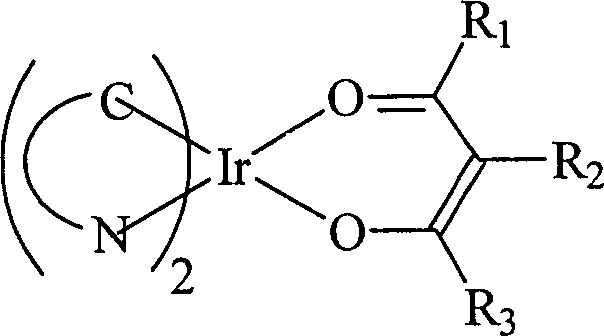
Hierbei ist C⌒N ein zumindest zweizähniger Ligand, der mit dem Metall-Atom einen metallacyclischen Ring bildet. Die Bezeichnung ”C⌒N” steht weiters für einen Liganden, bei dem an das Iridium-Atom einerseits eine Koordination über ein Kohlenstoff-Atom und andererseits über ein Stickstoff-Atom erfolgt. Sowohl das Kohlenstoff-Atom als auch das Stickstoff-Atom liegen dabei üblicherweise in einem aromatischen Ringsystem vor. Im Fall des Kohlenstoff-Atoms ist dies zumeist ein homocyclischer aromatischer Ring. Unabhängig davon ist der über das Stickstoff-Atom an das Iridium-Atom koordinierte Ring üblicherweise ein heterocyclischer Ring, der neben dem Stickstoff-Atom kein weiteres oder nur ein weiteres Hetero-Atom (insbesondere ein weiteres Stickstoff-Atom oder ein Sauerstoff-Atom) enthält.In this case, C⌒N is an at least bidentate ligand which forms a metallacyclic ring with the metal atom. The term "C⌒N" further stands for a ligand in which the iridium atom is coordinated on the one hand by a carbon atom and on the other hand by a nitrogen atom. Both the carbon atom and the nitrogen atom are usually present in an aromatic ring system. In the case of the carbon atom, this is usually a homocyclic aromatic ring. Independently of this, the ring coordinated via the nitrogen atom to the iridium atom is usually a heterocyclic ring which, in addition to the nitrogen atom, contains no further or only one further heteroatom (in particular a further nitrogen atom or an oxygen atom) ,
Die zwei C⌒N-Liganden können hierbei zusammen auch einen vierzähnigen Liganden bilden; ebenso ist eine Verbrückung des anderen Liganden (einem Acetylacetonat-Derivat) mit einem oder beiden der C⌒N-Liganden möglich. Im Acetylacetonat-Derivat stehen die Reste R1, R2 und R3 unabhängig voneinander für verzweigte, unverzweigte kondensierte und/oder ringförmige Alkylreste und/oder für Arylreste, es kann sich insbesondere um das Acetylacetonat selbst handeln. Sowohl die Arylreste als auch die Alkylreste können vollständig oder teilweise mit funktionellen Gruppen (beispielsweise Ether-Gruppen (etwa Metoxy-, Etoxy- oder Propoxy-Gruppen), Ester-Gruppen, Amid-Gruppen oder auch Carbonat-Gruppen) substituiert sein. Der Rest R2 kann auch Wasserstoff oder Fluor sein. Häufig werden die Reste R1 und R2 Methyl, Ethyl oder Propyl sein und gegebenenfalls auch Phenyl. R2 wird häufig Wasserstoff oder Fluor sein. Die genannten Ethyl-, Methyl-, Propyl- und Phenyl-Gruppen liegen dabei entweder unsubstituiert vor oder weisen einen oder mehrere Fluor-Substituenten auf. Die zuletzt genannten Verbindungen sind synthetisch einfach zu erhalten bzw. käuflich. Die Einführung von Fluor-Substituenten erleichtert im Regelfall die Verdampfbarkeit der Komplexe mit derartigen Liganden und führt zudem häufig zu einer Verschiebung der Emission zu kürzeren Wellenlängen.The two C⌒N ligands can together also form a tetradentate ligand; it is also possible to bridge the other ligand (an acetylacetonate derivative) with one or both of the C⌒N ligands. In the acetylacetonate derivative, the radicals R 1 , R 2 and R 3 are each independently branched, unbranched condensed and / or cyclic alkyl radicals and / or aryl radicals, it may be in particular the acetylacetonate itself. Both the aryl radicals and the alkyl radicals may be completely or partially substituted with functional groups (for example ether groups (for example metoxy, ethoxy or propoxy groups), ester groups, amide groups or else carbonate groups). The radical R 2 can also be hydrogen or fluorine. Frequently, the radicals R 1 and R 2 will be methyl, ethyl or propyl and optionally also phenyl. R 2 will often be hydrogen or fluorine. The said ethyl, methyl, propyl and phenyl groups are either unsubstituted or have one or more fluorine substituents. The latter compounds are synthetically easy to obtain or commercially available. The introduction of fluorine substituents usually facilitates the vaporizability of the complexes with such ligands and also often results in a shift of the emission to shorter wavelengths.
Gemäß einer weiteren Ausführungsform bildet der Ligand C⌒N mit dem Iridium-Atom einen fünf-gliedrigen oder sechsgliedrigen metallacyclischen Ring. Insbesondere kann der Ligand C⌒N Phenylpyridin, Phenylimigazol, Phenyloxazol, Benzylpyridin, Benzylimidazol oder Benzyloxazol sein oder ein Ligand, der eine der genannten Verbindungen als Grundgerüst aufweist, bei dem also die entsprechende heterocyclische Grundstruktur enthalten ist, bei dem allerdings zusätzliche Substituenten, Verbrückungen oder annelierte Ringe vorhanden sind. Als Substituenten kommen insbesondere Fluoratome in Betracht, da durch Substitution mit einem oder mehreren Fluoratomen einer Verschiebung der Emissionswellenlänge in den blauen Spektralbereich (430–500 nm) oder gar den violetten Spektralbereich (380–430 nm) erreichen lässt. Ferner können als Substituenten für verzweigte, unverzweigte kondensierte und/oder ringförmige Alkylreste und/oder Arylreste sowie funktionellen Gruppen (beispielsweise Ether-Gruppen (etwa Metoxy-, Etoxy- oder Propoxy-Gruppen), Ester-Gruppen, Amid-Gruppen oder auch Carbonat-Gruppen) enthalten sein.In another embodiment, the ligand C⌒N with the iridium atom forms a five-membered or six-membered metallacyclic ring. In particular the ligand C⌒N can be phenylpyridine, phenylimigazole, phenyloxazole, benzylpyridine, benzylimidazole or benzyloxazole or a ligand which has one of the abovementioned compounds as the basic skeleton, ie which contains the corresponding heterocyclic basic structure but in which additional substituents, bridges or annelated rings are present. Particularly suitable substituents are fluorine atoms, since substitution with one or more fluorine atoms makes it possible to shift the emission wavelength into the blue spectral range (430-500 nm) or even the violet spectral range (380-430 nm). Furthermore, as substituents for branched, unbranched condensed and / or cyclic alkyl radicals and / or aryl radicals and also functional groups (for example ether groups (for example metoxy, ethoxy or propoxy groups), ester groups, amide groups or else carbonate radicals Groups).
Mit den Liganden gemäß dieser Ausführungsform lassen sich oft besonders große Übergangsdipolmomente erzielen.With the ligands according to this embodiment, particularly large transition dipole moments can often be achieved.
Gemäß einer weiteren Ausführungsform weist der Ligand C⌒N mindestens drei zumindest zum Teil kondensierte aromatische Ringe auf. Häufig wird der Ligand sogar vier oder mehr zumindest zum Teil kondensierte aromatische Ringe aufweisen. ”Zumindest zum Teil kondensiert” bedeutet hierbei, dass ein oder auch mehrere kondensierte Ringsysteme im Liganden C⌒N vorliegen können. Beispielsweise kann der Ligand durch drei miteinander kondensierte aromatische Ringe gebildet sein, an die eine Phenyl-Gruppe oder eine Benzyl-Gruppe angebunden ist. Liegt mehr als ein Ringsystem im Liganden vor, so kann der kondensierte aromatische Ring sowohl an den Stickstoffheterozyklus als auch an den homocyclischen Aromaten kondensiert sein oder auch an beide Ringe kondensiert sein.According to another embodiment, the ligand C⌒N has at least three at least partially condensed aromatic rings. Frequently, the ligand will even have four or more at least partially fused aromatic rings. "At least partially condensed" here means that one or more condensed ring systems can be present in the ligand C⌒N. For example, the ligand may be formed by three fused aromatic rings to which a phenyl group or a benzyl group is attached. If there is more than one ring system in the ligand, the fused aromatic ring may be fused to both the nitrogen heterocycle and the homocyclic aromatics or may be fused to both rings.
Als Emittermaterialien kommen insbesondere folgende Verbindungen in Betracht, die ein Emissionsmaximum im blauen, grünen oder roten Spektralbereich aufweisen:
Ir(ppy)2(acac) = (Bis(2-phenylpyridin)(acetylacetonat)iridium(II)), Ir(mppy)2(acac) = (Bis[2-(p-tolyl)pyridin]acetylacetonat)iridium(III)), Bis[1-(9,9-dimethyl-9H-fluoren-2-yl)-isochinolin](acetylacetonat)iridium(III), Ir(mdq)2(acac) = (Bis(2-methyl-dibenzo[f,h]-chinoxalin)(acetylacetonat)iridium(III)), Iridium(III)-bis(dibenzo[f,h]chinoxalin)(acetylacetonat), Ir(btp)2(acac) = (Bis(2-benzo[b]thiophen-2-yl-pyridin)(acetylacetonat)iridium(III)), Ir(piq)2(acac) = (Bis(1-phenylisochinolin)(acetylacetonat)iridium(III)), Ir(fliq)2(acac)-1 = (Bis[1-(9,9-dimethyl-9H-fluoren-2-yl)-isochinolin](acetylacetonat)iridium(III)), Hex-Ir(phq)2(acac) = Bis[2-(4-n-hexylphenyl)chinolin](acetylacetonat)iridium(III), Ir(flq)2(acac)-2 = (Bis[3-(9,9-dimethyl-9H-fluoren-2-yl)-isochinolin](acetylacetonat)iridium(III)), Bis[2-(9,9-dibutylfluorenyl)-1-isochinolin](acetylacetonat)iridium(III), Bis[2-(9,9-dihexylfluorenyl)-1-pyridin](acetylacetonat)iridium(III), (fbi)2Ir(acac) = Bis(2-(9,9-diethyl-fluoren-2-yl)-1-phenyl-1H-benzo[d]imidazolato)(acetylacetonat)iridium(III), Ir(2-phq)2(acac) = (Bis(2-phenylchinolin)(acetylacetonat)iridium(III)), Iridium(III)-bis(2-(2'-benzothienyl)pyridinato-N,C3')(acetylacetonat), Ir(BT)2(acac) = Bis(2-phenylbenzothiazolat) (acetylacetonat)iridium(III), (PQ)2Ir(dpm) = Bis(2-phenylchinolin)(2,2,6,6-tetramethylheptan-3,5-dionat)iridium(III), (Piq)2Ir(dpm) = Bis(phenylisochinolin)(2,2,6,6-tetramethylheptan-3,5-dionat)iridium(III) und Iridium(III) bis (4-phenylthieno[3,2-c]pyridinato-N,C2')acetylacetonat sowie Gemische der vorgenannten Stoffe. Für Emittermaterialien, die im blauen Wellenlängenbereich emittieren kommen beispielsweise Carbenkomplexe des Iridiums in Betracht. Die Bezeichnung ”C⌒N” steht dann also für einen Liganden, bei dem an das Iridium-Atom eine Koordination über ein Carben-Kohlenstoff-Atom und ein Stickstoff-Atom erfolgt.Suitable emitter materials are, in particular, the following compounds which have an emission maximum in the blue, green or red spectral range:
Ir (ppy) 2 (acac) = (bis (2-phenylpyridine) (acetylacetonate) iridium (II)), Ir (mppy) 2 (acac) = (bis [2- (p-tolyl) pyridine] acetylacetonate) iridium ( III)), bis [1- (9,9-dimethyl-9H-fluoren-2-yl) isoquinoline] (acetylacetonate) iridium (III), Ir (mdq) 2 (acac) = (bis (2-methyl) dibenzo [f, h] -quinoxaline) (acetylacetonate) iridium (III)), iridium (III) bis (dibenzo [f, h] quinoxaline) (acetylacetonate), Ir (btp) 2 (acac) = (bis (2 benzo [b] thiophen-2-yl-pyridine) (acetylacetonate) iridium (III)), Ir (piq) 2 (acac) = (bis (1-phenylisoquinoline) (acetylacetonate) iridium (III)), Ir (fliq ) 2 (acac) -1 = (bis [1- (9,9-dimethyl-9H-fluoren-2-yl) -isoquinoline] (acetylacetonate) iridium (III)), Hex-Ir (phq) 2 (acac) = Bis [2- (4-n-hexylphenyl) quinoline] (acetylacetonate) iridium (III), Ir (flq) 2 (acac) -2 = (bis [3- (9,9-dimethyl-9H-fluorene-2 -yl) -isoquinoline] (acetylacetonate) iridium (III)), bis [2- (9,9-dibutylfluorenyl) -1-isoquinoline] (acetylacetonate) iridium (III), bis [2- (9,9-dihexylfluorenyl) 1-pyridine] (acetylacetonate) iridium (III), (fbi) 2 Ir (acac) = bis (2- (9,9-diethyl fluoren-2-yl) -1-phenyl-1H-benzo [d] imidazolato) (acetylacetonate) iridium (III), Ir (2-phq) 2 (acac) = (bis (2-phenylquinoline) (acetylacetonate) iridium (III)), iridium (III) bis (2- (2'-benzothienyl) pyridinato-N, C3 ') (acetylacetonate), Ir (BT) 2 (acac) = bis (2-phenylbenzothiazolate) (acetylacetonate) iridium (III), (PQ) 2 Ir (dpm) = bis (2-phenylquinoline) (2,2,6,6-tetramethylheptane-3,5-dionate) iridium (III), (Piq) 2 Ir (dpm) = Bis (phenylisoquinoline) (2,2,6,6-tetramethylheptane-3,5-dionate) iridium (III) and iridium (III) bis (4-phenylthieno [3,2-c] pyridinato-N, C2 ') acetylacetonate and mixtures of the aforementioned substances. For emitter materials that emit in the blue wavelength range, for example, carbene complexes of iridium come into consideration. The term "C⌒N" then stands for a ligand in which the iridium atom is coordinated by a carbene carbon atom and a nitrogen atom.
Gemäß einer weiteren Ausführungsform kann neben dem phosphoreszenten Metallkomplex auch das Matixmaterial eine anisotrope Molekülstruktur aufweisen. Mittels derartiger Matrixmaterialien kann eine anisotrope Ausrichtung der phosphoreszenten Metallkomplexe zusätzlich unterstützt werden.According to a further embodiment, in addition to the phosphorescent metal complex, the Matix material may also have an anisotropic molecular structure. By means of such matrix materials, an anisotropic alignment of the phosphorescent metal complexes can be additionally supported.
Entsprechend zu den anisotropen phosphoreszenten Metallkomplexen gilt auch für das Matrixmaterial mit anisotroper Molekülstruktur, dass hier insbesondere keine im Wesentlichen symmetrisch substituierten Verknüpfungspunkte vorliegen dürfen, wie etwa ein in eins, drei und fünf Position (symmetrisch) substitutierter aromatischer Sechsring oder ein tertiäres Amin mit jeweils drei gleichen Substituenten.Corresponding to the anisotropic phosphorescent metal complexes, the matrix material having an anisotropic molecular structure also does not have any substantially symmetrically substituted attachment points, such as one in three, three and five position (symmetrically) substituted aromatic six-membered ring or a tertiary amine of three each same substituents.
Insbesondere wird unter einem Matrixmaterial mit anisotroper Molekülstruktur ein Material verstanden, bei dem ausgehend von einer zentralen Verzweigungsstelle, insbesondere einem zentralen Atom oder einem zentralen Ring, keine drei, vier oder mehr Substituenten mit gleicher oder im Wesentlichen gleicher Struktur vorliegen (wobei nur Substituenten beachtet werden, die nicht Wasserstoff sind). Eine gleiche Struktur bedeutet dabei, dass die Substituenten identisch sind; eine im Wesentlichen gleiche Struktur bedeutet ferner, dass sich die mindestens drei Substituenten hinsichtlich des auf sie entfallenden Molekulargewichts zwar unterscheiden, dass bei aber bei keinem der Substituenten der Verzweigungsstelle ein Molekulargewicht vorliegt, das um zumindest 50% unter einem der anderen Substituenten liegt (wobei nur Substituenten beachtet werden, die nicht Wasserstoff sind). Dementsprechend sind Moleküle mit anisotroper Molekülstruktur keine hochsymmetrischen Moleküle mit mehr als zwei gleichen Substituenten oder sie weisen bei Verzweigungsstellen mit drei oder mehr Substituenten (z. B. Verzweigungsstellen wie tertiären Amin-Stickstoffatomen oder zumindest dreifach substituierten Benzol-Ringen) sehr unterschiedliche Substituenten auf.In particular, a matrix material with anisotropic molecular structure is understood as meaning a material in which, starting from a central branching point, in particular a central atom or a central ring, there are no three, four or more substituents having the same or substantially the same structure (only substituents being taken into account that are not hydrogen). A similar structure means that the substituents are identical; A substantially similar structure further means that although the at least three substituents differ in the molecular weight attributed thereto, none of the substituents of the branching site has a molecular weight which is at least 50% lower than any of the other substituents (only Note substituents that are not hydrogen). Accordingly, molecules of anisotropic molecular structure are not highly symmetric molecules having more than two equal substituents or have very different substituents at branching sites having three or more substituents (eg, branching sites such as tertiary amine nitrogen atoms or at least trisubstituted benzene rings).
Die vorstehend definierte Verzweigungsstelle ist insbesondere die Verzweigungsstelle, die dem Molekülschwerpunkt am nächsten liegt. Der Molekülschwerpunkt ist zwar aufgrund möglicher Rotationen von Teilbereichen des Moleküls aufwändig zu bestimmen; allerdings ist es für den Fachmann bei den meisten Molekülen ohne Berechnung vollkommen klar, welche Verzweigungsstelle in einem Molekül dem Schwerpunkt am nächsten liegt, da für die Bestimmung näherungsweise auch der Schwerpunkt ausreicht, der sich ergeben würde, wenn für alle Atome angenommen werden würde, dass sie tatsächlich nur zweidimensional in der Papierebene angeordnet sind.The branching point defined above is in particular the branching point which is closest to the molecular center of gravity. Although the molecular center of gravity is difficult to determine due to possible rotations of partial regions of the molecule; however, it is perfectly clear to a person skilled in the art for most molecules without calculation which branch point in a molecule is closest to the center of gravity, since the center of gravity that would result if all atoms were assumed to be sufficient for the determination would be approximately sufficient they are actually arranged only two-dimensionally in the paper plane.
Gemäß einer weiteren Ausführungsform wird das Matrixmaterial in Schritt A) aus Verbindungen des Typs A-K-B ausgewählt.According to a further embodiment, the matrix material in step A) is selected from compounds of the type A-K-B.
Hierbei steht das Strukturelement K für eine Struktur Ar1-X-Ar2, die insbesondere kettenartig ist. Hierbei stehen Ar1 und Ar2 für gleiche oder verschiedene aromatische Ringe und X für eine Einfachbindung, eine weitere aromatische Gruppe oder für eine Verknüpfung (von Ar1 und Ar2) mittels eines annelierten (bzw. kondensierten) Rings, also eines Rings, mit dem beide Reste Ar1 und Ar2 miteinander kondensiert sind.Here, the structural element K stands for a structure Ar 1 -X-Ar 2 , which is in particular like a chain. Here, Ar 1 and Ar 2 are identical or different aromatic rings and X is a single bond, another aromatic group or a linkage (of Ar 1 and Ar 2 ) by means of a fused (or condensed) ring, so a ring with the two radicals Ar 1 and Ar 2 are condensed together.
Ferner sind auch die Strukturelemente A und B gleich oder verschieden und umfassen jeweils zumindest einen aromatischen Ring, insbesondere einen aromatischen Ring, der an das Strukturelement K direkt oder mittelbar (d. h. verknüpft über weitere Atome oder Gruppen) gebunden ist.Furthermore, the structural elements A and B are identical or different and each comprise at least one aromatic ring, in particular an aromatic ring, which is bonded to the structural element K directly or indirectly (i.e., linked via further atoms or groups).
Die Gruppen Ar1, Ar2 und X (falls es eine aromatische Gruppe darstellt) können unsubstituierte oder beliebig substituierte aromatische Verbindungen sein, insbesondere sind die Substituenten aber ausgewählt aus sterisch wenig anspruchsvollen Gruppen. Im Regelfall werden die aromatischen Ringe Ar1, Ar2 und X daher keine Substituenten aufweisen, deren Kohlenstoff-Atome zwingend nicht in der Ebene zu liegen kommen, die durch den aromatischen Ring aufgespannt ist, und meist auch keine Substituenten, die zumindest teilweise (räumlich und/oder zeitlich) nicht in der durch den Aromaten aufgespannten Ebene liegen. Entsprechendes gilt auch für Substituenten des Strukturelements X, sofern es sich um eine nicht aromatische Verbrückung der aromatischen Ring Ar1 und Ar2 handelt. Hier kann eine etwaige Alkylen-Verknüpfung (wie sie beispielsweise in einer durch die Struktur Ar1-X-Ar2 beschriebenen Fluoren-Gruppe vorliegt) ebenfalls beliebig substituiert sein. Allerdings wird es sich aus sterischen Gründen bei den Substituenten häufig nur um sterisch wenig anspruchsvolle Substituenten wie Methyl-, Ethyl- oder Propyl-Gruppen oder um cyclische bzw. spirocyclische Alkylengruppen handeln oder um Gruppen, die sterisch einen Platzbedarf haben, der dem der genannten Gruppen entspricht oder geringer ist (beispielsweise Metoxy-Gruppen). Im Ausnahmefall kann, insbesondere bei entsprechend ausladenden Substituenten der Gruppen A und B auch eine Phenyl-Gruppe an eine derartige Alkylen-(beispielsweise Methylen-)Gruppe gebunden sein.The groups Ar 1 , Ar 2 and X (if it represents an aromatic group) can unsubstituted or arbitrarily substituted aromatic compounds, but in particular the substituents are selected from sterically less demanding groups. As a rule, the aromatic rings Ar 1 , Ar 2 and X will therefore not have any substituents whose carbon atoms do not necessarily lie in the plane which is spanned by the aromatic ring, and usually also no substituents which are at least partially (spatially and / or temporally) are not in the plane defined by the aromatic. The same applies to substituents of the structural element X, provided that it is a non-aromatic bridge of the aromatic ring Ar 1 and Ar 2 . Here, any alkylene linkage (as present, for example, in a fluorene group described by the structure Ar 1 -X-Ar 2 ) may also be substituted as desired. However, for steric reasons, the substituents will often only be sterically less demanding substituents, such as methyl, ethyl or propyl groups, or cyclic or spiro-cyclic alkylene groups or groups which have a steric need of space, that of the groups mentioned is equal to or less (for example, metoxy groups). In exceptional cases, in particular with correspondingly bulky substituents of groups A and B, a phenyl group may also be bonded to such an alkylene (for example methylene) group.
Die Struktur Ar1-X-Ar2 ist insbesondere kettenartig ausgebildet. Hierbei heißt kettenartig, dass die zwei bzw. drei Ringe dieses Strukturelements in Bezug auf die Strukturelemente A und B so aneinander gebunden sind, dass die Gruppen A und X (bzw. A und Ar2 für den Fall, dass X eine Bindung oder einen an Ar1 und Ar2 annelierten Ring darstellt) in Para-Position zueinander angeordnet sind. Dieselbe Strukturbeziehung gilt ebenfalls für die Anordnung der Gruppen B und X bzw. B und Ar1. Zusätzlich können allerdings weitere Verknüpfungen insbesondere zwischen den Ringen Ar1 und Ar2 vorliegen, wie sie beispielsweise ohnehin im Fall eines an Ar1 und Ar2 annelierten Rings X vorhanden sind.The structure Ar 1 -X-Ar 2 is designed in particular like a chain. Here, in a chain-like manner, the two or three rings of this structural element are bonded to one another in relation to the structural elements A and B such that the groups A and X (or A and Ar 2, respectively, in the case where X is a bond or an Ar 1 and Ar 2 are annulated ring) are arranged in para-position to each other. The same structural relationship also applies to the arrangement of groups B and X or B and Ar 1 . In addition, however, further linkages may in particular be present between the rings Ar 1 and Ar 2 , as they are present, for example, anyway in the case of a ring X fused to Ar 1 and Ar 2 .
Durch Auswahl eines Matrixmaterials mit einem Strukturelement K, das, wie aus den vorstehenden Ausführungen deutlich wird, eher planar als kugelförmig ausgebildet ist, kann ein Material zur Verfügung gestellt werden, was eine ausgeprägte Anisotropie zeigt und sich daher besonders gut für das erfindungsgemäße Verfahren eignet. Wesentlich hierbei ist, dass die Verknüpfung der Strukturelemente A, K und B gewissermaßen kettenförmig ist, wodurch erreicht wird, dass die Moleküle in Bezug auf die durch die Gruppen A, K und B verlaufende Längsachse deutlich länger ist als die Ausdehnung des Moleküls in den Richtungen orthogonal zu dieser Achse, insbesondere so weit der Bereich des Strukturelements K betroffen ist.By selecting a matrix material with a structural element K, which, as is clear from the above explanations, is more planar than spherical, a material can be provided which shows pronounced anisotropy and is therefore particularly suitable for the method according to the invention. It is essential here that the linkage of the structural elements A, K and B is to a certain extent chain-shaped, whereby it is achieved that the molecules with respect to the longitudinal axis passing through the groups A, K and B are significantly longer than the extent of the molecule in the directions orthogonal to this axis, in particular as far as the area of the structural element K is concerned.
Gemäß einer weiteren Ausführungsform weist daher das Strukturelement K keine spirocyclische Gruppe mit mehr als fünf Kohlenstoffatomen auf, insbesondere keine derartige Gruppe, bei der eine Alkylen-Gruppe, die die Ringe Ar1 und Ar2 miteinander verbindet, einen spirocyclischen Ring als Substituenten trägt, der direkt an die Alkylen-Gruppe gebunden ist. Auch hierdurch kann unterbunden werden, dass das mittlere Strukturelement K des Matrixmaterials zu ausladend wird.According to a further embodiment, therefore, the structural element K has no spirocyclic group having more than five carbon atoms, in particular no such group in which an alkylene group which connects the rings Ar 1 and Ar 2 together, carries a spirocyclic ring as a substituent which is bonded directly to the alkylene group. This also prevents the middle structural element K of the matrix material from becoming too bulky.
Gemäß einer weiteren Ausführungsform stehen die Gruppen Ar1 und Ar2 des Strukturelements K jeweils für einen Stickstoffhaltigen Heterocyclus und können beispielsweise ein Biphenyl-, ein Phenanthrolin-, ein Pyridin-, ein Bipyridin- und/oder ein Pyrimidin-Derivat umfassen. Ferner kann unabhängig hiervon sowohl das Strukturelement A als auch das Strukturelement B des Matrixmaterials A-K-B eine aromatisch substituierte Amingruppe umfassen, insbesondere eine aromatisch substituierte Amingruppe, die direkt an das Strukturelement K gebunden ist. Insbesondere kann das Matrixmaterial in diesem Fall ein Benzidin-Derivat umfassen.According to a further embodiment, the groups Ar 1 and Ar 2 of the structural element K are each a nitrogen-containing heterocycle and may for example comprise a biphenyl, a phenanthroline, a pyridine, a bipyridine and / or a pyrimidine derivative. Furthermore, independently of this, both the structural element A and the structural element B of the matrix material AKB may comprise an aromatic-substituted amine group, in particular an aromatic-substituted amine group which is bonded directly to the structural element K. In particular, the matrix material in this case may comprise a benzidine derivative.
Derartige Matrixmaterialien weisen also ein eher flächiges zentrales Segment in Form der Benzidin-Gruppe bzw. der Phenanthrolin-Gruppe auf, sodass eine anisotrope Molekülstruktur erreicht werden kann.Thus, such matrix materials have a more planar central segment in the form of the benzidine group or the phenanthroline group, so that an anisotropic molecular structure can be achieved.
Gemäß einer weiteren Ausführungsform können auch die Strukturelemente A und B des Matrixmaterials so ausgebildet werden, dass eine besonders anisotrope Molekülstruktur resultiert. Hierzu können gewissermaßen an den ”Enden” eines eher langgestreckten Moleküle sterisch anspruchsvolle Substituenten vorgesehen werden. Die Strukturelemente A und B können daher beispielsweise einen substituierten Aromaten umfassen, der eine tertiäre Alkyl-Gruppe trägt (insbesondere in para-Stellung). Enthalten die Strukturelemente A und B jeweils ein Stickstoff-Atom, das direkt an Strukturelement K gebunden ist, so kann nur einer der zwei terminalen Substituenten des Stickstoff-Atoms oder auch beide terminalen Substituenten eine derartige substituierte aromatische Gruppe tragen. Statt einer mit einer tertiären Alkyl-Gruppe substituierten aromatischen Gruppe kann auch eine polycyclische Aryl-Gruppe, in der zumindest zwei aromatische Ringe aneinander kondensiert sind, als sterisch anspruchsvolle Gruppe vorliegen. Beispielsweise sind hierbei Naphtyl-Gruppen zu nennen.According to a further embodiment, the structural elements A and B of the matrix material can also be formed so that a particularly anisotropic molecular structure results. To this end, sterically demanding substituents can, as it were, be provided at the "ends" of a rather elongated molecule. The structural elements A and B can therefore comprise, for example, a substituted aromatic which carries a tertiary alkyl group (in particular in the para position). If the structural elements A and B each contain a nitrogen atom which is bonded directly to structural element K, only one of the two terminal substituents of the nitrogen atom or else both terminal substituents can carry such a substituted aromatic group. Instead of an aromatic group substituted with a tertiary alkyl group, a polycyclic aryl group in which at least two aromatic rings are fused to each other can also be present as a sterically demanding group. For example, naphthyl groups are mentioned here.
Gemäß einer weiteren Ausführungsform kann das Matrixmaterial lochtransportierende und/oder elektronentransportierende Eigenschaften aufweisen. Emittiert der phosphoreszente Emitter im violetten, blauen oder grünen Spektralbereich (also insbesondere bei einer Wellenlänge < 570 nm), so wird häufig ein elektronentransportierendes Matrixmaterial gewählt, weil dies im Regelfall aufgrund der Lage der Triplett-Niveaus des Matrixmaterials und des Emitter-Materials günstiger ist.According to a further embodiment, the matrix material may have hole-transporting and / or electron-transporting properties. If the phosphorescent emitter emits in the violet, blue or green spectral range (that is to say in particular at a wavelength <570 nm), then Often an electron-transporting matrix material is chosen because this is generally more favorable due to the location of the triplet levels of the matrix material and the emitter material.
Gemäß einer weiteren Ausführungsform kann das Matrixmaterial aus einer oder mehreren der nachfolgenden Verbindungen ausgewählt sein oder zumindest eine der genannten Verbindungen umfassen:
Als Elektronentransportmaterialien seien beispielsweise PBD (2-(4-Biphenylyl)-5-(4-tert-butylphenyl)-1,3,4-oxadiazol), BCP (2,9-Dimethyl-4,7-diphenyl-1,10-phenanthrolin), BPhen (4,7-Diphenyl-1,10-phenanthrolin), TAZ (3-(4-Biphenylyl)-4-phenyl-5-tert-butylphenyl-1,2,4-triazol), Bpy-OXD (1,3-Bis[2-(2,2'-bipyrid-o-yl)-1,3,4-oxadiazol-5-yl]benzol), BP-OXD-Bpy (6,6'-Bis[5-(biphenyl-4-yl)-1,3,4-oxadiazol-2-yl]-2,2'-bipyridyl), PADN (2-phenyl-9,10-di(naphth-2-yl)-anthracene), Bpy-FOXD (2,7-Bis[2-(2,2'-bipyrid-6-yl)-1,3,4-oxadiazol-5-yl]-9,9-dimethylfluoren), OXD-7 (1,3-Bis[2-(4-tert-butylphenyl)-1,3,4-oxadiazol-5-yl]benzol), HNBphen (2-(naphth-2-yl)-4,7-diphenyl-1,10-phenanthrolin), NBphen (2,9-Bis(naphth-2-yl)-4,7-diphenyl-1,10-phenanthrolin), und 2-NPIP (1-methyl-2-(4-(naphth-2-yl)phenyl)-1H-imidazo[4,5-f][1,10]phenanthrolin) sowie Gemische der vorgenannten Stoffe genannt.According to a further embodiment, the matrix material may be selected from one or more of the following compounds or comprise at least one of the compounds mentioned:
Examples of suitable electron transport materials are PBD (2- (4-biphenylyl) -5- (4-tert-butylphenyl) -1,3,4-oxadiazole), BCP (2,9-dimethyl-4,7-diphenyl-1,10 phenanthroline), BPhen (4,7-diphenyl-1,10-phenanthroline), TAZ (3- (4-biphenylyl) -4-phenyl-5-tert-butylphenyl-1,2,4-triazole), Bpy- OXD (1,3-bis [2- (2,2'-bipyrid-o-yl) -1,3,4-oxadiazol-5-yl] benzene), BP-OXD-Bpy (6,6'-bis [5- (biphenyl-4-yl) -1,3,4-oxadiazol-2-yl] -2,2'-bipyridyl), PADN (2-phenyl-9,10-di (naphth-2-yl) -anthracenes), Bpy-FOXD (2,7-bis [2- (2,2'-bipyrid-6-yl) -1,3,4-oxadiazol-5-yl] -9,9-dimethylfluorene), OXD -7 (1,3-bis [2- (4-tert-butylphenyl) -1,3,4-oxadiazol-5-yl] benzene), HNBphen (2- (naphth-2-yl) -4,7- diphenyl-1,10-phenanthroline), NBphen (2,9-bis (naphth-2-yl) -4,7-diphenyl-1,10-phenanthroline), and 2-NPIP (1-methyl-2- (4 - (naphth-2-yl) phenyl) -1H-imidazo [4,5-f] [1,10] phenanthroline) and mixtures of the aforementioned substances.
Als Lochtransportmaterialien seien zum Beispiel NPB (N,N'-Bis(naphth-1-yl)-N,N'-bis(phenyl)-benzidin, β-NPB (N,N'-Bis(naphth-2-yl)-N,N'-bis(phenyl)-benzidin), TPD (N,N'-Bis(3-methylphenyl)-N,N'-bis(phenyl)-benzidin), N,N'-Bis(naphth-1-yl)-N,N'-bis(phenyl)-2,2-dimethylbenzidin, DMFL-TPD (N,N'-Bis(3-methylphenyl)-N,N'-bis(phenyl)-9,9-dimethylfluoren, DMFL-NPB (N,N'-Bis(naphth-1-yl)-N,N'-bis(phenyl)-9,9-dimethylfluoren), DPFL-TPD (N,N'-Bis(3-methylphenyl)-N,N'-bis(phenyl)-9,9-diphenylfluoren), DPFL-NPB (N,N'-Bis(naphth-1-yl)-N,N'-bis(phenyl)-9,9-diphenylfluoren), TAPC (Di-[4-(N,N-ditolyl-amino)-phenyl]cyclohexan), PAPB (N,N'-bis(phenanthren-9-yl)-N,N'-bis(phenyl)-benzidin), TNB (N,N,N',N'-tetra-naphth-2-yl-benzidin), TiOPC (Titanoxide phthalocyanin), CuPC (Kupfer-Phthalocyanin), F4-TCNQ (2,3,5,6-Tetrafluor-7,7,8,8,-tetracyano-chinodimethan), PPDN (Pyrazino[2,3-f][1,10]phenanthrolin-2,3-dicarbonitril), MeO-TPD (N,N,N',N'-Tetrakis(4-methoxyphenyl)benzidin), β-NPP (N,N'-di(naphth-2-yl)-N,N'-diphenylbenzol-1,4-diamin), NTNPB (N,N'-di-phenyl-N,N'-di-[4-(N,N-di-tolyl-amino)phenyl]benzidin) und NPNPB (N,N'-di-phenyl-N,N'-di-[4-(N,N-diphenyl-amino)phenyl]benzidin), 1,4-bis(2-phenylpyrimidin-5-yl)benzen (BPPyP), 1,4-bis(2-methylpyrimidin-5-yl)benzen (BMPyP), 1,4-di(1,10-phenanthrolin-3-yl)benzen (BBCP), 2,5-di(pyridin-4-yl)pyrimidin (DPyPy), 1,4-bis(2-(pyridin-4-yl)pyrimidin-5-yl)benzen (BPyPyP), 2,2',6,6'-tetraphenyl-4,4'-bipyridin (GBPy), 1,4-di(benzo[h]chinolin-3-yl)benzol (PBAPA), 2,3,5,6-tetraphenyl-4,4'-bipyridin (TPPyPy), 1,4-bis(2,3,5,6-tetraphenylpyridin-4-yl)benzen (BTPPyP), 1,4-bis(2,6-tetrapyridinylpyridin-4-yl)benzen (BDPyPyP) oder Gemische der vorgenannten Stoffe genannt.Examples of suitable hole-transporting materials are NPB (N, N'-bis (naphth-1-yl) -N, N'-bis (phenyl) -benzidine, β-NPB (N, N'-bis (naphth-2-yl) N, N'-bis (phenyl) benzidine), TPD (N, N'-bis (3-methylphenyl) -N, N'-bis (phenyl) benzidine), N, N'-bis (naphthenic) 1-yl) -N, N'-bis (phenyl) -2,2-dimethylbenzidine, DMFL-TPD (N, N'-bis (3-methylphenyl) -N, N'-bis (phenyl) -9.9 dimethylfluorene, DMFL-NPB (N, N'-bis (naphth-1-yl) -N, N'-bis (phenyl) -9,9-dimethylfluorene), DPFL-TPD (N, N'-bis (3 -methylphenyl) -N, N'-bis (phenyl) -9,9-diphenylfluorene), DPFL-NPB (N, N'-bis (naphth-1-yl) -N, N'-bis (phenyl) -9 , 9-diphenylfluorene), TAPC (di- [4- (N, N-ditolylamino) -phenyl] cyclohexane), PAPB (N, N'-bis (phenanthren-9-yl) -N, N'-bis (phenyl) benzidine), TNB (N, N, N ', N'-tetra-naphth-2-yl-benzidine), TiOPC (titanium oxide phthalocyanine), CuPC (copper phthalocyanine), F4-TCNQ (2,3 , 5,6-tetrafluoro-7,7,8,8-tetracyanoquinodimethane), PPDN (pyrazino [2,3-f] [1,10] phenanthroline-2,3-dicarbonitrile), MeO-TPD (N , N, N ', N'-tetrakis (4-methoxyphenyl) benzidine), β-NPP (N, N'-di (naphth-2-yl) -N, N '-diphenylbenzene-1,4-diamine), NTNPB (N, N'-di-phenyl-N, N'-di- [4- (N, N-di-tolyl-amino) -phenyl] -benzidine) and NPNPB ( N, N'-di-phenyl-N, N'-di- [4- (N, N-diphenylamino) phenyl] benzidine), 1,4-bis (2-phenylpyrimidin-5-yl) benzene (BPPyP ), 1,4-bis (2-methylpyrimidin-5-yl) benzene (BMPyP), 1,4-di (1,10-phenanthrolin-3-yl) benzene (BBCP), 2,5-di (pyridine) 4-yl) pyrimidine (DPyPy), 1,4-bis (2- (pyridin-4-yl) pyrimidin-5-yl) benzene (BPyPyP), 2,2 ', 6,6'-tetraphenyl-4,4 '-bipyridine (GBPy), 1,4-di (benzo [h] quinolin-3-yl) benzene (PBAPA), 2,3,5,6-tetraphenyl-4,4'-bipyridine (TPPyPy), 1, 4-bis (2,3,5,6-tetraphenylpyridin-4-yl) benzene (BTPPyP), 1,4-bis (2,6-tetrapyridinylpyridin-4-yl) benzene (BDPyPyP) or mixtures of the aforementioned substances.
Die vorliegende Erfindung betrifft ferner eine strahlungsemittierende organisch-elektronische Vorrichtung, die mit dem vorstehend beschriebenen Verfahren erhältlich ist. Die Vorrichtung zeichnet sich insbesondere dadurch aus, dass gegenüber dem Stand der Technik erhöhte Quanteneffizienzen zu verzeichnen sind, da durch die Ausrichtung der Emitter-Moleküle im Matrixmaterial der Verlustkanal der Energieauskopplung durch Plasmonen versperrt werden kann.The present invention further relates to a radiation-emitting organic-electronic device obtainable by the method described above. The device is characterized in particular by the fact that, compared to the prior art, increased quantum efficiencies are to be recorded, since the alignment of the emitter molecules in the matrix material can block the loss channel of the energy extraction by plasmons.
Gemäß einer weiteren Ausführungsform sind zwischen der Emitterschicht der strahlungsemittierenden Vorrichtung und einer aus Metall gebildeten Elektrode der Vorrichtung, insbesondere der Kathode, weitere organische Schichten angeordnet. Handelt es sich bei der Metall-Elektrode um eine Kathode, so ist zumindest eine der folgenden Schichten zwischen der Emitterschicht und der Kathode angeordnet: Elektroneninjektionsschicht, Elektronentransportschicht, Lochblockierschicht; ist die Metall-Elektrode eine Anode, so ist zumindest eine der folgenden Schichten zwischen Anode und Emitterschicht angeordnet: Lochinjektionsschicht, Lochtransportschicht, Elektronenblockierschicht. Der Abstand zwischen Metallelektrode und Emitterschicht kann dann. insbesondere 50 bis 200 nm betragen, beispielsweise 80 bis 120 nm. Tendenziell kann ein Abstand von zumindest 50 nm bewirken, dass die Auskopplung über Plasmonen zusätzlich vermindert wird; wird die Schichtdicke der zwischen Emitterschicht und Metall-Elektrode angeordneten Schichten zu dick, so wird der hierdurch erzielte Effekt allerdings dadurch teilweise kompensiert, dass die organischen Schichten des Schichtstapels zu Energieabsorptionen und damit bei zu großer Dicke zu einer verminderten Effizienz führen.According to a further embodiment, further organic layers are arranged between the emitter layer of the radiation-emitting device and an electrode formed of metal of the device, in particular the cathode. When the metal electrode is a cathode, at least one of the following layers is disposed between the emitter layer and the cathode: electron injection layer, electron transport layer, hole blocking layer; If the metal electrode is an anode, at least one of the following layers is arranged between anode and emitter layer: hole injection layer, hole transport layer, electron blocking layer. The distance between metal electrode and emitter layer can then. in particular 50 to 200 nm, for example 80 to 120 nm. The tendency is for a distance of at least 50 nm to have the effect that the decoupling via plasmons is additionally reduced; however, if the layer thickness of the layers arranged between the emitter layer and the metal electrode becomes too thick, the effect achieved thereby is partially compensated for by the fact that the organic layers of the layer stack lead to energy absorption and thus to reduced efficiency at too great a thickness.
Weitere Vorteile und vorteilhafte Ausführungsform und Weiterbildungen der Erfindung ergeben sich aus den im Folgenden in Verbindung mit den Figuren und dem Beispiel beschriebenen Ausführungsformen. Es zeigt:Further advantages and advantageous embodiment and developments of the invention will become apparent from the embodiments described below in conjunction with the figures and the example. It shows:
Gleiche, gleichartige und gleich wirkende Elemente sind in den Figuren mit gleichen Bezugszeichen versehen. The same, similar and equally acting elements are provided in the figures with the same reference numerals.
Die
Von unten nach oben ist in
Auf dem Substrat
Auf der Anodenschicht
Bei Anlegen einer Spannung zwischen Anode und Kathode fließt Strom durch das Bauteil und in der organisch aktiven Schicht werden Photonen freigesetzt, die in Form von Licht über die transparente Anode und das Substrat beziehungsweise im Fall eines Top/Bottom-Emitters auch über die transparente Kathode das Bauteil verlassen. In einer Ausführungsform emittiert die OLED weißes Licht; in diesem Fall enthält die Emitterschicht entweder mehrere verschiedenfarbig (zum Beispiel blau und gelb oder blau, grün und rot) emittierende Emittermaterialien; alternativ kann die Emitterschicht auch aus mehreren Teilschichten aufgebaut sein, in denen jeweils eine der genannten Farben emittiert wird, wobei durch Mischung der verschiedenen Farben die Emission von Licht mit weißem Farbeindruck resultiert. Alternativ kann im Strahlengang der durch diese Schichten erzeugten Primäremission auch ein Konvertermaterial angeordnet sein, das die Primärstrahlung zumindest teilweise absorbiert und eine Sekundärstrahlung anderer Wellenlänge emittiert, so dass sich aus einer (noch nicht weißen) Primärstrahlung durch die Kombination von primärer und sekundärer Strahlung ein weißer Farbeindruck ergibt.When a voltage is applied between the anode and cathode, current flows through the component and photons are released in the organically active layer, which in the form of light via the transparent anode and the substrate or in the case of a top / bottom emitter via the transparent cathode Leave component. In one embodiment, the OLED emits white light; in this case, the emitter layer contains either several different colored (for example blue and yellow or blue, green and red) emitting emitter materials; Alternatively, the emitter layer can also be composed of several sub-layers, in each of which one of the named colors is emitted, whereby the mixture of the different colors results in the emission of light with a white color impression. Alternatively, in the beam path of the primary emission produced by these layers, a converter material can be arranged which at least partially absorbs the primary radiation and emits secondary radiation of a different wavelength, so that from a (not yet white) primary radiation by the combination of primary and secondary radiation a white Color impression results.
Das Bauelement
Hier ist auf einem Substrat
Auf der Emitterschicht befindet sich eine Lochtransportschicht
Die organischen Schichten können mittels Aufdampfens aufgebracht werden. Hierzu wird das zu beschichtende Substrat mit Elektrode beziehungsweise Elektrode und dielektrischer Schicht in einen Rezipienten eingebracht, der die verschiedenen organischen Materialien in verschiedenen Quellen enthält. Zur Herstellung der einzelnen funktionellen Schichten werden dann aus den jeweiligen Quellen die organischen Substanzen verdampft und auf der beschichteten Oberfläche abgeschieden. Ferner werden mehrere Quellen für die Zuführung von ein oder mehreren verschiedenen Matrixmaterialien vorgesehen. Beispielsweise wird zur Ausbildung der Emitterschicht eine Quelle mit anisotropem Matrixmaterial und eine Quelle mit dem phosphoreszenten anisotropen Emitter verwendet. Entsprechend kann die Abscheidung der weiteren organischen Schichten erfolgen. Grundsätzlich ist auch noch eine gemischte Abscheidung möglich, bei der die ersten organischen Schichten mittels Spincoating aufgebracht werden und spätestens ab der Emitterschicht die weiteren organischen Schichten mittels Verdampfen aufgebracht werden möglich.The organic layers can be applied by vapor deposition. For this purpose, the substrate to be coated with electrode or electrode and dielectric layer is introduced into a recipient, which contains the various organic materials in different sources. To produce the individual functional layers, the organic substances are then evaporated from the respective sources and deposited on the coated surface. Furthermore, multiple sources are provided for the delivery of one or more different matrix materials. For example, a source of anisotropic matrix material and a phosphorescent anisotropic emitter source are used to form the emitter layer. Accordingly, the deposition of the other organic layers can take place. In principle, a mixed deposition is also possible, in which the first organic layers are applied by spin coating and, at the latest from the emitter layer, the further organic layers are applied by evaporation.
Auf die Darstellung einer Verkapselung für die organischen Schichten wurde aus Übersichtlichkeitsgründen verzichtet. Ebenso wurde aus Übersichtlichkeitsgründen verzichtet, eine gegebenenfalls enthaltene Strahlungsauskopplungsschicht darzustellen. Eine Verkapselung kapselt die organische Schicht gegenüber schädlichen äußeren Einflüssen, wie Feuchtigkeit oder Sauerstoff, ab. Die Verkapselung kann z. B. als Dachkonstruktion ausgebildet sein. Auch auf eine explizite Darstellung der elektrischen Kontaktierung des Bauelements wurde verzichtet. So kann z. B. eine Ansteuerschaltung des Bauelements auf dem Substrat – ebenfalls innerhalb der Verkapselung – angeordnet sein.The illustration of an encapsulation for the organic layers has been omitted for reasons of clarity. Likewise, for reasons of clarity, it has been dispensed with to represent an optionally contained radiation-decoupling layer. An encapsulation encapsulates the organic layer against harmful external influences, such as moisture or oxygen. The encapsulation can z. B. be designed as a roof construction. Also on an explicit representation of the electrical contact of the device has been omitted. So z. B. a drive circuit of the device on the substrate - also within the encapsulation - be arranged.
Zur Messung der Orientierung der Emittermoleküle (bzw. der für die Emission relevanten Dipole) wurde folgende Vorrichtung hergestellt. Auf einem 0,7 mm dicken Glassubstrat wurde eine 103 nm dicke ITO-Schicht aufgesputtert. Die nachfolgenden organischen Schichten wurden – wie vorstehend beschrieben – mittels Verdampfung aufgebracht. Dies sind eine 31 nm dicke Lochtransportschicht, eine 10 nm dicke Elektronenblockierschicht, eine 10 nm dicke Emitterschicht aus 92% α-NPD und 8 Gew.-% bis Iridium(III)-bis(dibenzo[f,h]-chinoxalin)(acetylacetonat) abgeschieden. Zur Einstellung thermodynamischer Bedingungen wurde die Aufwachsrate bei 0,05 nm/s und einem Druck von 10–7 mbar gewählt. Nach Abscheiden der Emitterschicht wurden eine 10 nm dicke Lochblockierschicht und eine 65 nm dicke Elektronentransportschicht abgeschieden. Für die Messung der Emitterorientierung wurde ein derart erzeugter OLED-Stack ohne Kathode verwendet; für die Messung der Effizienz wurde eine 200 nm dicke Kathode aus Silber verwendet.For measuring the orientation of the emitter molecules (or of the dipoles relevant for the emission), the following device was produced. On a 0.7 mm thick glass substrate, a 103 nm thick ITO layer was sputtered on. The subsequent organic layers were applied by evaporation as described above. These are a 31 nm thick hole transport layer, a 10 nm thick electron blocking layer, a 10 nm emitter layer of 92% α-NPD and 8% by weight to iridium (III) bis (dibenzo [f, h] -quinoxaline) (acetylacetonate ) deposited. To set thermodynamic conditions, the growth rate at 0.05 nm / s and a pressure of 10 -7 mbar was chosen. After depositing the emitter layer, a 10 nm thick hole blocking layer and a 65 nm thick electron transport layer were deposited. For the measurement of the emitter orientation, an OLED stack without a cathode produced in this way was used; for the measurement of the efficiency, a 200 nm thick silver cathode was used.
Zur Messung der Orientierung der Übergangs-Dipol-Momente wurde mit einem Winkel von 45° auf die dem Substrat abgewandte Seite des OLED-Stacks kontinuierlich Strahlung mit einer Wellenlänge von 375 nm (mittels eines cw-Lasers) eingestrahlt. Auf der Substratseite wurde dann die emittierte Strahlung winkelabhängig detektiert. Dabei wurde zum einen P-polarisiertes Licht (TM-polarisiert), zum anderen s-polarisiertes Licht (TE-polarisiert) gemessen. Der cw-Laser weist dabei im Wesentlichen linear polarisiertes Licht auf. Die winkelabhängigen Photolumineszenz-Spektren werden mittels eines kalibrierten faseroptischen Spektrometers und einem Polarisator gemessen, um zwischen TE- und TM-polarisierter Emission zu unterscheiden. Die gemessenen Intensitäten werden auf die Messwerte bei niedrigen. Winkeln normalisiert, da die Emission in diesem Bereich ausschließlich von parallel angeordneten Dipolen herrührt. Im Übrigen wurde beobachtet, dass die Emissionsverteilung unabhängig von der Einstrahlungsrichtung und der Polarisation der zur Anregung benutzten Laserstrahlung ist.To measure the orientation of the transition dipole moments, radiation at a wavelength of 375 nm (by means of a cw laser) was continuously irradiated at an angle of 45 ° to the side of the OLED stack facing away from the substrate. On the substrate side, the emitted radiation was then detected as an angle. On the one hand, P-polarized light (TM polarized) and, on the other hand, s-polarized light (TE polarized) were measured. The cw laser has substantially linearly polarized light. The angle-dependent photoluminescence spectra are measured by means of a calibrated fiber optic spectrometer and a polarizer to distinguish between TE and TM polarized emission. The measured intensities are on the readings at low. Angle normalizes, since the emission in this area comes exclusively from parallel dipoles. Incidentally, it was observed that the emission distribution is independent of the irradiation direction and the polarization of the laser radiation used for the excitation.
In beiden Grafiken wurden die simulierten Spektren mittels der Vorgaben gemäß
Die beste Übereinstimmung zwischen simuliertem und tatsächlich gemessenem Wert ergibt sich für eine Verteilung von 69,3% willkürlich verteilten Dipolen und 30,7% horizontal ausgerichteten Dipolen, woraus sich aufgrund der Tatsache, dass statistisch gesehen bei einer isotropen Ausrichtung 2/3 der Dipole in der durch die OLED-Schichten gebildeten Ebene liegen und 1/3 orthogonal dazu ausgerichtet ist berechnen lässt, dass (den Anteil der willkürlich ausgerichteten Dipole miteingerechnet) 76,9% horizontale Orientierung der Übergangs-Dipol-Momente in der OLED gemäß dem vorstehend beschriebenen Ausführungsbeispiel vorliegen. The best match between simulated and actual measured values is obtained for a distribution of 69.3% arbitrarily distributed dipoles and 30.7% horizontally oriented dipoles, resulting in the fact that, statistically speaking, in an isotropic orientation, 2/3 of the dipoles in of the plane formed by the OLED layers and oriented 1/3 orthogonal to it, it can be calculated that (the proportion of the arbitrarily oriented dipoles also included) 76.9% horizontal orientation of the transition dipole moments in the OLED according to the embodiment described above available.
Verallgemeinert kann also festgestellt werden, dass mit dem erfindungsgemäßen Verfahren generell eine horizontale Orientierung der Übergangs-Dipol-Momente erreicht werden kann, die üblicherweise über 75% liegt und bei entsprechend ausgewählten anisotropen Matrixmaterialien und anisotropen phosphoreszenten Emittern sogar einen Anteil von mehr als 80% besitzen kann. Vorstellbar ist, dass bei besonders gut aufeinander abgestimmten Emitter-Matrixmaterial-Systemen auch Werte von 90% horizontaler Orientierung erreichbar sind.Generally speaking, it can thus be stated that with the method according to the invention a horizontal orientation of the transition dipole moments can generally be achieved, which is usually over 75% and even have a proportion of more than 80% with appropriately selected anisotropic matrix materials and anisotropic phosphorescent emitters can. It is conceivable that values of 90% horizontal orientation can be achieved with emitter matrix material systems that are particularly well matched.
Für die genannte Vorrichtung wurde auch der Anteil der jeweiligen Verlustkanäle ermittelt. Danach beträgt der Verlust durch Wellenleitereffekte 10,6%, der Verlust durch Plasmonen 28,2% und der Verlust durch Absorption 3%. Die Emission zum Substrat beträgt 33,6% und die zur Luft 24,6%. Damit kann die Effizienz gegenüber dem isotropen Fall um 13,9% verbessert werden (dort beträgt der Verlust durch Wellenleiteffekte 9,6%, der Verlust durch Plasmonen 36,6% und der Verlust durch, Absorption 2,7%). Bei einer 100% horizontalen Orientierung der Dipole wäre sogar nur noch von 10% Verlust durch die Plasmonen auszugehen, wodurch eine Effizienzsteigerung um 44% gegenüber der isotropen Ausrichtung zu verzeichnen wäre.For the said device, the proportion of the respective loss channels was determined. Thereafter, the loss due to waveguide effects is 10.6%, the loss by plasmas is 28.2% and the loss due to absorption is 3%. The emission to the substrate is 33.6% and to the air 24.6%. Thus, the efficiency compared to the isotropic case can be improved by 13.9% (there the loss by wave guiding effects 9.6%, the loss by plasmons 36.6% and the loss by, absorption 2.7%). With a 100% horizontal orientation of the dipoles, only 10% loss would be assumed by the plasmons, which would result in an efficiency increase of 44% compared to the isotropic orientation.
Die Erfindung ist nicht durch die Beschreibung anhand der Ausführungsbeispiele beschränkt; vielmehr umfasst die Erfindung jedes neues Merkmal sowie jede Kombination von Merkmalen, was insbesondere jede Kombination von Merkmalen in den Patentansprüchen beinhaltet, auch wenn dieses Merkmal oder diese Kombination selbst nicht explizit in den Patentansprüchen oder Ausführungsbeispielen angegeben ist.The invention is not limited by the description based on the embodiments; Rather, the invention includes any novel feature as well as any combination of features, including in particular any combination of features in the claims, even if this feature or combination itself is not explicitly stated in the claims or exemplary embodiments.
ZITATE ENTHALTEN IN DER BESCHREIBUNG QUOTES INCLUDE IN THE DESCRIPTION
Diese Liste der vom Anmelder aufgeführten Dokumente wurde automatisiert erzeugt und ist ausschließlich zur besseren Information des Lesers aufgenommen. Die Liste ist nicht Bestandteil der deutschen Patent- bzw. Gebrauchsmusteranmeldung. Das DPMA übernimmt keinerlei Haftung für etwaige Fehler oder Auslassungen.This list of the documents listed by the applicant has been generated automatically and is included solely for the better information of the reader. The list is not part of the German patent or utility model application. The DPMA assumes no liability for any errors or omissions.
Zitierte Nicht-PatentliteraturCited non-patent literature
- Krummacher et al., Organic Electronics 10 (2009) 478–485 [0062] Krummacher et al., Organic Electronics 10 (2009) 478-485 [0062]
- Danz et al. J. Opt. Soc. Am. B/Vol. 19, No. 3, 412–419 [0062] Danz et al. J. Opt. Soc. At the. B / Vol. 19, no. 3, 412-419 [0062]
Claims (15)
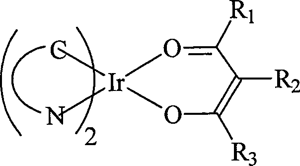
Priority Applications (7)
| Application Number | Priority Date | Filing Date | Title |
|---|---|---|---|
| DE102010054893A DE102010054893A1 (en) | 2010-12-17 | 2010-12-17 | Radiation-emitting organic-electronic device and method for its production |
| US13/994,953 US9735397B2 (en) | 2010-12-17 | 2011-12-13 | Radiation-emitting organic-electronic device and method for the production thereof |
| JP2013543723A JP6008869B2 (en) | 2010-12-17 | 2011-12-13 | LIGHT EMITTING ORGANIC ELECTRONIC DEVICE AND METHOD FOR MANUFACTURING THE SAME |
| CN201180060825.7A CN103262286B (en) | 2010-12-17 | 2011-12-13 | Radiation-emitting organic electronic device and method of manufacturing the same |
| PCT/EP2011/072632 WO2012080267A2 (en) | 2010-12-17 | 2011-12-13 | Radiation-emitting organic-electronic device and method for the production thereof |
| EP11794750.7A EP2652810B9 (en) | 2010-12-17 | 2011-12-13 | Method of forming a radiation-emitting organic-electronic device |
| KR1020137018620A KR101930411B1 (en) | 2010-12-17 | 2011-12-13 | Radiation-emitting organic-electronic device and method for the production thereof |
Applications Claiming Priority (1)
| Application Number | Priority Date | Filing Date | Title |
|---|---|---|---|
| DE102010054893A DE102010054893A1 (en) | 2010-12-17 | 2010-12-17 | Radiation-emitting organic-electronic device and method for its production |
Publications (1)
| Publication Number | Publication Date |
|---|---|
| DE102010054893A1 true DE102010054893A1 (en) | 2012-06-21 |
Family
ID=45346485
Family Applications (1)
| Application Number | Title | Priority Date | Filing Date |
|---|---|---|---|
| DE102010054893A Withdrawn DE102010054893A1 (en) | 2010-12-17 | 2010-12-17 | Radiation-emitting organic-electronic device and method for its production |
Country Status (7)
| Country | Link |
|---|---|
| US (1) | US9735397B2 (en) |
| EP (1) | EP2652810B9 (en) |
| JP (1) | JP6008869B2 (en) |
| KR (1) | KR101930411B1 (en) |
| CN (1) | CN103262286B (en) |
| DE (1) | DE102010054893A1 (en) |
| WO (1) | WO2012080267A2 (en) |
Cited By (4)
| Publication number | Priority date | Publication date | Assignee | Title |
|---|---|---|---|---|
| DE102011086255A1 (en) * | 2011-11-14 | 2013-05-16 | Osram Opto Semiconductors Gmbh | ORGANIC LIGHT EMITTING COMPONENT |
| DE102012200180A1 (en) * | 2012-01-09 | 2013-07-11 | Osram Opto Semiconductors Gmbh | Method for producing optoelectronic organic components, device therefor and optoelectronic organic component |
| DE102012203583A1 (en) * | 2012-03-07 | 2013-09-12 | Osram Opto Semiconductors Gmbh | Organic light emitting device |
| DE102013113533A1 (en) * | 2013-12-05 | 2015-06-11 | Osram Oled Gmbh | Conversion element and method for producing a conversion element |
Families Citing this family (29)
| Publication number | Priority date | Publication date | Assignee | Title |
|---|---|---|---|---|
| WO2014047616A1 (en) | 2012-09-24 | 2014-03-27 | Arizona Board Of Regents For And On Behalf Of Arizona State University | Metal compounds, methods, and uses thereof |
| WO2014109814A2 (en) | 2012-10-26 | 2014-07-17 | Arizona Board Of Regents Acting For And On Behalf Of Arizona State University | Metal complexes, methods, and uses thereof |
| JP6804823B2 (en) | 2013-10-14 | 2020-12-23 | アリゾナ・ボード・オブ・リージェンツ・オン・ビハーフ・オブ・アリゾナ・ステイト・ユニバーシティーArizona Board of Regents on behalf of Arizona State University | Platinum complex and device |
| US10020455B2 (en) | 2014-01-07 | 2018-07-10 | Arizona Board Of Regents On Behalf Of Arizona State University | Tetradentate platinum and palladium complex emitters containing phenyl-pyrazole and its analogues |
| JP2015201315A (en) * | 2014-04-07 | 2015-11-12 | 株式会社ジャパンディスプレイ | Organic EL display device |
| DE102014107106A1 (en) * | 2014-05-20 | 2015-11-26 | Von Ardenne Gmbh | Method for producing a layer with semicrystalline regions and method for producing a thin-film component |
| US9941479B2 (en) | 2014-06-02 | 2018-04-10 | Arizona Board Of Regents On Behalf Of Arizona State University | Tetradentate cyclometalated platinum complexes containing 9,10-dihydroacridine and its analogues |
| US9923155B2 (en) | 2014-07-24 | 2018-03-20 | Arizona Board Of Regents On Behalf Of Arizona State University | Tetradentate platinum (II) complexes cyclometalated with functionalized phenyl carbene ligands and their analogues |
| US10793546B2 (en) | 2014-08-15 | 2020-10-06 | Arizona Board Of Regents On Behalf Of Arizona State University | Non-platinum metal complexes for excimer based single dopant white organic light emitting diodes |
| US11329244B2 (en) | 2014-08-22 | 2022-05-10 | Arizona Board Of Regents On Behalf Of Arizona State University | Organic light-emitting diodes with fluorescent and phosphorescent emitters |
| US10033003B2 (en) | 2014-11-10 | 2018-07-24 | Arizona Board Of Regents On Behalf Of Arizona State University | Tetradentate metal complexes with carbon group bridging ligands |
| US9879039B2 (en) | 2015-06-03 | 2018-01-30 | Arizona Board Of Regents On Behalf Of Arizona State University | Tetradentate and octahedral metal complexes containing naphthyridinocarbazole and its analogues |
| US10672996B2 (en) * | 2015-09-03 | 2020-06-02 | Universal Display Corporation | Organic electroluminescent materials and devices |
| US11335865B2 (en) | 2016-04-15 | 2022-05-17 | Arizona Board Of Regents On Behalf Of Arizona State University | OLED with multi-emissive material layer |
| US10822363B2 (en) | 2016-10-12 | 2020-11-03 | Arizona Board Of Regents On Behalf Of Arizona State University | Narrow band red phosphorescent tetradentate platinum (II) complexes |
| US11183670B2 (en) | 2016-12-16 | 2021-11-23 | Arizona Board Of Regents On Behalf Of Arizona State University | Organic light emitting diode with split emissive layer |
| WO2018140765A1 (en) | 2017-01-27 | 2018-08-02 | Jian Li | Metal-assisted delayed fluorescent emitters employing pyrido-pyrrolo-acridine and analogues |
| US10516117B2 (en) | 2017-05-19 | 2019-12-24 | Arizona Board Of Regents On Behalf Of Arizona State University | Metal-assisted delayed fluorescent emttters employing benzo-imidazo-phenanthridine and analogues |
| US11101435B2 (en) | 2017-05-19 | 2021-08-24 | Arizona Board Of Regents On Behalf Of Arizona State University | Tetradentate platinum and palladium complexes based on biscarbazole and analogues |
| US11647643B2 (en) | 2017-10-17 | 2023-05-09 | Arizona Board Of Regents On Behalf Of Arizona State University | Hole-blocking materials for organic light emitting diodes |
| KR102718677B1 (en) * | 2017-10-17 | 2024-10-16 | 지안 리 | Phosphorescent excimers with desirable molecular orientation as monochromatic emitters for display and lighting applications |
| CN111801985B (en) * | 2018-02-28 | 2022-09-27 | Sabic环球技术有限责任公司 | Method and apparatus for emitting radiation or heat from a surface |
| US12037348B2 (en) | 2018-03-09 | 2024-07-16 | Arizona Board Of Regents On Behalf Of Arizona State University | Blue and narrow band green and red emitting metal complexes |
| US11878988B2 (en) | 2019-01-24 | 2024-01-23 | Arizona Board Of Regents On Behalf Of Arizona State University | Blue phosphorescent emitters employing functionalized imidazophenthridine and analogues |
| US11594691B2 (en) | 2019-01-25 | 2023-02-28 | Arizona Board Of Regents On Behalf Of Arizona State University | Light outcoupling efficiency of phosphorescent OLEDs by mixing horizontally aligned fluorescent emitters |
| US11785838B2 (en) | 2019-10-02 | 2023-10-10 | Arizona Board Of Regents On Behalf Of Arizona State University | Green and red organic light-emitting diodes employing excimer emitters |
| US11945985B2 (en) | 2020-05-19 | 2024-04-02 | Arizona Board Of Regents On Behalf Of Arizona State University | Metal assisted delayed fluorescent emitters for organic light-emitting diodes |
| CN113683625B (en) | 2020-05-19 | 2025-06-10 | 亚利桑那州立大学董事会 | Metal-assisted delayed fluorescence emitters for organic light emitting diodes |
| EP3937268B1 (en) * | 2020-07-10 | 2025-05-07 | Universal Display Corporation | Plasmonic oleds and vertical dipole emitters |
Citations (4)
| Publication number | Priority date | Publication date | Assignee | Title |
|---|---|---|---|---|
| DE10311767A1 (en) * | 2003-03-18 | 2004-09-30 | H.C. Starck Gmbh | Conjugated phosphorescent and luminescent polymers containing covalently-bonded metal complexes, useful as emitters in light-emitting systems such as diodes and displays |
| US20050087131A1 (en) * | 2003-10-23 | 2005-04-28 | Max Shtein | Method and apparatus for depositing material |
| EP1486552B1 (en) * | 2003-06-12 | 2007-12-19 | Sony Corporation | Organic electroluminescent material, organic electroluminescent device, and heterocycle-containing iridium complex compound |
| WO2010112799A1 (en) * | 2009-02-26 | 2010-10-07 | University Of York | Luminophores comprising platinum-ligand complexes |
Family Cites Families (13)
| Publication number | Priority date | Publication date | Assignee | Title |
|---|---|---|---|---|
| JP4589346B2 (en) * | 1999-07-14 | 2010-12-01 | 三星モバイルディスプレイ株式會社 | Organic electroluminescence device and panel manufacturing method and manufacturing apparatus |
| TW518908B (en) | 1999-07-14 | 2003-01-21 | Nec Corp | Organic electroluminescent element, and method for manufacturing the same |
| JP3965319B2 (en) * | 2001-03-08 | 2007-08-29 | ザ ユニヴァーシティ オブ ホンコン | Organometallic light emitting material |
| DE10330761A1 (en) * | 2003-07-07 | 2005-02-03 | Covion Organic Semiconductors Gmbh | New organometallic compounds are useful for the production of electronic components, organic light emitting diodes, organic integrated circuits and organic field effect transistors |
| JP2006085933A (en) | 2004-09-14 | 2006-03-30 | Toshiba Matsushita Display Technology Co Ltd | Display device manufacturing method and manufacturing apparatus |
| US7923128B2 (en) * | 2005-06-07 | 2011-04-12 | Fujifilm Corporation | Organic electroluminescent device |
| JP2007114244A (en) * | 2005-10-18 | 2007-05-10 | Jsr Corp | Radiation sensitive resin composition and formation of interlayer insulating film and microlens |
| KR20080085000A (en) | 2005-12-01 | 2008-09-22 | 신닛테츠가가쿠 가부시키가이샤 | Organic electroluminescent device |
| EP2001065B1 (en) * | 2006-03-30 | 2016-11-09 | Konica Minolta Holdings, Inc. | Organic electroluminescent device, illuminating device and display device |
| US20070247061A1 (en) * | 2006-04-20 | 2007-10-25 | Vadim Adamovich | Multiple dopant emissive layer OLEDs |
| US7282586B1 (en) * | 2006-08-11 | 2007-10-16 | Luminescence Technology Corp. | Dipyridine-based compound and the use thereof |
| JP2009211892A (en) * | 2008-03-03 | 2009-09-17 | Fujifilm Corp | Organic electroluminescent element |
| JP4853506B2 (en) * | 2008-10-09 | 2012-01-11 | コニカミノルタホールディングス株式会社 | White light emitting organic electroluminescence device |
-
2010
- 2010-12-17 DE DE102010054893A patent/DE102010054893A1/en not_active Withdrawn
-
2011
- 2011-12-13 EP EP11794750.7A patent/EP2652810B9/en active Active
- 2011-12-13 WO PCT/EP2011/072632 patent/WO2012080267A2/en not_active Ceased
- 2011-12-13 JP JP2013543723A patent/JP6008869B2/en not_active Expired - Fee Related
- 2011-12-13 CN CN201180060825.7A patent/CN103262286B/en not_active Expired - Fee Related
- 2011-12-13 KR KR1020137018620A patent/KR101930411B1/en not_active Expired - Fee Related
- 2011-12-13 US US13/994,953 patent/US9735397B2/en not_active Expired - Fee Related
Patent Citations (4)
| Publication number | Priority date | Publication date | Assignee | Title |
|---|---|---|---|---|
| DE10311767A1 (en) * | 2003-03-18 | 2004-09-30 | H.C. Starck Gmbh | Conjugated phosphorescent and luminescent polymers containing covalently-bonded metal complexes, useful as emitters in light-emitting systems such as diodes and displays |
| EP1486552B1 (en) * | 2003-06-12 | 2007-12-19 | Sony Corporation | Organic electroluminescent material, organic electroluminescent device, and heterocycle-containing iridium complex compound |
| US20050087131A1 (en) * | 2003-10-23 | 2005-04-28 | Max Shtein | Method and apparatus for depositing material |
| WO2010112799A1 (en) * | 2009-02-26 | 2010-10-07 | University Of York | Luminophores comprising platinum-ligand complexes |
Non-Patent Citations (2)
| Title |
|---|
| Danz et al. J. Opt. Soc. Am. B/Vol. 19, No. 3, 412-419 |
| Krummacher et al., Organic Electronics 10 (2009) 478-485 |
Cited By (7)
| Publication number | Priority date | Publication date | Assignee | Title |
|---|---|---|---|---|
| DE102011086255A1 (en) * | 2011-11-14 | 2013-05-16 | Osram Opto Semiconductors Gmbh | ORGANIC LIGHT EMITTING COMPONENT |
| US9293733B2 (en) | 2011-11-14 | 2016-03-22 | Osram Oled Gmbh | Organic light-emitting component having a layer with a low absorption coefficient |
| DE102012200180A1 (en) * | 2012-01-09 | 2013-07-11 | Osram Opto Semiconductors Gmbh | Method for producing optoelectronic organic components, device therefor and optoelectronic organic component |
| DE102012203583A1 (en) * | 2012-03-07 | 2013-09-12 | Osram Opto Semiconductors Gmbh | Organic light emitting device |
| US10454050B2 (en) | 2012-03-07 | 2019-10-22 | Osram Oled Gmbh | Organic light-emitting device |
| DE102012203583B4 (en) * | 2012-03-07 | 2021-03-18 | Pictiva Displays International Limited | Organic light-emitting component |
| DE102013113533A1 (en) * | 2013-12-05 | 2015-06-11 | Osram Oled Gmbh | Conversion element and method for producing a conversion element |
Also Published As
| Publication number | Publication date |
|---|---|
| EP2652810A2 (en) | 2013-10-23 |
| US9735397B2 (en) | 2017-08-15 |
| US20140014931A1 (en) | 2014-01-16 |
| JP2014504430A (en) | 2014-02-20 |
| WO2012080267A2 (en) | 2012-06-21 |
| WO2012080267A3 (en) | 2012-08-16 |
| KR101930411B1 (en) | 2018-12-18 |
| EP2652810B9 (en) | 2021-11-10 |
| CN103262286A (en) | 2013-08-21 |
| JP6008869B2 (en) | 2016-10-19 |
| CN103262286B (en) | 2016-02-03 |
| KR20130107343A (en) | 2013-10-01 |
| EP2652810B1 (en) | 2021-08-11 |
Similar Documents
| Publication | Publication Date | Title |
|---|---|---|
| EP2652810B9 (en) | Method of forming a radiation-emitting organic-electronic device | |
| DE112012007317B4 (en) | Light-emitting element, electronic equipment and lighting equipment | |
| DE602004005014T2 (en) | ORGANIC LIGHT-EMITTING COMPONENTS USING BINUCLEAR METAL COMPOSITIONS AS EMISSION MATERIALS | |
| DE69729931T2 (en) | ORGANIC ELECTROLIMIC CENTER DEVICE | |
| DE102013109451B9 (en) | Method for producing an optoelectronic component | |
| DE102011086277B4 (en) | Organic light-emitting device | |
| EP2483945B1 (en) | Organic electronic device and method for the production thereof | |
| EP2335301B1 (en) | Radiation emitting device | |
| DE102009041289A1 (en) | Organic electroluminescent device | |
| EP2253032B1 (en) | Optoelectronic component comprising neutral transition metal complexes | |
| EP2652809B1 (en) | Organic light emitting device and use of a copper complex in a charge transfer layer | |
| EP2588563A2 (en) | Singlet harvesting with organic molecules for optoelectronic devices | |
| DE102011089687A1 (en) | Singlet Harvesting with special organic molecules without metal centers for opto-electronic devices | |
| DE102011007052A1 (en) | Optoelectronic component and use of a copper complex as a dopant for doping a layer | |
| DE102012203583A1 (en) | Organic light emitting device | |
| DE102012207151A1 (en) | ORGANIC LIGHT-EMITTING COMPONENT AND METHOD FOR PRODUCING AN ORGANIC LIGHT-EMITTING COMPONENT | |
| DE102007023876A1 (en) | Electric organic component comprises substrate, former electrode, which has anode, former electrically semiconducting layer on former electrode, organic functional layer on former electrically semiconducting layer | |
| DE112006000495T5 (en) | Multilayer light emitting polymer diode for solid state lighting applications | |
| DE102013103156B4 (en) | A radiation-emitting organic-electronic device and method for producing a radiation-emitting organic-electronic device | |
| WO2015140110A1 (en) | Organic optoelectronic apparatus | |
| WO2013104571A1 (en) | Method for producing optoelectronic organic components, device therefor and optoelectronic organic component | |
| WO2017085078A1 (en) | Organic electronic component, use of a p-type dopant for a matrix material | |
| DE112020002335T5 (en) | Light-emitting device, light-emitting device, light-emitting module, electronic device, and lighting device | |
| DE102007061755A1 (en) | Component for phosphorescent light emission from triplet states and method for producing such devices |
Legal Events
| Date | Code | Title | Description |
|---|---|---|---|
| R163 | Identified publications notified | ||
| R081 | Change of applicant/patentee |
Owner name: FRAUNHOFER-GESELLSCHAFT ZUR FOERDERUNG DER ANG, DE Free format text: FORMER OWNERS: OSRAM OPTO SEMICONDUCTORS GESELLSCHAFT MIT BESCHRAENKTER HAFTUNG, 93055 REGENSBURG, DE; FRAUNHOFER-GESELLSCHAFT ZUR FOERDERUNG DER ANGEWANDTEN FORSCHUNG E.V., 80686 MUENCHEN, DE Owner name: OSRAM OLED GMBH, DE Free format text: FORMER OWNERS: OSRAM OPTO SEMICONDUCTORS GESELLSCHAFT MIT BESCHRAENKTER HAFTUNG, 93055 REGENSBURG, DE; FRAUNHOFER-GESELLSCHAFT ZUR FOERDERUNG DER ANGEWANDTEN FORSCHUNG E.V., 80686 MUENCHEN, DE Owner name: FRAUNHOFER-GESELLSCHAFT ZUR FOERDERUNG DER ANG, DE Free format text: FORMER OWNERS: OSRAM OPTO SEMICONDUCTORS GMBH, 93055 REGENSBURG, DE; FRAUNHOFER-GESELLSCHAFT ZUR FOERDERUNG DER ANGEWANDTEN FORSCHUNG E.V., 80686 MUENCHEN, DE Owner name: OSRAM OLED GMBH, DE Free format text: FORMER OWNERS: OSRAM OPTO SEMICONDUCTORS GMBH, 93055 REGENSBURG, DE; FRAUNHOFER-GESELLSCHAFT ZUR FOERDERUNG DER ANGEWANDTEN FORSCHUNG E.V., 80686 MUENCHEN, DE |
|
| R082 | Change of representative |
Representative=s name: EPPING HERMANN FISCHER, PATENTANWALTSGESELLSCH, DE Representative=s name: EPPING HERMANN FISCHER PATENTANWALTSGESELLSCHA, DE |
|
| R005 | Application deemed withdrawn due to failure to request examination |