DE102006059411A1 - Method for producing optical sensor for mounting on carrier substrate, involves providing optical transparent plate with lateral dimensions larger than sensor chip - Google Patents
Method for producing optical sensor for mounting on carrier substrate, involves providing optical transparent plate with lateral dimensions larger than sensor chip Download PDFInfo
- Publication number
- DE102006059411A1 DE102006059411A1 DE102006059411A DE102006059411A DE102006059411A1 DE 102006059411 A1 DE102006059411 A1 DE 102006059411A1 DE 102006059411 A DE102006059411 A DE 102006059411A DE 102006059411 A DE102006059411 A DE 102006059411A DE 102006059411 A1 DE102006059411 A1 DE 102006059411A1
- Authority
- DE
- Germany
- Prior art keywords
- electrical connection
- connection elements
- sensor chip
- transparent plate
- carrier substrate
- Prior art date
- Legal status (The legal status is an assumption and is not a legal conclusion. Google has not performed a legal analysis and makes no representation as to the accuracy of the status listed.)
- Ceased
Links
Classifications
-
- H—ELECTRICITY
- H10—SEMICONDUCTOR DEVICES; ELECTRIC SOLID-STATE DEVICES NOT OTHERWISE PROVIDED FOR
- H10F—INORGANIC SEMICONDUCTOR DEVICES SENSITIVE TO INFRARED RADIATION, LIGHT, ELECTROMAGNETIC RADIATION OF SHORTER WAVELENGTH OR CORPUSCULAR RADIATION
- H10F77/00—Constructional details of devices covered by this subclass
- H10F77/50—Encapsulations or containers
-
- H—ELECTRICITY
- H04—ELECTRIC COMMUNICATION TECHNIQUE
- H04N—PICTORIAL COMMUNICATION, e.g. TELEVISION
- H04N23/00—Cameras or camera modules comprising electronic image sensors; Control thereof
- H04N23/50—Constructional details
- H04N23/54—Mounting of pick-up tubes, electronic image sensors, deviation or focusing coils
-
- H—ELECTRICITY
- H04—ELECTRIC COMMUNICATION TECHNIQUE
- H04N—PICTORIAL COMMUNICATION, e.g. TELEVISION
- H04N23/00—Cameras or camera modules comprising electronic image sensors; Control thereof
- H04N23/57—Mechanical or electrical details of cameras or camera modules specially adapted for being embedded in other devices
-
- H—ELECTRICITY
- H10—SEMICONDUCTOR DEVICES; ELECTRIC SOLID-STATE DEVICES NOT OTHERWISE PROVIDED FOR
- H10F—INORGANIC SEMICONDUCTOR DEVICES SENSITIVE TO INFRARED RADIATION, LIGHT, ELECTROMAGNETIC RADIATION OF SHORTER WAVELENGTH OR CORPUSCULAR RADIATION
- H10F39/00—Integrated devices, or assemblies of multiple devices, comprising at least one element covered by group H10F30/00, e.g. radiation detectors comprising photodiode arrays
- H10F39/80—Constructional details of image sensors
- H10F39/804—Containers or encapsulations
-
- H10W90/754—
Landscapes
- Engineering & Computer Science (AREA)
- Multimedia (AREA)
- Signal Processing (AREA)
- Solid State Image Pick-Up Elements (AREA)
- Transforming Light Signals Into Electric Signals (AREA)
Abstract
Die vorliegende Erfindung betrifft einen optischen Sensor, der einen optischen Sensorchip mit einer optisch sensitiven Fläche und einer darüber angeordneten optisch transparenten Platte umfasst, sowie ein Verfahren zu dessen Herstellung. Bei dem Verfahren wird auf eine Rückseite der optisch transparenten Platte eine Leiterbahnstruktur mit ersten und zweiten elektrischen Anschlusselementen und Leiterbahnen aufgebracht, über die der Sensorchip nach Fertigstellung des optischen Sensors elektrisch kontaktierbar ist. Die Rückseite der optisch transparenten Platte wird mittels eines anisotrop elektrisch leitenden Klebstoffs direkt mit dem Sensorchip verbunden, wobei die ersten elektrischen Anschlusselemente der optisch transparenten Platte über elektrischen Anschlusselementen des Sensorchips liegen. Der Klebstoff wird dabei derart aufgebracht, dass eine elektrische Verbindung zwischen den ersten elektrischen Anschlusselementen und den elektrischen Anschlusselementen des Sensorchips hergestellt und die optisch sensitive Fläche des Sensorchips nicht vom Klebstoff abgeschattet wird. Mit dem Verfahren wird ein optischer Sensor erhalten, der eine geringe Bauhöhe aufweist und auf einfache Weise auf einem Trägersubstrat, bspw. einer Leiterplatte, montiert werden kann.The The present invention relates to an optical sensor comprising a optical sensor chip with an optically sensitive surface and one about it arranged optically transparent plate comprises, as well as a method for its production. In the process is on a back the optically transparent plate, a conductor track structure with first and second electrical connection elements and printed conductors, via which the Sensor chip after completion of the optical sensor electrical is contactable. The backside the optically transparent plate is electrically anisotropic by means of an anisotropic conductive adhesive directly connected to the sensor chip, wherein the first electrical connection elements of the optically transparent Plate over electrical connection elements of the sensor chip lie. The adhesive is applied in such a way that an electrical connection between the first electrical connection elements and the electrical Connection elements of the sensor chip produced and the optically sensitive area of the sensor chip is not shaded by the adhesive. With the procedure an optical sensor is obtained which has a low overall height and in a simple manner on a carrier substrate, for example a printed circuit board, can be mounted.
Description
Technisches AnwendungsgebietTechnical application
Die vorliegende Erfindung betrifft einen optischen Sensor für die Montage auf einem Trägersubstrat, der einen optischen Sensorchip mit einer optisch sensitiven Fläche und einer darüber angeordneten optisch transparenten Platte umfasst. Die Erfindung betrifft auch ein Verfahren zur Herstellung eines derartigen optischen Sensors für die Montage auf einem Trägersubstrat.The The present invention relates to an optical sensor for mounting on a carrier substrate, the one optical sensor chip with an optically sensitive surface and one about it arranged optically transparent plate comprises. The invention also relates to a method for producing such an optical Sensors for the mounting on a carrier substrate.
Optische Sensoren werden heutzutage für viele Anwendungsbereiche benötigt, bspw. in fotographischen Kameras, in Mobiltelefonen oder in der Medizintechnik. Die zunehmende Miniaturisierung erfordert auch bei optischen Sensoren eine möglichst kompakte Bauweise.optical Sensors are nowadays for many Application areas needed, for example in photographic cameras, in mobile phones or in medical technology. The increasing miniaturization also requires optical sensors a compact as possible Construction.
Im Grundaufbau umfasst ein optischer Sensor einen optischen Sensorchip und eine über dem Sensorchip angeordnete optisch transparente Platte. Die optisch transparente Platte, in der Regel aus einem optischen Glas, dient dem Schutz der optisch sensitiven Fläche des Sensorchips und kann durch geeignete Ausgestaltung auch als Filter dienen. Gerade im Bereich der optischen Fotographie ist der Einsatz eines Infrarot(IR)-Filters vor dem optischen Sensor erforderlich, um Farbverschiebungen Bild zu vermeiden.in the Basic construction includes an optical sensor, an optical sensor chip and one over the sensor chip arranged optically transparent plate. The optical transparent plate, usually made of an optical glass, is used the protection of the optically sensitive surface of the sensor chip and can by suitable design also serve as a filter. Especially in the The field of optical photography is the use of an infrared (IR) filter in front of the optical sensor required to image color shifts to avoid.
Bei der Montage für die jeweilige Anwendung wird der optische Sensor auf ein Trägersubstrat mit den entsprechenden elektrischen Zuführungen und Kontakten, in der Regel eine Leiterplatte, montiert und anschließend durch geeignete Verkapselung gegen Umwelteinflüsse, insbesondere Feuchte, abgedichtet. In vielen Fällen wird ein Gehäuse eingesetzt, das an der Lichteintrittsseite oberhalb der optisch transparenten Platte auch eine Halterung für eine Linse aufweist, die der optischen Abbildung auf die optisch sensitive Fläche des Sensorchips dient.at the assembly for the particular application is the optical sensor on a carrier substrate with the corresponding electrical leads and contacts, in the Usually a circuit board, mounted and then by suitable encapsulation against environmental influences, in particular moisture, sealed. In many cases, a housing is used that at the light entrance side above the optically transparent plate also a holder for has a lens that the optical image on the optical sensitive area of the sensor chip is used.
Stand der TechnikState of the art
Bei
der Montage wird die mechanische Verbindung zwischen dem Sensorchip
und dem Trägersubstrat
durch Löt-
oder Klebetechniken realisiert. Die elektrische Verbindung zwischen
den auf dem Sensorchip um die optisch sensitive Fläche herum angeordneten
elektrischen Anschlussflächen
und korrespondierenden Anschlussflächen auf dem Trägersubstrat
erfolgt bisher in der Regel im Drahtbondverfahren.
Aus
einer Veröffentlichung
der Firma Schott (
Die Aufgabe der vorliegenden Erfindung besteht darin, einen optischen Sensor für die Montage auf einem Trägersubstrat sowie ein Verfahren zur Herstellung anzugeben, die eine kostengünstige Herstellung des optischen Sensors bei flacher Bauweise ermöglichen.The Object of the present invention is to provide an optical Sensor for the mounting on a carrier substrate and to provide a method of production which is a cost effective production allow the optical sensor in a flat design.
Darstellung der ErfindungPresentation of the invention
Die Aufgabe wird mit dem Verfahren und dem optischen Sensor gemäß den Patentansprüchen 1 und 14 gelöst. Vorteilhafte Ausgestaltungen des Verfahrens sowie des optischen Sensors sind Gegenstand der Unteransprüche oder lassen sich der nachfolgenden Beschreibung sowie dem Ausführungsbeispiel entnehmen.The Task is with the method and the optical sensor according to claims 1 and 14 solved. Advantageous embodiments of the method and the optical Sensors are the subject of the dependent claims or can be the following Description and the embodiment remove.
Bei dem vorgeschlagenen Verfahren wird eine optisch transparente Platte bereitgestellt, auf die erste und zweite elektrische Anschlusselemente und Leiterbahnen auf eine dem Sensorchip zugewandte Rückseite aufgebracht werden, über die der Sensorchip nach Fertigstellung des optischen Sensors elektrisch kontaktierbar ist. Bei den ersten elektrischen Anschlusselementen handelt es sich vorzugsweise um Anschlussflächen (Anschlusspads), die zweiten elektrischen Anschlusselemente können entweder als Anschlussflächen oder als Anschlusskörper, bspw. als Lothöcker oder Lotbumps, realisiert sein. Die lateralen Abmessungen (d. h. Länge und/oder Breite) der optisch transparenten Platte, die vorzugsweise aus einem optischen Glas besteht, werden größer gewählt als die lateralen Abmessungen des Sensorchips. Damit ergibt sich ein erster Bereich der optisch transparenten Platte, der über dem Sensorchip liegt, und ein zweiter Bereich, der über den Sensorchip hinausragt. Unter dem zweiten Bereich können in der vorliegenden Patentanmeldung auch mehrere nicht zusammenhängende Teilbereiche verstanden werden.In the proposed method, an optically transparent plate is provided, to which first and second electrical connection elements and conductor tracks are applied to a rear side facing the sensor chip, via which the sensor chip can be electrically contacted after completion of the optical sensor. The first electrical connection elements are preferably connection surfaces (connection pads), the second electrical connection elements can be realized either as connection surfaces or as connection bodies, for example as solder bumps or solder bumps. The lateral dimensions (ie length and / or width) of the optically transparent plate, which preferably consists of an optical glass, are chosen larger than the lateral dimensions of the sensor chip. This results in a first range of optically transparent plate that overlies the sensor chip and a second region that extends beyond the sensor chip. In the present patent application, the second area can also be understood as meaning several non-contiguous subareas.
Die ersten Anschlusselemente werden korrespondierend zu Anschlusselementen des Sensorchips im ersten Bereich erzeugt, so dass sie bei der späteren Verbindung der Platte mit dem Sensorchip direkt über den Anschlusselementen des Sensorchips liegen, während die zweiten elektrischen Anschlusselemente im zweiten Bereich erzeugt werden. Die ersten und zweiten elektrischen Anschlusselemente werden über die Leiterbahnen elektrisch miteinander verbunden. Das Aufbringen dieser Anschlusselemente und Leiterbahnen auf die Rückseite der optisch transparenten Platte kann über Verfahren erfolgen, wie sie aus der Display-Technik bekannt sind, bspw. durch eine Metall-Sputter-Technik oder durch Siebdruck.The first connection elements are corresponding to connection elements of the sensor chip generated in the first area, allowing them to connect later the plate with the sensor chip directly over the connection elements of the sensor chip while generates the second electrical connection elements in the second area become. The first and second electrical connection elements are over the Conductors electrically connected. The application of this Connection elements and conductor tracks on the back of the optically transparent Plate can over Method, as they are known from the display technology, for example. By a Metal sputtering technique or by screen printing.
Als Material für die Anschlusselemente und Leiterbahnen kann ein optisch transparentes, elektrisch leitfähiges Material eingesetzt werden, vorzugsweise ITO (Indiumzinnoxid). In diesem Falle können die Leiterbahnen auch quer durch den ersten Bereich verlaufen, da sie die optisch sensitive Fläche des Sensorchips nicht abschatten. Werden für die Aufbringung der Anschlusselemente und Leiterbahnen andere Materialien eingesetzt, bspw. Aluminium, Gold oder Kupfer, so wird das Design bzw. der Verlauf der Leiterbahnen so gewählt, dass sie die optisch sensitive Fläche des Sensorchips nicht abschatten.When Material for the connection elements and conductor tracks can be an optically transparent, electrically conductive Material can be used, preferably ITO (indium tin oxide). In this case can the tracks also run across the first area, since they are the optically sensitive surface of the Do not shade the sensor chips. Be used for the application of the connection elements and conductors other materials used, for example. Aluminum, gold or copper, this is the design or the course of the tracks chosen so that they do not shade the optically sensitive surface of the sensor chip.
Anschließend wird die Rückseite der optisch transparenten Platte mittels eines anisotrop elektrisch leitenden Klebstoffs (auch unter dem Begriff anisotroper Kleber bekannt) direkt mit dem Sensorchip verbunden, wobei die ersten elektrischen Anschlusselemente der optisch transparenten Platte über den elektrischen Anschlusselementen des Sensorchips liegen. Der Klebstoff wird dabei derart vorzugsweise strukturiert aufgebracht, dass eine elektrische Verbindung zwischen den ersten elektrischen Anschlusselementen der optisch transparenten Platte und den elektrischen Anschlusselementen des Sensorchips hergestellt und die optisch sensitive Fläche des Sensorchips nicht vom Klebstoff abgeschattet wird. Der Auftrag des Klebers kann dabei bspw. mit einem Dispenser erfolgen. Für die Herstellung der Verbindung muss der Kleber zumindest an Stellen aufgebracht werden, an denen die elektrischen Anschlusselemente von Sensorchip und Platte elektrisch miteinander verbunden werden sollen. Bei einem optisch nicht transparenten Klebstoff wird auf die optisch sensitive Fläche kein Klebstoff aufgebracht, um diese Fläche nicht abzuschatten. Bei Einsatz eines optisch transparenten Klebstoffs kann auch auf diese strukturierte Aufbringung verzichtet werden. Der Klebstoff kann dann auch vollflächig aufgebracht werden.Subsequently, will the backside the optically transparent plate by means of an anisotropic electric conductive adhesive (also under the term anisotropic adhesive known) directly connected to the sensor chip, wherein the first electrical Connection elements of the optically transparent plate over the electrical connection elements of the sensor chip lie. The adhesive is preferably applied structured so that a electrical connection between the first electrical connection elements the optically transparent plate and the electrical connection elements made of the sensor chip and the optically sensitive surface of the Sensor chips are not shaded by the adhesive. The order of the Adhesives can be done, for example, with a dispenser. For the production the compound must be at least applied in places the adhesive are where the electrical connection elements of sensor chip and plate to be electrically connected to each other. At a optically non-transparent adhesive is applied to the optically sensitive area no glue applied to avoid shading this area. at Use of an optically transparent adhesive can also be applied to this structured application can be dispensed with. The glue can then also over the entire surface be applied.
Auf diese Weise wird ein kostengünstig herstellbarer optischer Sensor erhalten, der eine sehr flache Bauweise aufweist und über die zweiten Anschlusselemente auf der Rückseite der optisch transparenten Platte (im zweiten Bereich) auf einfache Weise elektrisch kontaktiert werden kann.On This way will be a cost effective obtainable optical sensor, which has a very flat design and over the second connection elements on the back of the optically transparent Plate (in the second area) contacted in a simple manner electrically can be.
Der mit dem Verfahren herstellbare optische Sensor umfasst dementsprechend einen optischen Sensorchip mit einer optisch sensitiven Fläche und eine darüber angeordnete optisch transparente Platte, wobei die optisch transparente Platte einen über dem Sensorchip liegenden ersten Bereich und einen seitlich über den Sensorchip hinausragenden zweiten Bereich aufweist. Auf der dem Sensorchip zugewandten Rückseite sind im ersten Bereich die ersten elektrischen Anschlusselemente über korrespondierenden elektrischen Anschlusselementen des Sensorchips und im zweiten Bereich zweite elektrische Anschlusselemente angeordnet, wobei jeweils erste und zweite elektrische Anschlusselemente, vorzugsweise jeweils ein erstes mit einem zweiten Anschlusselement, über Leiterbahnen auf der Rückseite der optisch transparenten Platte miteinander verbunden sind. Die optisch transparente Platte ist mit ihrer Rückseite über einen anisotrop elektrisch leitenden Klebstoff so mit dem Sensorchip verbunden, dass eine elektrische Verbindung zwischen den elektrischen Anschlusselementen des Sensorchips und den jeweils an gleicher Position darüber liegenden ersten elektrischen Anschlusselementen der optisch transparenten Platte besteht und die optisch sensitive Fläche des Sensorchips nicht vom Klebstoff abgeschattet wird.Of the The optical sensor that can be produced by the method accordingly an optical sensor chip with an optically sensitive surface and a about that arranged optically transparent plate, wherein the optically transparent Plate one above the Sensor chip lying first area and one side over the Sensor chip protruding second region. On the Sensor chip facing back In the first area, the first electrical connection elements are via corresponding ones electrical connection elements of the sensor chip and in the second area second electrical connection elements arranged, wherein each first and second electrical connection elements, preferably in each case a first with a second connection element, via conductor tracks on the back the optically transparent plate are interconnected. The Optically transparent plate is electrically anisotropic with its backside over an anisotropic conductive adhesive so connected to the sensor chip that an electric Connection between the electrical connection elements of the sensor chip and in each case at the same position overlying first electrical Connection elements of the optically transparent plate consists and the optically sensitive surface of the sensor chip is not shaded by the adhesive.
Bei der Montage eines derart aufgebauten optischen Sensors wird ein Trägersubstrat bereitgestellt, auf dem elektrische Anschlusselemente und Leiterbahnen für den optischen Sensor vorgesehen sind. Die elektrischen Anschlusselemente sind hierbei so angeordnet, dass sie bei Aufsetzen des optischen Sensors direkt unter den zweiten elektrischen Anschlusselementen auf der Rückseite der optisch transparenten Platte liegen. Der optische Sensor wird dabei mechanisch fest so mit dem Trägersubstrat verbunden, dass ein elektrischer Kontakt zwischen den elektrischen Anschlusselementen des Trägersubstrats und den zweiten elektrischen Anschlusselementen der optisch transparenten Platte hergestellt wird. Bei den elektrischen Anschlusselementen kann es sich auf einer oder beiden Seiten, d. h. der Seite der optisch transparenten Platte und/oder der Seite des Trägersubstrates bspw. um Lothöcker oder Lotpumps handeln, so dass die elektrische Verbindung durch Verlöten dieser Anschlusselemente erfolgen kann. Die Lötverbindung kann dabei gleichzeitig die feste mechanische Verbindung zwischen Trägersubstrat und optischem Sensor bewirken.When mounting an optical sensor constructed in this way, a carrier substrate is provided, on which electrical connection elements and conductor tracks for the optical sensor are provided. The electrical connection elements are in this case arranged so that they lie directly under the second electrical connection elements on the back of the optically transparent plate when placing the optical sensor. In this case, the optical sensor is mechanically firmly connected to the carrier substrate in such a way that electrical contact is established between the electrical connection elements of the carrier substrate and the second electrical connection elements of the optically transparent plate. The electrical connection elements can be solder bumps or solderpumps on one or both sides, ie the side of the optically transparent plate and / or the side of the carrier substrate, so that the electrical connection can be made by soldering these connection elements. The solder connection can there at the same time cause the fixed mechanical connection between the carrier substrate and optical sensor.
In einer weiteren Ausgestaltung kann sowohl die mechanisch feste Verbindung als auch der elektrische Kontakt durch Einsatz eines anisotrop elektrisch leitenden Klebstoffs hergestellt werden, über den die Anschlusselemente auf der optisch transparenten Platte und die korrespondierenden Anschlusselemente auf dem Trägersubstrat elektrisch miteinander in Verbindung treten. Der Klebstoff kann hier vollflächig oder auch nur in strukturierter Form zwischen dem optischen Sensor und dem Trägersubstrat eingesetzt werden.In In another embodiment, both the mechanically fixed connection as well as the electrical contact by using an anisotropic electric conductive adhesive, via which the connection elements on the optically transparent plate and the corresponding ones Connection elements on the carrier substrate electrically connect with each other. The glue can here completely or even in a structured form between the optical sensor and the carrier substrate be used.
In einer weiteren vorteilhaften Ausgestaltung wird das Trägersubstrat mit einer Ausnehmung für den Sensorchip versehen, in die der Sensorchip bei der Verbindung des optischen Sensors mit dem Trägersubstrat eingebettet wird. Auf diese Weise lassen sich auch dickere Sensorchips einsetzen, ohne die elektrische Verbindung mit dem Trägersubstrat zu beeinträchtigen. Die Ausnehmung kann beim Einsatz einer Leiterplatte als Trägersubstrat bspw. aus der Leiterplatte ausgestanzt werden oder – insbesondere bei einer mehrlagigen Leiterplatte – aus dieser Leiterplatte ausgefräst werden.In In a further advantageous embodiment, the carrier substrate with a recess for the Sensor chip in which the sensor chip in the connection of the optical sensor with the carrier substrate is embedded. In this way, even thicker sensor chips can be insert without the electrical connection to the carrier substrate to impair. The recess may be when using a circuit board as a carrier substrate For example, be punched out of the circuit board or - especially at a multilayer printed circuit board - off milled out of this circuit board become.
In einer weiteren vorteilhaften Ausgestaltung des Verfahrens wird eine dielektrische Schicht rückseitig auf die miteinander verbundenen Komponenten, d. h. die optisch transparente Platte mit dem Sensorchip, aufgebracht und planarisiert. Die dielektrische Schicht wird dann an den Stellen geöffnet, an denen die zweiten elektrischen Anschlusselemente der optisch trans parenten Platte liegen. Anschließend wird auf die Rückseite der dielektrischen Schicht, d. h. die dem Sensorchip abgewandte Seite, eine Metallisierung aufgebracht und zur Bildung von Leiterbahnen und dritten elektrischen Anschlusselementen strukturiert. Die Strukturierung erfolgt derart, dass die zweiten elektrischen Anschlusselemente der optisch transparenten Platte über die Leiterbahnen auf der dielektrischen Schicht elektrisch mit den dritten elektrischen Anschlusselementen verbunden werden. Diese Ausgestaltung erfordert in der Regel eine Dünnung des Chips, vorzugsweise auf ≤ 0,1 mm Dicke. Sie hat den Vorteil, dass die dritten elektrischen Anschlusselemente, die später mit korrespondierenden elektrischen Anschlusselementen auf dem Trägersubstrat verbunden werden, über die gesamte Fläche des Sensorchips – und nicht nur am Rand – angeordnet werden können. Dies ermöglicht die Einhaltung vorgegebener Abstände der Anschlusselemente auch bei starker Miniaturisierung des Sensorchips..In a further advantageous embodiment of the method is a dielectric layer on the back on the interconnected components, d. H. the optically transparent Plate with the sensor chip, applied and planarized. The dielectric Layer is then opened at the points where the second electrical connection elements of the optically transparent plate lie. Subsequently will be on the back the dielectric layer, d. H. facing away from the sensor chip Side, a metallization applied and to the formation of conductor tracks and third electrical connection elements. The structuring takes place such that the second electrical connection elements of optically transparent plate over the conductor tracks on the dielectric layer electrically to the third electrical connection elements are connected. This embodiment usually requires a thinning of the chip, preferably to ≤ 0.1 mm thickness. It has the advantage that the third electrical connection elements, The later with corresponding electrical connection elements on the carrier substrate be connected over the entire area of the sensor chip - and not just on the edge - arranged can be. this makes possible compliance with given distances the connection elements even with strong miniaturization of the sensor chip.
Die Verbindung mit dem Trägersubstrat kann hierbei in gleicher Weise erfolgen, wie dies bereits in den vorangehend beschriebenen Ausgestaltungen erläutert wurde. In diesem Falle werden allerdings nicht die zweiten sondern die dritten elektrischen Anschlusselemente mit korrespondierenden Anschlusselementen auf dem Trägersubstrat verbunden. Weiterhin bestehen für die dritten Anschlusselemente die gleichen Ausgestaltungsmöglichkeiten wie bei den zweiten Anschlusselementen.The Connection to the carrier substrate This can be done in the same way as already in the previously described embodiments has been explained. In this case are not the second but the third electrical Connection elements with corresponding connection elements the carrier substrate connected. Continue to exist for the third connection elements the same design options as with the second connection elements.
Die Leiterbahnen auf dem Trägersubstrat können zu weiteren Bauelemente führen, beispielsweise zu SMD- Bauelementen, mit denen bspw. eine entsprechende Schaltung für den Betrieb des optischen Sensors realisiert sein kann. Das Verfahren und der zugehörige optische Sensor ermöglichen dabei eine einfache Montage, bei der die optisch sensitive Fläche des Sensorchips bereits durch das optisch transparente Substrat ausreichend geschützt ist. Eine zusätzliche Gehäusung oder Verkapselung ist daher nicht erforderlich. Durch die direkte Verbindung der optisch transparenten Platte mit dem Sensorchip ergibt sich eine deutlich reduzierte Baugröße gegenüber herkömmlichen Varianten. Bauhöhen von unter 1 mm sind damit problemlos erreichbar.The Conductor tracks on the carrier substrate can to lead other components, for example, to SMD components, with which, for example, a corresponding circuit for the operation of the optical Sensors can be realized. The method and the associated optical Enable sensor doing a simple installation, in which the optically sensitive surface of Already sufficient sensor chips through the optically transparent substrate is protected. An additional Gehäusung or encapsulation is therefore not required. By the direct Connection of the optically transparent plate results with the sensor chip a significantly reduced size compared to conventional variants. Heights of under 1 mm are thus easily accessible.
In sämtlichen der dargestellten Ausgestaltungen kann der Sensorchip vor dem Verbinden mit der optisch transparenten Platte rückseitig gedünnt werden. Dies ist insbesondere dann erforderlich, falls er für eine Montage auf dem Trägersubstrat ohne hierfür vorgesehene Ausnehmung im Trägersubstrat zu dick ist. Als optisch transparente Platte wird vorzugsweise eine Glasplatte eingesetzt, die auch als Filterglas für eine geeignete Filterung der Strahlung, bspw. eine IR-Filterung, ausgebildet sein kann.In all In the illustrated embodiments, the sensor chip may be prior to connection with the optically transparent plate thinned back. This is especially necessary if he is for an assembly on the carrier substrate without this provided recess in the carrier substrate to is thick. As optically transparent plate is preferably a Glass plate used, also called filter glass for appropriate filtering the radiation, for example. An IR filter can be formed.
Ein mit dem Verfahren hergestellter optischer Sensor lässt sich in vorteilhafter Weise auf einer Leiterplatte montieren, da er vor der Montage bereits durch die optisch transparente Platte ausreichend geschützt ist. Die Verbindung mit dem Trägersubstrat kann dabei auf einfache Weise mit den bereits genannten Techniken erfolgen. Hierbei ist es auch möglich, nach der Verbindung mit dem Trägersubstrat ein geeignetes Underfill-Harz einzusetzen, das durch Kapillarkräfte in verbleibende Zwischenräume zwischen der optisch transparenten Platte, dem Sensorchip und dem Trägersubstrat gezogen wird und diese ausfüllt. Diese Maßnahme kann die Lebensdauer dieser Funktionseinheit verlängern.One The optical sensor produced by the method can be in an advantageous way mount on a circuit board, as he before the mounting already sufficient by the optically transparent plate protected is. The connection with the carrier substrate can do this in a simple way with the already mentioned techniques respectively. It is also possible after connection to the carrier substrate to use a suitable underfill resin, by capillary forces in remaining interspaces between the optically transparent plate, the sensor chip and the carrier substrate is drawn and this fills. This measure can extend the life of this functional unit.
Kurze Beschreibung der ZeichnungenBrief description of the drawings
Der vorgeschlagene optische Sensor sowie das Verfahren zur Herstellung werden nachfolgend anhand von Ausführungsbeispielen in Verbindung mit den Zeichnungen nochmals kurz erläutert. Hierbei zeigen:Of the proposed optical sensor and the method of manufacture be in the following with reference to embodiments in conjunction with briefly explained again the drawings. Hereby show:
Wege zur Ausführung der ErfindungWays to carry out the invention
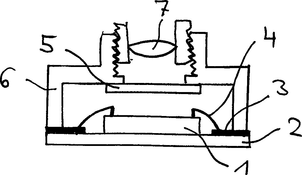
Der
in der
Das
in der vorliegenden Patentanmeldung vorgeschlagene Verfahren ermöglicht demgegenüber eine
deutlich geringere Bauhöhe
des Sensors, die sich mit kostengünstigen Herstellungsschritten realisieren
lässt,
wie sie schematisch in
Der
Sensorchip
Ein
derartiger optischer Sensor kann auf einfache Weise mit einem Trägersubstrat
Bei
einem ausreichend dünnen
Sensorchip kann die Verbindung mit dem Trägersubstrat auch ohne eine
Ausnehmung in dem Trägersubstrat
erfolgen. Vorraussetzung hierfür
ist, dass die Dicke des Sensorchips die elektrisch leitfähige Verbindung
zwischen den äußeren Anschlusselementen
In
einer weiteren Ausgestaltung des optischen Sensors sowie des zugehörigen Verfahrens wird
zusätzlich
eine dielektrische Schicht
Die anschließende Verbindung mit dem Trägersubstrat kann dabei in gleicher Weise erfolgen, wie dies bereits in den vorangehenden Beispielen dargestellt ist. Eine Ausnehmung im Trägersubstrat kann hierbei jedoch nicht genutzt werden.The subsequent Connection to the carrier substrate can be done in the same way as already in the preceding Examples is shown. A recess in the carrier substrate can but not used here.
- 11
- Sensorchipsensor chip
- 22
- Leiterplattecircuit board
- 33
- Leiterbahnenconductor tracks
- 44
- Drahtverbindungwire connection
- 55
- optisch transparente Platteoptical transparent plate
- 66
- Gehäusecasing
- 77
- Linselens
- 1010
- optisch transparente Platteoptical transparent plate
- 1111
- Metallisierungmetallization
- 1212
- erste Anschlussflächenfirst pads
- 1313
- zweite Anschlussflächensecond pads
- 1414
- Leiterbahnenconductor tracks
- 1515
- Anschlussflächen auf dem SensorchipConnection surfaces on the sensor chip
- 1616
- optisch sensitive Flächeoptical sensitive area
- 1717
- Sensorchipsensor chip
- 1818
- anisotrop elektrisch leitender Klebstoffanisotropic electrically conductive adhesive
- 1919
- Trägersubstratcarrier substrate
- 2020
- dielektrische Schichtdielectric layer
- 2121
- Viasvias
- 2222
- Metallisierungmetallization
- 2323
- dritte Anschlussflächenthird pads
- 2424
- Leiterbahnenconductor tracks
Claims (25)
Priority Applications (1)
| Application Number | Priority Date | Filing Date | Title |
|---|---|---|---|
| DE102006059411A DE102006059411A1 (en) | 2006-12-15 | 2006-12-15 | Method for producing optical sensor for mounting on carrier substrate, involves providing optical transparent plate with lateral dimensions larger than sensor chip |
Applications Claiming Priority (1)
| Application Number | Priority Date | Filing Date | Title |
|---|---|---|---|
| DE102006059411A DE102006059411A1 (en) | 2006-12-15 | 2006-12-15 | Method for producing optical sensor for mounting on carrier substrate, involves providing optical transparent plate with lateral dimensions larger than sensor chip |
Publications (1)
| Publication Number | Publication Date |
|---|---|
| DE102006059411A1 true DE102006059411A1 (en) | 2008-06-26 |
Family
ID=39431333
Family Applications (1)
| Application Number | Title | Priority Date | Filing Date |
|---|---|---|---|
| DE102006059411A Ceased DE102006059411A1 (en) | 2006-12-15 | 2006-12-15 | Method for producing optical sensor for mounting on carrier substrate, involves providing optical transparent plate with lateral dimensions larger than sensor chip |
Country Status (1)
| Country | Link |
|---|---|
| DE (1) | DE102006059411A1 (en) |
Citations (2)
| Publication number | Priority date | Publication date | Assignee | Title |
|---|---|---|---|---|
| KR100618941B1 (en) * | 2005-11-08 | 2006-09-01 | 김성규 | Transparent light emitting device and manufacturing method |
| US20060275599A1 (en) * | 2003-01-10 | 2006-12-07 | Hugues Lefevre | Glazing comprising electronics elements |
-
2006
- 2006-12-15 DE DE102006059411A patent/DE102006059411A1/en not_active Ceased
Patent Citations (2)
| Publication number | Priority date | Publication date | Assignee | Title |
|---|---|---|---|---|
| US20060275599A1 (en) * | 2003-01-10 | 2006-12-07 | Hugues Lefevre | Glazing comprising electronics elements |
| KR100618941B1 (en) * | 2005-11-08 | 2006-09-01 | 김성규 | Transparent light emitting device and manufacturing method |
Non-Patent Citations (1)
| Title |
|---|
| LEIB,J: New Wafer-Level-Packaging Technology using Silicon-Via-Contacts for Optical and other Sensor Applications, In: http://www.suss.de/ secap/docs/GeneralTechnologies/SECAP2004-Schott.pd f * |
Similar Documents
| Publication | Publication Date | Title |
|---|---|---|
| EP1364412B1 (en) | Digital camera comprising a light-sensitive sensor | |
| DE69408558T2 (en) | Use of an anisotropic conductive layer for connecting connection conductors of a printed circuit board to the electrical connection contacts of a photoelectric conversion device and method for assembling this device | |
| DE102007017831B4 (en) | Semiconductor module and a method for producing a semiconductor module | |
| DE10045043B4 (en) | Semiconductor component and method for its production | |
| DE10128419B4 (en) | Solid state image pickup device with microlens and underfill | |
| DE10016132A1 (en) | Electronic component with flexible contact points and method for its production | |
| DE102014221650A1 (en) | ELECTRONIC COMPONENT, ELECTRONIC DEVICE AND METHOD FOR PRODUCING THE ELECTRONIC COMPONENT | |
| DE10348620A1 (en) | Semiconductor module with housing contacts | |
| DE102013107725A1 (en) | Smart card module | |
| DE102009041463A1 (en) | Semiconductor device with a plurality of semiconductor substrates and method for their production | |
| DE10144467B4 (en) | Electronic sensor component and method for its production | |
| EP2040295A2 (en) | System with a connection device and at least one semi-conductor construction element | |
| EP0637081A2 (en) | Micro sensor with plug connections | |
| DE3917707A1 (en) | ELECTRONIC MODULE AND METHOD FOR THE PRODUCTION THEREOF | |
| DE10141571B4 (en) | A method of assembling a semiconductor device and integrated circuit fabricated therewith that is suitable for three-dimensional, multi-layered circuits | |
| DE10227544B4 (en) | Device for optical data transmission | |
| WO2009118058A1 (en) | Camera unit for use in a vehicle and method for manufacture thereof | |
| DE102013204814A1 (en) | Photovoltaic module and method of making a photovoltaic module | |
| DE102006059411A1 (en) | Method for producing optical sensor for mounting on carrier substrate, involves providing optical transparent plate with lateral dimensions larger than sensor chip | |
| DE102015120647B4 (en) | Electrical device with thin solder stop layer and method of manufacture | |
| DE102006006825A1 (en) | Semiconductor component e.g. ball grid array semiconductor component, has semiconductor chip with protective casing, and soldering ball arranged in recess of electrical insulating layer and connected with connecting carrier | |
| DE19831876A1 (en) | Producing contact between flexible conductor and substrate | |
| DE19826426C2 (en) | Miniaturized electronic system and method for its manufacture | |
| EP1247250A2 (en) | Chipcard arrangement | |
| EP2575175B1 (en) | Image sensor with large chip size |
Legal Events
| Date | Code | Title | Description |
|---|---|---|---|
| OP8 | Request for examination as to paragraph 44 patent law | ||
| R016 | Response to examination communication | ||
| R002 | Refusal decision in examination/registration proceedings | ||
| R003 | Refusal decision now final |
Effective date: 20110809 |