DE102005039517A1 - Phase delay element and method for producing a phase delay element - Google Patents
Phase delay element and method for producing a phase delay element Download PDFInfo
- Publication number
- DE102005039517A1 DE102005039517A1 DE102005039517A DE102005039517A DE102005039517A1 DE 102005039517 A1 DE102005039517 A1 DE 102005039517A1 DE 102005039517 A DE102005039517 A DE 102005039517A DE 102005039517 A DE102005039517 A DE 102005039517A DE 102005039517 A1 DE102005039517 A1 DE 102005039517A1
- Authority
- DE
- Germany
- Prior art keywords
- plate
- anisotropic crystal
- crystal plate
- phase delay
- delay element
- Prior art date
- Legal status (The legal status is an assumption and is not a legal conclusion. Google has not performed a legal analysis and makes no representation as to the accuracy of the status listed.)
- Withdrawn
Links
- 238000004519 manufacturing process Methods 0.000 title claims abstract description 10
- 239000013078 crystal Substances 0.000 claims abstract description 49
- 238000007654 immersion Methods 0.000 claims abstract description 28
- 239000007788 liquid Substances 0.000 claims abstract description 20
- 239000002178 crystalline material Substances 0.000 claims abstract description 3
- 238000000034 method Methods 0.000 claims description 18
- 239000002904 solvent Substances 0.000 claims description 13
- VYPSYNLAJGMNEJ-UHFFFAOYSA-N Silicium dioxide Chemical compound O=[Si]=O VYPSYNLAJGMNEJ-UHFFFAOYSA-N 0.000 claims description 5
- 238000001459 lithography Methods 0.000 claims description 5
- XDTMQSROBMDMFD-UHFFFAOYSA-N Cyclohexane Chemical compound C1CCCCC1 XDTMQSROBMDMFD-UHFFFAOYSA-N 0.000 claims description 3
- 239000004065 semiconductor Substances 0.000 claims description 3
- 229910018072 Al 2 O 3 Inorganic materials 0.000 claims description 2
- 229910017768 LaF 3 Inorganic materials 0.000 claims description 2
- 229910004298 SiO 2 Inorganic materials 0.000 claims description 2
- 150000001875 compounds Chemical class 0.000 claims description 2
- 239000012530 fluid Substances 0.000 claims description 2
- 238000007517 polishing process Methods 0.000 claims description 2
- 239000003960 organic solvent Substances 0.000 claims 1
- 238000000926 separation method Methods 0.000 claims 1
- 239000000463 material Substances 0.000 description 7
- 230000005540 biological transmission Effects 0.000 description 4
- 239000012535 impurity Substances 0.000 description 3
- LFQSCWFLJHTTHZ-UHFFFAOYSA-N Ethanol Chemical compound CCO LFQSCWFLJHTTHZ-UHFFFAOYSA-N 0.000 description 2
- 239000000853 adhesive Substances 0.000 description 2
- 230000001070 adhesive effect Effects 0.000 description 2
- 230000000694 effects Effects 0.000 description 2
- 230000003287 optical effect Effects 0.000 description 2
- 230000015572 biosynthetic process Effects 0.000 description 1
- 238000002144 chemical decomposition reaction Methods 0.000 description 1
- 230000001419 dependent effect Effects 0.000 description 1
- 238000004090 dissolution Methods 0.000 description 1
- 239000004744 fabric Substances 0.000 description 1
- 238000005286 illumination Methods 0.000 description 1
- 230000007774 longterm Effects 0.000 description 1
- ORUIBWPALBXDOA-UHFFFAOYSA-L magnesium fluoride Chemical compound [F-].[F-].[Mg+2] ORUIBWPALBXDOA-UHFFFAOYSA-L 0.000 description 1
- 230000013011 mating Effects 0.000 description 1
- 230000010287 polarization Effects 0.000 description 1
- 238000002360 preparation method Methods 0.000 description 1
- 230000005855 radiation Effects 0.000 description 1
- 230000000717 retained effect Effects 0.000 description 1
- 239000000126 substance Substances 0.000 description 1
Classifications
-
- G—PHYSICS
- G02—OPTICS
- G02B—OPTICAL ELEMENTS, SYSTEMS OR APPARATUS
- G02B1/00—Optical elements characterised by the material of which they are made; Optical coatings for optical elements
- G02B1/02—Optical elements characterised by the material of which they are made; Optical coatings for optical elements made of crystals, e.g. rock-salt, semi-conductors
-
- G—PHYSICS
- G02—OPTICS
- G02B—OPTICAL ELEMENTS, SYSTEMS OR APPARATUS
- G02B5/00—Optical elements other than lenses
- G02B5/30—Polarising elements
- G02B5/3083—Birefringent or phase retarding elements
- G02B5/3091—Birefringent or phase retarding elements for use in the UV
-
- G—PHYSICS
- G03—PHOTOGRAPHY; CINEMATOGRAPHY; ANALOGOUS TECHNIQUES USING WAVES OTHER THAN OPTICAL WAVES; ELECTROGRAPHY; HOLOGRAPHY
- G03F—PHOTOMECHANICAL PRODUCTION OF TEXTURED OR PATTERNED SURFACES, e.g. FOR PRINTING, FOR PROCESSING OF SEMICONDUCTOR DEVICES; MATERIALS THEREFOR; ORIGINALS THEREFOR; APPARATUS SPECIALLY ADAPTED THEREFOR
- G03F7/00—Photomechanical, e.g. photolithographic, production of textured or patterned surfaces, e.g. printing surfaces; Materials therefor, e.g. comprising photoresists; Apparatus specially adapted therefor
- G03F7/70—Microphotolithographic exposure; Apparatus therefor
- G03F7/70483—Information management; Active and passive control; Testing; Wafer monitoring, e.g. pattern monitoring
- G03F7/7055—Exposure light control in all parts of the microlithographic apparatus, e.g. pulse length control or light interruption
- G03F7/70566—Polarisation control
-
- G—PHYSICS
- G03—PHOTOGRAPHY; CINEMATOGRAPHY; ANALOGOUS TECHNIQUES USING WAVES OTHER THAN OPTICAL WAVES; ELECTROGRAPHY; HOLOGRAPHY
- G03F—PHOTOMECHANICAL PRODUCTION OF TEXTURED OR PATTERNED SURFACES, e.g. FOR PRINTING, FOR PROCESSING OF SEMICONDUCTOR DEVICES; MATERIALS THEREFOR; ORIGINALS THEREFOR; APPARATUS SPECIALLY ADAPTED THEREFOR
- G03F7/00—Photomechanical, e.g. photolithographic, production of textured or patterned surfaces, e.g. printing surfaces; Materials therefor, e.g. comprising photoresists; Apparatus specially adapted therefor
- G03F7/70—Microphotolithographic exposure; Apparatus therefor
- G03F7/708—Construction of apparatus, e.g. environment aspects, hygiene aspects or materials
- G03F7/7095—Materials, e.g. materials for housing, stage or other support having particular properties, e.g. weight, strength, conductivity, thermal expansion coefficient
- G03F7/70958—Optical materials or coatings, e.g. with particular transmittance, reflectance or anti-reflection properties
- G03F7/70966—Birefringence
Landscapes
- Physics & Mathematics (AREA)
- General Physics & Mathematics (AREA)
- Optics & Photonics (AREA)
- Chemical & Material Sciences (AREA)
- Crystallography & Structural Chemistry (AREA)
- Health & Medical Sciences (AREA)
- Engineering & Computer Science (AREA)
- Environmental & Geological Engineering (AREA)
- Epidemiology (AREA)
- Public Health (AREA)
- Polarising Elements (AREA)
Abstract
Die Erfindung betrifft ein Verfahren zur Herstellung eines Phasenverzögerungselementes nullter oder niedriger Ordnung, insbesondere eines Phasenverzögerungselementes für Wellenlängen lambda < 200 nm, wobei das Phasenverzögerungselement aus einem doppelbrechenden kristallinen Material gebildet wird. Dabei wird eine mit einer ersten Trägerplatte (1) über eine erste Verbindungsschicht (2) verbundene anisotrope Kristallplatte (3) auf der ersten Trägerplatte (1) abgewandten Seite mittels einer zweiten Verbindungsschicht (4) mit einer zweiten Trägerplatte (5) verbunden. Die beiden Verbindungsschichten (2, 4) werden nacheinander entfernt und auf die freigelegten Flächen der anisotropen Kristallplatte (3) wird jeweils eine Immersionsflüssigkeit aufgebracht und jeweils eine Stützplatte (8, 13) aufgelegt.The invention relates to a method for producing a zero or low order phase delay element, in particular a phase delay element for wavelengths lambda <200 nm, the phase delay element being formed from a birefringent crystalline material. An anisotropic crystal plate (3) connected to a first carrier plate (1) via a first connecting layer (2) is connected to a second carrier plate (5) by means of a second connecting layer (4) on the side facing away from the first carrier plate (1). The two connecting layers (2, 4) are removed one after the other and an immersion liquid is applied to each of the exposed surfaces of the anisotropic crystal plate (3) and a support plate (8, 13) is placed on each.
Description
Die Erfindung betrifft ein Verfahren zur Herstellung eines Phasenverzögerungselementes nullter oder niedriger Ordnung, insbesondere eines Phasenverzögerungselementes für Wellenlängen von λ<200nm, wobei das Phasenverzögerungselement aus einem doppelbrechenden kristallinen Material gebildet wird. Des Weiteren betrifft die Erfindung ein Phasenverzögerungselement nullter oder niedriger Ordnung.The The invention relates to a method for producing a phase delay element zeroth or low order, in particular a phase delay element for wavelengths of λ <200nm, the Phase delay element is formed from a birefringent crystalline material. Furthermore, the invention relates to a phase delay element zeroth or lower order.
Phasenverzögerungselemente sind optische Komponenten, mit denen der Polarisationszustand des Lichtes definiert verändert werden kann. Für die Halbleiterlithograpie mit Wellenlängen λ<200nm werden Phasenverzögerungselemente nullter Ordnung, also λ/4-Elemente und λ/2-Elemente, benötigt. Einige Spiegellinsenobjektive bzw. Projektionsobjektive für die Halbleiterlithographie ohne zentrale Abschattung mit einem polarisationsoptischen Teiler erreichen ihre höchste Transmission nur dann, wenn entsprechende Phasenverzögerungselemente zur Verfügung stehen.Phase delay elements are optical components with which the polarization state of the light defined changed can be. For the semiconductor lithography with wavelengths λ <200nm become phase delay elements zeroth order, ie λ / 4 elements and λ / 2 elements, needed. Some mirror lenses or projection lenses for semiconductor lithography without central shading with a polarization-optical divider reach their highest Transmission only if appropriate phase delay elements to disposal stand.
Dabei
sind an die Phasenverzögerungselemente
mehrere Bedingungen gleichzeitig zu stellen, durch die die Ausführungsmöglichkeiten
erheblich eingegrenzt sind:
In erster Linie ist eine gute Transmittivität für die Belichtungswellenlängen von
157nm, 193nm und 248nm wünschenswert.
Ferner ist es erforderlich, dass die gewählten Materialien über die
ganze Produktlebensdauer hinweg eine gute Strahlungsbeständigkeit
zeigen. Die Verwendung in einem Beleuchtungssystem bedingt, dass die
verwendeten Elemente sowohl in mechanischer Hinsicht als auch hinsichtlich
der Phasenverzögerung
gegenüber
Temperaturänderungen
unempfindlich sein müssen.In this case, several conditions must be set simultaneously to the phase delay elements, by means of which the possible implementations are considerably limited:
First and foremost, good transmissivity is desirable for the exposure wavelengths of 157nm, 193nm and 248nm. Furthermore, it is necessary that the materials chosen show good radiation resistance throughout the product life. Use in an illumination system requires that the elements used be insensitive to both temperature and mechanical changes in terms of phase delay.
Schließlich müssen die Verzögerungselemente über einen großen Winkelbereich hinweg ihre Verzögerung weitgehend beibehalten, so dass vor allem Phasenverzögerungselemente nullter Ordnung für die genannten Anwendungen geeignet erscheinen.Finally, the Delay elements over one huge Angular range, their delay largely retained, so that especially phase delay elements zero order for the applications mentioned appear suitable.
Aus dem Stand der Technik sind verschiedene Phasenverzögerungselemente und Varianten zu deren Herstellung bekannt.Out The prior art has various phase delay elements and variants for their preparation known.
Beispielsweise ist es üblich, doppelbrechende Materialien wie z.B. Magnesiumfluorid (MgF2) oder Siliziumdioxid (SiO2) in Phasenverzögerungselementen zu verwenden. Da die genannten Materialien stark doppelbrechende Eigenschaften zeigen, ergeben sich für die Dicke der zu verwendenden Platten für die betrachteten Wellenlängen im Bereich < 200nm Werte im Bereich weniger μm. Für die Lithographie sind Mindestgrößen der Phasenverzögerungselemente im Bereich von z.B. 70x160mm bzw. ein Durchmesser von 150-200mm notwendig, so dass bei den genannten Dicken derartige Phasenverzögerungselemente mechanisch ausgesprochen instabil sind und durch kleinste äußere Störungen unbrauchbar werden können.For example, it is common to use birefringent materials such as magnesium fluoride (MgF 2 ) or silica (SiO 2 ) in phase retardation elements. Since the materials mentioned exhibit strongly birefringent properties, the thickness of the plates to be used for the wavelengths considered in the range <200 nm results in values in the range of a few μm. For lithography minimum sizes of the phase delay elements in the range of eg 70x160mm or a diameter of 150-200mm are necessary, so that at the mentioned thicknesses such phase delay elements are mechanically very unstable and can be unusable by the smallest external disturbances.
Ein erster Lösungsansatz für diese Problematik ist in der Internationalen Patentanmeldung WO 2005/024474 A1, die auf die Anmelderin zurückgeht, aufgezeigt. Die oben genannten dünnen Phasenverzögerungselemente werden nach der Lehre der zitierten Schrift dadurch mechanisch stabilisiert, dass die dünne doppelbrechende anisotrope Kristallplatte auf einer transparenten Trägerplatte angesprengt wird, wobei als Trägerplatte für die Wellenlängen 193nm und 248nm beispielsweise eine Quarzglasplatte verwendet werden kann. Dabei werden in der Regel durch die Ansprengkräfte die thermischen Längenänderungen der wesentlich dickeren Trägerplatte auf die anisotrope Kristallplatte nahezu vollständig übertragen, so dass diese den Längenänderungen der Trägerplatte folgt.One first solution for this Problem is in International Patent Application WO 2005/024474 A1, which goes back to the applicant, demonstrated. The above thin ones Phase delay elements are thus mechanically stabilized according to the teaching of the cited document, that the thin birefringent anisotropic crystal plate on a transparent support plate is sprinkled, being used as a support plate for the wavelength 193 nm and 248 nm, for example, a quartz glass plate can be used. In this case, the thermal length changes are usually by the Ansprengkräfte the much thicker carrier plate transferred almost completely to the anisotropic crystal plate, so that this changes in length the carrier plate follows.
Die für die genannte Anwendung in erster Linie in Frage kommenden einachsig doppelbrechenden Kristallmaterialien haben die folgenden Eigenschaften: The for the mentioned application primarily eligible uniaxial Birefringent crystal materials have the following properties:
Doppelbrechung
ne–no: 
Resultierende
Dicken für
eine Platte nullter Ordnung für λ/4(λ/2) [μm]: 
Thermischer
Ausdehnungskoeffizient: 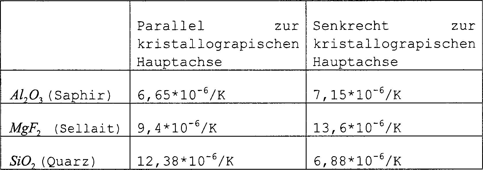
Ein Problem der in der WO 2005/024474 A1 dargestellten Vorgehensweise besteht jedoch darin, dass bereits kleinste Verunreinigungen zwischen Trägerplatte und anisotroper Kristallplatte genügen, um die anisotrope Kristallplatte von der Trägerplatte zumindest lokal abzuheben. Da die Dicke der so entstehenden Spalte zwischen Trägerplatte und anisotroper Kristallplatte üblicherweise den Bereich des optischen Nahfeldes (ca. λ/10) überschreitet, kommt es in den durch die Verunreinigungen abgehobenen Bereichen zu einer Verminderung der Transmission. Aufgrund der zentralen Bedeutung der Dosiseinhaltung für die Qualität des Lithographiesystems sind derartige Effekte – insbesondere bei hierdurch resultierenden Transmissionseinbrüchen im Bereich >7% – häufig nicht mehr zu tolerieren.One Problem of the procedure described in WO 2005/024474 A1 However, it is that even the smallest impurities between support plate and anisotropic crystal plate suffice for the anisotropic crystal plate from the carrier plate at least locally take off. Since the thickness of the resulting gap between support plate and anisotropic crystal plate usually exceeds the range of the optical near field (about λ / 10), it comes in the areas lifted off by the impurities for a reduction the transmission. Due to the central importance of dose compliance for the quality of the lithography system are such effects - especially in this way resulting transmission dips in the range> 7% - often no longer tolerate.
Somit ist es Aufgabe der vorliegenden Erfindung, ein mechanisch stabiles Phasenverzögerungselement sowie ein Verfahren zu dessen Herstellung anzugeben, wobei eine schädliche Verminderung der Transmission vermieden werden soll.Consequently It is an object of the present invention, a mechanically stable Phase delay element and to provide a method for its production, wherein a harmful Reduction of transmission should be avoided.
Diese Aufgabe wird durch ein Verfahren nach Anspruch 1 sowie durch ein Phasenverzögerungselement nach Anspruch 11 gelöst. Die Unteransprüche beziehen sich auf vorteilhafte weitere Varianten der Erfindung.These The object is achieved by a method according to claim 1 and by a Phase delay element solved according to claim 11. The dependent claims refer to advantageous further variants of the invention.
Erfindungsgemäß wird die anisotrope Kristallplatte zwischen zwei Stützplatten mechanisch gelagert eingebracht. Dies hat den Vorteil, dass größere Deformationen der anisotropen Kristallplatte auf diese Weise wirksam vermieden werden können. Um unkontrollierte Bewegungen der anisotropen Kristallplatte zwischen den Stützplatten zu vermeiden, wird der Raum zwischen den Stützplatten und der Kristallplatte mit einer Immersionsflüssigkeit ausgefüllt. Dabei ist es vorteilhaft, die Brechzahl der Immersionsflüssigkeit im Bereich der Brechzahl des ordentlichen Strahls no und der des außerordentlichen Strahls ne zu wählen.According to the invention, the anisotropic crystal plate is mechanically supported between two support plates brought in. This has the advantage that larger deformations of the anisotropic crystal plate can be effectively avoided in this way. In order to avoid uncontrolled movements of the anisotropic crystal plate between the support plates, the space between the support plates and the crystal plate is filled with an immersion liquid. It is advantageous to choose the refractive index of the immersion liquid in the range of the refractive index of the ordinary ray n o and that of the extraordinary ray n e .
Ausführungsbeispiele der Erfindung werden nachfolgend anhand der Zeichnungen exemplarisch erläutert.embodiments The invention will be exemplified below with reference to the drawings explained.
Es zeigen:It demonstrate:
Zur
Herstellung des erfindungsgemäßen Phasenverzögerungselementes
wird zunächst
das in der WO 2005/024474 A1 dargestellte Verfahren bis zu dem Arbeitsschritt
durchgeführt,
nach dem eine anisotrope Kristallplatte
Hierzu
wird eine erste Trägerplatte
Nachfolgend
wird ein Großteil
der anisotropen Kristallplatte
Die
Kristallplatte
Die
Verbindungsschicht
Die
nachfolgend aufzubringende zweite Verbindungsschicht
Nach
der Aushärtung
der zweiten Verbindungsschicht
Durch
einen nachfolgenden Läppvorgang
können
evtl. verbliebene Reste der Trägerplatte
Die
freigelegte erste Verbindungsschicht
Auf
die so freigelegte Fläche
der Kristallplatte
Anschließend wird
das System aus erster Stützplatte
Nach
dem Auflösen
der Verbindungsschicht
Anschließend kann
eine zweite Stützplatte
Sobald die gewünschte Dicke des Immersionsfilmes erreicht ist, kann die gesamte Anordnung mechanisch gehaltert werden.As soon as the desired Thickness of the immersion film is achieved, the entire arrangement be held mechanically.
Das
so erhaltene Phasenverzögerungselement
ist in
Die
anisotrope Kristallplatte
Die beschriebene Erfindung ermöglicht damit die Bereitstellung mechanisch robuster, großflächiger Phasenverzögerungselemente hoher Qualität und Langzeitstabilität.The described invention allows thus the provision of mechanically robust, large-scale phase delay elements high quality and long-term stability.
Claims (19)
Priority Applications (2)
| Application Number | Priority Date | Filing Date | Title |
|---|---|---|---|
| DE102005039517A DE102005039517A1 (en) | 2005-08-20 | 2005-08-20 | Phase delay element and method for producing a phase delay element |
| US11/465,244 US20070039543A1 (en) | 2005-08-20 | 2006-08-17 | Phase delay element and method for producing a phase delay element |
Applications Claiming Priority (1)
| Application Number | Priority Date | Filing Date | Title |
|---|---|---|---|
| DE102005039517A DE102005039517A1 (en) | 2005-08-20 | 2005-08-20 | Phase delay element and method for producing a phase delay element |
Publications (1)
| Publication Number | Publication Date |
|---|---|
| DE102005039517A1 true DE102005039517A1 (en) | 2007-02-22 |
Family
ID=37697415
Family Applications (1)
| Application Number | Title | Priority Date | Filing Date |
|---|---|---|---|
| DE102005039517A Withdrawn DE102005039517A1 (en) | 2005-08-20 | 2005-08-20 | Phase delay element and method for producing a phase delay element |
Country Status (2)
| Country | Link |
|---|---|
| US (1) | US20070039543A1 (en) |
| DE (1) | DE102005039517A1 (en) |
Cited By (1)
| Publication number | Priority date | Publication date | Assignee | Title |
|---|---|---|---|---|
| DE102007027811A1 (en) * | 2007-06-13 | 2008-12-24 | Carl Zeiss Smt Ag | Optical element has partial components connecting intermediate layer provided area by area between partial components, where intermediate layer is formed as inorganic layer and contains silicon oxide bridges |
Families Citing this family (1)
| Publication number | Priority date | Publication date | Assignee | Title |
|---|---|---|---|---|
| JP2007515657A (en) * | 2003-09-09 | 2007-06-14 | カール・ツァイス・エスエムティー・アーゲー | Phase lag element and method of manufacturing phase lag element |
Family Cites Families (43)
| Publication number | Priority date | Publication date | Assignee | Title |
|---|---|---|---|---|
| NL213657A (en) * | 1956-08-14 | |||
| FR1542515A (en) * | 1966-07-21 | 1968-09-09 | Ibm | Self-adjusting mount for optical framing |
| US3864111A (en) * | 1973-08-08 | 1975-02-04 | James C Kemp | Reducing Stress Birefringence in Fused Silica Optical Elements |
| US4407566A (en) * | 1981-09-29 | 1983-10-04 | Lockheed Missiles & Space Co., Inc. | Optical filter |
| US4767479A (en) * | 1987-09-21 | 1988-08-30 | United Technologies Corporation | Method for bonding ceramic casting cores |
| JPH06324298A (en) * | 1993-03-31 | 1994-11-25 | Citizen Watch Co Ltd | Optical device |
| JP3280804B2 (en) * | 1994-08-15 | 2002-05-13 | 触媒化成工業株式会社 | Method of forming particle layer on substrate, method of flattening uneven surface of substrate, and substrate with particle layer |
| DE19637563A1 (en) * | 1996-09-14 | 1998-03-19 | Zeiss Carl Fa | Birefringent faceplate arrangement and DUV quarter-wave plate |
| DE19704936A1 (en) * | 1997-02-10 | 1998-08-13 | Zeiss Carl Fa | Optical link and manufacturing process |
| US5919552A (en) * | 1997-05-07 | 1999-07-06 | Xerox Corporation | Coated substrates and methods |
| JP3458763B2 (en) * | 1998-05-29 | 2003-10-20 | 株式会社豊田中央研究所 | Birefringent plate |
| US6480250B1 (en) * | 1999-06-02 | 2002-11-12 | Fuji Photo Film Co., Ltd. | Low-reflection transparent conductive multi layer film having at least one transparent protective layer having anti-smudge properties |
| US7039695B1 (en) * | 2000-04-28 | 2006-05-02 | Microsoft Corporation | System and method for archiving within a client management tool |
| US6885423B2 (en) * | 2000-12-06 | 2005-04-26 | Nitto Denko Corporation | Method for manufacturing homeotropic alignment liquid crystal film |
| US20020191291A1 (en) * | 2000-12-08 | 2002-12-19 | Bin Zhao | Birefringent devices and filters of temperature compensation |
| US6947215B2 (en) * | 2001-12-27 | 2005-09-20 | Canon Kabushiki Kaisha | Optical element, optical functional device, polarization conversion device, image display apparatus, and image display system |
| TW589466B (en) * | 2002-03-25 | 2004-06-01 | Zeon Corp | Optical film and process for producing the same |
| WO2004038477A1 (en) * | 2002-10-24 | 2004-05-06 | Fuji Photo Film Co., Ltd. | Process for producing cellulose acylate film |
| JP2004264620A (en) * | 2003-03-03 | 2004-09-24 | Jsr Corp | Laminated wave plate |
| WO2004106057A1 (en) * | 2003-05-27 | 2004-12-09 | Exxonmobil Chemical Patents Inc. | Backing layers and substrates for articles formed from ionomer laminates |
| US7071022B2 (en) * | 2003-07-18 | 2006-07-04 | Corning Incorporated | Silicon crystallization using self-assembled monolayers |
| JP4265766B2 (en) * | 2003-08-25 | 2009-05-20 | 東京応化工業株式会社 | Resist protective film forming material for immersion exposure process, resist protective film comprising the protective film forming material, and resist pattern forming method using the resist protective film |
| JP2007515657A (en) * | 2003-09-09 | 2007-06-14 | カール・ツァイス・エスエムティー・アーゲー | Phase lag element and method of manufacturing phase lag element |
| WO2005066672A1 (en) * | 2003-12-05 | 2005-07-21 | 3M Innovative Properties Company | Process for producing photonic crystals and controlled defects therein |
| JP4770464B2 (en) * | 2003-12-18 | 2011-09-14 | 株式会社大真空 | Optical filter |
| US20080062355A1 (en) * | 2003-12-25 | 2008-03-13 | Fuji Photo Film Co., Ltd. | Polarizing Plate and Liquid Crystal Display |
| US7504139B2 (en) * | 2003-12-26 | 2009-03-17 | Fujifilm Corporation | Optical cellulose acylate film, polarizing plate and liquid crystal display |
| US7023520B2 (en) * | 2004-06-18 | 2006-04-04 | Charmica Photoelectronic Co., Ltd. | Method and system for fabricating liquid crystal film and method for fabricating brightening film |
| US20060008588A1 (en) * | 2004-07-12 | 2006-01-12 | Marc Chilla | Process for the production of multi-layer coatings |
| KR101146521B1 (en) * | 2004-07-19 | 2012-05-25 | 삼성전자주식회사 | Phase delay element, method for manufacturing thereof, substrate having the same and method for manufacturing thereof, and light providing method and liquid crystal display using the same |
| JPWO2006018986A1 (en) * | 2004-08-18 | 2008-05-08 | コニカミノルタエムジー株式会社 | Holographic recording medium, holographic recording method, and holographic information medium |
| US20060068116A1 (en) * | 2004-09-27 | 2006-03-30 | Marc Chilla | Process for the production of multi-layer coatings in light metallic color shades |
| US20060069192A1 (en) * | 2004-09-29 | 2006-03-30 | Konica Minolta Opto, Inc. | Method for manufacturing cellulose ester film, and cellulose ester film, optical film, polarizing plate and liquid crystal display device using the same |
| JP2006113175A (en) * | 2004-10-13 | 2006-04-27 | Konica Minolta Opto Inc | Optical film, polarizing plate and display apparatus |
| JP5470672B2 (en) * | 2004-12-09 | 2014-04-16 | コニカミノルタ株式会社 | Method for producing cellulose ester film |
| US20060165919A1 (en) * | 2005-01-27 | 2006-07-27 | Fuji Photo Film Co., Ltd. | Coating composition, optical film, anti-reflection film, polarizing plate and image display device using the same |
| JP4520418B2 (en) * | 2005-02-18 | 2010-08-04 | キヤノン株式会社 | Optical transparent member and optical system using the same |
| TW200643489A (en) * | 2005-03-10 | 2006-12-16 | Konica Minolta Opto Inc | Optical film, manufacturing method of optical film, optical compensating film, manufacturing method of optical compensating film, polarizing plate, and liquid crystal display |
| JP4736562B2 (en) * | 2005-06-23 | 2011-07-27 | コニカミノルタオプト株式会社 | Polarizing plate and display device |
| WO2007026524A1 (en) * | 2005-08-30 | 2007-03-08 | Konica Minolta Opto, Inc. | Polarizing plate and liquid crystal display device manufactured using the same |
| JP2007266074A (en) * | 2006-03-27 | 2007-10-11 | Toshiba Corp | Semiconductor device manufacturing method and immersion lithography system |
| WO2007148554A1 (en) * | 2006-06-21 | 2007-12-27 | Konica Minolta Opto, Inc. | Polarizing plate protective film, polarizing plate, and liquid crystal display |
| JP2008063536A (en) * | 2006-09-11 | 2008-03-21 | Fujifilm Corp | Cyclic olefin resin film |
-
2005
- 2005-08-20 DE DE102005039517A patent/DE102005039517A1/en not_active Withdrawn
-
2006
- 2006-08-17 US US11/465,244 patent/US20070039543A1/en not_active Abandoned
Cited By (1)
| Publication number | Priority date | Publication date | Assignee | Title |
|---|---|---|---|---|
| DE102007027811A1 (en) * | 2007-06-13 | 2008-12-24 | Carl Zeiss Smt Ag | Optical element has partial components connecting intermediate layer provided area by area between partial components, where intermediate layer is formed as inorganic layer and contains silicon oxide bridges |
Also Published As
| Publication number | Publication date |
|---|---|
| US20070039543A1 (en) | 2007-02-22 |
Similar Documents
| Publication | Publication Date | Title |
|---|---|---|
| DE102005030338B4 (en) | A method of fabricating a liquid crystal display using a femtosecond laser thin film etching process | |
| EP0478055A2 (en) | Process for making at least one trench in a substrate layer | |
| DE60215897T2 (en) | Internally marked quartz glass and marking process | |
| DE10223113A1 (en) | Photolithographic mask with structure and absorber, for structurization of photosensitive material, e.g. on wafer, has chemically- and mechanically-stable protective coating, preferably applied by atomic layer chemical vapor deposition | |
| EP3592501B1 (en) | Method for producing a technical mask | |
| EP0104685B1 (en) | Method of manufacturing a mask for obtaining texturised patterns in resist layers using x-ray lithography | |
| EP2685325B1 (en) | Spiral spring, method for producing the same, applications and micromechanical drives | |
| DE112004002199B4 (en) | A method of making an extreme ultraviolet radiation reflective mask using atomic force microscope lithography | |
| DE102015208831B4 (en) | Method for producing an EUV module, EUV module and EUV lithography system | |
| DE102007059258A1 (en) | Microlithographic projection exposure system has double-refractive delay system with time-delay element, which has component is made of optically positive uniaxial crystal material with optical crystal axis | |
| DE102012204833A1 (en) | Mirror i.e. facet mirror, for use in lighting system for projection exposure system, has layer partially formed from graphene and arranged as finishing layer on layer arrangement, and substrate made of material e.g. glass and ceramic | |
| DE102005039517A1 (en) | Phase delay element and method for producing a phase delay element | |
| DE102004038548A1 (en) | Mask blank manufacturing method for photolithography processing, involves designing handling portion so that multilayered layer on front surface of substrate is exposed in each handling portion and pressed by mechanical clamp | |
| DE2123887C3 (en) | ||
| DE102012200454A1 (en) | Method for manufacturing reflective optical element for extreme ultraviolet lithography for manufacturing of semiconductor devices, involves providing substrate, applying releasing layer, and applying layer with optical function | |
| DE102012207141A1 (en) | Method for repairing optical elements and optical element | |
| DE102006021334B3 (en) | Polarization-influencing optical elements manufacturing method, involves assembling two components, and non-plane surface of component is provided with defined elevator profile is assembled to plane surface of other component | |
| DE102016125771A1 (en) | Production of air gap areas in multi-component lens systems | |
| DE102006013560A1 (en) | Projection lens for micro lithographic projection illumination system, has lens , to characterizes symmetry axis of another lens by rotation of orientation of crystal axes, where lenses are separated by gap filled with liquid | |
| EP0940718A2 (en) | Reticle with crystalline substrate and pellicle | |
| DE102007019831A1 (en) | Illumination device of a microlithographic projection exposure apparatus | |
| EP2265980A2 (en) | Diffractive element with high wave-front flatness | |
| DE19757560A1 (en) | Process for producing a porous layer using an electrochemical etching process | |
| DE10345476B4 (en) | Lithographic mask and method for covering a mask layer | |
| EP3523696B1 (en) | Composite plate with barrier layer and method for producing a high pressure plate |
Legal Events
| Date | Code | Title | Description |
|---|---|---|---|
| 8127 | New person/name/address of the applicant |
Owner name: CARL ZEISS SMT GMBH, 73447 OBERKOCHEN, DE |
|
| R012 | Request for examination validly filed |
Effective date: 20120419 |
|
| R120 | Application withdrawn or ip right abandoned |