DE102004059467A1 - Gate made of organic field effect transistors - Google Patents
Gate made of organic field effect transistors Download PDFInfo
- Publication number
- DE102004059467A1 DE102004059467A1 DE102004059467A DE102004059467A DE102004059467A1 DE 102004059467 A1 DE102004059467 A1 DE 102004059467A1 DE 102004059467 A DE102004059467 A DE 102004059467A DE 102004059467 A DE102004059467 A DE 102004059467A DE 102004059467 A1 DE102004059467 A1 DE 102004059467A1
- Authority
- DE
- Germany
- Prior art keywords
- electronic component
- effect transistors
- component according
- field effect
- layers
- Prior art date
- Legal status (The legal status is an assumption and is not a legal conclusion. Google has not performed a legal analysis and makes no representation as to the accuracy of the status listed.)
- Ceased
Links
- 230000005669 field effect Effects 0.000 title claims abstract description 77
- 239000010410 layer Substances 0.000 claims abstract description 151
- 239000004065 semiconductor Substances 0.000 claims abstract description 84
- 239000000758 substrate Substances 0.000 claims abstract description 27
- 239000012212 insulator Substances 0.000 claims abstract description 21
- 239000007788 liquid Substances 0.000 claims abstract description 17
- 238000007639 printing Methods 0.000 claims abstract description 14
- 239000000463 material Substances 0.000 claims description 23
- 229920000642 polymer Polymers 0.000 claims description 14
- 230000000295 complement effect Effects 0.000 claims description 6
- 239000002105 nanoparticle Substances 0.000 claims description 6
- 239000002904 solvent Substances 0.000 claims description 6
- 230000008878 coupling Effects 0.000 claims description 4
- 238000010168 coupling process Methods 0.000 claims description 4
- 238000005859 coupling reaction Methods 0.000 claims description 4
- 239000012044 organic layer Substances 0.000 claims description 4
- 239000000976 ink Substances 0.000 claims description 3
- 150000003384 small molecules Chemical class 0.000 claims description 3
- 230000035699 permeability Effects 0.000 claims description 2
- 239000002346 layers by function Substances 0.000 abstract description 2
- 239000004020 conductor Substances 0.000 description 15
- 238000000034 method Methods 0.000 description 15
- 230000008569 process Effects 0.000 description 10
- 238000010586 diagram Methods 0.000 description 9
- 238000004519 manufacturing process Methods 0.000 description 9
- 238000013461 design Methods 0.000 description 8
- 230000015572 biosynthetic process Effects 0.000 description 6
- 239000010408 film Substances 0.000 description 5
- 239000000969 carrier Substances 0.000 description 4
- SLIUAWYAILUBJU-UHFFFAOYSA-N pentacene Chemical compound C1=CC=CC2=CC3=CC4=CC5=CC=CC=C5C=C4C=C3C=C21 SLIUAWYAILUBJU-UHFFFAOYSA-N 0.000 description 4
- 239000000725 suspension Substances 0.000 description 4
- 238000012549 training Methods 0.000 description 4
- XUIMIQQOPSSXEZ-UHFFFAOYSA-N Silicon Chemical compound [Si] XUIMIQQOPSSXEZ-UHFFFAOYSA-N 0.000 description 3
- 239000002800 charge carrier Substances 0.000 description 3
- 239000006185 dispersion Substances 0.000 description 3
- 239000000839 emulsion Substances 0.000 description 3
- 239000011368 organic material Substances 0.000 description 3
- 238000007649 pad printing Methods 0.000 description 3
- 229910052710 silicon Inorganic materials 0.000 description 3
- 239000010703 silicon Substances 0.000 description 3
- XMWRBQBLMFGWIX-UHFFFAOYSA-N C60 fullerene Chemical class C12=C3C(C4=C56)=C7C8=C5C5=C9C%10=C6C6=C4C1=C1C4=C6C6=C%10C%10=C9C9=C%11C5=C8C5=C8C7=C3C3=C7C2=C1C1=C2C4=C6C4=C%10C6=C9C9=C%11C5=C5C8=C3C3=C7C1=C1C2=C4C6=C2C9=C5C3=C12 XMWRBQBLMFGWIX-UHFFFAOYSA-N 0.000 description 2
- XLOMVQKBTHCTTD-UHFFFAOYSA-N Zinc monoxide Chemical compound [Zn]=O XLOMVQKBTHCTTD-UHFFFAOYSA-N 0.000 description 2
- 230000008901 benefit Effects 0.000 description 2
- 238000009835 boiling Methods 0.000 description 2
- 239000003990 capacitor Substances 0.000 description 2
- 238000010276 construction Methods 0.000 description 2
- 230000007547 defect Effects 0.000 description 2
- 230000001419 dependent effect Effects 0.000 description 2
- 230000000694 effects Effects 0.000 description 2
- 238000007646 gravure printing Methods 0.000 description 2
- 239000004922 lacquer Substances 0.000 description 2
- 239000000203 mixture Substances 0.000 description 2
- 230000003287 optical effect Effects 0.000 description 2
- 238000007650 screen-printing Methods 0.000 description 2
- 238000012546 transfer Methods 0.000 description 2
- OKTJSMMVPCPJKN-UHFFFAOYSA-N Carbon Chemical compound [C] OKTJSMMVPCPJKN-UHFFFAOYSA-N 0.000 description 1
- OAKJQQAXSVQMHS-UHFFFAOYSA-N Hydrazine Chemical compound NN OAKJQQAXSVQMHS-UHFFFAOYSA-N 0.000 description 1
- 238000002679 ablation Methods 0.000 description 1
- 239000008186 active pharmaceutical agent Substances 0.000 description 1
- 229910021417 amorphous silicon Inorganic materials 0.000 description 1
- 229910052799 carbon Inorganic materials 0.000 description 1
- 230000008859 change Effects 0.000 description 1
- 238000000576 coating method Methods 0.000 description 1
- 229920001940 conductive polymer Polymers 0.000 description 1
- 239000000470 constituent Substances 0.000 description 1
- 238000010924 continuous production Methods 0.000 description 1
- 229910021419 crystalline silicon Inorganic materials 0.000 description 1
- 230000007423 decrease Effects 0.000 description 1
- 238000000151 deposition Methods 0.000 description 1
- 230000008021 deposition Effects 0.000 description 1
- 238000011161 development Methods 0.000 description 1
- 230000005684 electric field Effects 0.000 description 1
- 238000005516 engineering process Methods 0.000 description 1
- 238000005530 etching Methods 0.000 description 1
- 230000008020 evaporation Effects 0.000 description 1
- 238000001704 evaporation Methods 0.000 description 1
- 229910052732 germanium Inorganic materials 0.000 description 1
- GNPVGFCGXDBREM-UHFFFAOYSA-N germanium atom Chemical compound [Ge] GNPVGFCGXDBREM-UHFFFAOYSA-N 0.000 description 1
- PCHJSUWPFVWCPO-UHFFFAOYSA-N gold Chemical compound [Au] PCHJSUWPFVWCPO-UHFFFAOYSA-N 0.000 description 1
- 229910052737 gold Inorganic materials 0.000 description 1
- 239000010931 gold Substances 0.000 description 1
- AMGQUBHHOARCQH-UHFFFAOYSA-N indium;oxotin Chemical compound [In].[Sn]=O AMGQUBHHOARCQH-UHFFFAOYSA-N 0.000 description 1
- 238000009413 insulation Methods 0.000 description 1
- 229910052751 metal Inorganic materials 0.000 description 1
- 239000002184 metal Substances 0.000 description 1
- 238000001465 metallisation Methods 0.000 description 1
- -1 organometallic organic compounds Chemical class 0.000 description 1
- 230000003647 oxidation Effects 0.000 description 1
- 238000007254 oxidation reaction Methods 0.000 description 1
- 150000002964 pentacenes Chemical class 0.000 description 1
- 229920006255 plastic film Polymers 0.000 description 1
- 239000002985 plastic film Substances 0.000 description 1
- 229920000767 polyaniline Polymers 0.000 description 1
- 229920006267 polyester film Polymers 0.000 description 1
- 229920006254 polymer film Polymers 0.000 description 1
- 239000013047 polymeric layer Substances 0.000 description 1
- 229920000128 polypyrrole Polymers 0.000 description 1
- 229920001296 polysiloxane Polymers 0.000 description 1
- 229920000123 polythiophene Polymers 0.000 description 1
- 238000002360 preparation method Methods 0.000 description 1
- 230000000284 resting effect Effects 0.000 description 1
- 230000035939 shock Effects 0.000 description 1
- 229910052709 silver Inorganic materials 0.000 description 1
- 239000004332 silver Substances 0.000 description 1
- 239000007787 solid Substances 0.000 description 1
- 239000000126 substance Substances 0.000 description 1
- 238000002207 thermal evaporation Methods 0.000 description 1
- 239000010409 thin film Substances 0.000 description 1
- 239000011787 zinc oxide Substances 0.000 description 1
Classifications
-
- H—ELECTRICITY
- H10—SEMICONDUCTOR DEVICES; ELECTRIC SOLID-STATE DEVICES NOT OTHERWISE PROVIDED FOR
- H10K—ORGANIC ELECTRIC SOLID-STATE DEVICES
- H10K19/00—Integrated devices, or assemblies of multiple devices, comprising at least one organic element specially adapted for rectifying, amplifying, oscillating or switching, covered by group H10K10/00
- H10K19/10—Integrated devices, or assemblies of multiple devices, comprising at least one organic element specially adapted for rectifying, amplifying, oscillating or switching, covered by group H10K10/00 comprising field-effect transistors
-
- H—ELECTRICITY
- H10—SEMICONDUCTOR DEVICES; ELECTRIC SOLID-STATE DEVICES NOT OTHERWISE PROVIDED FOR
- H10K—ORGANIC ELECTRIC SOLID-STATE DEVICES
- H10K10/00—Organic devices specially adapted for rectifying, amplifying, oscillating or switching; Organic capacitors or resistors having potential barriers
- H10K10/40—Organic transistors
- H10K10/46—Field-effect transistors, e.g. organic thin-film transistors [OTFT]
- H10K10/462—Insulated gate field-effect transistors [IGFETs]
-
- H—ELECTRICITY
- H10—SEMICONDUCTOR DEVICES; ELECTRIC SOLID-STATE DEVICES NOT OTHERWISE PROVIDED FOR
- H10K—ORGANIC ELECTRIC SOLID-STATE DEVICES
- H10K19/00—Integrated devices, or assemblies of multiple devices, comprising at least one organic element specially adapted for rectifying, amplifying, oscillating or switching, covered by group H10K10/00
- H10K19/20—Integrated devices, or assemblies of multiple devices, comprising at least one organic element specially adapted for rectifying, amplifying, oscillating or switching, covered by group H10K10/00 comprising components having an active region that includes an inorganic semiconductor
-
- H—ELECTRICITY
- H10—SEMICONDUCTOR DEVICES; ELECTRIC SOLID-STATE DEVICES NOT OTHERWISE PROVIDED FOR
- H10K—ORGANIC ELECTRIC SOLID-STATE DEVICES
- H10K71/00—Manufacture or treatment specially adapted for the organic devices covered by this subclass
- H10K71/10—Deposition of organic active material
- H10K71/12—Deposition of organic active material using liquid deposition, e.g. spin coating
Landscapes
- Chemical & Material Sciences (AREA)
- Inorganic Chemistry (AREA)
- Engineering & Computer Science (AREA)
- Manufacturing & Machinery (AREA)
- Thin Film Transistor (AREA)
Abstract
Es wird ein Elektronikbauteil, insbesondere RFID-Transponder, mit mindestens einem Logik-Gatter (3) beschrieben, bei dem das Logik-Gatter (3) aus mehreren auf einem gemeinsamen Substrat (10) aufgebrachten Schichten gebildet ist, die zumindest zwei Elektrodenschichten, zumindest eine aus einer Flüssigkeit aufgebrachte, insbesondere organische, Halbleiterschicht (13, 23) und eine Isolatorschicht (14, 24) umfassen und die so ausgebildet sind, daß das Logik-Gatter mindestens zwei unterschiedlich aufgebaute Feldeffekttransistoren (1, 2) umfaßt. Die Feldeffekttransistoren (1, 2) sind aus mehreren funktionalen Schichten ausgebildet, die auf ein Trägersubstrat (10) durch Drucken oder Rakeln aufbringbar sind.It is an electronic component, in particular RFID transponder, with at least a logic gate (3) described in which the logic gate (3) off a plurality of layers applied to a common substrate (10) is formed, the at least two electrode layers, at least one from a liquid Applied, in particular organic, semiconductor layer (13, 23) and an insulator layer (14, 24) and formed so are that that Logic gate at least two differently constructed field effect transistors (1, 2). The field effect transistors (1, 2) are made of several functional Layers formed on a carrier substrate (10) by printing or doctoring are applicable.
Description
Die Erfindung betrifft ein Elektronikbauteil, insbesondere RFID-Transponder, mit mindestens einem aus organischen Feldeffekttransistoren gebildeten Logik-Gatter.The The invention relates to an electronic component, in particular an RFID transponder, with at least one formed of organic field effect transistors Logic gates.
Das einfachste Logik-Gatter ist der Inverter, aus dem durch Kombination mit weiteren Invertern und/oder weiteren elektronischen Bauelementen alle komplexen Logik-Gatter, wie beispielsweise ANDs, NANDs, NORs und dergleichen gebildet sein können. Organische Logik-Gatter mit nur einer Art Halbleiter – typischerweise handelt es sich um p-Halbleiter – als aktive Schicht sind anfällig gegen Parameterschwankungen der einzelnen Bauteile. Das kann bedeuten, daß diese Schaltungen unzuverlässig oder überhaupt nicht arbeiten, sobald einzelne Bauteile, wie Transistoren, die vom Schaltungsdesign ermittelten Spezifikationen aufgrund von Abweichungen im Herstellungsprozeß nicht ausreichend erfüllen können. Zudem fließt in diesen nur auf einer Halbleiterart basierenden Schaltungen je nach verwendetem Schaltungskonzept zumindest während der Hälfte der Betriebszeit ein dissipativer Strom, d.h. ein Strom, der nicht aus der Funktion der Schaltung begründet ist. Dadurch ist der Leistungsverbrauch deutlich höher als eigentlich notwendig.The The simplest logic gate is the inverter, from which by combination with further inverters and / or further electronic components all complex logic gates, such as ANDs, NANDs, NORs and the like may be formed. Organic logic gates with only one type of semiconductor - typically These are p-type semiconductors - as an active layer are susceptible to Parameter fluctuations of the individual components. That may mean that these Circuits unreliable or at all do not work as soon as individual components, such as transistors, the Specifications determined by the circuit design due to deviations not in the manufacturing process sufficiently fulfill can. In addition, flows in these circuits based on a semiconductor type only according to the circuit concept used a dissipative at least during half of the operating time Current, i. a current that does not depend on the function of the circuit justified is. As a result, the power consumption is much higher than actually necessary.
Solche Logik-Gatter sind beispielsweise für RFID-Transponder (RFID = Radio Frequency Identification) ungeeignet, denn die RFID-Transponder beziehen ihre Versorgungsspannung aus einem mit einer kleinen Antenne empfangenen und sodann gleichgerichteten Hochfrequenzsignal. RFID-Transponder finden zunehmend Anwendung, um Waren oder Sicherheitsdokumente mit elektronisch auslesbaren Informationen zu versehen. Sie finden so beispielsweise Anwendung als elektronischer Strichcode für Konsumgüter, als Kofferanhänger zur Identifikation von Gepäck oder als in den Einband eines Reisepasses eingearbeitetes Sicherheitselement, das Authentifizierungsinformationen speichert.Such Logic gates are used, for example, for RFID transponders (RFID = Radio Frequency Identification) unsuitable, because the RFID transponder draw their supply voltage from one with a small antenna received and then rectified high frequency signal. RFID transponder are increasingly being used to carry goods or security documents provide electronically readable information. They think so For example, use as electronic barcode for consumer goods, as luggage tags for the identification of luggage or as incorporated into the cover of a passport security element, the Stores authentication information.
In dem Dokument KLAUK, H. et al.: Pentacene Thin Film Transistors and Inverter Circuits. In: IEDM Tech. Dig., Dez. 1997, S. 539-542 ist ein Inverter mit gleichartigen organischen Feldeffekttransistoren beschrieben, der aus einem Lade-Feldeftekttransistor und einem Schalt-Feldeffekttransistor, die in Reihe geschaltet sind, ausgebildet ist. Die Herstellung der Feldeftekttransistoren ist durch thermische Abscheidung des organischen Halbleitermaterials vorgesehen.In the document KLAUK, H. et al .: Pentacene Thin Film Transistors and Inverter Circuits. In: IEDM tech. Dig., Dec. 1997, pp. 539-542 an inverter with similar organic field effect transistors described consisting of a charging field effect transistor and a switching field effect transistor, which are connected in series, is formed. The production of Feldeftekttransistoren is by thermal deposition of the organic Semiconductor material provided.
Es sind auch Kombinationen von verschiedenen Halbleitern für Logik-Gatter bekannt, doch wurden bisher nur organische mit anorganischen Halbleitern, beispielsweise beschrieben in dem Dokument BONSE, M. et al.: Integrated a-Si:H/Pentacene Inorganic/Organic Complementary Circuits. In: IEEE IEDM 98, 1998, S. 249-252, oder organische mit metall-organischen Halbleitern verknüpft, wie das Dokument CRONE, B. K. et al,: Design and fabrication of organic complementary circuits. In: J. Appl. Phys.. Vol. 89 Mai 2001, S. 5125-5132 berichtet. Als Herstellungsmethode für die Feldeffekt-Transistoren ist in beiden Dokumenten ebenfalls thermische Abscheidung des organischen Halbleiters vorgesehen.It are also combinations of different semiconductors for logic gates known, but so far only organic with inorganic semiconductors, for example, described in the document BONSE, M. et al .: Integrated a-Si: H / pentacenes Inorganic / Organic Complementary Circuits. In: IEEE IEDM 98, 1998, Pp. 249-252, or organic linked to metal-organic semiconductors, such as the document CRONE, B.K. et al.: Design and fabrication of organic complementary circuits. In: J. Appl. Phys. Vol. 89 May 2001, p. 5125-5132 reports. As a production method for the field effect transistors are also thermal in both documents Deposition of the organic semiconductor provided.
Aufgabe der vorliegenden Erfindung ist es, ein verbessertes Elektronikbauteil unter Verwendung von Feldeffekttransistoren anzugeben.task The present invention is an improved electronic component indicate using field effect transistors.
Erfindungsgemäß wird diese Aufgabe gelöst, indem ein Elektronikbauteil mit mindestens einem Logik-Gatter ausgebildet ist, wobei das Logik-Gatter aus mehreren auf einem gemeinsamen Substrat aufgebrachten Schichten gebildet ist, die zumindest zwei Elektrodenschichten, zumindest eine aus einer Flüssigkeit aufgebrachte, insbesondere organische, Halbleiterschicht und eine Isolatorschicht umfassen und die so ausgebildet sind, daß das Logik-Gatter mindestens zwei unterschiedlich aufgebaute Feldeffekttransistoren umfaßt.According to the invention this Task solved by an electronic component formed with at least one logic gate is, wherein the logic gate of several on a common substrate deposited layers is formed, the at least two electrode layers, at least one of a liquid applied, in particular organic, semiconductor layer and a Insulator layer and which are formed so that the logic gate at least comprises two differently constructed field effect transistors.
Der Begriff Flüssigkeit umfaßt dabei beispielsweise Suspensionen, Emulsionen, sonstige Dispersionen oder auch Lösungen. Solche Flüssigkeiten können beispielsweise durch Druckverfahren aufgebracht werden, wobei Parameter wie Viskosität, Konzentration, Siedetemperatur und Oberflächenspannung das Druckverhalten der Flüssigkeit bestimmen. Unter Feldeffekttransistoren werden im folgenden Feldeffekttransistoren verstanden, deren Halbleiterschichten im wesentlichen aus den genannten Flüssigkeiten aufgebracht worden sind.Of the Term liquid comprises in this case, for example, suspensions, emulsions, other dispersions or solutions. Such liquids can For example, be applied by printing processes, with parameters like viscosity, concentration, Boiling temperature and surface tension the pressure behavior of the liquid determine. Below field effect transistors are hereinafter field effect transistors understood, the semiconductor layers substantially from the said liquids have been applied.
Durch die Ausbildung von zwei sich in ihrem Aufbau unterscheidenden, insbesondere organischen Feldeffekttransistoren auf einem gemeinsamen Träger mit zumindest einer aus Flüssigkeit aufgebrachten Halbleiterschicht lassen sich Logik-Gatter mit Eigenschaften ausbilden, die ansonsten nicht erzielbar sind.By the formation of two differing in their construction, in particular organic field effect transistors on a common carrier with at least one of liquid Applied semiconductor layer can be logic gates with properties training that are otherwise unachievable.
Auf diese Weise lassen sich schnellere Logik-Gatter realisieren als durch die bisherige Ausbildung mit nur einer Halbleiter. So ist es bis heute gängige Praxis, Schaltungen basierend auf nur einer Sorte von Halbleitern auf einem Träger aufzubauen, d.h. auf Silizium basierende IC weisen nur auf Silizium basierende Transistoren auf. Durch die Erfindung wird ermöglicht, das Schaltungsdesign zu vereinfachen, die Schaltgeschwindigkeit zu erhöhen, die Leistungsaufnahme zu verringern und/oder die Zuverlässigkeit zu erhöhen. Gleichzeitig ist damit gewährleistet, daß sich diese Sorte von Logik-Gatter mit schnellen und kontinuierlichen Herstellungsverfahren produzieren lassen, beispielsweise in einem Rolle-zu-Rolle-Druckverfahren. Weiter zeichnen sich die erfindungsgemäßen Logik-Gatter durch größere Unempfindlichkeit gegenüber Herstellungstoleranzen aus. Weiterer Vorteil der erfindungsgemäßen Logik-Gatter ist ihr geringerer Leistungsverbrauch gegenüber herkömmlichen insbesondere organischen Logik-Gattern.In this way, faster logic gates can be realized than by the previous training with only one semiconductor. Thus, it is common practice today to build circuits based on only one type of semiconductor on a carrier, ie, silicon-based ICs have only silicon-based transistors. The invention makes it possible to simplify the circuit design, increase the switching speed, reduce the power consumption and / or the Zu to increase reliability. At the same time, this ensures that this sort of logic gate can be produced with fast and continuous production processes, for example in a roll-to-roll printing process. Next, the logic gates according to the invention are characterized by greater insensitivity to manufacturing tolerances. Another advantage of the logic gates according to the invention is their lower power consumption compared to conventional in particular organic logic gates.
Die Entwicklung des Schaltungslayouts muß also nicht mehr unter Einrechnung von Reserven erfolgen, wie beispielsweise durch Überdimensionierung der einzelnen Bauteile oder durch Einfügen redundanter Bauelemente.The Development of the circuit layout does not have to be included of reserves, such as over-dimensioning the individual Components or by inserting redundant components.
Bei dem organischen Feldeffekttransistor, im weiteren als OFET bezeichnet, handelt es sich um einen Feldeffekttransistor mit mindestens drei Elektroden und einer Isolierschicht. Der OFET ist auf einem Trägersubstrat angeordnet, das als festes Substrat oder als Folie, beispielsweise als Polymer-Folie ausgebildet sein kann. Eine Schicht aus einem organischen Halbleiter bildet einen leitfähigen Kanal, dessen Endabschnitte durch eine Source-Elektrode und eine Drain-Elektrode gebildet sind. Die Schicht aus einem organischen Halbleiter wird aus einer Flüssigkeit aufgebracht. Die organischen Halbleiter können Polymere sein, die in der Flüssigkeit gelöst sind. Die die Polymere enthaltende Flüssigkeit kann auch eine Suspension, Emulsion oder sonstige Dispersion sein.at the organic field effect transistor, hereinafter referred to as OFET, it is a field effect transistor with at least three Electrodes and an insulating layer. The OFET is on a carrier substrate arranged as a solid substrate or as a film, for example may be formed as a polymer film. A layer of one Organic semiconductor forms a conductive channel whose end portions are formed by a source electrode and a drain electrode. The organic semiconductor layer becomes a liquid applied. The organic semiconductors may be polymers that are in the liquid solved are. The liquid containing the polymers may also be a suspension, Emulsion or other dispersion.
Der Begriff des Polymers schließt hier ausdrücklich polymeres Material und/oder oligomeres Material und/oder Material aus „small moleculs" und/oder Material aus „Nano-Partikel" ein. Schichten aus Nano-Partikel können beispielsweise mittels einer Polymersuspension aufbracht werden. Es kann sich also bei dem Polymer auch um einen hybriden Werkstoff handeln, beispielsweise um einen n-leitenden polymeren Halbleiter auszubilden. Es handelt sich um alle Arten von Stoffen mit Ausnahme der klassischen Halbleiter (kristallines Silizium oder Germanium) und der typischen metallischen Leiter. Eine Beschränkung im dogmatischen Sinne auf organisches Material im Sinne der Kohlenstoff-Chemie ist demnach nicht vorgesehen. Vielmehr sind auch beispielsweise Silicone eingeschlossen. Weiterhin soll der Begriff nicht im Hinblick auf die Molekülgröße beschränkt sein, sondern wie weiter oben ausgeführt, „small moleculs" oder „Nano Partikel" einschließen. Nanopartikel bestehen aus metallorganischen halbleiterorganischen Verbindungen, die beispielsweise Zinkoxid als nicht organischen Bestandteil enthalten. Es kann vorgesehen sein, daß die Halbleiterschichten mit unterschiedlichem organischen Material ausgebildet sind.Of the Term of the polymer closes here explicitly polymeric material and / or oligomeric material and / or material from "small Molecules "and / or Material from "nano-particle" layers Nano-particles can For example, be brought up by means of a polymer suspension. Thus, the polymer may also be a hybrid material act, for example, an n-type polymeric semiconductor train. These are all types of substances except the classic semiconductor (crystalline silicon or germanium) and the typical metallic conductor. A limitation in the dogmatic sense on organic material in the sense of carbon chemistry is therefore not provided. Rather, for example Silicone included. Furthermore, the term should not be used with regard to be limited to the molecular size, but as stated above, "small molecular or "nano particle". nanoparticles consist of organometallic organic compounds, which contain, for example, zinc oxide as a non-organic constituent. It can be provided that the Semiconductor layers formed with different organic material are.
Der leitfähige Kanal ist mit einer Isolationsschicht abgedeckt, auf der eine Gate-Elektrode angeordnet ist. Durch Anlegen einer Gate-Source-Spannung UGS zwischen Gate-Elektrode und Source-Elektrode kann die Leitfähigkeit des Kanals verändert werden. Die Halbleiterschicht kann als p-Leiter oder als n- Leiter ausgebildet sein. Die Stromleitung in einem p-Leiter erfolgt fast ausschließlich durch Defektelektronen, die Stromleitung in einem n-Leiter fast ausschließlich durch Elektronen. Die jeweils vorherrschend vorhandenen Ladungsträger werden als Majoritätsträger bezeichnet. Wenngleich die p-Dotierung für organische Halbleiter typisch ist, ist es doch möglich, das Material mit n-Dotierung auszubilden. Als p-leitende Halbleiter können Pentacen, Polyalkylthiophen etc. vorgesehen sein, als n-leitende Halbleiter z. B. lösliche Fulleren-Derivate.The conductive channel is covered with an insulating layer on which a gate electrode is arranged. By applying a gate-source voltage U GS between the gate electrode and the source electrode, the conductivity of the channel can be changed. The semiconductor layer may be formed as a p-type conductor or as an n-type conductor. The power line in a p-type conductor is almost exclusively due to defect electrons, the power line in an n-type conductor almost exclusively by electrons. The predominantly existing charge carriers are referred to as majority carriers. Although p-type doping is typical for organic semiconductors, it is still possible to form the material with n-type doping. As p-type semiconductor pentacene, polyalkylthiophene, etc. may be provided as n-type semiconductor z. B. soluble fullerene derivatives.
Die Majoritätsträger werden durch die Ausbildung eines elektrischen Feldes in der Isolationsschicht verdichtet, wenn eine Gate-Source-Spannung UGS geeigneter Polarität angelegt wird, d.h. bei p-Leitern eine negative Spannung bzw. bei n-Leitern eine positive Spannung. Infolgedessen sinkt der elektrische Widerstand zwischen der Drain-Elektrode und der Source-Elektrode. Es kann sich nun bei Anlegen einer Drain-Source-Spannung UDS ein größerer Stromfluß zwischen der Source- und der Drain-Elektrode ausbilden, als bei einer offenen Gate-Elektrode. Es handelt sich bei einem Feldeffekttransistor also um einen gesteuerten Widerstand. Das erfindungsgemäße Logik-Gatter vermeidet nun durch Kombination zweier unterschiedlich ausgebildeter Feldeffekttransistoren, insbesondere OFETs, den Nachteil von Kombinationen gleichartiger Feldeffekttransistoren, insbesondere OFETs, einen dissipativen Strom auszubilden, d.h. einen Stromfluß zu zeigen, wenn sie nicht angesteuert sind.The majority carriers are compressed by the formation of an electric field in the insulation layer when a gate-source voltage U GS of suitable polarity is applied, ie a negative voltage for p-type conductors or a positive voltage for n-type conductors. As a result, the electrical resistance between the drain and the source decreases. It can now form when applying a drain-source voltage U DS, a greater current flow between the source and the drain electrode, as in an open gate electrode. It is in a field effect transistor so a controlled resistance. The logic gate according to the invention avoids the disadvantage of combinations of similar field effect transistors, in particular OFETs, to form a dissipative current, ie to show a current flow if they are not activated, by combining two field effect transistors of different design, in particular OFETs.
Vorteilhafte Ausbildungen der Erfindung werden in den Unteransprüchen bezeichnet.advantageous Embodiments of the invention are referred to in the subclaims.
Es ist vorgesehen, daß die mindestens zwei unterschiedlichen Feldeffekttransistoren sich in ihrer Dicke unterscheidende Halbleiterschichten aufweisen. Die Ausbildung der unterschiedlichen Dicke kann durch löslich ausgebildete Halbleiter vorteilhafterweise in einem Druckprozeß vorgesehen sein. Dazu kann bei organischen Halbleitern vorgesehen sein, die Polymerkonzentration des Halbleiters zu variieren. Auf diese Weise bildet sich nach dem Abdampfen des Lösungsmittels eine von der Polymerkonzentration abhängige Schichtdicke des organischen Halbleiters aus.It is provided that the at least two different field effect transistors are in having their thickness different semiconductor layers. Training the different thickness can be solved by semiconductors be advantageously provided in a printing process. This can be provided in organic semiconductors, the polymer concentration of the semiconductor. In this way it forms after the Evaporation of the solvent a dependent on the polymer concentration layer thickness of the organic Semiconductor out.
Es kann auch vorgesehen sein, daß die Halbleiterschichten der Feldeffekttransistoren mit unterschiedlicher Leitfähigkeit ausgebildet sind. Die Leitfähigkeit der insbesondere organischen Halbleiterschicht kann beispielsweise durch eine Hydrazin-Behandlung und/oder durch gezielte Oxidation erniedrigt oder erhöht werden. Damit kann der mit einem solchen Halbleitermaterial ausgebildete Feldeffekttransistor so eingestellt sein, daß seine Off-Ströme nur um etwa eine Größenordnung unter den On-Strömen liegen. Der Off-Strom ist der Strom, der im Feldeffekttransistor zwischen Source-Elektrode und Drain-Elektrode fließt, wenn kein elektrisches Potential an der Gate-Elektrode anliegt. Der On-Strom ist der Strom, der im Feldeffekttransistor zwischen Source-Elektrode und Drain-Elektrode fließt, wenn ein elektrisches Potential an der Gate-Elektrode anliegt, beispielsweise ein negatives Potential, wenn es sich um einen Feldeffekttransistor mit p-Leitung handelt.It can also be provided that the semiconductor layers of the field effect transistors are formed with different conductivity. The conductivity of the particular organic semiconductor layer can, for example, by a hydra zin treatment and / or reduced by targeted oxidation or increased. Thus, the field effect transistor formed with such a semiconductor material can be adjusted so that its off-currents are only about one order of magnitude below the on-currents. The off-current is the current that flows in the field-effect transistor between the source electrode and the drain electrode when no electrical potential is applied to the gate electrode. The on-current is the current flowing in the field-effect transistor between the source electrode and the drain electrode when an electric potential is applied to the gate electrode, for example, a negative potential when it is a p-type field effect transistor.
Weiter ist es vorteilhaft unterschiedliche Sorten von Halbleitern zu verwenden oder eine unterschiedliche Kombination von Halbleitern zur Ausbildung einer elektronischen Funktionsschicht nebeneinander anzuordnen, und so Eigenschaften wie Ladungsbeweglichkeit, Schaltgeschwindigkeit und Leistungs- oder Schaltverhalten gezielt zu beeinflussen.Further It is advantageous to use different types of semiconductors or a different combination of semiconductors for formation an electronic functional layer next to each other, and so properties such as charge mobility, switching speed and to influence power or switching behavior in a targeted manner.
Es kann auch vorgesehen sein, daß die Feldeffekttransistoren sich in der Ausbildung der Isolatorschicht unterscheiden. Sie können Isolatorschichten unterschiedlicher Dicke und/oder unterschiedlichen Materials aufweisen. Die Isolatorschichten der mindestens zwei unterschiedlich ausgebildeten Feldeffekttransistoren können sich aber auch in ihrer Permeabilität unterscheiden und so die ausbildbare Ladungsträgerdichte in den Halbleiterschichten beeinflussen oder als Dielektrikum zur kapazitiven Kopplung von Elektroden ausgebildet sein, beispielsweise zur Kopplung der Gate-Elektrode mit der Source- oder Drain-Elektrode des gleichen Feldeffekttransistors.It can also be provided that the Field effect transistors are in the formation of the insulator layer differ. You can Insulator layers of different thickness and / or different material exhibit. The insulator layers of the at least two different But trained field effect transistors can also be in their permeability distinguish and thus the formable charge carrier density in the semiconductor layers or as a dielectric for the capacitive coupling of Be formed electrodes, for example, for coupling the gate electrode with the Source or drain electrode of the same field effect transistor.
Besonders kostengünstig ist die unterschiedliche flächige Strukturierung der Schichten möglich. Das ist bei einem Druckverfahren besonders einfach möglich, so daß hierbei das Verhalten der Feldeffekttransistoren nach der Trial-and-Error-Methode optimiert werden kann, ohne die funktionellen Abhängigkeiten im einzelnen zu kennen. Die beiden unterschiedlichen Feldeffekttransistoren können beispielsweise mit unterschiedlichen Kanalbreiten und/oder Kanallängen ausgebildet sein. Vorzugsweise können streifenförmige Strukturen vorgesehen sein. Es können aber auch beliebig konturierte Strukturen vorgesehen sein, beispielsweise zur Ausbildung der Elektroden der Feldeffekttransistoren, wie der Gate-Elektrode. Bei den geometrischen Abmessungen handelt es sich um Abmessungen im μm-Bereich, beispielsweise um Kanalbreiten von 30 μm bis 50 μm mit der Tendenz zu noch kleineren Abmessungen, um hohe Schaltgeschwindigkeiten und geringe Kapazitäten zwischen den Elektroden zu erhalten. Aus der herkömmlichen Silizium-Technologie ist bekannt, daß Bauelemente-Kapazitäten hohe Verlustleistungen hervorrufen und deshalb entscheidenden Einfluß auf die Minimierung des Leistungsbedarfs der Schaltung haben.Especially economical is the different area Structuring of the layers possible. The is particularly easy in a printing process, so that here the behavior of the field effect transistors according to the trial-and-error method can be optimized without the functional dependencies to know in detail. The two different field effect transistors can formed, for example, with different channel widths and / or channel lengths be. Preferably, strip-shaped structures be provided. It can but also arbitrarily contoured structures can be provided, for example for forming the electrodes of the field effect transistors, such as Gate electrode. The geometric dimensions are by dimensions in the μm range, for example around channel widths of 30 μm up to 50 μm with the tendency to even smaller dimensions, to high switching speeds and low capacity between to get the electrodes. From the conventional silicon technology It is known that device capacities are high Cause losses and therefore decisive influence on the Minimizing the power requirements of the circuit.
Auf diese Weise können auch Feldeffekttransistoren mit unterschiedlicher Schaltkapazität ausgebildet werden, beispielsweise zur Ausbildung unterschiedlichen Schaltverhaltens.On this way you can also formed field effect transistors with different switching capacity be, for example, to form different switching behavior.
Es kann vorgesehen sein, die mindestens zwei unterschiedlichen Feldeffekttransistoren nebeneinander oder übereinander anzuordnen. Auf diese Weise können Schaltungsentwürfe besonders einfach in Layouts übertragen werden und beispielsweise Durchkontaktierungen, sog. Vias, in ihrer Anzahl minimiert werden. Die Anordnung der Feldeffekttransistoren kann aber auch aus funktionellen Gründen vorgesehen sein, beispielsweise um zwei Feldeffekttransistoren mit gemeinsamer Gate-Elektrode auszubilden, wobei eine Anordnung der beiden Feldeffekttransistoren übereinander besonders vorteilhaft sein kann.It can be provided, the at least two different field effect transistors next to each other or on top of each other to arrange. That way you can circuit designs very easy to transfer to layouts and vias, for example, in their Number can be minimized. The arrangement of field effect transistors but can also be provided for functional reasons, for example to form two field effect transistors with a common gate electrode, wherein an arrangement of the two field effect transistors one above the other can be particularly advantageous.
Die Feldeffekttransistoren können mit gleicher oder mit unterschiedlicher Orientierung angeordnet sein. Es ist vorgesehen, daß die mindestens zwei unterschiedlich ausgebildeten Feldeffekttransistoren mit Bottom-Gate- oder Top-Gate-Orientierung angeordnet sein können.The Field effect transistors can arranged with the same or with different orientation be. It is intended that the at least two differently shaped field effect transistors can be arranged with bottom-gate or top-gate orientation.
Es kann vorgesehen sein, die mindestens zwei unterschiedlichen Feldeffekttransistoren so zu variieren, daß sie mit einer unterschiedlichen Widerstandskennlinie und/oder einem unterschiedlichen Schaltverhalten ausgebildet sind. Die Widerstandskennlinie kann beispielsweise durch Änderung der Dicke der Halbleiterschicht verändert werden, wobei durch Ausbildung besonders dünner Schichten – vorzugsweise bei Schichten im Bereich von 5 nm bis 30 nm -zusätzliche Effekte einstellbar sind, die bei dickeren Schichten in der Größenordnung von 200 nm nicht zu beobachten sind.It can be provided, the at least two different field effect transistors to vary so that they with a different resistance characteristic and / or a different switching behavior are formed. The resistance characteristic can be changed, for example the thickness of the semiconductor layer to be changed, wherein by training especially thin Layers - preferably for layers in the range of 5 nm to 30 nm -Additional effects adjustable are not those with thicker layers in the order of 200 nm to be observed.
Die mindestens zwei unterschiedlichen Feldeffekttransistoren können in einer Parallel- und/oder Reihenschaltung miteinander verbunden sein. Es kann beispielsweise vorgesehen sein, daß zwei unterschiedlich ausgebildete Feldeffekttransistoren, insbesondere zwei OFETs, in Reihenschaltung den Last-OFET und den Schalt-OFET bilden. Es kann aber beispielsweise auch vorgesehen sein, daß Last-OFET und/oder Schalt-OFET durch Parallel- oder Reihenschaltung zweier oder mehrerer unterschiedlicher OFET ausgebildet sind. Auf diese Weise kann ein als Inverter ausgebildetes Logik-Gatter beispielsweise aus vier – vorzugsweise unterschiedlichen – Feldeffekttransistoren ausgebildet sein. Solche Logik-Gatter können zu einem Ringoszillator verbunden sein, der insbesondere in RFID-Transpondern als Logikschaltung bzw. Schwingungserzeuger einsetzbar ist.The at least two different field-effect transistors can be connected to each other in a parallel and / or series connection. It can be provided, for example, that two differently designed field effect transistors, in particular two OFETs, in series form the load OFET and the switching OFET. However, it can also be provided, for example, that load OFET and / or switching OFET are formed by parallel or series connection of two or more different OFETs. In this way, a logic gate embodied as an inverter can be formed, for example, from four-preferably different-field-effect transistors. Such logic gates can ver to a ring oscillator be connected, which can be used in particular in RFID transponders as a logic circuit or vibration generator.
Die erfindungsgemäße Lösung ist nicht auf die galvanische Kopplung der Feldeffekttransistoren beschränkt. Vielmehr kann vorgesehen sein, die Feldeffekttransistoren kapazitiv miteinander zu koppeln, beispielsweise indem eine Gate-Elektrode und eine weitere Elektrode so vergrößert werden, daß sie zusammen mit der Isolationsschicht einen Kondensator mit ausreichender Kapazität bilden. Wegen der möglichen sehr geringen Schichtdicke der Isolationsschicht und ggf. weiterer zwischen den kapazitiv gekoppelten Elektroden angeordneten Schichten sind trotz kleiner Elektrodenflächen vergleichsweise hohe Kapazitätswerte ausbildbar.The inventive solution not limited to the galvanic coupling of the field effect transistors. Much more can be provided, the field effect transistors capacitively with each other to couple, for example, by a gate electrode and another Electrode can be enlarged so that they are together form a capacitor with sufficient capacity with the insulating layer. Because of the possible very small layer thickness of the insulating layer and possibly further layers arranged between the capacitively coupled electrodes are despite small electrode areas comparatively high capacity values formable.
Es kann auch vorgesehen sein, die unterschiedlichen Feldeffekttransistoren mit Halbleiterschichten unterschiedlichen Leitungstyps auszubilden, also mit p- leitender und n-leitender Halbleiterschicht. Wenngleich noch p-leitende Halbleiterschichten zur Ausbildung von OFETs bevorzugt sind, so ist doch das Aufbringen einer n-leitenden Schicht nicht schwieriger als das Aufbringen einer p-leitenden Schicht. Auf diese Weise können zwischen den beiden aneinander grenzenden Schichten auch p-n-Übergänge ausgebildet sein.It can also be provided, the different field effect transistors with semiconductor layers of different conductivity type, So with p-conducting and n-type semiconductor layer. Although still p-type semiconductor layers are preferred for the formation of OFETs, but it is the application an n-type layer is no more difficult than the application of a p-type layer. That way you can work together between the two adjacent layers also formed p-n junctions be.
Das erfindungsgemäße Logik-Gatter ist so ausgebildet, daß es im wesentlichen durch Drucken (z.B. durch Tiefdruck, Siebdruck, Tampondruck) und/oder Rakeln herstellbar ist. Der gesamte Aufbau ist also darauf gerichtet, Schichten auszubilden, die in ihrem Zusammenwirken das Logik-Gatter bilden und die durch die beiden genannten Verfahren strukturierbar sind. Dazu stehen erprobte Ausrüstungen bereit, wie sie beispielsweise zur Produktion von optischen Sicherheitselementen vorgesehen sind. Die erfindungsgemäßen Gatter sind also auf den gleichen Anlagen herstellbar.The logic gates according to the invention is designed so that it essentially by printing (e.g., by gravure printing, screen printing, Pad printing) and / or doctoring can be produced. The entire construction is that is, aimed at forming layers that interact with each other form the logic gate and by the two methods mentioned are structurable. For this purpose, proven equipment is available, as for example are provided for the production of optical security elements. The gates according to the invention are therefore producible on the same systems.
Die unterschiedliche Ausbildung der Feldeffekttransistoren ist besonders gut zu erreichen, wenn die Schichten der mindestens zwei unterschiedlichen Feldeftekttransistoren, insbesondere der OFETs als druckbare halbleitende Polymere und/oder druckbare isolierende Polymere und/oder leitfähige Druckfarben und/oder metallische Schichten ausgebildet sind.The different design of the field effect transistors is special achieve good results if the layers of the at least two different field effect transistors, in particular the OFETs as printable semiconductive polymers and / or printable insulating polymers and / or conductive inks and / or metallic Layers are formed.
Die Dicke der löslichen polymeren Schicht ist besonders einfach durch ihren Lösungsmittelanteil einstellbar. Es kann aber auch vorgesehen sein, daß die Dicke der löslichen organischen Schicht durch ihre Auftragsmenge einstellbar ist, beispielsweise wenn das Aufbringen der Schicht durch Tampondruck oder durch Rakeln vorgesehen ist. Auf diese Weise lassen sich vorzugsweise dickere Schichten ausbilden. Alternativ dazu kann der schichtweise Aufbau einer Schicht vorgesehen sein. Wenn beispielsweise die mindestens zwei unterschiedlichen Feldeftekttransistoren eine Halbleiterschicht gleichen Materials mit unterschiedlicher Dicke aufweisen, kann in einem ersten Durchlauf die dünne Schicht des einen Feldeffekttransistors aufgebracht werden und in einem oder mehreren weiteren Durchläufen diese Grundschicht für den anderen Feldeffekttransistor verstärkt werden. Dazu kann vorgesehen sein, die Schichten mit unterschiedlichem Lösungsmittelanteil aufzubringen, d.h. die Grundschicht mit einem hohen Lösungsmittelanteil und die weitere Schicht bzw. die weiteren Schichten mit einem geringen Lösungsmittelanteil.The Thickness of the soluble polymeric layer is particularly easy to adjust by their solvent content. But it can also be provided that the thickness of the soluble organic layer is adjustable by their order amount, for example when the application of the layer by pad printing or by doctoring provided is. In this way, preferably thicker layers can be formed. Alternatively, the layered structure of a layer may be provided be. For example, if the at least two different field effect transistors a semiconductor layer of the same material with different Have thickness, in a first pass, the thin layer of the a field effect transistor are applied and in one or several more passes this Basic layer for the other field effect transistor can be amplified. This can be provided be to apply the layers with different solvent content, i.e. the base layer with a high solvent content and the others Layer or the other layers with a low solvent content.
Vorzugsweise kann vorgesehen sein, daß das auf die vorstehend beschriebene Weise erzeugte Elektronikbauteil von einem mehrschichtigen flexiblen Folienkörper gebildet ist. Die Flexibilität des Elektronikbauteils kann es besonders widerstandsfähig machen, insbesondere, wenn es auf einen flexiblen Untergrund aufgebracht ist. Im übrigen sind die erfindungsgemäß als mehrschichtige flexible Folienkörper ausgebildeten organischen Elektronikbauteile völlig unempfindlich gegen Stoßbelastungen und sind im Gegensatz zu auf starren Substraten aufgebrachten Bauteilen einsetzbar in Applikationen, bei denen Leiterplatten vorgesehen sind, die sich der Kontur des elektronischen Gerätes anschmiegen. Diese sind mit wachsender Tendenz für Geräte mit unregelmäßig ausgebildeten Konturen, wie Handys und elektronische Kameras, vorgesehen.Preferably can be provided that the in the manner described above generated electronic component is formed by a multilayer flexible film body. The flexibility of the electronic component can make it extra resilient especially when applied to a flexible substrate is. Furthermore are the invention as a multilayer flexible film body trained organic electronic components completely insensitive to shock loads and are in contrast to components applied to rigid substrates can be used in applications where printed circuit boards are provided are, which conform to the contour of the electronic device. These are with a growing tendency for equipment with irregularly trained Contours, such as cell phones and electronic cameras, provided.
Es kann vorgesehen sein, Sicherheitselemente, Warenetiketten oder Tickets mit einem oder mehreren erfindungsgemäßen Logik-Gattern auszubilden.It may be provided security elements, merchandise labels or tickets form with one or more logic gates according to the invention.
Die Erfindung wird nun anhand der Zeichnungen näher erläutert. Es zeigenThe Invention will now be explained in more detail with reference to the drawings. Show it
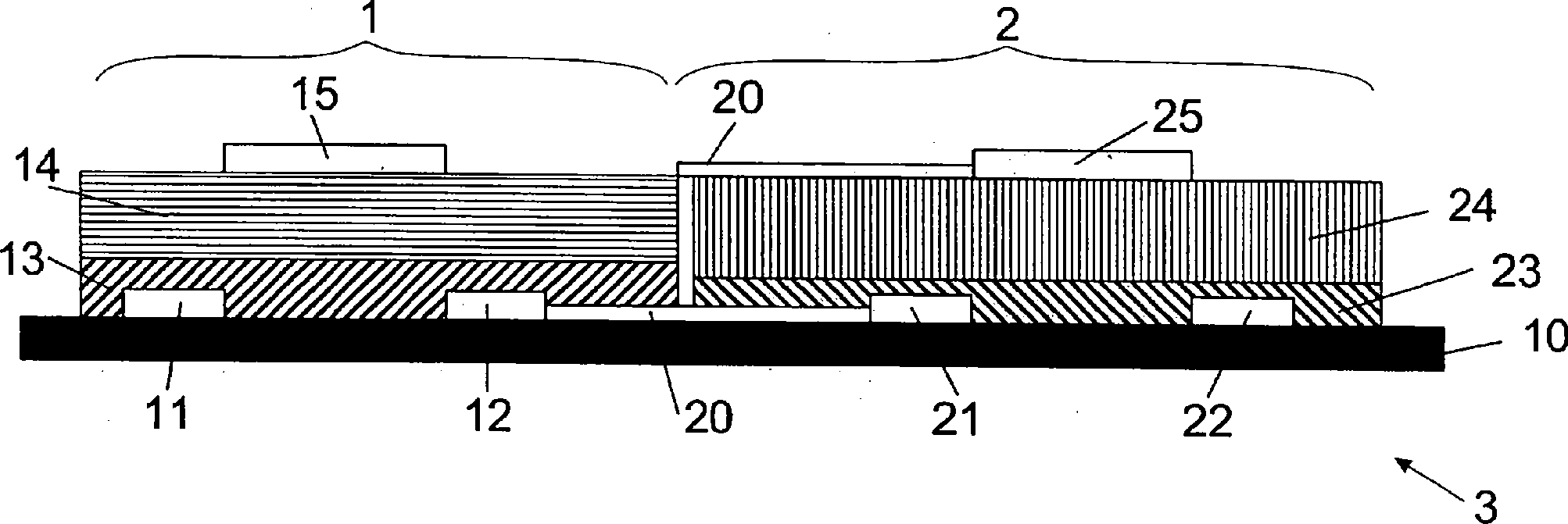
Der
erste OFET
Diese Schichten können beispielsweise durch ein Druckverfahren bereits partiell oder musterförmig strukturiert aufgebracht werden. Dazu ist vorgesehen, insbesondere die Halbleiterschicht aus einer Flüssigkeit heraus aufzubringen. Der Begriff Flüssigkeit umfaßt dabei beispielsweise Suspensionen, Emulsionen, sonstige Dispersionen oder auch Lösungen. Für die Herstellung von Lösungen sind die für die Schichten vorgesehenen organischen Materialien als lösbare Polymere ausgebildet, wobei der Begriff des Polymers hierbei, wie weiter oben bereits beschrieben, auch Oligomere und „small moleculs" sowie Nano-Partikel einschließt. Bei dem organischen Halbleiter kann es sich beispielsweise um Pentacen handeln. Es können mehrere Parameter der Flüssigkeit variiert werden:
- – die Viskosität der Flüssigkeit, sie bestimmt das Druckverhalten;
- – die Polymerkonzentration der druckfertigen Mischung, sie bestimmt die Schichtdicke;
- – die Siedetemperatur der Flüssigkeit, sie bestimmt, welches Druckverfahren einsetzbar ist;
- – die Oberflächenspannung der druckfertigen Mischung, sie bestimmt die Benetzungsfähigkeit des Trägersubstrats oder anderer Schichten.
- - the viscosity of the liquid, it determines the pressure behavior;
- The polymer concentration of the ready-to-print mixture determines the layer thickness;
- - The boiling temperature of the liquid, it determines which printing process can be used;
- The surface tension of the ready-to-print mixture determines the wettability of the support substrate or other layers.
Es kann auch vorgesehen sein, wie weiter vorstehend ausführlich beschrieben, die Schichten durch mehrmalig aufeinanderfolgendes Drucken mit variabler Schichtdicke auszubilden.It may also be provided, as further described in detail above, the layers by successively printing with variable Form layer thickness.
Es
kann auch vorgesehen sein, auf das Substrat
Die
Elektroden
Die
Elektroden
Bei
den Elektroden
Der
zweite OFET
In
Weiter
ist es auch möglich,
dass die Gate-Elektrode
In
In
diesen Ausführungsbeispielen
gemäß
Wie
in
Wenn
beide organischen Halbleiterschichten
Die
Bei dem dargestellten Ausführungsbeispiel kann vorzugsweise vorgesehen sein, daß die jeweils in einer Ebene angeordneten Elektroden aus gleichem Material ausgebildet sind, beispielsweise aus einer leitfähigen Druckfarbe oder aus einer aufgesputterten, galvanisierten oder aufgedampften Metallschicht. Es kann aber auch vorgesehen sein, daß sie aus jeweils unterschiedlichen Materialien ausgebildet sind, vorzugsweise, wenn damit ein vorteilhafter funktioneller Effekt verbunden ist.at the illustrated embodiment can preferably be provided that each in a plane arranged electrodes are formed of the same material, for example, from a conductive Printing ink or from a sputtered, galvanized or vapor-deposited Metal layer. But it can also be provided that they out each different materials are formed, preferably, if this is associated with an advantageous functional effect.
In
dem in
Die
mit dem in
Es
kann vorgesehen sein, daß die
beiden OFET
Das
Grundschaltbild des in
Die
beiden Drain-Elektroden
Die
Source-Elektrode
Die
beiden Drain-Elektroden
Es
kann aber auch vorgesehen sein, daß die vorstehend beschriebene
Anordnung so ausgebildet ist, daß die gemeinsame Gate-Elektrode
Wegen der vorstehend beschriebenen Möglichkeit, die Anordnung der das Logik-Gatter bildenden Schichten um 180° zu drehen, kann eine besonders vorteilhafte Topologie miteinander verschalteter Logik-Gatter oder anderer Bauelemente ausgebildet sein und auf diese Weise beispielsweise Durchkontaktierungen zur Verbindung der Logik-Gatter bzw. Bauelemente vermieden bzw. in ihrer Anzahl minimiert sein.Because of the possibility described above, to rotate the arrangement of the logic gate forming layers 180 °, can be a particularly advantageous topology interconnected logic gates or other components may be formed and in this way, for example Through-contacts for connecting the logic gates or components be avoided or minimized in number.
Die
Die
beiden OFET
Das
Strom-Spannungs-Diagramm in
In
Die
Durch die Ausbildung der erfindungsgemäßen Logik-Gatter mit unterschiedlichen Feldeffekttransistoren, die durch schichtweises Drucken und/oder Rakeln herstellbar sind, ist die kostengünstige Massenproduktion der erfindungsgemäßen Logik-Gatter ermöglicht. Die Druckverfahren haben einen solchen Stand erreicht, daß feinste Strukturen in den einzelnen Schichten ausbildbar sind, die mit anderen Verfahren nur mit hohem Aufwand ausbildbar sind.Due to the design of the logic gates according to the invention with different field effect Transistors which can be produced by layer-by-layer printing and / or doctoring enable cost-effective mass production of the logic gates according to the invention. The printing methods have reached such a level that finest structures in the individual layers can be formed, which can be formed with other methods only with great effort.
Claims (27)
Priority Applications (11)
| Application Number | Priority Date | Filing Date | Title |
|---|---|---|---|
| DE102004059467A DE102004059467A1 (en) | 2004-12-10 | 2004-12-10 | Gate made of organic field effect transistors |
| EP05850139A EP1825516A2 (en) | 2004-12-10 | 2005-12-06 | Organic field effect transistor gate |
| PCT/DE2005/002195 WO2006061000A2 (en) | 2004-12-10 | 2005-12-06 | Organic field effect transistor gate |
| AU2005313714A AU2005313714A1 (en) | 2004-12-10 | 2005-12-06 | Organic field effect transistor gate |
| CA002595114A CA2595114A1 (en) | 2004-12-10 | 2005-12-06 | Organic field effect transistor gate |
| JP2007544729A JP2008523595A (en) | 2004-12-10 | 2005-12-06 | Organic field effect transistor gate |
| US11/721,244 US20080197343A1 (en) | 2004-12-10 | 2005-12-06 | Organic Field Effect Transistor Gate |
| MX2007006725A MX2007006725A (en) | 2004-12-10 | 2005-12-06 | Organic field effect transistor gate. |
| KR1020077013005A KR20070085953A (en) | 2004-12-10 | 2005-12-06 | Organic field effect transistor gate |
| CNA200580042446XA CN101076893A (en) | 2004-12-10 | 2005-12-06 | Organic field effect transistor gate |
| TW094143111A TWI333701B (en) | 2004-12-10 | 2005-12-07 | Gatter aus organischen feldeffekttransistoren |
Applications Claiming Priority (1)
| Application Number | Priority Date | Filing Date | Title |
|---|---|---|---|
| DE102004059467A DE102004059467A1 (en) | 2004-12-10 | 2004-12-10 | Gate made of organic field effect transistors |
Publications (1)
| Publication Number | Publication Date |
|---|---|
| DE102004059467A1 true DE102004059467A1 (en) | 2006-07-20 |
Family
ID=36578264
Family Applications (1)
| Application Number | Title | Priority Date | Filing Date |
|---|---|---|---|
| DE102004059467A Ceased DE102004059467A1 (en) | 2004-12-10 | 2004-12-10 | Gate made of organic field effect transistors |
Country Status (11)
| Country | Link |
|---|---|
| US (1) | US20080197343A1 (en) |
| EP (1) | EP1825516A2 (en) |
| JP (1) | JP2008523595A (en) |
| KR (1) | KR20070085953A (en) |
| CN (1) | CN101076893A (en) |
| AU (1) | AU2005313714A1 (en) |
| CA (1) | CA2595114A1 (en) |
| DE (1) | DE102004059467A1 (en) |
| MX (1) | MX2007006725A (en) |
| TW (1) | TWI333701B (en) |
| WO (1) | WO2006061000A2 (en) |
Cited By (2)
| Publication number | Priority date | Publication date | Assignee | Title |
|---|---|---|---|---|
| DE102006037433A1 (en) * | 2006-08-09 | 2008-02-28 | Ovd Kinegram Ag | Method for producing at least one multilayer body and multilayer body |
| DE102009012302A1 (en) * | 2009-03-11 | 2010-09-23 | Polyic Gmbh & Co. Kg | Organic electronic component i.e. parallel-series converter, for converting parallel input signal of N bit into serial output signal, has output electrically connected with electrode that is arranged on surface of semiconductor layer |
Families Citing this family (16)
| Publication number | Priority date | Publication date | Assignee | Title |
|---|---|---|---|---|
| WO2004102395A1 (en) | 2003-05-16 | 2004-11-25 | Japan-Wave Inc. | System for preventing unauthorized use of digital content |
| JP2008010566A (en) * | 2006-06-28 | 2008-01-17 | Ricoh Co Ltd | Semiconductor device |
| KR100790761B1 (en) * | 2006-09-29 | 2008-01-03 | 한국전자통신연구원 | Inverter |
| JP5104057B2 (en) * | 2007-06-21 | 2012-12-19 | セイコーエプソン株式会社 | Manufacturing method of semiconductor device |
| US20090004368A1 (en) * | 2007-06-29 | 2009-01-01 | Weyerhaeuser Co. | Systems and methods for curing a deposited layer on a substrate |
| TWI412125B (en) * | 2007-07-17 | 2013-10-11 | Creator Technology Bv | Method of manufacturing electronic components and electronic components |
| US20090165056A1 (en) * | 2007-12-19 | 2009-06-25 | General Instrument Corporation | Method and apparatus for scheduling a recording of an upcoming sdv program deliverable over a content delivery system |
| US7888169B2 (en) * | 2007-12-26 | 2011-02-15 | Organicid, Inc. | Organic semiconductor device and method of manufacturing the same |
| US7704786B2 (en) | 2007-12-26 | 2010-04-27 | Organicid Inc. | Printed organic logic circuits using a floating gate transistor as a load device |
| US8463116B2 (en) | 2008-07-01 | 2013-06-11 | Tap Development Limited Liability Company | Systems for curing deposited material using feedback control |
| JP2010034343A (en) * | 2008-07-30 | 2010-02-12 | Sumitomo Chemical Co Ltd | Method for manufacturing semiconductor device and semiconductor device |
| JP5548976B2 (en) * | 2009-06-25 | 2014-07-16 | セイコーエプソン株式会社 | Semiconductor device |
| JP5558222B2 (en) * | 2010-06-18 | 2014-07-23 | シャープ株式会社 | Method for manufacturing thin film transistor substrate |
| CN107104188A (en) * | 2017-04-20 | 2017-08-29 | 上海幂方电子科技有限公司 | The preparation method of organic complementary type NOT gate device |
| CN109920922B (en) * | 2017-12-12 | 2020-07-17 | 京东方科技集团股份有限公司 | Organic light-emitting device and preparation method thereof, display substrate, and display driving method |
| CN113130661A (en) * | 2021-04-19 | 2021-07-16 | 湖南大学 | An unshielded tri-gate transistor device and a resistive full-swing inverter based thereon |
Citations (1)
| Publication number | Priority date | Publication date | Assignee | Title |
|---|---|---|---|---|
| US20040063267A1 (en) * | 2000-12-08 | 2004-04-01 | Adolf Bernds | Organic field-effect transistor, method for structuring and ofet and integrated circuit |
Family Cites Families (107)
| Publication number | Priority date | Publication date | Assignee | Title |
|---|---|---|---|---|
| US3512052A (en) * | 1968-01-11 | 1970-05-12 | Gen Motors Corp | Metal-insulator-semiconductor voltage variable capacitor with controlled resistivity dielectric |
| US3769096A (en) * | 1971-03-12 | 1973-10-30 | Bell Telephone Labor Inc | Pyroelectric devices |
| JPS543594B2 (en) * | 1973-10-12 | 1979-02-24 | ||
| JPS54101176A (en) * | 1978-01-26 | 1979-08-09 | Shinetsu Polymer Co | Contact member for push switch |
| US4442019A (en) * | 1978-05-26 | 1984-04-10 | Marks Alvin M | Electroordered dipole suspension |
| US4246298A (en) * | 1979-03-14 | 1981-01-20 | American Can Company | Rapid curing of epoxy resin coating compositions by combination of photoinitiation and controlled heat application |
| US4340057A (en) * | 1980-12-24 | 1982-07-20 | S. C. Johnson & Son, Inc. | Radiation induced graft polymerization |
| US4554229A (en) * | 1984-04-06 | 1985-11-19 | At&T Technologies, Inc. | Multilayer hybrid integrated circuit |
| US4926052A (en) * | 1986-03-03 | 1990-05-15 | Kabushiki Kaisha Toshiba | Radiation detecting device |
| GB2215307B (en) * | 1988-03-04 | 1991-10-09 | Unisys Corp | Electronic component transportation container |
| US5364735A (en) * | 1988-07-01 | 1994-11-15 | Sony Corporation | Multiple layer optical record medium with protective layers and method for producing same |
| US4937119A (en) * | 1988-12-15 | 1990-06-26 | Hoechst Celanese Corp. | Textured organic optical data storage media and methods of preparation |
| US5892244A (en) * | 1989-01-10 | 1999-04-06 | Mitsubishi Denki Kabushiki Kaisha | Field effect transistor including πconjugate polymer and liquid crystal display including the field effect transistor |
| US6331356B1 (en) * | 1989-05-26 | 2001-12-18 | International Business Machines Corporation | Patterns of electrically conducting polymers and their application as electrodes or electrical contacts |
| US5206525A (en) * | 1989-12-27 | 1993-04-27 | Nippon Petrochemicals Co., Ltd. | Electric element capable of controlling the electric conductivity of π-conjugated macromolecular materials |
| FR2664430B1 (en) * | 1990-07-04 | 1992-09-18 | Centre Nat Rech Scient | THIN FILM FIELD EFFECT TRANSISTOR WITH MIS STRUCTURE, IN WHICH THE INSULATION AND THE SEMICONDUCTOR ARE MADE OF ORGANIC MATERIALS. |
| FR2673041A1 (en) * | 1991-02-19 | 1992-08-21 | Gemplus Card Int | METHOD FOR MANUFACTURING INTEGRATED CIRCUIT MICROMODULES AND CORRESPONDING MICROMODULE. |
| US5408109A (en) * | 1991-02-27 | 1995-04-18 | The Regents Of The University Of California | Visible light emitting diodes fabricated from soluble semiconducting polymers |
| JP3522771B2 (en) * | 1991-03-22 | 2004-04-26 | 三菱電機株式会社 | Inverter |
| US5189787A (en) * | 1991-07-30 | 1993-03-02 | Hewlett-Packard Company | Attachment of a flexible circuit to an ink-jet pen |
| JPH0580530A (en) * | 1991-09-24 | 1993-04-02 | Hitachi Ltd | Production of thin film pattern |
| EP0610183B1 (en) * | 1991-10-30 | 1995-05-10 | Fraunhofer-Gesellschaft Zur Förderung Der Angewandten Forschung E.V. | Exposure device |
| JP2709223B2 (en) * | 1992-01-30 | 1998-02-04 | 三菱電機株式会社 | Non-contact portable storage device |
| JP3457348B2 (en) * | 1993-01-15 | 2003-10-14 | 株式会社東芝 | Method for manufacturing semiconductor device |
| FR2701117B1 (en) * | 1993-02-04 | 1995-03-10 | Asulab Sa | Electrochemical measurement system with multizone sensor, and its application to glucose measurement. |
| US5567550A (en) * | 1993-03-25 | 1996-10-22 | Texas Instruments Incorporated | Method of making a mask for making integrated circuits |
| JPH0722669A (en) * | 1993-07-01 | 1995-01-24 | Mitsubishi Electric Corp | Plastic functional element |
| JP3460863B2 (en) * | 1993-09-17 | 2003-10-27 | 三菱電機株式会社 | Method for manufacturing semiconductor device |
| FR2710413B1 (en) * | 1993-09-21 | 1995-11-03 | Asulab Sa | Measuring device for removable sensors. |
| CN1106696C (en) * | 1994-05-16 | 2003-04-23 | 皇家菲利浦电子有限公司 | Semiconductor device provided with organic semiconductor material |
| JP3246189B2 (en) * | 1994-06-28 | 2002-01-15 | 株式会社日立製作所 | Semiconductor display device |
| US5528222A (en) * | 1994-09-09 | 1996-06-18 | International Business Machines Corporation | Radio frequency circuit and memory in thin flexible package |
| US5574291A (en) * | 1994-12-09 | 1996-11-12 | Lucent Technologies Inc. | Article comprising a thin film transistor with low conductivity organic layer |
| US5630986A (en) * | 1995-01-13 | 1997-05-20 | Bayer Corporation | Dispensing instrument for fluid monitoring sensors |
| JP3068430B2 (en) * | 1995-04-25 | 2000-07-24 | 富山日本電気株式会社 | Solid electrolytic capacitor and method of manufacturing the same |
| US5652645A (en) * | 1995-07-24 | 1997-07-29 | Anvik Corporation | High-throughput, high-resolution, projection patterning system for large, flexible, roll-fed, electronic-module substrates |
| US5624199A (en) * | 1995-09-29 | 1997-04-29 | Cheng; Chin-Chang | Setting device for a joint |
| GB2310493B (en) * | 1996-02-26 | 2000-08-02 | Unilever Plc | Determination of the characteristics of fluid |
| JP3080579B2 (en) * | 1996-03-06 | 2000-08-28 | 富士機工電子株式会社 | Manufacturing method of air rear grid array package |
| DE19629656A1 (en) * | 1996-07-23 | 1998-01-29 | Boehringer Mannheim Gmbh | Diagnostic test carrier with multilayer test field and method for the determination of analyte with its aid |
| US5946551A (en) * | 1997-03-25 | 1999-08-31 | Dimitrakopoulos; Christos Dimitrios | Fabrication of thin film effect transistor comprising an organic semiconductor and chemical solution deposited metal oxide gate dielectric |
| US6344662B1 (en) * | 1997-03-25 | 2002-02-05 | International Business Machines Corporation | Thin-film field-effect transistor with organic-inorganic hybrid semiconductor requiring low operating voltages |
| KR100248392B1 (en) * | 1997-05-15 | 2000-09-01 | 정선종 | Organic Active Driving Electroluminescent Device Combined with Organic Field Effect Transistor and Fabrication Method |
| JP4509228B2 (en) * | 1997-08-22 | 2010-07-21 | コーニンクレッカ フィリップス エレクトロニクス エヌ ヴィ | Field effect transistor made of organic material and method of manufacturing the same |
| JP2001516110A (en) * | 1997-09-11 | 2001-09-25 | プレシジョン ダイナミクス コーポレイション | High frequency identification tag with flexible substrate |
| US6251513B1 (en) * | 1997-11-08 | 2001-06-26 | Littlefuse, Inc. | Polymer composites for overvoltage protection |
| WO1999030432A1 (en) * | 1997-12-05 | 1999-06-17 | Koninklijke Philips Electronics N.V. | Identification transponder |
| US6083104A (en) * | 1998-01-16 | 2000-07-04 | Silverlit Toys (U.S.A.), Inc. | Programmable toy with an independent game cartridge |
| JP2002515641A (en) * | 1998-01-28 | 2002-05-28 | シン フイルム エレクトロニクス エイエスエイ | Method for producing three-dimensional conductive or semiconductive structure and method for erasing this structure |
| US6087196A (en) * | 1998-01-30 | 2000-07-11 | The Trustees Of Princeton University | Fabrication of organic semiconductor devices using ink jet printing |
| US6045977A (en) * | 1998-02-19 | 2000-04-04 | Lucent Technologies Inc. | Process for patterning conductive polyaniline films |
| WO1999053371A1 (en) * | 1998-04-10 | 1999-10-21 | E-Ink Corporation | Electronic displays using organic-based field effect transistors |
| GB9808061D0 (en) * | 1998-04-16 | 1998-06-17 | Cambridge Display Tech Ltd | Polymer devices |
| TW410478B (en) * | 1998-05-29 | 2000-11-01 | Lucent Technologies Inc | Thin-film transistor monolithically integrated with an organic light-emitting diode |
| US5967048A (en) * | 1998-06-12 | 1999-10-19 | Howard A. Fromson | Method and apparatus for the multiple imaging of a continuous web |
| CN1312958A (en) * | 1998-06-19 | 2001-09-12 | 薄膜电子有限公司 | An integrated inorganic/organic complementary thin-film transistor circuit and a method for its production |
| US6215130B1 (en) * | 1998-08-20 | 2001-04-10 | Lucent Technologies Inc. | Thin film transistors |
| US6384804B1 (en) * | 1998-11-25 | 2002-05-07 | Lucent Techonologies Inc. | Display comprising organic smart pixels |
| US6506438B2 (en) * | 1998-12-15 | 2003-01-14 | E Ink Corporation | Method for printing of transistor arrays on plastic substrates |
| US6114088A (en) * | 1999-01-15 | 2000-09-05 | 3M Innovative Properties Company | Thermal transfer element for forming multilayer devices |
| DE60003281T2 (en) * | 1999-01-15 | 2004-05-06 | 3M Innovative Properties Co., Saint Paul | Thermal transfer process. |
| GB2347013A (en) * | 1999-02-16 | 2000-08-23 | Sharp Kk | Charge-transport structures |
| ES2255768T3 (en) * | 1999-02-22 | 2006-07-01 | Nippon Steel Corporation | HIGH RESISTANCE GALVANIZED STEEL SHEET, WITH EXCELLENT ADHERENCE OF A METAL BATHROOM AND CONFORMABILITY UNDER PRESSURE AND HIGH RESISTANCE AWAY GALVANIZED STEEL SHEET AND METHOD FOR PRODUCTION. |
| US6180956B1 (en) * | 1999-03-03 | 2001-01-30 | International Business Machine Corp. | Thin film transistors with organic-inorganic hybrid materials as semiconducting channels |
| US6207472B1 (en) * | 1999-03-09 | 2001-03-27 | International Business Machines Corporation | Low temperature thin film transistor fabrication |
| US6072716A (en) * | 1999-04-14 | 2000-06-06 | Massachusetts Institute Of Technology | Memory structures and methods of making same |
| US6383664B2 (en) * | 1999-05-11 | 2002-05-07 | The Dow Chemical Company | Electroluminescent or photocell device having protective packaging |
| US6366017B1 (en) * | 1999-07-14 | 2002-04-02 | Agilent Technologies, Inc/ | Organic light emitting diodes with distributed bragg reflector |
| US6593690B1 (en) * | 1999-09-03 | 2003-07-15 | 3M Innovative Properties Company | Large area organic electronic devices having conducting polymer buffer layers and methods of making same |
| EP1085320A1 (en) * | 1999-09-13 | 2001-03-21 | Interuniversitair Micro-Elektronica Centrum Vzw | A device for detecting an analyte in a sample based on organic materials |
| US6517995B1 (en) * | 1999-09-14 | 2003-02-11 | Massachusetts Institute Of Technology | Fabrication of finely featured devices by liquid embossing |
| US6340822B1 (en) * | 1999-10-05 | 2002-01-22 | Agere Systems Guardian Corp. | Article comprising vertically nano-interconnected circuit devices and method for making the same |
| WO2001027998A1 (en) * | 1999-10-11 | 2001-04-19 | Koninklijke Philips Electronics N.V. | Integrated circuit |
| US6335539B1 (en) * | 1999-11-05 | 2002-01-01 | International Business Machines Corporation | Method for improving performance of organic semiconductors in bottom electrode structure |
| US6284562B1 (en) * | 1999-11-17 | 2001-09-04 | Agere Systems Guardian Corp. | Thin film transistors |
| US6136702A (en) * | 1999-11-29 | 2000-10-24 | Lucent Technologies Inc. | Thin film transistors |
| US6621098B1 (en) * | 1999-11-29 | 2003-09-16 | The Penn State Research Foundation | Thin-film transistor and methods of manufacturing and incorporating a semiconducting organic material |
| US6197663B1 (en) * | 1999-12-07 | 2001-03-06 | Lucent Technologies Inc. | Process for fabricating integrated circuit devices having thin film transistors |
| AU2015901A (en) * | 1999-12-21 | 2001-07-03 | Plastic Logic Limited | Inkjet-fabricated integrated circuits |
| JP2002162652A (en) * | 2000-01-31 | 2002-06-07 | Fujitsu Ltd | Sheet display device, resin spherical body, and microcapsule |
| US6706159B2 (en) * | 2000-03-02 | 2004-03-16 | Diabetes Diagnostics | Combined lancet and electrochemical analyte-testing apparatus |
| TW497120B (en) * | 2000-03-06 | 2002-08-01 | Toshiba Corp | Transistor, semiconductor device and manufacturing method of semiconductor device |
| JP3614747B2 (en) * | 2000-03-07 | 2005-01-26 | Necエレクトロニクス株式会社 | BOOST CIRCUIT, IC CARD WITH THE SAME AND ELECTRONIC DEVICE WITH THE SAME |
| DE10033112C2 (en) * | 2000-07-07 | 2002-11-14 | Siemens Ag | Process for the production and structuring of organic field-effect transistors (OFET), OFET produced thereafter and its use |
| EP1310004A2 (en) * | 2000-08-18 | 2003-05-14 | Siemens Aktiengesellschaft | Organic field-effect transistor (ofet), a production method therefor, an integrated circuit constructed from the same and their uses |
| EP1309994A2 (en) * | 2000-08-18 | 2003-05-14 | Siemens Aktiengesellschaft | Encapsulated organic-electronic component, method for producing the same and use thereof |
| DE10044842A1 (en) * | 2000-09-11 | 2002-04-04 | Siemens Ag | Organic rectifier, circuit, RFID tag and use of an organic rectifier |
| DE10045192A1 (en) * | 2000-09-13 | 2002-04-04 | Siemens Ag | Organic data storage, RFID tag with organic data storage, use of an organic data storage |
| KR20020036916A (en) * | 2000-11-11 | 2002-05-17 | 주승기 | Method of crystallizing a silicon thin film and semiconductor device fabricated thereby |
| KR100390522B1 (en) * | 2000-12-01 | 2003-07-07 | 피티플러스(주) | Method for fabricating thin film transistor including a crystalline silicone active layer |
| GB2371910A (en) * | 2001-01-31 | 2002-08-07 | Seiko Epson Corp | Display devices |
| JP2003089259A (en) * | 2001-09-18 | 2003-03-25 | Hitachi Ltd | Pattern forming method and pattern forming apparatus |
| US7351660B2 (en) * | 2001-09-28 | 2008-04-01 | Hrl Laboratories, Llc | Process for producing high performance interconnects |
| US6679036B2 (en) * | 2001-10-15 | 2004-01-20 | Shunchi Crankshaft Co., Ltd. | Drive gear shaft structure of a self-moving type mower |
| JP4275336B2 (en) * | 2001-11-16 | 2009-06-10 | 株式会社半導体エネルギー研究所 | Method for manufacturing semiconductor device |
| DE10212640B4 (en) * | 2002-03-21 | 2004-02-05 | Siemens Ag | Logical components made of organic field effect transistors |
| US6667215B2 (en) * | 2002-05-02 | 2003-12-23 | 3M Innovative Properties | Method of making transistors |
| US6812509B2 (en) * | 2002-06-28 | 2004-11-02 | Palo Alto Research Center Inc. | Organic ferroelectric memory cells |
| JP2004152958A (en) * | 2002-10-30 | 2004-05-27 | Pioneer Electronic Corp | Organic semiconductor device |
| US6870183B2 (en) * | 2002-11-04 | 2005-03-22 | Advanced Micro Devices, Inc. | Stacked organic memory devices and methods of operating and fabricating |
| JP4296788B2 (en) * | 2003-01-28 | 2009-07-15 | パナソニック電工株式会社 | ORGANIC FIELD EFFECT TRANSISTOR, ITS MANUFACTURING METHOD, AND INTEGRATED CIRCUIT DEVICE |
| US20060243965A1 (en) * | 2003-01-28 | 2006-11-02 | De Leeuw Dagobert M | Electronic device |
| JP4406540B2 (en) * | 2003-03-28 | 2010-01-27 | シャープ株式会社 | Thin film transistor substrate and manufacturing method thereof |
| DE10330064B3 (en) * | 2003-07-03 | 2004-12-09 | Siemens Ag | Organic logic gate has load field effect transistor with potential-free gate electrode in series with switching field effect transistor |
| GB0321383D0 (en) * | 2003-09-12 | 2003-10-15 | Plastic Logic Ltd | Polymer circuits |
| KR101307481B1 (en) * | 2004-06-04 | 2013-09-26 | 더 보오드 오브 트러스티스 오브 더 유니버시티 오브 일리노이즈 | Methods and devices for fabricating and assembling printable semiconductor elements |
| US7045814B2 (en) * | 2004-06-24 | 2006-05-16 | Lucent Technologies Inc. | OFET structures with both n- and p-type channels |
-
2004
- 2004-12-10 DE DE102004059467A patent/DE102004059467A1/en not_active Ceased
-
2005
- 2005-12-06 CA CA002595114A patent/CA2595114A1/en not_active Abandoned
- 2005-12-06 MX MX2007006725A patent/MX2007006725A/en not_active Application Discontinuation
- 2005-12-06 CN CNA200580042446XA patent/CN101076893A/en active Pending
- 2005-12-06 US US11/721,244 patent/US20080197343A1/en not_active Abandoned
- 2005-12-06 EP EP05850139A patent/EP1825516A2/en not_active Withdrawn
- 2005-12-06 JP JP2007544729A patent/JP2008523595A/en active Pending
- 2005-12-06 WO PCT/DE2005/002195 patent/WO2006061000A2/en not_active Ceased
- 2005-12-06 AU AU2005313714A patent/AU2005313714A1/en not_active Abandoned
- 2005-12-06 KR KR1020077013005A patent/KR20070085953A/en not_active Ceased
- 2005-12-07 TW TW094143111A patent/TWI333701B/en not_active IP Right Cessation
Patent Citations (1)
| Publication number | Priority date | Publication date | Assignee | Title |
|---|---|---|---|---|
| US20040063267A1 (en) * | 2000-12-08 | 2004-04-01 | Adolf Bernds | Organic field-effect transistor, method for structuring and ofet and integrated circuit |
Cited By (5)
| Publication number | Priority date | Publication date | Assignee | Title |
|---|---|---|---|---|
| DE102006037433A1 (en) * | 2006-08-09 | 2008-02-28 | Ovd Kinegram Ag | Method for producing at least one multilayer body and multilayer body |
| DE102006037433B4 (en) * | 2006-08-09 | 2010-08-19 | Ovd Kinegram Ag | Method for producing a multilayer body and multilayer body |
| US8129217B2 (en) | 2006-08-09 | 2012-03-06 | Ovd Kinegram Ag | Method for producing at least one multilayer body, and multilayer body |
| US8502213B2 (en) | 2006-08-09 | 2013-08-06 | Ovd Kinegram Ag | Method for producing at least one multilayer body, and multilayer body |
| DE102009012302A1 (en) * | 2009-03-11 | 2010-09-23 | Polyic Gmbh & Co. Kg | Organic electronic component i.e. parallel-series converter, for converting parallel input signal of N bit into serial output signal, has output electrically connected with electrode that is arranged on surface of semiconductor layer |
Also Published As
| Publication number | Publication date |
|---|---|
| AU2005313714A1 (en) | 2006-06-15 |
| MX2007006725A (en) | 2007-07-25 |
| TW200640050A (en) | 2006-11-16 |
| WO2006061000A3 (en) | 2006-08-24 |
| WO2006061000A2 (en) | 2006-06-15 |
| CA2595114A1 (en) | 2006-06-15 |
| JP2008523595A (en) | 2008-07-03 |
| EP1825516A2 (en) | 2007-08-29 |
| CN101076893A (en) | 2007-11-21 |
| KR20070085953A (en) | 2007-08-27 |
| TWI333701B (en) | 2010-11-21 |
| US20080197343A1 (en) | 2008-08-21 |
Similar Documents
| Publication | Publication Date | Title |
|---|---|---|
| DE102004059467A1 (en) | Gate made of organic field effect transistors | |
| WO2002015293A2 (en) | Organic field-effect transistor (ofet), a production method therefor, an integrated circuit constructed from the same and their uses | |
| EP2087519B1 (en) | Field effect transistor, and electric circuit | |
| EP1656683B1 (en) | Organic capacitor having a voltage-controlled capacitance | |
| DE102011004195A1 (en) | Thin-film transistor structure, process for its manufacture, and electronic device | |
| DE10212926A1 (en) | Semiconductor storage cell has a modulation region arranged between a first gate electrode of a gate electrode arrangement and an insulating region | |
| DE10209400A1 (en) | Transponder circuit for a transponder has a rectifier circuit with a component that has a coating of organic material | |
| DE3722941C2 (en) | ||
| DE2124635A1 (en) | Method for controlling an area of high electric field strength in semiconductors | |
| DE2228931C2 (en) | Integrated semiconductor arrangement with at least one material-different semiconductor junction and method for operation | |
| DE102005017655B4 (en) | Multilayer composite body with electronic function | |
| EP1925033A1 (en) | Electronic circuit and method for the manufacture of the same | |
| EP1704606B1 (en) | Method for the production of an organic transistor comprising a self-adjusting gate electrode | |
| EP1999757B1 (en) | Method for programming an electronic circuit and electronic circuit | |
| EP1922774B1 (en) | Organic component and electric circuit comprising said component | |
| DE102021105680B3 (en) | Semiconductor device and method of forming a semiconductor device | |
| DE112004002925B4 (en) | logic circuit | |
| DE102005035590A1 (en) | Electronic component has flexible substrate and stack of layers including function layer on substratesurface | |
| DE10057502A1 (en) | Organic field effect transistor has at least two current channels and/or one vertical current channel transverse to surface of substrate formed by field effect when voltage applied | |
| DE202005017580U1 (en) | Nanoelectronic structural element comprising two electrically conducting contacts bridged over by molecular monlayer useful in microelectronics has current/voltage characteristic with region of negative differential resistance |
Legal Events
| Date | Code | Title | Description |
|---|---|---|---|
| OP8 | Request for examination as to paragraph 44 patent law | ||
| 8127 | New person/name/address of the applicant |
Owner name: POLYIC GMBH & CO.KG, 90763 FUERTH, DE |
|
| R016 | Response to examination communication | ||
| R002 | Refusal decision in examination/registration proceedings | ||
| R003 | Refusal decision now final |
Effective date: 20131017 |