DE102004041626B4 - Chip card, and chip card security device - Google Patents
Chip card, and chip card security device Download PDFInfo
- Publication number
- DE102004041626B4 DE102004041626B4 DE102004041626A DE102004041626A DE102004041626B4 DE 102004041626 B4 DE102004041626 B4 DE 102004041626B4 DE 102004041626 A DE102004041626 A DE 102004041626A DE 102004041626 A DE102004041626 A DE 102004041626A DE 102004041626 B4 DE102004041626 B4 DE 102004041626B4
- Authority
- DE
- Germany
- Prior art keywords
- chip card
- memory
- security device
- chip
- state
- Prior art date
- Legal status (The legal status is an assumption and is not a legal conclusion. Google has not performed a legal analysis and makes no representation as to the accuracy of the status listed.)
- Expired - Fee Related
Links
Classifications
-
- G—PHYSICS
- G06—COMPUTING OR CALCULATING; COUNTING
- G06K—GRAPHICAL DATA READING; PRESENTATION OF DATA; RECORD CARRIERS; HANDLING RECORD CARRIERS
- G06K19/00—Record carriers for use with machines and with at least a part designed to carry digital markings
- G06K19/06—Record carriers for use with machines and with at least a part designed to carry digital markings characterised by the kind of the digital marking, e.g. shape, nature, code
- G06K19/067—Record carriers with conductive marks, printed circuits or semiconductor circuit elements, e.g. credit or identity cards also with resonating or responding marks without active components
- G06K19/07—Record carriers with conductive marks, printed circuits or semiconductor circuit elements, e.g. credit or identity cards also with resonating or responding marks without active components with integrated circuit chips
- G06K19/073—Special arrangements for circuits, e.g. for protecting identification code in memory
- G06K19/07309—Means for preventing undesired reading or writing from or onto record carriers
- G06K19/07372—Means for preventing undesired reading or writing from or onto record carriers by detecting tampering with the circuit
- G06K19/07381—Means for preventing undesired reading or writing from or onto record carriers by detecting tampering with the circuit with deactivation or otherwise incapacitation of at least a part of the circuit upon detected tampering
-
- G—PHYSICS
- G11—INFORMATION STORAGE
- G11C—STATIC STORES
- G11C13/00—Digital stores characterised by the use of storage elements not covered by groups G11C11/00, G11C23/00, or G11C25/00
- G11C13/0002—Digital stores characterised by the use of storage elements not covered by groups G11C11/00, G11C23/00, or G11C25/00 using resistive RAM [RRAM] elements
- G11C13/0004—Digital stores characterised by the use of storage elements not covered by groups G11C11/00, G11C23/00, or G11C25/00 using resistive RAM [RRAM] elements comprising amorphous/crystalline phase transition cells
-
- G—PHYSICS
- G11—INFORMATION STORAGE
- G11C—STATIC STORES
- G11C13/00—Digital stores characterised by the use of storage elements not covered by groups G11C11/00, G11C23/00, or G11C25/00
- G11C13/0002—Digital stores characterised by the use of storage elements not covered by groups G11C11/00, G11C23/00, or G11C25/00 using resistive RAM [RRAM] elements
- G11C13/0009—RRAM elements whose operation depends upon chemical change
- G11C13/0011—RRAM elements whose operation depends upon chemical change comprising conductive bridging RAM [CBRAM] or programming metallization cells [PMCs]
-
- G—PHYSICS
- G11—INFORMATION STORAGE
- G11C—STATIC STORES
- G11C13/00—Digital stores characterised by the use of storage elements not covered by groups G11C11/00, G11C23/00, or G11C25/00
- G11C13/0002—Digital stores characterised by the use of storage elements not covered by groups G11C11/00, G11C23/00, or G11C25/00 using resistive RAM [RRAM] elements
- G11C13/0021—Auxiliary circuits
- G11C13/0059—Security or protection circuits or methods
-
- H10W42/405—
-
- G—PHYSICS
- G11—INFORMATION STORAGE
- G11C—STATIC STORES
- G11C13/00—Digital stores characterised by the use of storage elements not covered by groups G11C11/00, G11C23/00, or G11C25/00
- G11C13/04—Digital stores characterised by the use of storage elements not covered by groups G11C11/00, G11C23/00, or G11C25/00 using optical elements ; using other beam accessed elements, e.g. electron or ion beam
-
- G—PHYSICS
- G11—INFORMATION STORAGE
- G11C—STATIC STORES
- G11C2213/00—Indexing scheme relating to G11C13/00 for features not covered by this group
- G11C2213/70—Resistive array aspects
- G11C2213/79—Array wherein the access device being a transistor
Landscapes
- Engineering & Computer Science (AREA)
- Computer Security & Cryptography (AREA)
- Computer Hardware Design (AREA)
- Chemical & Material Sciences (AREA)
- Crystallography & Structural Chemistry (AREA)
- General Engineering & Computer Science (AREA)
- Microelectronics & Electronic Packaging (AREA)
- Physics & Mathematics (AREA)
- General Physics & Mathematics (AREA)
- Theoretical Computer Science (AREA)
- Storage Device Security (AREA)
- Read Only Memory (AREA)
Abstract
Chipkarte
(1), dadurch gekennzeichnet, dass die Chipkarte aufweist:
mindestens
ein Speicherbauelement (11), welches eine aktive Material-Schicht
(13) aufweist, welche durch entsprechende Schaltvorgänge in einen
mehr oder weniger leitfähigen
und/oder eine mehr oder weniger hohe Kapazität aufweisenden Zustand versetzbar
ist, wobei die Chipkarte (1) des weiteren eine Chipkarten-Sicherungs-Einrichtung
(11, 30; 11, 40) aufweist, und das Speicherbauelement (11) Teil der
Chipkarten-Sicherungs-Einrichtung (11, 30; 11, 40) ist.Chip card (1), characterized in that the chip card comprises:
at least one memory component (11), which has an active material layer (13), which can be offset by corresponding switching operations in a more or less conductive and / or a more or less high-capacitance state, wherein the chip card (1) further a chip card security device (11, 30, 11, 40), and the memory component (11) is part of the chip card security device (11, 30, 11, 40).
Description
Die Erfindung betrifft eine Chipkarte, insbesondere eine Chipkarte mit Sicherungs-Einrichtung, eine Chipkarten-Sicherungs-Einrichtung, sowie ein Verfahren zur Verwendung bei der Sicherung einer Chipkarte.The The invention relates to a chip card, in particular a chip card with Security device, a smart card security device, and a method for use in securing a smart card.
Eine Chipkarte bzw. Smart Card ist eine einen oder mehrere Chips aufweisende, programmierbare Kunststoff-Karte z.B. für den bargeldlosen Geldverkehr (z.B. zur Verwendung als Kreditkarte, EC-Karte, Telefonkarte, „electronic cash"-Karte, etc.), zur Bedienung von Zugangskontrollsystemen, zur Freischaltung von Pay-TV, zur Speicherung von Patientendaten, zur Verwendung als Mitglieds-Ausweis, etc., etc., etc.A Smart card is a one or more chips having programmable plastic card e.g. for cashless money transactions (e.g., for use as a credit card, debit card, calling card, "electronic cash "card, etc.), to Operation of access control systems, for the activation of pay-TV, for storing patient data, for use as a membership card, etc., etc., etc.
Herkömmliche Chipkarten weisen z.B. einen Mikrocontroller-Chip auf, sowie z.B. ein oder mehrere – z.B. auf demselben Chip wie der Mikrocontroller integrierte – Speicherbauelemente, insbesondere Halbleiter-Speicherbauelemente, z.B. ROM-Speicherbauelemente (ROM = Read Only Memory bzw. Festwertspeicher) – insbesondere PROMs oder EEPROMs –, und/oder RAM-Speicherbauelemente (RAM = Random Access Memory bzw. Schreib-Lese-Speicher), etc.conventional Chip cards have e.g. a microcontroller chip, as well as e.g. one or more - e.g. on the same chip as the microcontroller integrated memory devices, in particular semiconductor memory devices, e.g. ROM memory devices (ROM = Read Only Memory) - in particular PROMs or EEPROMs -, and / or RAM memory devices (RAM = Random Access Memory or read-write memory), Etc.
Der oder die auf der Chipkarte vorgesehenen Chips (bzw. die obere Chipfläche) können von einer entsprechenden Schutz-Schicht überdeckt sein.Of the or the chips (or the upper chip surface) provided on the chip card can be replaced by a corresponding protective layer covered be.
Chipkarten finden weiter zunehmende Verbreitung.smart cards continue to find increasing distribution.
Da auf einer Chipkarte – insbesondere auf deren o.g. Speicherbauelementen – häufig sicherheitsrelevante Daten gespeichert sind, sollten diese vor unberechtigtem Zugriff geschützt werden.There on a chip card - in particular on the o.g. Memory devices - often safety-relevant data stored, they should be protected against unauthorized access.
Des weiteren sollte verhindert werden, dass die Funktionsweise der Karte manipuliert werden kann.Of further, it should prevent the functioning of the card can be manipulated.
Trotz der zu den o.g. Zwecken eingesetzten Chipkarten-Sicherungs-Mechanismen konnten in der Vergangenheit immer wieder die entsprechenden Mechanismen „geknackt", und konnte – unberechtigt – auf die auf den Speicherbauelementen gespeicherten Daten zugegriffen, und/oder die Funktionsweise der Chipkarten manipuliert werden (z.B. bei Telefonkarten, Chipkarten zur Freischaltung von Pay-TV, etc.).In spite of the one to the o.g. Purposes used chip card security mechanisms could in the past again and again the corresponding mechanisms "cracked", and could - unjustifiably - on the accessed data stored on the memory devices, and / or the operation of the smart cards are manipulated (e.g. Chip cards for the activation of pay TV, etc.).
Hierzu wurden bzw. werden u.a. die folgenden Methoden verwendet:
- i) nicht invasiv: – Veränderung der Betriebsspannung/Einsatz von Spannungsspitzen, um den Mikrocontroller in einen undefinierten Zustand zu bringen; – Übertaktung des Chips (ebenfalls, um den Mikrocontroller in einen undefinierten Zustand zu bringen); Röntgenbestrahlung, um gezielt Speicherbereiche zu löschen, und Codes zurückzusetzen; – Röntgenbestrahlung, um den Aufbau des Chips zu analysieren; etc., etc.
- ii) invasiv (nach Entfernung der Chip-Schutz-Schicht, bzw. Freilegen der Chipfläche): – Optisches Auslesen der ROM-Speicherbauelemente (möglich z.B. bei Fuse-/Anti-Fuse-, und Ionenimplantations-Programmierverfahren); – Bestrahlung mit (UV-)Licht, um den Mikrocontroller in einen undefinierten Zustand zu bringen; – Abgriff von an entsprechenden Chip-Leiterbahnen anliegenden Signalen mit Hilfe von Kontakt-Nadeln, und darauffolgende Signal-Analyse; – Detektion der Chip-Spannungs-Signale mittels REM-Verfahren; etc., etc.
- i) non-invasive: - change of operating voltage / use of voltage peaks to bring the microcontroller in an undefined state; - overclocking the chip (also to bring the microcontroller into an undefined state); X-ray irradiation to selectively delete memory areas and reset codes; X-ray irradiation to analyze the structure of the chip; etc., etc.
- ii) invasive (after removal of the chip protection layer, or exposure of the chip area): - Optical readout of the ROM memory devices (possible eg in fuse / anti-fuse and ion implantation programming methods); - Irradiation with (UV) light to bring the microcontroller in an undefined state; - Tapping of signals applied to corresponding chip tracks with the help of contact needles, and subsequent signal analysis; - Detection of the chip voltage signals by means of SEM method; etc., etc.
Entsprechende Verfahren sind z.B. in J. Wagner: Leistungsfähigkeit von Chipkarten (Smart Cards), Kurs 2319, Fachbereich Nachrichtentechnik, Fernuniversität Hagen (1998) offenbart, sowie z.B. in J. Posegga: Smartcards, Summer School: „Sicherheit in Netzen und verteilten Systemen", TU Braunschweig (2003).Appropriate Methods are e.g. in J. Wagner: Performance of smart cards, Course 2319, Department of Telecommunications, University of Hagen (1998), as well as e.g. in J. Posegga: Smart Cards, Summer School: "Security in Networks and Distributed Systems ", TU Braunschweig (2003).
Zum Schutz vor unberechtigtem Chipkarten-Daten-Zugriff bzw. vor unberechtigter Chipkarten-Manipulation können z.B. entsprechende, herkömmliche Licht- und/oder Wärme-Sensoren verwendet werden, mit deren Hilfe z.B. ermittelt werden kann, dass – zur Durchführung der o.g. invasiven Chipkarten-Daten-Zugriffs- bzw. Chipkarten-Manipulations-Verfahren – die Chip-Schutz-Schicht entfernt, bzw. die Chipfläche freigelegt wurde.To the Protection against unauthorized chip card data access or against unauthorized access Chip card manipulation can e.g. corresponding, conventional Light and / or heat sensors can be used, with the help of e.g. can be determined that - to carry out the above-mentioned invasive smart card data access or chip card manipulation method - the chip protection layer removed, or the chip surface exposed has been.
Von Nachteil ist u.a., dass die Sensor-Bereiche relativ leicht zu erkennen sind, und dadurch der durch die Sensoren bereitgestellte Schutzmechanismus relativ leicht umgangen werden kann.From Disadvantage is u.a. That the sensor areas relatively easy to recognize and thereby the protection provided by the sensors can be easily bypassed.
Im Stand der Technik sind – seit neuerem – sog. „resistive" bzw. „resistiv schaltende" Speicherbauelemente bekannt, z.B. sog. Phasen-Wechsel-Speicher (Phase Change Memories), PMC-Speicher (PMC = Programmable Metallization Cell), CB-Speicher (CB = Conductive Bridging), etc.in the State of the art are - since newer - so-called "resistive" or "resistive switching "memory components known, e.g. so-called phase change memories, PMC memory (PMC = Programmable Metallization Cell), CB memory (CB = Conductive Bridging), etc.
Bei „resistiven" bzw. „resistiv schaltenden" Speicherbauelementen wird ein – z.B. zwischen zwei entsprechenden Elektroden (d.h. einer Anode, und einer Kathode) angeordnetes – „aktives" Material durch entsprechende Schaltvorgänge (genauer: durch entsprechende Strom- oder Spannungs-Pulse entsprechender Höhe und Dauer) in einen mehr oder weniger leitfähigen Zustand versetzt. Dabei entspricht z.B. der mehr leitfähige Zustand einer gespeicherten, logischen „eins", und der weniger leitfähige Zustand einer gespeicherten, logischen „null", oder umgekehrt.In the case of "resistive" or "resistively switching" memory components, an "active" material arranged, for example, between two corresponding electrodes (ie an anode and a cathode) is produced by corresponding switching processes (more precisely: by corresponding current or voltage pulses of corresponding magnitude and duration) in a more or less conductive state ent For example, the more conductive state speaks of a stored, logical "one," and the less conductive state of a stored, logical "zero," or vice versa.
Bei sog. Multilevel-Speicherverfahren kann – in Form mehrerer, verschiedener (durch entsprechende Strom- oder Spannungs-Pulse erreichter) resistiver Zustände des aktiven Materials – auch mehr als 1 Bit pro Zelle gespeichert werden (z.B. 2, 3, oder 4 Bits pro Zelle, wobei jeder resistive Zustand einer entsprechenden, zu speichernden Bit-Größe zugeordnet ist).at So-called multilevel storage method can - in the form of several, different (achieved by corresponding current or voltage pulses) more resistive conditions of the active material - too more than 1 bit per cell (e.g., 2, 3, or 4 bits) per cell, with each resistive state of a corresponding, too associated with saving bit size is).
Bei Programmable Metallization Cell (PMC-), oder Conductive Bridging (CB-)Speichern kann als – zwischen zwei entsprechende Elektroden geschaltetes – „aktives" Material z.B. ein entsprechendes Chalkogenid oder eine entsprechende Chalkogenidverbindung verwendet werden (z.B. GeSe, GeS, AgSe, CuS, etc.).at Programmable Metallization Cell (PMC), or Conductive Bridging (CB) can save as - between two corresponding electrodes - "active" material, e.g., a corresponding chalcogenide or a corresponding chalcogenide compound (e.g. GeSe, GeS, AgSe, CuS, etc.).
Bei PMC- und CB-Speichern basiert der Schalt-Vorgang darauf, dass – durch Anlegen entsprechender Strom- bzw. Spannungs-Pulse entsprechender Höhe und Dauer – in dem zwischen den zwei Elektroden angeordneten, aktiven Material Elemente eines entsprechenden Abscheide-„Clusters” (z.B. Ag oder Cu oder entsprechende Ag- bzw. Cu-Verbindungen) im Volumen immer weiter anwachsen, und/oder neue Cluster gebildet werden, bis die zwei Elektroden schließlich leitend „überbrückt", d.h. leitend miteinander verbunden sind (leitender Zustand der Zelle).at PMC and CB saving based the switching process on that - through Apply appropriate current or voltage pulses of appropriate height and duration - in the arranged between the two electrodes, active material elements of a corresponding deposition "cluster" (e.g., Ag or Cu or equivalent Ag or Cu compounds) in the volume continue to increase, and / or new clusters are formed until the two electrodes finally conductively "bridge", i.e. conductively with one another connected (conductive state of the cell).
Durch Anlegen von entsprechend inversen Strom-Pulsen kann dieser Vorgang wieder rückgängig gemacht werden, wodurch die entsprechende Zelle wieder zurück in einen nicht-leitenden Zustand gebracht werden kann.By Applying corresponding inverse current pulses can this process Undone which causes the corresponding cell back into one non-conductive state can be brought.
Aus
der
In
der
Aus
der
Die Erfindung hat zur Aufgabe, eine neuartige Chipkarte, insbesondere Chipkarte mit Sicherungs-Einrichtung, eine neuartige Chipkarten-Sicherungs-Einrichtung, sowie ein neuartiges Verfahren zur Verwendung bei der Sicherung einer Chipkarte zur Verfügung zu stellen.The Invention has the task of a novel smart card, in particular Chip card with security device, a novel smart card security device, and a novel method of use in the fuse a chip card available to deliver.
Sie erreicht dieses und weitere Ziele durch die Gegenstände der Ansprüche 1, 7 und 9.she achieves this and other goals through the objects of claims 1, 7 and 9.
Vorteilhafte Weiterbildungen der Erfindung sind in den Unteransprüchen angegeben.advantageous Further developments of the invention are specified in the subclaims.
Im folgenden wird die Erfindung anhand mehrerer Ausführungsbeispiele und der beigefügten Zeichnung näher erläutert. In der Zeichnung zeigt:in the The following is the invention with reference to several embodiments and the attached drawing explained in more detail. In the drawing shows:
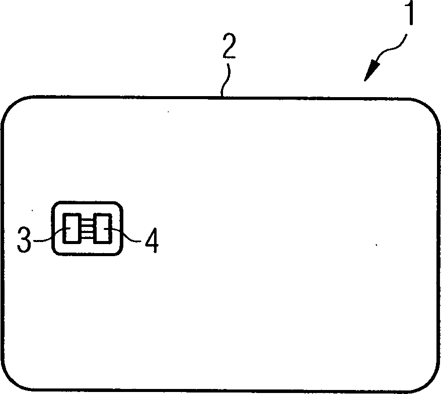
In
Diese
weist – entsprechend ähnlich wie
herkömmliche
Chipkarten – einen
Grundkörper
Die
Chipkarte
Die
Chipkarte
Die
Funktion der – bei
herkömmlichen
Chipkarten – als
Speichereinrichtung vorgesehenen Halbleiter-Speicherbauelemente, z.B. ROM-Speicherbauelemente
(ROM = Read Only Memory bzw. Festwertspeicher) – insbesondere PROMs bzw. EEPROMs –, und/oder
RAM-Speicherbauelemente (RAM = Random Access Memory bzw. Schreib-Lese-Speicher),
etc. kann – wie
im folgenden noch genauer erläutert
wird – beim
vorliegenden Ausführungsbeispiel
ganz oder teilweise von – in
der Speichereinrichtung
Bei
einer alternativen, hier nicht gezeigten Ausgestaltung sind – zusätzlich zur
die o.g. resistiv schaltenden Speicher-Zellen aufweisenden Speichereinrichtung
Der
Mikrocontroller
Die
Speichereinrichtung
Der
Mikrocontroller
Wie
bereits oben erwähnt,
sind in der Speichereinrichtung
Die
Speicher-Zellen
Zwischen
den Elektroden
Die
Material-Schicht
Bei
der Speicher-Zelle
Das
Material für
die aktive Material-Schicht
Der
Schalt-Vorgang beruht bei den Speicher-Zellen
Durch
Anlegen von entsprechend inversen Strom- bzw. Spannungs-Pulsen (z.
B. gemäß
Wie
aus
Hierzu
wird an einer mit einem Steuereingang des Transistors
Hierdurch
wird die Elektrode
Die
Leitung
Hierzu
wird an einer mit einem Steuereingang eines Transistors
Abhängig von
den Programmier-Bedingungen (d.h. der Höhe und/oder Dauer und/oder
Häufigkeit)
der an die Elektroden
Zum
Auslesen des jeweiligen Zustands der Speicher-Zelle
Hierzu
wird an einer mit einem Steuereingang eines Transistors
Je
nachdem, ob – in
Reaktion auf das Anlegen der Lese-Spannung Vread – durch
die Speicher-Zelle
Wie
bereits erwähnt,
können
einige oder mehrere der o.g. auf der Chipkarte
In
Die – als Chipkarten-Sicherungs-Einrichtung verwendete – Speicher-Zelle
Alternativ
kann die Zelle
Wie
aus
Diese
ist – über eine
Leitung
Wird – beim Versuch,
einen unberechtigten Chipkarten-Daten-Zugriff bzw. eine unberechtigte Chipkarten-Manipulation
durchzuführen – die o.g. Schutz-Schicht
beschädigt
oder entfernt, fällt
Licht auf die – z.B.
unmittelbar an der oberen Fläche
der Speichereinrichtung
Hierdurch
wird durch die Photodiode
Dies
ist möglich,
weil hierzu nur relativ geringe Schwellspannungen, beispielsweise
Spannungen zwischen lediglich +50mV und +100mV notwendig sind (vgl.
z.B. die in
Der
gleiche Effekt – Erzeugung
entsprechender Lösch-Strom- bzw. Lösch-Spannungs-Pulse durch
die Photodiode
Gegebenenfalls
kann eine zusätzliche
Konversionsschicht in der Photodiode
Beim
Betrieb der Chipkarte
Hierzu
wird eine mit der Elektrode
Zu
diesem Zweck wird an einer mit einem Steuereingang eines Transistors
Je
nachdem, ob – in
Reaktion auf das Anlegen der Lese-Spannung Vread – durch
die Speicher-Zelle
Wird
ermittelt, dass sich die Speicher-Zelle
In
Die
Speicher-Zelle
Alternativ
kann – entsprechend ähnlich wie oben
unter Bezug auf
Wie
aus
Die
Spannungs-Teiler-Einrichtung
Die
Spannungs-Teiler-Einrichtung
Die
Spannungs-Teiler-Einrichtung
Werden – beim Versuch,
einen unberechtigten Chipkarten-Daten-Zugriff bzw. eine unberechtigte Chipkarten-Manipulation
durchzuführen – relativ hohe
Spannungen bzw. entsprechende Spannungsspitzen an die Chipkarte
Beim
Betrieb der Chipkarte
Wird
ermittelt, dass sich die Speicher-Zelle
- 11
- Chipkartesmart card
- 22
- Kunststoff-GrundkörperPlastic base member
- 33
- Mikrocontrollermicrocontroller
- 44
- Speichereinrichtungmemory device
- 1111
- Speicher-ZelleMemory cell
- 12a12a
- Elektrodeelectrode
- 12b12b
- Elektrodeelectrode
- 1313
- aktive Material-Schichtactive Material layer
- 1414
- Transistortransistor
- 1515
- Steuerleitungcontrol line
- 1616
- Leitungmanagement
- 1717
- Leitungmanagement
- 1818
- Leitungmanagement
- 1919
- Leitungmanagement
- 2020
- Steuerleitungcontrol line
- 2121
- Transistortransistor
- 2222
- Leitungmanagement
- 2323
- Steuerleitungcontrol line
- 2424
- Transistortransistor
- 3030
- Photodiodephotodiode
- 3131
- Leitungmanagement
- 3232
- Leitungmanagement
- 3333
- Steuerleitungcontrol line
- 3434
- Transistortransistor
- 3838
- Leitungmanagement
- 4040
- Spannungs-Teiler-EinrichtungVoltage divider means
- 4141
- Leitungmanagement
- 4242
- Leitungmanagement
- 4242
- Leitungmanagement
Claims (9)
Priority Applications (2)
| Application Number | Priority Date | Filing Date | Title |
|---|---|---|---|
| DE102004041626A DE102004041626B4 (en) | 2004-08-27 | 2004-08-27 | Chip card, and chip card security device |
| US11/211,085 US7384002B2 (en) | 2004-08-27 | 2005-08-25 | Chip card and chip card security device |
Applications Claiming Priority (1)
| Application Number | Priority Date | Filing Date | Title |
|---|---|---|---|
| DE102004041626A DE102004041626B4 (en) | 2004-08-27 | 2004-08-27 | Chip card, and chip card security device |
Publications (2)
| Publication Number | Publication Date |
|---|---|
| DE102004041626A1 DE102004041626A1 (en) | 2006-03-09 |
| DE102004041626B4 true DE102004041626B4 (en) | 2008-06-05 |
Family
ID=35852370
Family Applications (1)
| Application Number | Title | Priority Date | Filing Date |
|---|---|---|---|
| DE102004041626A Expired - Fee Related DE102004041626B4 (en) | 2004-08-27 | 2004-08-27 | Chip card, and chip card security device |
Country Status (2)
| Country | Link |
|---|---|
| US (1) | US7384002B2 (en) |
| DE (1) | DE102004041626B4 (en) |
Families Citing this family (9)
| Publication number | Priority date | Publication date | Assignee | Title |
|---|---|---|---|---|
| WO2008132701A1 (en) * | 2007-05-01 | 2008-11-06 | Interuniversitair Microelektronica Centrum Vzw | Non-volatile memory device |
| DE102007058003B4 (en) * | 2007-12-03 | 2019-12-05 | Infineon Technologies Ag | Semiconductor device, sensor element, use of a semiconductor device and methods for the defense against light attacks |
| US7982488B2 (en) * | 2009-05-29 | 2011-07-19 | Infineon Technologies Ag | Phase-change memory security device |
| US20110002161A1 (en) * | 2009-07-06 | 2011-01-06 | Seagate Technology Llc | Phase change memory cell with selecting element |
| US8159857B2 (en) | 2009-09-21 | 2012-04-17 | Infineon Technologies Ag | Electronic device with a programmable resistive element and a method for blocking a device |
| US9105344B2 (en) * | 2012-12-20 | 2015-08-11 | Intel Corporation | Shut-off mechanism in an integrated circuit device |
| FR3031836B1 (en) * | 2015-01-15 | 2018-02-09 | Commissariat A L'energie Atomique Et Aux Energies Alternatives | ELECTRONIC CHIP PROVIDED WITH A PHASE CHANGE MATERIAL PROTECTION DEVICE, A METHOD OF DETECTING A CHIP ATTACK, AND A METHOD OF MANUFACTURING THE CHIP. |
| US9891183B2 (en) | 2015-07-07 | 2018-02-13 | Nxp B.V. | Breach sensor |
| US11674829B2 (en) | 2019-12-23 | 2023-06-13 | Palo Alto Research Center Incorporated | Low-power sensor memory |
Citations (3)
| Publication number | Priority date | Publication date | Assignee | Title |
|---|---|---|---|---|
| US20030186481A1 (en) * | 2002-03-28 | 2003-10-02 | Macronix International Co., Ltd. | Self-aligned, programmable phase change memory |
| DE10323414A1 (en) * | 2003-05-23 | 2004-12-23 | Infineon Technologies Ag | Solid state electrolyte memory cell has barrier layer between ion conductive material of variable resistance and the cathode |
| DE102004018715B3 (en) * | 2004-04-17 | 2005-11-17 | Infineon Technologies Ag | Memory cell for storing information, memory circuit and method for producing a memory cell |
Family Cites Families (9)
| Publication number | Priority date | Publication date | Assignee | Title |
|---|---|---|---|---|
| DE19610070A1 (en) * | 1996-03-14 | 1997-09-18 | Siemens Ag | Smart card |
| US5761115A (en) * | 1996-05-30 | 1998-06-02 | Axon Technologies Corporation | Programmable metallization cell structure and method of making same |
| US7446030B2 (en) * | 1999-08-27 | 2008-11-04 | Shocking Technologies, Inc. | Methods for fabricating current-carrying structures using voltage switchable dielectric materials |
| DE19955775C2 (en) * | 1999-11-19 | 2002-04-18 | Infineon Technologies Ag | Arrangement for supplying power to an electronic circuit |
| US6734455B2 (en) * | 2001-03-15 | 2004-05-11 | Micron Technology, Inc. | Agglomeration elimination for metal sputter deposition of chalcogenides |
| DE10212962B4 (en) * | 2002-03-22 | 2007-11-29 | Qimonda Ag | Semiconductor memory cell with access transistor based on an organic semiconductor material and semiconductor memory device |
| US7018863B2 (en) * | 2002-08-22 | 2006-03-28 | Micron Technology, Inc. | Method of manufacture of a resistance variable memory cell |
| KR100528464B1 (en) * | 2003-02-06 | 2005-11-15 | 삼성전자주식회사 | Security system of smart card |
| DE10314601B4 (en) * | 2003-03-31 | 2005-04-21 | Infineon Technologies Ag | Semiconductor circuit with a protection circuit against reverse polarity or overvoltage or undervoltage at the output |
-
2004
- 2004-08-27 DE DE102004041626A patent/DE102004041626B4/en not_active Expired - Fee Related
-
2005
- 2005-08-25 US US11/211,085 patent/US7384002B2/en not_active Expired - Lifetime
Patent Citations (3)
| Publication number | Priority date | Publication date | Assignee | Title |
|---|---|---|---|---|
| US20030186481A1 (en) * | 2002-03-28 | 2003-10-02 | Macronix International Co., Ltd. | Self-aligned, programmable phase change memory |
| DE10323414A1 (en) * | 2003-05-23 | 2004-12-23 | Infineon Technologies Ag | Solid state electrolyte memory cell has barrier layer between ion conductive material of variable resistance and the cathode |
| DE102004018715B3 (en) * | 2004-04-17 | 2005-11-17 | Infineon Technologies Ag | Memory cell for storing information, memory circuit and method for producing a memory cell |
Also Published As
| Publication number | Publication date |
|---|---|
| DE102004041626A1 (en) | 2006-03-09 |
| US7384002B2 (en) | 2008-06-10 |
| US20060076413A1 (en) | 2006-04-13 |
Similar Documents
| Publication | Publication Date | Title |
|---|---|---|
| DE69825923T2 (en) | Programmable aggregating sub-surface metallization structure | |
| DE69734007T2 (en) | STRUCTURE FOR PROGRAMMABLE METALLIZING CELL AND METHOD OF MANUFACTURING THEREOF | |
| DE602004010744T2 (en) | A recording method for avoiding unnecessary application of a voltage to a memory element | |
| DE102005036555B4 (en) | Programming programmable resistive memory devices | |
| DE3736882C2 (en) | Method for checking the authenticity of a data carrier with an integrated circuit | |
| EP2436011B1 (en) | Memory element, stacking, memory matrix and method for operation | |
| DE102017113967A1 (en) | ADAPTIVE OPERATION OF 3-D MEMORY | |
| DE102004041626B4 (en) | Chip card, and chip card security device | |
| DE102005030661B4 (en) | A nonvolatile semiconductor memory device and method of operating and manufacturing a nonvolatile semiconductor memory device | |
| DE102004011431B4 (en) | Method for producing a non-volatile semiconductor memory | |
| DE102004015928A1 (en) | Write / erase method for resistively switching memory devices | |
| DE102005003675A1 (en) | CBRAM memory cell comprises a metallic material incorporated in or deposited on a matrix-host material, and a memory cell having a memory switching mechanism based on the variation of the metallic material | |
| DE102004061548A1 (en) | Memory cell matrix for integration of solid electrolyte memory cells has word line and plate line that are controlled by means of selection transistor and exhibits common plate electrode which is connected to common plate circuit | |
| DE102004060712A1 (en) | Data storage device | |
| DE102004018859B3 (en) | Memory storage circuit e.g. for flip flop circuit for making available video or audio data for given length of time in terminal, has memory cell with PMC resistor having solid electrolyte material with write circuit | |
| DE102005045312A1 (en) | Semiconductor store/memory, has non-volatile storage element with polymer storage element | |
| EP1835509A1 (en) | Memory cells, memory with a memory cell and method for writing data to a memory cell | |
| EP1686590A2 (en) | Integrated semiconductor memory comprising an arrangement of non-volatile storage cells and method | |
| DE102005019587B4 (en) | Fuse memory cell with improved protection against unauthorized access | |
| DE102013020517B4 (en) | Method for reading out a resistive memory cell and a memory cell for carrying out | |
| DE19756895A1 (en) | Method for safely changing a value stored in a non-volatile memory and circuit arrangement therefor | |
| DE102007022532A1 (en) | Integrated circuit, memory cell array, memory cell module and method for operating an integrated circuit | |
| DE102007032784A1 (en) | Integrated circuit, memory module, method of operating an integrated circuit, method of manufacturing an integrated circuit, and computer program | |
| DE102006046089B3 (en) | Memory element and method for operating a memory element | |
| DE102005003025B4 (en) | PMC memory circuit and method for storing a date in a PMC memory circuit |
Legal Events
| Date | Code | Title | Description |
|---|---|---|---|
| OP8 | Request for examination as to paragraph 44 patent law | ||
| 8127 | New person/name/address of the applicant |
Owner name: QIMONDA AG, 81739 MUENCHEN, DE |
|
| 8364 | No opposition during term of opposition | ||
| 8327 | Change in the person/name/address of the patent owner |
Owner name: INFINEON TECHNOLOGIES AG, 85579 NEUBIBERG, DE |
|
| R119 | Application deemed withdrawn, or ip right lapsed, due to non-payment of renewal fee |