[go: up one dir, main page]

CN2711908Y - Improved Structure of Light Emitting Diodes - Google Patents

Improved Structure of Light Emitting Diodes Download PDF

Info

Publication number
CN2711908Y
CN2711908Y CNU2004200643544U CN200420064354U CN2711908Y CN 2711908 Y CN2711908 Y CN 2711908Y CN U2004200643544 U CNU2004200643544 U CN U2004200643544U CN 200420064354 U CN200420064354 U CN 200420064354U CN 2711908 Y CN2711908 Y CN 2711908Y
Authority
CN
China
Prior art keywords
chip
light
emitting diode
fluorescent material
supporting part
Prior art date
Legal status (The legal status is an assumption and is not a legal conclusion. Google has not performed a legal analysis and makes no representation as to the accuracy of the status listed.)
Expired - Lifetime
Application number
CNU2004200643544U
Other languages
Chinese (zh)
Inventor
刘士龙
Current Assignee (The listed assignees may be inaccurate. Google has not performed a legal analysis and makes no representation or warranty as to the accuracy of the list.)
Nisshin Import & Export Co Ltd
Original Assignee
Individual
Priority date (The priority date is an assumption and is not a legal conclusion. Google has not performed a legal analysis and makes no representation as to the accuracy of the date listed.)
Filing date
Publication date
Application filed by Individual filed Critical Individual
Priority to CNU2004200643544U priority Critical patent/CN2711908Y/en
Application granted granted Critical
Publication of CN2711908Y publication Critical patent/CN2711908Y/en
Anticipated expiration legal-status Critical
Expired - Lifetime legal-status Critical Current

Links

Images

Landscapes

  • Led Device Packages (AREA)

Abstract

本实用新型发光二极管是将芯片底部埋入由荧光胶所构成的荧光材料而与承载部构成胶合,于芯片顶层以及芯片边侧与承载部的空间是覆盖有粉末状的荧光材料,以使芯片的四周围皆由荧光材料包覆,令构成一可平衡芯片顶层与边侧光线与荧光材料的波长结合,有效避免异色光圈生成的发光二极管构造。

Figure 200420064354

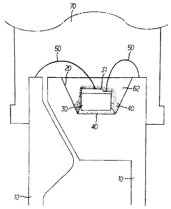
The light-emitting diode of the utility model embeds the bottom of the chip with a fluorescent material made of fluorescent glue to form a glue with the bearing part, and the space between the top layer of the chip and the side of the chip and the bearing part is covered with powdery fluorescent material, so that the chip The four sides of the chip are covered with fluorescent materials, so that a light-emitting diode structure that can balance the wavelength combination of the top layer and side of the chip and the fluorescent material can effectively avoid the generation of heterochromatic apertures.

Figure 200420064354

Description

The structure-improved of light-emitting diode
Technical field
The utility model relates to the structure-improved of light-emitting diode, aims to provide a structure that is useful in white light emitting diode especially.
Background technology
As shown in Figure 1, for the light of general using chip combines with the wavelength of fluorescent material, and then the light emitting diode construction formula that forms the existing effect of specific light color table is intended to, wherein, light-emitting diode mainly is to be provided with the supporting part 20 that is bowl cup-shaped on a conducting end 10, be beneficial to insert in the supporting part 20 chip 30 and fluorescent material 40, constitute the electrode layer 31 of chip 30 and the connection of conducting end 10 by gold thread 50 in addition.
Under the energising effect of conducting end 10, the light that chip 30 sees through fluorescent material 40 ejaculations promptly combines with the wavelength of fluorescent material 40, and form specific photochromic, for example known white light emitting diode, promptly be that the blue light that is sent with chip sees through yellow fluorescent material ejaculation, and, form the white light expression effect via combination blue, the gold-tinted ripple; Yet, in known light emitting diode construction shown in Figure 1, the last sheaf space of chip 30 main bodys is the coverings that are not subjected to fluorescent material, thereby chip 30 light that upwards light of direct projection can not the reflection of phase avris equally is subjected to the combination of fluorescent material, thereby forms tangible heterochromatic aperture easily.
So that, promptly have as shown in Figure 2, the light emitting diode construction that has suitable thickness white insulating cement 61 in chip 30 top layers covering one, it mainly is the transmission effect of wishing via white insulating cement 61, the slow expression effect that closes heterochromatic aperture, but can make the brightness of light-emitting diode reduce because of the obstruction of white insulating cement 61.Moreover, as shown in Figure 3, be to utilize Powdered fluorescent material 40 and 62 raw materials mixed of transparent adhesive tape to be poured in the space of chip 30 tops for one, with when the LED baking molding, make powdery fluorescent material 40 be deposited in the bottom surface of chip 30 top layers and supporting part 20, with the tangible heterochromatic aperture of improvement script, but the survey of the limit of its chip 30 is the effect that can't be subjected to fluorescent material 40 equally, and dimly still some is that aperture forms.
The utility model content
The purpose of this utility model provides a structure that is useful in white light emitting diode especially.
The improvement of the utility model light-emitting diode structure, the basic structure of its light-emitting diode is formed, be to be installed with a chip equally at a supporting part place, and constitute the electrode layer of chip and being connected of conducting end by gold thread, in addition top layer and the chip bottom at chip is provided with fluorescent material, so that all around all being coated by fluorescent material of chip; Wherein, the fluorescent material of being located at chip bottom is for can supplying chip buried fluorescent glue kenel, and in order to the gummed of chip and supporting part, and the fluorescent material on its chip top layer is to be the Powdered kenel that covers the chip top layer that sees through a small amount of transparent adhesive tape.
According to this, when LED baking molding, pulverous fluorescent material is to homogeneously precipitate in the chip top layer, and the space of inserting chip avris and supporting part, and be connected with the fluorescent material of chip bottom, use balance chip top layer and combine with the wavelength of fluorescent material, effectively avoid the generation of heterochromatic aperture with avris light.
Description of drawings
Fig. 1 is first kind of known light-emitting diode structure schematic diagram;
Fig. 2 is second kind of known light-emitting diode structure schematic diagram;
Fig. 3 is the third known light-emitting diode structure schematic diagram;
Fig. 4 is the light emitting diode construction schematic diagram of the utility model first embodiment;
Fig. 5 is the light emitting diode construction schematic diagram of the utility model second embodiment;
Fig. 6 is the light emitting diode construction schematic diagram of the utility model the 3rd embodiment.
[figure number explanation]
10 conducting end, 61 white insulating cements
20 supporting parts, 62 transparent adhesive tapes
30 chips, 70 transparent encapsulation material
40 fluorescent materials, 80 circuit boards
The carrier that 50 gold threads, 90 plastics penetrate (being called for short PLCC).
Embodiment
For the clear structure of the present utility model of your auditor is formed, and the overall operation mode, cooperate graphic being described as follows now:
The improvement of the utility model light-emitting diode structure, the basic structure of its light-emitting diode is formed as shown in Figure 4, be conducting end 10 and the supporting part 20 that in a transparent encapsulation material 70, is provided with different electrodes, in supporting part 20, insert chip 30 and fluorescent material 40, constitute the electrode layer 31 of chip 30 and the connection of conducting end 10 by gold thread 50 in addition; And be provided with fluorescent material 40 in the periphery of chip 30, with under the energising effect of conducting end 10, chip 30 sees through the light that fluorescent material 40 penetrates and promptly combines with the wavelength of fluorescent material 40, and forms specific photochromic.
As for, of the present utility model focusing on: the fluorescent material 40 that is located at chip 30 bottoms is the fluorescent glue kenels for supplying chip 30 to imbed, can be in order to the gummed of chip 30 with supporting part 20, and the fluorescent material 40 on its chip 30 top layers is to be Powdered kenel, it is in the manufacture process of light-emitting diode, pulverous fluorescent material is mixed with a spot of transparent adhesive tape, in order to the space that is poured in chip 30 tops, and when LED baking molding, cover chip 30 top layers via precipitation, and the space of inserting chip 30 avris and supporting part 20, and be connected with fluorescent material 40 formations of chip 30 bottoms, so that all around all the coating of chip 30 by fluorescent material 40, and its transparent adhesive tape 62 is at Powdered fluorescent material 40 post precipitations, promptly finalize the design and cover the upper strata of whole chip 30, so that chip 30 is formed protective actions.
According to this, combine the light emitting diode construction of avoiding heterochromatic aperture to generate with the wavelength of avris light with fluorescent material 40 but promptly constitute a balance chip 30 top layers.In the embodiment shown in fig. 4, supporting part 20 is for being located at the bowl cup-shaped body on the conducting end 10 wherein, and its conducting end 10 then is the outside of extending transparent encapsulation material 70, with the pin that continues as light-emitting diode and power supply.
Certainly, light-emitting diodes form of tubes of the present utility model can also be as shown in Figure 5, its light-emitting diode is directly to be built on the carrier (PLCC) 90 of circuit board 80 or plastics ejaculation, on the carrier (PLCC) 90 that its circuit board 80 or plastics penetrate is to be preset with the supporting part 20 that is the pit shape, each conducting end (not shown) then is the circuit junction for the carrier (PLCC) 90 that directly is laid in the ejaculation of circuit board 80 or plastics, and becomes the light-emitting diode on the carrier (PLCC) that is built in circuit board or plastics ejaculation.
As mentioned above, the utility model provides another preferable feasible light emitting diode construction, so offer the application of novel patent in accordance with the law; Yet, above implementation and graphic shown in, be the utility model preferred embodiment, be not to limit to this creation with this, be with, approximate with structure of the present utility model, device, feature etc., identical such as, all should belong to of the present utility model founding within purpose and the claim.

Claims (5)

1, a kind of structure-improved of light-emitting diode, its light-emitting diode are to be installed with a chip at a supporting part place, and are made of the electrode layer of chip and being connected of conducting end gold thread, and the top layer of its chip and bottom are to be provided with fluorescent material in addition; It is characterized in that:
This fluorescent material of being located at chip bottom is for can be for fluorescent glue kenel chip buried and that this chip and supporting part are glued together mutually, the fluorescent material on this chip top layer is Powdered kenel, and cover the chip top layer, and the space of inserting chip avris and supporting part, and be connected with the fluorescent material formation of chip bottom, all around all coating of this chip by fluorescent material, the upper strata of whole chip is to cover a transparent adhesive tape with protective action, combine the light emitting diode construction of avoiding heterochromatic aperture to generate with the wavelength of fluorescent material with avris light but constitute a balance chip top layer.
2, the structure-improved of light-emitting diode as claimed in claim 1 is characterized in that: this supporting part is the body that is bowl cup-shaped.
3, the structure-improved of light-emitting diode as claimed in claim 1 is characterized in that: this supporting part is for being located at the bowl cup-like structure body on the conducting end.
4, the structure-improved of light-emitting diode as claimed in claim 1 is characterized in that: this supporting part is for being located at the pit shape structure of circuit board.
5, the structure-improved of light-emitting diode as claimed in claim 1 is characterized in that: this supporting part is the pit shape structure for the carrier that is located at the plastics ejaculation.
CNU2004200643544U 2004-06-01 2004-06-01 Improved Structure of Light Emitting Diodes Expired - Lifetime CN2711908Y (en)

Priority Applications (1)

Application Number Priority Date Filing Date Title
CNU2004200643544U CN2711908Y (en) 2004-06-01 2004-06-01 Improved Structure of Light Emitting Diodes

Applications Claiming Priority (1)

Application Number Priority Date Filing Date Title
CNU2004200643544U CN2711908Y (en) 2004-06-01 2004-06-01 Improved Structure of Light Emitting Diodes

Publications (1)

Publication Number Publication Date
CN2711908Y true CN2711908Y (en) 2005-07-20

Family

ID=36193009

Family Applications (1)

Application Number Title Priority Date Filing Date
CNU2004200643544U Expired - Lifetime CN2711908Y (en) 2004-06-01 2004-06-01 Improved Structure of Light Emitting Diodes

Country Status (1)

Country Link
CN (1) CN2711908Y (en)

Cited By (3)

* Cited by examiner, † Cited by third party
Publication number Priority date Publication date Assignee Title
CN100454593C (en) * 2005-08-03 2009-01-21 刘士龙 Method for manufacturing substrate type white light diode
WO2014012346A1 (en) * 2012-07-18 2014-01-23 上海顿格电子贸易有限公司 Stereoscopic wrapped and encapsulated led chip
WO2020062013A1 (en) * 2018-09-28 2020-04-02 江苏新云汉光电科技有限公司 Led lamp and luminance increasing method therefor

Similar Documents

Publication Publication Date Title
CN202111151U (en) Novel TOP LED support and TOP LED device manufactured by using the same
JP2004172160A (en) Light emitting element
CN101551067A (en) White light LED light source module adopting COB technology and array interconnecting
CN202839741U (en) Surface-mounted light emitting diode support
CN201796953U (en) Encapsulating structure of SMD (surface mounted device) for white-light LED
CN205406565U (en) Cspled
CN2711908Y (en) Improved Structure of Light Emitting Diodes
CN202513204U (en) Packaging structure with white light surface attached with light emitting diode
CN205248309U (en) One -way high luminous flux white light device
CN2681355Y (en) Light-emitting diode packaging components made of metal substrates
CN2388710Y (en) Color-mixing LED device
CN209418496U (en) A kind of integrated LED backlight encapsulating structure
CN218069889U (en) Anti-vulcanization LED device
CN207217584U (en) A kind of COB modules of adjustable color temperature
US20070252167A1 (en) Surface mounting optoelectronic device
CN201666469U (en) LED module packaging structure
CN2729907Y (en) Improved White Light Emitting Diode Structure
CN207009472U (en) A kind of LED filament
CN209418536U (en) A kind of novel patch formula LED light source encapsulating structure
CN2831439Y (en) Photoelectric chip package structure with control chip
CN2854813Y (en) Improvement of Package Structure of Light Emitting Diode
CN2809881Y (en) High Brightness Light Emitting Diodes
CN208352332U (en) A kind of full view LED core chip package
CN2593369Y (en) LED
CN2738401Y (en) Fluorescent conversion type light-emitting diode

Legal Events

Date Code Title Description
C14 Grant of patent or utility model
GR01 Patent grant
ASS Succession or assignment of patent right

Owner name: NISSIN CO., LTD.

Free format text: FORMER OWNER: LIU SHILONG

Effective date: 20110303

C41 Transfer of patent application or patent right or utility model
COR Change of bibliographic data

Free format text: CORRECT: ADDRESS; FROM: NO.24, LANE 15, LANE 193, SECTION 2, MINZU ROAD, PINGZHEN CITY, TAOYUAN COUNTY, TAIWAN, CHINA TO: MAILBOX 217, APIA, SAMOA

TR01 Transfer of patent right

Effective date of registration: 20110303

Address after: Samoa Apia P.O. Box 217

Patentee after: Nisshin Import & Export Company Limited

Address before: China Town National Road Taiwan Taoyuan County Ping two lane 193, Lane 15 No. 24

Patentee before: Liu Shilong

C17 Cessation of patent right
CX01 Expiry of patent term

Expiration termination date: 20140601

Granted publication date: 20050720