CN2697858Y - Electric connector - Google Patents
Electric connector Download PDFInfo
- Publication number
- CN2697858Y CN2697858Y CNU2004200253717U CN200420025371U CN2697858Y CN 2697858 Y CN2697858 Y CN 2697858Y CN U2004200253717 U CNU2004200253717 U CN U2004200253717U CN 200420025371 U CN200420025371 U CN 200420025371U CN 2697858 Y CN2697858 Y CN 2697858Y
- Authority
- CN
- China
- Prior art keywords
- electrical connector
- welding
- protection device
- insulating body
- mounting surface
- Prior art date
- Legal status (The legal status is an assumption and is not a legal conclusion. Google has not performed a legal analysis and makes no representation as to the accuracy of the status listed.)
- Expired - Lifetime
Links
Images


Classifications
-
- H—ELECTRICITY
- H01—ELECTRIC ELEMENTS
- H01R—ELECTRICALLY-CONDUCTIVE CONNECTIONS; STRUCTURAL ASSOCIATIONS OF A PLURALITY OF MUTUALLY-INSULATED ELECTRICAL CONNECTING ELEMENTS; COUPLING DEVICES; CURRENT COLLECTORS
- H01R13/00—Details of coupling devices of the kinds covered by groups H01R12/70 or H01R24/00 - H01R33/00
- H01R13/02—Contact members
- H01R13/22—Contacts for co-operating by abutting
- H01R13/24—Contacts for co-operating by abutting resilient; resiliently-mounted
- H01R13/2442—Contacts for co-operating by abutting resilient; resiliently-mounted with a single cantilevered beam
-
- H—ELECTRICITY
- H01—ELECTRIC ELEMENTS
- H01R—ELECTRICALLY-CONDUCTIVE CONNECTIONS; STRUCTURAL ASSOCIATIONS OF A PLURALITY OF MUTUALLY-INSULATED ELECTRICAL CONNECTING ELEMENTS; COUPLING DEVICES; CURRENT COLLECTORS
- H01R12/00—Structural associations of a plurality of mutually-insulated electrical connecting elements, specially adapted for printed circuits, e.g. printed circuit boards [PCB], flat or ribbon cables, or like generally planar structures, e.g. terminal strips, terminal blocks; Coupling devices specially adapted for printed circuits, flat or ribbon cables, or like generally planar structures; Terminals specially adapted for contact with, or insertion into, printed circuits, flat or ribbon cables, or like generally planar structures
- H01R12/70—Coupling devices
- H01R12/71—Coupling devices for rigid printing circuits or like structures
- H01R12/712—Coupling devices for rigid printing circuits or like structures co-operating with the surface of the printed circuit or with a coupling device exclusively provided on the surface of the printed circuit
- H01R12/716—Coupling device provided on the PCB
-
- H—ELECTRICITY
- H01—ELECTRIC ELEMENTS
- H01R—ELECTRICALLY-CONDUCTIVE CONNECTIONS; STRUCTURAL ASSOCIATIONS OF A PLURALITY OF MUTUALLY-INSULATED ELECTRICAL CONNECTING ELEMENTS; COUPLING DEVICES; CURRENT COLLECTORS
- H01R13/00—Details of coupling devices of the kinds covered by groups H01R12/70 or H01R24/00 - H01R33/00
- H01R13/02—Contact members
- H01R13/22—Contacts for co-operating by abutting
- H01R13/24—Contacts for co-operating by abutting resilient; resiliently-mounted
- H01R13/2464—Contacts for co-operating by abutting resilient; resiliently-mounted characterized by the contact point
- H01R13/2485—Contacts for co-operating by abutting resilient; resiliently-mounted characterized by the contact point for contacting a ball
-
- H—ELECTRICITY
- H05—ELECTRIC TECHNIQUES NOT OTHERWISE PROVIDED FOR
- H05K—PRINTED CIRCUITS; CASINGS OR CONSTRUCTIONAL DETAILS OF ELECTRIC APPARATUS; MANUFACTURE OF ASSEMBLAGES OF ELECTRICAL COMPONENTS
- H05K7/00—Constructional details common to different types of electric apparatus
- H05K7/02—Arrangements of circuit components or wiring on supporting structure
- H05K7/10—Plug-in assemblages of components, e.g. IC sockets
- H05K7/1053—Plug-in assemblages of components, e.g. IC sockets having interior leads
- H05K7/1061—Plug-in assemblages of components, e.g. IC sockets having interior leads co-operating by abutting
- H05K7/1069—Plug-in assemblages of components, e.g. IC sockets having interior leads co-operating by abutting with spring contact pieces
Landscapes
- Engineering & Computer Science (AREA)
- Microelectronics & Electronic Packaging (AREA)
- Coupling Device And Connection With Printed Circuit (AREA)
- Connecting Device With Holders (AREA)
Abstract
一种主要用于电性连接晶片模组及电路板的电连接器,其包括绝缘本体、收容于绝缘本体中的若干导电端子。该绝缘本体包括配合面,与配合面相对设置的安装面、贯穿配合面和安装面收容相应导电端子的若干端子孔以及于安装面上相邻端子孔之间延伸设置的保护装置;该导电端子包括主体、于主体一端朝向配合面延伸设置的接触部以及于主体另一端延伸设置的焊接部,该焊接部突出安装面设置。该保护装置远离安装面的一端到安装面的垂直距离大于焊接部至安装面的高度距离,较高的保护装置可以避免焊接部受到外力的影响而破坏其平面度进而影响电连接器与电路板的连接效果。
An electric connector mainly used for electrically connecting a chip module and a circuit board includes an insulating body and a plurality of conductive terminals accommodated in the insulating body. The insulating body includes a mating surface, a mounting surface opposite to the mating surface, a plurality of terminal holes penetrating the mating surface and the mounting surface to accommodate corresponding conductive terminals, and a protection device extending between adjacent terminal holes on the mounting surface; the conductive terminal It includes a main body, a contact portion extending from one end of the main body toward the mating surface, and a welding portion extending from the other end of the main body. The welding portion protrudes from the mounting surface. The vertical distance from the end of the protection device away from the installation surface to the installation surface is greater than the height distance from the welding part to the installation surface. The higher protection device can prevent the welding part from being affected by external forces and destroy its flatness and then affect the electrical connector and the circuit board. connection effect.
Description
【技术领域】【Technical field】
本实用新型是关于一种电连接器,尤指一种主要用于电性连接晶片模组及电路板的电连接器。The utility model relates to an electric connector, especially an electric connector mainly used for electrically connecting a chip module and a circuit board.
【背景技术】【Background technique】
现有的用于电性连接晶片模组及电路板的电连接器,一般具有绝缘本体、收容于绝缘本体中的导电端子。该导电端子包括与晶片模组的导电体相配合的接触部以及与电路板相组接的焊接部。使用时,通过易熔性焊接元件与导电端子焊接部的配合使电连接器组接于电路板,将晶片模组固定于绝缘本体上使其导电体与导电端子的接触部相配合,从而达到电连接器与晶片模组及电路板之间的电性连接。Existing electrical connectors for electrically connecting chip modules and circuit boards generally have an insulating body and conductive terminals accommodated in the insulating body. The conductive terminal includes a contact part matched with the conductor of the chip module and a welding part combined with the circuit board. When in use, the electrical connector is assembled on the circuit board through the cooperation of the fusible welding element and the welding part of the conductive terminal, and the chip module is fixed on the insulating body so that the conductor matches the contact part of the conductive terminal, so as to achieve The electrical connection between the electrical connector and the chip module and the circuit board.
如图7至图9所示,一种现有的电连接器3设有绝缘本体31、若干收容于绝缘本体31中用于电性连接晶片模组(未图示)的导电端子32。该绝缘本体31包括与晶片模组相配合的配合面311、与配合面相对设置的与电路板相组接的安装面312以及若干容置于绝缘本体31中收容相应导电端子32的端子孔313。该导电端子32包括主体321、于主体321一端朝向配合面311延伸设置的接触部322、于主体321另一端延伸设置的焊接部323。焊接部323于其末端延伸设有与易熔性焊接元件33相配合的焊接面3231,该焊接面3231突伸于安装面312上相应端子孔313外设置。As shown in FIGS. 7 to 9 , a conventional electrical connector 3 is provided with an
使用时,通过易熔性焊接元件33与导电端子32的焊接部323及电路板(未图示)的导电体(未图示)相配合使电连接器3组接于电路板上,将晶片模组固定于绝缘本体31上使晶片模组的导电体与电连接器3的导电端子32产生接触,从而实现电连接器3与晶片模组及电路板的电性连接。During use, the electric connector 3 is assembled on the circuit board through the cooperation of the
但是,这种电连接器3至少具有以下缺点:由于该电连接器3所设有的导电端子32的焊接面3231突伸于安装面312上相应端子孔313外设置,焊接部323容易受到水平方向上外力的影响而破坏其平面度,进而影响易熔性焊接元件33的平面度导致影响电连接器3与电路板的连接效果;且如果外力过大,则会损坏导电端子32的焊接部323。However, this electrical connector 3 has at least the following disadvantages: since the
【实用新型内容】【Content of utility model】
本实用新型的目的在于提供一种可以避免导电端子受外力影响而破坏其焊接部平面度的电连接器。The purpose of the utility model is to provide an electrical connector which can prevent the flatness of the welding part of the conductive terminal from being affected by external force.
本实用新型提供一种主要用于电性连接晶片模组和电路板的电连接器,其包括绝缘本体、收容于绝缘本体中的若干导电端子。该绝缘本体包括配合面,与配合面相对设置的安装面、贯穿配合面和安装面的收容相应导电端子的若干端子孔以及于安装面上相邻端子孔之间延伸设置的保护装置;该导电端子包括主体、于主体一端朝向配合面延伸设置的接触部以及于主体另一端延伸设置的焊接部,该焊接部突出安装面设置。使用时,通过易熔性焊接元件与导电端子焊接部的配合使电连接器组接于电路板,将晶片模组固定于绝缘本体上使其导电体与导电端子的接触部相配合,从而达到电连接器与晶片模组及电路板间的电性连接。The utility model provides an electric connector mainly used for electrically connecting a chip module and a circuit board, which comprises an insulating body and a plurality of conductive terminals accommodated in the insulating body. The insulating body includes a mating surface, a mounting surface opposite to the mating surface, a number of terminal holes that pass through the mating surface and the mounting surface to accommodate corresponding conductive terminals, and a protection device extending between adjacent terminal holes on the mounting surface; The terminal includes a main body, a contact portion extending from one end of the main body toward the mating surface, and a welding portion extending from the other end of the main body, and the welding portion protrudes from the mounting surface. When in use, the electrical connector is assembled on the circuit board through the cooperation of the fusible welding element and the welding part of the conductive terminal, and the chip module is fixed on the insulating body so that the conductor matches the contact part of the conductive terminal, so as to achieve The electrical connection between the electrical connector and the chip module and the circuit board.
与现有技术相比,本实用新型的优点为:该保护装置远离安装面的一端到安装面的距离大于焊接部突出安装面的高度距离,较高的保护装置可以避免焊接部受到水平方向上外力的影响而破坏其平面度,进而影响易熔性焊接元件的平面度导致影响电连接器与电路板的连接效果;且如果外力过大,则会损伤导电端子的焊接部。Compared with the prior art, the utility model has the advantages that: the distance from the end of the protection device away from the installation surface to the installation surface is greater than the height distance of the welding part protruding from the installation surface, and the higher protection device can prevent the welding part from being affected by the horizontal direction. The influence of external force will destroy its flatness, and then affect the flatness of the fusible welding element and affect the connection effect between the electrical connector and the circuit board; and if the external force is too large, it will damage the welding part of the conductive terminal.
【附图说明】【Description of drawings】
图1是本实用新型电连接器的立体组合图。Fig. 1 is a three-dimensional assembled view of the electrical connector of the present invention.
图2是本实用新型电连接器的局部放大图。Fig. 2 is a partially enlarged view of the electrical connector of the present invention.
图3是本实用新型电连接器的导电端子收容于绝缘本体后的局部剖视图。3 is a partial cross-sectional view of the electrical connector of the present invention after the conductive terminal is accommodated in the insulating body.
图4是本实用新型电连接器另一实施例的立体组合图。Fig. 4 is a three-dimensional assembled view of another embodiment of the electrical connector of the present invention.
图5是本实用新型电连接器另一实施例的局部放大图。Fig. 5 is a partially enlarged view of another embodiment of the electrical connector of the present invention.
图6是本实用新型电连接器另一实施例的导电端子收容于绝缘本体后的局部剖视图。6 is a partial cross-sectional view of another embodiment of the electrical connector of the present invention after the conductive terminal is accommodated in the insulating body.
图7是现有电连接器的立体组合图。Fig. 7 is a three-dimensional assembled view of a conventional electrical connector.
图8是现有电连接器的局部放大图。Fig. 8 is a partially enlarged view of a conventional electrical connector.
图9是现有电连接器的导电端子收容于绝缘本体后的局部剖视图。FIG. 9 is a partial cross-sectional view of the conventional electrical connector after the conductive terminals are accommodated in the insulating housing.
【具体实施方式】【Detailed ways】
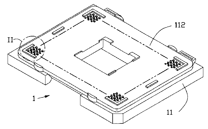
本实用新型电连接器1主要用于电性连接晶片模组(未图示)及电路板(未图示),如图1至图3所示,该电连接器1包括绝缘本体11、收容于绝缘本体11中的若干导电端子12,导电端子12与易熔性焊接元件相配合,在本实施方式中,易熔性焊接元件为锡球13。The utility model
绝缘本体11包括与晶片模组相配合的配合面111、与配合面111相对设置的与电路板相组接的安装面112、贯穿配合面111和安装面112用于收容相应导电端子12的端子孔113以及于安装面112上延伸设置的与绝缘本体11一体成型的保护装置114。该保护装置114呈柱状结构分布于安装面112上相邻两端子孔113之间,其包括本体1141、于本体1141远离安装面112的一端延伸设置的底面1142。The
导电端子12包括主体121、于主体121一端朝向配合面111延伸设置的与晶片模组导电体相配合的接触部122、于主体121另一端延伸设置的与电路板相组接的焊接部123;该焊接部123于其末端延伸设有突出端子孔113外的焊接面1231。沿与电路板相垂直的方向,保护装置114的底面1142到安装面112的垂直距离大于或者等于导电端子12的焊接面1231到安装面112的垂直距离而小于锡球13与焊接面1231配合后其至安装面112的垂直距离。The
使用时,先通过锡球13使导电端子12的焊接部123与电路板导电体相组接使电连接器3组接于电路板,使晶片模组固定于绝缘本体11上使其导电体与导电端子12的接触部122相配合,从而实现电连接器1与晶片模组及电路板之间的电性连接。由于底面1142到安装面112的垂直距离大于或者等于导电端子12的焊接面1231到安装面112的垂直距离,故可以避免水平方向上的外力碰撞导电端子12突伸于端子孔113外的焊接部123导致破坏其平面度而影响电连接器1与电路板的连接效果。During use, the welding portion 123 of the
图4所示为本实用新型另一实施例电连接器1’的立体组合图。电连接器1’包括绝缘本体11’、收容于绝缘本体11’中的若干导电端子12。Fig. 4 is a three-dimensional assembled view of an electrical connector 1' according to another embodiment of the present invention. The electrical connector 1' includes an insulating body 11' and a plurality of
如图5和图6所示,绝缘本体11’包括与晶片模组相配合的配合面111’、与配合面111’相对设置的与电路板相组接的安装面112’、贯穿配合面111’和安装面112’用于收容相应导电端子12的端子孔113’、于其安装面112’延伸设置的与绝缘本体11’一体成型的保护装置114’。该保护装置114’呈长条状结构分布于安装面112’上横向相邻两排端子孔和纵向两排端子孔之间,其包括本体1141’、于本体1141’远离安装面112’的一端设置的底面1142’。如图4所示,底面1142’到安装面112’的垂直距离大于或者等于导电端子12的焊接部123的焊接面1231到安装面112’的垂直距离,故可以避免外力将导电端子12突伸于端子孔113’外的焊接部123导致破坏其平面度而影响电连接器1’与电路板的连接效果。As shown in Figures 5 and 6, the insulating body 11' includes a mating surface 111' matched with the chip module, a mounting surface 112' opposite to the mating surface 111' and assembled with a circuit board, and a penetrating mating surface 111 ' and the mounting surface 112' are used to accommodate the terminal hole 113' of the corresponding
以上为本案两种较佳实施方式,于其它实施方式中,保护装置除了可以与绝缘本体一体成型设置于安装面外,还可以通过其它的配合方式设置于绝缘本体的安装面上。The above are the two preferred implementations of this case. In other implementations, the protection device can be installed on the installation surface of the insulation body in addition to being integrated with the insulation body, and can also be installed on the installation surface of the insulation body through other matching methods.
Claims (8)
Priority Applications (2)
| Application Number | Priority Date | Filing Date | Title |
|---|---|---|---|
| CNU2004200253717U CN2697858Y (en) | 2004-03-12 | 2004-03-12 | Electric connector |
| US11/078,164 US7217996B2 (en) | 2004-03-12 | 2005-03-10 | Ball grid array socket having improved housing |
Applications Claiming Priority (1)
| Application Number | Priority Date | Filing Date | Title |
|---|---|---|---|
| CNU2004200253717U CN2697858Y (en) | 2004-03-12 | 2004-03-12 | Electric connector |
Publications (1)
| Publication Number | Publication Date |
|---|---|
| CN2697858Y true CN2697858Y (en) | 2005-05-04 |
Family
ID=34770945
Family Applications (1)
| Application Number | Title | Priority Date | Filing Date |
|---|---|---|---|
| CNU2004200253717U Expired - Lifetime CN2697858Y (en) | 2004-03-12 | 2004-03-12 | Electric connector |
Country Status (2)
| Country | Link |
|---|---|
| US (1) | US7217996B2 (en) |
| CN (1) | CN2697858Y (en) |
Cited By (1)
| Publication number | Priority date | Publication date | Assignee | Title |
|---|---|---|---|---|
| CN101136515B (en) * | 2006-09-01 | 2010-11-17 | 富士康(昆山)电脑接插件有限公司 | Electrical connector |
Families Citing this family (43)
| Publication number | Priority date | Publication date | Assignee | Title |
|---|---|---|---|---|
| US9536815B2 (en) | 2009-05-28 | 2017-01-03 | Hsio Technologies, Llc | Semiconductor socket with direct selective metalization |
| US8955215B2 (en) | 2009-05-28 | 2015-02-17 | Hsio Technologies, Llc | High performance surface mount electrical interconnect |
| US9276336B2 (en) | 2009-05-28 | 2016-03-01 | Hsio Technologies, Llc | Metalized pad to electrical contact interface |
| WO2010147939A1 (en) | 2009-06-17 | 2010-12-23 | Hsio Technologies, Llc | Semiconductor socket |
| US8955216B2 (en) | 2009-06-02 | 2015-02-17 | Hsio Technologies, Llc | Method of making a compliant printed circuit peripheral lead semiconductor package |
| US8987886B2 (en) | 2009-06-02 | 2015-03-24 | Hsio Technologies, Llc | Copper pillar full metal via electrical circuit structure |
| US9232654B2 (en) | 2009-06-02 | 2016-01-05 | Hsio Technologies, Llc | High performance electrical circuit structure |
| US9613841B2 (en) | 2009-06-02 | 2017-04-04 | Hsio Technologies, Llc | Area array semiconductor device package interconnect structure with optional package-to-package or flexible circuit to package connection |
| US8912812B2 (en) | 2009-06-02 | 2014-12-16 | Hsio Technologies, Llc | Compliant printed circuit wafer probe diagnostic tool |
| WO2011002709A1 (en) | 2009-06-29 | 2011-01-06 | Hsio Technologies, Llc | Compliant printed circuit semiconductor tester interface |
| US8525346B2 (en) | 2009-06-02 | 2013-09-03 | Hsio Technologies, Llc | Compliant conductive nano-particle electrical interconnect |
| US9184527B2 (en) | 2009-06-02 | 2015-11-10 | Hsio Technologies, Llc | Electrical connector insulator housing |
| US9196980B2 (en) | 2009-06-02 | 2015-11-24 | Hsio Technologies, Llc | High performance surface mount electrical interconnect with external biased normal force loading |
| US9603249B2 (en) | 2009-06-02 | 2017-03-21 | Hsio Technologies, Llc | Direct metalization of electrical circuit structures |
| US8988093B2 (en) | 2009-06-02 | 2015-03-24 | Hsio Technologies, Llc | Bumped semiconductor wafer or die level electrical interconnect |
| WO2010141295A1 (en) | 2009-06-02 | 2010-12-09 | Hsio Technologies, Llc | Compliant printed flexible circuit |
| WO2010141311A1 (en) | 2009-06-02 | 2010-12-09 | Hsio Technologies, Llc | Compliant printed circuit area array semiconductor device package |
| US9318862B2 (en) | 2009-06-02 | 2016-04-19 | Hsio Technologies, Llc | Method of making an electronic interconnect |
| US9930775B2 (en) | 2009-06-02 | 2018-03-27 | Hsio Technologies, Llc | Copper pillar full metal via electrical circuit structure |
| WO2011002712A1 (en) | 2009-06-29 | 2011-01-06 | Hsio Technologies, Llc | Singulated semiconductor device separable electrical interconnect |
| US8970031B2 (en) | 2009-06-16 | 2015-03-03 | Hsio Technologies, Llc | Semiconductor die terminal |
| US9277654B2 (en) | 2009-06-02 | 2016-03-01 | Hsio Technologies, Llc | Composite polymer-metal electrical contacts |
| US9699906B2 (en) | 2009-06-02 | 2017-07-04 | Hsio Technologies, Llc | Hybrid printed circuit assembly with low density main core and embedded high density circuit regions |
| WO2010141264A1 (en) | 2009-06-03 | 2010-12-09 | Hsio Technologies, Llc | Compliant wafer level probe assembly |
| WO2010141303A1 (en) | 2009-06-02 | 2010-12-09 | Hsio Technologies, Llc | Resilient conductive electrical interconnect |
| US8610265B2 (en) | 2009-06-02 | 2013-12-17 | Hsio Technologies, Llc | Compliant core peripheral lead semiconductor test socket |
| US9276339B2 (en) | 2009-06-02 | 2016-03-01 | Hsio Technologies, Llc | Electrical interconnect IC device socket |
| WO2012078493A1 (en) | 2010-12-06 | 2012-06-14 | Hsio Technologies, Llc | Electrical interconnect ic device socket |
| WO2010141297A1 (en) | 2009-06-02 | 2010-12-09 | Hsio Technologies, Llc | Compliant printed circuit wafer level semiconductor package |
| WO2012074963A1 (en) * | 2010-12-01 | 2012-06-07 | Hsio Technologies, Llc | High performance surface mount electrical interconnect |
| WO2010141318A1 (en) | 2009-06-02 | 2010-12-09 | Hsio Technologies, Llc | Compliant printed circuit peripheral lead semiconductor test socket |
| WO2010141313A1 (en) | 2009-06-02 | 2010-12-09 | Hsio Technologies, Llc | Compliant printed circuit socket diagnostic tool |
| WO2010141296A1 (en) | 2009-06-02 | 2010-12-09 | Hsio Technologies, Llc | Compliant printed circuit semiconductor package |
| US9184145B2 (en) | 2009-06-02 | 2015-11-10 | Hsio Technologies, Llc | Semiconductor device package adapter |
| US8981568B2 (en) | 2009-06-16 | 2015-03-17 | Hsio Technologies, Llc | Simulated wirebond semiconductor package |
| US8758067B2 (en) | 2010-06-03 | 2014-06-24 | Hsio Technologies, Llc | Selective metalization of electrical connector or socket housing |
| US9689897B2 (en) | 2010-06-03 | 2017-06-27 | Hsio Technologies, Llc | Performance enhanced semiconductor socket |
| US9350093B2 (en) | 2010-06-03 | 2016-05-24 | Hsio Technologies, Llc | Selective metalization of electrical connector or socket housing |
| US10159154B2 (en) | 2010-06-03 | 2018-12-18 | Hsio Technologies, Llc | Fusion bonded liquid crystal polymer circuit structure |
| US9761520B2 (en) | 2012-07-10 | 2017-09-12 | Hsio Technologies, Llc | Method of making an electrical connector having electrodeposited terminals |
| US10506722B2 (en) | 2013-07-11 | 2019-12-10 | Hsio Technologies, Llc | Fusion bonded liquid crystal polymer electrical circuit structure |
| US10667410B2 (en) | 2013-07-11 | 2020-05-26 | Hsio Technologies, Llc | Method of making a fusion bonded circuit structure |
| US9559447B2 (en) | 2015-03-18 | 2017-01-31 | Hsio Technologies, Llc | Mechanical contact retention within an electrical connector |
Family Cites Families (4)
| Publication number | Priority date | Publication date | Assignee | Title |
|---|---|---|---|---|
| TW399789U (en) * | 1999-02-02 | 2000-07-21 | Hon Hai Prec Ind Co Ltd | Electrical connector |
| JP2001007473A (en) * | 1999-06-17 | 2001-01-12 | Nec Corp | Integrated circuit device mounting structure and method |
| US6438826B2 (en) * | 2000-02-10 | 2002-08-27 | Towa Corporation | Electronic component, method of sealing electronic component with resin, and apparatus therefor |
| US6558170B1 (en) * | 2000-11-22 | 2003-05-06 | Fci Americas Technology, Inc. | Strain relief for BGA connector |
-
2004
- 2004-03-12 CN CNU2004200253717U patent/CN2697858Y/en not_active Expired - Lifetime
-
2005
- 2005-03-10 US US11/078,164 patent/US7217996B2/en not_active Expired - Fee Related
Cited By (1)
| Publication number | Priority date | Publication date | Assignee | Title |
|---|---|---|---|---|
| CN101136515B (en) * | 2006-09-01 | 2010-11-17 | 富士康(昆山)电脑接插件有限公司 | Electrical connector |
Also Published As
| Publication number | Publication date |
|---|---|
| US7217996B2 (en) | 2007-05-15 |
| US20050200016A1 (en) | 2005-09-15 |
Similar Documents
| Publication | Publication Date | Title |
|---|---|---|
| CN2697858Y (en) | Electric connector | |
| US10741951B2 (en) | Socket connector assembly for an electronic package | |
| CN2713666Y (en) | Electric connector assembly | |
| CN2417578Y (en) | Electric connector | |
| CN2638272Y (en) | Electric connector | |
| CN2513241Y (en) | Large flow socket connector | |
| CN2731753Y (en) | Socket connector | |
| CN2840355Y (en) | Flexible circuit board and electric connector with the same flexible circuit board | |
| CN2766391Y (en) | Electric connector | |
| CN101212097A (en) | electrical connector terminal | |
| CN200972994Y (en) | Electric connector terminal | |
| JP3772304B2 (en) | Interconnection structure of printed circuit boards | |
| CN201142393Y (en) | electrical connector | |
| CN201178149Y (en) | electrical connector | |
| CN1242513C (en) | Low-profile connector | |
| CN102315543B (en) | Electric connector | |
| CN101154782B (en) | Electric connector and manufacturing method thereof | |
| CN102270784B (en) | Electric connector | |
| CN103208707B (en) | Electric connector | |
| CN2770129Y (en) | Electric connector terminal | |
| US8070496B2 (en) | Contact terminal unit and socket connector incorporated with the same contact terminal units | |
| TWI424617B (en) | Electrical connector | |
| CN107465006B (en) | Busbar, coupling assembling, connector and central electrical apparatus box | |
| CN220209351U (en) | Wire connector | |
| TW201023438A (en) | Electrical connector |
Legal Events
| Date | Code | Title | Description |
|---|---|---|---|
| C14 | Grant of patent or utility model | ||
| GR01 | Patent grant | ||
| C17 | Cessation of patent right | ||
| CX01 | Expiry of patent term |
Expiration termination date: 20140312 Granted publication date: 20050504 |