CN2612071Y - Package structure for chip - Google Patents
Package structure for chip Download PDFInfo
- Publication number
- CN2612071Y CN2612071Y CNU032034334U CN03203433U CN2612071Y CN 2612071 Y CN2612071 Y CN 2612071Y CN U032034334 U CNU032034334 U CN U032034334U CN 03203433 U CN03203433 U CN 03203433U CN 2612071 Y CN2612071 Y CN 2612071Y
- Authority
- CN
- China
- Prior art keywords
- chip
- multilayer interconnection
- interconnection structure
- support base
- internal circuit
- Prior art date
- Legal status (The legal status is an assumption and is not a legal conclusion. Google has not performed a legal analysis and makes no representation as to the accuracy of the status listed.)
- Expired - Lifetime
Links
Images


Classifications
-
- H10W74/15—
-
- H10W90/724—
-
- H10W90/734—
Landscapes
- Wire Bonding (AREA)
Abstract
一种芯片封装结构,至少包括:一多层内连线结构,具有一顶面及对应的一底面,且该多层内连线结构还具有一内部线路,且该内部线路还具有多个接合垫,其位于该多层内连线结构的底面;至少一芯片,配置于该多层内连线结构的该顶面,并电连接于该多层内连线结构的该内部线路;以及一支撑底板,其材质为绝缘材质,且该支撑底板配置于该多层内连线结构之该底面,且该支撑底板更具有多个第一开口,其分别暴露出其所对应的该些接合垫之一。
A chip packaging structure, at least comprising: a multilayer interconnection structure, with a top surface and a corresponding bottom surface, and the multilayer interconnection structure also has an internal circuit, and the internal circuit also has a plurality of joints a pad located on the bottom surface of the multilayer interconnect structure; at least one chip configured on the top surface of the multilayer interconnect structure and electrically connected to the internal circuit of the multilayer interconnect structure; and a The support base plate is made of insulating material, and the support base plate is disposed on the bottom surface of the multilayer interconnection structure, and the support base plate further has a plurality of first openings, which respectively expose the corresponding bonding pads one.
Description
技术领域technical field
本实用新型涉及一种的芯片封装结构,且特别是涉及一种运用由绝缘材质所制成的硬质支撑基板(support base plate)是芯片封装结构。The utility model relates to a chip packaging structure, and in particular to a chip packaging structure using a hard support base plate made of insulating material.
背景技术Background technique
覆晶接合技术(Flip Chip Interconnect Technology,简称FC)乃是利用面数组(area array)的方式,将多个芯片垫(die pad)配置于芯片(die)之有源表面(active sutface)上,并在芯片垫上形成凸块(bump),接着将芯片翻覆(flip)之后,再利用这些凸块来分别电性及机械性连接芯片之芯片垫至承载器(carrier)上的接点(contact),使得芯片可经由凸块而电连接至承载器,并经由承载器之内部线路而电连接至外界之电子装置。值得注意的是,由于覆晶接合技术(FC)系可适用于高脚数(High Pin Count)之芯片封装结构,并同时具有缩小芯片封装面积及缩短讯号传输路径等诸多优点,所以覆晶接合技术目前已经广泛地应用于芯片封装领域,常见应用覆晶接合技术之芯片封装结构例如有覆晶球格数组型(Flip Chip Ball GridArray,FC/BGA)及覆晶针格数组型(Flip Chip Pin Grid Atray,FC/PGA)等型态之芯片封装结构。Flip Chip Interconnect Technology (FC for short) uses an area array to arrange multiple die pads on the active surface of the die. And form bumps (bumps) on the chip pad, and then flip the chip (flip), and then use these bumps to electrically and mechanically connect the chip pad of the chip to the contact on the carrier (carrier), The chip can be electrically connected to the carrier through the bump, and electrically connected to the external electronic device through the internal circuit of the carrier. It is worth noting that because the flip-chip bonding technology (FC) is applicable to high-pin-count (High Pin Count) chip packaging structures, and has many advantages such as reducing the chip packaging area and shortening the signal transmission path, the flip-chip bonding Technology has been widely used in the field of chip packaging. Commonly used chip packaging structures of flip chip bonding technology include flip chip ball grid array (Flip Chip Ball Grid Array, FC/BGA) and flip chip pin grid array (Flip Chip Pin Grid Atray, FC/PGA) and other types of chip packaging structures.
请参考图1,其绘示现有的一种覆晶球格数组型之芯片封装结构的剖面示意图。芯片封装结构100包括基板(substrate)110、多个凸块120、芯片130、及多个焊球140。其中,基板110具有一顶面112及对应之一底面114,且基板110更具有多个凸块垫(bump pad)116a及多个焊球垫(ball pad)116b。此外,芯片130具有一有源表面(active surface)132及对应之一背面134,其中芯片130之有源表面112系泛指芯片130之具有有源组件(active device)(未绘示)的一面,并且芯片130更具有多个芯片垫136,其配置于芯片130之有源表面132,用以作为芯片130之讯号输出入的媒介,其中这些凸块垫116a之位置系分别对应于这些芯片垫136之位置。另外,这些凸块120则分别电性及机械性连接这些芯片垫136之一至其所对应之这些凸块垫116a之一。并且,这些焊球140则分别配置于这些焊球垫116b上,用以电性及机械性连接至外界之电子装置。Please refer to FIG. 1 , which shows a schematic cross-sectional view of a conventional flip-chip ball array chip packaging structure. The
请同样参考第1图,现有之芯片封装制造工艺系完成基板110之内部线路118以及接点116a、116b之后,再将芯片130组装于基板110之表面上,接着将一底胶(underfill)150填充于基板110之顶面112及芯片130之有源表面132所围成的空间,用以保护凸块垫116a、芯片垫136及凸块120所裸露出之部分,并同时缓冲基板110与芯片130之间在受热时所产生的热应变(thermal strain)之不匹配的现象。因此,芯片130之芯片垫136将可经由凸块120而电性及机械性连接至基板110之凸块垫116a,再经由基板110之内部线路118而向下绕线(routing)至基板110之底面114的焊球垫116b,最后经由焊球垫116b上之焊球140而电性及机械性连接至外界之电子装置。Please also refer to FIG. 1, the existing chip packaging manufacturing process is to complete the internal circuit 118 and the
在提高芯片之运算速度及降低芯片之制造成本的考量之下,芯片之面积及芯片垫之间的间隙两者必然逐渐地缩小,意即芯片垫之密度将相对逐渐地升高。因此,当具有高密度芯片垫之芯片采用覆晶(FC)型态,并同时搭配球格数组(BGA)或针格数组(PGA)等型态来进行封装时,由于芯片之相邻的芯片垫的间距都非常微小,此时必须采用具有高密度凸块垫及微细线路之基板,才能将芯片以覆晶接合的方式配置于基板之顶面,并经由基板之内部线路的重新绕线,而将芯片之芯片垫延伸分布到基板之底面,再经由位于基板之底面的焊球(ball)或针脚(pin)等接点,使得芯片最后能够电连接至外界之电子装置。In consideration of improving the operation speed of the chip and reducing the manufacturing cost of the chip, both the area of the chip and the gap between the chip pads must be gradually reduced, which means that the density of the chip pad will be relatively gradually increased. Therefore, when a chip with a high-density chip pad adopts a flip-chip (FC) type and is packaged with a ball grid array (BGA) or pin grid array (PGA) at the same time, due to the adjacent chips of the chip The pitch of the pads is very small. At this time, a substrate with high-density bump pads and fine circuits must be used, so that the chip can be arranged on the top surface of the substrate in a flip-chip bonding manner, and the internal circuit of the substrate can be rewound. The chip pads of the chip are extended and distributed to the bottom surface of the substrate, and then through contacts such as balls or pins located on the bottom surface of the substrate, the chip can finally be electrically connected to external electronic devices.
如上所述,目前覆晶球格数组型(FC/BGA)或覆晶针格数组型(FC/PGA)之基板的常见材质包括有陶瓷(ceramic)及有机材料(organicmaterial)等,目前又以有机材料作为介电层(dielectric layer)之材质的有机基板(organic substrate)较为常见。值得注意的是,由于有机基板受到介电层之热膨胀(thermal expansion)的严重影响,使得现今可大规模量产之有机基板的导线其线宽及线距仅能分别达到25微米及25微米,同时现今可大规模量产之未裁切前有机基板的面板尺寸也仅可到达610×610平方公厘。然而,随着芯片之芯片垫的密度逐渐地升高,在大规模量产的考量之下,如何以低成本之基板封装此种具有高密度芯片垫之芯片,此乃是目前芯片封装产业亟待解决的重大课题之一。As mentioned above, the current common materials of flip-chip ball grid array (FC/BGA) or flip-chip pin grid array (FC/PGA) substrates include ceramics and organic materials. An organic substrate (organic substrate) in which an organic material is used as a material of a dielectric layer is relatively common. It is worth noting that since the organic substrate is severely affected by the thermal expansion of the dielectric layer, the line width and line spacing of the organic substrate that can be mass-produced today can only reach 25 microns and 25 microns, respectively. At the same time, the panel size of the uncut organic substrate that can be mass-produced today can only reach 610×610 square millimeters. However, as the density of die pads of chips increases gradually, under the consideration of large-scale mass production, how to package such chips with high-density die pads with low-cost substrates is an urgent need for the current chip packaging industry. One of the major issues to be solved.
实用新型内容Utility model content
有鉴于此,本实用新型的任务就是在提供一种芯片封装结构,可以提供高密度焊垫(凸块垫)及微细线路的多层内连线结构,并可有效降低芯片封装结构的制作成本。In view of this, the task of the present utility model is to provide a chip packaging structure, which can provide a multilayer interconnection structure of high-density solder pads (bump pads) and fine lines, and can effectively reduce the manufacturing cost of the chip packaging structure. .
为了完成上述任务,本实用新型提供一种芯片封装结构,至少包括:一多层内连线结构,具有一顶面及对应的一底面,且该多层内连线结构还具有一内部线路,且该内部线路还具有多个接合垫,其位于该多层内连线结构的底面;至少一芯片,配置于该多层内连线结构的该顶面,并电连接于该多层内连线结构的该内部线路;以及一支撑底板,其材质为绝缘材质,且该支撑底板配置于该多层内连线结构之该底面,且该支撑底板更具有多个第一开口,其分别暴露出其所对应的该些接合垫之一。In order to accomplish the above tasks, the utility model provides a chip packaging structure, which at least includes: a multilayer interconnection structure with a top surface and a corresponding bottom surface, and the multilayer interconnection structure also has an internal circuit, And the internal circuit also has a plurality of bonding pads, which are located on the bottom surface of the multilayer interconnection structure; at least one chip is arranged on the top surface of the multilayer interconnection structure, and is electrically connected to the multilayer interconnection structure. The internal circuit of the wire structure; and a supporting base plate, the material of which is insulating material, and the supporting base plate is arranged on the bottom surface of the multi-layer interconnection structure, and the supporting base plate further has a plurality of first openings, which respectively expose one of the bond pads to which it corresponds.
为达本实用新型的上述目的,本实用新型提出一种芯片封装结构,此芯片封装结构主要包括一多层内连线结构(multi-layer interconnectionstructure)、至少一芯片、一隔绝底层(isolation base layer)以及一支撑底板(support base plate)。其中,多层内连线结构具有一顶面及对应之一底面,且多层内连线结构更具有一内部线路(inner circuit),且内部线路更具有多个接合垫,其位于多层内连线结构之底面。此外,芯片配置于多层内连线结构之顶面,并电连接于多层内连线结构之内部线路。另外,隔绝底层及支撑底板系配置于多层内连线结构之底面,而隔绝底层更具有多个第二开口,且支撑底板更具有多个第一开口,其分别连通于其所对应的这些第二开口之一,且分别暴露出其所对应之这些接合垫之一。In order to achieve the above purpose of the utility model, the utility model proposes a chip packaging structure, which mainly includes a multi-layer interconnection structure (multi-layer interconnection structure), at least one chip, and an isolation base layer ) and a support base plate. Wherein, the multilayer interconnection structure has a top surface and a corresponding bottom surface, and the multilayer interconnection structure further has an inner circuit (inner circuit), and the inner circuit further has a plurality of bonding pads, which are located in the multilayer The bottom surface of the wiring structure. In addition, the chip is arranged on the top surface of the multilayer interconnection structure, and is electrically connected to the internal circuit of the multilayer interconnection structure. In addition, the isolation bottom layer and the support base plate are arranged on the bottom surface of the multilayer interconnection structure, and the isolation base layer further has a plurality of second openings, and the support base plate further has a plurality of first openings, which are respectively connected to the corresponding ones. One of the second openings respectively exposes one of the corresponding bonding pads.
为达本实用新型的上述目的,本实用新型提出一种芯片封装制造工艺,包括(a)提供一支撑底板,支撑底板具有一顶面及对应之一底面;(b)形成一多层内连线结构于支撑底板之上,且多层内连线结构具有一内部线路,且内部线路更具有多个接合垫,其位于多层内连线结构之接近支撑底板之一面;(c)配置至少一芯片于多层内连线结构之远离支撑底板之一面,且芯片系电连接于多层内连线结构之内部线路;(d)形成多个第一开口于支撑底板上,而这些第一开口系分别暴露出其所对应之这些接合垫之一。In order to achieve the above purpose of the utility model, the utility model proposes a chip packaging manufacturing process, including (a) providing a support base plate, the support base plate has a top surface and a corresponding bottom surface; (b) forming a multi-layer interconnection The line structure is on the support base plate, and the multilayer interconnection structure has an internal circuit, and the internal circuit further has a plurality of bonding pads, which are located on a side of the multilayer interconnection structure close to the support base plate; (c) disposing at least A chip is on the side of the multilayer interconnect structure away from the support base, and the chip is electrically connected to the internal circuit of the multilayer interconnect structure; (d) forming a plurality of first openings on the support base, and these first The openings respectively expose one of the corresponding bonding pads.
依照本实用新型的优选实施例所述,上述的支撑底板的材质为玻璃(glass)、石英(quartz)或陶瓷(ceramic)等硬质绝缘材料,而形成第一开口于支撑底板上的方法,包括超音波穿孔、激光烧孔或蚀刻等。此外,在芯片封装结构中,芯片系以覆晶接合、打线接合或热压接合的方式,电连接至多层内连线结构之内部线路。再者,更可形成多个接点于支撑底板之远离芯片的一面,而这些接点系分别连接至其所对应之这些接合垫之一,其中这些接点例如为焊球、针脚或电极凸块。According to the preferred embodiment of the present utility model, the material of the above-mentioned support base plate is a hard insulating material such as glass (glass), quartz (quartz) or ceramic (ceramic), and the method of forming the first opening on the support base plate, Including ultrasonic perforation, laser burning or etching, etc. In addition, in the chip packaging structure, the chip is electrically connected to the internal circuit of the multilayer interconnection structure by means of flip chip bonding, wire bonding or thermocompression bonding. Moreover, a plurality of contacts can be formed on the side of the support base far away from the chip, and these contacts are respectively connected to one of the corresponding bonding pads, wherein the contacts are solder balls, pins or electrode bumps, for example.
因此,本实用新型是利用薄膜晶体管液晶显示面板(TFT-LCD panel)或集成电路(IC)之制造工艺技术及生产机台,在以玻璃、石英或陶瓷为材质之大面积及高平坦度的支撑底板上,形成一具有高密度焊垫(凸块垫)及微细线路之多层内连线结构,接着再以覆晶接合的方式将芯片配置于多层内连线结构之顶面,并在支撑底板之底面形成多个开口,最后将接点配置于支撑底板之开口中,并电连接于多层内连线结构之接合垫,而完成本实用新型的芯片封装制造工艺。Therefore, the utility model utilizes the manufacturing technology and production machine of thin film transistor liquid crystal display panel (TFT-LCD panel) or integrated circuit (IC), in the large-area and high flatness that take glass, quartz or pottery as material Form a multilayer interconnection structure with high-density solder pads (bump pads) and fine lines on the support base plate, and then place the chip on the top surface of the multilayer interconnection structure by flip-chip bonding, and A plurality of openings are formed on the bottom surface of the supporting base, and finally the contacts are arranged in the openings of the supporting base and electrically connected to the bonding pads of the multilayer interconnection structure, thereby completing the chip packaging manufacturing process of the present invention.
为让本实用新型的上述和其它目的、特征、和优点能更明显易懂,下文特举一优选实施例,并配合所附图式,作详细说明如下:In order to make the above and other purposes, features, and advantages of the present utility model more obvious and understandable, a preferred embodiment is specifically cited below, and is described in detail as follows in conjunction with the accompanying drawings:
附图说明Description of drawings
图1绘示现有的一种覆晶球格数组型的芯片封装结构的剖面示意图;以及FIG. 1 shows a schematic cross-sectional view of a conventional flip-chip ball array chip packaging structure; and
图2A~2G依序绘示本实用新型的优选实施例的一种芯片封装制造工艺的流程示意图。2A-2G sequentially illustrate a schematic flow chart of a chip packaging manufacturing process according to a preferred embodiment of the present invention.
附图标号说明Explanation of reference numbers
100:芯片封装结构 110:基板100: Chip package structure 110: Substrate
112:顶面 114:底面112: top surface 114: bottom surface
116a:凸块垫 116b:焊球垫116a:
120:凸块 130:芯片120: Bump 130: Chip
132:有源表面 134:背面132: active surface 134: back
136:芯片垫 140:焊球136: chip pad 140: solder ball
150:底胶150: primer
200:芯片封装结构 202:支撑底板200: Chip package structure 202: Support base plate
202a:第一开口 204:隔绝底层202a: First opening 204: Isolate the bottom layer
204a:第二开 206:多层内连线结构204a: Second opening 206: Multi-layer interconnection structure
206a:顶面 206b:底面206a: top surface 206b: bottom surface
208:导线层 208a:凸块垫208: wire layer 208a: bump pad
208b:接合垫 210:介电层208b: bonding pad 210: dielectric layer
212:导电插塞 214:内部线路212: Conductive plug 214: Internal wiring
216:芯片 216a:有源表面216: chip 216a: active surface
216b:背面 218:芯片垫216b: Back side 218: Chip pad
220:凸块 230:接点220: Bump 230: Contact
具体实施方式Detailed ways
图2A~2G依序绘示本实用新型的优选实施例的一种芯片封装制造工艺的流程示意图。首先如图2A所示,提供一支撑底板202,其材质为绝缘材质,例如为玻璃、石英或陶瓷等,并且支撑底板202的表面必须具有较高等级的平坦度(co-planarity)。接着如图2B所示,形成一隔绝底层204于支撑底板202之上,并可选择性地平坦化隔绝底层204之表面,使得隔绝底层204之表面亦具有较高等级的平坦度,其中隔绝底层204之材质例如为聚合物(polymer)、聚酯(polyestet)、聚酰乙胺(PolyImide,PI)、环氧树脂(epoxy resin)、压克力及苯(并)环丁烯(BenzoCycloButene,BCB)等,并可利用薄膜贴附(film attachment)或薄层涂布(coating)的方式,将隔绝底层204形成于支撑底板202之上。2A-2G sequentially illustrate a schematic flow chart of a chip packaging manufacturing process according to a preferred embodiment of the present invention. First, as shown in FIG. 2A , a
接着如图2C所示,形成一多层内连线结构206于隔绝底层204之上。其中,多层内连线结构206主要包括图案化之多个导线层208、至少一介电层210及多个导电插塞212,且这些导线层208系依序重迭于隔绝底层204之上,而介电层210则配置于两相邻之导线层208之间,且这些导电插塞212系分别贯穿介电层210而电连接两相邻之导线层208,并且这些导线层208及这些导电插塞212系构成一内部线路214。其中,内部线路214系在多层内连线结构206的底面206b形成多个接合垫208b。此外,导线层208之材质例如为铜、铝及该等合金,通常为铝或铜,而介电层210之材质例如为氮化硅(silicon nitride)、氧化硅(silicon oxide)或环氧树脂(epoxy resin)等聚合物等。值得注意的是,隔绝底层204系可选择性地配置于支撑底板202之上,因此,当多层内连线结构206将可直接形成于支撑底板202之上时,则无须配置隔绝底层204于支撑底板202之上,然而这样的情况并未绘示于图2B~2G。Next, as shown in FIG. 2C , a
同样如图2C所示,由于本实用新型乃是利用液晶显示面板或集成电路等相关之制造工艺技术,来形成此一多层内连线结构206于隔绝底层204之上,使得多层内连线结构206的内部线路214的线宽及线距其范围均可在1~50微米的范围之间,且特别是在1~数微米的范围之间。因此,与现有之第1图所示之以有机材料为介电层材质的基板110相较之下,此处所制作出之多层内连线结构206将可提供更高密度焊垫(凸块垫)及更微细的线路。此外,在形成多层内连线结构206于隔绝底层204之上时,更可配设无源组件(passive component)(未绘示)于多层内连线结构206之内部或顶面206a,并电连接于多层内连线结构206之内部线路214,或者是利用内部线路214之特殊的绕线设计来形成电容及电感等无源组件。Also as shown in FIG. 2C, since the utility model utilizes related manufacturing techniques such as liquid crystal display panels or integrated circuits, to form this
接着如图2D所示,在完成多层内连线结构206之制造工艺之后,还可以一研磨机来薄化支撑底板202之厚度,接着如图2E所示,以覆晶接合的方式,配置至少一芯片216于多层内连线结构206之远离支撑底板202之一面,且芯片216系电连接于多层内连线结构206之内部线路214。当然,上述之薄化支撑底板202的步骤,亦可在配置芯片216于多层内连线结构206之后始进行。此外,芯片216具有一有源表面216a及一背面216b,且芯片216更具有多个芯片垫218,其位于芯片216之有源表面216a。另外,更将多个凸块220分别电性及机械性连接这些芯片垫218之一至其所对应之这些凸块垫208a之一,故可以覆晶接合的方式,将芯片216配置于多层内连线结构206之上,并将芯片216电连接于多层内连线结构206之内部线路214。当然,芯片216亦可以打线接合(wire bonding)或热压接合(thermalcompression bonding)的方式,而电连接于多层内连线结构206之内部线路214。Next, as shown in FIG. 2D, after completing the manufacturing process of the
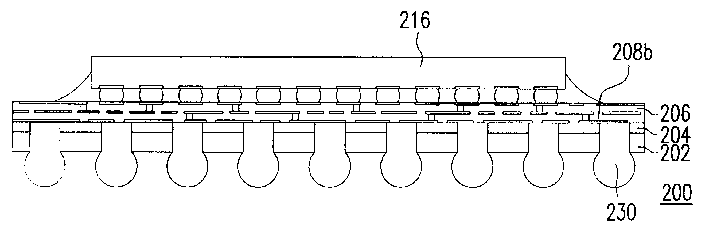
接着如图2F所示,以超音波穿孔、激光烧孔或蚀刻等方式来形成多个第一开口(opening)202a于支撑底板202上,且在形成多个第一开口202a之后,更可以同样的方式形成第二开口204a于绝缘底层204上。其中,第二开口204a分别连通其所对应之第一开口202a之一,并分别暴露出其所对应之这些接合垫208b之一。最后如图2G所示,形成多个接点230于支撑底板202之远离芯片216之一面,且这些接点230系分别连接至其所对应之这些接合垫208b之一,其中接脚可为焊球、针脚或电极凸块等导电结构,并且以面数组的方式配置于芯片封装结构200之底面。Next, as shown in FIG. 2F , a plurality of first openings (opening) 202a are formed on the
此外,如图2G所示,可在配置接点230于接合垫208b之后,再进行切单作业,用以分割出单颗芯片封装结构200。接着如图2F所示,亦可在配置接点230于接合垫208b之前,即进行切单作业,用以分割出单颗芯片封装结构200。值得注意的是,由于本实用新型的芯片封装结构200系可适用于封装多个芯片216,并可经由多层内连线结构206之内部线路214而相互电连接,故此芯片封装结构200将可应用于多重芯片模块(Multiple ChipModule,MCM)及系统于单一封装(System In Package,SIP)。再者,芯片216之背面216b还可选择性地配置一散热片(heat sink)(未绘示),其材质为散热性佳之材料,例如铜、铝及该等之合金,用以增加芯片封装结构200之散热效能。In addition, as shown in FIG. 2G , after the contacts 230 are arranged on the
综上所述,本实用新型系可将液晶显示面板或集成电路之制造工艺技术及生产机台,加以整合应用到本实用新型的芯片封装制造工艺。值得注意的是,由于液晶显示面板及集成电路之制造工艺技术目前已经非常地成熟,所以在大规模量产的情况之下,本实用新型的芯片封装制造工艺将可在平面尺寸大于610×610平方公厘以上之支撑底板上,同时形成一具有高密度焊垫(凸块垫)及微细线路的多层内连线结构,接着再以覆晶接合,甚至是打线接合或热压接合的方式,将芯片配置于此内连线层多层内连线结构之上,如此将可使本实用新型采用玻璃基板之芯片封装的成本低于现有采用有机基板之芯片封装的成本。To sum up, the present invention can integrate the manufacturing technology and production machine of liquid crystal display panels or integrated circuits into the chip packaging manufacturing process of the present invention. It is worth noting that since the manufacturing technology of liquid crystal display panels and integrated circuits is very mature, under the condition of large-scale mass production, the chip packaging manufacturing technology of the present invention will be able to make the plane size larger than 610×610 On the support base plate with a square millimeter or more, a multi-layer interconnection structure with high-density solder pads (bump pads) and fine lines is formed at the same time, and then flip-chip bonding, or even wire bonding or thermocompression bonding In this way, the chip is arranged on the multilayer interconnection structure of the interconnection layer, so that the cost of the chip package using the glass substrate of the present invention is lower than that of the existing chip package using the organic substrate.
此外,由于液晶显示面板之制造工艺技术所能制作出之导线的线宽及线距均可达到1微米,甚至小于1微米,所以在芯片之芯片垫的密度逐渐升高的情况之下,本实用新型的芯片封装制造工艺将可完全配合芯片之芯片垫的密度,而对应提供高密度焊垫(凸块垫)及微细线路之多层内连线结构,同时更易于控制多层内连线结构之导线的单位电性阻抗,而这些特点均是现有采用有机基板之芯片封装制造工艺所无法轻易达成的。In addition, because the line width and line spacing of the wires that can be produced by the manufacturing technology of the liquid crystal display panel can reach 1 micron, or even less than 1 micron, so under the situation that the density of the chip pad is gradually increasing, this The utility model chip packaging manufacturing process will fully match the density of the chip pad, and provide high-density solder pads (bump pads) and a multi-layer interconnection structure with fine lines, and it is easier to control the multi-layer interconnection The unit electrical impedance of the wires of the structure, and these characteristics cannot be easily achieved by the existing chip packaging manufacturing process using organic substrates.
另外,同样由于液晶显示面板之制造工艺技术所能制作出之导线的线宽及线距均可达到1微米,甚至小于1微米,所以本实用新型的芯片封装制造工艺将可完全配合芯片之芯片垫的密度,而对应提供高密度焊垫(凸块垫)及微细线路之多层内连线结构,所以芯片之芯片垫的密度将可逐渐地提高,因而相对缩小单颗芯片之面积,使得同一片晶圆所能切割出之芯片的总数将可相对提高,故如此将有助于降低单颗芯片之制作成本,因而连带降低芯片封装结构之整体的制作成本。In addition, also because the line width and line spacing of the wires that can be produced by the manufacturing technology of the liquid crystal display panel can reach 1 micron, or even less than 1 micron, so the chip packaging manufacturing process of the present utility model can fully match the chip of the chip. The density of the pad corresponds to the multi-layer interconnection structure that provides high-density solder pads (bump pads) and fine lines, so the density of the chip pad of the chip will gradually increase, thus relatively reducing the area of a single chip, making The total number of chips that can be cut out of the same wafer will be relatively increased, so this will help to reduce the production cost of a single chip, thereby reducing the overall production cost of the chip package structure.
虽然本实用新型已结合一优选实施例揭露如上,然而其并非用以限定本实用新型,本领域的技术人员在不脱离本实用新型的精神和范围内,可作出些许的更动与润饰,因此本实用新型的保护范围应当视后附的权利要求的范围所界定者为准。Although the utility model has been disclosed above in conjunction with a preferred embodiment, it is not intended to limit the utility model, and those skilled in the art can make some changes and modifications without departing from the spirit and scope of the utility model, so The protection scope of the present utility model should be defined by the appended claims.
Claims (10)
Priority Applications (1)
| Application Number | Priority Date | Filing Date | Title |
|---|---|---|---|
| CNU032034334U CN2612071Y (en) | 2003-02-27 | 2003-02-27 | Package structure for chip |
Applications Claiming Priority (1)
| Application Number | Priority Date | Filing Date | Title |
|---|---|---|---|
| CNU032034334U CN2612071Y (en) | 2003-02-27 | 2003-02-27 | Package structure for chip |
Publications (1)
| Publication Number | Publication Date |
|---|---|
| CN2612071Y true CN2612071Y (en) | 2004-04-14 |
Family
ID=34158130
Family Applications (1)
| Application Number | Title | Priority Date | Filing Date |
|---|---|---|---|
| CNU032034334U Expired - Lifetime CN2612071Y (en) | 2003-02-27 | 2003-02-27 | Package structure for chip |
Country Status (1)
| Country | Link |
|---|---|
| CN (1) | CN2612071Y (en) |
Cited By (4)
| Publication number | Priority date | Publication date | Assignee | Title |
|---|---|---|---|---|
| US7944051B2 (en) | 2007-07-23 | 2011-05-17 | Renesas Electronics Corporation | Semiconductor device having external connection terminals and method of manufacturing the same |
| CN102867759A (en) * | 2012-08-17 | 2013-01-09 | 日月光半导体制造股份有限公司 | Semiconductor package structure and manufacturing method thereof |
| CN103474364A (en) * | 2013-09-04 | 2013-12-25 | 惠州硕贝德无线科技股份有限公司 | Novel semiconductor packaging method |
| CN106257658A (en) * | 2015-06-22 | 2016-12-28 | 华亚科技股份有限公司 | Semiconductor device with a plurality of transistors |
-
2003
- 2003-02-27 CN CNU032034334U patent/CN2612071Y/en not_active Expired - Lifetime
Cited By (6)
| Publication number | Priority date | Publication date | Assignee | Title |
|---|---|---|---|---|
| US7944051B2 (en) | 2007-07-23 | 2011-05-17 | Renesas Electronics Corporation | Semiconductor device having external connection terminals and method of manufacturing the same |
| CN102867759A (en) * | 2012-08-17 | 2013-01-09 | 日月光半导体制造股份有限公司 | Semiconductor package structure and manufacturing method thereof |
| CN102867759B (en) * | 2012-08-17 | 2015-04-29 | 日月光半导体制造股份有限公司 | Semiconductor package structure and manufacturing method thereof |
| CN103474364A (en) * | 2013-09-04 | 2013-12-25 | 惠州硕贝德无线科技股份有限公司 | Novel semiconductor packaging method |
| CN103474364B (en) * | 2013-09-04 | 2016-11-09 | 惠州硕贝德无线科技股份有限公司 | A kind of novel method for packaging semiconductor |
| CN106257658A (en) * | 2015-06-22 | 2016-12-28 | 华亚科技股份有限公司 | Semiconductor device with a plurality of transistors |
Similar Documents
| Publication | Publication Date | Title |
|---|---|---|
| US6951773B2 (en) | Chip packaging structure and manufacturing process thereof | |
| US6294407B1 (en) | Microelectronic packages including thin film decal and dielectric adhesive layer having conductive vias therein, and methods of fabricating the same | |
| CN102543927B (en) | Encapsulation substrate embedded with through-hole interposer and manufacturing method thereof | |
| TWI476888B (en) | Package substrate with embedded perforation interposer and preparation method thereof | |
| TWI303096B (en) | ||
| US20040046254A1 (en) | Integrated chip package structure using metal substrate and method of manufacturing the same | |
| CN1388584A (en) | Semiconductor device | |
| JP3651346B2 (en) | Semiconductor device and manufacturing method thereof | |
| CN104051354A (en) | Semiconductor package and fabrication method thereof | |
| TWI581387B (en) | Package structure and its manufacturing method | |
| TW201417235A (en) | Package structure and its manufacturing method | |
| US7038309B2 (en) | Chip package structure with glass substrate | |
| TWI622153B (en) | System-in-package and method for fabricating the same | |
| CN2613046Y (en) | Chip packaging structure | |
| US20240222213A1 (en) | Embedded silicon-based device components in a thick core substrate of an integrated circuit package | |
| KR20230134440A (en) | Structure of package substrate | |
| TWI233190B (en) | Structure of chip package and process thereof | |
| CN115312490B (en) | Electronic module, manufacturing method thereof and electronic package | |
| CN2612071Y (en) | Package structure for chip | |
| CN2591772Y (en) | Chip package structure | |
| TW202322327A (en) | Chip packaging structure and manufacturing method thereof | |
| CN101266955A (en) | Semiconductor device and method for manufacturing the same | |
| CN2598137Y (en) | Chip package structure | |
| CN118398590B (en) | Electronic package and package substrate and manufacturing method thereof | |
| CN2672856Y (en) | Chip package structure |
Legal Events
| Date | Code | Title | Description |
|---|---|---|---|
| C14 | Grant of patent or utility model | ||
| GR01 | Patent grant | ||
| C17 | Cessation of patent right | ||
| CX01 | Expiry of patent term |
Expiration termination date: 20130227 Granted publication date: 20040414 |