CN2604705Y - Liquid crystal display device, substrate for liquid crystal display device, and electronic device - Google Patents
Liquid crystal display device, substrate for liquid crystal display device, and electronic device Download PDFInfo
- Publication number
- CN2604705Y CN2604705Y CNU022911022U CN02291102U CN2604705Y CN 2604705 Y CN2604705 Y CN 2604705Y CN U022911022 U CNU022911022 U CN U022911022U CN 02291102 U CN02291102 U CN 02291102U CN 2604705 Y CN2604705 Y CN 2604705Y
- Authority
- CN
- China
- Prior art keywords
- mentioned
- liquid crystal
- point
- area
- substrate
- Prior art date
- Legal status (The legal status is an assumption and is not a legal conclusion. Google has not performed a legal analysis and makes no representation as to the accuracy of the status listed.)
- Expired - Lifetime
Links
- 239000004973 liquid crystal related substance Substances 0.000 title claims abstract description 200
- 239000000758 substrate Substances 0.000 title claims abstract description 171
- 230000005540 biological transmission Effects 0.000 claims description 36
- 239000011248 coating agent Substances 0.000 claims description 25
- 238000000576 coating method Methods 0.000 claims description 25
- 238000004040 coloring Methods 0.000 claims description 5
- 238000010186 staining Methods 0.000 claims 10
- 230000001815 facial effect Effects 0.000 claims 1
- 239000003086 colorant Substances 0.000 abstract description 24
- 239000010410 layer Substances 0.000 description 142
- 239000010408 film Substances 0.000 description 111
- 238000002834 transmittance Methods 0.000 description 42
- 239000011159 matrix material Substances 0.000 description 16
- 230000003287 optical effect Effects 0.000 description 15
- 238000004519 manufacturing process Methods 0.000 description 12
- 229910052751 metal Inorganic materials 0.000 description 11
- 239000002184 metal Substances 0.000 description 11
- 238000010586 diagram Methods 0.000 description 9
- 239000011247 coating layer Substances 0.000 description 8
- 230000000694 effects Effects 0.000 description 8
- 230000003595 spectral effect Effects 0.000 description 8
- 238000000034 method Methods 0.000 description 7
- 230000008859 change Effects 0.000 description 6
- 239000011347 resin Substances 0.000 description 6
- 229920005989 resin Polymers 0.000 description 6
- 239000010409 thin film Substances 0.000 description 6
- 229910045601 alloy Inorganic materials 0.000 description 5
- 239000000956 alloy Substances 0.000 description 5
- 238000004088 simulation Methods 0.000 description 5
- 239000004642 Polyimide Substances 0.000 description 4
- 239000000463 material Substances 0.000 description 4
- 238000000206 photolithography Methods 0.000 description 4
- 229920001721 polyimide Polymers 0.000 description 4
- 239000003566 sealing material Substances 0.000 description 4
- KDLHZDBZIXYQEI-UHFFFAOYSA-N Palladium Chemical compound [Pd] KDLHZDBZIXYQEI-UHFFFAOYSA-N 0.000 description 3
- 239000004020 conductor Substances 0.000 description 3
- 239000000470 constituent Substances 0.000 description 3
- 238000005530 etching Methods 0.000 description 3
- 238000005286 illumination Methods 0.000 description 3
- AMGQUBHHOARCQH-UHFFFAOYSA-N indium;oxotin Chemical compound [In].[Sn]=O AMGQUBHHOARCQH-UHFFFAOYSA-N 0.000 description 3
- 230000035945 sensitivity Effects 0.000 description 3
- 229910052709 silver Inorganic materials 0.000 description 3
- 239000004332 silver Substances 0.000 description 3
- 239000002356 single layer Substances 0.000 description 3
- 230000000007 visual effect Effects 0.000 description 3
- VYZAMTAEIAYCRO-UHFFFAOYSA-N Chromium Chemical compound [Cr] VYZAMTAEIAYCRO-UHFFFAOYSA-N 0.000 description 2
- 241000233855 Orchidaceae Species 0.000 description 2
- 229910052782 aluminium Inorganic materials 0.000 description 2
- XAGFODPZIPBFFR-UHFFFAOYSA-N aluminium Chemical compound [Al] XAGFODPZIPBFFR-UHFFFAOYSA-N 0.000 description 2
- 230000015572 biosynthetic process Effects 0.000 description 2
- 239000011651 chromium Substances 0.000 description 2
- 239000010949 copper Substances 0.000 description 2
- 210000002858 crystal cell Anatomy 0.000 description 2
- 230000007423 decrease Effects 0.000 description 2
- 230000005684 electric field Effects 0.000 description 2
- 238000005516 engineering process Methods 0.000 description 2
- 239000011521 glass Substances 0.000 description 2
- 239000000049 pigment Substances 0.000 description 2
- 239000004033 plastic Substances 0.000 description 2
- 230000010287 polarization Effects 0.000 description 2
- 238000002310 reflectometry Methods 0.000 description 2
- VYPSYNLAJGMNEJ-UHFFFAOYSA-N silicon dioxide Inorganic materials O=[Si]=O VYPSYNLAJGMNEJ-UHFFFAOYSA-N 0.000 description 2
- 239000004925 Acrylic resin Substances 0.000 description 1
- 241000238097 Callinectes sapidus Species 0.000 description 1
- RYGMFSIKBFXOCR-UHFFFAOYSA-N Copper Chemical compound [Cu] RYGMFSIKBFXOCR-UHFFFAOYSA-N 0.000 description 1
- 208000032369 Primary transmission Diseases 0.000 description 1
- 208000032370 Secondary transmission Diseases 0.000 description 1
- 238000010521 absorption reaction Methods 0.000 description 1
- 239000006229 carbon black Substances 0.000 description 1
- 210000004027 cell Anatomy 0.000 description 1
- 229910052804 chromium Inorganic materials 0.000 description 1
- 230000000052 comparative effect Effects 0.000 description 1
- 229910052802 copper Inorganic materials 0.000 description 1
- 238000005260 corrosion Methods 0.000 description 1
- 230000007797 corrosion Effects 0.000 description 1
- 238000001514 detection method Methods 0.000 description 1
- 238000009792 diffusion process Methods 0.000 description 1
- 239000003822 epoxy resin Substances 0.000 description 1
- 238000012986 modification Methods 0.000 description 1
- 230000004048 modification Effects 0.000 description 1
- 229910052763 palladium Inorganic materials 0.000 description 1
- 230000000149 penetrating effect Effects 0.000 description 1
- 230000002093 peripheral effect Effects 0.000 description 1
- 229920000647 polyepoxide Polymers 0.000 description 1
- 230000008569 process Effects 0.000 description 1
- 230000000644 propagated effect Effects 0.000 description 1
- 230000001902 propagating effect Effects 0.000 description 1
- 239000010453 quartz Substances 0.000 description 1
- 230000009467 reduction Effects 0.000 description 1
- 238000000790 scattering method Methods 0.000 description 1
- 229910052814 silicon oxide Inorganic materials 0.000 description 1
- 230000009466 transformation Effects 0.000 description 1
Images


Classifications
-
- G—PHYSICS
- G02—OPTICS
- G02F—OPTICAL DEVICES OR ARRANGEMENTS FOR THE CONTROL OF LIGHT BY MODIFICATION OF THE OPTICAL PROPERTIES OF THE MEDIA OF THE ELEMENTS INVOLVED THEREIN; NON-LINEAR OPTICS; FREQUENCY-CHANGING OF LIGHT; OPTICAL LOGIC ELEMENTS; OPTICAL ANALOGUE/DIGITAL CONVERTERS
- G02F1/00—Devices or arrangements for the control of the intensity, colour, phase, polarisation or direction of light arriving from an independent light source, e.g. switching, gating or modulating; Non-linear optics
- G02F1/01—Devices or arrangements for the control of the intensity, colour, phase, polarisation or direction of light arriving from an independent light source, e.g. switching, gating or modulating; Non-linear optics for the control of the intensity, phase, polarisation or colour
- G02F1/13—Devices or arrangements for the control of the intensity, colour, phase, polarisation or direction of light arriving from an independent light source, e.g. switching, gating or modulating; Non-linear optics for the control of the intensity, phase, polarisation or colour based on liquid crystals, e.g. single liquid crystal display cells
- G02F1/133—Constructional arrangements; Operation of liquid crystal cells; Circuit arrangements
- G02F1/1333—Constructional arrangements; Manufacturing methods
- G02F1/1335—Structural association of cells with optical devices, e.g. polarisers or reflectors
- G02F1/133509—Filters, e.g. light shielding masks
- G02F1/133514—Colour filters
-
- G—PHYSICS
- G02—OPTICS
- G02F—OPTICAL DEVICES OR ARRANGEMENTS FOR THE CONTROL OF LIGHT BY MODIFICATION OF THE OPTICAL PROPERTIES OF THE MEDIA OF THE ELEMENTS INVOLVED THEREIN; NON-LINEAR OPTICS; FREQUENCY-CHANGING OF LIGHT; OPTICAL LOGIC ELEMENTS; OPTICAL ANALOGUE/DIGITAL CONVERTERS
- G02F1/00—Devices or arrangements for the control of the intensity, colour, phase, polarisation or direction of light arriving from an independent light source, e.g. switching, gating or modulating; Non-linear optics
- G02F1/01—Devices or arrangements for the control of the intensity, colour, phase, polarisation or direction of light arriving from an independent light source, e.g. switching, gating or modulating; Non-linear optics for the control of the intensity, phase, polarisation or colour
- G02F1/13—Devices or arrangements for the control of the intensity, colour, phase, polarisation or direction of light arriving from an independent light source, e.g. switching, gating or modulating; Non-linear optics for the control of the intensity, phase, polarisation or colour based on liquid crystals, e.g. single liquid crystal display cells
- G02F1/133—Constructional arrangements; Operation of liquid crystal cells; Circuit arrangements
- G02F1/1333—Constructional arrangements; Manufacturing methods
- G02F1/1335—Structural association of cells with optical devices, e.g. polarisers or reflectors
- G02F1/133553—Reflecting elements
- G02F1/133555—Transflectors
-
- G—PHYSICS
- G02—OPTICS
- G02F—OPTICAL DEVICES OR ARRANGEMENTS FOR THE CONTROL OF LIGHT BY MODIFICATION OF THE OPTICAL PROPERTIES OF THE MEDIA OF THE ELEMENTS INVOLVED THEREIN; NON-LINEAR OPTICS; FREQUENCY-CHANGING OF LIGHT; OPTICAL LOGIC ELEMENTS; OPTICAL ANALOGUE/DIGITAL CONVERTERS
- G02F2203/00—Function characteristic
- G02F2203/09—Function characteristic transflective
Landscapes
- Physics & Mathematics (AREA)
- Nonlinear Science (AREA)
- Mathematical Physics (AREA)
- Chemical & Material Sciences (AREA)
- Crystallography & Structural Chemistry (AREA)
- General Physics & Mathematics (AREA)
- Optics & Photonics (AREA)
- Liquid Crystal (AREA)
- Optical Filters (AREA)
Abstract
本实用新型旨在提供在半透射反射式彩色液晶显示装置中不论在反射模式时还是透射模式时都可以得到发色良好、视认性高的显示的液晶显示装置,该装置是一种具有由相互相对配置的上基板和下基板构成的一对基板、夹在该一对基板间的液晶层、设置在上述下基板的内面上用于反射从上述上基板侧入射的入射光的反射膜、设置在上述反射膜的上侧而与构成显示区域的各点对应地排列不同色的多个着色层的滤色片和设置在上述下基板的外面侧的照明单元并利用各点中存在上述反射膜的反射区域和不存在上述反射膜的透射区域进行显示的半透射反射式的液晶显示装置,其特征在于:上述滤色片在与上述各点内的上述反射膜平面重叠的区域内具有非着色区域。
The utility model aims to provide a semi-transmissive reflective color liquid crystal display device that can obtain a display with good color and high visibility no matter in the reflective mode or in the transmissive mode. A pair of substrates consisting of an upper substrate and a lower substrate arranged opposite to each other, a liquid crystal layer sandwiched between the pair of substrates, a reflective film provided on the inner surface of the lower substrate for reflecting incident light incident from the side of the upper substrate, The color filters of a plurality of colored layers of different colors are arranged on the upper side of the reflective film corresponding to the dots constituting the display area, and the lighting unit is arranged on the outer side of the lower substrate to utilize the reflection in each dot. A transflective liquid crystal display device that displays in a reflective area of the film and a transmissive area in which the above-mentioned reflective film does not exist, is characterized in that the above-mentioned color filter has a Shaded area.
Description
技术领域technical field
本实用新型涉及液晶显示装置、液晶显示装置用基板和电子设备,特别是涉及不仅在反射模式时而且在透射模式时也可以进行十分明亮的显示的具有优异的视认性的半透射反射式的液晶显示装置的结构。The utility model relates to a liquid crystal display device, a substrate for a liquid crystal display device, and electronic equipment, in particular to a transflective transflective device with excellent visibility that can display very brightly not only in the reflective mode but also in the transmissive mode. Structure of a liquid crystal display device.
背景技术Background technique
反射式的液晶显示装置由于不具有背光等光源而耗电小,以往大多应用于各种便携式电子设备等。然而,由于反射式的液晶显示装置利用自然光或照明光等外光进行显示,所以,在暗的场所就难于视认其显示。因此,就提案了在亮的场所和通常的反射式液晶显示装置一样利用外光而在暗的场所利用背光等内部的光源使显示可以视认的液晶显示装置。即,该液晶显示装置采用了兼具反射式和透射式的显示方式,通过根据周围的亮度切换为反射模式或透射模式中的某一种显示方式,便可既降低耗电又可以在周围暗时也可以进行明亮的显示。下面,在本说明书中将这种液晶显示装置称为「半透射反射式液晶显示装置」。The reflective liquid crystal display device has low power consumption because it does not have a light source such as a backlight, and has been mostly used in various portable electronic devices in the past. However, since reflective liquid crystal display devices display using external light such as natural light or illumination light, it is difficult to see the display in a dark place. Therefore, a liquid crystal display device has been proposed that uses external light in a bright place like a normal reflective liquid crystal display device, and uses an internal light source such as a backlight in a dark place to make the display visible. That is, the liquid crystal display device adopts both reflective and transmissive display modes, and by switching to either the reflective mode or the transmissive mode according to the brightness of the surroundings, it is possible to reduce power consumption and keep the surroundings dark. Bright display is also possible. Hereinafter, such a liquid crystal display device is referred to as a "transflective liquid crystal display device" in this specification.
另外,近年来,随着便携式电子设备及OA设备等的发展,已要求液晶显示的彩色化。并且,在上述半透射反射式液晶显示装置的领域中,要求彩色化的情况也已很多。作为满足这一要求的半透射反射式彩色液晶显示装置,已提案了在上基板和下基板中的某一方上具有滤色片的方案。在这种半透射反射式彩色液晶显示装置的情况中,在反射模式中,从上基板侧入射的外光透过滤色片之后,由反射层反射而再次透过滤色片。另一方面,在透射模式中,由背光等照明单元从下基板侧入射的照明光透过滤色片。在通常的结构中,不论在反射模式还是在透射模式中都使用同一滤色片进行显示。In addition, in recent years, along with the development of portable electronic equipment, office equipment, and the like, colorization of liquid crystal displays has been demanded. In addition, in the field of the above-mentioned transflective liquid crystal display device, there are many cases where colorization is required. As a transflective color liquid crystal display device that satisfies this requirement, it has been proposed to have a color filter on one of the upper substrate and the lower substrate. In the case of such a transflective color liquid crystal display device, in the reflective mode, external light incident from the upper substrate side passes through the color filter, is reflected by the reflective layer, and passes through the color filter again. On the other hand, in the transmissive mode, illumination light incident from the lower substrate side by an illumination unit such as a backlight is transmitted through the color filter. In a common structure, the same color filter is used for display regardless of the reflective mode or the transmissive mode.
在这样的半透射反射式彩色液晶显示装置中,如上所述,在反射模式时,通过入射光2次透过滤色片而得到彩色显示,在透射模式时,通过入射光1次透过滤色片而得到彩色显示。因此,重视例如2次透过滤色片的反射模式时的色而具有淡色的滤色片时,在只1次透过滤色片的透射模式时就难于得到发色良好的显示。但是,为了解决这一问题,重视1次透过滤色片的透射模式时的色而具有浓色的滤色片时,由于2次透过滤色片的反射模式的显示变暗,将不能得到充分的视认性。这样,在现有的半透射反射式彩色液晶显示装置中,难于在反射模式时和透射模式时都得到同样发色良好而视认性高的显示。In such a transflective color liquid crystal display device, as described above, in the reflective mode, the incident light passes through the color filter twice to obtain a color display, and in the transmissive mode, the incident light passes through the color filter once. And get a color display. Therefore, for example, when a light color filter is given priority to the color in the reflective mode of the color filter transmitted twice, it is difficult to obtain a display with good color development in the transmissive mode of the color filter transmitted only once. However, in order to solve this problem, when focusing on the color in the transmission mode of the primary transmission color filter and having a color filter with a deep color, because the display in the reflection mode of the secondary transmission color filter becomes dark, it will not be possible to obtain sufficient color. visibility. Thus, in the conventional transflective color liquid crystal display device, it is difficult to obtain a display with good color development and high visibility in both the reflective mode and the transmissive mode.
实用新型内容Utility model content
本实用新型就是为了解决上述问题而提案的,目的旨在提供在半透射反射式彩色液晶显示装置中在反射模式时和透射模式时都可以得到发色良好而视认性高的显示的液晶显示装置。另外,本实用新型的目的还旨在提供用于提供上述液晶显示装置的液晶显示装置用基板和装配了具有优异的视认性的上述液晶显示装置的电子设备。The utility model is proposed in order to solve the above problems, and the purpose is to provide a liquid crystal display with good color development and high visibility in both the reflective mode and the transmissive mode in the transflective reflective color liquid crystal display device. device. In addition, another object of the present invention is to provide a substrate for a liquid crystal display device for providing the above-mentioned liquid crystal display device, and an electronic device incorporating the above-mentioned liquid crystal display device having excellent visibility.
为了解决上述问题,作为其第1种形式,本实用新型的液晶显示装置是具有由相互相对配置的上基板和下基板构成的一对基板、夹在该一对基板间的液晶层、设置在上述下基板的内面上用于反射从上述上基板侧入射的入射光的反射膜、设置在上述反射膜的上侧而与构成显示区域的各点对应地排列有不同色的多个着色层的滤色片和设置在上述下基板的外面侧的照明单元并利用各点中存在上述反射膜的反射区域和不存在上述反射膜的透射区域进行显示的半透射反射式的液晶显示装置,其特征在于:上述滤色片在与上述各点内的上述反射膜平面重叠的区域内具有非着色区域。In order to solve the above-mentioned problems, as its first form, the liquid crystal display device of the present invention has a pair of substrates composed of an upper substrate and a lower substrate arranged opposite to each other, a liquid crystal layer sandwiched between the pair of substrates, and a A reflective film for reflecting incident light incident from the upper substrate side on the inner surface of the lower substrate, and a plurality of colored layers of different colors arranged on the upper side of the reflective film corresponding to the dots constituting the display area A transflective liquid crystal display device in which a color filter and an illuminating unit provided on the outer surface of the lower substrate perform display using a reflective region where the reflective film is present and a transmissive region where the reflective film is not present at each point, and is characterized in that The above-mentioned color filter has a non-colored region in a region overlapping with the plane of the reflective film in each of the above-mentioned points.
按照该液晶显示装置,用于在滤色片中与反射膜对应的区域设置了非着色区域,所以,可以充分维持供给反射模式的光量,同时,也可以充分维持透射模式时的色度。例如,即使是降低滤色片的透射率而提高透射模式时的色度的情况下,通过使反射膜的反射光的一部分通过滤色片的非着色区域也可以抑制光量的减少,所以,可以维持反射模式时的亮度。在该液晶显示装置中,在滤色片上形成开口部,可以将该开口部作为非着色区域。上述滤色片也可以设置在上述上基板上。当然,也可以将滤色片设置在下基板上。According to this liquid crystal display device, since the non-colored region is provided in the region of the color filter corresponding to the reflective film, the amount of light supplied in the reflective mode can be sufficiently maintained, and at the same time, the chromaticity in the transmissive mode can be maintained sufficiently. For example, even if the transmittance of the color filter is reduced to increase the chromaticity in the transmissive mode, the reduction of the amount of light can be suppressed by passing a part of the reflected light of the reflective film through the non-colored region of the color filter, so that Brightness in reflective mode is maintained. In this liquid crystal display device, an opening is formed in the color filter, and the opening can be used as a non-colored region. The above-mentioned color filter may also be provided on the above-mentioned upper substrate. Of course, the color filter can also be arranged on the lower substrate.
这样,在上述结构的液晶显示装置中,在反射模式时从上基板侧入射的光的一部分就透过非着色区域,在反射模式时通过2次透过滤色片而得到的光就是透过非着色区域的未着色的光与透过存在着色层的区域(以下,称为着色区域)的已着色的光重叠的结果。另一方面,在透射模式时从照明单元出射而透过上述透射区域的光则全部透过着色区域,在透射模式时通过1次透过滤色片而得到的光就全部是已着色的光。这样,便可减小在反射模式时2次透过滤色片而得到的光与在透射模式时1次透过滤色片而得到的光的色的浓淡差,所以,通过使滤色片的着色层实现最佳化,不论在反射模式时还是透射模式时都可以得到发色良好而视认性高的显示。即,由于是在各点(即子像素)内有反射区域和透射区域而在反射区域内有非着色区域的结构,所以,利用以上所述的作用,不论在反射模式时还是透射模式时都可以得到发色良好而视认性高的显示。In this way, in the liquid crystal display device with the above structure, part of the light incident from the upper substrate side in the reflective mode is transmitted through the non-colored region, and the light obtained by passing through the color filter twice in the reflective mode is transmitted through the non-colored region. This is the result of overlapping of uncolored light in the colored region and colored light transmitted through the region where the colored layer exists (hereinafter referred to as the colored region). On the other hand, in the transmissive mode, the light emitted from the lighting unit and passed through the transmissive region all passes through the colored region, and in the transmissive mode, the light obtained by passing through the color filter once is all colored light. In this way, it is possible to reduce the shade difference between the light obtained by passing through the color filter twice in the reflective mode and the light obtained by passing through the color filter once in the transmissive mode. Therefore, by making the coloring of the color filter Layers are optimized, and a display with good color development and high visibility can be obtained regardless of the reflective mode or the transmissive mode. That is, since there is a reflective area and a transmissive area in each dot (that is, a sub-pixel) and a non-colored area in the reflective area, the effect described above can be used no matter in the reflective mode or in the transmissive mode. A display with good color development and high visibility can be obtained.
然而,要想普通地实现上述结构的液晶显示装置时,在制造工艺中有可能会发生非着色区域的面积的偏差增大或者反射区域与非着色区域的对准偏差等问题。结果,可以认为这些问题就是在1个液晶显示装置的显示面内将发生显示斑点或色斑,或者发生多个液晶显示装置间的显示特性的偏差等的原因。However, when a liquid crystal display device having the above structure is generally realized, problems such as increased variation in the area of the non-colored region or misalignment between the reflective region and the non-colored region may occur during the manufacturing process. As a result, these problems are considered to be the cause of display unevenness or color unevenness on the display surface of a single liquid crystal display device, or variations in display characteristics among a plurality of liquid crystal display devices.
因此,本实用新型的液晶显示装置,作为其第2种形式,就是具有由相互相对配置的上基板和下基板构成的一对基板、夹在该一对基板间的液晶层、设置在上述下基板的内面上用于反射从上述上基板侧入射的入射光的反射膜、设置在上述反射膜的上侧而与构成显示区域的各点对应地排列有不同色的多个着色层的滤色片和设置在上述下基板的外面侧的照明单元并利用各点中存在上述反射膜的反射区域和不存在上述反射膜的透射区域进行显示的半透射反射式的液晶显示装置,其特征在于:上述反射膜由在1个方向排列的多个点构成的每一点行或每一点列形成为条状,在该多个点的排列方向延伸,同时,在各点上设置反射膜的扩幅部,在与各点的反射膜的扩幅部平面重叠的区域中的至少一部分上设置不存在滤色片的着色层的非着色区域。Therefore, the liquid crystal display device of the present invention, as its second form, has a pair of substrates composed of an upper substrate and a lower substrate arranged opposite to each other, a liquid crystal layer sandwiched between the pair of substrates, and a liquid crystal layer disposed on the lower substrate. A reflective film for reflecting incident light incident from the upper substrate side on the inner surface of the substrate, and a color filter in which a plurality of colored layers of different colors are arranged on the upper side of the reflective film corresponding to each point constituting the display area. A transflective liquid crystal display device in which a sheet and an illuminating unit provided on the outer side of the above-mentioned lower substrate perform display by using the reflective area where the above-mentioned reflective film is present and the transmissive area where the above-mentioned reflective film is not present at each point, is characterized in that: The above-mentioned reflective film is formed in a stripe shape for each dot row or each dot column consisting of a plurality of dots arranged in one direction, and extends in the direction in which the dots are arranged, and at the same time, an expanding portion of the reflective film is provided on each dot A non-colored region in which the colored layer of the color filter does not exist is provided on at least a part of the region overlapping with the plane of the widening portion of the reflective film at each point.
即,作为上述第1形式的液晶显示装置的问题的解决对策,在第2形式的液晶显示装置中,特征点就在于将反射膜的形状限定为特有的形状和对该反射膜限定非着色区域的形成位置。即,第2形式的特征部分在于,将反射膜的形状由排列在1个方向的多个点构成的各行或各列形成为在这些多个点的排列方向延伸的条状、同时在各点上设置幅宽比其他部分宽的扩幅部以及将非着色区域配置在与各点的反射膜的扩幅部平面重叠的区域。That is, as a solution to the problems of the liquid crystal display device of the first form above, the liquid crystal display device of the second form is characterized in that the shape of the reflective film is limited to a unique shape and the non-colored region is limited to the reflective film. formation position. That is, the characteristic part of the second aspect is that the shape of the reflective film is formed in each row or each column composed of a plurality of dots arranged in one direction into a strip shape extending in the direction in which these dots are arranged, and at the same time A widening part having a wider width than other parts is provided on the top, and a non-colored area is arranged in a region where the plane of the widening part of the reflective film overlaps with each point.
按照该结构,在制造工艺中可以降低非着色区域的面积的偏差和反射区域与非着色区域的对准偏差,结果,就可以抑制显示特性的偏差。关于在第1形式的液晶显示装置的结构中容易发生非着色区域的面积的偏差和反射区域与非着色区域的对准偏差等问题的理由和在第2形式的液晶显示装置的结构中可以解决该问题的理由,在[较佳的实施例的说明]中使用附图详细地说明。According to this structure, variations in the area of the non-colored region and misregistration between the reflective region and the non-colored region can be reduced in the manufacturing process, and as a result, variations in display characteristics can be suppressed. Reasons why problems such as variations in the area of the non-colored region and misregistration between the reflective region and the non-colored region easily occur in the structure of the first type of liquid crystal display device and can be solved in the structure of the second type of liquid crystal display device The reason for this problem will be described in detail using the drawings in [Description of Preferred Embodiments].
另外,在第2形式的液晶显示装置中,层叠位于上述反射区域和上述透射区域的透明导电膜用以将上述反射膜的至少上面覆盖,可以用这些透明导电膜与反射膜的层叠膜构成在上述点行方向或上述点列方向延伸的条状电极。In addition, in the liquid crystal display device of the second form, the transparent conductive film located in the above-mentioned reflective region and the above-mentioned transmissive region is laminated to cover at least the upper surface of the above-mentioned reflective film, and the laminated film of these transparent conductive films and reflective films can be constituted. A strip-shaped electrode extending in the dot row direction or in the dot column direction.
在该结构中,由透明导电膜和反射膜共同构成条状电极,所以,由于位于透射区域的透明导电膜的存在,可以毫无影响地将电场加到透射区域上的液晶层上,同时,由于通常由电阻率比透明导电膜小的金属构成的反射膜的存在,可以降低电极全体的电阻值。这样,便可构成无源矩阵方式的液晶显示装置或以薄膜二极管(Thin Film Diode,以下略记为TFD)作为开关元件的有源矩阵方式的液晶显示装置中的条形电极。In this structure, the strip electrode is composed of the transparent conductive film and the reflective film. Therefore, due to the existence of the transparent conductive film in the transmission area, the electric field can be applied to the liquid crystal layer on the transmission area without any influence. At the same time, The presence of the reflective film generally made of a metal having a resistivity lower than that of the transparent conductive film can reduce the resistance value of the entire electrode. In this way, a passive matrix liquid crystal display device or a strip electrode in an active matrix liquid crystal display device using a thin film diode (Thin Film Diode, hereinafter abbreviated as TFD) as a switching element can be formed.
另外,在本实用新型的液晶显示装置中,在与不同色对应的点中,至少与1种色对应的各点的非着色区域的面积可以与和其他色对应的各点的非着色区域的面积不同。In addition, in the liquid crystal display device of the present invention, among the dots corresponding to different colors, the area of the non-colored region of each dot corresponding to at least one color can be equal to the area of the non-colored region of each dot corresponding to other colors. The area is different.
按照该结构,可以对与不同色对应的各点调整反射率和各色光的色度,所以,可以适当地调整作为反射光全体的反射率和色度(例如进行白显示时的色相),从而可以提高反射模式时的显示的亮度、色等显示品位。According to this structure, the reflectance and the chromaticity of each color light can be adjusted for each point corresponding to a different color, so the reflectance and chromaticity (for example, the hue when performing white display) as a whole of reflected light can be appropriately adjusted, thereby It is possible to improve display quality such as brightness and color of display in reflective mode.
更具体而言,在上述不同色的多个着色层由红色层、绿色层和蓝色层构成时,最好使与绿色层对应的各点的非着色区域的面积大于与红色层和蓝色层对应的各点的非着色区域的面积。More specifically, when the above-mentioned multiple colored layers of different colors are composed of a red layer, a green layer and a blue layer, it is preferable to make the area of the non-colored region of each point corresponding to the green layer larger than that of the red layer and the blue layer. The area of the non-shaded region for each point corresponding to the layer.
绿色光与红色光或蓝色光相比,对人的眼睛而言,具有高的视觉灵敏度。因此,通过将绿色的各点的非着色区域的面积设定为大于红色或蓝色的各点的非着色区域的面积,便可提高作为反射光全体看时的反射率和色再现性。Compared with red light or blue light, green light has higher visual sensitivity for human eyes. Therefore, by setting the area of the non-colored area of each green dot larger than the area of the non-colored area of each red or blue dot, the reflectance and color reproducibility when viewed as reflected light as a whole can be improved.
此外,在采用上述结构的基础上,在与不同色对应的点中,至少与1种色对应的各点的透射区域的面积可以和与其他色对应的各点的透射区域的面积不同。In addition, based on the above structure, among the dots corresponding to different colors, the area of the transmissive region of each dot corresponding to at least one color may be different from the area of the transmissive region of each dot corresponding to other colors.
按照该结构,可以对与不同色对应的各点调整透射率和各色光的色度,所以,可以适当地调整作为透过光全体的透射率和色度(例如,进行白显示时的色相)。因此,通过与上述非着色区域的面积的调整相配合,便可分别调整反射率、透射率、反射光的色度、透过光的色度等光学特性,所以,可以使反射模式时和透射模式时的显示品位平衡性好而实现最佳化。According to this configuration, the transmittance and the chromaticity of each color light can be adjusted for each point corresponding to a different color, so the transmittance and chromaticity (for example, hue when performing white display) as a whole of transmitted light can be adjusted appropriately. . Therefore, by cooperating with the adjustment of the area of the above-mentioned non-colored region, optical properties such as reflectance, transmittance, chromaticity of reflected light, and chromaticity of transmitted light can be adjusted respectively. The display quality in this mode is well-balanced and optimized.
更具体而言,在上述不同色的多个着色层由红色层、绿色层和蓝色层构成时,最好使与绿色层对应的点的透射区域的面积小于与红色层和蓝色层对应的点的透射区域的面积。More specifically, when the above-mentioned plurality of colored layers of different colors are composed of a red layer, a green layer and a blue layer, it is preferable to make the area of the transmissive region of the point corresponding to the green layer smaller than that corresponding to the red layer and the blue layer. The area of the transmission region of the point.
如上所述,绿色光与红色光或蓝色光相比,具有高的视觉灵敏度,所以,即使将绿色的各点的透射区域的面积设定为小于红色或蓝色的各点的透射区域的面积,色平衡也不会恶化,从而可以维持充分的透射率。As described above, green light has higher visual sensitivity than red light or blue light, so even if the area of the transmissive region of each point of green is set to be smaller than the area of the transmissive region of each point of red or blue , the color balance does not deteriorate, so that sufficient transmittance can be maintained.
另外,在上述点内,上述反射区域和上述透射区域最好与划定该点的多条边中的至少1条边接近,同时沿该边而相邻。这时,可以考虑将上述点的至少1条边作为划定略为矩形的上述点的多条边中相对的一对边。按照该结构,即使制造上的误差起因的点的周边附近的部分对显示无贡献时也是将反射区域和透射区域双方的面积减小,从而可以防止这些区域中仅某一方的面积减小。因此,即使发生了制造上的误差时,也可以避免反射区域与透射区域的面积比率与所期望的面积比率不同的情况,结果,可以维持反射模式时的显示品位与透射模式时的显示品位的平衡。例如,在具有用于将点的周围遮光的遮光层的液晶显示装置中,由于制造上的误差而遮光层与点的周边附近的部分重叠时,将发生该部分对显示无贡献的情况。这时,按照本实用新型,可以抑制反射区域与透射区域的面积比率与所期望的(设计上的)面积比率不同。In addition, in the above-mentioned point, it is preferable that the above-mentioned reflective region and the above-mentioned transmissive region are close to at least one of a plurality of sides defining the point, and are adjacent along the side. In this case, at least one side of the point can be considered as a pair of sides facing each other among the sides of the point defining a substantially rectangular shape. According to this configuration, even if the portion near the periphery of the dot that causes manufacturing errors does not contribute to the display, the areas of both the reflective region and the transmissive region are reduced, thereby preventing the area of only one of these regions from being reduced. Therefore, even when a manufacturing error occurs, it is possible to avoid a situation where the area ratio of the reflective region and the transmissive region is different from the desired area ratio, and as a result, the display quality in the reflective mode and the display quality in the transmissive mode can be maintained. balance. For example, in a liquid crystal display device having a light-shielding layer for shielding the surroundings of dots, if the light-shielding layer overlaps a portion around the dots due to a manufacturing error, that portion may not contribute to the display. In this case, according to the present invention, it is possible to prevent the area ratio of the reflective region and the transmissive region from being different from the desired (design) area ratio.
另外,在上述下基板上具有用于将电压加到上述液晶上的电极,上述反射膜最好具有导电性,同时与上述电极电连接。按照该结构,与仅独立地(与反射层分离)设置电极的情况相比,可以抑制电阻值。In addition, electrodes for applying a voltage to the liquid crystal are provided on the lower substrate, and the reflective film preferably has conductivity and is electrically connected to the electrodes. According to this configuration, the resistance value can be suppressed compared to the case where only the electrodes are provided independently (separated from the reflective layer).
其次,为了解决上述问题,本实用新型的其他液晶显示装置是具有由相互相对配置的上基板和下基板构成的一对基板、夹在该一对基板间的液晶层、设置在上述下基板的内面上用于反射从上述上基板侧入射的入射光的反射膜、设置在上述上基板的内面而与构成显示区域的各点对应地排列有不同色的多个着色层的滤色片和设置在上述下基板的外面侧的照明单元并利用各点中存在上述反射膜的反射区域和不存在上述反射膜的透射区域进行显示的半透射反射式的液晶显示装置,其特征在于:在上述各点中与上述反射区域平面重叠的区域的至少一部分上设置不存在上述滤色片的着色层的非着色区域,上述反射区域的边缘与和其相对的上述非着色区域的边缘之间的尺寸大于15μm。Next, in order to solve the above problems, another liquid crystal display device of the present invention has a pair of substrates composed of an upper substrate and a lower substrate arranged opposite to each other, a liquid crystal layer sandwiched between the pair of substrates, and a liquid crystal layer disposed on the lower substrate. A reflective film on the inner surface for reflecting incident light incident from the side of the upper substrate, a color filter provided on the inner surface of the upper substrate so that a plurality of colored layers of different colors are arranged corresponding to dots constituting the display area, and an arrangement A semi-transflective liquid crystal display device that performs display using the lighting unit on the outer surface side of the lower substrate using the reflective region where the reflective film is present and the transmissive region where the reflective film is not present at each point, wherein each of the above-mentioned A non-colored area in which the colored layer of the above-mentioned color filter does not exist is provided on at least a part of the area overlapping with the plane of the above-mentioned reflective area among the dots, and the size between the edge of the above-mentioned reflective area and the edge of the above-mentioned non-colored area opposite to it is greater than 15 μm.
按照该结构,通过反射区域的边缘与和其相对的非着色区域的边缘之间的尺寸大于15μm,非着色区域向透射区域侧超出,得不到所希望的光学特性的情况不会出现,对准的余量增大,从而成为抗错位强的结构,同时容易得到所希望的光学特性。详细情况,将在[较佳的实施例的说明]中进行说明。According to this structure, when the dimension between the edge of the reflective region and the edge of the opposite non-colored region is greater than 15 μm, the non-colored region protrudes toward the transmissive region, and the desired optical characteristics will not be obtained. The margin of the standard is increased, so that it becomes a structure with strong dislocation resistance, and at the same time, it is easy to obtain the desired optical characteristics. Details will be described in [Description of Preferred Embodiments].
另外,本实用新型也可以作为液晶显示装置使用的液晶显示装置用基板进行实施。即,对于该液晶显示装置用基板,既可以作为配置在液晶显示装置的背面侧而同时设置了反射膜的液晶显示装置用基板,又可以作为配置在液晶显示装置的观察侧而不具有反射膜的液晶显示装置用基板。Moreover, this invention can also be implemented as the board|substrate for liquid crystal display devices used for a liquid crystal display device. That is, the substrate for a liquid crystal display device can be configured as a substrate for a liquid crystal display device that is disposed on the back side of the liquid crystal display device while having a reflective film, or as a substrate that is disposed on the viewing side of the liquid crystal display device without a reflective film. substrates for liquid crystal display devices.
即,关于前者的液晶显示装置用基板,在具有与相互不同的色对应的多个点以及具备与上述各点重叠地设置的使与该点的色对应的波长的光透过的滤色片的液晶显示装置使用的液晶显示装置用基板中,其特征在于:具有相互相对而将液晶夹在其间的一对基板中的1个基板、和与上述各点的一部分重叠同时全部周边位于该点内而设置在上述1个基板上的反射从上述一对基板中的另一个基板侧入射的入射光的反射膜,选定了该反射膜的形状以使设置在上述滤色片上的开口部位于与上述点中上述反射膜重叠的区域内。在该液晶显示装置用基板中,也可以采用上述滤色片设置在上述1个基板上的结构。That is, with regard to the former substrate for a liquid crystal display device, a plurality of dots corresponding to mutually different colors and a color filter for transmitting light having a wavelength corresponding to the color of the dots provided to overlap the dots are provided. In the substrate for a liquid crystal display device used in a liquid crystal display device, it is characterized in that: one of a pair of substrates facing each other with a liquid crystal sandwiched therebetween, and a part of the above-mentioned points overlapped while the entire periphery is located at the point The reflective film provided on the above-mentioned one substrate reflects the incident light incident from the other substrate side of the above-mentioned pair of substrates. The shape of the reflective film is selected so that the opening provided on the above-mentioned color filter is located In the area overlapping with the above-mentioned reflective film in the above-mentioned point. In this substrate for a liquid crystal display device, a configuration in which the above-mentioned color filter is provided on the above-mentioned one substrate may also be adopted.
另一方面,关于后者的液晶显示装置用基板,在具有相互相对而将液晶夹在其间的一对基板和与相互不同的色对应的多个点的液晶显示装置中使用的液晶显示装置用基板中,其特征在于:具有上述一对基板中,在与和上述点的一部分重叠的同时设置了其全部边缘位于该点内用于将光反射的反射膜的基板之间夹持液晶的1个基板、与上述各点重叠而设置在上述1个基板上的使与该点的色对应的波长的光透过的滤色片,该滤色片在与该点中上述反射膜重叠的区域内具有开口部。On the other hand, regarding the latter substrate for a liquid crystal display device, a liquid crystal display device used in a liquid crystal display device having a pair of substrates facing each other with liquid crystal sandwiched therebetween and a plurality of dots corresponding to mutually different colors In the substrate, it is characterized in that: among the above-mentioned pair of substrates, a part of the above-mentioned point is overlapped with one of the substrates provided with a reflective film whose entire edge is located in the point for reflecting light. a substrate, and a color filter provided on the above-mentioned one substrate overlapping with each of the above-mentioned dots to transmit light of a wavelength corresponding to the color of the dot, and the color filter is in a region overlapping with the above-mentioned reflective film in the dot There is an opening inside.
其次,本实用新型的电子设备的特征在于:具有上述本实用新型的液晶显示装置。按照该结构,可以提供具有不论在反射模式时还是透射模式时发色都良好而视认性优异的液晶显示部的电子设备。Next, the electronic equipment of the present invention is characterized in that it has the above-mentioned liquid crystal display device of the present invention. According to this configuration, it is possible to provide an electronic device having a liquid crystal display portion that emits good color and is excellent in visibility both in the reflective mode and in the transmissive mode.
附图说明Description of drawings
图1是表示本实用新型的液晶显示装置的实施例1的液晶板的结构的剖面图。FIG. 1 is a cross-sectional view showing the structure of a liquid crystal panel in Example 1 of the liquid crystal display device of the present invention.
图2是表示该液晶板的共用电极、分段电极和反射层的关系的平面图。FIG. 2 is a plan view showing the relationship among common electrodes, segment electrodes, and reflective layers of the liquid crystal panel.
图3是表示该液晶板的滤色片的透射率特性的曲线图。Fig. 3 is a graph showing the transmittance characteristics of the color filter of the liquid crystal panel.
图4是表示该液晶板的分段电极与反射层的关系的剖面图。4 is a cross-sectional view showing the relationship between segment electrodes and reflective layers of the liquid crystal panel.
图5是表示该液晶板的点、滤色片和反射层的位置关系的平面图和剖面图。Fig. 5 is a plan view and a cross-sectional view showing the positional relationship of dots, color filters and reflective layers of the liquid crystal panel.
图6是表示用于说明实施例1的效果的对比例的图。FIG. 6 is a diagram showing a comparative example for explaining the effect of Example 1. FIG.
图7是用于说明实施例1的效果的图。FIG. 7 is a diagram for explaining the effects of the first embodiment.
图8是表示本实用新型的液晶显示装置的实施例2的液晶板的结构的剖面图。8 is a cross-sectional view showing the structure of a liquid crystal panel in Example 2 of the liquid crystal display device of the present invention.
图9是表示该液晶板的点、滤色片和反射层的位置关系的平面图和剖面图。Fig. 9 is a plan view and a cross-sectional view showing the positional relationship of dots, color filters and reflective layers of the liquid crystal panel.
图10是表示本实用新型的变形例的液晶板的结构的剖面图。10 is a cross-sectional view showing the structure of a liquid crystal panel according to a modified example of the present invention.
图11是表示本实用新型的液晶显示装置的实施例3的概略结构的剖面图。FIG. 11 is a cross-sectional view showing a schematic structure of Embodiment 3 of the liquid crystal display device of the present invention.
图12是将构成实施例3的液晶显示装置的显示区域的多个像素放大表示的平面图。12 is an enlarged plan view showing a plurality of pixels constituting the display area of the liquid crystal display device of Example 3. FIG.
图13是将构成本实用新型的液晶显示装置的实施例4的显示区域的多个像素放大表示的平面图。13 is an enlarged plan view showing a plurality of pixels constituting a display region of Example 4 of the liquid crystal display device of the present invention.
图14是表示本实用新型的液晶显示装置中的反射膜的扩幅部的其他例的平面图。14 is a plan view showing another example of the widening portion of the reflective film in the liquid crystal display device of the present invention.
图15是表示该反射膜的扩幅部的另一例的平面图。Fig. 15 is a plan view showing another example of the widened portion of the reflective film.
图16是表示用现有结构实现本实用新型实施例的结构例1的各部分的面积时的平面图形的图。Fig. 16 is a plan view showing the area of each part of the structure example 1 of the embodiment of the present invention realized with the existing structure.
图17是表示用本实用新型的结构实现该结构例1的各部分的面积时的平面图形的图。Fig. 17 is a diagram showing the planar figure when the area of each part of the structure example 1 is realized by the structure of the present invention.
图18是表示用本实用新型的结构实现该结构例2的各部分的面积时的平面图形的图。Fig. 18 is a diagram showing the planar figure when the area of each part of the structure example 2 is realized by the structure of the present invention.
图19是表示用现有结构实现该结构例3的各部分的面积时的平面图形的图。FIG. 19 is a diagram showing a plan view of the area of each part of this configuration example 3 realized by a conventional configuration.
图20是表示用本实用新型的结构实现该结构例3的各部分的面积时的平面图形的图。Fig. 20 is a diagram showing the planar figure when the area of each part of the structure example 3 is realized by the structure of the present invention.
图21是表示该结构例2使用的滤色片的分光特性的图。FIG. 21 is a graph showing the spectral characteristics of the color filter used in the second configuration example.
图22是表示该结构例3使用的滤色片的分光特性的图。FIG. 22 is a graph showing the spectral characteristics of the color filter used in the third configuration example.
图23是将构成本实用新型者已申请的液晶显示装置的显示区域的多个像素放大表示的平面图。23 is an enlarged plan view showing a plurality of pixels constituting a display area of a liquid crystal display device filed by the applicant of the present invention.
图24是表示作为应用本实用新型的液晶显示装置的电子设备的一例的电脑的结构的斜视图。24 is a perspective view showing the structure of a computer as an example of electronic equipment to which the liquid crystal display device of the present invention is applied.
图25是表示作为应用本实用新型的液晶显示装置的电子设备的一例的手机的结构的斜视图。25 is a perspective view showing the structure of a mobile phone as an example of electronic equipment to which the liquid crystal display device of the present invention is applied.
具体实施方式Detailed ways
较佳的实施例的说明Description of the preferred embodiment
下面,根据附图说明本实用新型的实施例。这样的实施例表示本实用新型的一种形式,不是限定本实用新型,在本实用新型的范围内可以进行任意的变更。在以下所示的各图中,将各层及各部件的大小表示为在图面上可以识别的程度,所以,各层及各部件采用的比例不同。Below, illustrate embodiment of the present utility model according to accompanying drawing. Such an embodiment shows one aspect of the present invention, does not limit the present invention, and can be modified arbitrarily within the scope of the present invention. In each of the drawings shown below, the size of each layer and each member is shown so as to be recognizable on the drawing, and therefore, the ratio of each layer and each member is different.
实施例1.Example 1.
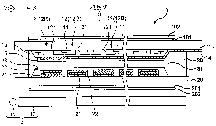
首先,参照图1说明将本实用新型应用于无源矩阵方式的半透射反射式液晶板的实施例。如图所示,液晶显示装置具有液晶板1和背光单元4。液晶板1的结构是相互相对的第1基板(上基板)10和第2基板(下基板)20通过密封材料30相互粘合,同时将例如TN(Twisted Nematic)型或STN(Super Twisted Nematic)型的液晶31封入到由两基板与密封材料30包围的区域中。背光单元4配置在液晶板1的第2基板20侧。以下,如图1所示的那样,对于液晶板1,将背光单元4的相反侧标记为「观察侧」。即,所谓「观察侧」,就是指观看该液晶板1的显示图像的观察者所在的一侧。First, an embodiment in which the present invention is applied to a transflective liquid crystal panel of a passive matrix system will be described with reference to FIG. 1 . As shown in the figure, the liquid crystal display device has a
背光单元4具有光源41和导光板42。光源41由例如LED(LightEmitting Diode)或冷阴极管等构成,向导光板42的侧端面照射光。导光板42是用于将入射到该侧端面上的光源41的光均匀地引导到液晶板1的基板面上的板状部件。另外,在导光板42中与液晶板1相对的面上,粘贴着用于将该导光板42的出射光向液晶板1均匀地扩散的扩散板,另一方面,在其相反侧的面上,粘贴着用于将从导光板42向液晶板1的相反侧传播的光向液晶板1侧反射的反射层(在图中都未示出)。光源41不是总是在点亮,在外光不充分的环境中使用时,根据用户的指示或传感器的检测信号而点亮。The
另一方面,液晶板1的第1基板10和第2基板20是玻璃或石英、塑料等具有光透过性的板状部件。其中,在第1基板10的外侧(液晶31的相反侧)表面上,粘贴了用于补偿干涉色的相位差板101和用于使入射光产生偏振的偏振光板102。在第2基板20的外侧(液晶31的相反侧)表面上,同样也粘贴了相位差板201和偏振光板202。On the other hand, the
在第1基板10的面上,设置了多个共用电极14。这里,图2是表示构成液晶板1的一部分要素的结构的平面图。从图2的A-A’线看的剖面图与图1对应。如图1和图2所示,各共用电极14是由ITO(IndiumTin Oxide)等透明导电材料形成的带状的电极,在图中所示的X方向延伸。A plurality of
另一方面,在第2基板20的面上,设置了多个分段电极22。各分段电极22和共用电极14一样,是由ITO等透明导电材料形成的带状的电极,如图1和图2所示,在与共用电极14交叉的方向(即图中的Y方向)延伸。如图1所示,形成共用电极14的第1基板10的表面和形成分段电极22的第2基板20的表面分别由取向膜15和23所覆盖。取向膜15和23是由例如聚酰亚铵等形成的有机薄膜,进行了用于规定未加电压时的液晶31的取向状态的摩擦处理。On the other hand, a plurality of
加在第1基板10与第2基板20之间的液晶31,其取向方向随加到共用电极14与分段电极22之间的电压而变化。下面,在本实施例中,如图2中的右下部分所示,将共用电极14与分段电极22相对的区域5标记为「点」。即,点5可以称为液晶31的取向方向根据所加的电压而变化的区域的最小单位。如图2所示,多个点5沿X方向和Y方向排列成矩阵状,各个点与红色(R)、绿色(G)、蓝色(B)中的某一种色对应。并且,由与这3色对应的3个点5R、5G、5B的组合构成与显示图像的最小单位相当的1个像素(子像素)。The alignment direction of the
其次,如图1所示,在第1基板10的内侧(液晶31侧)表面上,形成遮光层11、滤色片12和涂层13。其中,涂层13由例如聚丙烯酸类或环氧树脂类等树脂材料形成,起着使遮光层11和滤色片12的高低差实现平坦化的作用。上述共用电极14在该涂层13的表面形成。Next, as shown in FIG. 1, a light-
遮光层11形成为格子状,用以将排列成矩阵状的各点5的间隙(即,共用电极14与分段电极22相对的区域以外的区域)覆盖,起着将各点5的周围遮光的作用。该遮光层11由例如扩散了碳黑的黑色树脂材料或铬(Cr)等金属形成。The light-
其次,滤色片12(12R、12G、12B)是与各点5对应地形成的树脂层,分别利用染料或颜料着色了与点5的色对应的色,即红色(R)、绿色(G)、蓝色(B)中的某一色。因此,透过液晶31而向第1基板10传播的光中与各滤色片12的色对应的波长的光有选择地向观察侧出射。此外,在滤色片12上,如图1所示,与各点5的中央部附近对应地还设置了开口部121,关于这一点,后面进行说明。在本实施例中,表示出了采用经Y方向成列的多个点5排列同一色的滤色片12的结构(所谓的条形排列)的情况。Next, the color filter 12 (12R, 12G, 12B) is a resin layer formed corresponding to each
图3是表示在本实施例中使用的滤色片12的透射率特性的曲线图。在图3中,分别以向滤色片12入射的入射光的波长为横轴、以透射率(出射光量相对于入射光量的比率)为纵轴表示。如图所示,滤色片12R对与红色对应的约600nm以上的波长的光显示高的透射率,滤色片12G对与绿色对应的约500~600nm的波长的光显示高的透射率,滤色片12B对与蓝色对应的约400~500nm的波长的光显示高的透射率。并且,在图3的曲线图中,若比较各滤色片12的最大透射率时,可知红色的滤色片12R的最大透射率(约0.92)最大,蓝色的滤色片12B的最大透射率(约0.89)次之,绿色的滤色片12G的最大透射率最小。即,将同一光量的光照射各色的滤色片12时,从绿色的滤色片12G出射的光量比从红色的滤色片12R和蓝色的滤色片12B出射的光量少。FIG. 3 is a graph showing the transmittance characteristics of the
另一方面,如图1和图2所示,在第2基板20的内侧(液晶31侧)表面设置了多个反射层21。各反射层21是用于反射从第1基板10侧入射的入射光的层,是由例如铝或银等单体金属或以它们为主要成分的合金等形成的具有光反射性的薄膜。本实施例的反射层21是以银为主要成分而包含钯(Pd)和铜(Cu)的合金形成的。另外,为了在反射层21的表面形成散射构造(凹凸),第2基板20的内侧表面进行了粗糙化处理,但是,图示省略了。也可以采用使观察侧的偏振光板102具有散射特性的所谓的前方散射方式,取代在反射层21的表面形成散射构造的结构。On the other hand, as shown in FIGS. 1 and 2 , a plurality of
这里,图4是表示各反射层21与分段电极22的位置关系的图,是表示从图2的B-B’线看的剖面(即与分段电极22的延伸方向正交的剖面)的结构的图。如图所示,反射层21沿着与分段电极22正交的剖面的全部周边由分段电极22覆盖。更具体而言,如图4所示,构成分段电极22的一部分的第1层221在第2基板20的内侧表面上形成,同时,反射层21形成为将该第1层221中幅宽方向的一部分覆盖。此外,构成分段电极22的第2层222形成为从反射层21中与第2基板20平行的面到幅宽方向的周边部(边缘)将该反射层21覆盖。通过该结构,分段电极22与反射层21电连接。构成分段电极22的ITO的电阻值比较高,与此相反,构成反射层21的APC合金的电阻值比较低。因此,如图4所示,通过使分段电极22与反射层21接触,可以将配线电阻抑制低。Here, FIG. 4 is a diagram showing the positional relationship between each
另一方面,如图2所示,考虑与第2基板20的基板面平行的面时,多个反射层21都设置为与各点5的一部分重叠。此外,各反射层的全部周边位于点5内。换言之,各反射层21被各点5分离为岛状地设置在该点5内。On the other hand, as shown in FIG. 2 , considering a plane parallel to the substrate surface of the
并且,点5中与反射层21重叠的区域(以下,称为「反射区域51」)反射从第1基板10侧入射的光,起用于进行反射式显示的区域的功能。即,进行反射式显示时,从观察侧入射到液晶板1上的太阳光或室内照明光等外光在通过偏振光板102和相位差板101而成为指定的偏振状态之后,通过第1基板10→滤色片12→共用电极14→液晶31→分段电极22这样的路径到达反射层21,同时在其表面进行反射,然后沿原路返回。这时,由于液晶31的取向状态随共用电极14与分段电极22间的电压差而变化,所以,反射区域51的反射光中通过偏振光板102而被观察者所观察的光量就由各点5所控制。In addition, the region overlapping the
另一方面,点5中反射区域51以外的区域即点5中被反射层21所覆盖的区域以外的区域(以下,称为「透射区域」)52使从背光单元4入射到第2基板20上的光透过,起用于进行透射式显示的区域的功能。即,在点亮背光单元4的光源41进行透射式显示时,该背光单元4的照射光在通过偏振光板202和相位差板201而成为指定的偏振状态之后,通过第2基板20→(透射区域52→)分段电极22→液晶31→共用电极14→滤色片12→第1基板10这样的路径而向观察侧出射。在该透射式显示中,液晶31的取向状态也随共用电极14与分段电极22间的电压差而变化,所以,透过透射区域52的光中通过偏振光板102而被观察者所观察的光量由各点5所控制。On the other hand, the region other than the
下面,参照图5说明反射层21和滤色片12的更详细的结构。在图5中,仅图示出了构成1个像素的3色的点5。Next, a more detailed structure of the
如上所述,各点5具有与反射层21对应地反射从第1基板10侧入射的入射光的反射区域51和与该反射层21以外的区域对应地使从第2基板20侧入射的入射光透过到第1基板10侧的透射区域52。如图5所示,在各色的滤色片12上,在点5中与反射区域51对应的区域内设置了开口部121。开口部121是不设置滤色片12的部分,覆盖滤色片12和遮光层11的透明的涂层13进入该开口部121。在这样的结构中,进行反射式显示时,在反射层21的表面反射的光中透过滤色片12(开口部121以外的部分)的光由于该滤色片12的作用,光量将降低,相反,通过滤色片12的开口部121而向第1基板10侧出射的光由于仅透过透明的涂层13,所以,光量几乎不降低。因此,即使为了例如确保透射式显示时的色度而提高滤色片12的光透射率时(即,颜料或染料向滤色片12中的扩散量大时),也可以充分确保供反射式显示的光量,从而可以进行明亮的显示。这样,按照本实施例,可以同时确保反射式显示时的亮度和透射式显示时的色度。As described above, each
其次,在本实施例中,如图5所示,设置在滤色片12上的开口部121的面积随各色的滤色片12而异。即,设置在绿色的滤色片12G上的开口部121的面积比设置在红色的滤色片12R和蓝色的滤色片12B上的开口部121的面积大。这里,如参照图3以上所述的那样,绿色的滤色片12G的最大透射率比红色的滤色片12R和蓝色的滤色片12B的最大透射率低。即,各滤色片12的开口部121的面积是根据各滤色片12的透射率特性的不同而选定的。Next, in this embodiment, as shown in FIG. 5 , the area of the
此外,如图2和图5所示,反射区域51与透射区域52的面积比也随各滤色片12的透射率特性的不同而异。换言之,与各点5对应的反射层21的面积随该点5的色而异。具体而言,与绿色的点5G对应的反射区域51(或反射层21)的面积就比与红色和蓝色的点5R和5B对应的反射区域51(或反射层21)的面积大。In addition, as shown in FIG. 2 and FIG. 5 , the area ratio of the
这样,通过使滤色片12的开口部121的面积和反射层21的面积随各色的点5而异,可以补偿各滤色片12的透射率特性的差异,从而可以确保良好的显示品位。下面,详细说明该效果。In this way, by changing the area of the
首先,考虑设置在各滤色片12上的开口部121的面积。由于绿色的滤色片12G的最大透射率比其他色的滤色片12的最大透射率低,所以,如果对所有的滤色片12设置面积相等的开口部121,则透过绿色的滤色片12G的光量将比透过红色和蓝色的滤色片12R和12B的光量少。因此,在进行反射式显示时观察者对红色、绿色和蓝色的各色所观察的光量将有差别,从而难于实现良好的色再现性。与此相反,在本实施例中,由于在透射率低的绿色的滤色片12G上设置了面积比其他的滤色片12R和12B大的开口部121,所以,在进行反射式显示时,可以保持观察者对红色、绿色和蓝色的各色所观察的光量的平衡。First, the area of the
其次,考虑各点5的反射层21的面积。由于绿色的滤色片12G的最大透射率比其他色的滤色片12的最大透射率低,所以,如果对所有的色的点5使反射区域51的面积相等,则在与绿色的点5对应的反射层21的表面反射而向观察侧出射的光量就比在与其他色的点5对应的反射层21的表面反射而向观察侧出射的光量少,从而观察者所观察到的各色的光量将有差别。与此相反,在本实施例中,由于与绿色的点5G对应的反射层21的面积比其他的点5R和5B的反射层21的面积大,所以,可以充分确保在与绿色的点5G对应的反射层21的表面反射而向观察侧出射的光量。Next, the area of the
这样,按照本实施例,即使各色的滤色片12的透射率特性有差别时,也可以补偿该差别而实现良好的色再现性。Thus, according to this embodiment, even if the transmittance characteristics of the
在图5中,再次考虑各点5与该点5内的反射区域51和透射区域52的位置关系时,在本实施例中,反射区域51和透射区域52都与划定点5的4条边(即,构成点5的周边的4条边)中在Y方向延伸的一对边接近,同时,各区域沿该边而相邻。即,使略呈长方形的点5中的2条长边分别从该边的一端向另一端围过去时,,沿着该边各区域按透射区域52、反射区域51、透射区域52的顺序而相邻。换言之,如图5所示,在该点5内设想与点5的长边接近并且与该边平行的直线L时,该直线L将通过反射区域51和透射区域52。In Fig. 5, when considering again the positional relationship between each
这样,在本实施例中,与1个点5对应的反射区域51和透射区域52沿着该点5的周边而相邻,所以,对于该点5的反射区域51与透射区域52的面积比率,可以抑制发生由制造上的误差起因的偏差。详细情况,如以下所述。In this way, in this embodiment, the
作为在1个点5内包含反射区域51和透射区域52的结构,可以考虑例如图6(a)所示的结构。即,将反射层21形成为与各点5对应的反射层21的周边与该点5的周边不接近,换言之,仅透射区域52与各点5的周边接近。As a structure including a
这里,考虑制造这样结构的液晶板1的工序中将形成了反射层21的第2基板20与形成了遮光层11的第1基板10相互粘合的工序。在该工序中,通常是将两基板彼此间的相对位置对好,然后将该两基板相互粘贴。这时,假定由于例如制造技术上的理由等原因而两基板在X方向上的相对位置发生了偏离时,如图6(b)所示,点5中的透射区域52的一部分将被遮光层11所覆盖。这样,被遮光层11所覆盖的部分就不能对显示有贡献,所以,透射区域在点5中所占的面积就比适当地配置遮光层11时(即图6(a)的情况)小。另一方面,由于反射区域51与区域的周边不接近,所以,即使发生这样的基板偏离时,反射区域51也不会被遮光层11所覆盖。即,反射区域在点5中所占的面积与图6(a)所示的情况没有变化。这样,在图6所示的结构中,透射区域52的面积虽然会由于基板相互粘贴的误差而减小,但是,反射区域51的面积却不变,所以,反射区域51与透射区域52的面积比率将与所期望的面积比率不同。结果,透射式显示的亮度将比反射式显示时暗,从而亮度将随显示方式而发生偏差。Here, a step of bonding the
与此相反,在本实施例中,反射区域51和透射区域52在确定1个点5的多条边的附近沿该边相邻。因此,第1基板10与第2基板20的相对位置从图7(a)所示的适当的位置(设计上的位置)看向X方向偏离时,如图7(b)所示,反射区域51的面积也与透射区域52的面积一起减小。即,按照本实施例,即使反射层21与遮光层11的相对位置发生了偏离时,也可以避免只减小透射区域52或反射区域51的某一方的面积,所以,可以抑制反射区域51与透射区域52的面积比率偏离所期望的值。On the contrary, in the present embodiment, the
实施例2.Example 2.
下面,说明本实用新型实施例2的液晶板。Next, the liquid crystal panel of Embodiment 2 of the present invention will be described.
在上述实施例1中,给出了在位于观察侧的第1基板10上设置了遮光层11、滤色片12和涂层13的结构。与此相反,在本实施例中,则是将这些要素设置在第2基板20上。In the first embodiment described above, the structure in which the light-
图8是表示本实施例的液晶板的结构的剖面图,图9是表示该液晶板上的点、滤色片和反射层的位置关系的平面图和剖面图。对于图8和图9所示的各结构要素中与上述实施例1的液晶板的结构要素共同的部分标以相同的符号。8 is a cross-sectional view showing the structure of the liquid crystal panel of this embodiment, and FIG. 9 is a plan view and a cross-sectional view showing the positional relationship of dots, color filters, and reflective layers on the liquid crystal panel. Among the constituent elements shown in FIG. 8 and FIG. 9 , the same reference numerals are assigned to the same parts as the constituent elements of the liquid crystal panel of the first embodiment described above.
如图8和图9所示,在第2基板20的面上形成分别与点5对应的多个反射层21。这些反射层21与上述实施例1所示的相同。即,如图9所示,反射层21分别在点5的周边的内侧形成,其形状选定为沿着各点5的周边使反射区域51与透射区域52相邻,并且,与绿色的点5G对应的反射层21的面积比与其他色的点5R和5B对应的反射层21的面积大。As shown in FIGS. 8 and 9 , a plurality of
并且,在形成了多个反射层21的第2基板20的面上,设置了与点5的间隙重叠的遮光层11和着色为各点5的色的滤色片12(12R、12G、12B)。如图9所示,在各滤色片12中与反射区域51对应的区域内设置了开口部121。和上述实施例1一样,各开口部121的面积因各色的点5而异。即,如图9所示,与绿色的点5G对应的开口部121的面积比与红色和蓝色的点5R和5B对应的开口部121的面积大。And, on the surface of the
此外,设置了反射层21、遮光层11和滤色片12的第2基板20的表面被涂层13所覆盖,在该涂层13的表面形成分段电极22。该分段电极22由与图4所示的结构(由第1层221和第2层222构成的结构)不同的单层的透明导电材料构成。并且,设置了分段电极22的涂层13的表面被取向膜23所覆盖。In addition, the surface of the
另一方面,如图8所示,在第1基板10的内侧表面形成共用电极14,该共用电极14被取向膜15所覆盖。在图9的剖面图中,省略了第1基板10上的各要素的图示。On the other hand, as shown in FIG. 8 , a
利用这样在第2基板20上设置遮光层11和滤色片12的结构,也可以得到和上述实施例1同样的效果。即,如上述实施例1和实施例2所示,不论在位于观察侧的第1基板10和位于背面侧的第2基板20中的某一基板上是否设置了滤色片12,都可以应用本实用新型。通常遮光层11或滤色片12是使用光刻或腐蚀技术等以比较高的精度形成的,所以,与在第1基板10上形成遮光层11的情况相比,可以说反射层21与遮光层11的相对位置难于发生偏离。考虑到该情况,可以抑制参照图6和图7说明的反射区域51与透射区域52的面积比率的误差的优点,在第1基板10上形成遮光层11(和滤色片12)时可以特别显著地表现出来。The same effect as that of the above-mentioned first embodiment can be obtained also by the structure in which the light-
[变形例][modified example]
以上,说明了实施例1和实施例2,上述实施例都是示例,对于上述实施例,在不脱离本实用新型的主旨的范围内可以进行各种各样的变形。作为变形例,可以考虑例如以下的例子。As mentioned above, although Example 1 and Example 2 were demonstrated, the said Example is an example, Various deformation|transformation is possible about the said Example in the range which does not deviate from the summary of this invention. As modifications, for example, the following examples can be considered.
变形例1.
在上述实施例1和实施例2中,为了补偿各色的滤色片12的透射率特性的差异,使与绿色的点5G对应的反射层21的面积和滤色片12G的开口部121的面积与和红色的点5R和蓝色的点5B对应的这些面积不同,但是,对于红色、绿色和蓝色的各色,也可以使这些面积不同。另外,在上述各实施例中,使与各色的点对应的反射层21的面积和滤色片12的开口部121的面积随滤色片12的透射率特性而不同,但是,也可以使之随背光单元的照射光的分光特性而不同。即,在例如与蓝色对应的波长的光量比与绿色和红色对应的波长的光量小时,在背光单元4的照射光的分光特性有偏差时,通过使与蓝色的点5B对应的反射层21的面积小于与其他色的点5对应的反射层21的面积,也可以充分确保该点5B的透射区域。这样,用于决定与各点5对应的反射层21的面积和滤色片12的开口部121的面积的要素就不限于滤色片12的透射率特性。另一方面,在本实用新型中,不一定必须使各点5的反射层21的面积和滤色片12的开口部121的面积不同。In the first and second embodiments described above, in order to compensate for the difference in transmittance characteristics of the
变形例2.Variation 2.
在上述实施例1中,如图4所示,给出了使反射层21与分段电极22接触的结构,但是,也不一定必须使它们接触。即,如图10所示,也可以采用利用由树脂材料等构成的绝缘层25将设置了反射层21的第2基板20的表面所覆盖同时在该绝缘层25的表面设置了由透明导电膜的单层构成的分段电极2的结构。In the above-mentioned
变形例3.Variation 3.
在上述实施例1和实施例2中,给出了不具有开关元件的无源矩阵方式的液晶板,但是,对于具有以TFD(Thin Film Diode)为代表的二端子型开关元件或以TFT(Thin Film Transistor)为代表的三端子型开关元件的有源矩阵方式的液晶板,也可以和上述实施例一样应用本实用新型。另外,在上述各实施例中,给出了采用同一色的滤色片12排成一列的条形排列的情况,但是,作为滤色片12的排列的形式,也可以采用镶嵌排列或三角形排列。In the above-mentioned
实施例3.Example 3.
下面,说明实施例3。实施例3的液晶显示装置是无源矩阵方式的半透射反射式彩色液晶显示装置的例子。图11是表示实施例3的液晶显示装置的概略结构的剖面图,图12是表示将构成显示区域的多个像素放大表示的平面图。Next, Example 3 will be described. The liquid crystal display device of Example 3 is an example of a passive matrix transflective color liquid crystal display device. 11 is a cross-sectional view showing a schematic configuration of a liquid crystal display device according to Example 3, and FIG. 12 is an enlarged plan view showing a plurality of pixels constituting a display area.
如图11所示,实施例3的液晶显示装置1001具有液晶单元1002和后照明灯1003(照明单元)。液晶单元1002由下基板1004和上基板1005通过密封材料1006相对配置并将由STN(Super Twisted Nematic)液晶等构成的液晶层1007封入由上基板1005、下基板1004和密封材料1006包围的空间而成,在液晶单元1002的后面侧(下基板的外面侧)配置了背光1003。As shown in FIG. 11, a liquid
在由玻璃或塑料等透射性材料构成的下基板1004的内面侧,在由铝或其合金、银或其合金等光反射率高的金属膜构成的反射膜1008上,层叠了铟锡氧化物(Indium Tin Oxide,以下,略记为ITO)等透明导电膜1009的2层结构的分段电极1010在贯穿纸面的方向形成为条形。并且,在其上形成对表面进行了例如摩擦处理的由聚酰亚铵等构成的取向膜1011。本实施例的情况是,分段电极1010的结构不仅在反射膜1008的上面层叠透明导电膜1009,而且为了使透明导电膜1009将反射膜1008的侧面也覆盖,将透明导电膜1009的图形宽度设定得大于反射膜1008的图形宽度。On the inner surface of the
另一方面,在由玻璃、塑料等透射性材料构成的上基板1005的内面侧,形成具有红(R)、绿(G)、蓝(B)的各着色层1013R、1013G、1013B和将这些不同色的着色层1013R、1013G、1013B间区划开的遮光部1014(黑色矩阵)的滤色片1015。遮光部1014由例如树脂黑或反射率比较低的铬等金属形成。并且,在滤色片1015上,在将各着色层1013R、1013G、1013B间的高低差进行平坦化处理的同时,形成用于保护各着色层1013R、1013G、1013B的表面的涂膜1016。该涂膜1016可以是聚丙烯酸类、聚酰亚铵等树脂膜,也可以是氧化硅膜等无机膜。此外,在涂膜1016上,由ITO等单层膜构成的共用电极1017在与纸面平行的方向形成为条形,并在其上形成对表面进行了例如摩擦处理的由聚酰亚铵等构成的取向膜1018。On the other hand,
在下基板1004的外面侧,从基板侧开始顺序设置了相位差板1020和偏振光板1021,此外,在偏振光板1021的外面侧设置了背光1003。背光1003具有冷阴极管、发光二极管(Light Emitting Diode,LED)等光源1002、反射板1023和导光板1024。另外,在上基板1005的外面侧,从基板侧开始顺序设置了相位差板1025和偏振光板1026。On the outer side of the
各基板1004、1005上的电极的配置如图12所示,在下基板1004上,沿图12的纵向延伸的多个分段电极1010形成为条形。另一方面,在上基板1005上,与分段电极1010正交地在图12的横向延伸的多个共用电极1017形成为条形。滤色片1015的R、G、B的各着色层1013R、1013G、1013B与各分段电极1010的延伸方向对应地配置。即,本实施例的滤色片1015是被称为所谓的纵条形的图形,R、G、B的着色层1013R、1013G、1013B分别纵向以同色配置为条形。这样,就构成了由在图12所示的横向排列的R、G、B的3个点1028R、1028G、1028B构成显示图形的1个像素1029。所谓点,就是各分段电极1010与各共用电极1017交叉的部分,是显示的最小单位部分。The arrangement of the electrodes on the
在本实施例中,由反射膜1008和透明导电膜1009构成的2层结构的层叠膜构成分段电极1010,这些膜中,反射膜1008在反射模式时起对显示有贡献的反射膜的功能。反射膜1008和透明导电膜1009都在图12的纵向延伸,但是,反射膜1008的图形与透明导电膜1009的图形的宽度不同,如上所述,将透明导电膜1009的图形宽度形成为大于反射膜1008的图形宽度。这样,在各点1028R、1028G、1028B内,中央部就是存在反射膜1008和透明导电膜1009的区域,该区域在半透射反射式液晶显示装置中就是反射模式的反射区域R。另外,在反射区域R的两侧是仅存在透明导电膜1009的区域,该区域在半透射反射式液晶显示装置中是透射模式的透射区域T。即,在各点1028R、1028G、1028B内,反射区域R和透射区域T都存在。In this embodiment, the
此外,在本实施例中,反射膜1008的图形宽度不固定,在各点1028R、1028G、1028B的中央部,设置了宽度比主线条部分宽的扩幅部1008a。另一方面,上基板1005上的滤色片1015的R、G、B的各着色层1013R、1013G、1013B不是在遍及各点1028R、1028G、1028B内的整个面上设置,对于各着色层1013R、1013G、1013B,在各点1028R、1028G、1028B上设置了开口部(图12中用留白表示的部分)。即,该开口部是非着色区域1031R、1031G、1031B,特别是非着色区域1031R、1031G、1031B在与反射膜1008的扩幅部1008a平面重叠的区域内,设置为收容在扩幅部1008a中。即,非着色区域1031R、1031G、1031B是仅存在反射膜1008和透明导电膜1009的区域,非着色区域以外的反射区域R是存在反射膜1008、透明导电膜1009和滤色片的着色层1013R、1013G、1013B的区域,透射区域T是存在透明导电膜1009和着色层1013R、1013G、1013B的区域。在本实施例中,扩幅部1008a的形状略为长方形,非着色区域1031R、1031G、1031B的形状也略为长方形。In addition, in this embodiment, the width of the pattern of the
在上述结构的液晶显示装置1001中,反射模式时从上基板1005侧入射的外光的一部分透过反射区域R内的非着色区域1031R、1031G、1031B,在反射模式时2次透过滤色片1015而得到的光与透过非着色区域1031R、1031G、1031B而未着色的光和透过着色区域而着色的光重叠。另一方面,在透射模式时从背光1003透过该透射区域T的光全部透过着色区域,所以,在透射模式时通过1次透过滤色片1015而得到的光全是着色的光。这样,便可减小在反射模式时2次透过滤色片1015而得到的光与在透射模式时1次透过滤色片1015而得到的光的色的浓淡差,通过使滤色片1015的着色层1013R、1013G、1013B达到最佳状态,便可得到不论在反射模式时还是透射模式时都发色良好而视认性高的显示。In the liquid
另外,在本实施例中,用透明导电膜1009和反射膜1008的2层结构的层叠膜构成分段电极1010,所以,由于位于透射区域T的透明导电膜1009的存在,可以毫无障碍地将电场加到透射区域T上的液晶层1007上,同时,由于由电阻率比透明导电膜1009小的金属构成的反射膜1008的存在,可以降低分段电极1010全体的电阻值。In addition, in this embodiment, the
下面,说明普通实施上述实施例1的结构的液晶显示装置时容易发生非着色区域的面积的偏差或反射区域与非着色区域的对准偏差等问题的理由。Next, the reasons why problems such as variation in the area of the non-colored region and misregistration between the reflective region and the non-colored region tend to occur when the liquid crystal display device having the structure of the above-mentioned
作为前提,和本实施例一样,反射膜构成条形的电极的一部分。这时,如上所述,在可以得到降低电极的电阻值等效果方面是理想的,但是,反射膜也必须成形为条形的。实施例1的液晶显示装置在各点内设置了反射区域和透射区域,所以,在采用例如用反射膜将点全体覆盖的形状的基础上,也可以考虑在反射膜上设置光透过用的窗部(透射区域)。但是,如上所述,不论如何,反射膜也成形为条形,所以,如果将金属膜图形的宽度相对于透明导电膜图形的宽度设计得窄,则其两侧自然就成为透射区域,所以,在设计上这就比专门设置窗部简单。As a premise, as in the present embodiment, the reflective film constitutes a part of the strip-shaped electrode. In this case, as described above, it is desirable because the effect of reducing the resistance value of the electrode can be obtained, but the reflective film must also be formed in a stripe shape. In the liquid crystal display device of
即,按照最简单的图形设计,如图23所示,相对于构成分段电极1110的带状的透明导电膜1109的图形宽度,就减小了带状的反射膜1108的图形宽度。此外,实施例1的液晶显示装置在反射区域内设置了非着色区域,所以,在反射膜1108上设置不存在滤色片的着色层的非着色区域1131(着色层的开口部)。如图23所示,在彩色用的液晶显示装置中,通常点1128本身是纵长的长方形,所以,反射区域R的形状也成为纵长的,此外,非着色区域1131也成为纵长的长方形。That is, according to the simplest pattern design, as shown in FIG. 23 , the pattern width of the strip-shaped
这样,要实现实施例1的液晶显示装置时,着色层的开口部(非着色区域)自然就成为纵长的长方形,越增大开口部的面积,就越成为纵向细长的长方形。使用光刻技术形成具有这种形状的开口部的着色层时,发生了腐蚀尺寸的偏差时,开口部面积的偏差将增大。其理由在于,例如同一面积的正方形图形与长方形图形相比,发生了相同的腐蚀尺寸误差时,长方形图形的面积变化将大于正方形图形,在长方形图形中,越是细长的长方形,面积的变化就越大。结果,反射模式时的亮度和色相等显示特性的偏差将增大。另外,如果开口部的宽度太细,超过了光刻技术的解像度的极限时,就不能形成开口部。In this way, when realizing the liquid crystal display device of Example 1, the opening (non-colored region) of the colored layer naturally becomes a vertically elongated rectangle, and the larger the area of the opening, the more vertically elongated the rectangle becomes. When a colored layer having such an opening is formed using a photolithography technique, if a variation in the etching size occurs, the variation in the area of the opening increases. The reason is that, for example, when the same corrosion size error occurs between a square figure and a rectangular figure with the same area, the area change of the rectangular figure will be larger than that of the square figure. bigger. As a result, variations in display characteristics such as luminance and hue in reflective mode increase. In addition, if the width of the opening is too narrow and exceeds the resolution limit of the photolithography technique, the opening cannot be formed.
另外,例如在下基板上形成反射膜而在上基板上形成滤色片时,为了将非着色区域形成为确实收容在反射区域内,反射膜的图形与滤色片的图形的对准精度即下基板与上基板相互粘贴时的对准精度就很重要。然而,要在长方形的反射区域中配置具有某种程度的面积的长方形的非着色区域时,无论怎样,反射区域的短边方向的边缘与非着色区域的短边方向的边缘间的间隔将变窄,从而对准的余量将减小。因此,考虑了通过设计使上述反射区域的边缘与非着色区域的边缘的间隔小于基板相互粘贴时的对准误差的情况,这时,非着色区域发生向透射区域内突出时,将不能完全得到所希望的光学特性。In addition, for example, when a reflective film is formed on the lower substrate and a color filter is formed on the upper substrate, in order to form the non-colored area so as to be accommodated in the reflective area reliably, the alignment accuracy of the pattern of the reflective film and the pattern of the color filter is lower. The alignment accuracy when the substrate and the upper substrate are attached to each other is very important. However, when a rectangular non-colored region having a certain area is arranged in a rectangular reflective region, the distance between the short-side edges of the reflective region and the short-side edges of the non-colored region will be reduced. Narrow, so the margin for alignment will be reduced. Therefore, it is considered that the distance between the edge of the reflective area and the edge of the non-colored area is smaller than the alignment error when the substrates are pasted together by design. At this time, when the non-colored area protrudes into the transmissive area, it will not be completely obtained. desired optical properties.
与此相反,在图12所示的本实施例的液晶显示装置中,通过采用在各点1028R、1028G、1028B中设置反射膜1008的扩幅部1008a、而且将非着色区域1031R、1031G、1031B配置到与扩幅部1008a平面重叠的区域的结构,配置非着色区域1031R、1031G、1031B的反射区域R的部分的形状就成为比以往的形状更接近正方形。这样,就可以将发生一定的腐蚀尺寸误差时的开口部面积的偏差抑制得比原来的小,所以,可以降低反射模式时的显示特性的偏差。此外,使配置非着色区域1031R、1031G、1031B的反射区域R的部分比以往的形状更接近正方形时,就可以使反射区域R的边缘与非着色区域1031R、1031G、1031B的边缘的间格G比以往的间隔宽,所以,对准的余量将增大,从而成为对粘贴偏离适应性强的结构,同时也容易得到所希望的光学特性。On the contrary, in the liquid crystal display device of this embodiment shown in FIG. In the structure arranged in a region overlapping with the expanding
实施例4.Example 4.
下面,参照附图说明本实用新型的实施例4。Next,
图13是将构成实施例4的液晶显示装置的显示区域的多个像素放大表示的平面图,是与实施例3的图12相当的图。本实施例的液晶显示装置的基本结构与实施例3相同,仅反射区域和非着色区域的形状与实施例3不同。在图13中,对于与图12相同的结构要素标以相同的符号,并省略其详细的说明。13 is an enlarged plan view of a plurality of pixels constituting the display area of the liquid crystal display device of the fourth embodiment, and is a view corresponding to FIG. 12 of the third embodiment. The basic structure of the liquid crystal display device of this embodiment is the same as that of Embodiment 3, and only the shape of the reflective region and the non-colored region is different from that of Embodiment 3. In FIG. 13 , the same reference numerals are assigned to the same constituent elements as those in FIG. 12 , and detailed description thereof will be omitted.
在实施例3中,在与R、G、B的不同色对应的各点中,反射区域的面积和形状、非着色区域的面积和形状是相同的,与此相反,在本实施例中,在与R、G、B的不同色对应的各点间,至少1个的反射区域的面积、非着色区域的面积分别不同,相应地反射区域的形状、非着色区域的形状也不同。In Example 3, the area and shape of the reflective area and the area and shape of the non-colored area are the same at each point corresponding to the different colors of R, G, and B. On the contrary, in this example, Between dots corresponding to different colors of R, G, and B, the area of at least one reflective region and the area of the non-colored region are different, and the shape of the reflective region and the shape of the non-colored region are also different accordingly.
具体而言,如图13所示,例如在不同色的点1028R、1028G、1028B间,G的点1028G的反射区域R的面积最大,B的点1028B的反射区域R次之,R的点1028R的反射区域R最小。换言之,G的点1028G的透射区域T的面积最小,B的点1028B的透射区域T次之,R的点1028R的透射区域T最大。另外,G的点1028G的非着色区域1031G的面积最大,R的点1028R的非着色区域1031R次之,B的点1028B的非着色区域1031B最小。Specifically, as shown in FIG. 13 , for example, among the
按照本实施例的液晶显示装置,可以对R、G、B的各色调整反射率和反射模式时的各色光的色度、透射率和透射模式时的各色光的色度,所以,可以适当地调整反射模式时的显示的亮度和色度(例如白显示时的色相)以及透射模式时的显示的亮度和色度(例如白显示时的色相)。这样,便可使反射模式时和透射模式时的显示品位平衡良好而最佳化。According to the liquid crystal display device of this embodiment, each color of R, G, and B can adjust the reflectivity and the chromaticity of each color light during the reflection mode, the transmittance and the chromaticity of each color light during the transmission mode, so it can be suitably The brightness and chromaticity of the display in the reflective mode (for example, the hue of the white display) and the brightness and chromaticity of the display in the transmissive mode (for example, the hue of the white display) are adjusted. In this way, the display quality in the reflective mode and in the transmissive mode can be well-balanced and optimized.
更具体而言,将G的点1028G的透射区域T的面积设定为小于R、B的点1028R、1028B的透射区域T的面积,但是,由于绿色光比红色光和蓝色光具有充分高的视觉灵敏度,所以,这样设定不会影响色平衡,而且可以维持充分的透射率。另外,将G的点1028G的非着色区域1031G的面积设定为大于R、B的点1028R、1028B的非着色区域1031R、1031B的面积,所以,可以提高反射模式的反射率和色再现性。More specifically, the area of the transmissive region T of the
在上述实施例3和实施例4中,给出了反射膜的扩幅部的形状略为长方形、非着色区域的形状也是略为长方形的例子,但是,这些部分的形状并不特别限定长方形。例如,也可以如图14所示的那样,使扩幅部1008b的形状为略呈六角形,相应地也使非着色区域1031b的形状为略呈六角形,或者,也可以如图15所示的那样,使扩幅部1008c的形状为略呈椭圆形,相应地使非着色区域1031c的形状也为略呈椭圆形。In the above-mentioned Examples 3 and 4, examples were given in which the shape of the widening portion of the reflective film is approximately rectangular, and the shape of the non-colored region is also approximately rectangular. However, the shapes of these portions are not particularly limited to rectangles. For example, as shown in FIG. 14, the shape of the expanding
另外,在上述实施例中,举出了在反射膜上层叠透明导电膜而构成2层结构的电极的例子,但是,在本实用新型中,起反射膜功能的金属膜可以不一定构成电极,作为绝缘膜介于金属膜与透明导电膜之间的结构,金属膜可以专门仅起反射膜的功能。但是,这时,在本实用新型中金属膜必须形成为条形。另外,在上述实施例中,举出了滤色片的图形为纵条形的例子,但是,除此之外,本实用新型也可以应用于横条形排列、镶嵌排列、三角形排列等的滤色片。此外,不限于在上述实施例中所示的无源矩阵型液晶显示装置,也可以将本实用新型应用于以TFD作为开关元件的有源矩阵型液晶显示装置。In addition, in above-mentioned embodiment, enumerated the example that laminates transparent conductive film on reflective film and constitutes the electrode of two-layer structure, but, in the present utility model, the metal film that plays reflective film function can not necessarily form electrode, As a structure in which an insulating film is interposed between a metal film and a transparent conductive film, the metal film may exclusively function only as a reflective film. However, at this time, the metal film must be formed in a stripe shape in the present invention. In addition, in the above-mentioned embodiment, the example of the pattern of the color filter is a vertical strip, but, in addition, the utility model can also be applied to the filter of the horizontal strip arrangement, mosaic arrangement, triangular arrangement, etc. color chips. In addition, it is not limited to the passive matrix liquid crystal display device shown in the above-mentioned embodiments, and the present invention can also be applied to an active matrix liquid crystal display device using TFD as a switching element.
[实施例][Example]
其次,本实用新型者在本实用新型的液晶显示装置中改变各种参量进行反射率、透射率、显示色等的光学特性的模拟,证实了本实用新型的效果,下面,报告该结果。Next, the inventors of the present invention changed various parameters in the liquid crystal display device of the present invention to simulate optical characteristics such as reflectance, transmittance, display color, etc., and verified the effect of the present invention. The results are reported below.
作为模拟的前提条件,取点数为120×3(R、G、B)(横)×160(纵)、横向的点间距为85μm、纵向的点间距为225μm。图16~图19表示以下所示的结构例1~3的G的点的各部分的尺寸,图20表示以下所示的结构例3的像素内的各部分的尺寸。这些图中符号B所示的区域(画网格的区域)是点间的黑色矩阵,取在横向延伸的黑色矩阵宽度为13μm、在纵向延伸的黑色矩阵宽度为9μm。这样,各点间距的面积(包含黑色矩阵)就是21675μm2,各点的面积(不包含黑色矩阵)就是18392μm2。另外,滤色片就使用具有图21所示的分光特性的滤色片。As the preconditions for the simulation, the number of points is 120×3 (R, G, B) (horizontal)×160 (vertical), the horizontal point pitch is 85 μm, and the vertical point pitch is 225 μm. FIGS. 16 to 19 show the dimensions of each part of the G dot in the configuration examples 1 to 3 shown below, and FIG. 20 shows the dimensions of each part in the pixel of the configuration example 3 shown below. The area indicated by symbol B in these figures (the area where the grid is drawn) is a black matrix between dots, and the width of the black matrix extending in the lateral direction is 13 μm, and the width of the black matrix extending in the vertical direction is 9 μm. In this way, the area of each dot pitch (including the black matrix) is 21675 μm 2 , and the area of each dot (excluding the black matrix) is 18392 μm 2 . In addition, as a color filter, a color filter having the spectral characteristics shown in FIG. 21 is used.
结构例1.Structure example 1.
在结构例1中,在R、G、B所有的点中,将1点内的透射区域的面积采用与8712μm2相同的值。另外,在R、B的点中,将1点内的非着色区域的面积取为360μm2,与此相对,仅将G的点设定为大到2161μm2。通过模拟计算了这时的反射率、反射模式时的色域面积和白显示色、透射率、透射模式时的色域面积(表示色的色度,是在xy坐标系中连结红、绿、蓝显示的各坐标的三角形的面积)和白显示色。色域面积、白显示色都是根据xyY色表系统色度图表示的值。上述光学特性值示于以下的「表1」。In Structural Example 1, at all the dots R, G, and B, the area of the transmissive region within one dot is set to the same value as 8712 μm 2 . In the R and B points, the area of the non-colored region within one point was set to 360 μm 2 , whereas only the G point was set to be as large as 2161 μm 2 . The reflectance at this time, the color gamut area in reflective mode and white display color, transmittance, and the color gamut area in transmissive mode were calculated by simulation (expressing the chromaticity of the color, which is connected in the xy coordinate system to red, green, and The area of the triangle for each coordinate displayed in blue) and the color displayed in white. The color gamut area and white display color are all values represented by the chromaticity diagram of the xyY color table system. The above-mentioned optical characteristic values are shown in the following "Table 1".
结构例2.Structure example 2.
在结构例2中,与结构例1不同,对各点改变1点内的透射区域的面积。即,在G的点内最小,取为6776μm2,在B的点内次之,取为10406μm2,在R的点内最大,取为11130μm2。另外,将1点内的非着色区域的面积在R的点内设定为180μm2、在G的点内设定为3240μm2。在B的点内不设置非着色区域。通过模拟计算了这时的反射率、反射模式时的色域面积和白显示色、透射率、透射模式时的色域面积和白显示色。这些光学特性值示于以下的「表1」。In Structural Example 2, unlike Structural Example 1, the area of the transmissive region within one dot is changed for each dot. That is, the smallest point in G is 6776 μm 2 , the second largest point in B is 10406 μm 2 , and the largest point in R is 11130 μm 2 . In addition, the area of the non-colored region in one point was set to 180 μm 2 in the R point and 3240 μm 2 in the G point. No non-colored area is set within the point of B. The reflectance at this time, the color gamut area and white display color in reflective mode, the transmittance, the color gamut area and white display color in transmissive mode were calculated by simulation. These optical characteristic values are shown in "Table 1" below.
结构例3.Structure example 3.
在结构例3中,使用具有图22所示的分光特性的滤色片取代具有图21的分光特性的滤色片。将图21和图22的分光特性比较可知,各色的曲线的峰值部分(透射区域)几乎没有变化,但是,峰值以外的区域(吸收区域)的透射率水平则是图21高而图22低。换言之,在结构例3中,与结构例2相比,使用了色纯度高的滤色片。伴随该滤色片的变更,1点内的透射区域的面积、非着色区域的面积分别随各点而少许发生了变化。通过模拟计算了这时的反射率、反射模式时的色域面积和白显示色、透射率、透射模式时的色域面积和白显示色。这些光学特性值示于以下的「表1」。In Structural Example 3, a color filter having the spectral characteristic shown in FIG. 22 is used instead of the color filter having the spectral characteristic shown in FIG. 21 . Comparing the spectral characteristics in Fig. 21 and Fig. 22, it can be seen that there is almost no change in the peak portion (transmission region) of the curves of each color, but the transmittance level of the region other than the peak (absorption region) is higher in Fig. 21 and lower in Fig. 22 . In other words, in Structural Example 3, compared with Structural Example 2, a color filter with higher color purity is used. With the change of the color filter, the area of the transmissive region and the area of the non-colored region in one dot slightly changed for each dot. The reflectance at this time, the color gamut area and white display color in reflective mode, the transmittance, the color gamut area and white display color in transmissive mode were calculated by simulation. These optical characteristic values are shown in "Table 1" below.
表1
各结构例的光学特性如表1所示,首先,实现结构例1的各部分的面积的反射区域和非着色区域的图形尺寸使用现有的直线的带状反射区域时,则成为例如图16所示的那样。以下图16~图20中的数值是用μm单位表示的尺寸。并且,使用反射区域具有扩幅部的本实用新型的结构实现结构例1的各部分的面积即与图16相同的各部分的面积时,就成为例如图17所示的那样。The optical characteristics of each structural example are shown in Table 1. First, when the pattern size of the reflective region and the non-colored region of the area of each part realizing the structural example 1 is used in the existing linear band-shaped reflective region, it becomes, for example, Fig. 16 as shown. The numerical values in Fig. 16 to Fig. 20 below are dimensions expressed in units of μm. And, when the area of each part of the configuration example 1, that is, the same area of each part as in FIG. 16 is realized using the structure of the present invention in which the reflection region has an expanding portion, it becomes, for example, as shown in FIG. 17 .
这里,考虑在纵向延伸的反射区域的边缘与非着色区域的边缘间的间隔,在图16的结构中是15μm。在液晶显示装置的制造工艺中,上基板与下基板相互粘合时的对准误差按现在的水平约为15μm,所以,若考虑在上基板与下基板相互粘贴时发生最大的偏离时,则调整的余量就完全没有了。与此相反,在图17的结构中,反射区域的边缘与非着色区域的边缘间的间隔为18.7μm。因此,这时,在上基板与下基板相互粘贴时即使发生了最大的偏离,也仍然有约3.7μm的余量。这样,就证实了按照本实用新型的结构,可以实现对相互粘贴偏离适应性强的结构。Here, considering the interval between the edge of the reflective region extending in the longitudinal direction and the edge of the non-colored region, it is 15 μm in the structure of FIG. 16 . In the manufacturing process of liquid crystal display devices, the alignment error when the upper substrate and the lower substrate are bonded to each other is about 15 μm at the current level. Therefore, if the largest deviation occurs when the upper substrate and the lower substrate are bonded to each other, then There is absolutely no margin for adjustment. In contrast, in the structure of FIG. 17, the interval between the edge of the reflective region and the edge of the non-colored region was 18.7 μm. Therefore, at this time, even if the maximum deviation occurs when the upper substrate and the lower substrate are attached to each other, there is still a margin of about 3.7 μm. In this way, it has been confirmed that according to the structure of the utility model, a structure with strong adaptability to mutual sticking deviation can be realized.
此外,考虑非着色区域的横尺寸时,在图16中是10μm,在图17是18.6μm。例如,假定制造液晶显示装置所使用的光刻技术的解像度约为10μm时,在图16中是勉强可以形成开口部(非着色区域)的值,可以认为有时将不能实现。与此相反,在图17的结构中,可以可靠而高精度地形成非着色区域。In addition, when the lateral size of the non-colored region is considered, it is 10 μm in FIG. 16 and 18.6 μm in FIG. 17 . For example, assuming that the resolution of the photolithography technology used to manufacture the liquid crystal display device is about 10 μm, the opening (non-colored region) can be barely formed in FIG. 16 , and it may not be possible. In contrast, in the structure of FIG. 17, the non-colored region can be formed reliably and with high precision.
另外,若考虑表1中结构例1的光学特性中的「透射模式时的白显示色」时,x=0.314、y=0.347,表示白中略带红色的情况。因此,为了使透射模式时的白显示色更白,调整了各部分的面积的就是结构例2。因此,具体而言,就是将G的透射区域的面积比结构例1大大减小,即使这样,为了维持与结构例1同等的透射率,分别增加R和B的透射区域的面积。并且,相反,由于增加了G的反射区域的面积,所以,为了抑制反射光中的G的成分,也将G的非着色区域的面积比结构例1增大了。伴随该变更,为了维持反射率和反射时的色,也调整了R和B的非着色区域的面积。In addition, considering the "white display color in transmission mode" in the optical characteristics of Structural Example 1 in Table 1, x=0.314 and y=0.347, indicating a reddish white. Therefore, in order to make the white display color in the transmissive mode even whiter, the area of each part is adjusted, which is the configuration example 2. Therefore, specifically, the area of the transmissive region of G is much smaller than that of Structural Example 1. Even so, in order to maintain the same transmittance as that of Structural Example 1, the areas of the R and B transmissive regions are respectively increased. And, conversely, since the area of the reflection region of G is increased, the area of the non-colored region of G is also larger than that of the first configuration in order to suppress the G component in the reflected light. Along with this change, in order to maintain the reflectance and color at the time of reflection, the areas of the non-colored regions of R and B are also adjusted.
使用反射区域具有扩幅部的本实用新型的结构实现结构例2的各部分的面积时,就成为例如图18所示的那样。在该结构中,反射区域的边缘与非着色区域的边缘间的间隔也是18μm,可以维持对相互粘贴偏离适应性强的结构。另外,非着色区域的横向尺寸也可以确保20μm,从而在非着色区域的成形中不会发生问题。When the area of each part of the configuration example 2 is realized using the configuration of the present invention in which the reflection region has the expanding part, it becomes, for example, as shown in FIG. 18 . In this structure, the distance between the edge of the reflective area and the edge of the non-colored area is also 18 μm, and a structure that is highly adaptable to sticking deviation can be maintained. In addition, since the lateral dimension of the non-colored region can also be ensured to be 20 μm, no problem occurs in the formation of the non-colored region.
其次,在结构例3中,使用了色纯度比结构例2高的滤色片,换言之,由于使用了色浓的滤色片,所以,如果不增大透射区域的面积,就不能保持与结构例1、2同等的透射率。因此,在R、G、B所有的点中将透射区域的面积从结构例2增大的就是结构例3。相反,由于在所有的点中减小了反射区域的面积,所以,为了维持反射率,在所有的点中将非着色区域的面积比结构例2增大了。这样,虽然反射率和反射时的色域面积减小了若干,但在反射模式中基本上可以得到与结构例1、2同等的光学特性。对于透射模式,与结构例1、2相同,可以维持4.5%的透射率,将透过时的色域面积提高到3.6×10⁻²,通过使用色纯度高的滤色片,可以使透过时的显示色更鲜艳。Secondly, in Structural Example 3, a color filter with a color purity higher than that of Structural Example 2 is used. In other words, since a color filter with a strong color is used, if the area of the transmission region is not increased, the same structure cannot be maintained. Examples 1 and 2 have the same transmittance. Therefore, the structure example 3 is the structure example 3 that increases the area of the transmissive region from the structure example 2 at all points R, G, and B. On the contrary, since the area of the reflective region is reduced in all the dots, the area of the non-colored region is increased in all the dots compared to Structural Example 2 in order to maintain the reflectance. In this way, although the reflectance and the color gamut area during reflection are slightly reduced, basically the same optical characteristics as Structural Examples 1 and 2 can be obtained in the reflection mode. As for the transmission mode, the same as the structural examples 1 and 2, the transmittance of 4.5% can be maintained, and the color gamut area during transmission can be increased to 3.6×10 -2 . By using a color filter with high color purity, the transmission rate can be made The display color is more vivid.
实现结构例3的各部分的面积的反射区域和非着色区域的图形尺寸使用现有的直线的带状反射区域时,就成为例如图19所示的那样。并且,使用反射区域具有扩幅部的本实用新型的结构实现结构例3的各部分的面积即与图19相同的各部分的面积时,就成为例如图20所示的那样。在表示可以得到各结构例中最理想的光学特性的结构例3的图20中,对R、G、B的所有的点表示出了图形尺寸。When the pattern size of the reflective region and the non-colored region to realize the area of each part in the configuration example 3 is used as the conventional linear band-shaped reflective region, it becomes, for example, as shown in FIG. 19 . And, when the area of each part of the configuration example 3, that is, the same area of each part as in FIG. 19 is realized using the structure of the present invention having a reflective region having a widening portion, it becomes, for example, as shown in FIG. 20 . In FIG. 20 which shows the structural example 3 which can obtain the most ideal optical characteristic among each structural example, the pattern size is shown for all points of R, G, and B.
考虑在纵向延伸的反射区域的边缘与非着色区域的边缘间的间隔时,在图19的结构中,横向为13.7μm、纵向为14.14μm。假定上基板与下基板相互粘贴时的对准误差为15μm时,则对准余量就没有了,或者非着色区域将突出到反射区域之外,从而有可能完全不能得到所希望的光学特性。与此相对,在图20的结构中,例如在G的点中横向为15.5μm、纵向为15.2μm。在结构例3中实现各部分的面积时,即使使用本实用新型的结构,余量也很小,但是,如果与图19的结构相比,可以扩大余量,获得对相互粘贴偏离适应性强的结构。Considering the interval between the edge of the reflective region extending in the longitudinal direction and the edge of the non-colored region, in the structure of FIG. 19 , it is 13.7 μm in the lateral direction and 14.14 μm in the vertical direction. Assuming that the alignment error when the upper substrate and the lower substrate are attached to each other is 15 μm, there will be no alignment margin, or the non-colored area will protrude beyond the reflective area, and the desired optical characteristics may not be obtained at all. On the other hand, in the structure of FIG. 20, for example, at point G, the width is 15.5 μm and the length is 15.2 μm. When the area of each part is realized in structure example 3, even if the structure of the present utility model is used, the margin is very small, but if compared with the structure of Fig. 19, the margin can be enlarged, and strong adaptability to mutual paste deviation can be obtained. Structure.
根据以上的模拟结果可知,按照本实用新型的结构,可以获得对液晶显示装置的制造工艺中的相互粘贴偏离适应性强的结构,同时,通过使1点内的透射区域(反射区域)的面积和非着色区域的面积对各色的每个点实现最佳化,便可获得反射模式与透射模式的平衡,从而都可以实现在两个模式中显示品位优异的液晶显示装置。According to the above simulation results, according to the structure of the present utility model, a structure with strong adaptability to the sticking deviation in the manufacturing process of the liquid crystal display device can be obtained. By optimizing the area of the non-colored and non-colored regions for each point of each color, a balance between the reflective mode and the transmissive mode can be obtained, and a liquid crystal display device with excellent display quality in both modes can be realized.
实施例5.Example 5.
下面,说明使用本实用新型的液晶显示装置(液晶板)的电子设备的实施例。Next, examples of electronic equipment using the liquid crystal display device (liquid crystal panel) of the present invention will be described.
(掌上电脑)(Pocket PC)
首先,说明将本实用新型的液晶显示装置(液晶板)应用于便携式的电脑(所谓的笔记本电脑)的显示部的例子。图24是表示这种电脑的结构的斜视图。如图所示,电脑91具有具备键盘911的主体部912和应用了本实用新型的实施例1~实施例4的液晶显示装置(液晶板)的显示部913。First, an example in which the liquid crystal display device (liquid crystal panel) of the present invention is applied to a display unit of a portable computer (so-called notebook computer) will be described. Fig. 24 is a perspective view showing the structure of such a computer. As shown in the figure, the
(手机)(cell phone)
下面,说明将本实用新型的液晶显示装置(液晶板)应用于手机的显示部的例子。图25是表示该手机的结构的斜视图。如图所示,手机92除了多个操作按钮921外,具有受话器922、送话器923以及应用了本实用新型的实施例1~实施例4的液晶显示装置(液晶板)的显示部924。Next, an example in which the liquid crystal display device (liquid crystal panel) of the present invention is applied to a display portion of a mobile phone will be described. Fig. 25 is a perspective view showing the structure of the mobile phone. As shown in the figure, the mobile phone 92 has a receiver 922, a transmitter 923, and a display unit 924 using the liquid crystal display device (liquid crystal panel) of
作为可以应用本实用新型的液晶显示装置(液晶板)的电子设备,除了图24所示的电脑和图25所示的手机外,还有液晶电视、取景器式、监视器式的录像机、汽车驾驶导向装置、呼机、电子记事簿、计算器、文字处理器、工作站、电视电话、POS终端、数码相机等。按照本实用新型的液晶显示装置(液晶板),可以同时维持反射式显示时的亮度和透射式显示时的色度,可以在两种显示方式这保持良好的显示品位,所以,特别适合于要求反射式和透射式都良好的显示品位的电子设备。As electronic equipment that can apply the liquid crystal display device (liquid crystal panel) of the present utility model, besides the computer shown in Figure 24 and the mobile phone shown in Figure 25, there are also liquid crystal televisions, viewfinder type, monitor type video recorders, automobile Driving guidance devices, pagers, electronic notebooks, calculators, word processors, workstations, TV phones, POS terminals, digital cameras, etc. According to the liquid crystal display device (liquid crystal panel) of the present invention, the brightness during reflective display and the chromaticity during transmissive display can be maintained at the same time, and good display quality can be maintained in the two display modes, so it is particularly suitable for Both reflective and transmissive are good display-grade electronic devices.
如上所述,按照本实用新型,可以同时确保反射模式时的亮度和透射模式时的色度。因此,可以首先不论在反射模式时还是透射模式时都可以得到发色良好、视认性高的显示的半透射反射式的彩色液晶显示装置。此外,可以首先对液晶显示装置的制造工艺中上基板与下基板相互粘贴偏离适应性强的结构,同时,可以稳定地得到反射率、透射率、显示色的色相等所希望的光学特性。As described above, according to the present invention, the luminance in the reflective mode and the chromaticity in the transmissive mode can be ensured at the same time. Therefore, firstly, a transflective color liquid crystal display device capable of producing a display with good color development and high visibility can be obtained regardless of the reflective mode or the transmissive mode. In addition, in the manufacturing process of the liquid crystal display device, the upper substrate and the lower substrate can be adhered to each other with strong deviation adaptability, and at the same time, desired optical characteristics such as reflectance, transmittance, and hue of displayed color can be stably obtained.
Claims (16)
Applications Claiming Priority (4)
| Application Number | Priority Date | Filing Date | Title |
|---|---|---|---|
| JP2001378701A JP3674582B2 (en) | 2001-12-12 | 2001-12-12 | Liquid crystal display device and electronic device |
| JP378701/2001 | 2001-12-12 | ||
| JP2002061049A JP3941548B2 (en) | 2002-03-06 | 2002-03-06 | Liquid crystal display panel, liquid crystal display panel substrate and electronic device |
| JP061049/2002 | 2002-03-06 |
Publications (1)
| Publication Number | Publication Date |
|---|---|
| CN2604705Y true CN2604705Y (en) | 2004-02-25 |
Family
ID=26625017
Family Applications (2)
| Application Number | Title | Priority Date | Filing Date |
|---|---|---|---|
| CNB021555885A Expired - Lifetime CN1249494C (en) | 2001-12-12 | 2002-12-11 | Liquid crystal display device, substrate of liquid crystal display device and electronic device |
| CNU022911022U Expired - Lifetime CN2604705Y (en) | 2001-12-12 | 2002-12-12 | Liquid crystal display device, substrate for liquid crystal display device, and electronic device |
Family Applications Before (1)
| Application Number | Title | Priority Date | Filing Date |
|---|---|---|---|
| CNB021555885A Expired - Lifetime CN1249494C (en) | 2001-12-12 | 2002-12-11 | Liquid crystal display device, substrate of liquid crystal display device and electronic device |
Country Status (4)
| Country | Link |
|---|---|
| US (3) | US7030946B2 (en) |
| KR (1) | KR100520613B1 (en) |
| CN (2) | CN1249494C (en) |
| TW (1) | TWI227354B (en) |
Cited By (3)
| Publication number | Priority date | Publication date | Assignee | Title |
|---|---|---|---|---|
| US7746431B2 (en) | 2006-11-21 | 2010-06-29 | One Laptop Per Child Association, Inc | Dual mode display |
| CN101187751B (en) * | 2006-11-21 | 2010-11-24 | 一儿童一笔电组织有限公司 | Dual mode display |
| CN1821819B (en) * | 2005-02-17 | 2011-05-11 | 大日本印刷株式会社 | Color filter substrate and liquid crystal display panel |
Families Citing this family (58)
| Publication number | Priority date | Publication date | Assignee | Title |
|---|---|---|---|---|
| TWI227354B (en) * | 2001-12-12 | 2005-02-01 | Seiko Epson Corp | Liquid crystal display device, substrate assembly for liquid crystal display device, and electronic apparatus |
| JP3642051B2 (en) * | 2002-01-23 | 2005-04-27 | ソニー株式会社 | Liquid crystal display |
| JP3882794B2 (en) * | 2002-08-07 | 2007-02-21 | セイコーエプソン株式会社 | COLOR FILTER SUBSTRATE, ELECTRO-OPTICAL DEVICE, ELECTRONIC DEVICE, COLOR FILTER SUBSTRATE MANUFACTURING METHOD, AND ELECTRO-OPTICAL DEVICE MANUFACTURING METHOD |
| KR100907479B1 (en) * | 2002-12-31 | 2009-07-13 | 삼성전자주식회사 | Color filter substrate and liquid crystal display having the same |
| JP4297483B2 (en) * | 2003-03-19 | 2009-07-15 | 株式会社 日立ディスプレイズ | Liquid crystal display |
| JP4364536B2 (en) * | 2003-03-28 | 2009-11-18 | シャープ株式会社 | Liquid crystal display |
| DE10318258A1 (en) * | 2003-04-16 | 2004-11-04 | X3D Technologies Gmbh | Arrangement for two- or three-dimensional representation |
| KR101007719B1 (en) * | 2003-07-31 | 2011-01-13 | 삼성전자주식회사 | Color filter substrate and liquid crystal display device having the same |
| TWI247921B (en) * | 2003-09-10 | 2006-01-21 | Seiko Epson Corp | Electrooptic device, color filter substrate, manufacturing method for electrooptic device and electronic equipment |
| JP2005173037A (en) * | 2003-12-09 | 2005-06-30 | Fujitsu Display Technologies Corp | Liquid crystal display device and manufacturing method thereof |
| TWI240107B (en) * | 2004-02-02 | 2005-09-21 | Toppoly Optoelectronics Corp | Transflective liquid crystal display |
| CN100395590C (en) * | 2004-03-08 | 2008-06-18 | 奇美电子股份有限公司 | Semi-transmission reflective liquid crystal display and pixel structure thereof |
| JP4123208B2 (en) * | 2004-09-03 | 2008-07-23 | セイコーエプソン株式会社 | Liquid crystal display device, electronic equipment |
| JP4427436B2 (en) * | 2004-11-25 | 2010-03-10 | シャープ株式会社 | Liquid crystal display |
| US7742134B2 (en) * | 2004-12-09 | 2010-06-22 | Au Optronics Corporation | Transflective color-balanced liquid crystal display |
| US7671938B2 (en) * | 2004-12-18 | 2010-03-02 | Merck Patent Gmbh | Transflective liquid crystal display |
| TWI276871B (en) * | 2004-12-28 | 2007-03-21 | Quanta Display Inc | General LCD panel |
| JP4760046B2 (en) * | 2005-02-17 | 2011-08-31 | 大日本印刷株式会社 | Color filter substrate and liquid crystal display panel |
| US7554623B2 (en) * | 2005-02-18 | 2009-06-30 | Infocus Corporation | Optical assembly to provide complementary illumination of subpixels of a light valve pixel |
| KR101112553B1 (en) * | 2005-02-24 | 2012-03-13 | 삼성전자주식회사 | Four color liquid crystal display |
| JP4910296B2 (en) * | 2005-03-16 | 2012-04-04 | 大日本印刷株式会社 | Color filter substrate and liquid crystal display panel |
| KR100775208B1 (en) * | 2005-04-12 | 2007-11-12 | 엘지이노텍 주식회사 | LCD and mobile communication terminal having same |
| JP2006350280A (en) * | 2005-05-19 | 2006-12-28 | Sanyo Epson Imaging Devices Corp | Electro-optical device and electronic equipment |
| US7884900B2 (en) | 2005-05-26 | 2011-02-08 | Toshiba Matsushita Display Technology Co., Ltd. | Liquid crystal display device with partition walls made of color filter layers as a dam for the light shielding material |
| KR20070010550A (en) * | 2005-07-19 | 2007-01-24 | 삼성전자주식회사 | Common electrode display panel, liquid crystal display including same and manufacturing method thereof |
| US20070052912A1 (en) * | 2005-09-06 | 2007-03-08 | Toshiba Matsushita Display Technology Co., Ltd. | Liquid crystal display device |
| TWI311215B (en) * | 2005-12-02 | 2009-06-21 | Innolux Display Corp | Transflective liquid crystal display panel and liquid crystal display device using the same |
| CN100371794C (en) * | 2005-12-22 | 2008-02-27 | 友达光电股份有限公司 | color filter |
| KR101304410B1 (en) * | 2006-09-19 | 2013-09-05 | 삼성디스플레이 주식회사 | Liquid crystal display device |
| JP4559396B2 (en) * | 2006-09-29 | 2010-10-06 | 株式会社 日立ディスプレイズ | Liquid crystal display |
| KR20080070419A (en) * | 2007-01-26 | 2008-07-30 | 삼성전자주식회사 | Semi-transmissive liquid crystal display and manufacturing method thereof |
| JP4270296B2 (en) * | 2007-03-19 | 2009-05-27 | エプソンイメージングデバイス株式会社 | Liquid crystal device, color filter substrate and electronic device |
| TW200848842A (en) * | 2007-06-05 | 2008-12-16 | Wintek Corp | Pixel unit |
| JP4363473B2 (en) * | 2007-08-27 | 2009-11-11 | エプソンイメージングデバイス株式会社 | Transflective liquid crystal display panel and electronic equipment |
| CN101681047B (en) | 2007-08-31 | 2012-10-03 | 夏普株式会社 | Liquid crystal display device and electronic equipment |
| KR101438812B1 (en) * | 2008-01-16 | 2014-09-05 | 엘지이노텍 주식회사 | Reflective structure and light emitting device having the same |
| CN101551543B (en) * | 2008-04-03 | 2011-08-31 | 群康科技(深圳)有限公司 | Half-transmitting and half-reflecting type liquid crystal display panel |
| TWI385436B (en) * | 2008-05-23 | 2013-02-11 | Chimei Innolux Corp | Transflective liquid crystal display |
| US8264645B2 (en) * | 2008-07-16 | 2012-09-11 | Pixel Qi Corporation | Transflective display |
| US8264646B2 (en) * | 2008-07-28 | 2012-09-11 | Pixel Qi Corporation | Transflective display with white tuning |
| WO2010021184A1 (en) * | 2008-08-20 | 2010-02-25 | シャープ株式会社 | Display device |
| KR101015845B1 (en) * | 2009-02-06 | 2011-02-23 | 삼성모바일디스플레이주식회사 | Organic electroluminescent display |
| KR101299575B1 (en) * | 2009-03-09 | 2013-08-23 | 픽셀 키 코포레이션 | Transflective liquid crystal displays, manufacturing method thereof, and computer |
| TW201038982A (en) * | 2009-04-21 | 2010-11-01 | Chunghwa Picture Tubes Ltd | Color filter |
| US8314907B2 (en) * | 2009-07-28 | 2012-11-20 | Pixel Qi Corporation | Transflective display sub-pixel structures with transmissive area having different sizes and reflective area having equal sizes |
| KR20110101894A (en) * | 2010-03-10 | 2011-09-16 | 삼성전자주식회사 | Liquid crsytal display |
| CN103137075B (en) * | 2011-12-05 | 2016-03-02 | 联想(北京)有限公司 | Terminal device and display control method |
| CN102879947B (en) * | 2012-09-27 | 2015-10-14 | 京东方科技集团股份有限公司 | Colored filter and manufacture method thereof, semitransparent semi-reflective liquid crystal display device |
| WO2014103418A1 (en) * | 2012-12-27 | 2014-07-03 | 凸版印刷株式会社 | Liquid crystal display device, color filter substrate, and color filter substrate production method |
| KR102060543B1 (en) | 2013-08-09 | 2019-12-31 | 삼성디스플레이 주식회사 | Display device |
| US9971439B2 (en) * | 2014-03-28 | 2018-05-15 | Sharp Kabushiki Kaisha | Touch-panel-equipped display device |
| CN103995390B (en) * | 2014-05-13 | 2016-07-06 | 京东方科技集团股份有限公司 | The manufacture method of display floater, display device and display floater |
| CN105093669B (en) * | 2015-10-09 | 2018-09-25 | 京东方科技集团股份有限公司 | A kind of color membrane substrates and preparation method thereof, display panel, display device |
| CN107608145B (en) * | 2017-09-19 | 2020-05-15 | 厦门天马微电子有限公司 | Special-shaped display panel and display device |
| US10690822B2 (en) | 2017-10-11 | 2020-06-23 | Shenzhen China Star Optoelectronics Semiconductor Display Technology Co., Ltd. | Pixel structure, color filter substrate, and display panel |
| CN107817625B (en) * | 2017-10-11 | 2020-10-09 | 深圳市华星光电半导体显示技术有限公司 | Pixel structure, color film substrate and display panel |
| US20220352481A1 (en) * | 2019-10-08 | 2022-11-03 | Sharp Kabushiki Kaisha | Light-emitting device |
| TWI903619B (en) * | 2024-07-05 | 2025-11-01 | 瀚宇彩晶股份有限公司 | Reflective display panel |
Family Cites Families (49)
| Publication number | Priority date | Publication date | Assignee | Title |
|---|---|---|---|---|
| JPS54124997A (en) | 1978-03-22 | 1979-09-28 | Seiko Epson Corp | Color liquid-crystal display panel for television |
| JPS5950425A (en) | 1982-09-16 | 1984-03-23 | Mitsubishi Electric Corp | Color liquid crystal display device |
| JPS6059322A (en) | 1983-09-12 | 1985-04-05 | Seiko Epson Corp | Liquid-crystal display panel |
| JPH0762723B2 (en) | 1985-04-04 | 1995-07-05 | セイコーエプソン株式会社 | Liquid crystal display |
| JPH01259396A (en) | 1988-04-09 | 1989-10-17 | Mitsubishi Kasei Corp | Color display device |
| JP2766092B2 (en) | 1991-08-09 | 1998-06-18 | 住友ベークライト株式会社 | Method for producing antithrombotic material |
| JP3881092B2 (en) * | 1997-07-10 | 2007-02-14 | シチズン時計株式会社 | LCD panel |
| JP3575024B2 (en) * | 1995-07-17 | 2004-10-06 | セイコーエプソン株式会社 | Reflective color liquid crystal device and electronic equipment using the same |
| US6124909A (en) * | 1996-12-25 | 2000-09-26 | Casio Computer Co., Ltd. | Color liquid crystal display device having a plurality of pixel areas which emit non-colored light |
| JPH10186347A (en) | 1996-12-25 | 1998-07-14 | Casio Comput Co Ltd | Liquid crystal display |
| JPH10319386A (en) | 1997-05-16 | 1998-12-04 | Casio Comput Co Ltd | Liquid crystal display |
| JPH10268299A (en) | 1997-03-28 | 1998-10-09 | Casio Comput Co Ltd | Liquid crystal display |
| JPH10268289A (en) | 1997-03-28 | 1998-10-09 | Casio Comput Co Ltd | Liquid crystal display |
| JP3633206B2 (en) | 1997-05-23 | 2005-03-30 | カシオ計算機株式会社 | Liquid crystal display |
| JPH10239681A (en) | 1997-02-27 | 1998-09-11 | Seiko Epson Corp | Liquid crystal display device and electronic equipment having the same |
| JPH10301106A (en) * | 1997-05-01 | 1998-11-13 | Matsushita Electric Ind Co Ltd | Reflective liquid crystal display |
| KR100260532B1 (en) * | 1997-07-14 | 2000-07-01 | 구본준 | Color filter panel structure of liquid crystal display device and manufacturing method thereof |
| US6195140B1 (en) * | 1997-07-28 | 2001-02-27 | Sharp Kabushiki Kaisha | Liquid crystal display in which at least one pixel includes both a transmissive region and a reflective region |
| JP3648936B2 (en) | 1997-08-29 | 2005-05-18 | カシオ計算機株式会社 | Liquid crystal display element |
| JP3648937B2 (en) | 1997-08-29 | 2005-05-18 | カシオ計算機株式会社 | Liquid crystal display element |
| JP3648942B2 (en) | 1997-10-02 | 2005-05-18 | カシオ計算機株式会社 | Liquid crystal display element |
| JP3738549B2 (en) | 1997-12-22 | 2006-01-25 | カシオ計算機株式会社 | Liquid crystal display element |
| JPH11183891A (en) | 1997-12-22 | 1999-07-09 | Casio Comput Co Ltd | Liquid crystal display device |
| JP3335130B2 (en) | 1998-01-26 | 2002-10-15 | シャープ株式会社 | Liquid crystal display |
| JP3410664B2 (en) | 1998-07-14 | 2003-05-26 | シャープ株式会社 | Liquid crystal display |
| US6624860B1 (en) * | 1998-01-26 | 2003-09-23 | Sharp Kabushiki Kaisha | Color filter layer providing transmitted light with improved brightness and display device using same |
| JP3326794B2 (en) * | 1998-04-08 | 2002-09-24 | セイコーエプソン株式会社 | Liquid crystal devices and electronic equipment |
| JP2000010117A (en) | 1998-06-19 | 2000-01-14 | Casio Comput Co Ltd | Liquid crystal display device and liquid crystal display device |
| JP2000047189A (en) * | 1998-07-28 | 2000-02-18 | Sharp Corp | Liquid crystal display device |
| JP4215905B2 (en) * | 1999-02-15 | 2009-01-28 | シャープ株式会社 | Liquid crystal display |
| JP2000235111A (en) * | 1999-02-16 | 2000-08-29 | Toppan Printing Co Ltd | Color filter for reflective liquid crystal display |
| JP3988313B2 (en) | 1999-05-25 | 2007-10-10 | カシオ計算機株式会社 | Liquid crystal display |
| JP2001108980A (en) | 1999-10-04 | 2001-04-20 | Matsushita Electric Ind Co Ltd | Method for manufacturing liquid crystal display element and color filter |
| JP2001125094A (en) | 1999-10-28 | 2001-05-11 | Fujitsu Ltd | Liquid crystal display |
| JP3744342B2 (en) | 1999-12-03 | 2006-02-08 | セイコーエプソン株式会社 | Liquid crystal device and electronic device |
| JP3649075B2 (en) | 2000-02-29 | 2005-05-18 | 株式会社日立製作所 | Liquid crystal display |
| JP3965859B2 (en) * | 2000-03-15 | 2007-08-29 | セイコーエプソン株式会社 | Liquid crystal device, manufacturing method thereof, and electronic apparatus |
| JP3384398B2 (en) * | 2000-05-25 | 2003-03-10 | セイコーエプソン株式会社 | Liquid crystal device, manufacturing method thereof, and electronic equipment |
| TW483038B (en) * | 2000-05-26 | 2002-04-11 | Koninkl Philips Electronics Nv | Display device |
| KR100684579B1 (en) * | 2000-07-04 | 2007-02-20 | 엘지.필립스 엘시디 주식회사 | Transflective liquid crystal display device and manufacturing method thereof |
| JP3824889B2 (en) * | 2000-07-14 | 2006-09-20 | セイコーエプソン株式会社 | Color filter substrate, liquid crystal device, and manufacturing method thereof |
| JP2002098954A (en) * | 2000-07-21 | 2002-04-05 | Citizen Watch Co Ltd | Translucent reflective liquid crystal display device |
| JP3941481B2 (en) * | 2000-12-22 | 2007-07-04 | セイコーエプソン株式会社 | Liquid crystal display device and electronic device |
| TW581918B (en) * | 2001-03-07 | 2004-04-01 | Sharp Kk | Transmission/reflection type color liquid crystal display device |
| JP4603190B2 (en) * | 2001-04-16 | 2010-12-22 | 株式会社日立製作所 | Liquid crystal display |
| KR20030039701A (en) * | 2001-11-14 | 2003-05-22 | 삼성에스디아이 주식회사 | Reflection film and color LCD therewith |
| JP2003177392A (en) | 2001-12-11 | 2003-06-27 | Kyocera Corp | Liquid crystal display |
| TWI227354B (en) * | 2001-12-12 | 2005-02-01 | Seiko Epson Corp | Liquid crystal display device, substrate assembly for liquid crystal display device, and electronic apparatus |
| JP2003202557A (en) | 2003-02-07 | 2003-07-18 | Seiko Epson Corp | Liquid crystal display and electronic equipment |
-
2002
- 2002-12-10 TW TW091135741A patent/TWI227354B/en not_active IP Right Cessation
- 2002-12-11 US US10/316,985 patent/US7030946B2/en not_active Expired - Lifetime
- 2002-12-11 CN CNB021555885A patent/CN1249494C/en not_active Expired - Lifetime
- 2002-12-12 CN CNU022911022U patent/CN2604705Y/en not_active Expired - Lifetime
- 2002-12-12 KR KR10-2002-0079149A patent/KR100520613B1/en not_active Expired - Lifetime
-
2005
- 2005-12-29 US US11/321,765 patent/US7339642B2/en not_active Expired - Lifetime
-
2008
- 2008-01-07 US US12/006,858 patent/US20080273150A1/en not_active Abandoned
Cited By (3)
| Publication number | Priority date | Publication date | Assignee | Title |
|---|---|---|---|---|
| CN1821819B (en) * | 2005-02-17 | 2011-05-11 | 大日本印刷株式会社 | Color filter substrate and liquid crystal display panel |
| US7746431B2 (en) | 2006-11-21 | 2010-06-29 | One Laptop Per Child Association, Inc | Dual mode display |
| CN101187751B (en) * | 2006-11-21 | 2010-11-24 | 一儿童一笔电组织有限公司 | Dual mode display |
Also Published As
| Publication number | Publication date |
|---|---|
| US20060103794A1 (en) | 2006-05-18 |
| US20080273150A1 (en) | 2008-11-06 |
| US7339642B2 (en) | 2008-03-04 |
| US20030122998A1 (en) | 2003-07-03 |
| US7030946B2 (en) | 2006-04-18 |
| TWI227354B (en) | 2005-02-01 |
| TW200300861A (en) | 2003-06-16 |
| CN1249494C (en) | 2006-04-05 |
| KR20030048362A (en) | 2003-06-19 |
| KR100520613B1 (en) | 2005-10-10 |
| CN1425943A (en) | 2003-06-25 |
Similar Documents
| Publication | Publication Date | Title |
|---|---|---|
| CN2604705Y (en) | Liquid crystal display device, substrate for liquid crystal display device, and electronic device | |
| CN1138173C (en) | Liquid crystal device and electronic device | |
| CN2590029Y (en) | Substrate for LCD apparatus, LCD apparatus and electronic equipment containing same | |
| CN1540393A (en) | Liquid crystal display device and electronic equipment | |
| CN1210605C (en) | Semi-transmittance and semi-reflection photoelectric devices and electronic devices | |
| CN1374551A (en) | Reflecting & transmitting two-purpose colourful liquid crystal display device | |
| CN1297841C (en) | Color filter substrate, manufacturing method thereof, liquid crystal display panel, and electronic device | |
| CN1743915A (en) | Liquid crystal display device and electronic equipment | |
| CN1138174C (en) | Displaying device and electronic device using said device | |
| CN1427289A (en) | Substrate for electro-optics apparatus, electro-optics apparatus and electronic apparatus | |
| CN1619386A (en) | Liquid crystal display device | |
| CN1374546A (en) | Liquid crystal display device | |
| CN1400491A (en) | Electro-optical device, color filter substrate and electronic equipment | |
| CN1263607A (en) | Liquid crystal device and electronic device | |
| CN1231799C (en) | Coloring layer material, color filter substrate and their applications | |
| CN1752826A (en) | Liquid crystal display device | |
| CN1410809A (en) | Substrate for electrooptical device, electrooptical device, and mfg. method and use thereof | |
| US10466408B2 (en) | Polarizer and liquid crystal display device including the same | |
| CN1734330A (en) | Electro-optical device, manufacturing method of electro-optical device, and electronic device | |
| CN1343902A (en) | Liquid crystal device and electronic device matched with same | |
| CN1335943A (en) | Reflective LCD, semitransmitting reflective LCD and electronic device | |
| CN1306328C (en) | Semi-transmission type LCD Device and electronic device having same | |
| CN1208669C (en) | Liquid crystal displaying device and electronic device | |
| CN1825171A (en) | Liquid crystal display device and driving method used in same | |
| CN1866102A (en) | Electro-optical device and electronic apparatus |
Legal Events
| Date | Code | Title | Description |
|---|---|---|---|
| C14 | Grant of patent or utility model | ||
| GR01 | Patent grant | ||
| AV01 | Patent right actively abandoned |
Effective date of abandoning: 20060405 |
|
| AV01 | Patent right actively abandoned |
Effective date of abandoning: 20060405 |
|
| C25 | Abandonment of patent right or utility model to avoid double patenting |