Background technology
Along with the development of portable electronic equipment, various light, thin, short and small packaging bodies constantly are developed, and the upside-down mounting chip BGA encapsulation body is exactly an example wherein.In the upside-down mounting chip BGA encapsulation body, chip (die) no longer is that joint sheet (bonding pad) is connected on the base plate for packaging via beating gold thread (wire bonding), but invertedly be connected on the base plate for packaging by solder projection (solder bump) or conducting polymer projection (conductivepolymer bump), so the upside-down mounting chip BGA encapsulation body can improve current densities and reduce the ghost effect (parasitic effect) of circuit.However, for more speed and more highdensity package requirements, present upside-down mounting chip BGA encapsulation body is still felt to feel inadequate, and therefore is necessary to develop the higher upside-down mounting chip BGA encapsulation body of packaging density.
Please refer to Fig. 1, Fig. 1 is the generalized section of existing flip-chip welded ball array packaging body 10.Shown in Figure 1, it is existing two-layer (two-layer) plate upside-down mounting chip BGA encapsulation body 10, and it mainly includes a base plate for packaging (substrate) 12 and an IC chip (die) 14 is fixed on the surface of base plate for packaging 12.Base plate for packaging 12 includes two copper conductor layers (Cu trace layer) 16,18, is located at the both sides up and down of base plate for packaging 12 respectively, and a plurality of circuit pathways (via) 20 is used for connecting copper conductor layer 16 and copper conductor layer 18.
Upside-down mounting chip BGA encapsulation body 10 includes convex pads (solder bump pad) 22 in addition, a plurality of tin ball pad (solder ball pad) 24 is located at the surface of copper conductor layer 16,18 respectively, and two green enamelled coatings (solder mask) 26,28 cover copper conductor layer 16,18 surfaces outside convex pads 22, the tin ball pad 24 respectively.Convex pads 22, tin ball pad 24 all are to be produced on the surface of copper conductor layer 16,18, and utilize green enamelled coating 26,28 as insulating barrier.
IC chip 14 surfaces are provided with a plurality of joint sheets (bonding pad) 30, and the position of joint sheet 30 is then corresponding to the position of the convex pads 22 of base plate for packaging 12.Upside-down mounting chip BGA encapsulation body 10 is provided with a plurality of solder projections (solderbump) 32 between the convex pads 22 of the joint sheet 30 of IC chip 14 and base plate for packaging 12, be used for fixing and be electrically connected IC chip 14.Space between base plate for packaging 12 and the IC chip 14 can optionally be injected a bottom sealant (epoxy underfill layer) 34 and be filled up, and exempts to be influenced by the adverse circumstances with protection packaging body 10, eliminates the stress of solder projection 32 junctions simultaneously.
After upside-down mounting chip BGA encapsulation body 10 is finished, utilize a plurality of soldering balls 36 that upside-down mounting chip BGA encapsulation body 10 is fixed on a printed circuit board (PCB) (print circuit board again, PCB) on 38, upside-down mounting chip BGA encapsulation body 10 and printed circuit board (PCB) 38 are electrically connected.
As shown in Figure 1, the electric current that IC chip 14 is exported is sent on the convex pads 22 of base plate for packaging 12 via solder projection 32, route via copper conductor layer 16-circuit pathways 20-copper conductor layer 18 is sent on the tin ball pad 24 again, and the electric current that last IC chip 14 is exported is sent on the printed circuit board (PCB) 38 via soldering ball 36.Same, printed circuit board (PCB) 38 also can be imported electric current within the IC chip 14 with opposite direction via same route.
Present employed upside-down mounting chip BGA encapsulation body 10 can not repeatedly stacking above other packaging bodies, make the upside-down mounting chip BGA encapsulation body 10 that individual layer can only be set on the printed circuit board (PCB) 38.When printed circuit board (PCB) 38 was provided with the upside-down mounting chip BGA encapsulation body 10 of many difference in functionalitys, each upside-down mounting chip BGA encapsulation body 10 all needed to take the area of printed circuit board (PCB) 38, made the packaging density of distributing board level (board level) further to improve.And in high speed circuit (high-speed circuitry), if multiple upside-down mounting chip BGA encapsulation body 10 is dispersed on the printed circuit board (PCB) 38, the synchronism of high-frequency signal (synchronization) can be subjected to the influence that electron circuit layout (layout) distributes, and can't obtain the signal of sequential unanimity.
But patent is invented and obtained to the encapsulating structure of at present existing some repeatedly stackings.For example: propose a kind of miniature stackable BGA packaging body (micro-BGAstacking scheme) in United States Patent (USP) case number 5,598,033 a case, but its structure is to adopt the mode of beating gold thread (wire bonding) to fix the IC chip.And another kind of stackable bga structure is then proposed in United States Patent (USP) case number 5,594,275 a cases, the same technology of beating gold thread that adopts fixes the IC chip, and is applied among SOJ (small out-line-J-lead) encapsulation field.
Embodiment
Please refer to Fig. 2 and Fig. 3, Fig. 2 is the schematic diagram of the utility model two-ply flip-chip welded ball array packaging body 40, and Fig. 3 is the generalized section of the flip-chip welded ball array packaging body 40 of Fig. 2.But the utility model is a kind of flip-chip welded ball array (ball grid array of repeatedly stacking, BGA) packaging body 40, flip-chip BGA substrate can be the structure of two-ply (two-layer) or multi-layer sheet (multi-layer), in this article so that the structure of a two-ply flip-chip BGA packaging body 40 to be described, but the utility model can be generalized on four laminates or other the multiple-plate flip-chip BGA substrate package bodies equally.
As Fig. 2 and shown in Figure 3, upside-down mounting chip BGA encapsulation body 40 mainly is made of a substrate 42 and an IC chip 44.Substrate 42 includes two copper conductor layers (Cu trace layer) 46,48 and is located at the both sides up and down of substrate 42 respectively, and a plurality of circuit pathways (via) 50 is used for connecting copper conductor layer 46 and copper conductor layer 48.IC chip 44 is fixed on the substrate 42 in the mode of flip-chip (flip-chip), so substrate 42 is not provided with a chip lock chamber (recessed die cavity).
Substrate 42 can be a multi-chip module (multi-chip module, MCM) substrate (not shown), that is to say and can a plurality of chips be installed simultaneously on same substrate, for the purpose of simplifying the description, enumerate in this article only hold a chip 44 substrate 42 as explanation.In addition, upside-down mounting chip BGA encapsulation body 40 can be according to different circuit design, at the surface or the inner installing passive device (passivecomponents) of substrate 42, for example at the top of substrate 42, bottom or inner resistor (resistor) or the capacitor (capacitor) installed.
Copper conductor layer 46,48 surfaces on the substrate 42 cover a green enamelled coating (solder mask) 52 and one green enamelled coating 54 respectively, green enamelled coating 52 and 54 thickness are usually between 15~30 μ m, and covering green enamelled coating 52,54 substrate 42 afterwards, gross thickness is approximately between 100~1000 μ m.The surface of green enamelled coating 52 is reserved with many perforates (opening), is used for forming a plurality of convex pads (bumppad) 56 and a plurality of tin ball pad (solder ball pad) 58.Same, the surface of green enamelled coating 54 also is reserved with many perforates, with as a plurality of tin ball pad 60.
Convex pads 56 all is the upside that is positioned at substrate 42 with tin ball pad 58,60 downsides that are positioned at substrate 42 of tin ball pad.In addition, convex pads 56 is distributed within the presumptive area 62, and tin ball pad 58 then is to be distributed in outside the presumptive area 62.Convex pads 56 forms one deck etch resistant layer (anti-tarnish layer) on exposed copper conductor layer 46 surfaces usually, for example plate one deck nickel/gold thin film on exposed copper conductor layer 46 surfaces, tin ball pad 58 and 60 also plates one deck nickel/gold thin film respectively through be everlasting exposed copper conductor layer 46 and 48 surfaces.The pattern of copper conductor layer 46,48 and the position of circuit pathways 50 can make convex pads 56 be electrically connected on tin ball pad 58 or the tin ball pad 60 through suitable design.
Generally speaking, the thickness of IC chip is between 125~300 μ m, and the downside of IC chip 44 is provided with a plurality of joint sheets (bonding pad) 64, and the position of joint sheet 64 is corresponding to the position of substrate 44 upper protruding block weld pads 56.IC chip 44 utilizes a plurality of solder projections (solder bump) or conducting polymer projection (conductive polymer bump) 66 to be secured on the presumptive area 62 of substrate 42, solder projection or conducting polymer projection 66 are located between the convex pads 56 of the joint sheet 64 of IC chip 44 and substrate 42, and IC chip 44 is electrically connected on the substrate 42.
Space distance (engaging afterwards) between substrate 42 and the IC chip 44 is between 30~80 μ m; this moment visual flip chip technology demand; carry out epoxy radicals sealing manufacture craft (epoxy underfillprocess); inject the space that a bottom sealant (underfill layer) 68 fills up between substrate 42 and the IC chip 44; exempt to be influenced by the adverse circumstances with protection upside-down mounting chip BGA encapsulation body 40, eliminate the stress of solder projection 66 junctions simultaneously.
Please refer to Fig. 4, the generalized section when Fig. 4 piles up mutually for the utility model upside-down mounting chip BGA encapsulation body.As shown in Figure 4, the position of the tin ball pad 58a of upside-down mounting chip BGA encapsulation body 40a upside is corresponding to the tin ball pad 60b of another upside-down mounting chip BGA encapsulation body 40b downside.When on upside-down mounting chip BGA encapsulation body 40a, piling up upside-down mounting chip BGA encapsulation body 40b, make upside-down mounting chip BGA encapsulation body 40b (on tin ball pad 60b, planting soldering ball 68) aim at the upside-down mounting chip BGA encapsulation body 40a of below earlier, then carry out reflow (solder re-flow), with fixing and electrical connection upside-down mounting chip BGA encapsulation body 40b.Profit uses the same method, and upside-down mounting chip BGA encapsulation body 40 can repeatedly stacking, for example, can pile up another upside-down mounting chip BGA encapsulation body 40c again on upside-down mounting chip BGA encapsulation body 40b.
Please refer to Fig. 5 and Fig. 6, Fig. 5 and Fig. 6 are the bottom view of the upside-down mounting chip BGA encapsulation body 40a of Fig. 4.Generally speaking, the number and the arrangement mode of the convex pads 56 of upside-down mounting chip BGA encapsulation body 40 and tin ball pad 58,60 can change according to different circuit requirements.Tin ball pad 60a with the upside-down mounting chip BGA encapsulation body 40a of Fig. 4 bottom is an example, and the arrangement mode of the tin ball pad 60a that Fig. 5 shows is comparatively typical a kind of array, and the shown arrangement mode of Fig. 6 then is that the arrangement mode according to Fig. 5 is changed and forms.
Please refer to Fig. 7 and Fig. 8, Fig. 7 is the generalized section of first embodiment of the utility model upside-down mounting chip BGA encapsulation body 40, and Fig. 8 is the bottom view as the upside-down mounting chip BGA encapsulation body 40d of Fig. 7.As shown in Figure 7, upside-down mounting chip BGA encapsulation body 40d is fixed on the printed circuit board (PCB) (show, below), and upside-down mounting chip BGA encapsulation body 40d piles up upside-down mounting chip BGA encapsulation body 40b, 40c more in regular turn.In order to increase the radiating effect of upside-down mounting chip BGA encapsulation body 40d, middle body below substrate 42d can be provided with a plurality of tin ball pad 70 in addition, thus, the high temperature that produced of IC chip 44d can conduct on the printed circuit board (PCB) of below via tin ball pad 70 and the soldering that is connected ball 68.Fig. 8 shows the example of tin ball pad 70 at the relative position of substrate 42d bottom.
Please refer to Fig. 9 to Figure 14, the generalized section when Fig. 9 to Figure 14 piles up with subsidiary component mutually for the utility model upside-down mounting chip BGA encapsulation body.Outside upside-down mounting chip BGA encapsulation body 40 itself can pile up mutually, also can on tin ball pad 58 or tin ball pad 60, form soldering ball 68, to connect a subsidiary component (accessory component) or other electronic components, to satisfy the different demand of circuit designers.As shown in Figure 9, be stacked on the upside-down mounting chip BGA encapsulation body 40b surface of the top and can be used to pile up an impedance termination coalignment (impedance terminator) 72.Also can be as shown in figure 10, installing one impedance-matching device (inpedance matcher) 74 between upside-down mounting chip BGA encapsulation body 40a and 40c.To shown in Figure 10, impedance termination coalignment 72 and impedance-matching device 74 all can be manufactured into the external form of a BGA substrate as Fig. 9.
Impedance termination coalignment 72 is that various resistors, capacitor, inductor elements such as (inductor) and little lead (strip-line) are incorporated into respectively in a circuit substrate 76 and the circuit substrate 78 with impedance-matching device 74, or utilize the mode of surface adhering technology (surface mount technology), at elements such as the surface apparatus resistor of circuit substrate 76,78, capacitor, inductors.The resistance value (impedance value) of impedance termination coalignment 72 and impedance-matching device 74 designs according to the requirement of circuit, and general normal is 28 Ω or 50 Ω.The function of impedance-matching device 74 has comprised signal sequence control (signal timing control), has reduced signal noise and precise impedance control (fine impedancecontrol).
As shown in figure 11, on the upside-down mounting chip BGA encapsulation body 40b of the top, can pile up various welded ball array (BGA) packaging body or the IC circuit of specific function is arranged, show a kind of BGA packaging body 80 that varies in size among Figure 11.In addition, the BGA packaging body that is installed in the top can select not have the existing upside-down mounting chip BGA encapsulation body 10 that piles up function, or other existing beat gold thread (wirebond) BGA packaging body or the packaging body that adopts other welded ball array encapsulation technologies to make, and for example pile up a kind of BGA packaging body (not shown) that Open Side Down (cavity-down).
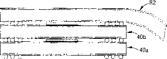
As shown in figure 12, upside-down mounting chip BGA encapsulation body 40b can connect a soft board device (flex-board) 82, to connect other circuit external.As shown in figure 13, upside-down mounting chip BGA encapsulation body 40b also can connect a heat abstractor (heat slug) 84, improves radiating effect.Heat abstractor 84 can be manufactured into the external form (not shown) of a BGA substrate, also is made into metal (copper) fin as Figure 13 or the external form (not shown) of other radiating wings.
As shown in figure 14, the tin ball pad 58b on the upside-down mounting chip BGA encapsulation body 40b can be used for connecting a checkout gear 86, conveniently to carry out circuit test.Checkout gear 86 includes a test probe head (tester head) 88, reaches a plurality of probes (pogo pins) 90 and is located at the test probe head 88 times, can contact with tin ball pad 58b to form to be electrically connected.
The above various subsidiary components of enumerating also can be applied on the upside-down mounting chip BGA encapsulation body via suitable combination to each other.For example the impedance termination coalignment 72 among Fig. 9 can be installed on the upside-down mounting chip BGA encapsulation body 40c of Figure 10, and the heat abstractor 84 of Figure 13 also can be installed on the impedance termination coalignment 72 of Fig. 9.In addition, other upside-down mounting chip BGA encapsulation body 40 and subsidiary components can further be piled up in upside-down mounting chip BGA encapsulation body 40a below among Fig. 9 to Figure 14, be installed to again at last on the printed circuit board (PCB) (not shown), for example a motherboard (mother board) or an auxiliary insert card (daughtercard).For simplicity of illustration, aforementioned upside-down mounting chip BGA encapsulation body 40a, 40b, 40c, the schematic diagram when 40d piles up are not drawn the internal structure of upside-down mounting chip BGA encapsulation body 40a, 40b, 40c, 40d.Be that its internal structure can be a two-ply, four laminates or other multiple-plate structures.
Please refer to Figure 15, Figure 15 is the generalized section of second embodiment of the utility model upside-down mounting chip BGA encapsulation body.Figure 15 shows that one or four laminate upside-down mounting chip BGA encapsulation bodies 92, its outward appearance is identical with two-layer upside-down mounting chip BGA encapsulation body 40, but includes at least one copper conductor layer 94 (being two-layer internal layer copper conductor layer 94 in Figure 15) in the substrate 42 in addition.The copper conductor layer 46 and 48 of substrate 42, internal layer copper conductor layer 94 and circuit pathways 50 are passed through suitable being connected, and can be electrically connected the convex pads 56 and tin ball pad 58,60 of substrate 42.Same, the application of two-ply upside-down mounting chip BGA encapsulation body 40 mentioned above also extends on the upside-down mounting chip BGA encapsulation body 92 or other multiple-plate upside-down mounting chip BGA encapsulation bodies of four laminates.
Please refer to Figure 16, Figure 16 is the schematic diagram that piles up of the 3rd embodiment of the utility model upside-down mounting chip BGA encapsulation body.As shown in figure 16, the upside-down mounting chip BGA encapsulation body 96 of the utility model the 3rd embodiment is made of a substrate 98 and an IC chip 100, and upside-down mounting chip BGA encapsulation body 96 is that with upside-down mounting chip BGA encapsulation body 40 differences chip 100 is fixed on the below of substrate 98.Upside-down mounting chip BGA encapsulation body 96 remaining structure or itself and other element ways of connecting can be according to the combinations that is applied of aforementioned upside-down mounting chip BGA encapsulation body 40.
The substrate 98 of BGA packaging body 96 is very close with substrate 42 both structures of BGA packaging body 40, the both is not provided with a chip lock chamber, and substrate is respectively equipped with two copper conductor layers 102,104 in both sides about in the of 98, and the inside of substrate 98 then is provided with a plurality of circuit pathways (not shown)s and is used for connecting copper conductor layer 102 and copper conductor layer 104.The inside of substrate 98 can be provided with at least one internal layer copper conductor layer (not shown) in addition, is used for being electrically connected circuit pathways, copper conductor layer 102 and copper conductor layer 104.
The surface of copper conductor layer 102,104 covers two green enamelled coatings 106,108 respectively.The green enamelled coating 106 of substrate 98 upsides is provided with a plurality of tin ball pad 110, and the green enamelled coating 108 of substrate 98 downsides then is provided with a plurality of tin ball pad 112 and a plurality of convex pads 114.Convex pads 114 is distributed in the presumptive area (not shown) under the substrate, and 112 of tin ball pad are distributed in outside this presumptive area.
The downside of IC chip 100 is provided with a plurality of joint sheet (not shown)s, and its position is corresponding with the position of substrate 98 upper protruding block weld pads 114.IC chip 100 utilizes a plurality of solder projections or conducting polymer projection 116 to be secured in the downside of substrate 98, and IC chip 100 is electrically connected on the substrate 98.Can fill a bottom sealant (not shown) between IC chip 100 and the substrate 98 in addition, to fill up the space between IC chip 100 and the substrate 98.
The position of the tin ball pad 110 of upside-down mounting chip BGA encapsulation body 96 upsides is corresponding to the tin ball pad 112 of another upside-down mounting chip BGA encapsulation body 96 downsides, and can between tin ball pad 110 and corresponding tin ball pad 112, form a plurality of soldering balls 118, with repeatedly stacking upside-down mounting chip BGA encapsulation body 96.Middle body at substrate 98 upsides can be provided with a plurality of tin ball pad (not shown)s in addition, and these tin ball pad are not connected with other packaging bodies or element, but is used for increasing the radiating effect of substrate 98.
In addition, the tin ball pad 110 of upside-down mounting chip BGA encapsulation body 96 upsides can connect an impedance termination coalignment, an impedance-matching device, a soft board device, a heat abstractor or other welded ball array packaging body (not shown)s via soldering ball 118.Tin ball pad 110 also can directly be electrically connected a checkout gear (not shown), and it includes an at least one probe or a test probe head, to contact with tin ball pad 110.The tin ball pad 112 of upside-down mounting chip BGA encapsulation body 96 downsides also can connect an impedance-matching device or a printed circuit board (PCB) (not shown) via soldering ball 118.Printed circuit board (PCB) can be a motherboard or an auxiliary insert card.
The characteristics of the utility model upside-down mounting chip BGA encapsulation body 40,92,96 are can repeatedly stacking, and can be combined with other subsidiary components.Therefore in high speed memory modules (high speed memorymodule), upside-down mounting chip BGA encapsulation body 40,92,96 provides a kind of encapsulating structure of high packaging density.Because upside-down mounting chip BGA encapsulation body 40,92,96 can significantly reduce area shared on printed circuit board (PCB), and shorten the distance of signal transmission.For system designer, upside-down mounting chip BGA encapsulation body 40,92,96 can be as a kind of hardware platform of high speed, and for the IC designer, 40,92,96 of upside-down mounting chip BGA encapsulation bodies can provide the allowance (timingconstraint margin) of preferable sequential restriction, and can widely apply at high speed storing chip (high speed memory chips) or high speed parallel microprocessor (parallel μ-processors).
Compare with existing upside-down mounting chip BGA encapsulation body 10, but upside-down mounting chip BGA encapsulation body 40,92,96 has the function of repeatedly stacking, can utilize printed circuit board area seldom, multilayer upside-down mounting chip BGA encapsulation body 40,92,96 or other subsidiary components are installed, to improve the packaging density (package density) of distributing board level (board level).Simultaneously on high speed circuit, upside-down mounting chip BGA encapsulation body 40,92,96 modes with mutual correspondence connect, therefore the synchronism (synchronization) of high-frequency signal is not vulnerable to the influence of electron circuit layout on the printed circuit board (PCB) (layout), and can improve the synchronism on the high-frequency signal sequential.