CN218997936U - Charge pump circuit, chip and electronic equipment - Google Patents
Charge pump circuit, chip and electronic equipment Download PDFInfo
- Publication number
- CN218997936U CN218997936U CN202223136509.8U CN202223136509U CN218997936U CN 218997936 U CN218997936 U CN 218997936U CN 202223136509 U CN202223136509 U CN 202223136509U CN 218997936 U CN218997936 U CN 218997936U
- Authority
- CN
- China
- Prior art keywords
- switching device
- module
- capacitor module
- switch
- switch module
- Prior art date
- Legal status (The legal status is an assumption and is not a legal conclusion. Google has not performed a legal analysis and makes no representation as to the accuracy of the status listed.)
- Active
Links
Images


Classifications
-
- Y—GENERAL TAGGING OF NEW TECHNOLOGICAL DEVELOPMENTS; GENERAL TAGGING OF CROSS-SECTIONAL TECHNOLOGIES SPANNING OVER SEVERAL SECTIONS OF THE IPC; TECHNICAL SUBJECTS COVERED BY FORMER USPC CROSS-REFERENCE ART COLLECTIONS [XRACs] AND DIGESTS
- Y02—TECHNOLOGIES OR APPLICATIONS FOR MITIGATION OR ADAPTATION AGAINST CLIMATE CHANGE
- Y02B—CLIMATE CHANGE MITIGATION TECHNOLOGIES RELATED TO BUILDINGS, e.g. HOUSING, HOUSE APPLIANCES OR RELATED END-USER APPLICATIONS
- Y02B70/00—Technologies for an efficient end-user side electric power management and consumption
- Y02B70/10—Technologies improving the efficiency by using switched-mode power supplies [SMPS], i.e. efficient power electronics conversion e.g. power factor correction or reduction of losses in power supplies or efficient standby modes
Landscapes
- Dc-Dc Converters (AREA)
Abstract
The present disclosure provides a charge pump circuit, chip and apparatus, the circuit comprising: a capacitor module and a switch module; the capacitor module comprises an input capacitor module, a conversion capacitor module and an output capacitor module; the switch module comprises a first switch module and a second switch module; the first switch module is connected between the input capacitor module and the conversion capacitor module; the second switch module is connected between the conversion capacitor module and the output capacitor module; when the first switch module and the second switch module are in different switch states, the input capacitor module charges the conversion capacitor and the conversion capacitor module charges the output capacitor module, so that the obtained input voltage of the input capacitor module and the output voltage of the output capacitor module are in a preset ratio; wherein the switch state comprises an on state and/or an off state. Therefore, the preset ratio of the input voltage to the output voltage is different, so that the charge pump circuit can work in a charging working mode corresponding to the different preset ratio.
Description
Technical Field
The present disclosure relates to the field of integrated circuits, and in particular, to a charge pump circuit, a chip, and an electronic device.
Background
In recent years, various portable electronic products have been rapidly developed. As an important component of electronic products, the power supply has the specification requirements of high efficiency, small quiescent current, small volume, low cost and the like. Therefore, the charge pump circuit becomes the preferred power supply for the electronic product.
With the rapid development of the charge chip technology, charge pump charge chips are layered endlessly and have various types, but the charge pump charge chips are generally high in cost and complex in circuit, and more capacitance devices are needed, so that the charge pump charge chips are more in layout occupation area.
Disclosure of Invention
The embodiment of the disclosure discloses a charge pump circuit, a chip and electronic equipment.
According to a first aspect of embodiments of the present disclosure, there is provided a charge pump circuit comprising: a capacitor module and a switch module; the capacitor module comprises an input capacitor module, a conversion capacitor module and an output capacitor module; the switch module comprises a first switch module and a second switch module;
the first switch module is connected between the input capacitor module and the conversion capacitor module; the second switch module is connected between the conversion capacitor module and the output capacitor module;
When the first switch module and the second switch module are in different switch states, the input capacitor module charges the conversion capacitor and the conversion capacitor module charges the output capacitor module, so that the obtained input voltage of the input capacitor module and the output voltage of the output capacitor module are in a preset ratio; wherein the switch state comprises an on state and/or an off state.
In some embodiments, the input capacitor module charges the conversion capacitor module when the first switch module is in an on state and the second switch module is in an off state, and the conversion capacitor module charges the output capacitor module when the first switch module is in an off state and the second switch module is in an on state, so that a ratio of an input voltage of the input capacitor module to an output voltage of the output capacitor module is a first ratio.
In some embodiments, the input capacitance module comprises at least one input capacitance; the conversion capacitor module includes: at least three switching capacitances; at least three of the conversion capacitors are connected in parallel; the output capacitor module comprises at least one output capacitor;
Wherein the voltage of the conversion capacitor is smaller than the voltage of the input capacitor; the voltage of the output capacitor is less than or equal to the voltage of the conversion capacitor.
In some embodiments, the first switch module comprises: at least one first switching device; the second switch module includes: a second switching device, a third switching device, a fourth switching device, a fifth switching device, and a sixth switching device;
the drain electrode of the first switching device is connected with the first end of the input capacitor module, and the source electrode of the first switching device is connected with the first end of the conversion capacitor module;
the drain electrode of the second switching device is connected with the first end of the conversion capacitor module, and the source electrode of the second switching device is connected with the first end of the output capacitor module;
the drain electrode of the third switching device is connected with the first end of the output capacitor module, and the source electrode of the third switching device is connected with the second end of the conversion capacitor module;
the drain electrode of the fourth switching device is connected with the source electrode of the third switching device, and the source electrode of the fourth switching device is connected with the second end of the output capacitor module;
The drain electrode of the fifth switching device is connected with the first end of the output capacitor module, and the source electrode of the fifth switching device is connected with the second end of the conversion capacitor module;
and the drain electrode of the sixth switching device is connected with the source electrode of the fifth switching device, and the source electrode of the sixth switching device is connected with the second end of the output capacitor module.
In some embodiments, the on state of the first switch module is: the first switching device is conducted; the disconnection state of the second switch module is as follows: the second switching device is turned off, the third switching device is turned on, the fourth switching device is turned off, the fifth switching device is turned on, and the six switching device is turned off;
and/or the number of the groups of groups,
the disconnection state of the first switch module is as follows: the first switching device is turned off; the on state of the second switch module is as follows: the second switching device is turned on, the third switching device is turned off, the fourth switching device is turned on, the fifth switching device is turned off, and the six switching devices are turned on.
In some embodiments, the switched capacitor module includes: the first conversion capacitor module, the second conversion capacitor module and the third conversion capacitor module; switch module still includes: a third switch module and a fourth switch module; the third switch module is connected between the first end of the first conversion capacitor module and the first end of the second conversion capacitor module, and the fourth switch module is connected between the first end of the second conversion capacitor module and the first end of the third conversion capacitor module;
When the first switch module and the fourth switch module are in a conducting state, and the second switch module and the third switch module are in a disconnecting state, the input capacitor module charges the first switch capacitor module and/or the second switch capacitor module charges the third switch capacitor module, and when the first switch module and the fourth switch module are in a disconnecting state, and the second switch module and the third switch module are in a conducting state, the first switch capacitor module charges the second switch capacitor module and/or the third switch capacitor module charges the output capacitor module, so that the input voltage of the input capacitor module and the output voltage of the output capacitor module are in a second ratio.
In some embodiments, the first switch module comprises: at least one first switching device; the second switch module includes: a second switching device, a third switching device, a fourth switching device, a fifth switching device, and a sixth switching device; the third switch module includes: at least one seventh switching device; a fourth switch module comprising: at least one eighth switching device;
The drain electrode of the first switching device is connected with the first end of the input capacitor module, and the source electrode of the first switching device is connected with the first end of the first conversion capacitor module;
the drain electrode of the second switching device is connected with the first end of the third conversion capacitor module, and the source electrode of the second switching device is connected with the first end of the output capacitor;
the drain electrode of the third switching device is connected with the first end of the output capacitor module, and the source electrode of the third switching device is connected with the first conversion capacitor module and the second end of the third conversion capacitor module;
the drain electrode of the fourth switching device is connected with the source electrode of the third switching device, and the source electrode of the fourth switching device is connected with the second end of the output capacitor module;
the drain electrode of the fifth switching device is connected with the first end of the output capacitor module, and the source electrode of the fifth switching device is connected with the second end of the second conversion capacitor module;
the drain electrode of the sixth switching device is connected with the source electrode of the fifth switching device, and the source electrode of the sixth switching device is connected with the second end of the output capacitor module;
the drain electrode of the seventh switching device is connected with the source electrode of the first switching device, and the source electrode of the seventh switching device is connected with the first end of the second conversion capacitor module;
The drain electrode of the eighth switching device is connected with the source electrode of the seventh switching device, and the source electrode of the eighth switching device is connected with the first end of the third conversion capacitor module.
In some embodiments, the on state of the first switch module and the fourth switch module includes: the first switching device and the eighth switching device are turned on; the disconnection state of the second switch module and the third switch module comprises: the second switching device is turned off, the third switching device is turned on, the fourth switching device is turned off, the fifth switching device is turned off, the sixth switching device is turned on, and the seventh switching device is turned off;
or,
the disconnection state of the first switch module and the fourth switch module comprises: the first switching device and the eighth switching device are turned off; the conducting state of the second switch module and the third switch module comprises: the second switching device is turned on, the third switching device is turned off, the fourth switching device is turned on, the fifth switching device is turned on, the sixth switching device is turned off, and the seventh switching device is turned on.
According to a second aspect of embodiments of the present disclosure, there is provided a chip comprising a charge pump circuit as described in any of the embodiments of the present disclosure.
According to a third aspect of embodiments of the present disclosure, there is provided an electronic device comprising a charge pump circuit as described in any of the embodiments of the present disclosure or a chip as described in any of the embodiments of the present disclosure.
The technical scheme provided by the embodiment of the disclosure can comprise the following beneficial effects:
in an embodiment of the present disclosure, there is provided a charge pump circuit including: a capacitor module and a switch module; the capacitor module comprises an input capacitor module, a conversion capacitor module and an output capacitor module; the switch module comprises a first switch module and a second switch module; the first switch module is connected between the input capacitor module and the conversion capacitor module; the second switch module is connected between the conversion capacitor module and the output capacitor module; when the first switch module and the second switch module are in different switch states, the input capacitor module charges the conversion capacitor and the conversion capacitor module charges the output capacitor module, so that the obtained output voltage of the input capacitor module and the output voltage of the input capacitor module are in a preset ratio; wherein the switch state comprises an on state and/or an off state.
In this way, in the charge pump circuit, when the first switch module and the second switch module are in different switch states, the input capacitor module charges the capacitor module and the conversion capacitor module charges the output capacitor module, so that the obtained output voltage of the input capacitor module and the output voltage of the input capacitor module are in a preset ratio, and the conversion of the input voltage of the input capacitor module to the required voltage can be realized and the output can be realized; the input voltage of the input capacitor module and the voltage of the conversion capacitor module can be different, meaning that the preset ratio can be different, and the charge pump circuit can work in a charging working mode corresponding to the different preset ratio. By changing the input voltage of the input capacitor module, for example, reducing the input voltage of the input capacitor module, the input capacitor number of the input capacitor module can be reduced, so that the cost is reduced, and the layout occupation area of the charge pump charging chip can be reduced due to the reduction of the input capacitor number.
It is to be understood that both the foregoing general description and the following detailed description are exemplary and explanatory only and are not restrictive of the disclosure.
Drawings
The accompanying drawings, which are incorporated in and constitute a part of this specification, illustrate embodiments consistent with the disclosure and together with the description, serve to explain the principles of the disclosure.
Fig. 1 is a schematic structural diagram of an electronic device according to an embodiment of the present disclosure;
fig. 2 is a schematic diagram of a charge pump circuit according to an embodiment of the disclosure;
fig. 3 is a schematic diagram of a switch state switching structure of a charge pump circuit according to an embodiment of the disclosure;
fig. 4 is a schematic diagram of a charge pump circuit according to an embodiment of the disclosure;
fig. 5 is a schematic diagram of a charge pump circuit according to an embodiment of the disclosure;
fig. 6 is a schematic diagram of a charge pump circuit according to an embodiment of the disclosure;
fig. 7 is a schematic diagram of a charge pump circuit according to an embodiment of the disclosure;
fig. 8 is a schematic structural diagram of an electronic device according to an embodiment of the disclosure;
fig. 9 is a schematic diagram of a charge pump circuit according to an embodiment of the disclosure;
fig. 10 is a schematic structural diagram of an electronic device according to an embodiment of the present disclosure;
FIG. 11A is a schematic diagram of a chip according to an embodiment of the disclosure;
FIG. 11B is a schematic diagram of a chip according to an embodiment of the disclosure;
Fig. 12 is a schematic structural diagram of an electronic device according to an embodiment of the present disclosure.
Detailed Description
Reference will now be made in detail to exemplary embodiments, examples of which are illustrated in the accompanying drawings. When the following description refers to the accompanying drawings, the same numbers in different drawings refer to the same or similar elements, unless otherwise indicated. The implementations described in the following exemplary examples are not representative of all implementations consistent with the present disclosure. Rather, they are merely examples of apparatus consistent with some aspects of the disclosure as detailed in the accompanying claims.
The terminology used in the embodiments of the disclosure is for the purpose of describing particular embodiments only and is not intended to be limiting of the embodiments of the disclosure. As used in this disclosure and the appended claims, the singular forms "a," "an," and "the" are intended to include the plural forms as well, unless the context clearly indicates otherwise. It should also be understood that the term "and/or" as used herein refers to and encompasses any or all possible combinations of one or more of the associated listed items.
It should be understood that although the terms first, second, third, etc. may be used in embodiments of the present disclosure to describe various information, these information should not be limited to these terms. These terms are only used to distinguish one type of information from another. For example, the first information may also be referred to as second information, and similarly, the second information may also be referred to as first information, without departing from the scope of embodiments of the present disclosure. The word "if" as used herein may be interpreted as "at … …" or "at … …" or "responsive to a determination", depending on the context.
In the related art, the electronic device can realize 40W power charging by using a single 2:1 charge pump charging chip; as shown in fig. 1, the parallel charging of two 2:1 charge pump charging chips can achieve 67W power charging, but the two 2:1 charge pump charging chips have more components and higher cost.
As shown in fig. 2, an embodiment of the present disclosure provides a charge pump circuit 110, including: a capacitor module and a switch module; the capacitor module comprises an input capacitor module 111, a conversion capacitor module 112 and an output capacitor module 113; the switch module comprises a first switch module 121 and a second switch module 122;
the first switch module 121 is connected between the input capacitor module 111 and the conversion capacitor module 112; the second switch module 122 is connected between the conversion capacitor module 112 and the output capacitor module 113;
when the first switch module 121 and the second switch module 122 are in different switch states, the input capacitor module 111 charges the conversion capacitor 112 and the conversion capacitor module 112 charges the output capacitor module 113, so that the obtained input voltage of the input capacitor module 111 and the output voltage of the output capacitor module 113 are in a predetermined ratio; wherein the switch state comprises an on state and/or an off state.
Here, the capacitor module comprises at least one capacitor; the capacitor module is used for charging and/or discharging in two switch states; the capacitor modules include an input capacitor module 111, a conversion capacitor module 112, and an output capacitor module 113.
Here, the input capacitor module 111 is used to charge the conversion capacitor module 112.
Here, the switched capacitor module 112 is used to charge the output capacitor module 113.
Here, the output capacitor module 113 is used for outputting a voltage to charge the electronic device.
Here, the voltage magnitude of the capacitor is positively correlated with the number of capacitors. Illustratively, the greater the number of input capacitances, the greater the voltage of the input capacitances.
Here, the switching module includes at least one switching device; the charge pump circuit is used for changing the switching state of the charge pump circuit so as to control the capacitor module to charge or discharge; the switch modules include a first switch module 121 and a second switch module 122.
Here, the switching device may be a common single control switch, a transistor, a MOS (Metal Oxide Semiconductor Field Effect Transistor, metal oxide semiconductor type field effect transistor) transistor, an IGBT (Insulated Gate Bipolar Transistor ) transistor, or the like.
In some embodiments, the MOS transistors are divided into P-type MOS transistors and N-type MOS transistors, i.e., PMOS transistors and NMOS transistors. The MOS tube comprises three pins: g-electrode (gate) -gate; source electrode; d pole (drain) -drain.
Here, the predetermined ratio may be any ratio. Illustratively, the predetermined ratio may be 4:1, 4:2, 2:1, 1:1, or the like.
In one embodiment, the charging mode of operation in which the charge pump circuit is configured to operate is determined based on the magnitude of the predetermined ratio. Illustratively, the predetermined ratio is 1:1, and the charge pump circuit is configured to operate in a 1:1 charge mode of operation.
Here, the switching state includes an on state and/or an off state.
In some embodiments, the charge pump circuit further comprises a control module connected to the switch module, and the control module is used for controlling the on-off state of the switch module. Illustratively, the control module sends a first signal to the switch module, the first signal being for controlling the switch module to enter a conductive state; or the control module sends a second signal to the switch module, wherein the second signal is used for controlling the switch module to enter the off state.
Here, the first signal and/or the second signal may be a clock signal, a pulse signal, or any one of control signals.
In one embodiment, as shown in fig. 2, the first switch module 121 is connected between the input capacitor module 111 and the conversion capacitor module 112; the second switch module 122 is connected between the conversion capacitor module 112 and the output capacitor module 113, and includes:
the first end of the input capacitor module 111 is connected to the first end of the first switch module 121, the second end of the first switch module 121 is connected to the first end of the second switch module 122, and the second end of the second switch module 122 is connected to the first end of the output capacitor module 113.
In this way, in the charge pump circuit, when the first switch module and the second switch module are in different switch states, the input capacitor module charges the capacitor module and the conversion capacitor module charges the output capacitor module, so that the obtained output voltage of the input capacitor module and the output voltage of the input capacitor module are in a preset ratio, and the conversion of the input voltage of the input capacitor module to the required voltage and the output can be realized; the input voltage of the input capacitor module and the voltage of the conversion capacitor module can be different, meaning that the preset ratio can be different, and the charge pump circuit can work in a charging working mode corresponding to the different preset ratio. By changing the input voltage of the input capacitor module, for example, reducing the input voltage of the input capacitor module, the input capacitor number of the input capacitor module can be reduced, so that the cost is reduced, and the layout occupation area of the charge pump charging chip can be reduced due to the reduction of the input capacitor number.
In one embodiment, as shown in fig. 3, the input capacitor module 210 charges the conversion capacitor module 230 when the first switch module 220 is in the on state and the second switch module 240 is in the off state, and the conversion capacitor module 230 charges the output capacitor module 250 when the first switch module 220 is in the off state and the second switch module 240 is in the on state, so that the ratio of the input voltage of the input capacitor module 210 to the output voltage of the output capacitor module 250 is a first ratio.
Here, the first ratio is 2:1. The charge pump circuit is configured to operate in a 2:1 charge mode of operation.
In some embodiments, the input capacitance module comprises at least one input capacitance; the conversion capacitor module includes: at least three switching capacitances; at least three of the conversion capacitors are connected in parallel; the output capacitor module comprises at least one output capacitor;
wherein the voltage of the conversion capacitor is smaller than the input voltage of the input capacitor; the voltage of the output capacitor is smaller than or equal to the output voltage of the conversion capacitor.
In one embodiment, as shown in FIG. 4, a schematic diagram of a charge pump circuit in a 2:1 charge mode of operation is provided. The capacitor module comprises five capacitors, and the Input capacitor module comprises an Input capacitor Vin (Voltage Input end before Voltage stabilization); the conversion capacitor module comprises three conversion capacitors which are C1, C2 and C3 respectively, and the three conversion capacitors of C1, C2 and C3 are connected in parallel; the Output capacitor module includes an Output capacitor Vout (Voltage Output terminal after Voltage stabilization).
The voltages of the three conversion capacitors are 5V, the input voltage of the input capacitor Vin is 10V, and the voltages of the conversion capacitors are smaller than those of the input capacitor; the output voltage of the output capacitor Vout is 5V, and the output voltage of the output capacitor is equal to the voltage of the conversion capacitor. The ratio of the input voltage of the input capacitor Vin to the output voltage of the output capacitor is 2:1.
In some embodiments, the first switch module comprises: at least one first switching device; the second switch module includes: a second switching device, a third switching device, a fourth switching device, a fifth switching device, and a sixth switching device;
the drain electrode of the first switching device is connected with the first end of the input capacitor module, and the source electrode of the first switching device is connected with the first end of the conversion capacitor module;
the drain electrode of the second switching device is connected with the first end of the conversion capacitor module, and the source electrode of the second switching device is connected with the first end of the output capacitor module;
the drain electrode of the third switching device is connected with the first end of the output capacitor module, and the source electrode of the third switching device is connected with the second end of the conversion capacitor module;
The drain electrode of the fourth switching device is connected with the source electrode of the third switching device, and the source electrode of the fourth switching device is connected with the second end of the output capacitor module;
the drain electrode of the fifth switching device is connected with the first end of the output capacitor module, and the source electrode of the fifth switching device is connected with the second end of the conversion capacitor module;
and the drain electrode of the sixth switching device is connected with the source electrode of the fifth switching device, and the source electrode of the sixth switching device is connected with the second end of the output capacitor module.
In some embodiments, the first end of the capacitor module is a positive electrode of a capacitor in the capacitor module, and the second end of the capacitor module is a negative electrode of the capacitor in the capacitor module; or the first end of the capacitor module is the negative electrode of the capacitor in the capacitor module, and the second end of the capacitor module is the positive electrode of the capacitor in the capacitor module correspondingly.
In some embodiments, the on state of the first switch module is: the first switching device is conducted; the disconnection state of the second switch module is as follows: the second switching device is turned off, the third switching device is turned on, the fourth switching device is turned off, the fifth switching device is turned on, and the six switching device is turned off;
And/or the number of the groups of groups,
the disconnection state of the first switch module is as follows: the first switching device is turned off; the on state of the second switch module is as follows: the second switching device is turned on, the third switching device is turned off, the fourth switching device is turned on, the fifth switching device is turned off, and the six switching devices are turned on.
In one embodiment, as shown in fig. 4, the switch modules include a first switch module and a second switch module. The first switch module includes a first switching device Q1, and the second switch module includes: the second switching device Q4, the third switching device Q5, the fourth switching device Q6, the fifth switching device Q8 and the sixth switching device Q7 are in a normally-on state, the third switching device Q5 and the fifth switching device Q8 are connected in parallel, and the fourth switching device Q6 and the sixth switching device Q7 are connected in parallel. The input capacitor module comprises an input capacitor Vin; the conversion capacitor module comprises three conversion capacitors which are C1, C2 and C3 respectively, and the three conversion capacitors of C1, C2 and C3 are connected in parallel; the output capacitor module comprises an output capacitor Vout.
The first end of the input capacitor module is the positive electrode of the input capacitor in the input capacitor module, and the second end of the input capacitor module is the negative electrode of the input capacitor in the input capacitor module; the first end of the conversion capacitor module is the positive electrode of the conversion capacitor in the conversion capacitor module, and the second end is the negative electrode of the conversion capacitor in the conversion capacitor module; the first end of the output capacitor module is the positive electrode of the output capacitor in the output capacitor module, and the second end is the negative electrode of the output capacitor in the output capacitor module.
The drain electrode of Q1 is connected with the first end of Vin, and the source electrode of Q1 is connected with the first end of C1;
the drain electrode of the Q4 is connected with the first end of the C3, and the source electrode of the Q4 is connected with the first end of the Vout;
q5 is connected with the first end of Vout, and the source electrode of Q5 is connected with the second ends of C1 and C3;
the drain electrode of the Q6 is connected with the source electrode of the Q5, and the source electrode of the Q6 is connected with the second end of the Vout;
the drain electrode of the Q8 is connected with the first end of Vout, and the source electrode of the Q8 is connected with the second end of C2;
the drain of Q7 is connected to the source of Q8, and the source of Q7 is connected to the second terminal of C2.
The on state of the first switch module in the charging working mode is as follows: the first switching device Q1 is turned on; the disconnection state of the second switch module is as follows: the second switching device Q4 is turned off, the third switching device Q5 is turned on, the fourth switching device Q6 is turned off, the fifth switching device Q8 is turned on, and the sixth switching device Q7 is turned off; as shown in fig. 5, the input capacitor Vin charges the conversion capacitors C1, C2 and C3 simultaneously.
The disconnection state of the first switch module is as follows: the first switching device Q1 is turned off; the second switch module has a conducting state that: the second switching device Q4 is on, the third switching device Q5 is off, the fourth switching device Q6 is on, the fifth switching device Q8 is off, and the sixth switching device Q7 is on; as shown in fig. 6, the output capacitor Vout is charged simultaneously by the conversion capacitors C1, C2 and C3.
In one embodiment, as shown in fig. 7, the first switching device Q1 and the second switching device Q4 may be connected by a wire.
In one embodiment, as shown in fig. 8, the present disclosure may apply the charge pump circuit of a 4:1 charge pump charging chip to a 2:1 charge mode of operation.
In this way, the embodiment of the disclosure can realize that the charge pump circuit of the 4:1 charge pump charging chip is applied to the 2:1 charging working mode. On the one hand, compared with the charging by using two 2:1 charge pump charging chips, the charging by using the single 4:1 charge pump charging chip in the embodiment of the disclosure can realize equal power charging, and the cost is reduced. On the other hand, compared with the 4:1 charge pump charging chip, the output voltage is reduced to one fourth of the input voltage in the 4:1 charge operation mode, for example, the input voltage is reduced to one fourth of 20V, namely, the output voltage is 5V; in the embodiment of the disclosure, the charge pump circuit using the 4:1 charge pump charging chip is applied to a 2:1 charging working mode, the output voltage is reduced to one half of the input voltage, for example, the input voltage is reduced to one half, namely, the output voltage is 5V, the input voltage can be reduced, the number of input capacitors can be reduced, the layout occupation area of the 4:1 charge pump charging chip can be reduced due to the reduction of the number of capacitors, and the cost and the resource can be reduced.
In some embodiments, the fourth switching device, the sixth switching device, and/or the output capacitance mode ground.
In one embodiment, as shown in fig. 4, when the first switch module is in an on state and the second switch module is in an off state, one end of the output capacitor Vout in the output capacitor module is grounded. When the first switch module is in an off state and the second switch module is in an on state, the fourth switch device Q6 and the sixth switch device Q7 are grounded.
Therefore, the safety coefficient of the charge pump circuit can be improved through grounding, electrostatic damage is prevented, and the balance of ground potential and the normal operation of the charge pump charging chip and the electronic equipment where the charge pump charging chip is located are ensured.
In some embodiments, the switched capacitor module includes: the first conversion capacitor module, the second conversion capacitor module and the third conversion capacitor module; the switch module includes the switch module, still includes: a third switch module and a fourth switch module; the third switch module is connected between the first end of the first conversion capacitor module and the first end of the second conversion capacitor module, and the fourth switch module is connected between the first end of the second conversion capacitor module and the first end of the third conversion capacitor module;
When the first switch module and the fourth switch module are in a conducting state, and the second switch module and the third switch module are in a disconnecting state, the input capacitor module charges the first switch capacitor module and/or the second switch capacitor module charges the third switch capacitor module, and when the first switch module and the fourth switch module are in a disconnecting state, and the second switch module and the third switch module are in a conducting state, the first switch capacitor module charges the second switch capacitor module and/or the third switch capacitor module charges the output capacitor module, so that the input voltage of the input capacitor module and the output voltage of the output capacitor module are in a second ratio.
Here, the second ratio is 4:1. The charge pump circuit is configured to operate in a 4:1 charge mode of operation.
In one embodiment, as shown in FIG. 9, a schematic diagram of a charge pump circuit in a 4:1 charge mode of operation is provided. The conversion capacitor module comprises first to third conversion capacitor modules, the first conversion capacitor module comprises a first conversion capacitor C1, the second conversion capacitor module comprises a second conversion capacitor C2, and the third conversion capacitor module comprises a third conversion capacitor C3. The input capacitor module comprises an input capacitor Vin; the output capacitor module comprises an output capacitor Vout. The input voltage of the input capacitor Vin is 20V, the voltage of the first conversion capacitor C1 is 15V, the voltage of the second conversion capacitor C2 is 10V, the voltage of the third conversion capacitor C3 is 5V, and the output voltage of the output capacitor Vout is 5V; the ratio of the input voltage of the input capacitor Vin to the output voltage of the output capacitor Vout is 4:1.
The first end of the conversion capacitor module is the positive electrode of the conversion capacitor in the conversion capacitor module, and the second end of the conversion capacitor module is the negative electrode of the conversion capacitor in the conversion capacitor module. The third switch module is connected between the first end of C1 and the first end of C2; the fourth switch module is connected between the first end of C2 and the first end of C3.
In some embodiments, the first switch module comprises: at least one first switching device; the second switch module includes: a second switching device, a third switching device, a fourth switching device, a fifth switching device, and a sixth switching device; the third switch module includes: at least one seventh switching device; a fourth switch module comprising: at least one eighth switching device;
the drain electrode of the first switching device is connected with the first end of the input capacitor module, and the source electrode of the first switching device is connected with the first end of the first conversion capacitor module;
the drain electrode of the second switching device is connected with the first end of the third conversion capacitor module, and the source electrode of the second switching device is connected with the first end of the output capacitor;
the drain electrode of the third switching device is connected with the first end of the output capacitor module, and the source electrode of the third switching device is connected with the first conversion capacitor module and the second end of the third conversion capacitor module;
The drain electrode of the fourth switching device is connected with the source electrode of the third switching device, and the source electrode of the fourth switching device is connected with the second end of the output capacitor module;
the drain electrode of the fifth switching device is connected with the first end of the output capacitor module, and the source electrode of the fifth switching device is connected with the second end of the second conversion capacitor module;
the drain electrode of the sixth switching device is connected with the source electrode of the fifth switching device, and the source electrode of the sixth switching device is connected with the second end of the output capacitor module;
the drain electrode of the seventh switching device is connected with the source electrode of the first switching device, and the source electrode of the seventh switching device is connected with the first end of the second conversion capacitor module;
the drain electrode of the eighth switching device is connected with the source electrode of the seventh switching device, and the source electrode of the eighth switching device is connected with the first end of the third conversion capacitor module.
In some embodiments, the first end of the capacitor module is a positive electrode of a capacitor in the capacitor module, and the second end of the capacitor module is a negative electrode of the capacitor in the capacitor module; or the first end of the capacitor module is the negative electrode of the capacitor in the capacitor module, and the second end of the capacitor module is the positive electrode of the capacitor in the capacitor module correspondingly.
In some embodiments, the on state of the first switch module and the fourth switch module includes: the first switching device and the eighth switching device are turned on; the disconnection state of the second switch module and the third switch module comprises: the second switching device is turned off, the third switching device is turned on, the fourth switching device is turned off, the fifth switching device is turned off, the sixth switching device is turned on, and the seventh switching device is turned off;
or,
the disconnection state of the first switch module and the fourth switch module comprises: the first switching device and the eighth switching device are turned off; the conducting state of the second switch module and the third switch module comprises: the second switching device is turned on, the third switching device is turned off, the fourth switching device is turned on, the fifth switching device is turned on, the sixth switching device is turned off, and the seventh switching device is turned on.
In one embodiment, as shown in fig. 9, the conversion capacitor module includes first to third conversion capacitor modules, the first conversion capacitor module includes a first conversion capacitor C1, the second conversion capacitor module includes a second conversion capacitor C2, and the third conversion capacitor module includes a third conversion capacitor C3. The input capacitor module comprises an input capacitor Vin; the output capacitor module comprises an output capacitor Vout.
The switch module comprises a first switch module and a second switch module. The first switch module includes a first switching device Q1, and the second switch module includes: a second switching device Q4, a third switching device Q5, a fourth switching device Q6, a fifth switching device Q8, and a sixth switching device Q7; the third switch module comprises a seventh switch device Q2; the fourth switch module comprises an eighth switch device Q3; the switching devices Q1 to Q8 are NMOS transistors.
The first end of the input capacitor module is the positive electrode of the input capacitor in the input capacitor module, and the second end of the input capacitor module is the negative electrode of the input capacitor in the input capacitor module; the first end of the conversion capacitor module is the positive electrode of the conversion capacitor in the conversion capacitor module, and the second end is the negative electrode of the conversion capacitor in the conversion capacitor module; the first end of the output capacitor module is the positive electrode of the output capacitor in the output capacitor module, and the second end is the negative electrode of the output capacitor in the output capacitor module.
The drain electrode of Q1 is connected with the first end of Vin, and the source electrode of Q1 is connected with the first end of C1;
the drain electrode of the Q4 is connected with the first end of the C3, and the source electrode of the Q4 is connected with the first end of the Vout;
the drain electrode of the Q5 is connected with the first end of Vout, and the source electrode of the Q5 is connected with the second ends of C1 and C3;
The drain electrode of the Q6 is connected with the source electrode of the Q5, and the source electrode of the Q6 is connected with the second end of the Vout;
the drain electrode of the Q8 is connected with the first end of the Vout, and the source electrode of the Q8 is connected with the second end of the second conversion capacitor module;
the drain electrode of the Q7 is connected with the source electrode of the Q8, and the source electrode of the Q7 is connected with the second end of the Vout;
the drain electrode of the Q2 is connected with the source electrode of the Q1, and the source electrode of the Q2 is connected with the first end of the C2;
the drain of Q3 is connected to the source of Q2, and the source of Q3 is connected to the first end of C3.
The on state of the first switch module is as follows: the first switching device Q1 is turned on; the fourth switch module has a conducting state that: the eighth switching device Q3 is turned on; the disconnection state of the second switch module is as follows: the second switching device Q4 is turned off, the third switching device Q5 is turned on, the fourth switching device Q6 is turned off, the fifth switching device Q8 is turned off, and the sixth switching device Q7 is turned on; the disconnection state of the third switch module is as follows: the seventh switching device Q2 is turned off.
The disconnection state of the first switch module is as follows: the first switching device Q1 is turned off; the disconnection state of the fourth switch module is as follows: the eighth switching device Q3 is turned off; the second switch module has a conducting state that: the second switching device Q4 is on, the third switching device Q5 is off, the fourth switching device Q6 is on, the fifth switching device Q8 is on, and the sixth switching device Q7 is off; the conducting state of the third switch module is as follows: the seventh switching device Q2 is turned on.
The 4:1 charging working mode of the charge pump circuit comprises four time sequences, wherein the first time sequence is that the first switch module and the fourth switch module are in a conducting state, the second switch module and the third switch module are in a disconnecting state, and at the moment, the input capacitor Vin charges C1; the second time sequence is that the first switch module and the fourth switch module are in an off state, the second switch module and the third switch module are in an on state, and C1 charges C2 at the moment; the third time sequence is that the first switch module and the fourth switch module are in a conducting state, the second switch module and the third switch module are in a disconnecting state, and C2 charges C3 at the moment; the fourth time sequence is that the first switch module and the fourth switch module are in an off state, the second switch module and the third switch module are in an on state, and at the moment, the C3 charges the output capacitor Vout. Thus, in the 4:1 charging mode of operation, the charge pump circuit may reduce the output voltage to one-fourth of the input voltage. In some embodiments, the fourth switching device, the sixth switching device, and/or the output capacitance mode ground.
In one embodiment, as shown in fig. 9, when the first switch module and the fourth switch module are in the on state and the second switch module and the third switch module are in the off state, the sixth switch device Q7 and the second terminal of the output capacitor Vout in the output capacitor module are grounded. When the first switch module and the fourth switch module are in an off state and the second switch module and the third switch module are in an on state, the fourth switch device Q6 and the second end of the output capacitor Vout in the output capacitor module are grounded.
In one embodiment, as shown in fig. 10, the present disclosure may still enable the charge pump circuit of a 4:1 charge pump charging chip to operate in a 4:1 charge mode of operation.
In this way, the charge pump circuit of the 4:1 charge pump charging chip can be realized according to the requirements, and the charge pump circuit works in a 2:1 charging working mode or works in a 4:1 charging working mode; and for charging by using two 2:1 charge pump charging chips, the embodiment of the disclosure can realize equal power charging by using a single 4:1 charge pump charging chip for charging, and reduce cost.
Embodiments of the present disclosure provide a chip comprising a charge pump circuit of any one of the embodiments of the present disclosure.
In some embodiments, as shown in FIG. 11A, 4 in a 4:1 charging mode of operation is provided; 1 Charge pump Charge chips 910 in 4:1 charge mode, 6 22uF/25V and 8 22uF/16V high voltage capacitors are required for the 4:1 charge pump Charge chips 910.
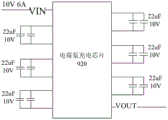
In some embodiments, as shown in fig. 11B, a 4:1 charge pump charging chip 920 in a 2:1 charging mode is provided, and in the 2:1 charging mode, the 4:1 charge pump charging chip 920 does not need to use high voltage power to reduce the cost, and the number of capacitors can be reduced to further reduce the cost, only 8 22uF/10V capacitors are needed, so that the layout occupation area of the 4:1 charge pump charging chip 920 is reduced.
As shown in fig. 12, in an embodiment of the present disclosure, an electronic device 300 is provided, which includes a charge pump circuit according to any of the embodiments of the present disclosure or a chip 310 according to any of the embodiments of the present disclosure.
In one embodiment, as shown in fig. 8, an electronic device includes: the electronic equipment operates in a 4:1 charging working mode, and the ratio of the input voltage of the input capacitor to the output voltage of the output capacitor is 4:1.
In one embodiment, as shown in fig. 10, an electronic device includes: the electronic equipment operates in a 2:1 charging working mode, and the ratio of the input voltage of the input capacitor to the output voltage of the output capacitor is 2:1.
Other embodiments of the disclosure will be apparent to those skilled in the art from consideration of the specification and practice of the disclosure disclosed herein. This disclosure is intended to cover any adaptations, uses, or adaptations of the disclosure following the general principles of the disclosure and including such departures from the present disclosure as come within known or customary practice within the art to which the disclosure pertains. It is intended that the specification and examples be considered as exemplary only, with a true scope and spirit of the disclosure being indicated by the following claims.
It is to be understood that the present disclosure is not limited to the precise arrangements and instrumentalities shown in the drawings, and that various modifications and changes may be effected without departing from the scope thereof. The scope of the present disclosure is limited only by the appended claims.
Claims (10)
1. A charge pump circuit, comprising: a capacitor module and a switch module; the capacitor module comprises an input capacitor module, a conversion capacitor module and an output capacitor module; the switch module comprises a first switch module and a second switch module;
the first switch module is connected between the input capacitor module and the conversion capacitor module; the second switch module is connected between the conversion capacitor module and the output capacitor module;
when the first switch module and the second switch module are in different switch states, the input capacitor module charges the conversion capacitor and the conversion capacitor module charges the output capacitor module, so that the obtained input voltage of the input capacitor module and the output voltage of the output capacitor module are in a preset ratio; wherein the switch state comprises an on state and/or an off state.
2. The circuit of claim 1, wherein the circuit comprises a plurality of capacitors,
when the first switch module is in a conducting state and the second switch module is in a disconnecting state, the input capacitor module charges the conversion capacitor module, and when the first switch module is in a disconnecting state and the second switch module is in a conducting state, the conversion capacitor module charges the output capacitor module, so that the ratio of the input voltage of the input capacitor module to the output voltage of the output capacitor module is a first ratio.
3. The circuit of claim 2, wherein the circuit further comprises a logic circuit,
the input capacitor module comprises at least one input capacitor; the conversion capacitor module includes: at least three switching capacitances; at least three of the conversion capacitors are connected in parallel; the output capacitor module comprises at least one output capacitor;
wherein the voltage of the conversion capacitor is smaller than the voltage of the input capacitor; the voltage of the output capacitor is less than or equal to the voltage of the conversion capacitor.
4. The circuit of claim 3, wherein the circuit comprises a plurality of transistors,
the first switch module includes: at least one first switching device; the second switch module includes: a second switching device, a third switching device, a fourth switching device, a fifth switching device, and a sixth switching device;
The drain electrode of the first switching device is connected with the first end of the input capacitor module, and the source electrode of the first switching device is connected with the first end of the conversion capacitor module;
the drain electrode of the second switching device is connected with the first end of the conversion capacitor module, and the source electrode of the second switching device is connected with the first end of the output capacitor module;
the drain electrode of the third switching device is connected with the first end of the output capacitor module, and the source electrode of the third switching device is connected with the second end of the conversion capacitor module;
the drain electrode of the fourth switching device is connected with the source electrode of the third switching device, and the source electrode of the fourth switching device is connected with the second end of the output capacitor module;
the drain electrode of the fifth switching device is connected with the first end of the output capacitor module, and the source electrode of the fifth switching device is connected with the second end of the conversion capacitor module;
and the drain electrode of the sixth switching device is connected with the source electrode of the fifth switching device, and the source electrode of the sixth switching device is connected with the second end of the output capacitor module.
5. The circuit of claim 4, wherein the circuit further comprises a logic circuit,
The on state of the first switch module is as follows: the first switching device is conducted; the disconnection state of the second switch module is as follows: the second switching device is turned off, the third switching device is turned on, the fourth switching device is turned off, the fifth switching device is turned on, and the six switching device is turned off;
and/or the number of the groups of groups,
the disconnection state of the first switch module is as follows: the first switching device is turned off; the on state of the second switch module is as follows: the second switching device is turned on, the third switching device is turned off, the fourth switching device is turned on, the fifth switching device is turned off, and the six switching devices are turned on.
6. The circuit of claim 1, wherein the circuit comprises a plurality of capacitors,
the conversion capacitor module includes: the first conversion capacitor module, the second conversion capacitor module and the third conversion capacitor module; switch module still includes: a third switch module and a fourth switch module; the third switch module is connected between the first end of the first conversion capacitor module and the second end of the second conversion capacitor module, and the fourth switch module is connected between the first end of the second conversion capacitor module and the first end of the third conversion capacitor module;
When the first switch module and the fourth switch module are in a conducting state, and the second switch module and the third switch module are in a disconnecting state, the input capacitor module charges the first switch capacitor module and/or the second switch capacitor module charges the third switch capacitor module, and when the first switch module and the fourth switch module are in a disconnecting state, and the second switch module and the third switch module are in a conducting state, the first switch capacitor module charges the second switch capacitor module and/or the third switch capacitor module charges the output capacitor module, so that the input voltage of the input capacitor module and the output voltage of the output capacitor module are in a second ratio.
7. The circuit of claim 6, wherein the first switch module comprises: at least one first switching device; the second switch module includes: a second switching device, a third switching device, a fourth switching device, a fifth switching device, and a sixth switching device; the third switch module includes: at least one seventh switching device; a fourth switch module comprising: at least one eighth switching device;
The drain electrode of the first switching device is connected with the first end of the input capacitor module, and the source electrode of the first switching device is connected with the first end of the first conversion capacitor module;
the drain electrode of the second switching device is connected with the first end of the third conversion capacitor module, and the source electrode of the second switching device is connected with the first end of the output capacitor;
the drain electrode of the third switching device is connected with the first end of the output capacitor module, and the source electrode of the third switching device is connected with the first conversion capacitor module and the second end of the third conversion capacitor module;
the drain electrode of the fourth switching device is connected with the source electrode of the third switching device, and the source electrode of the fourth switching device is connected with the second end of the output capacitor module;
the drain electrode of the fifth switching device is connected with the first end of the output capacitor module, and the source electrode of the fifth switching device is connected with the second end of the second conversion capacitor module;
the drain electrode of the sixth switching device is connected with the source electrode of the fifth switching device, and the source electrode of the sixth switching device is connected with the second end of the output capacitor module;
the drain electrode of the seventh switching device is connected with the source electrode of the first switching device, and the source electrode of the seventh switching device is connected with the first end of the second conversion capacitor module;
The drain electrode of the eighth switching device is connected with the source electrode of the seventh switching device, and the source electrode of the eighth switching device is connected with the first end of the third conversion capacitor module.
8. The circuit of claim 7, wherein the circuit further comprises a logic circuit,
the on state of the first switch module and the fourth switch module comprises: the first switching device and the eighth switching device are turned on; the disconnection state of the second switch module and the third switch module comprises: the second switching device is turned off, the third switching device is turned on, the fourth switching device is turned off, the fifth switching device is turned off, the sixth switching device is turned on, and the seventh switching device is turned off;
or,
the disconnection state of the first switch module and the fourth switch module comprises: the first switching device and the eighth switching device are turned off; the conducting state of the second switch module and the third switch module comprises: the second switching device is turned on, the third switching device is turned off, the fourth switching device is turned on, the fifth switching device is turned on, the sixth switching device is turned off, and the seventh switching device is turned on.
9. A chip, the chip comprising: the charge pump circuit of any one of claims 1 to 8.
10. An electronic device comprising the charge pump circuit of any one of claims 1 to 8 or comprising the chip of claim 9.
Priority Applications (1)
| Application Number | Priority Date | Filing Date | Title |
|---|---|---|---|
| CN202223136509.8U CN218997936U (en) | 2022-11-22 | 2022-11-22 | Charge pump circuit, chip and electronic equipment |
Applications Claiming Priority (1)
| Application Number | Priority Date | Filing Date | Title |
|---|---|---|---|
| CN202223136509.8U CN218997936U (en) | 2022-11-22 | 2022-11-22 | Charge pump circuit, chip and electronic equipment |
Publications (1)
| Publication Number | Publication Date |
|---|---|
| CN218997936U true CN218997936U (en) | 2023-05-09 |
Family
ID=86219851
Family Applications (1)
| Application Number | Title | Priority Date | Filing Date |
|---|---|---|---|
| CN202223136509.8U Active CN218997936U (en) | 2022-11-22 | 2022-11-22 | Charge pump circuit, chip and electronic equipment |
Country Status (1)
| Country | Link |
|---|---|
| CN (1) | CN218997936U (en) |
-
2022
- 2022-11-22 CN CN202223136509.8U patent/CN218997936U/en active Active
Similar Documents
| Publication | Publication Date | Title |
|---|---|---|
| US6960955B2 (en) | Charge pump-type booster circuit | |
| US7808302B2 (en) | Type of charge pump apparatus and power source circuit | |
| US7208997B2 (en) | Charge pump power supply circuit | |
| US7576593B2 (en) | Two-phase charge pump circuit without body effect | |
| US9379638B2 (en) | Semiconductor device which generates a DC power supply from an AC power supply | |
| CN107888179B (en) | Semiconductor device | |
| US11545895B2 (en) | Precharge in a switched capacitor (SC) converter | |
| CN108432104B (en) | Bootstrap driving circuit and driving method thereof | |
| CN110492734A (en) | Low VIN efficient charge pump | |
| US8120413B2 (en) | Charge pump circuit | |
| US6215329B1 (en) | Output stage for a memory device and for low voltage applications | |
| US20210351177A1 (en) | Semiconductor device | |
| US5465069A (en) | Interface circuit and voltage-raising circuit including such a circuit | |
| CN210183219U (en) | Time-sharing electric control circuit and high-voltage driver | |
| US7148740B2 (en) | Boost circuit and semiconductor integrated circuit | |
| CN218997936U (en) | Charge pump circuit, chip and electronic equipment | |
| US20130294123A1 (en) | Charge pump | |
| US12355466B2 (en) | Digital-to-analog converter | |
| CN217543837U (en) | Universal serial bus switch circuit and electronic equipment | |
| CN115132247B (en) | Word line driving circuit and dynamic random access memory | |
| JP6498870B2 (en) | Charge pump circuit | |
| CN103684380B (en) | Switched capacitor circuit | |
| Pashmineh et al. | A high-voltage driver based on stacked low-voltage transistors with minimized on-resistance for a buck converter in 65 nm CMOS | |
| CN112134548B (en) | Driving device, control method thereof and electronic equipment | |
| JP2001245468A (en) | Booster circuit |
Legal Events
| Date | Code | Title | Description |
|---|---|---|---|
| GR01 | Patent grant | ||
| GR01 | Patent grant |