CN217982089U - Light filling lamp and monitoring system comprising same - Google Patents
Light filling lamp and monitoring system comprising same Download PDFInfo
- Publication number
- CN217982089U CN217982089U CN202222176477.8U CN202222176477U CN217982089U CN 217982089 U CN217982089 U CN 217982089U CN 202222176477 U CN202222176477 U CN 202222176477U CN 217982089 U CN217982089 U CN 217982089U
- Authority
- CN
- China
- Prior art keywords
- light
- superlens
- fill
- super lens
- light source
- Prior art date
- Legal status (The legal status is an assumption and is not a legal conclusion. Google has not performed a legal analysis and makes no representation as to the accuracy of the status listed.)
- Active
Links
- 238000012544 monitoring process Methods 0.000 title claims description 17
- 230000003287 optical effect Effects 0.000 claims abstract description 11
- 239000013589 supplement Substances 0.000 claims abstract description 11
- 125000006850 spacer group Chemical group 0.000 claims description 6
- 230000004075 alteration Effects 0.000 claims description 2
- 239000002086 nanomaterial Substances 0.000 description 45
- 239000000463 material Substances 0.000 description 25
- VYPSYNLAJGMNEJ-UHFFFAOYSA-N Silicium dioxide Chemical compound O=[Si]=O VYPSYNLAJGMNEJ-UHFFFAOYSA-N 0.000 description 10
- 239000000945 filler Substances 0.000 description 10
- 229910021417 amorphous silicon Inorganic materials 0.000 description 8
- 238000010586 diagram Methods 0.000 description 8
- 239000000758 substrate Substances 0.000 description 8
- 229910021419 crystalline silicon Inorganic materials 0.000 description 7
- 239000005331 crown glasses (windows) Substances 0.000 description 5
- 239000005308 flint glass Substances 0.000 description 5
- 239000005350 fused silica glass Substances 0.000 description 5
- 239000010980 sapphire Substances 0.000 description 5
- 229910052594 sapphire Inorganic materials 0.000 description 5
- 239000002585 base Substances 0.000 description 4
- 229910052581 Si3N4 Inorganic materials 0.000 description 3
- 230000008033 biological extinction Effects 0.000 description 3
- HQVNEWCFYHHQES-UHFFFAOYSA-N silicon nitride Chemical compound N12[Si]34N5[Si]62N3[Si]51N64 HQVNEWCFYHHQES-UHFFFAOYSA-N 0.000 description 3
- PFNQVRZLDWYSCW-UHFFFAOYSA-N (fluoren-9-ylideneamino) n-naphthalen-1-ylcarbamate Chemical compound C12=CC=CC=C2C2=CC=CC=C2C1=NOC(=O)NC1=CC=CC2=CC=CC=C12 PFNQVRZLDWYSCW-UHFFFAOYSA-N 0.000 description 2
- 229910002601 GaN Inorganic materials 0.000 description 2
- 229910005540 GaP Inorganic materials 0.000 description 2
- JMASRVWKEDWRBT-UHFFFAOYSA-N Gallium nitride Chemical compound [Ga]#N JMASRVWKEDWRBT-UHFFFAOYSA-N 0.000 description 2
- GWEVSGVZZGPLCZ-UHFFFAOYSA-N Titan oxide Chemical compound O=[Ti]=O GWEVSGVZZGPLCZ-UHFFFAOYSA-N 0.000 description 2
- 239000005083 Zinc sulfide Substances 0.000 description 2
- 239000003513 alkali Substances 0.000 description 2
- HZXMRANICFIONG-UHFFFAOYSA-N gallium phosphide Chemical compound [Ga]#P HZXMRANICFIONG-UHFFFAOYSA-N 0.000 description 2
- 229910052732 germanium Inorganic materials 0.000 description 2
- GNPVGFCGXDBREM-UHFFFAOYSA-N germanium atom Chemical compound [Ge] GNPVGFCGXDBREM-UHFFFAOYSA-N 0.000 description 2
- 239000011521 glass Substances 0.000 description 2
- 238000005286 illumination Methods 0.000 description 2
- 238000004519 manufacturing process Methods 0.000 description 2
- 238000000034 method Methods 0.000 description 2
- 239000011148 porous material Substances 0.000 description 2
- 238000006467 substitution reaction Methods 0.000 description 2
- OGIDPMRJRNCKJF-UHFFFAOYSA-N titanium oxide Inorganic materials [Ti]=O OGIDPMRJRNCKJF-UHFFFAOYSA-N 0.000 description 2
- 238000002834 transmittance Methods 0.000 description 2
- 229910052984 zinc sulfide Inorganic materials 0.000 description 2
- DRDVZXDWVBGGMH-UHFFFAOYSA-N zinc;sulfide Chemical compound [S-2].[Zn+2] DRDVZXDWVBGGMH-UHFFFAOYSA-N 0.000 description 2
- SDGKUVSVPIIUCF-UHFFFAOYSA-N 2,6-dimethylpiperidine Chemical compound CC1CCCC(C)N1 SDGKUVSVPIIUCF-UHFFFAOYSA-N 0.000 description 1
- 230000001154 acute effect Effects 0.000 description 1
- 230000009286 beneficial effect Effects 0.000 description 1
- 229910052731 fluorine Inorganic materials 0.000 description 1
- 125000001153 fluoro group Chemical group F* 0.000 description 1
- 229950005630 nanofin Drugs 0.000 description 1
- 238000005457 optimization Methods 0.000 description 1
- 230000010287 polarization Effects 0.000 description 1
- 239000004065 semiconductor Substances 0.000 description 1
- 230000001502 supplementing effect Effects 0.000 description 1
Images


Landscapes
- Non-Portable Lighting Devices Or Systems Thereof (AREA)
Abstract
The application provides a light filling lamp and contain its monitored control system belongs to the technical field of security protection equipment. The light supplement lamp comprises a super lens and a light source; wherein the superlens is arranged on the light-emitting side of the light source; the light source comprises a plurality of light emitting units arranged in an array; the phase of the super lens changes along the direction vertical to the optical axis, the first light beam emitted by the light source is modulated by the super lens to form a second light beam, and the divergence angle of the second light beam along the phase change direction of the super lens is larger than or equal to 0 DEG and smaller than or equal to the divergence angle of the first light beam. The light filling lamp that this application embodiment provided has realized miniaturization and light-dutyization through first super lens, has promoted the miniaturized and lightweight of monitored control system who contains it.
Description
Technical Field
The application relates to the technical field of security protection equipment, in particular to a light supplementing lamp and a monitoring system comprising the same.
Background
The application of security monitoring systems is becoming more and more extensive. When the camera device of the security monitoring system works in a low-light environment, light needs to be supplemented to shoot clear images.
In the prior art, a light supplement lamp projects light generated by a light source to a far field through a cylindrical mirror or a total internal reflection lens.
However, the cylindrical mirror or the total internal reflection lens adopted by the fill-in light in the prior art has large volume and heavy weight, which limits the miniaturization and light weight of the fill-in light.
SUMMERY OF THE UTILITY MODEL
In view of this, in order to solve the technical problem of a cylindrical mirror or a total internal reflection lens in an existing fill-in lamp, the embodiments of the present application provide the following technical solutions. The technical scheme of the application aims at the technical problem that the prior art solution is too single, and provides a solution which is obviously different from the prior art.
In a first aspect, an embodiment of the present application provides a light supplement lamp, where the light supplement lamp includes a superlens and a light source;
wherein the superlens is arranged on the light-emitting side of the light source;
the light source comprises a plurality of light emitting units arranged in an array;
the phase of the super lens is changed along the direction vertical to the optical axis, so that light rays incident at different heights in the direction vertical to the optical axis of the super lens are all focused on the same straight line on the focal plane of the super lens, a first light beam emitted by the light source is modulated by the super lens to form a second light beam, and the divergence angle of the second light beam along the phase change direction of the super lens is larger than or equal to 0 degree and smaller than or equal to the divergence angle of the first light beam.
Optionally, the light emitting cells are arranged in an MxN array;
m and N are both natural numbers larger than or equal to 1.
Optionally, the superlens is a monolithic superlens.
Optionally, the superlens is an array superlens; the array type super lens comprises a plurality of super lens units arranged in an array mode.
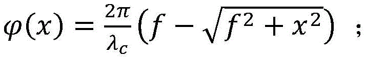
Optionally, the phase of the superlens satisfies:
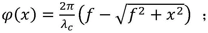
wherein λ is c Is the center wavelength of the light source; f is the focal length of the superlens; and x is a coordinate value of the superlens along the phase change direction.
Optionally, the phase of the superlens satisfies:
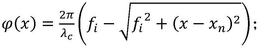
wherein λ c is the central wavelength of the light source; f. of i The focal length of the ith super lens unit in the phase change direction in the super lens; x is a coordinate value of the superlens along the phase change direction; x is a radical of a fluorine atom n Is the center coordinate of the light emitting unit in the nth row or column.
Optionally, the shape of the superlens is an axisymmetric pattern.
Optionally, the superlens is rectangular in shape; the side length of the rectangle satisfies:
L s ≥(N-1)p 1 +2f tanθ+d;
L l ≥(M-1)p 2 +2f tanθ+d;
wherein L is s Is the length of the short side of the rectangle, L l Is the length of the long side of the rectangle; n is the number of the light-emitting units corresponding to the short side; m is the number of the light-emitting units corresponding to the long side; p is a radical of 1 The arrangement period of the light emitting units along the short side direction is set; p is a radical of formula 2 The arrangement period of the light emitting units along the long side direction is set; d is the diameter of the circumscribed circle of the light-emitting unit; theta is a half divergence angle of the light emitting unit; f being said superlensA focal length.
Optionally, the superlens is a transmissive superlens.
Optionally, the superlens is a reflective superlens.
Optionally, the superlens is a chromatic aberration correcting superlens.
Optionally, the divergence angle of the light emitting unit is greater than or equal to 20 ° and less than or equal to 120 °.
Optionally, the fill light further comprises an interval layer;
the spacer layer is used to support the superlens in a wafer level package device of the light source and the superlens.
Optionally, the light source comprises an infrared light emitting unit and/or a visible light emitting unit.
Optionally, the arrangement of the light emitting units satisfies: m is more than 3N.
In a second aspect, an embodiment of the present application further provides a monitoring system, where the monitoring system includes a camera device and at least one fill-in light provided in any of the above embodiments.
The endoscope and the monitoring system comprising the same provided by the embodiment of the application have the following beneficial effects that:
the light filling lamp that this application embodiment provided realizes through setting up in the super lens of light source light-emitting side that the second light beam is greater than or equal to 0 along the divergence angle of super lens phase change direction, and is less than or equal to the divergence angle of first light beam, has realized the miniaturization and the lightweight of light filling lamp.
The monitoring system that this application embodiment provided has realized miniaturization and lightweight through the light filling lamp that at least one this application embodiment provided.
Drawings
In order to more clearly illustrate the technical solutions in the embodiments or the background art of the present application, the drawings required to be used in the embodiments or the background art of the present application will be described below.
Fig. 1 is a schematic view illustrating an alternative structure of a fill-in lamp according to an embodiment of the present disclosure;
fig. 2 is a schematic view illustrating another alternative structure of a fill light provided in an embodiment of the present application;
fig. 3 is a schematic view illustrating another alternative structure of a fill light provided in an embodiment of the present application;
fig. 4 is a schematic view illustrating another alternative structure of a fill light provided in an embodiment of the present application;
fig. 5 is a schematic view illustrating another alternative structure of a fill light provided in an embodiment of the present application;
fig. 6 is a schematic structural diagram illustrating yet another alternative fill light provided in an embodiment of the present application;
fig. 7 is a schematic structural diagram illustrating yet another alternative fill light provided in an embodiment of the present application;
FIG. 8 is a schematic diagram illustrating an alternative arrangement of a superlens provided by an embodiment of the present application;
FIG. 9 is a schematic diagram illustrating an alternative structure of a nanostructure provided by an embodiment of the present application;
FIG. 10 shows a schematic structural diagram of yet another alternative nanostructure provided by an embodiment of the present application;
FIG. 11 is a schematic diagram illustrating an alternative arrangement of nanostructures provided by embodiments of the present application;
FIG. 12 shows a schematic view of yet another alternative arrangement of nanostructures provided by embodiments of the present application;
FIG. 13 is a schematic diagram illustrating yet another alternative arrangement of nanostructures provided by embodiments of the present application;
FIG. 14 is a diagram illustrating an alternative relationship of feature size and phase of nanostructures in a superlens provided by an embodiment of the present application.
In the drawings, the figures respectively show:
10-a superlens; 20-a light source; 30-a spacer layer; 201-a light emitting unit;
101-a base layer; 102-a nanostructure layer; 1021-nanostructures; 1022-filling.
Detailed Description
The present application will now be described more fully hereinafter with reference to the accompanying drawings, in which embodiments are shown. This application may, however, be embodied in many different forms and should not be construed as limited to the embodiments set forth herein. Rather, these embodiments are provided so that this disclosure will be thorough and complete, and will fully convey the scope of the disclosure to those skilled in the art. Like reference numerals refer to like parts throughout. Also, in the drawings, the thickness, ratio and size of the components are exaggerated for clarity of illustration.
The terminology used herein is for the purpose of describing particular embodiments only and is not intended to be limiting. As used herein, "a," "an," "the," and "at least one" do not denote a limitation of quantity, but rather are intended to include both the singular and the plural, unless the context clearly indicates otherwise. For example, "a component" means the same as "at least one component" unless the context clearly dictates otherwise. "at least one of" should not be construed as limited to the quantity "one". "or" means "and/or". The term "and/or" includes any and all combinations of one or more of the associated listed items.
Unless otherwise defined, all terms used herein, including technical and scientific terms, have the same meaning as commonly understood by one of ordinary skill in the art. Terms defined in commonly used dictionaries should be interpreted as having the same meaning as is in the context of the relevant art and will not be interpreted in an idealized or overly formal sense unless expressly so defined herein.
The meaning of "comprising" or "comprises" indicates the property, quantity, step, operation, component, part or combination thereof, but does not exclude other properties, quantities, steps, operations, components, parts or combination thereof.
Embodiments are described herein with reference to cross-sectional views that are idealized embodiments. Thus, variations from the shapes of the illustrations as a result, for example, of manufacturing techniques and/or tolerances, are to be expected. Thus, embodiments described herein should not be construed as limited to the particular shapes of regions as illustrated herein but are to include deviations in shapes that result, for example, from manufacturing. For example, regions shown or described as flat may typically have rough and/or nonlinear features. Also, the acute angles shown may be rounded. Thus, the regions illustrated in the figures are schematic in nature and their shapes are not intended to illustrate the precise shape of a region and are not intended to limit the scope of the claims.
Hereinafter, exemplary embodiments according to the present application will be described with reference to the accompanying drawings.
The embodiment of the present application provides a fill-in light, and as shown in fig. 1 to 7, the fill-in light includes a super lens 10 and a light source 20. The light source 20 includes light emitting units 201 arranged in an array.
Specifically, the phase of the superlens 10 is varied in a direction perpendicular to the optical axis, so that light rays incident at different heights in the direction perpendicular to the optical axis of the superlens are all focused on the same straight line on the focal plane of the superlens. Therefore, the first light beam emitted by the light source 20 is modulated by the superlens 10 to form a second light beam, and the divergence angle of the second light beam along the phase change direction of the superlens 10 is greater than or equal to 0 ° and less than or equal to the divergence angle of the first light beam. In other words, the superlens 10 acts like a collimator for the first light beam emitted by the light source 20. Preferably, the light source 20 is disposed at the focal plane of the superlens 10.
According to the embodiment of the present application, the light source 20 may be an infrared light source or a white light source. Preferably, the light source 20 may also emit infrared light and white light simultaneously or switch between infrared and white light. That is, the light source 20 includes an infrared light emitting unit and/or a white light emitting unit. Optionally, the light source 20 has a center wavelength λ c and a bandwidth Δ λ. Optionally, the divergence angle of any light emitting unit 201 in the light source 20 is greater than or equal to 20 ° and less than or equal to 120 °. According to the embodiment of the present application, the light emitting cells 201 are arranged in an M × N array, where M and N are both natural numbers greater than 1. Preferably, M is greater than 3N.
According to an embodiment of the present application, the superlens 10 is optionally in an axisymmetric pattern, such as a rectangular, circular, or circular ring shape. Exemplarily, FIG. 1 showsThe superlens 10 is shown as rectangular. The short sides of the rectangle correspond to the sides of the N light emitting cells 201 in the light source 20, and the long sides of the rectangle correspond to the sides of the M light emitting cells 201 in the light source 20. In fig. 1 to 3, the z axis is the optical axis direction, the x axis is the short side direction of the rectangle, and the y axis is the long side direction of the rectangle. As shown in FIGS. 2 and 3, the light emitting cells 201 are arranged in the short side direction of the rectangular super lens with a period P 1 The period of the light emitting units 201 arranged along the long side direction of the rectangular superlens is P 2 . It will be appreciated that the dimensions of the individual lighting units 201 are measured in terms of the diameter of their circumscribed circle.
Referring to fig. 1 to 3, an alternative structure of a fill-in lamp is provided in the embodiments of the present application, and a super lens 10 of the fill-in lamp is a single super lens. As shown in fig. 1, the first light beams emitted from all the light emitting units 201 in the light source 20 are modulated by the same superlens. As shown in fig. 2, optionally, the phase of the superlens of the light emitting unit 201 varies in a direction perpendicular to the optical axis, and optionally, the phase of the superlens 10 satisfies formula (1):
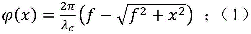
wherein λ is c The center wavelength of the light source 20; f is the focal length of the superlens 10; x is a coordinate value of the superlens 10 in the phase change direction.
Referring to fig. 4 to 6, optionally, the superlens 10 provided in the embodiment of the present application includes a plurality of superlens units arranged in an array. Any one row or column of the superlens 10 corresponds to any one row or column of the light emitting units 201 in the light source 20. As shown in fig. 4 and 6, any superlens unit in the superlens 10 corresponds to any one column of light emitting units 201. Any column of superlens units in the superlens 10 performs quasi-collimated modulation on the first light beams emitted by the light emitting units 201 of the corresponding column. The phase of the superlens satisfies formula (2):
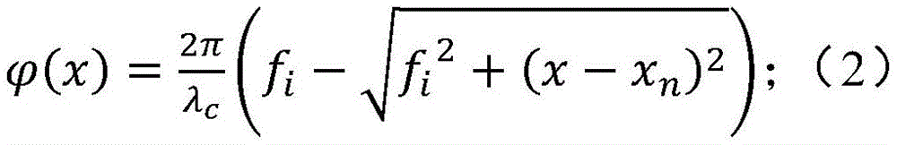
where λ c is the center wavelength of the light source 20; f. of i The focal length of the ith superlens unit in the phase change direction in the superlens 10; x is a coordinate value of the superlens 10 along the phase change direction; x is the number of n Is the center coordinate of the light emitting unit 201 of the nth row or column.
In some alternative embodiments, as shown in fig. 1-7, the superlens 10 is a rectangle having sides with a length that satisfies formula (3) and formula (4):
L s ≥(N-1)p 1 +2f tanθ+d; (3)
L l ≥(M-1)p 2 +2f tanθ+d; (4)
wherein L is s Is the length of the short side of the rectangle, L l The length of the long side of the rectangle; n is the number of light emitting cells 201 corresponding to the short side; m is the number of light emitting cells 201 corresponding to the long side; p is a radical of 1 An arrangement period of the light emitting cells 201 in the short side direction; p is a radical of 2 An arrangement period of the light emitting cells 201 in the long side direction; d is the circumscribed circle diameter of the light emitting unit 201; θ is a half divergence angle of the light emitting unit 201; f is the focal length of the superlens 10.
As shown in fig. 2 or 5, the superlens 10 optionally collimates only one dimension perpendicular to the optical axis, so that the second light beam is irradiated on the region needing supplementary lighting as much as possible. Especially for a security monitoring system, if the irradiation projection area of the second light beam is larger than the focusing area of the camera device, the illumination of the focusing area is insufficient, so that a clear picture cannot be obtained. For example, the projected image of a fill light in a road monitoring system is a rectangle stretched along the road direction, which causes the brightness of the edge of the illuminated surface to be different, resulting in an unclear image in the edge area.
The superlens 10 provided by the embodiment of the present application is compatible with a semiconductor process, and can be wafer-level packaged with the light source 20. The embodiment of the present application further provides a light supplement lamp, referring to fig. 7, in which the superlens 10 and the light source 20 are packaged at a wafer level. As shown in fig. 7, the fill-in light further includes a spacer layer 30, and the spacer layer 30 is used for supporting the superlens 10.
The superlens provided by the embodiment of the present application is described in detail with reference to fig. 8 to 14. As shown in fig. 8, the superlens provided by the embodiment of the present application includes a substrate layer 101 and a nanostructure layer 102. The nanostructure layer 102 includes nanostructures 1021 arranged periodically on one side of the substrate layer 101.
According to an embodiment of the present application, optionally, in the nanostructure layer, the arrangement period of the nanostructures is greater than or equal to 0.3 λ c And is less than or equal to 2 lambda c (ii) a Wherein λ is c The center wavelength of the operating band. According to an embodiment of the present application, optionally, the height of the nanostructures in the nanostructure layer is greater than or equal to 0.3 λ c And is less than or equal to 5 lambda c (ii) a Wherein λ is c The center wavelength of the operating band.
Fig. 9 and 10 show perspective views of nanostructures in a superlens. Optionally, the nanostructure in fig. 9 is a nanofin. Alternatively, the nanostructures in fig. 10 are cylindrical structures. Optionally, as shown in fig. 9 and 10, the superlens further includes a filler 1022, the filler is filled between the nanostructures 1021, and an extinction coefficient of a material of the filler 1022 to a working wavelength band is less than 0.01. Optionally, filler 1022 comprises air or other material that is transparent or translucent in the operating band. According to an embodiment of the present application, the absolute value of the difference between the refractive index of the material of the filler 1022 and the refractive index of the nanostructures 1021 should be greater than or equal to 0.5.
In some alternative embodiments of the present application, as shown in fig. 11 to 13, the nanostructures included in the nanostructure layer 102 are arranged in an array in a form of a close-packed pattern. The vertices and/or central locations of the close-packable pattern are provided with nanostructures 1021. In the embodiments of the present application, the close-packable patterns refer to one or more patterns that can fill the entire plane without gaps and without overlapping.
As shown in fig. 11, the arrangement of nanostructures may be arranged in a fan shape, according to embodiments of the present application. As shown in fig. 12, the arrangement of nanostructures may be arranged in an array of regular hexagons, according to embodiments of the present application. Further, as shown in fig. 13, the arrangement of nanostructures may be arranged in a square array according to embodiments of the present application. Those skilled in the art will recognize that nanostructures may also comprise other forms of array arrangements, and all such variations are within the scope of the present application.
Illustratively, the nanostructures provided by the embodiments of the present application may be polarization-independent structures, which impose a propagation phase on incident light. According to embodiments of the present application, the nanostructures may be positive structures or negative structures. For example, the shape of the nanostructures includes cylinders, hollow cylinders, square prisms, hollow square prisms, and the like.
In alternative embodiments of the present application, the shape of the nanostructures includes cylinders, hollow cylinders, square pillars, and hollow square pillars. Optionally, the nanostructures are disposed in a central position of the close-packable pattern. Optionally, the nanostructure is a negative nanostructure, such as a square pore column, a circular pore column, a square ring column, and a circular ring column.
In an optional implementation manner, the superlens provided in the example of the present application further includes an antireflection film. The antireflection film is arranged on one side of the substrate layer away from the nanostructure layer; alternatively, the antireflection film is disposed on a side of the nanostructure layer adjacent to air. The antireflection film plays a role in antireflection and antireflection for incident light.
According to an embodiment of the present application, the material of the nanostructure is a material having an extinction coefficient of less than 0.01 with respect to the operating band. For example, nanostructured materials include fused silica, quartz glass, crown glass, flint glass, sapphire, crystalline silicon, amorphous silicon, and hydrogenated amorphous silicon. For another example, when the operating wavelength band of the superlens is the near infrared wavelength band, the material of the nanostructure includes one or more of silicon nitride, titanium oxide, gallium nitride, gallium phosphide, hydrogenated amorphous silicon, and crystalline silicon. For another example, when the working wavelength band of the superlens is visible light, the material of the nano-structure includes fused silica, quartz glass, crown glass, flint glass, sapphire and alkali glass. For another example, when the operating wavelength band of the superlens is the far infrared wavelength band, the material of the nanostructure includes one or more of crystalline silicon, crystalline germanium, zinc sulfide and zinc selenide. Figure 14 shows an alternative silicon nitride nanocylinder diameter versus modulation phase.
For example, the material of the substrate layer includes fused quartz, quartz glass, crown glass, flint glass, sapphire, crystalline silicon, amorphous silicon, and hydrogenated amorphous silicon. For another example, when the operating wavelength band of the superlens is the near infrared wavelength band, the material of the substrate layer includes one or more of silicon nitride, titanium oxide, gallium nitride, gallium phosphide, hydrogenated amorphous silicon, and crystalline silicon. As another example, when the working wavelength band of the superlens is the visible wavelength band, the material of the substrate layer includes fused silica, quartz glass, crown glass, flint glass, sapphire, and alkali glass. For another example, when the operating wavelength band of the superlens is the far infrared wavelength band, the material of the substrate layer includes one or more of crystalline silicon, crystalline germanium, zinc sulfide, and zinc selenide.
In some embodiments of the present application, the material of the nanostructures is the same as the material of the base layer. In still other embodiments of the present application, the material of the nanostructures is different from the material of the substrate layer. Optionally, the material of the filler is the same as the material of the base layer. Optionally, the material of the filler is different from the material of the base layer.
It should be understood that in yet other alternative embodiments of the present application, the filler is of a different material than the nanostructures. Illustratively, the material of the filler is a high-transmittance material in the working band, and the extinction coefficient of the high-transmittance material is less than 0.01. Exemplary materials for the filler include fused silica, quartz glass, crown glass, flint glass, sapphire, crystalline silicon, amorphous silicon, and hydrogenated amorphous silicon.
According to an embodiment of the present application, the phase of the superlens satisfies at least one of the following equations (1-1) to (1-6):


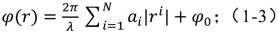


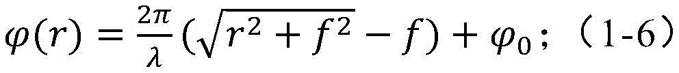
wherein r is the distance from the center of the superlens to the center of any nanostructure; lambda is the wavelength of operation and, x, y are the mirror coordinates of the superlens, and f is the focal length of the first superlens.
The phase of the superlens may be expressed in higher order polynomials, including odd and even polynomials. In order not to destroy the rotational symmetry of the phase of the superlens, the phase corresponding to the even-order polynomial can be optimized, which greatly reduces the degree of freedom of the design of the superlens. In the formulas (1-1) to (1-6), compared with the other formulas (1-3) and (1-4), the phase satisfying the odd polynomial can be optimized without destroying the rotational symmetry of the phase of the superlens, so that the optimization degree of freedom of the superlens is greatly improved.
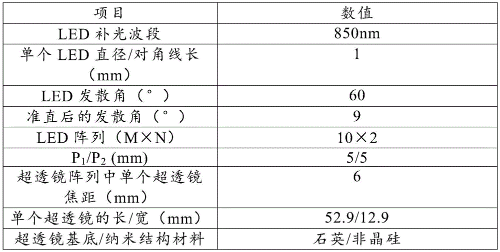
Example 1
Embodiment 1 provides a fill-in lamp, and system parameters of the fill-in lamp are shown in table 1.
TABLE 1
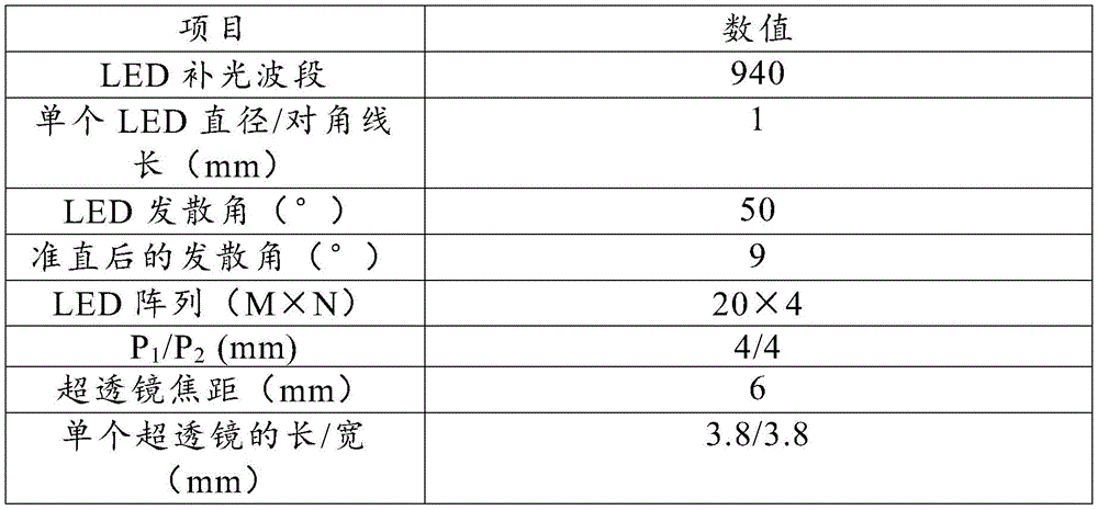
Example 2
TABLE 2

On the other hand, an embodiment of the present application further provides a monitoring system, where the monitoring system includes a camera device and at least one light supplement lamp provided in any one of the above embodiments.
In some optional embodiments, the monitoring system provided by the embodiments of the present application includes at least two superlenses 10. Wherein the directions of phase change of at least two superlenses 10 are orthogonal, convergent collimation can be performed in both orthogonal directions (e.g. x-direction and y-direction) perpendicular to the optical axis. The convergence collimation in one direction is to improve the illumination of the edge area projected by the light supplement lamp; the convergence collimation in the other direction is to reduce the divergence angle of the emergent light beam (second light beam) of the light supplement lamp in the other direction, reduce the overlapping area of the irradiation projection, and improve the irradiation uniformity of the light supplement lamp, so that the risk of dazzling and even instant blinding due to overhigh light intensity of the partial projection area of the light supplement lamp is avoided.
To sum up, the light filling lamp that this application embodiment provided realizes through the super lens that sets up in light source light-emitting side that the divergence angle of second light beam along super lens phase change direction is greater than or equal to 0, and is less than or equal to the divergence angle of first light beam, has realized the miniaturization and the lightweight of light filling lamp.
The monitoring system that this application embodiment provided has realized miniaturization and lightweight through the light filling lamp that at least one this application embodiment provided. The above description is only a specific implementation of the embodiments of the present application, but the scope of the embodiments of the present application is not limited thereto, and any person skilled in the art can easily think of the changes or substitutions within the technical scope of the embodiments of the present application, and all the changes or substitutions should be covered within the scope of the embodiments of the present application. Therefore, the protection scope of the embodiments of the present application shall be subject to the protection scope of the claims.
Claims (16)
1. A light supplement lamp is characterized by comprising a super lens (10) and a light source (20);
wherein the superlens (10) is arranged at the light exit side of the light source (20);
the light source (20) comprises a plurality of light emitting units (201) arranged in an array;
the superlens (10) is arranged on the light-emitting side of the light source (20); the phase of the super lens (10) changes along the direction vertical to the optical axis, so that light rays incident at different heights in the direction vertical to the optical axis of the super lens (10) are all focused on the same straight line on the focal plane of the super lens (10), a first light beam emitted by the light source (20) is modulated by the super lens (10) to form a second light beam, and the divergence angle of the second light beam along the phase change direction of the super lens (10) is larger than or equal to 0 DEG and smaller than or equal to that of the first light beam.
2. A fill-in light as claimed in claim 1, wherein the light emitting units (201) are arranged in an mxn array;
m and N are both natural numbers larger than or equal to 1.
3. A fill-in light as claimed in claim 1, wherein the superlens (10) is a monolithic superlens.
4. A fill-in light as claimed in claim 1, wherein the superlens (10) is an array superlens; the array type super lens comprises a plurality of super lens units arranged in an array mode.
5. A fill-in light as claimed in claim 3, wherein the phase of the superlens (10) is such that:
wherein λ is c Is the center wavelength of the light source (20); f is the focal length of the superlens (10); x is a coordinate value of the superlens (10) along the phase change direction.
6. A fill-in lamp as claimed in claim 4, wherein the phase of the superlens (10) is such that:

wherein λ c is the central wavelength of the light source (20); f. of i The focal length of the ith super lens unit in the phase change direction in the super lens (10); x is a coordinate value of the superlens (10) along the phase change direction; x is the number of n Is the center coordinate of the light-emitting unit (201) in the nth row or nth column.
7. A fill-in light as claimed in any one of claims 1 or 3-6, wherein the superlens (10) is shaped as an axisymmetric figure.
8. A fill-in light as claimed in claim 7, wherein the superlens (10) is rectangular in shape; the side length of the rectangle satisfies:
L s ≥(N-1)p 1 +2f tan θ+d;
L l ≥(M-1)p 2 +2f tanθ +d;
wherein L is s Is the length of the short side of the rectangle, L l Is the length of the long side of the rectangle; n is the number of light-emitting units (201) corresponding to the short side; m is the number of the light-emitting units (201) corresponding to the long side; p is a radical of 1 Is the arrangement period of the light emitting units (201) along the short side direction; p is a radical of formula 2 Is a light emitting unit (201)An arrangement period in the longitudinal direction; d is the diameter of the circumscribed circle of the light-emitting unit (201); theta is a half divergence angle of the light emitting unit (201); f is the focal length of the superlens (10).
9. A fill light as claimed in any of claims 1 or 3 to 6, wherein the superlens (10) is a transmissive superlens.
10. A fill-in light as claimed in any one of claims 1 or 3-6, wherein the super lens (10) is a reflective super lens.
11. A fill light as claimed in any of claims 1 or 3 to 6, wherein the superlens (10) is a chromatic aberration correcting superlens.
12. A fill-in light as claimed in claim 1, wherein the divergence angle of the light emitting unit (201) is greater than or equal to 20 ° and less than or equal to 120 °.
13. A fill-in light as claimed in claim 1, further comprising a spacer layer (30);
the spacer layer (30) is used to support the superlens (10) in a wafer-level package device of the light source (20) and the superlens (10).
14. A fill-in light as claimed in claim 1, wherein the light source (20) comprises an infrared light emitting unit and/or a visible light emitting unit.
15. A fill-in light as defined in claim 2, wherein the arrangement of the light emitting units (201) is such that: m is more than 3N.
16. A monitoring system, characterized in that the monitoring system comprises a camera device and at least one fill-in light according to claims 1-12.
Priority Applications (1)
| Application Number | Priority Date | Filing Date | Title |
|---|---|---|---|
| CN202222176477.8U CN217982089U (en) | 2022-08-17 | 2022-08-17 | Light filling lamp and monitoring system comprising same |
Applications Claiming Priority (1)
| Application Number | Priority Date | Filing Date | Title |
|---|---|---|---|
| CN202222176477.8U CN217982089U (en) | 2022-08-17 | 2022-08-17 | Light filling lamp and monitoring system comprising same |
Publications (1)
| Publication Number | Publication Date |
|---|---|
| CN217982089U true CN217982089U (en) | 2022-12-06 |
Family
ID=84259714
Family Applications (1)
| Application Number | Title | Priority Date | Filing Date |
|---|---|---|---|
| CN202222176477.8U Active CN217982089U (en) | 2022-08-17 | 2022-08-17 | Light filling lamp and monitoring system comprising same |
Country Status (1)
| Country | Link |
|---|---|
| CN (1) | CN217982089U (en) |
Cited By (9)
| Publication number | Priority date | Publication date | Assignee | Title |
|---|---|---|---|---|
| CN115933210A (en) * | 2022-12-26 | 2023-04-07 | 苏州山河光电科技有限公司 | Optical device and package structure of optical device |
| CN116009270A (en) * | 2023-01-06 | 2023-04-25 | 深圳迈塔兰斯科技有限公司 | A collimating optical element and its design method |
| US11927769B2 (en) | 2022-03-31 | 2024-03-12 | Metalenz, Inc. | Polarization sorting metasurface microlens array device |
| US11978752B2 (en) | 2019-07-26 | 2024-05-07 | Metalenz, Inc. | Aperture-metasurface and hybrid refractive-metasurface imaging systems |
| US11988844B2 (en) | 2017-08-31 | 2024-05-21 | Metalenz, Inc. | Transmissive metasurface lens integration |
| US12140778B2 (en) | 2018-07-02 | 2024-11-12 | Metalenz, Inc. | Metasurfaces for laser speckle reduction |
| US12416752B2 (en) | 2018-01-24 | 2025-09-16 | President And Fellows Of Harvard College | Polarization state generation with a metasurface |
| US12460919B2 (en) | 2019-10-31 | 2025-11-04 | President And Fellows Of Harvard College | Compact metalens depth sensors |
| US12548980B2 (en) | 2022-05-25 | 2026-02-10 | Metalenz, Inc. | Single element dot pattern projector |
-
2022
- 2022-08-17 CN CN202222176477.8U patent/CN217982089U/en active Active
Cited By (12)
| Publication number | Priority date | Publication date | Assignee | Title |
|---|---|---|---|---|
| US11988844B2 (en) | 2017-08-31 | 2024-05-21 | Metalenz, Inc. | Transmissive metasurface lens integration |
| US12411348B2 (en) | 2017-08-31 | 2025-09-09 | Metalenz, Inc. | Transmissive metasurface lens integration |
| US12416752B2 (en) | 2018-01-24 | 2025-09-16 | President And Fellows Of Harvard College | Polarization state generation with a metasurface |
| US12140778B2 (en) | 2018-07-02 | 2024-11-12 | Metalenz, Inc. | Metasurfaces for laser speckle reduction |
| US11978752B2 (en) | 2019-07-26 | 2024-05-07 | Metalenz, Inc. | Aperture-metasurface and hybrid refractive-metasurface imaging systems |
| US12389700B2 (en) | 2019-07-26 | 2025-08-12 | Metalenz, Inc. | Aperture-metasurface and hybrid refractive-metasurface imaging systems |
| US12460919B2 (en) | 2019-10-31 | 2025-11-04 | President And Fellows Of Harvard College | Compact metalens depth sensors |
| US11927769B2 (en) | 2022-03-31 | 2024-03-12 | Metalenz, Inc. | Polarization sorting metasurface microlens array device |
| US12276807B2 (en) | 2022-03-31 | 2025-04-15 | Metalenz, Inc. | Polarization sorting metasurface microlens array device |
| US12548980B2 (en) | 2022-05-25 | 2026-02-10 | Metalenz, Inc. | Single element dot pattern projector |
| CN115933210A (en) * | 2022-12-26 | 2023-04-07 | 苏州山河光电科技有限公司 | Optical device and package structure of optical device |
| CN116009270A (en) * | 2023-01-06 | 2023-04-25 | 深圳迈塔兰斯科技有限公司 | A collimating optical element and its design method |
Similar Documents
| Publication | Publication Date | Title |
|---|---|---|
| CN217982089U (en) | Light filling lamp and monitoring system comprising same | |
| CN217820839U (en) | 3D-ToF emission module and depth camera comprising same | |
| CN216896898U (en) | Automobile projection lamp based on super lens | |
| CN217279244U (en) | Projection system | |
| US10317579B2 (en) | Optical device with a collimator and lenslet arrays | |
| CN217981833U (en) | ToF emission module and electronic equipment comprising same | |
| CN217820943U (en) | ToF emission module and electronic equipment comprising same | |
| CN110161602B (en) | Diffusion plate, method for designing diffusion plate, display device, projection device, and illumination device | |
| EP1714499A2 (en) | Illumination system | |
| EP1733255A1 (en) | Light-collecting illumination system | |
| WO2005078496A2 (en) | Reshaping light source modules and illumination systems using the same | |
| EP3822693A2 (en) | Head-mounted display | |
| US12360293B2 (en) | Micro-lens array, projection type image display device, method for designing micro-lens array, and method for manufacturing micro-lens array | |
| WO2022217976A1 (en) | Optical element and optical module | |
| CN212256002U (en) | Head-up display device and motor vehicle | |
| CN114879290A (en) | Diffusion sheet and head-up display device | |
| EP1631855B1 (en) | Compact led module and projection display adopting the same | |
| US11892154B2 (en) | Illumination device | |
| US20100289035A1 (en) | Optoelectronic device and image recording device | |
| WO2022034926A1 (en) | Optical system, display device, projection device, and illumination device | |
| CN217543434U (en) | Diffusion sheet and head-up display device | |
| CN118444492A (en) | Collimation optical element | |
| US8089614B2 (en) | Device for changing pitch between light beam axes, and substrate exposure apparatus | |
| JP7655337B2 (en) | Light source device and projector | |
| CN116105096B (en) | Light-mixing and converging optics for dental lighting |
Legal Events
| Date | Code | Title | Description |
|---|---|---|---|
| GR01 | Patent grant | ||
| GR01 | Patent grant |